JP4608105B2 - Organic electroluminescence display device and manufacturing method thereof - Google Patents
Organic electroluminescence display device and manufacturing method thereof Download PDFInfo
- Publication number
- JP4608105B2 JP4608105B2 JP2000610259A JP2000610259A JP4608105B2 JP 4608105 B2 JP4608105 B2 JP 4608105B2 JP 2000610259 A JP2000610259 A JP 2000610259A JP 2000610259 A JP2000610259 A JP 2000610259A JP 4608105 B2 JP4608105 B2 JP 4608105B2
- Authority
- JP
- Japan
- Prior art keywords
- lower electrode
- wiring layer
- auxiliary wiring
- organic
- display device
- Prior art date
- Legal status (The legal status is an assumption and is not a legal conclusion. Google has not performed a legal analysis and makes no representation as to the accuracy of the status listed.)
- Expired - Lifetime
Links
- 238000005401 electroluminescence Methods 0.000 title claims description 13
- 238000004519 manufacturing process Methods 0.000 title description 51
- 239000000758 substrate Substances 0.000 claims description 44
- 239000010410 layer Substances 0.000 description 367
- 229910052751 metal Inorganic materials 0.000 description 32
- 239000002184 metal Substances 0.000 description 32
- 230000007547 defect Effects 0.000 description 30
- 239000000463 material Substances 0.000 description 27
- 230000002829 reductive effect Effects 0.000 description 23
- 238000000034 method Methods 0.000 description 22
- 239000011651 chromium Substances 0.000 description 17
- 229910052804 chromium Inorganic materials 0.000 description 14
- WGTYBPLFGIVFAS-UHFFFAOYSA-M tetramethylammonium hydroxide Chemical compound [OH-].C[N+](C)(C)C WGTYBPLFGIVFAS-UHFFFAOYSA-M 0.000 description 14
- VYZAMTAEIAYCRO-UHFFFAOYSA-N Chromium Chemical compound [Cr] VYZAMTAEIAYCRO-UHFFFAOYSA-N 0.000 description 13
- 239000000470 constituent Substances 0.000 description 12
- 230000015572 biosynthetic process Effects 0.000 description 11
- 239000011159 matrix material Substances 0.000 description 11
- 239000004020 conductor Substances 0.000 description 10
- 238000010292 electrical insulation Methods 0.000 description 10
- 229920002120 photoresistant polymer Polymers 0.000 description 10
- 229910052782 aluminium Inorganic materials 0.000 description 9
- XAGFODPZIPBFFR-UHFFFAOYSA-N aluminium Chemical compound [Al] XAGFODPZIPBFFR-UHFFFAOYSA-N 0.000 description 9
- 238000000151 deposition Methods 0.000 description 8
- 229910045601 alloy Inorganic materials 0.000 description 7
- 239000000956 alloy Substances 0.000 description 7
- 230000008021 deposition Effects 0.000 description 7
- 238000011156 evaluation Methods 0.000 description 7
- 239000011521 glass Substances 0.000 description 7
- QTBSBXVTEAMEQO-UHFFFAOYSA-N Acetic acid Chemical compound CC(O)=O QTBSBXVTEAMEQO-UHFFFAOYSA-N 0.000 description 6
- 230000000052 comparative effect Effects 0.000 description 6
- -1 for example Inorganic materials 0.000 description 6
- 239000000243 solution Substances 0.000 description 6
- 229910004298 SiO 2 Inorganic materials 0.000 description 5
- 239000010949 copper Substances 0.000 description 5
- 239000010931 gold Substances 0.000 description 5
- 229910052709 silver Inorganic materials 0.000 description 5
- 238000004544 sputter deposition Methods 0.000 description 5
- 238000007740 vapor deposition Methods 0.000 description 5
- KDLHZDBZIXYQEI-UHFFFAOYSA-N Palladium Chemical compound [Pd] KDLHZDBZIXYQEI-UHFFFAOYSA-N 0.000 description 4
- NBIIXXVUZAFLBC-UHFFFAOYSA-N Phosphoric acid Chemical compound OP(O)(O)=O NBIIXXVUZAFLBC-UHFFFAOYSA-N 0.000 description 4
- 235000010724 Wisteria floribunda Nutrition 0.000 description 4
- XLOMVQKBTHCTTD-UHFFFAOYSA-N Zinc monoxide Chemical compound [Zn]=O XLOMVQKBTHCTTD-UHFFFAOYSA-N 0.000 description 4
- 239000007864 aqueous solution Substances 0.000 description 4
- 238000009826 distribution Methods 0.000 description 4
- 230000000694 effects Effects 0.000 description 4
- 238000002347 injection Methods 0.000 description 4
- 239000007924 injection Substances 0.000 description 4
- 239000000203 mixture Substances 0.000 description 4
- 229910052750 molybdenum Inorganic materials 0.000 description 4
- VLTRZXGMWDSKGL-UHFFFAOYSA-N perchloric acid Chemical compound OCl(=O)(=O)=O VLTRZXGMWDSKGL-UHFFFAOYSA-N 0.000 description 4
- 239000004065 semiconductor Substances 0.000 description 4
- 229910052721 tungsten Inorganic materials 0.000 description 4
- UHXOHPVVEHBKKT-UHFFFAOYSA-N 1-(2,2-diphenylethenyl)-4-[4-(2,2-diphenylethenyl)phenyl]benzene Chemical group C=1C=C(C=2C=CC(C=C(C=3C=CC=CC=3)C=3C=CC=CC=3)=CC=2)C=CC=1C=C(C=1C=CC=CC=1)C1=CC=CC=C1 UHXOHPVVEHBKKT-UHFFFAOYSA-N 0.000 description 3
- KFZMGEQAYNKOFK-UHFFFAOYSA-N Isopropanol Chemical compound CC(C)O KFZMGEQAYNKOFK-UHFFFAOYSA-N 0.000 description 3
- ZOKXTWBITQBERF-UHFFFAOYSA-N Molybdenum Chemical compound [Mo] ZOKXTWBITQBERF-UHFFFAOYSA-N 0.000 description 3
- PXHVJJICTQNCMI-UHFFFAOYSA-N Nickel Chemical compound [Ni] PXHVJJICTQNCMI-UHFFFAOYSA-N 0.000 description 3
- MUBZPKHOEPUJKR-UHFFFAOYSA-N Oxalic acid Chemical compound OC(=O)C(O)=O MUBZPKHOEPUJKR-UHFFFAOYSA-N 0.000 description 3
- BQCADISMDOOEFD-UHFFFAOYSA-N Silver Chemical compound [Ag] BQCADISMDOOEFD-UHFFFAOYSA-N 0.000 description 3
- NIXOWILDQLNWCW-UHFFFAOYSA-N acrylic acid group Chemical group C(C=C)(=O)O NIXOWILDQLNWCW-UHFFFAOYSA-N 0.000 description 3
- 230000002411 adverse Effects 0.000 description 3
- 229910052802 copper Inorganic materials 0.000 description 3
- 238000005530 etching Methods 0.000 description 3
- 239000011777 magnesium Substances 0.000 description 3
- 150000002739 metals Chemical class 0.000 description 3
- 239000011733 molybdenum Substances 0.000 description 3
- 238000000206 photolithography Methods 0.000 description 3
- BASFCYQUMIYNBI-UHFFFAOYSA-N platinum Chemical compound [Pt] BASFCYQUMIYNBI-UHFFFAOYSA-N 0.000 description 3
- 229920000642 polymer Polymers 0.000 description 3
- 230000008569 process Effects 0.000 description 3
- 229910052715 tantalum Inorganic materials 0.000 description 3
- CPELXLSAUQHCOX-UHFFFAOYSA-N Hydrogen bromide Chemical compound Br CPELXLSAUQHCOX-UHFFFAOYSA-N 0.000 description 2
- FYYHWMGAXLPEAU-UHFFFAOYSA-N Magnesium Chemical compound [Mg] FYYHWMGAXLPEAU-UHFFFAOYSA-N 0.000 description 2
- 229910052779 Neodymium Inorganic materials 0.000 description 2
- GRYLNZFGIOXLOG-UHFFFAOYSA-N Nitric acid Chemical compound O[N+]([O-])=O GRYLNZFGIOXLOG-UHFFFAOYSA-N 0.000 description 2
- CTQNGGLPUBDAKN-UHFFFAOYSA-N O-Xylene Chemical compound CC1=CC=CC=C1C CTQNGGLPUBDAKN-UHFFFAOYSA-N 0.000 description 2
- 239000004642 Polyimide Substances 0.000 description 2
- 229910006404 SnO 2 Inorganic materials 0.000 description 2
- 229910000831 Steel Inorganic materials 0.000 description 2
- 229910000147 aluminium phosphate Inorganic materials 0.000 description 2
- QVGXLLKOCUKJST-UHFFFAOYSA-N atomic oxygen Chemical compound [O] QVGXLLKOCUKJST-UHFFFAOYSA-N 0.000 description 2
- 229910052799 carbon Inorganic materials 0.000 description 2
- XMPZTFVPEKAKFH-UHFFFAOYSA-P ceric ammonium nitrate Chemical compound [NH4+].[NH4+].[Ce+4].[O-][N+]([O-])=O.[O-][N+]([O-])=O.[O-][N+]([O-])=O.[O-][N+]([O-])=O.[O-][N+]([O-])=O.[O-][N+]([O-])=O XMPZTFVPEKAKFH-UHFFFAOYSA-P 0.000 description 2
- 125000005678 ethenylene group Chemical group [H]C([*:1])=C([H])[*:2] 0.000 description 2
- PCHJSUWPFVWCPO-UHFFFAOYSA-N gold Chemical compound [Au] PCHJSUWPFVWCPO-UHFFFAOYSA-N 0.000 description 2
- 229910052737 gold Inorganic materials 0.000 description 2
- 238000010438 heat treatment Methods 0.000 description 2
- 238000009413 insulation Methods 0.000 description 2
- 238000010030 laminating Methods 0.000 description 2
- 229910052749 magnesium Inorganic materials 0.000 description 2
- 229910017604 nitric acid Inorganic materials 0.000 description 2
- 150000004767 nitrides Chemical class 0.000 description 2
- 239000001301 oxygen Substances 0.000 description 2
- 229910052760 oxygen Inorganic materials 0.000 description 2
- 238000000059 patterning Methods 0.000 description 2
- 230000035699 permeability Effects 0.000 description 2
- 229920001721 polyimide Polymers 0.000 description 2
- 229910052761 rare earth metal Inorganic materials 0.000 description 2
- 150000002910 rare earth metals Chemical class 0.000 description 2
- 229910052710 silicon Inorganic materials 0.000 description 2
- 239000010703 silicon Substances 0.000 description 2
- 239000004332 silver Substances 0.000 description 2
- 239000002356 single layer Substances 0.000 description 2
- 239000010959 steel Substances 0.000 description 2
- 230000003746 surface roughness Effects 0.000 description 2
- 239000010936 titanium Substances 0.000 description 2
- 238000002834 transmittance Methods 0.000 description 2
- WFKWXMTUELFFGS-UHFFFAOYSA-N tungsten Chemical compound [W] WFKWXMTUELFFGS-UHFFFAOYSA-N 0.000 description 2
- 239000010937 tungsten Substances 0.000 description 2
- XLYOFNOQVPJJNP-UHFFFAOYSA-N water Substances O XLYOFNOQVPJJNP-UHFFFAOYSA-N 0.000 description 2
- 239000008096 xylene Substances 0.000 description 2
- 239000011787 zinc oxide Substances 0.000 description 2
- HONWGFNQCPRRFM-UHFFFAOYSA-N 2-n-(3-methylphenyl)-1-n,1-n,2-n-triphenylbenzene-1,2-diamine Chemical compound CC1=CC=CC(N(C=2C=CC=CC=2)C=2C(=CC=CC=2)N(C=2C=CC=CC=2)C=2C=CC=CC=2)=C1 HONWGFNQCPRRFM-UHFFFAOYSA-N 0.000 description 1
- VLJQDHDVZJXNQL-UHFFFAOYSA-N 4-methyl-n-(oxomethylidene)benzenesulfonamide Chemical compound CC1=CC=C(S(=O)(=O)N=C=O)C=C1 VLJQDHDVZJXNQL-UHFFFAOYSA-N 0.000 description 1
- 229910018072 Al 2 O 3 Inorganic materials 0.000 description 1
- 229910001148 Al-Li alloy Inorganic materials 0.000 description 1
- 229910018134 Al-Mg Inorganic materials 0.000 description 1
- 229910018467 Al—Mg Inorganic materials 0.000 description 1
- 229910018575 Al—Ti Inorganic materials 0.000 description 1
- 229910018580 Al—Zr Inorganic materials 0.000 description 1
- OKTJSMMVPCPJKN-UHFFFAOYSA-N Carbon Chemical compound [C] OKTJSMMVPCPJKN-UHFFFAOYSA-N 0.000 description 1
- 229910019001 CoSi Inorganic materials 0.000 description 1
- RYGMFSIKBFXOCR-UHFFFAOYSA-N Copper Chemical compound [Cu] RYGMFSIKBFXOCR-UHFFFAOYSA-N 0.000 description 1
- 229910019974 CrSi Inorganic materials 0.000 description 1
- 229910005881 NiSi 2 Inorganic materials 0.000 description 1
- 229920000292 Polyquinoline Polymers 0.000 description 1
- 229910020923 Sn-O Inorganic materials 0.000 description 1
- PJANXHGTPQOBST-VAWYXSNFSA-N Stilbene Natural products C=1C=CC=CC=1/C=C/C1=CC=CC=C1 PJANXHGTPQOBST-VAWYXSNFSA-N 0.000 description 1
- 229910008484 TiSi Inorganic materials 0.000 description 1
- ATJFFYVFTNAWJD-UHFFFAOYSA-N Tin Chemical compound [Sn] ATJFFYVFTNAWJD-UHFFFAOYSA-N 0.000 description 1
- RTAQQCXQSZGOHL-UHFFFAOYSA-N Titanium Chemical compound [Ti] RTAQQCXQSZGOHL-UHFFFAOYSA-N 0.000 description 1
- 239000007983 Tris buffer Substances 0.000 description 1
- 229910007541 Zn O Inorganic materials 0.000 description 1
- 229910006249 ZrSi Inorganic materials 0.000 description 1
- 229910052783 alkali metal Inorganic materials 0.000 description 1
- 150000001340 alkali metals Chemical class 0.000 description 1
- 229910052784 alkaline earth metal Inorganic materials 0.000 description 1
- 229910000287 alkaline earth metal oxide Inorganic materials 0.000 description 1
- 150000001342 alkaline earth metals Chemical class 0.000 description 1
- 229910021431 alpha silicon carbide Inorganic materials 0.000 description 1
- HSFWRNGVRCDJHI-UHFFFAOYSA-N alpha-acetylene Natural products C#C HSFWRNGVRCDJHI-UHFFFAOYSA-N 0.000 description 1
- 229910052788 barium Inorganic materials 0.000 description 1
- 229910052791 calcium Inorganic materials 0.000 description 1
- 239000000919 ceramic Substances 0.000 description 1
- 238000006243 chemical reaction Methods 0.000 description 1
- 239000011248 coating agent Substances 0.000 description 1
- 238000000576 coating method Methods 0.000 description 1
- 150000001875 compounds Chemical class 0.000 description 1
- 229920000547 conjugated polymer Polymers 0.000 description 1
- 230000007797 corrosion Effects 0.000 description 1
- 238000005260 corrosion Methods 0.000 description 1
- 125000004122 cyclic group Chemical group 0.000 description 1
- 230000003247 decreasing effect Effects 0.000 description 1
- KPUWHANPEXNPJT-UHFFFAOYSA-N disiloxane Chemical class [SiH3]O[SiH3] KPUWHANPEXNPJT-UHFFFAOYSA-N 0.000 description 1
- 238000006073 displacement reaction Methods 0.000 description 1
- 230000005611 electricity Effects 0.000 description 1
- 239000007772 electrode material Substances 0.000 description 1
- 239000007789 gas Substances 0.000 description 1
- 230000005525 hole transport Effects 0.000 description 1
- 229910000042 hydrogen bromide Inorganic materials 0.000 description 1
- AMGQUBHHOARCQH-UHFFFAOYSA-N indium;oxotin Chemical compound [In].[Sn]=O AMGQUBHHOARCQH-UHFFFAOYSA-N 0.000 description 1
- 229910052809 inorganic oxide Inorganic materials 0.000 description 1
- 239000011810 insulating material Substances 0.000 description 1
- 230000002452 interceptive effect Effects 0.000 description 1
- 230000000670 limiting effect Effects 0.000 description 1
- 239000007788 liquid Substances 0.000 description 1
- IBHBKWKFFTZAHE-UHFFFAOYSA-N n-[4-[4-(n-naphthalen-1-ylanilino)phenyl]phenyl]-n-phenylnaphthalen-1-amine Chemical group C1=CC=CC=C1N(C=1C2=CC=CC=C2C=CC=1)C1=CC=C(C=2C=CC(=CC=2)N(C=2C=CC=CC=2)C=2C3=CC=CC=C3C=CC=2)C=C1 IBHBKWKFFTZAHE-UHFFFAOYSA-N 0.000 description 1
- QEFYFXOXNSNQGX-UHFFFAOYSA-N neodymium atom Chemical compound [Nd] QEFYFXOXNSNQGX-UHFFFAOYSA-N 0.000 description 1
- 229910052759 nickel Inorganic materials 0.000 description 1
- 239000012044 organic layer Substances 0.000 description 1
- 235000006408 oxalic acid Nutrition 0.000 description 1
- 229910052763 palladium Inorganic materials 0.000 description 1
- 230000036961 partial effect Effects 0.000 description 1
- 229910052697 platinum Inorganic materials 0.000 description 1
- 229910021340 platinum monosilicide Inorganic materials 0.000 description 1
- 229920000553 poly(phenylenevinylene) Polymers 0.000 description 1
- 229920002492 poly(sulfone) Polymers 0.000 description 1
- 229920001197 polyacetylene Polymers 0.000 description 1
- 229920000058 polyacrylate Polymers 0.000 description 1
- 229920000767 polyaniline Polymers 0.000 description 1
- 229920001230 polyarylate Polymers 0.000 description 1
- 229920000412 polyarylene Polymers 0.000 description 1
- 229920000515 polycarbonate Polymers 0.000 description 1
- 239000004417 polycarbonate Substances 0.000 description 1
- 229910021420 polycrystalline silicon Inorganic materials 0.000 description 1
- 229920000098 polyolefin Polymers 0.000 description 1
- 229920000128 polypyrrole Polymers 0.000 description 1
- 230000009467 reduction Effects 0.000 description 1
- 230000004044 response Effects 0.000 description 1
- 229910052706 scandium Inorganic materials 0.000 description 1
- 229910021332 silicide Inorganic materials 0.000 description 1
- FVBUAEGBCNSCDD-UHFFFAOYSA-N silicide(4-) Chemical compound [Si-4] FVBUAEGBCNSCDD-UHFFFAOYSA-N 0.000 description 1
- 150000003377 silicon compounds Chemical class 0.000 description 1
- 238000004528 spin coating Methods 0.000 description 1
- PJANXHGTPQOBST-UHFFFAOYSA-N stilbene Chemical compound C=1C=CC=CC=1C=CC1=CC=CC=C1 PJANXHGTPQOBST-UHFFFAOYSA-N 0.000 description 1
- 235000021286 stilbenes Nutrition 0.000 description 1
- GUVRBAGPIYLISA-UHFFFAOYSA-N tantalum atom Chemical compound [Ta] GUVRBAGPIYLISA-UHFFFAOYSA-N 0.000 description 1
- ANRHNWWPFJCPAZ-UHFFFAOYSA-M thionine Chemical compound [Cl-].C1=CC(N)=CC2=[S+]C3=CC(N)=CC=C3N=C21 ANRHNWWPFJCPAZ-UHFFFAOYSA-M 0.000 description 1
- 229910052719 titanium Inorganic materials 0.000 description 1
- YVTHLONGBIQYBO-UHFFFAOYSA-N zinc indium(3+) oxygen(2-) Chemical compound [O--].[Zn++].[In+3] YVTHLONGBIQYBO-UHFFFAOYSA-N 0.000 description 1
Images


Classifications
-
- H—ELECTRICITY
- H10—SEMICONDUCTOR DEVICES; ELECTRIC SOLID-STATE DEVICES NOT OTHERWISE PROVIDED FOR
- H10K—ORGANIC ELECTRIC SOLID-STATE DEVICES
- H10K59/00—Integrated devices, or assemblies of multiple devices, comprising at least one organic light-emitting element covered by group H10K50/00
- H10K59/10—OLED displays
- H10K59/17—Passive-matrix OLED displays
-
- H—ELECTRICITY
- H05—ELECTRIC TECHNIQUES NOT OTHERWISE PROVIDED FOR
- H05B—ELECTRIC HEATING; ELECTRIC LIGHT SOURCES NOT OTHERWISE PROVIDED FOR; CIRCUIT ARRANGEMENTS FOR ELECTRIC LIGHT SOURCES, IN GENERAL
- H05B33/00—Electroluminescent light sources
- H05B33/12—Light sources with substantially two-dimensional radiating surfaces
- H05B33/26—Light sources with substantially two-dimensional radiating surfaces characterised by the composition or arrangement of the conductive material used as an electrode
-
- H—ELECTRICITY
- H10—SEMICONDUCTOR DEVICES; ELECTRIC SOLID-STATE DEVICES NOT OTHERWISE PROVIDED FOR
- H10K—ORGANIC ELECTRIC SOLID-STATE DEVICES
- H10K50/00—Organic light-emitting devices
- H10K50/80—Constructional details
- H10K50/805—Electrodes
- H10K50/81—Anodes
- H10K50/814—Anodes combined with auxiliary electrodes, e.g. ITO layer combined with metal lines
-
- H—ELECTRICITY
- H10—SEMICONDUCTOR DEVICES; ELECTRIC SOLID-STATE DEVICES NOT OTHERWISE PROVIDED FOR
- H10K—ORGANIC ELECTRIC SOLID-STATE DEVICES
- H10K59/00—Integrated devices, or assemblies of multiple devices, comprising at least one organic light-emitting element covered by group H10K50/00
- H10K59/80—Constructional details
- H10K59/805—Electrodes
- H10K59/8051—Anodes
- H10K59/80516—Anodes combined with auxiliary electrodes, e.g. ITO layer combined with metal lines
Landscapes
- Physics & Mathematics (AREA)
- Optics & Photonics (AREA)
- Electroluminescent Light Sources (AREA)
- Devices For Indicating Variable Information By Combining Individual Elements (AREA)
Description
技術分野
この発明は、有機エレクトロルミネッセンス表示装置(以下、有機EL表示装置と称する場合がある。)およびその製造方法に関する。
さらに詳しくは、民生用および工業用の表示機器(ディスプレイ)に好適なように、発光画素面積が大きい有機EL表示装置およびそのような有機EL表示装置が効率的に得られる製造方法に関する。
背景技術
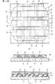
従来、電極間に発光層を挟持して構成したEL素子を、マトリクス状に配した走査電極線や信号電極線を介して駆動(発光)させるEL表示装置が提案されているが、発光画素の高精細化のために、走査電極線等の配線抵抗による電圧降下や、応答遅延を防止することが要求されている。
このため、第17図に示すように、ガラス基板101上に、第1透明電極(下部電極)102と、無機発光層104と、第2電極(対抗電極)105とを順次に積層した無機EL素子において、抵抗減少用の補助電極103と、第1透明電極102とを同一面に網目状に配線するとともに、第1透明電極102の側端および非発光部分領域にて電気接続した無機EL素子が提案されている。
この種の補助電極を備えたEL素子に関するものとしては、特開平8−180974号公報に開示されたEL素子がある。
また、特開平11−31590号公報には、第18図に示すように、基板201上に、いわゆる単純マトリスク状に形成した複数の透明電極202の周囲(非発光部分)に、各透明電極202の四辺と重なるようにして金属電極203を形成して電気接続し、この金属電極203を絶縁層206で被覆することにより、金属電極203によって透明電極202の配線抵抗値を抑制するようにした有機EL素子が提案されている。
一方、WO97/34447号公報には、第19図に示すように、支持基板301上に平坦化層306、下部電極302、有機発光層304および対向電極305を順次積層してなる有機EL素子において、下部電極302の下面端部で電気接続する補助配線層303を形成し、この補助配線層303を平坦化層306内に埋設した有機EL表示装置が開示されている。
しかしながら、第17図に示すEL素子は、第1透明電極(下部電極)と補助電極が同一平面に配線され、両者が重なった状態で電気接続されるとともに、この透明電極及び補助電極上に直接発光層が積層されているため、透明電極と補助電極の膜厚に起因した段差が生ずる箇所が多かった。このため、対向電極と下部電極の短絡によって、選択された画素以外の画素が発光するというクロストークが発生したり、対向電極の断線によって選択画素が発光しないという非発光ラインの発生等の表示欠陥が生じやすくなるという問題が見られた。
また、透明電極と補助電極とが同一平面内に形成してあるため、補助電極自身の所要断面積が小さくなり、発光画素の高精細化に十分対応することができなかった。特に、発光画素を高精細化して、例えば、透明電極の抵抗値が1kΩ以上の値となった場合には、補助電極の幅や膜厚を変更して、当該透明電極の抵抗値を低い値、例えば100Ω以下の値に調整することが容易でなかった。
さらに、透明電極と補助電極とを同一平面内に形成してあるため、透明電極と補助電極とが位置ずれした場合に、位置ずれした補助電極を介して隣接する透明電極同士が短絡して表示欠陥が生じることにより、製造上の歩留まりが低くなるという問題が見られた。
また、第18図に示した有機EL素子の場合、金属電極が絶縁層によって被覆されているため、金属電極の位置ずれによって透明電極が短絡するという問題は回避できたが、透明電極と同一平面上に配線された金属電極が、透明電極の端辺に重なるように形成されているため、透明電極と金属電極との膜厚や積層高さに起因する段差がより顕著になり、透明電極と対向電極との間で短絡が発生し、第17図に示したEL素子の場合よりも、クロストークや非発光ラインの発生等の表示欠陥がさらに生じやすくなるという問題が見られた。
しかも、かかる有機EL素子の場合、金属電極は、透明電極と同一平面上で、かつ、EL素子の発光領域部分に影響を与えない透明電極の四辺部分のみで電気接続されるように構成してあるが、透明電極を金属電極が覆っているため、金属電極の所要断面積を大きくすると、発光面積が減少するという問題がみられた。その結果、発光画素を高精細化すると発光輝度が十分に得られないという問題があった。
一方、PCTWO97/3447号公報に開示された有機EL表示装置は、補助配線層が平坦化層等の内部に埋設されているため、補助配線層の膜厚に起因した段差については問題とならず、製造上の歩留まりが高く、また、クロストークや非発光ラインの発生等の表示欠陥が少ないという利点がある。しかしながら、補助配線層と下部電極との電気接続部が、下部電極の側端に設けられているため、補助電極の所要断面積を大きくすることが困難であり、大きくしようとすると、発光画素面積が減少するという問題が見られた。
そこで、本発明の発明者らは上記問題を鋭意検討したところ、補助配線層を、部分的に下部電極と異なる面に配線するとともに、補助配線層を、有機EL表示装置における非発光部分において電気接続することにより、また、補助配線層と、下部電極とを同一面に配線した場合であっても、下部電極と補助配線層の間に電気絶縁層を設けて、非発光部分において電気接続することにより、それぞれ従来の問題を解決できることを見出した。
すなわち、本発明の目的は、発光画素面積が大きく、補助配線層の膜厚による表示欠陥発生等の悪影響を排除し、しかも補助配線層の所要断面積を大きくすることができるとともに、発光輝度が高い有機EL表示装置を提供することにある。
また、本発明の別の目的は、発光画素面積が大きく、補助配線層の膜厚による表示欠陥の発生等の悪影響を排した有機EL表示装置を、歩留まりよく製造することができる製造方法を提供することにある。
発明の開示
[1] 本発明の一つの態様(第1の発明)は、支持基板上に、補助配線層が電気接続された下部電極と、有機発光媒体と、対向電極とを順次に設けるとともに、当該下部電極および対向電極をXYマトリックス状に配設した有機EL表示装置において、補助配線層と下部電極とを異なる面に配線するとともに、補助配線層と下部電極とを有機EL表示装置の非発光部分において電気接続した有機EL表示装置である。
このように構成することにより、電気接続部と発光部分とが重ならないため、下部電極側から外部に取り出す光量を多くすることができ、結果として、有機EL表示装置の発光輝度の値を大きくすることができる。
また、補助配線層と下部電極とを、垂直方向において異なる面に配線しているため、容易に平坦化することができ、補助配線層の膜厚に起因した短絡発生等の悪影響を排除することができる。
さらには、隣接する下部電極間、または下部電極と対向電極との短絡の問題も生じないため、補助配線層の厚さ、または幅を広げることができ、所要断面積を大きくすることができる。また、有機EL表示装置の駆動電圧(消費電力)を小さくすることができ、かつ、クロストークや非発光ラインの発生等の表示欠陥を低減することができる。
[2] また、第1の発明の有機EL表示装置を構成するにあたり、補助配線層と下部電極との間に、電気絶縁層を設けることが好ましい。
このように構成すると、補助配線層を電気絶縁層内に埋設することができるため、補助配線層を設けた場合であっても表面を平坦化することができる。したがって、隣接する下部電極同士、または下部電極と対向電極との間の電気絶縁性を十分に確保することができる。
[3] また、第1の発明の有機EL表示装置を構成するにあたり、補助配線層と下部電極とを、有機EL表示装置の非発光部分に設けたビアホールを介して電気接続することが好ましい。
このように構成すると、補助電極の厚みの段差に起因して、下部電極が断線することが少なくなり、補助電極と下部電極とを確実に電気接続することができる。
[4] また、本発明の他の態様(第2の発明)は、支持基板上に、補助配線層が電気接続された下部電極と、有機発光媒体と、対向電極とを順次に設けるとともに、当該下部電極および対向電極をXYマトリックス状に配設した有機EL表示装置において、補助配線層と、下部電極とを同一面に配線し、非発光部分において補助配線層と下部電極とを電気接続部を形成して電気接続するとともに、補助配線層と下部電極との間であって、電気接続部を除いた箇所に電気絶縁層を設けた有機EL表示装置である。
このように構成することにより、補助配線層および下部電極の電気接続部が、発光部分と重なっていないため、下部電極側から外部に取り出す光量を多くすることができ、結果として、有機EL表示装置の発光輝度の値を大きくすることができる。
また、同一平面に配線した下部電極と補助配線層の間には、電気接続部を除いて電気絶縁層が形成してあるので、下部電極と補助配線層の膜厚に起因する段差が電気絶縁層によって埋められ、対向電極と、下部電極および補助配線層の短絡や、対向電極の断線が生じることがなくなる。したがって、クロストークや非発光ラインの発生等の表示欠陥を低減することができる。
[5] また、第1の発明および第2の発明の有機EL表示装置を構成するにあたり、電気絶縁層の表面が平坦化してあることが好ましい。
このように構成すると、補助配線層の膜厚が問題とならず、製造上の歩留まりが向上して、クロストークや非発光ラインの発生等の表示欠陥をより少なくすることができる。
[6] また、第1の発明および第2の発明の有機EL表示装置を構成するにあたり、補助配線層と下部電極とを電気接続するためのビアホールの側面が、順テーパー状としてあることが好ましい。
このように構成すると、下部電極が電気絶縁層のエッジで断線することが少なくなり、より確実に補助配線層と電気接続することができる。また、このように構成すると、間口が広いために、補助配線層と下部電極との電気接続箇所における接触面積を大きくし、密着性を高めることができる。さらには、ビアホール内部に対して、間口が広い部分から、例えば導電材料等を容易に充填することができ、製造することも容易である。
[7] また、第1の発明および第2の発明の有機EL表示装置を構成するにあたり、電気絶縁層のビアホール内部に、下部電極を延設して電気接続してあることが好ましい。
例えば、下部電極または補助配線層と同様の導電性材料をビアホール内部に充填して、下部電極を延設することにより、下部電極と補助配線層との間の電気接続がより確実となる。
[8] また、本発明のさらに別の態様(第3の発明)は、支持基板上に、補助配線層が電気接続された下部電極と、有機発光媒体と、対向電極とを順次に設け、当該下部電極および対向電極をXYマトリックス状に配設した有機EL表示装置の製造方法において、
補助配線層と、下部電極とを部分的に異なる面に配線する工程と、
補助配線層と、下部電極とを非発光部分において電気接続部を形成して電気接続する工程と、
を含むことを特徴とする有機EL表示装置の製造方法である。
このように実施することにより、補助配線層および下部電極の電気接続部を、有機EL表示装置の発光部分以外に容易に設けることができる。また、補助配線層と下部電極とを、それぞれ垂直方向に異なる面に配線しているため、容易に平坦化することができる。しかも、補助配線層の所要断面積を大きくすることができるため、有機EL表示装置の駆動電圧(消費電力)を小さくすることができ、かつ、クロストークや非発光ラインの発生等の表示欠陥をより低減することができる。
[9] また、第3の発明の有機EL表示装置の製造方法を実施するにあたり、下部電極と補助配線層との間に電気絶縁層を設ける工程を含むことが好ましい。 このように実施すると、補助配線層を電気絶縁層内に埋設して、平坦化することができるとともに、隣接する下部電極との電気絶縁性を十分に確保することができる。
[10] また、第3の発明の有機EL表示装置の製造方法を実施するにあたり、有機EL表示装置の非発光部分にビアホールを設ける工程と、このビアホールを介して、補助配線層と下部電極とを電気接続する工程と、を含むことが好ましい。
このように実施すると、補助電極の厚みの段差により下部電極が断線することなく、補助電極と下部電極を確実に電気接続することができる。
[11] また、本発明のさらに別の態様(第4の発明)は、支持基板上に、補助配線層が電気接続された下部電極と、有機発光媒体と、対向電極とを順次に設け、当該下部電極および対向電極をXYマトリックス状に配設した有機EL表示装置の製造方法において、
補助配線層と、下部電極とを同一面に配線する工程と、
補助配線層と、下部電極とを非発光部分において電気接続部を形成して電気接続する工程と、
補助配線層と下部電極の間であって、電気接続部を除いた箇所に電気絶縁層を設ける工程と、
を含むことを特徴とする有機EL表示装置の製造方法である。
このように実施することにより、補助配線層および下部電極の電気接続部を、発光部分以外に容易に設けることができる。また、下部電極と補助配線層との間に電気絶縁層を設けてあるので、補助配線層を下部電極と同一面に配線したとしても、対向電極との電気絶縁性を十分に確保することができる。また、このように実施することにより、下部電極と補助配線層の膜厚に起因する段差を電気絶縁層で埋めて平坦化することができるため、補助配線層の所要断面積を大きすることもできる。その結果、クロストークや非発光ラインの発生等の表示欠陥を低減することができる。
[12] また、第3の発明および第4の発明の有機EL表示装置の製造方法を実施するにあたり、電気絶縁層の表面を平坦化する工程を含むことが好ましい。
このように実施すると、補助配線層の膜厚が問題とならず、製造上の歩留まりが向上して、クロストークや非発光ラインの発生等の表示欠陥をより少なくすることができる。
[13] また、第3の発明および第4の発明の有機EL表示装置の製造方法を実施するにあたり、ビアホールの側面を順テーパー状とする工程を含むことが好ましい。
このように実施すると、下部電極が電気絶縁層のエッジで断線することがより少なくなる。また、このように実施すると、蒸着法等を用いてビアホール内部に導電材料を容易に充填することができる。
[14] また、第3の発明および第4の発明の有機EL表示装置の製造方法を実施するにあたり、電気絶縁層のビアホールの内部に、下部電極を延設し、下部電極と補助配線層とを電気接続する工程を含むことが好ましい。
例えば、下部電極または補助配線層と同様の導電性材料をビアホールの内部に充填することによって、下部電極を延設することにより、下部電極の断線を少なくし、下部電極と補助配線層との接続がより確実となり、結果として、製造の歩留まりを向上させることができる。
発明を実施するための最良の形態
以下、図面を参照して、本発明の実施の形態について具体的に説明する。また、参照する図面は、この発明が理解できる程度に各構成成分の大きさ、形状および配置関係を概略的に示してあるに過ぎない。したがって、この発明は図示例にのみ限定されるものではない。
なお、本発明の有機EL表示装置において、支持基板上に積層される下部電極、有機発光媒体、対向電極および電気絶縁層は、特に平坦化処理を行わない場合、各層の表面は滑らかに凹凸、隆起することがあるが、図面上の理解を容易にするため、適宜、各層を平坦化した状態で示す場合がある。
[第1の実施形態]
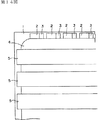
まず、第1図を参照して、本発明の有機EL表示装置における第1の実施形態について説明する。第1図は、本発明の有機EL表示装置の第1の実施形態を模式的に示したものであり、(a)は平面図、(b)はX−X線断面図、(c)はY−Y線断面図である。
1.基本的形態
第1図に示す本実施形態の有機EL表示装置は、支持基板1上に、下部電極(透明電極)2、有機発光層を含む有機層(以下、有機発光媒体という)4、および対向電極5をこの順に積層してなる有機EL表示装置であり、下部電極2と対向電極5がXYマトリックスを形成し、下部電極2と対向電極5の各交差部分が有機EL表示装置の発光部分(発光画素部分)8を構成している。
そして、支持基板1と下部電極2の間の対向電極5の下部に相当する部分に電気絶縁層6が設けてあり(第1図(c)参照)、この電気絶縁層6内に、下部電極2の抵抗値を減少させるための補助配線層3が埋設して配線してある。
本実施形態における補助配線層3は、電気絶縁層6内に埋設されることによって下部電極2と部分的に異なる面に配線され、かつ、有機EL表示装置の発光部分(発光画素部分)8と重ならないように非発光部に配線されるとともに、この非発光部において下部電極2に対して電気接続されて、下部電極2の抵抗値を減少させるように構成してある。
ここで、発光部分(発光画素部分)8とは、下部電極2と対向電極5とが交差する領域であり、かつ、有機発光媒体4に正孔または電子を注入できる領域である。また、非発光部分とは、下部電極2と対向電極5が交差していない領域であるか、または、下部電極2と対向電極5とが交差するものの、有機発光媒体4に正孔または電子を注入することができない領域である。
また、補助配線層3は、この非発光部、すなわち、各下部電極2の間に下部電極2と平行に配線され、対向電極5の下部に相当する部分は電気絶縁層6に埋設されるとともに(第1図(c)参照)、この下部電極2との平行配線部から各対向電極5の間隙に延びる配線部が対向電極5と平行に配線されていることを特徴としている。そして、補助配線層3は、対向電極5の間隙部において、下部電極2と電気接続している構成である(第1図(b)参照)。
また、電気絶縁層6は、支持基板1と下部電極2の間に形成される平坦化された絶縁層であり、内部に補助配線層3を埋設していることを特徴としている。
なお、電気絶縁層6は、第1図に示す補助配線層3のみを埋設する形態の他、第2図に示すように、表面に下部電極2を埋設し、下部電極2とともに表面を平坦化するように構成してもよい。このように構成すると、下部電極2の厚みに起因した段差も電気絶縁層6に埋設されることによって緩和され、対向電極5の断線や下部電極2と対向電極5との間の短絡もなくなる。すなわち、断線や、クロストーク等の表示欠陥をより低減させることができる。
さらに、電気絶縁層6の形態としては、第3図に示すように、下部電極2と補助配線層3との間に、ほぼ全面にわたって電気絶縁層6を形成し、補助配線層3をすべて電気絶縁層6に埋設することも好ましい。
このように構成すると、補助配線層3は、電気絶縁層6に埋設されることになり、すべての部分が下部電極2とは異なる面に配線されることになる。
なお、この場合、補助配線層3と下部電極2との間にすべて電気絶縁層6が存在することになるので、補助配線層3を下部電極2に電気接続するために、電気絶縁層6の有機EL表示装置の発光部分8と重ならない非発光部分にビアホール7を形成することができる。したがって、このビアホール7を介して補助配線層3と下部電極2を電気接続させることができる(第3図(b)参照)。
なお、このように構成しても、第1図の場合と同様に、下部電極2の抵抗値を有効に減少させることができる。
また、電気絶縁層6に形成するビアホール7は、第3図に示すように、対向電極5の間隙部に位置する電気絶縁層6と下部電極2とを連通する開口部となっている。そのため、ビアホール7内に、下部電極2と補助配線層3とを導通する導通部2aを配設することにより、下部電極2と補助配線層3とを電気的に接続することができる。
また、導通部2aとしては、下部電極2と補助配線層3とを電気的に接続するものであれば、部材の種類は特に制限されるものではなく、例えば、第3図(b)に示すように、スルーホール7に導電性部材を充填して導通部2aを形成してもよい。また、第4図に示すように、下部電極2の下面を延設することにより、下部電極2そのものを導通部2aとしてもよい。
なお、このようにビアホール7を設けることにより、補助配線層3の厚みの段差によって、下部電極2に断線が生ずることが少なくなる。したがって、下部電極2と補助配線層3とを確実に電気接続することができ、表示領域の輝度分布がより均一化するとともに、製造歩留まりを高くすることができる。
以上のような構成からなる本実施形態の有機EL表示装置によれば、補助配線層3および下部電極2の電気接続部が、有機EL表示装置における発光部分8と重なることがない。したがって、下部電極側から外部に取り出す光量を多くすることができ、結果として、有機EL表示装置の発光輝度の値を大きくすることができる。
また、補助配線層3と下部電極2との間には電気絶縁層6が設けてあるため、補助配線層3を電気絶縁層6内に埋設することができる。したがって、補助配線層3と下部電極2とが、それぞれ垂直方向に異なる面に配線される部分を有するため、補助配線層3が下部電極2の上に突出することがなくなり、装置各層を容易に平坦化することができる。また、このように構成することにより、補助配線層3の膜厚も問題とならない。
よって、このように構成することにより、製造上の歩留まりが向上して、クロストークや非発光ラインの発生等の表示欠陥をより少なくすることができる。
さらに、補助配線層3を埋設した電気絶縁層6を設けることにより、隣接する下部電極2と補助配線層3や下部電極2同士の電気絶縁性を十分に確保し、短絡等も生じず、補助配線層3の所要断面積を大きくすることができる。
2.構成要素
以下、本実施形態の有機EL表示装置を、その構成要素ごとにさらに具体的に説明する。
(1)下部電極
本実施形態では、下部電極は補助配線層と電気的に接続している。そして、補助配線層には、導電性の高い材料、すなわち低抵抗材料が使用されるため、下部電極層において導電性の高い材料を使用することは必須ではない。なお、下部電極側から外部へ光を取り出す場合は、発光波長において、光透過率が30%以上となるような導電材料を使用することが好ましい。
また、下部電極層は、有機EL素子の構成に対応して、陽極あるいは陰極となるが、下部電極層が陽極の場合は、正孔注入性に優れる高仕事関数(仕事関数4.0eV以上)の金属などの導電性物質を用いることが好ましい。また、陽極においては、抵抗率は問われないため、半導体を用いることもできる。具体的には、たとえば、金(Au),ニッケル(Ni),パラジウム(Pd),プラチナ(Pt)などの金属、In−Sn−O,ZnO:Al(ZnOにAlを添加した混合物),In−Zn−O,SnO2:Sb(SnO2、にSbを添加した混合物)などの導電性の酸化物、α−ケイ素,ポリシリコン,α−炭化ケイ素,α−炭素などの半導体を好適に用いることができる。更には、有機半導体である全共役系ポリマーも用いることができる。このようなポリマーとして、具体的には、ポリアニリン、ポリアリーレンビニレン、ポリチェニレンビニレン、ポリアセチレン、ポリピロールなどを好適に用いることがきる。
一方、下部電極層が陰極の場合は、電子注入性に優れる低仕事関数(仕事関数4.0eV以下)の金属、合金などの導電性物質を用いることが好ましい。また、陰極においても、抵抗率は問われないため、半導体を用いることもできる。
また、陰極に使用する合金としては、アルカリ土類金属、アルカリ金属または希土類金属を微量含有するもの、例えば、Al−Li,Al−Mg,Al−Ba,Al−Ca,Al−Sc,Al−Ybなどを好適に用いることができる。更には、BaO,SrO,MgOなどのアルカリ土類金属酸化物を超薄膜(20nm程度以下)にしたものも陰極として用いることができる。また、陰極の構成材料として、LaB6やTiNなどの低仕事関数のホウ化金属や、チッ化金属や、あるいは、低仕事関数の希土類シリサイドを用いることも好ましく、さらに有機発光媒体と前記金属との混合物を用いることも好ましい。
また、本実施形態においては、下部電極層は抵抗率が高くてもよいため、膜厚を薄くすることができる。その場合、膜厚を300nm以下の値、特に2〜200nmの範囲内の値とするのが好ましい。この場合において、膜厚が2〜10nmの範囲では、連続層が形成されない可能性がある。しかしながら、下部電極層と補助配線層を広い面積で密着させるような場合には、有機EL素子の動作上、支障がないことが判明している。
一方、膜厚が300nmより厚い場合には、下部電極層の段差部分において対向電極が断線したり、下部電極と対向電極が短絡する場合がある。
なお、本実施形態においては、下部電極は公知の方法により形成することができる。例えば、スパッタリング法により製膜し、その後フォトリソグラフィー法によりパターニングすることにより下部電極は形成される。
(2)補助配線層
本実施形態において、補助配線層は、下部電極の抵抗値を減少させる補助電線としての機能を有する。このため、低い抵抗値を有するとともに、下部電極と電気的に接続されている必要がある。
ここで、電気的接続とは、補助配線層と対向電極とに電源が接続された場合、有機EL表示装置に電圧が印加されるように補助配線層と下部電極とが接続されていることを意味する。したがって、補助配線層は、有機EL表示装置に供給される電流が流れるものであり、低い抵抗値を有するものが好ましい。すなわち、このような補助配線層を備えることにより、下部電極層の抵抗値を極めて低くすることができる。
また、本実施形態に用いる補助配線層としては、抵抗値が低いものであれば、特に制限はないが、たとえば、この補助配線層により低抵抗化された電極ライン(例えば 信号電極線)の抵抗値を5kΩ以下とするような金属線であることが好ましい。
この理由は、補助配線層と組み合わせた電極ラインの抵抗値が5kΩを超えると、画素の発光輝度ムラ、または有機EL表示装置の発光輝度ムラを発生する場合があるためである。
なお、テレビ画像表示を行う場合は、補助配線層と組み合わせて、電極ラインの抵抗値を1kΩ以下の値とすることがさらに好ましい。
また、信号電極線の長さが10cm程度の場合、信号電極線の単位長さ(1cm当たりの長さ)あたりの抵抗値としては、100Ω以下の値であることが好ましい。
また、補助配線層の抵抗率を、5×10⁻⁴Ω・cm以下の値とすることが好ましい。この理由は、補助配線層の抵抗率が5×10⁻⁴Ω・cmを超えると、補助配線層を設けることによる信号電極線の抵抗値の減少効果が期待できない場合があるためである。
このような補助配線層に用いられる金属としては、たとえばタングステン(W),アルミニウム(Al),銅(Cu),銀(Ag),モリブデン(Mo),タンタル(Ta),金(Au),クロム(Cr),チタン(Ti),ネオジウム(Nd),およびこれらの合金を挙げることができる。
また、これらの合金の具体例としては、Mo−W、Ta−W、Ta−Mo、Al−Ta、Al−Ti、Al−Nd、Al−Zr等の合金を挙げることができる。
更に、補助配線層の構成材料としては、金属とケイ素の化合物である、TiSi2,ZrSi2,HfSi2,VSi2,NbSi2,TaSi2,CrSi2,WSi2,CoSi2,NiSi2,PtSi,Pd2Siなども好ましい。また、これらの金属や・ケイ素化合物をそれぞれ積層した構成であってもよい。
なお、本実施形態に用いられる補助配線層に好ましく用いられる金属の抵抗率を表1に示す。

このような多層膜としては、上記金属またはそれらの合金を用いて形成することができる。たとえば、三層の場合、Ta層とCu層とTa層、およびTa層とAl層とTa層、二層の場合、Al層とTa層、Cr層とAu層、Cr層とAl層、およびAl層とMo層の組合わせを挙げることができる。
ここで、膜の安定性とは、低抵抗率を維持しうるとともに、エッチングの際、その処理に用いる液等により腐食されにくい性質をいう。たとえば、補助配線層をCuやAgで構成した場合には、補助配線層の抵抗率自体は低いものの、腐食しやすい場合がある。それに対して、CuやAgからなる金属膜の上部および下部、あるいはいずれか一方に、耐食性に優れた金属、たとえばTa,Cr,Mo等の膜を積層することにより、補助配線層の安定性を高めることができる。
また、補助配線層を金属膜として構成する場合、その膜厚を100nm〜数10μmの範囲内の値とすることが好ましく、特に好ましくは200nm〜5μmの範囲内の値とすることである。
この理由は、かかる膜厚が100nm未満となると、抵抗値が大きくなり、補助配線層として好ましくなく、一方、かかる膜厚が数10μmを超えると平坦化しにくくなり、有機EL表示装置の欠陥が生じるおそれがあるためである。
また、金属膜の幅(短辺の長さ)は、有機EL表示装置の精細度によるが、例えば、2μm〜1,000μmの範囲内の値とすることが好ましく、5μm〜300μmの範囲内の値とすることがより好ましい。
この理由は、かかる金属膜の幅が2μm未満となると、補助配線層の抵抗が大きくなる場合があるであり、一方、かかる金属膜の幅が100μmを超えると、EL先の外部への取り出しを妨害する場合があるためである。
(3)電気絶縁層
電気絶縁層は、下部電極と補助配線層とを電気絶縁するとともに、補助配線層のパターン縞の凸部を緩和するために設けられている。この電気絶縁層は、絶縁性材料からなる層であり、表面が平坦化してあることが好ましい。そして、電気絶縁層における平坦度は0.2μm以下の値であることが好ましい。
また、電気絶縁層の表面粗さは、発光欠陥の発生を抑制するため、10nm以下の値とすることが好ましい。
ここで、電気絶縁層の平坦度は、触針式膜厚計あるいは走査型原子間力顕微鏡等で測定される補助配線層におけるパターン縞の凹凸量と定義することができる。
一方、電気絶縁層の表面粗さは、電気絶縁層自体の表面における粗さ(凹凸)であり、500μm角〜1mm角の面積において触針式膜厚計等で測定される表面凹凸値の2乗平均値で定義される値である。
また、電気絶縁層の構成材料としては、所定の電気絶縁性を有する材料であれば、特に種類の制限はないが、例えば、2MV/cm以上の絶縁耐圧を有する材料が好ましい。
また、電気絶縁層は、下部電極を成膜する際の温度に耐えられる耐熱性を有する構成材料が好ましい。
また、電気絶縁層は、補助配線層を埋設する際や、補助配線層と下部電極とを電気的に接続するためのビアホールの加工を行う際に、微細なビアホールを形成するためにエッチング加工ができる構成材料であることが好ましい。
したがって、このような構成材料としては、たとえば透明性ポリマー、酸化物、ガラスなどを挙げることができる。
より具体的に言えば、好ましい透明性ポリマーとしては、ポリイミド,フッ素化ポリイミド,フッ素系樹脂,ポリアクリレート,ポリキノリン,ポリオキサジアゾール,環状構造を有するポリオレフィン,ポリアリレート,ポリカーボネート,ポリサルフォン,ラダー型ポリシロキサン等が挙げられる。
また、好ましい酸化物としては、SiO2,Al2O3,Ta2O3,Si3N4,フッ素添加SiO2,MgO,YbO3などを上記エッチング加工が可能な材料の好適例として挙げることができる。
さらに上述した電気絶縁層の構成材料に加えて、感光性を有するフォトレジストおよびその硬化物を挙げることができる。
ただし、有機EL素子は、水、酸素等により劣化しやすいため、含水量が0.1重量%以下、およびガス透過係数(JISK7126)が1×10⁻¹³cc・cm/cm2・s・cmHg以下の電気絶縁層材料を採用することが好ましい。よって、例えば無機酸化物、無機窒化物または両者の組成物が挙げられる。
また、電気絶縁層の膜厚としては、補助配線層を埋設することができるならば特に制限はないが、たとえば補助配線層の膜厚よりも厚く、かつ、10μm以下の値であることが好ましい。
(4)その他の構成要素
本実施形態の有機EL表示装置は、下部電極、補助配線層および電気絶縁層の他に、有機発光媒体、対向電極および支持基板を構成要素として含む。
このような有機EL表示装置において、下部電極と対向電極との間に介在する有機発光媒体は、少なくとも有機発光層を含むものであるが、有機発光層のみからなる単層であってもよい。また、有機発光媒体は、有機発光層とともに、正孔輸送層などを積層した多層構造であってもよい。
また、有機発光層に用いられる発光材料の種類についても特に制限はなく、従来の有機EL表示装置における公知のものを用いることができる。
例えば、有機発光層材料としては、オキシン金属錯体、スチルベン系色素、ポリフェニレンビニレン誘導体、DCM(シアニン色素)誘導体などを高水準の有機EL表示装置を与える材料として挙げることができる。
また、対向電極は、下部電極と対をなす電極であって、下部電極とは反対の電荷を有し、下部電極が陽極ならば陰極となり、逆に下部電極が陰極ならば陽極となる。そして、下部電極側から注入された電荷(正孔または電子)と対向電極側から注入された電荷(電子又は正孔)とが有機発光媒体において再結合し、有機EL表示装置の発光を生じることになる。
したがって、対向電極側から有機EL表示装置の発光を取り出す場合には、発光波長における光透過度が30%以上となるような対向電極を採用する必要がある。
このような構成材料としては、この種の有機EL表示装置の常用されているものをそのまま用いることができる。例えば、透明導電性酸化物膜、金属又は合金の膜厚20nm以下の超薄膜、あるいは透明導電性酸化物膜と前記超薄膜の積層膜等を挙げることができる。
そして、本実施形態において補助配線層の幅が、ピッチ幅(100%)に対して、100〜150%の場合には、対向電極側から取り出すことが好ましい。
また、支持基板は、機械的強度に優れ、水分や酸素の透過性が少ないものであれば、この種の有機エレクトルミネッセンス表示装置に常用されているものをそのまま用いることができる。具体的には、例えば、ガラスやセラミックス等を挙げることができる。また、蛍光変換膜、カラーフィルターが配設された基板を用いても良い。
[第2の実施形態]
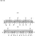
次に、第5図〜第7図を参照して、本発明の有機EL表示装置における第2の実施形態について説明する。第5図〜第7図は、有機EL表示装置の第2の実施形態を模式的に示した断面図であり、それぞれ(a)は、非発光部分(補助配線層と下部電極の接続部)、(b)は、発光部分の断面図である。
1.基本的形態
本実施形態の有機EL表示装置は、第1の実施形態と同様、支持基板1上に、下部電極2、有機発光媒体4、および対向電極5をこの順に積層してなる有機EL表示装置であり、下部電極2と対向電極5がXYマトリックスを形成し、下部電極2と対向電極5の各交差部分が発光部分8(第1図参照)を構成している。
そして、本実施形態では、下部電極2の抵抗値を減少させるための補助配線層3を下部電極2と同一面に配線するとともに、この補助配線層3と下部電極2との間に、電気絶縁層6が設けてある。
ここで、補助配線層は、下部電極と同一面、すなわち下部電極が配線される支持基板上に配線されており、第1の実施形態と同様、有機EL表示装置の発光部分と重ならない非発光部分に配線され、この非発光部分において下部電極の下側(または上側)に積層されて、下部電極と直接電気接続するように構成してある。
このように本実施形態では、第1の実施形態と異なり、下部電極と補助配線層がビアホールを介することなく直接積層されて電気接続されるようになっている。
そして、この電気接続部を除く下部電極と補助配線層との間には、電気絶縁層を設けることを特徴としている。
また、電気絶縁層は、少なくとも電気接続部を除く下部電極と補助配線層との間に設けられていればよく、その態様としては、例えば第5図〜第7図に示すものがある。
第5図では、発光部分8において隣接する各下部電極2の間に配線される補助配線層3の上面を覆うように電気絶縁層6が形成してある。
また、第6図では、第5図の形態に加えて、下部電極2と補助配線層3の接続部分上(非発光部分)にも電気絶縁層6が形成してある。
さらに、第7図では、各下部電極2および補助配線層3の隣接する間隙部に電気絶縁層6を充填して形成してある。
ここで、本実施形態の電気絶縁層についても、第1の実施形態の場合と同様に表面を平坦化することが好ましい。
以上のような構成からなる本実施形態の有機EL表示装置では、補助配線層および下部電極の電気接続部が、発光部分と重なっていないため、上述した第1の実施形態の場合と同様、下部電極側から外部に取り出す光量を多くすることができる。したがって、有機EL表示装置の発光輝度の値を大きくすることができる。
また、本実施形態では、同一平面に配線した下部電極と補助配線層との間には、電気接続部を除いて電気絶縁層が設けてあるので、下部電極と補助配線層との厚さ(膜厚)に起因する段差が電気絶縁層によって埋められる。これにより、従来生じていたような対向電極と下部電極の短絡によるクロストークや、対向電極の断線による表示欠陥、画面表示の不均一化等の発生を低減することができる。2.構成要素
上述した基本的形態を有する第2の実施形態の有機EL表示装置は、支持基板1、下部電極2、補助配線層3、有機発光媒体4、対向電極5および電気絶縁層6からなる谷構成要素の構成材料、形成方法等については、第1の実施形態と同様であるため、ここでの説明は省略するものとする。
[第3の実施形態]
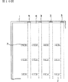
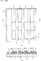
次に、本発明の第3の実施形態について第8図〜第14図を参照して説明する。第8図〜第14図は、第3の実施形態にかかる有機EL表示装置の製造方法の各工程における有機EL表示装置を模式的に示す概略説明図であり、平面図および断面図を含む。
1.基本的形態
第3の実施形態は、支持基板1上に、補助配線層3が電気接続された下部電極2と、有機発光媒体4と、対向電極5とを順次に設け、当該下部電極2および対向電極5をXYマトリックス状に配設した有機EL表示装置の製造方法であって、以下の工程を有することを特徴としている。
(1)補助配線層3と下部電極2とを、少なくとも部分的に異なる面に配線する工程
(2)補助配線層3を、下部電極2に対して、有機EL表示装置の非発光部分において電気接続する工程
このような各工程により、補助配線層および下部電極の電気接続部を発光部分以外の部分に容易に設けることができる。また、補助配線層を下部電極とは異なる面に配線しているため、容易に平坦化することができ、しかも、補助配線層の所要断面積を大きくすることもできる。
また、第3の実施形態を実施するにあたり、下部電極と補助配線層との間に電気絶縁層を設ける工程を含むことが好ましい。このように実施すると、補助配線層を電気絶縁層内に埋設して、平坦化することができるとともに、隣接する下部電極との電気絶縁性を十分に確保することができる。
また、第3の実施形態を実施するにあたり、有機EL表示装置の非発光部分にビアホールを設ける工程と、補助配線層を下部電極に対して、ビアホールを介して電気接続する工程を含むことが好ましい。
このように実施すると、補助配線層の厚みの段差に起因して、下部電極が断線することがなくなり、補助配線層と下部電極とを確実に電気接続することができる。
さらに、第3の実施形態を実施するにあたり、電気絶縁層の表面を平坦化する工程を含むことが好ましい。このように実施すると、補助配線層の膜厚が問題とならず、製造上の歩留まりが向上して、クロストークや表示欠陥をより少なくすることができる。
2.製造工程
以下、第3の実施形態の各工程を、第8図〜第14図を参照しつつ具体的に説明する。
なお、第3の実施形態は、第1の実施形態の有機EL表示装置を製造する方法であり、製造される有機EL表示装置の構成材料、構造は第1の実施形態と同様である。したがって、以下の説明は、第3の実施形態における特徴的な部分である補助配線層と電気絶縁層およびビアホールの形成方法について説明するものとし、その他の構成部分、例えば下部電極や、有機発光媒体等については、有機EL表示装置の分野における公知の製法を採ることができる。
まず、第8図(a)、(b)に示すように、支持基板1上にフォトリソグラフィー法またはリフトオフ法等を用いて補助配線層3のパターンを形成する。このとき、補助配線層3のパターンは、発光部分8と重ならない非発光部分に配線する。
次に、補助配線層3を被覆するようにして電気絶縁層6を形成する。このとき、電気絶縁層6は内部に補助配線層3を埋設して形成されるので、表面に補助配線層3が突出することなく、補助配線層3の凹凸を平坦化することができる。
また、電気絶縁層6の形成方法としては、スピンコート,ロールコート,蒸着,CVD,スパッタリング等によって電気絶縁層を成膜し、フォトリソグラフィー法を用いて任意の形状にパターニングする。または、成膜の際に任意の形状のマスクを用いて任意の形状に成膜することもでき、印刷手法を用いてもよい。
例えば、フォトレジストを用いて、パターニング、エッチングまたはリフトオフすることにより、第9図に示すような所定の位置(対向電極5の下部に相当する位置)に電気絶縁層6を形成する。
また、第3図で示したようなビアホール7を有する電気絶縁層6を形成する場合には、第10図に示すように、電気絶縁層6を支持基板1上のほぼ全面に形成するとともに、所定位置(有機EL表示装置の非発光部分に相当する位置)にビアホール7を形成する。
次に、第11図または第12図(第12図はビアホール7を設ける場合)に示すように、電気絶縁層6上に下部電極2を形成し、下部電極2と補助配線層6を接続する。
ここで、第12図に示すビアホール7を設ける場合は、ビアホール7を介して下部電極2と補助配線層3を接続する。具体的には、第13図(b)に示すように、ビアホール7内に導電性部材を充填して導通部2aを形成し、この導通部2aを介して下部電極2と補助配線層6を電気的に接続する。
なお、この場合、第1の実施形態の第4図で示したように、ビアホール7に下部電極2そのものを充填して補助配線層6と接続してもよい。
その後、第14図に示すように下部電極2上に有機発光媒体4を形成し、さらに対向電極5を下部電極2とXYマトリックスを構成するように形成する。
これによって、第1図(または第3図)に示したような、下部電極2と補助配線層3が発光部分8と重ならない非発光部分で電気接続された有機EL表示装置が完成する。
なお、補助配線層3および電気絶縁層6の形成方法として上記の方法を好適例として上げたが、特にこれに制限されるものではなく、他の製法を用いることもできる。
[第4の実施形態]
次に、本発明の第4の実施形態について説明する。この実施形態は、上述した第2の実施形態にかかる有機EL表示装置の製造方法である。
具体的には、支持基板1上に、補助配線層3が電気接続された下部電極2と、有機発光媒体4と、対向電極5とを順次に設け、当該下部電極2および対向電極5をXYマトリックス状に配設した有機EL表示装置の製造方法であって、以下の工程を有することを特徴としている。
(1)補助配線層3を、下部電極2と同一面に配線する工程
(2)有機EL表示装置の非発光部分において、補助配線層3を下部電極に対して電気接続する工程
(3)電気接続部を除く補助配線層3と下部電極の間に電気絶縁層6を設ける工程
このような各工程により、補助配線層3および下部電極2の電気接続部を発光部分8以外の部分に容易に設けることができる。
また、下部電極2と補助配線層3との間に電気絶縁層6を設けるようにしてあるので、補助配線層3を下部電極2と同一面に配線しても対向電極5との電気絶縁性を十分に確保することができる。
さらに、下部電極2と補助配線層3のそれぞれの膜厚に起因する段差を電気絶縁層6で埋めて平坦化することができ、補助配線層3の所要断面積を大きすることもできる。その結果、クロストークや非発光ラインの発生等の表示欠陥を低減することができる。
なお、本実施形態の各工程における製造方法は、上述した第3の実施形態における製造方法と同様である。
[第5の実施形態]
次に、第15図を参照して、第5の実施形態を説明する。第15図は、有機EL表示装置の第5の実施形態を模式的に示したものであり、(a)は平面図、(b)はX−X線断面図である。
なお、第5の実施形態は、第1の実施形態の有機EL表示装置で設けたビアホール7の開口形状を順テーパー状に製造するものであり、製造される有機EL表示装置の構成材料、構造は第1の実施形態と同様である。したがって、以下の説明では、第5の実施形態における特徴的な部分であるビアホール7の形状についてのものである。
1.基本的形態
第15図(a)、(b)に示すように、第5の実施形態は、電気絶縁層6におけるビアホール7の側面が、下部電極2に向かって広く、補助配線層3に向かって狭く傾斜する順テーパー状としてある。
このようにビアホール7を順テーパー状に構成すると、下部電極2が電気絶縁層6のエッジで断線することが少なくなる上に、ビアホール7の内部に対して、間口が広い部分から導電材料を容易に充填することができ、また、間口が広いため、補助配線層3と下部電極2との電気接続箇所における接触面積を大きくして、密着性を向上させることができ、表示領域の輝度分布を均一化することができる。
2.製造工程
第5の実施形態では、電気絶縁層6にビアホール7を形成する工程において、ビアホール7の側面を順テーパー状とする工程を有する。
このようにすると、例えば、蒸着法等を用いて、ビアホール内部に導電材料を容易に充填することができ、また、ビアホール内部に導電材料を充填した後に断線をより少なくすることができる。
順テーパー状のビアホール7の形成方法は、例えばパターン断面がオーバーハング形状となるレジストを形成した後、電気絶縁層6を成膜し、レジストを剥離(リフトオフ)することにより形成することができる。また、感光性レジストをビアホール形状のマスクで露光する際に、マスクと基板との距離を離して露光し、その後現像(必要に応じて焼成)することによっても形成できる。
なお、他の製造工程や、形成方法は、第3の実施形態と同様とすることができる。
[第6の実施形態]
さらに、第16図を参照して、第6の実施形態を説明する。第16図は、有機EL表示装置の第6の実施形態を模式的に示した平面図である。
この第6の実施形態は、第1または第2の実施形態の有機EL表示装置における補助配線層3の配線パターンを変更したものであり、その他の構成材料、構造、形成方法等は第1〜第4の実施形態と同様である。したがって、以下の説明では、第6の実施形態における特徴的な部分である補助配線層3の配線パターンについてのものである。
第6の実施形態の補助配線層3は、配線パターンが有機EL表示装置の発光部8と重ならない非発光部分に配線され、各下部電極2に沿って形成された梯子形状をなす配線パターンとなっている。
第16図に示すように、補助配線層3は、各下部電極2(第16図では図示省略)の間に沿って平行に配線されるとともに、この平行配線部分が対向電極5(第16図では図示省略)の間隙に沿って形成される配線パターンで連結され、各下部電極2ごとに対応した梯子形状となっている。
このように補助配線層3を梯子形状の配線パターンに形成することによって、発光部分と干渉することなく補助配線層3の所要断面積を広くすることができ、配線抵抗の減少効率をより向上させるとともに、抵抗率の調整範囲値も広く確保することができるので、表示領域の輝度の均一性をより向上させることができる。
実施例
[実施例1]
(1)有機EL表示装置の製造
▲1▼補助電極の形成
実施例1の有機EL表示装置を製造するにあたっては、まず、厚さ1.1mm、縦100mm、横100mmのガラス基板OA2(日本電気硝子(株)製)上に、補助電極材料であるアルミニウムを膜厚が200nmとなるように成膜した。
このガラス基板上に、ポジ型レジストHPR204(富士フィルムオーリン(株)製)をスピンコートし、フォトマスクを介して紫外線を露光した後、現像液としてTMAH(テトラメチルアンモニウムヒドロキシド)を用いて、露光部を現像した。
次いで、オーブンを用いて、130℃、10分の条件でポストベーク処理した後、アルミニウムエッチャント(酢酸/リン酸/硝酸)を用いて、アルミニウム膜をエッチングした。
その後、剥離液N303(長瀬産業(株)製)を用いてポジ型レジストを除去し、第8図に示すパターンを有する補助配線層を形成した。
▲2▼電気絶縁層の形成
次いで、補助配線層を形成した基板上に、ネガ型レジストIC28T−3(富士フィルムオーリン(株)製)をスピンコートし、フォトマスクを介して紫外線を露光した後、現像液としてキシレンを用いて、未露光部を現像した。
その後、160℃、10分の条件でポストベーク処理し、レジストパターンを得た。このレジストパターンの上からSiO2をスパッタリングして、膜厚200nmの電気絶縁層とした。その後、剥離液N303を用いてネガ型レジストを除去し、第9図に示すように、電気絶縁層のパターンをリフトオフ法によって補助配線層上に形成した。
▲3▼下部電極の形成
次いで、電気絶縁層を形成した基板上に、IZO(インジウム亜鉛酸化物)をスパッタリングして、電気絶縁層上に、膜厚120nmのIZO膜を形成した。
このIZO膜上に、ポジ型レジストHPR204をスピンコートし、フォトマスクを介して紫外線を露光した後、TMAHにより露光部を現像した。
次いで、オーブンを用いて、130℃、10分の条件でポストベーク処理した後、IZOエッチャント(5%蓚酸水溶液)を用いて、ポジ型レジストから露出しているIZO膜をエッチングした。
その後、剥離液N303を用いてポジ型レジストを除去し、第11図に示すパターンを有する下部電極を形成した。
▲4▼有機EL素子の形成
下部電極を形成した基板をイソプロピルアルコール洗浄し、さらに紫外線洗浄を行った。この時点で、下部電極表面を、XPSを用いて表面観察したところ、炭素含有量が10atm%未満の値であることを確認した。
次いで、下部電極を形成して洗浄した基板を、蒸着装置(日本真空技術(株)製)内の基板ホルダーに固定した。
そして、蒸着装置内のモリブテン製の加熱ボードに、以下の材料をそれぞれ充填した。
正孔注入材料:4,4’,4”−トリス[N−(3−メチルフェニル)−N−
フェニルアミノ]トリフェニルアミン(MTDATA)、および
4,4’−ビス[N−(1−ナフチル)−N−フェニルアミノ]
ビフェニル(NPD)
有機発光材料:4,4’−ビス(2,2−ジフェニルビニル)ビフェニル
(DPVBi)
電子注入材料:トリス(8−キノリノール)アルミニウム(Alq)
さらに対向電極(陰極)材料としての銀ワイヤーをタングステン製フィラメントに、同じくマグネシウムリボンをモリブテン製の加熱ボードに装着した。
その状態で、真空層の真空度を665X10−7Pa(IX10−7Torr)まで減圧し、以下の蒸着速度および膜厚となるように、正孔注入層から陰極の形成まで、途中で真空状態を破らず、一回の真空引きで順次積層し、第1図および第14図に示すような有機EL素子を形成し、実施例1の有機EL表示装置とした。
なお、対向電極の銀およびマグネシウムは、それぞれ同時蒸着し、合わせて膜厚が200nmとなるように成膜した。
MTDATA:蒸着速度0.1−0.3nm/sec.,膜厚60nm
NPD :蒸着速度0.1−0.3nm/sec.,膜厚20nm
DPVBi :蒸着速度0.1−0.3nm/sec.,膜厚50nm
Alq :蒸着速度0.1−0.3nm/sec.,膜厚20nm
Ag :蒸着速度1.3−1.4nm/sec.,膜厚200nm
(AgとMgとの合計膜厚)
Mg :蒸着速度0.1nm/sec.
(2)有機EL表示装置の評価
得られた有機EL表示装置において、下部電極(陽極)と、対向電極である上部電極(陰極)との間に、DC12Vの電圧を印加し、各電極の交差部分の画素を発光させた。
その状態で色彩色差計CS100(ミノルタ(株)製)を用いて発光輝度を測定したところ、300cd/m2という値が得られた。また、JIS Z 8701に準拠してCIE色度座標を測定したところ、CIEx=0.14,CIEy=0.20である青色の強い発光が得られることを確認した。
さらにまた、得られた有機EL表示装置において、クロストークはほとんど見られず、隣接するラインの発光や欠陥表示についても240本中、1本も観察されなかった。
[実施例2]
(1)有機EL表示装置の製造
実施例1と同一の条件で補助配線層を形成した基板を作製した。
次いで、ネガ型レジストIC28T−3(富士フィルムオーリン(株)製)をスピンコートし、フォトマスクを介して紫外線を露光した後、現像液としてキシレンを用いて、未露光部を現像した。その後、160℃、10分の条件でポストベーク処理し、レジストパターンを得た。このレジストパターンの上からSiO2をスパッタリングして、膜厚200nmの電気絶縁層とした。
次いで、剥離液N303を用いてネガ型レジストを除去し、第10図に示すように、電気絶縁層に囲まれたビアホールを補助配線層上に形成した。なお、ビアホールの外観をSEM(Scanning Electron Microscopy,電子顕微鏡)を用いて観察したところ、ビアホールの断面が矩形状であることを確認した。
以下、実施例1と同一の条件により(なお、下部電極の形成工程については第12図、第13図参照)、第3図に示す有機EL表示装置を作製した。
(2)有機EL表示装置の評価
得られた有機EL表示装置において、下部電極(陽極)と、対向電極である上部電極(陰極)との間に、DC12Vの電圧を印加し、各電極の交差部分の画素を発光させた。色彩色差計CS100(ミノルタ(株)製)を用いて発光輝度を測定したところ、300cd/m2という値が得られた。また、JIS Z 8701に準拠してCIE色度座標を測定したところ、CIEx=0.14,CIEy=0.20である青色の強い発光が得られることを確認した。
さらにまた、得られた有機EL表示装置において、クロストークはほとんど見られず、隣接するラインの発光や欠陥表示についても240本中、1本も観察されなかった。
[実施例3]
(1)有機EL表示装置の製造
実施例2における矩形状のビアホールの代わりに、順テーパー状のビアホール(第15図参照)を形成したほかは、実施例1と同様に有機EL表示装置を製造した。すなわち、補助配線層を形成した基板上に、パターン断面がオーバーハング形状となるネガ型レジストZPN1100(日本ゼオン(株)製)を用いたほかは、実施例2と同様に有機EL表示装置を製造した。なお、ビアホールの外観を、SEMを用いて観察し、ビアホールの断面が順テーパー状であることを確認した。
(2)有機EL表示装置の評価
得られた有機EL表示装置において、下部電極(陽極)と、対向電極である上部電極(陰極)との間に、DC12Vの電圧を印加し、各電極の交差部分の画素を発光させた。色彩色差計CS100を用いて発光輝度を測定したところ、300cd/m2という値が得られた。なお、下部電極と、上部電極とをそれぞれ選択して発光させたが、全表示領域(画素数約6万(240本×240本))における輝度分布は、±10cd/m2の範囲内であり、均一に発光することを確認した。
また、JIS Z 8701に準拠してCIE色度座標を測定したところ、CIEx=0.14,CIEy=0.20である青色の強い発光が得られることを確認した。
さらにまた、得られた有機EL表示装置において、クロストークはほとんどみられず、隣接するラインの発光や欠陥表示についても240本中、1本も観察されなかった。
[実施例4]
(1)有機EL表示装置の製造
実施例2における電気絶縁層であるSiO2の代わりに、アクリル系ネガ型レジストを使用したほかは、実施例2と同様に有機EL表示装置を製造した。
すなわち、補助配線層を形成した基板上に、アクリル系ネガ型レジストV259PA(新日鉄化学(株)製)をスピンコートし、フォトマスクと基板のギャップ(プロキシミティーギャップ500μm)をとって紫外線を露光した後、現像液としてTMAHを用いて、未露光部を現像し、180℃、10分の条件でポストベーク処理し、膜厚200nmの電気絶縁層とした。
(2)有機EL表示装置の評価
得られた有機EL表示装置において、下部電極(陽極)と、対向電極である上部電極(陰極)との間に、DC12Vの電圧を印加し、各電極の交差部分の画素を発光させた。色彩色差計CS100を用いて発光輝度を測定したところ、300cd/m2という値が得られた。なお、下部電極と、上部電極とをそれぞれ選択して発光させたが、全表示領域における輝度分布は、±10cd/m2の範囲内で均一に発光することを確認した。
また、JIS Z 8701に準拠してCIE色度座標を測定したところ、CIEx=0.14,CIEy=0.20である青色の強い発光が得られることを確認した。
さらに、得られた有機EL表示装置において、クロストークはほとんどみられず、隣接するラインの発光や欠陥表示についても240本中、1本も観察されなかった。
[実施例5]
(1)有機EL表示装置の製造
実施例5の有機EL表示装置の製造にあたっては、実施例1と同様のガラス基板OA2(日本電気硝子(株)製)からなる支持基板上に、アルミニウムをスパッタリングにより膜厚200nmとなるように成膜後、さらにクロムをスパッタリングにより膜厚50nmとなるように積層した。
次に、この支持基板上に、ポジ型レジストHPR204(富士フィルムオーリン(株)製)をスピンコートし、フォトマスクを介して紫外線を露光し、TMAH(テトラメチルアンモニウムヒドロキシド)を現像液として用いて露光部を現像し、130℃、10分の条件でポストベーク処理した。
その後、硝酸セリウムアンモニウム/過塩素酸水溶液からなるクロムエッチャントHCE(長瀬産業(株)製)と、酢酸/リン酸/硝酸からなるアルミニウムエッチャントを用いて、露出している部分のクロムおよびアルミニウム膜をエッチングした後、剥離液N303(長瀬産業(株)製)を用いてポジ型レジストを除去し、第8図に示すパターン形状のクロム/アルミニウムパターンからなる補助配線層を形成した。
次いで、この補助配線層を形成した基板上に、ITO(インジウム錫酸化物)をスパッタリングにより120nmの膜厚となるように成膜した後、さらにクロムをITO上にスパッタリングにより積層した。
そして、この基板上に上述したのと同様のポジ型レジストをスピンコートし、補助配線層に対して、第11図に示すような下部電極形状に対応する位置決めがなされたフォトマスクを介して紫外線を露光し、さらに、現像液としてTMAHを用いて現像し、130℃、10分の条件でポストベーク処理した。
次に、上述と同様の硝酸セリウムアンモニウム/過塩素酸水溶液からなるクロムエッチャントと、47%臭化水素水溶液からなるITOエッチャントを用いて、レジストから露出しているクロム/ITO層をエッチングし、その後、上述と同様の剥離液を用いてポジ型レジストを除去した。
これによって、第11図に示す下部電極に対応したクロム/ITOパターン層を形成した(なお、本実施例では、第11図に示した電気絶縁層6は存在しない)。
次に、このクロム/ITOパターン層を形成した基板上に、アクリル系ネガ型レジストV259PA(新日鉄化学(株)製)をスピンコートし、支持基板側から背面露光(バックフラッシュ)した後、現像液にて未露光部分を現像し、180℃、10分の条件でポストベーク処理し、これにより電気絶縁層を形成した。 その後、クロム/ITOパターン(下部電極に相当)上のクロムと、補助配線層上のクロムを、クロムエッチャントを用いて剥離し、ITOパターンからなる下部電極およびアルミニウムパターンからなる補助配線層を形成するとともに、この下部電極および補助配線層の間に電気絶縁層を充填形成した(第7図参照)。以下、実施例と同一の条件により、第7図に示す電気絶縁層を備えた有機EL表示装置を作製した。
(2)有機EL表示装置の評価
得られた有機EL表示装置において、下部電極(陽極)と、対向電極である上部電極(陰極)との間に、DC12Vの電圧を印加し、各電極の交差部分の画素を発光させた。色彩色差計CS100を用いて発光輝度を測定したところ、300cd/m2という値が得られた。
また、JIS Z 8701に準拠してCIE色度座標を測定したところ、CIEx=0.14,CIEy=0.20である青色の強い発光が得られることを確認した。
さらにまた、得られた有機EL表示装置において、クロストークはほとんど見られず、隣接するラインの発光や欠陥表示についても240本中、1本も観察されなかった。
[比較例1]
(1)有機EL表示装置の製造
比較例1の有機EL表示装置の構造は、実施例1において補助配線層と下部電極とを直接電気接合するとともに、当該電気接合箇所を、有機EL表示装置の発光部分の側部、すなわち、下部電極の端辺上に補助配線を積層して設け、当該電気接合箇所上を覆うように電気絶縁層を設けたほかは、実施例1と同様に有機EL表示装置を製造した(第18図参照)。
(2)有機EL表示装置の評価
得られた有機EL表示装置において、下部電極と、対向電極との間に、DC12Vの電圧を印加し、各電極の交差部分の画素を発光させた。色彩色差計CS100を用いて発光輝度を測定したところ、250cd/m2という、実施例1の発光輝度よりも低い値が得られた。
この原因としては、比較例1では、補助配線層と、下部電極とが一部重なっているため、外部に取り出せる発光量が減少したためと思われる。
なお、比較例1でも、CIE色度座標については、CIEx=0.14,CIEy=0.20であり、青色の発光が得らることを確認した。
また、得られた有機EL表示装置において、クロストークが10箇所以上発生し、これに起因して隣接するラインの発光や、断線による欠陥表示(非発光ライン)が240本の画素のうち、15本に見られることが確認された。これは、下部電極と同一平面上に配線された補助電極が、下部電極の端辺に重なるように形成されているため、下部電極と補助電極との膜厚や、積層高さに起因する段差がより顕著となり、その結果、下部電極と対向電極との間での短絡や、対向電極の断線が生じたためと考えられる。
[比較例2]
(1)有機EL表示装置の製造
比較例2の有機EL表示装置の構造は、電気絶縁層を設けず、補助配線層と、下部電極とをすべて同一面内に形成して、直接電気接合したほかは、実施例1と同様に有機EL表示装置を製造した(第17図参照)。
(2)有機EL表示装置の評価
得られた有機EL表示装置において、下部電極と、対向電極との間に、DC12Vの電圧を印加し、各電極の交差部分の画素を発光させた。色彩色差計CS100を用いて発光輝度を測定したところ、300cd/m2という値が得られた。また、CIE色度座標については、CIEx=0.14,CIEy=0.20であり、青色発光であることを確認した。
また、得られた有機EL表示装置において、クロストークが10箇所以上発生し、隣接するラインの発光や、断線による欠陥表示(非発光ライン)が240本中、10本あることが確認された。
このクロストークの大量発生や欠陥表示の増加の原因としては、補助配線層と下部電極とが同一平面にあるため、これらの厚さ(膜厚)に起因した段差が大きくなり、またその段差を有する頻度が増えたので、対向電極と下部電極、あるいは対向電極と補助配線層との短絡または対向電極の断線が生じたためと考えられる。
以上、詳細に説明したように、本発明の有機EL表示装置(第1の発明)によれば、補助配線層と下部電極とが、少なくとも異なる面に配線された部分を有するとともに、補助配線層を、有機EL表示装置の非発光部分において電気接続することにより、発光輝度の値が大きくなり、補助配線層の膜厚が問題とならず、しかも補助配線層の所要断面積が大きく、発光輝度の均一性が高く、消費電力を小さくできるとともに、表示欠陥の少ない高品質の有機EL表示装置を提供することができるようになった。
また、本発明の有機EL表示装置(第2の発明)によれば、補助配線層と、下部電極とを同一面に配線し、有機EL表示装置の非発光部分において補助配線層と、下部電極とを電気接続するとともに、補助配線層と下部電極との間であって、電気接続部を除いた箇所に電気絶縁層を設けることにより、補助配線層および下部電極の電気接続部が、発光部分と重なっていないため、下部電極側から外部に取り出す光量を多くすることができ、結果として、発光輝度の値が大きく、表示欠陥の少ない高品質の有機EL表示装置を提供することができるようになった。
また、本発明の有機EL表示装置の製造方法(第3の発明)によれば、補助配線層と下部電極とを部分的に異なる面に配線する工程と、補助配線層を、下部電極に対して、有機EL表示装置の非発光部分において電気接続する工程と、を含むことにより、補助配線層および下部電極の電気接続部を、発光部分以外に容易に設けることができるようになり、また、補助配線層と下部電極とを、それぞれ垂直方向に異なる面に配線しているため、容易に平坦化することができ、しかも、補助配線層の所要断面積を大きくした場合であっても、クロストークや非発光ラインの発生等の表示欠陥を低減できるようになった。
また、本発明の有機EL表示装置の製造方法(第4の発明)によれば、補助配線層と、下部電極とを同一面に配線する工程と、有機EL表示装置の非発光部分において、補助配線層を下部電極に対して電気接続する工程と、補助配線層と下部電極の間であって、電気接続部を除いた箇所に電気絶縁層を設ける工程と、を含むことにより、補助配線層および下部電極の電気接続部を、発光部分以外に容易に設けることができるようなった。また、このように実施することにより、下部電極と補助配線層の膜厚に起因する段差を電気絶縁層で埋めて平坦化することができるため、補助配線層の所要断面積を大きくした場合であっても、クロストークや非発光ラインの発生等の表示欠陥が低減できるようになった。
【図面の簡単な説明】
第1図は、第1の実施形態における有機EL表示装置を模式的に示す概略説明図であり、(a)は平面図、(b)はX−X線断面図、(c)はY−Y線断面図である。
第2図は、第1の実施形態における有機EL表示装置の他の形態を模式的に示した発光部分の断面図である。
第3図は、第1の実施形態における有機EL表示装置の他の形態を模式的に示す概略説明図であり、(a)は平面図、(b)はX−X線断面図、(c)はY−Y線断面図である。
第4図は、第1の実施形態における有機EL表示装置のさらに他の形態を模式的に示した非発光部分の断面図である。
第5図は、第2の実施形態における有機EL表示装置を模式的に示した断面図であり、(a)は非発光部分、(b)は発光部分の断面図である。
第6図は、第2の実施形態における有機EL表示装置の他の形態をを模式的に示した断面図であり、(a)は非発光部分、(b)は発光部分の断面図である。
第7図は、第2の実施形態におけるさらに有機EL表示装置のさらに他の形態を模式的に示した断面図であり、(a)は非発光部分、(b)は発光部分の断面図である。
第8図は、第3の実施形態における製造方法の補助配線層形成工程における有機EL表示装置を模式的に示す概略説明図であり、(a)は平面図、(b)はX−X線断面図である。
第9図は、第3の実施形態における製造方法の電気絶縁層形成工程における有機EL表示装置を模式的に示す概略平面図である。
第10図は、第3の実施形態における製造方法の電気絶縁層形成工程における有機EL表示装置を模式的に示す概略平面図である。
第11図は、第3の実施形態における製造方法の下部電極形成工程における有機EL表示装置を模式的に示す概略平面図である。
第12図は、第3の実施形態における製造方法の下部電極形成工程における有機EL表示装置を模式的に示す概略平面図である。
第13図は、第3の実施形態における製造方法の下部電極形成工程における有機EL表示装置を模式的に示す概略説明図であり、(a)は平面図、(b)はX−X線断面図である。
第14図は、第3の実施形態における製造方法の有機発光媒体および対向電極形成工程における有機EL表示装置を模式的に示す概略平面図である。
第15図は、第5の実施形態における有機EL表示装置の電気絶縁層を模式的に示す概略説明図であり、(a)は平面図(b)はX−X線断面図である。
第16図は、第6の実施形態における有機EL表示装置の補助配線パターンを模式的に示す概略平面図である。
第17図は、従来の補助電極を備えたEL素子を模式的に示す概略説明図であり、(a)は補助電極と第1電極の積層部の断面図、(b)は補助電極の配線部の断面図である。
第18図は、従来の透明電極の周囲に金属電極を備えた有機EL素子を模式的に示す概略断面図である。
第19図は、従来の補助配線層を備えた有機EL表示装置を模式的に示す概略断面図である。TECHNICAL FIELD The present invention relates to an organic electroluminescence display device (hereinafter sometimes referred to as an organic EL display device) and a method for manufacturing the same.
More particularly, the present invention relates to an organic EL display device having a large light emitting pixel area and a manufacturing method for efficiently obtaining such an organic EL display device, which are suitable for consumer and industrial display devices (displays).
2. Description of the Related Art Conventionally, there has been proposed an EL display device in which an EL element configured by sandwiching a light emitting layer between electrodes is driven (light emission) through scanning electrode lines and signal electrode lines arranged in a matrix. In order to increase the definition of a pixel, it is required to prevent a voltage drop or a response delay due to a wiring resistance such as a scanning electrode line.
For this reason, as shown in FIG. 17, an inorganic EL in which a first transparent electrode (lower electrode) 102, an inorganic
As an EL element provided with this kind of auxiliary electrode, there is an EL element disclosed in JP-A-8-180974.
Further, in Japanese Patent Application Laid-Open No. 11-31590, as shown in FIG. 18, each
On the other hand, as shown in FIG. 19, WO97 / 34447 discloses an organic EL element in which a
However, in the EL element shown in FIG. 17, the first transparent electrode (lower electrode) and the auxiliary electrode are wired on the same plane and are electrically connected in a state where they overlap each other, and directly on the transparent electrode and the auxiliary electrode. Since the light emitting layer is laminated, there are many places where a step due to the film thickness of the transparent electrode and the auxiliary electrode occurs. For this reason, a display defect such as a crosstalk in which a pixel other than the selected pixel emits light due to a short circuit between the counter electrode and the lower electrode, or a non-light emitting line in which the selected pixel does not emit light due to the disconnection of the counter electrode. There was a problem that was likely to occur.
In addition, since the transparent electrode and the auxiliary electrode are formed in the same plane, the required cross-sectional area of the auxiliary electrode itself is reduced, and the high definition of the light emitting pixel cannot be sufficiently handled. In particular, when the luminescent pixel is made high-definition, for example, when the resistance value of the transparent electrode becomes a value of 1 kΩ or more, the width and film thickness of the auxiliary electrode are changed to reduce the resistance value of the transparent electrode. For example, it was not easy to adjust to a value of 100Ω or less.
Furthermore, since the transparent electrode and the auxiliary electrode are formed in the same plane, when the transparent electrode and the auxiliary electrode are misaligned, adjacent transparent electrodes are short-circuited via the misaligned auxiliary electrode and displayed. Due to the occurrence of defects, there was a problem that the manufacturing yield was lowered.
In the case of the organic EL element shown in FIG. 18, since the metal electrode is covered with an insulating layer, the problem that the transparent electrode is short-circuited due to the displacement of the metal electrode can be avoided. Since the metal electrode wired above is formed so as to overlap the edge of the transparent electrode, the difference in level due to the film thickness and stacking height between the transparent electrode and the metal electrode becomes more prominent. There was a problem that a short circuit occurred between the counter electrode and display defects such as crosstalk and non-light emitting lines were more likely to occur than in the case of the EL element shown in FIG.
In addition, in the case of such an organic EL element, the metal electrode is configured to be electrically connected only on the four sides of the transparent electrode on the same plane as the transparent electrode and not affecting the light emitting region of the EL element. However, since the transparent electrode is covered with the metal electrode, there is a problem that when the required sectional area of the metal electrode is increased, the light emission area is reduced. As a result, there has been a problem that when the light emitting pixel is made high definition, the light emission luminance cannot be sufficiently obtained.
On the other hand, in the organic EL display device disclosed in PCTWO 97/3447, the auxiliary wiring layer is embedded in a flattening layer or the like, so that there is no problem with the step caused by the film thickness of the auxiliary wiring layer. There are advantages in that the manufacturing yield is high and display defects such as crosstalk and non-light emitting lines are small. However, since the electrical connection portion between the auxiliary wiring layer and the lower electrode is provided at the side end of the lower electrode, it is difficult to increase the required cross-sectional area of the auxiliary electrode. There was a problem that decreased.
Accordingly, the inventors of the present invention diligently studied the above problem, and as a result, the auxiliary wiring layer was partially wired on a surface different from the lower electrode, and the auxiliary wiring layer was electrically connected to the non-light emitting portion of the organic EL display device. By connecting, even when the auxiliary wiring layer and the lower electrode are wired on the same surface, an electrical insulating layer is provided between the lower electrode and the auxiliary wiring layer to make electrical connection in the non-light emitting portion. It was found that each can solve the conventional problems.
That is, the object of the present invention is that the area of the light emitting pixel is large, the adverse effects such as the occurrence of display defects due to the film thickness of the auxiliary wiring layer can be eliminated, the required cross-sectional area of the auxiliary wiring layer can be increased, and the light emission luminance can be increased. The object is to provide a high organic EL display device.
Another object of the present invention is to provide a manufacturing method capable of manufacturing an organic EL display device having a large light emitting pixel area and eliminating adverse effects such as generation of display defects due to the film thickness of the auxiliary wiring layer with high yield. There is to do.
DISCLOSURE OF THE INVENTION [1] One aspect of the present invention (first invention) is that a lower electrode, an organic light-emitting medium, and a counter electrode, which are electrically connected to an auxiliary wiring layer, are sequentially provided on a support substrate. In the organic EL display device in which the lower electrode and the counter electrode are arranged in an XY matrix, the auxiliary wiring layer and the lower electrode are wired on different surfaces, and the auxiliary wiring layer and the lower electrode are connected to each other in the organic EL display device. This is an organic EL display device electrically connected in the light emitting portion.
With this configuration, since the electrical connection portion and the light emitting portion do not overlap, the amount of light extracted from the lower electrode side can be increased, and as a result, the light emission luminance value of the organic EL display device is increased. be able to.
In addition, since the auxiliary wiring layer and the lower electrode are wired on different surfaces in the vertical direction, it can be easily flattened, and adverse effects such as occurrence of a short circuit due to the film thickness of the auxiliary wiring layer can be eliminated. Can do.
Furthermore, since the problem of short circuit between adjacent lower electrodes or between the lower electrode and the counter electrode does not occur, the thickness or width of the auxiliary wiring layer can be increased and the required cross-sectional area can be increased. In addition, the driving voltage (power consumption) of the organic EL display device can be reduced, and display defects such as generation of crosstalk and non-light emitting lines can be reduced.
[2] In configuring the organic EL display device of the first invention, it is preferable to provide an electrical insulating layer between the auxiliary wiring layer and the lower electrode.
If comprised in this way, since an auxiliary wiring layer can be embed | buried in an electrical insulating layer, even if it is a case where an auxiliary wiring layer is provided, the surface can be planarized. Therefore, sufficient electrical insulation can be ensured between adjacent lower electrodes or between the lower electrode and the counter electrode.
[3] Further, in configuring the organic EL display device according to the first aspect of the invention, it is preferable that the auxiliary wiring layer and the lower electrode are electrically connected through a via hole provided in a non-light emitting portion of the organic EL display device.
With this configuration, the lower electrode is less likely to be disconnected due to the step difference in the thickness of the auxiliary electrode, and the auxiliary electrode and the lower electrode can be reliably electrically connected.
[4] In another aspect of the present invention (second invention), a lower electrode electrically connected to the auxiliary wiring layer, an organic light emitting medium, and a counter electrode are sequentially provided on a support substrate, In the organic EL display device in which the lower electrode and the counter electrode are arranged in an XY matrix, the auxiliary wiring layer and the lower electrode are wired on the same surface, and the auxiliary wiring layer and the lower electrode are electrically connected in the non-light emitting portion. And an electrical connection, and an organic EL display device in which an electrical insulating layer is provided between the auxiliary wiring layer and the lower electrode, excluding the electrical connection portion.
With this configuration, since the electrical connection portion of the auxiliary wiring layer and the lower electrode does not overlap with the light emitting portion, the amount of light extracted from the lower electrode side can be increased, and as a result, the organic EL display device The value of the emission luminance can be increased.
In addition, since an electrical insulating layer is formed between the lower electrode and the auxiliary wiring layer wired on the same plane, except for the electrical connection portion, the step due to the film thickness of the lower electrode and the auxiliary wiring layer is electrically insulated. It is filled with the layer, so that the short circuit between the counter electrode, the lower electrode and the auxiliary wiring layer and the disconnection of the counter electrode do not occur. Therefore, display defects such as crosstalk and generation of non-light emitting lines can be reduced.
[5] In configuring the organic EL display devices of the first and second inventions, it is preferable that the surface of the electrical insulating layer is flattened.
With this configuration, the film thickness of the auxiliary wiring layer does not become a problem, the manufacturing yield is improved, and display defects such as the occurrence of crosstalk and non-light emitting lines can be reduced.
[6] In configuring the organic EL display devices of the first and second inventions, it is preferable that the side surface of the via hole for electrically connecting the auxiliary wiring layer and the lower electrode has a forward tapered shape. .
With this configuration, the lower electrode is less likely to be disconnected at the edge of the electrical insulating layer, and can be more reliably electrically connected to the auxiliary wiring layer. Moreover, since it is comprised in this way, since a frontage is wide, the contact area in the electrical connection location of an auxiliary wiring layer and a lower electrode can be enlarged, and adhesiveness can be improved. Furthermore, the inside of the via hole can be easily filled with, for example, a conductive material from a portion having a wide opening, and can be easily manufactured.
[7] In configuring the organic EL display devices of the first and second inventions, it is preferable that a lower electrode is extended and electrically connected inside the via hole of the electrical insulating layer.
For example, by filling the inside of the via hole with the same conductive material as that of the lower electrode or the auxiliary wiring layer and extending the lower electrode, the electrical connection between the lower electrode and the auxiliary wiring layer becomes more reliable.
[8] Further, according to still another aspect (third invention) of the present invention, a lower electrode, an organic light emitting medium, and a counter electrode, to which an auxiliary wiring layer is electrically connected, are sequentially provided on a support substrate, In the method of manufacturing an organic EL display device in which the lower electrode and the counter electrode are arranged in an XY matrix,
Wiring the auxiliary wiring layer and the lower electrode on partially different surfaces;
Electrically connecting the auxiliary wiring layer and the lower electrode by forming an electrical connection in the non-light emitting portion;
It is the manufacturing method of the organic electroluminescence display characterized by including these.
By carrying out in this way, the electrical connection part of the auxiliary wiring layer and the lower electrode can be easily provided in addition to the light emitting part of the organic EL display device. Further, since the auxiliary wiring layer and the lower electrode are wired on different surfaces in the vertical direction, it can be easily flattened. In addition, since the required cross-sectional area of the auxiliary wiring layer can be increased, the driving voltage (power consumption) of the organic EL display device can be reduced, and display defects such as crosstalk and generation of non-light emitting lines can be reduced. It can be further reduced.
[9] In carrying out the method of manufacturing the organic EL display device of the third invention, it is preferable to include a step of providing an electrical insulating layer between the lower electrode and the auxiliary wiring layer. When implemented in this manner, the auxiliary wiring layer can be embedded in the electrical insulating layer and planarized, and sufficient electrical insulation with the adjacent lower electrode can be ensured.
[10] Further, in carrying out the method of manufacturing the organic EL display device of the third invention, a step of providing a via hole in the non-light emitting portion of the organic EL display device, and the auxiliary wiring layer and the lower electrode through the via hole Preferably including a step of electrically connecting the two.
If implemented in this manner, the auxiliary electrode and the lower electrode can be reliably electrically connected without disconnection of the lower electrode due to a step in the thickness of the auxiliary electrode.
[11] According to still another aspect (fourth aspect) of the present invention, a lower electrode, an organic light emitting medium, and a counter electrode, to which an auxiliary wiring layer is electrically connected, are sequentially provided on a support substrate, In the method of manufacturing an organic EL display device in which the lower electrode and the counter electrode are arranged in an XY matrix,
Wiring the auxiliary wiring layer and the lower electrode on the same surface;
Electrically connecting the auxiliary wiring layer and the lower electrode by forming an electrical connection in the non-light emitting portion;
A step of providing an electrical insulating layer between the auxiliary wiring layer and the lower electrode, excluding the electrical connection portion;
It is the manufacturing method of the organic electroluminescence display characterized by including these.
By carrying out in this way, the electrical connection part of the auxiliary wiring layer and the lower electrode can be easily provided in addition to the light emitting part. In addition, since an electrical insulating layer is provided between the lower electrode and the auxiliary wiring layer, even if the auxiliary wiring layer is wired on the same surface as the lower electrode, sufficient electrical insulation with the counter electrode can be ensured. it can. Further, by carrying out in this way, the step due to the film thickness of the lower electrode and the auxiliary wiring layer can be filled and flattened with the electric insulating layer, so that the required cross-sectional area of the auxiliary wiring layer can be increased. it can. As a result, display defects such as crosstalk and generation of non-light emitting lines can be reduced.
[12] In carrying out the method of manufacturing the organic EL display device of the third and fourth inventions, it is preferable to include a step of flattening the surface of the electrical insulating layer.
When implemented in this manner, the film thickness of the auxiliary wiring layer does not become a problem, the manufacturing yield is improved, and display defects such as the occurrence of crosstalk and non-light emitting lines can be reduced.
[13] In carrying out the method of manufacturing the organic EL display device of the third and fourth inventions, it is preferable to include a step of making the side surface of the via hole into a forward tapered shape.
When implemented in this manner, the lower electrode is less likely to break at the edge of the electrical insulating layer. Moreover, when implemented in this way, the inside of the via hole can be easily filled with a conductive material using a vapor deposition method or the like.
[14] In carrying out the method for manufacturing the organic EL display device of the third and fourth inventions, a lower electrode is extended inside the via hole of the electrical insulating layer, and the lower electrode, the auxiliary wiring layer, It is preferable to include a step of electrically connecting the two.
For example, by filling the inside of the via hole with the same conductive material as the lower electrode or the auxiliary wiring layer, extending the lower electrode reduces the disconnection of the lower electrode and connects the lower electrode and the auxiliary wiring layer. As a result, the manufacturing yield can be improved.
BEST MODE FOR CARRYING OUT THE INVENTION Embodiments of the present invention will be specifically described below with reference to the drawings. In addition, the drawings to be referred to merely schematically show the size, shape, and arrangement relationship of each component to the extent that the present invention can be understood. Therefore, the present invention is not limited to the illustrated example.
In the organic EL display device of the present invention, the lower electrode, the organic light emitting medium, the counter electrode, and the electrical insulating layer laminated on the support substrate are not particularly flat, and the surface of each layer is smoothly uneven. Although it may be raised, in order to facilitate understanding on the drawing, each layer may be appropriately shown in a flattened state.
[First Embodiment]
First, the first embodiment of the organic EL display device of the present invention will be described with reference to FIG. FIG. 1 schematically shows a first embodiment of the organic EL display device of the present invention, where (a) is a plan view, (b) is a cross-sectional view taken along the line XX, and (c) is a cross-sectional view. It is a YY line sectional view.
1. Basic Form An organic EL display device of this embodiment shown in FIG. 1 has a lower electrode (transparent electrode) 2, an organic layer including an organic light emitting layer (hereinafter referred to as an organic light emitting medium) 4 on a
An electric insulating
The
Here, the light emitting portion (light emitting pixel portion) 8 is a region where the
The
The electrical
In addition to the embodiment in which only the
Further, as a form of the electric insulating
If comprised in this way, the auxiliary |
In this case, since the electrical insulating
Even with this configuration, the resistance value of the
Further, the via
In addition, the conductive part 2a is not particularly limited as long as it electrically connects the
By providing the via
According to the organic EL display device of the present embodiment configured as described above, the electrical connection portion of the
Further, since the electrical insulating
Therefore, with this configuration, the manufacturing yield can be improved, and display defects such as crosstalk and generation of non-light emitting lines can be reduced.
Furthermore, by providing the electrical insulating
2. Hereinafter, the organic EL display device of the present embodiment will be described more specifically for each component.
(1) Lower electrode In this embodiment, the lower electrode is electrically connected to the auxiliary wiring layer. In addition, since a material having high conductivity, that is, a low resistance material is used for the auxiliary wiring layer, it is not essential to use a material having high conductivity in the lower electrode layer. In the case where light is extracted from the lower electrode side to the outside, it is preferable to use a conductive material having a light transmittance of 30% or more at the emission wavelength.
The lower electrode layer is an anode or a cathode corresponding to the configuration of the organic EL element. When the lower electrode layer is an anode, a high work function (work function of 4.0 eV or more) excellent in hole injecting property is obtained. It is preferable to use a conductive material such as a metal. In the anode, since the resistivity is not questioned, a semiconductor can be used. Specifically, for example, metals such as gold (Au), nickel (Ni), palladium (Pd), platinum (Pt), In—Sn—O, ZnO: Al (mixture obtained by adding Al to ZnO), In -Zn-O, SnO 2: Sb ( mixture SnO 2, were added to Sb in) conductive oxides such as, alpha-silicon, poly-silicon, alpha-silicon carbide, preferably a semiconductor, such as alpha-carbon be able to. Furthermore, all conjugated polymers which are organic semiconductors can also be used. Specifically, polyaniline, polyarylene vinylene, polychenylene vinylene, polyacetylene, polypyrrole, or the like can be preferably used as such a polymer.
On the other hand, when the lower electrode layer is a cathode, it is preferable to use a conductive material such as a metal or alloy having a low work function (work function of 4.0 eV or less) excellent in electron injection. Moreover, since the resistivity is not questioned also in the cathode, a semiconductor can be used.
Further, the alloy used for the cathode includes an alkaline earth metal, an alkali metal, or a rare earth metal, for example, Al-Li, Al-Mg, Al-Ba, Al-Ca, Al-Sc, Al-. Yb or the like can be preferably used. Furthermore, an alkaline earth metal oxide such as BaO, SrO, or MgO in an ultrathin film (about 20 nm or less) can be used as the cathode. Moreover, it is also preferable to use a low work function metal boride such as LaB 6 or TiN, a metal nitride, or a low work function rare earth silicide as the constituent material of the cathode. It is also preferable to use a mixture of
In the present embodiment, since the lower electrode layer may have a high resistivity, the film thickness can be reduced. In that case, it is preferable to set the film thickness to a value of 300 nm or less, particularly a value in the range of 2 to 200 nm. In this case, the continuous layer may not be formed when the film thickness is in the range of 2 to 10 nm. However, it has been found that there is no problem in the operation of the organic EL element when the lower electrode layer and the auxiliary wiring layer are brought into close contact with each other over a wide area.
On the other hand, when the film thickness is greater than 300 nm, the counter electrode may be disconnected at the step portion of the lower electrode layer, or the lower electrode and the counter electrode may be short-circuited.
In the present embodiment, the lower electrode can be formed by a known method. For example, the lower electrode is formed by forming a film by sputtering and then patterning by photolithography.
(2) Auxiliary Wiring Layer In this embodiment, the auxiliary wiring layer has a function as an auxiliary electric wire that reduces the resistance value of the lower electrode. For this reason, it is necessary to have a low resistance value and to be electrically connected to the lower electrode.
Here, the electrical connection means that when a power source is connected to the auxiliary wiring layer and the counter electrode, the auxiliary wiring layer and the lower electrode are connected so that a voltage is applied to the organic EL display device. means. Therefore, the auxiliary wiring layer is a layer through which a current supplied to the organic EL display device flows, and preferably has a low resistance value. That is, by providing such an auxiliary wiring layer, the resistance value of the lower electrode layer can be made extremely low.
The auxiliary wiring layer used in this embodiment is not particularly limited as long as it has a low resistance value. For example, the resistance of an electrode line (for example, a signal electrode line) reduced in resistance by the auxiliary wiring layer is used. A metal wire having a value of 5 kΩ or less is preferable.
This is because when the resistance value of the electrode line combined with the auxiliary wiring layer exceeds 5 kΩ, the light emission luminance unevenness of the pixel or the light emission luminance unevenness of the organic EL display device may occur.
In addition, when performing television image display, it is more preferable that the resistance value of the electrode line is set to a value of 1 kΩ or less in combination with the auxiliary wiring layer.
When the length of the signal electrode line is about 10 cm, the resistance value per unit length (length per 1 cm) of the signal electrode line is preferably 100Ω or less.
The resistivity of the auxiliary wiring layer is preferably set to a value of 5 × 10 −4 Ω · cm or less. This is because if the resistivity of the auxiliary wiring layer exceeds 5 × 10 −4 Ω · cm, the effect of reducing the resistance value of the signal electrode line by providing the auxiliary wiring layer may not be expected.
Examples of the metal used for such an auxiliary wiring layer include tungsten (W), aluminum (Al), copper (Cu), silver (Ag), molybdenum (Mo), tantalum (Ta), gold (Au), and chromium. (Cr), titanium (Ti), neodymium (Nd), and alloys thereof.
Specific examples of these alloys include alloys such as Mo—W, Ta—W, Ta—Mo, Al—Ta, Al—Ti, Al—Nd, and Al—Zr.
Further, as the material of the auxiliary wiring layer, which is a compound of metal and silicon, TiSi 2, ZrSi 2, HfSi 2,
Table 1 shows the resistivity of the metal preferably used for the auxiliary wiring layer used in the present embodiment.
Such a multilayer film can be formed using the above metals or their alloys. For example, in the case of three layers, Ta layer and Cu layer and Ta layer, and Ta layer and Al layer and Ta layer, in the case of two layers, Al layer and Ta layer, Cr layer and Au layer, Cr layer and Al layer, and A combination of an Al layer and a Mo layer can be given.
Here, the stability of the film refers to the property that it can maintain a low resistivity and is not easily corroded by the liquid or the like used for the treatment during etching. For example, when the auxiliary wiring layer is made of Cu or Ag, although the resistivity of the auxiliary wiring layer itself is low, it may be easily corroded. On the other hand, the stability of the auxiliary wiring layer can be improved by laminating a metal having excellent corrosion resistance, such as Ta, Cr, or Mo, on the upper and / or lower part of the metal film made of Cu or Ag. Can be increased.
Further, when the auxiliary wiring layer is formed as a metal film, the film thickness is preferably set to a value within the range of 100 nm to several tens of μm, and particularly preferably set to a value within the range of 200 nm to 5 μm.
The reason for this is that when the film thickness is less than 100 nm, the resistance value is increased, which is not preferable as the auxiliary wiring layer. This is because there is a fear.
The width of the metal film (the length of the short side) depends on the definition of the organic EL display device, but is preferably set to a value in the range of 2 μm to 1,000 μm, for example, in the range of 5 μm to 300 μm. A value is more preferable.
The reason for this is that if the width of the metal film is less than 2 μm, the resistance of the auxiliary wiring layer may increase. On the other hand, if the width of the metal film exceeds 100 μm, the EL destination may be taken out to the outside. This is because it may interfere.
(3) Electrical insulation layer The electrical insulation layer is provided to electrically insulate the lower electrode from the auxiliary wiring layer and to relieve the convex portions of the pattern stripes of the auxiliary wiring layer. This electrical insulating layer is a layer made of an insulating material and preferably has a flat surface. The flatness in the electrical insulating layer is preferably a value of 0.2 μm or less.
In addition, the surface roughness of the electrical insulating layer is preferably set to a value of 10 nm or less in order to suppress generation of light emitting defects.
Here, the flatness of the electrical insulating layer can be defined as the amount of pattern stripe unevenness in the auxiliary wiring layer measured by a stylus thickness meter or a scanning atomic force microscope.
On the other hand, the surface roughness of the electrical insulating layer is the roughness (unevenness) on the surface of the electrical insulating layer itself, and is 2 of the surface unevenness value measured with a stylus thickness meter or the like in an area of 500 μm square to 1 mm square. It is a value defined by the root mean square value.
The constituent material of the electrical insulating layer is not particularly limited as long as it is a material having a predetermined electrical insulation property, but a material having a dielectric strength of 2 MV / cm or more is preferable.
The electrical insulating layer is preferably a constituent material having heat resistance that can withstand the temperature at which the lower electrode is formed.
In addition, the electrical insulating layer is etched to form a fine via hole when the auxiliary wiring layer is embedded or when a via hole for electrically connecting the auxiliary wiring layer and the lower electrode is processed. It is preferable that it is a constituent material.
Accordingly, examples of such a constituent material include a transparent polymer, an oxide, and glass.
More specifically, preferred transparent polymers include polyimide, fluorinated polyimide, fluororesin, polyacrylate, polyquinoline, polyoxadiazole, polyolefin having a cyclic structure, polyarylate, polycarbonate, polysulfone, ladder type poly Examples thereof include siloxane.
Further, as preferable oxides, SiO 2 , Al 2 O 3 , Ta 2 O 3 , Si 3 N 4 , fluorine-added SiO 2 , MgO, YbO 3, and the like are given as preferable examples of materials that can be etched. Can do.
Furthermore, in addition to the constituent material of the electrical insulating layer described above, a photosensitive photoresist and a cured product thereof can be exemplified.
However, since the organic EL element is easily deteriorated by water, oxygen, etc., the water content is 0.1% by weight or less, and the gas permeability coefficient (JISK7126) is 1 × 10 −13 cc · cm / cm 2 · s · cmHg. The following electrical insulating layer materials are preferably used. Thus, for example, an inorganic oxide, an inorganic nitride, or a composition of both.
The thickness of the electrical insulating layer is not particularly limited as long as the auxiliary wiring layer can be embedded. For example, the thickness is preferably larger than the thickness of the auxiliary wiring layer and 10 μm or less. .
(4) Other components The organic EL display device of this embodiment includes an organic light emitting medium, a counter electrode, and a support substrate as components in addition to the lower electrode, the auxiliary wiring layer, and the electrical insulating layer.
In such an organic EL display device, the organic light emitting medium interposed between the lower electrode and the counter electrode includes at least the organic light emitting layer, but may be a single layer composed of only the organic light emitting layer. The organic light emitting medium may have a multilayer structure in which a hole transport layer and the like are stacked together with an organic light emitting layer.
Moreover, there is no restriction | limiting in particular also about the kind of luminescent material used for an organic light emitting layer, The well-known thing in the conventional organic EL display apparatus can be used.
For example, as an organic light emitting layer material, an oxine metal complex, a stilbene dye, a polyphenylene vinylene derivative, a DCM (cyanine dye) derivative, or the like can be cited as a material that provides a high-level organic EL display device.
The counter electrode is an electrode that is paired with the lower electrode and has a charge opposite to that of the lower electrode. If the lower electrode is an anode, the counter electrode is a cathode. Conversely, if the lower electrode is a cathode, the counter electrode is an anode. Then, the charges (holes or electrons) injected from the lower electrode side and the charges (electrons or holes) injected from the counter electrode side recombine in the organic light emitting medium, and the organic EL display device emits light. become.
Therefore, when light emission from the organic EL display device is taken out from the counter electrode side, it is necessary to employ a counter electrode having a light transmittance of 30% or more at the emission wavelength.
As such a constituent material, a commonly used organic EL display device of this type can be used as it is. Examples thereof include a transparent conductive oxide film, a metal or alloy ultrathin film having a thickness of 20 nm or less, or a laminated film of a transparent conductive oxide film and the ultrathin film.
And in this embodiment, when the width | variety of an auxiliary wiring layer is 100 to 150% with respect to pitch width (100%), it is preferable to take out from the counter electrode side.
Further, as long as the support substrate is excellent in mechanical strength and has low moisture and oxygen permeability, a substrate that is commonly used in this type of organic electroluminescence display device can be used as it is. Specifically, glass, ceramics, etc. can be mentioned, for example. Further, a substrate provided with a fluorescent conversion film and a color filter may be used.
[Second Embodiment]
Next, a second embodiment of the organic EL display device of the present invention will be described with reference to FIGS. FIGS. 5 to 7 are cross-sectional views schematically showing a second embodiment of the organic EL display device, in which (a) is a non-light emitting portion (a connecting portion between the auxiliary wiring layer and the lower electrode). (B) is sectional drawing of a light emission part.
1. Basic Form As in the first embodiment, the organic EL display device of the present embodiment is an organic EL display in which a
In this embodiment, the
Here, the auxiliary wiring layer is wired on the same surface as the lower electrode, that is, on the support substrate on which the lower electrode is wired, and as in the first embodiment, it does not overlap with the light emitting portion of the organic EL display device. It is wired to the part, and is laminated on the lower side (or upper side) of the lower electrode in the non-light emitting part, and is configured to be directly electrically connected to the lower electrode.
Thus, in the present embodiment, unlike the first embodiment, the lower electrode and the auxiliary wiring layer are directly stacked and electrically connected without via holes.
An electrical insulating layer is provided between the lower electrode excluding the electrical connection portion and the auxiliary wiring layer.
Moreover, the electrical insulating layer should just be provided between the lower electrode except an electrical connection part and an auxiliary | assistant wiring layer, As an aspect, there exist what is shown, for example in FIGS. 5-7.
In FIG. 5, an electrical insulating
Further, in FIG. 6, in addition to the configuration of FIG. 5, an electrical insulating
Further, in FIG. 7, the gap between adjacent
Here, it is preferable to flatten the surface of the electrical insulating layer of the present embodiment as in the case of the first embodiment.
In the organic EL display device of the present embodiment configured as described above, since the electrical connection portion of the auxiliary wiring layer and the lower electrode does not overlap the light emitting portion, the lower portion is the same as in the case of the first embodiment described above. The amount of light extracted from the electrode side to the outside can be increased. Therefore, the value of the light emission luminance of the organic EL display device can be increased.
In the present embodiment, since an electrical insulating layer is provided between the lower electrode and the auxiliary wiring layer wired in the same plane except for the electrical connection portion, the thickness of the lower electrode and the auxiliary wiring layer ( The step due to the film thickness is filled with the electrical insulating layer. As a result, it is possible to reduce the occurrence of crosstalk due to short-circuiting between the counter electrode and the lower electrode, display defects due to disconnection of the counter electrode, non-uniform display on the screen, and the like that have conventionally occurred. 2. Component The organic EL display device according to the second embodiment having the basic form described above is a valley composed of a
[Third Embodiment]
Next, a third embodiment of the present invention will be described with reference to FIGS. 8 to 14 are schematic explanatory views schematically showing the organic EL display device in each step of the method of manufacturing the organic EL display device according to the third embodiment, and include a plan view and a cross-sectional view.
1. Basic Form In the third embodiment, a
(1) Step of wiring the
In carrying out the third embodiment, it is preferable to include a step of providing an electrical insulating layer between the lower electrode and the auxiliary wiring layer. When implemented in this manner, the auxiliary wiring layer can be embedded in the electrical insulating layer and planarized, and sufficient electrical insulation with the adjacent lower electrode can be ensured.
Further, in carrying out the third embodiment, it is preferable to include a step of providing a via hole in a non-light emitting portion of the organic EL display device and a step of electrically connecting the auxiliary wiring layer to the lower electrode through the via hole. .
When implemented in this manner, the lower electrode is not disconnected due to the step difference in thickness of the auxiliary wiring layer, and the auxiliary wiring layer and the lower electrode can be reliably electrically connected.
Furthermore, in carrying out the third embodiment, it is preferable to include a step of flattening the surface of the electrical insulating layer. When implemented in this manner, the thickness of the auxiliary wiring layer does not become a problem, the manufacturing yield is improved, and crosstalk and display defects can be reduced.
2. Hereinafter, each process of the third embodiment will be described in detail with reference to FIGS. 8 to 14.
Note that the third embodiment is a method of manufacturing the organic EL display device of the first embodiment, and the constituent material and structure of the manufactured organic EL display device are the same as those of the first embodiment. Therefore, the following description will explain a method of forming the auxiliary wiring layer, the electrical insulating layer, and the via hole, which is a characteristic part in the third embodiment, and other components such as a lower electrode and an organic light emitting medium. For example, a known manufacturing method in the field of organic EL display devices can be adopted.
First, as shown in FIGS. 8A and 8B, a pattern of the
Next, the electrical insulating
As a method for forming the electrical insulating
For example, the electrical insulating
Further, when the electrical insulating
Next, as shown in FIG. 11 or FIG. 12 (FIG. 12 shows the case where the via
Here, when the via
In this case, the via
Thereafter, as shown in FIG. 14, the organic
As a result, an organic EL display device in which the
In addition, although said method was mention | raise | lifted as a suitable example as a formation method of the auxiliary |
[Fourth Embodiment]
Next, a fourth embodiment of the present invention will be described. This embodiment is a method of manufacturing the organic EL display device according to the second embodiment described above.
Specifically, a
(1) Step of wiring the
In addition, since the electrical insulating
Further, the step due to the film thickness of each of the
In addition, the manufacturing method in each process of this embodiment is the same as the manufacturing method in 3rd Embodiment mentioned above.
[Fifth Embodiment]
Next, a fifth embodiment will be described with reference to FIG. FIG. 15 schematically shows a fifth embodiment of the organic EL display device, in which (a) is a plan view and (b) is a sectional view taken along line XX.
In the fifth embodiment, the opening shape of the via
1. Basic Form As shown in FIGS. 15 (a) and 15 (b), in the fifth embodiment, the side surface of the via
When the via
2. Manufacturing Process In the fifth embodiment, the step of forming the via
If it does in this way, a conductive material can be easily filled into a via hole, for example using a vapor deposition method etc., and a disconnection can be lessened after filling a conductive material into a via hole.
The forward-tapered via
Other manufacturing processes and formation methods can be the same as those in the third embodiment.
[Sixth Embodiment]
Furthermore, the sixth embodiment will be described with reference to FIG. FIG. 16 is a plan view schematically showing a sixth embodiment of the organic EL display device.
In the sixth embodiment, the wiring pattern of the
The
As shown in FIG. 16, the
By forming the
Example [Example 1]
(1) Manufacture of Organic EL Display Device (1) Formation of Auxiliary Electrode To manufacture the organic EL display device of Example 1, first, a glass substrate OA2 having a thickness of 1.1 mm, a length of 100 mm, and a width of 100 mm (NEC) On the glass (made by Glass Co., Ltd.), aluminum which is an auxiliary electrode material was formed so as to have a film thickness of 200 nm.
On this glass substrate, a positive resist HPR204 (manufactured by Fuji Film Olin Co., Ltd.) is spin-coated, exposed to ultraviolet rays through a photomask, and then using TMAH (tetramethylammonium hydroxide) as a developer, The exposed area was developed.
Next, after baking using an oven at 130 ° C. for 10 minutes, the aluminum film was etched using an aluminum etchant (acetic acid / phosphoric acid / nitric acid).
Thereafter, the positive resist was removed using a stripping solution N303 (manufactured by Nagase Sangyo Co., Ltd.) to form an auxiliary wiring layer having the pattern shown in FIG.
(2) Formation of electrical insulating layer Next, a negative resist IC28T-3 (manufactured by Fuji Film Ohlin Co., Ltd.) is spin-coated on the substrate on which the auxiliary wiring layer is formed, and exposed to ultraviolet rays through a photomask. The unexposed area was developed using xylene as a developer.
Thereafter, post-baking was performed at 160 ° C. for 10 minutes to obtain a resist pattern. From this resist pattern, SiO 2 was sputtered to form an electrically insulating layer having a thickness of 200 nm. Thereafter, the negative resist was removed using a stripping solution N303, and as shown in FIG. 9, a pattern of an electrical insulating layer was formed on the auxiliary wiring layer by a lift-off method.
(3) Formation of Lower Electrode Next, IZO (indium zinc oxide) was sputtered on the substrate on which the electrical insulating layer was formed to form an IZO film having a thickness of 120 nm on the electrical insulating layer.
A positive resist HPR204 was spin-coated on this IZO film, exposed to ultraviolet rays through a photomask, and the exposed portion was developed with TMAH.
Next, after post-baking using an oven at 130 ° C. for 10 minutes, the IZO film exposed from the positive resist was etched using an IZO etchant (5% oxalic acid aqueous solution).
Thereafter, the positive resist was removed using a stripping solution N303 to form a lower electrode having the pattern shown in FIG.
(4) Formation of organic EL element The substrate on which the lower electrode was formed was cleaned with isopropyl alcohol and further with UV. At this time, when the surface of the lower electrode was observed using XPS, it was confirmed that the carbon content was less than 10 atm%.
Next, the substrate that was cleaned by forming the lower electrode was fixed to a substrate holder in a vapor deposition apparatus (manufactured by Nippon Vacuum Technology Co., Ltd.).
And the following materials were each filled in the heating board made from molybdenum in the vapor deposition apparatus.
Hole injection material: 4,4 ′, 4 ″ -tris [N- (3-methylphenyl) -N—
Phenylamino] triphenylamine (MTDATA) and 4,4′-bis [N- (1-naphthyl) -N-phenylamino]
Biphenyl (NPD)
Organic light-emitting material: 4,4′-bis (2,2-diphenylvinyl) biphenyl (DPVBi)
Electron injection material: Tris (8-quinolinol) aluminum (Alq)
Further, a silver wire as a counter electrode (cathode) material was attached to a tungsten filament, and a magnesium ribbon was also attached to a heating board made of molybdenum.
In that state, the degree of vacuum of the vacuum layer is reduced to 665 × 10 −7 Pa (IX10 −7 Torr), and the vacuum state is intermediated from the hole injection layer to the formation of the cathode so that the following deposition rate and film thickness are obtained. The organic EL elements as shown in FIG. 1 and FIG. 14 were formed in order by vacuum evacuation without breaking, and the organic EL display device of Example 1 was obtained.
Note that silver and magnesium for the counter electrode were co-evaporated, and the total film thickness was 200 nm.
MTDATA: Deposition rate 0.1-0.3 nm / sec. , Film thickness 60nm
NPD: Deposition rate 0.1-0.3 nm / sec. , Film thickness 20nm
DPVBi: Deposition rate 0.1-0.3 nm / sec. , Film thickness 50nm
Alq: Deposition rate 0.1-0.3 nm / sec. , Film thickness 20nm
Ag: Deposition rate 1.3-1.4 nm / sec. , Film thickness 200nm
(Total film thickness of Ag and Mg)
Mg: Deposition rate 0.1 nm / sec.
(2) Evaluation of organic EL display device In the obtained organic EL display device, a voltage of DC 12 V is applied between the lower electrode (anode) and the upper electrode (cathode) which is a counter electrode, and each electrode intersects. The pixel of the part was made to emit light.
In this state, when the luminance was measured using a color difference meter CS100 (manufactured by Minolta Co., Ltd.), a value of 300 cd / m 2 was obtained. Moreover, when CIE chromaticity coordinates were measured according to JIS Z 8701, it was confirmed that strong blue light emission with CIEx = 0.14 and CIEy = 0.20 was obtained.
Furthermore, in the obtained organic EL display device, almost no crosstalk was observed, and neither light emission nor defect display of adjacent lines was observed out of 240.
[Example 2]
(1) Production of Organic EL Display Device A substrate on which an auxiliary wiring layer was formed under the same conditions as in Example 1 was produced.
Subsequently, negative resist IC28T-3 (manufactured by Fuji Film Ohlin Co., Ltd.) was spin-coated, exposed to ultraviolet rays through a photomask, and then the unexposed portion was developed using xylene as a developer. Thereafter, post-baking was performed at 160 ° C. for 10 minutes to obtain a resist pattern. From this resist pattern, SiO 2 was sputtered to form an electrically insulating layer having a thickness of 200 nm.
Next, the negative resist was removed using a stripping solution N303, and a via hole surrounded by an electrical insulating layer was formed on the auxiliary wiring layer as shown in FIG. In addition, when the external appearance of the via hole was observed using SEM (Scanning Electron Microscope, electron microscope), it was confirmed that the cross section of the via hole was rectangular.
Hereinafter, the organic EL display device shown in FIG. 3 was manufactured under the same conditions as in Example 1 (see FIGS. 12 and 13 for the formation process of the lower electrode).
(2) Evaluation of organic EL display device In the obtained organic EL display device, a voltage of DC 12 V is applied between the lower electrode (anode) and the upper electrode (cathode) which is a counter electrode, and each electrode intersects. The pixel of the part was made to emit light. When the luminance was measured using a color difference meter CS100 (Minolta Co., Ltd.), a value of 300 cd / m 2 was obtained. Moreover, when CIE chromaticity coordinates were measured according to JIS Z 8701, it was confirmed that strong blue light emission with CIEx = 0.14 and CIEy = 0.20 was obtained.
Furthermore, in the obtained organic EL display device, almost no crosstalk was observed, and neither light emission nor defect display of adjacent lines was observed out of 240.
[Example 3]
(1) Production of organic EL display device An organic EL display device is produced in the same manner as in Example 1 except that a forward tapered via hole (see FIG. 15) is formed instead of the rectangular via hole in Example 2. did. That is, an organic EL display device is manufactured in the same manner as in Example 2 except that a negative resist ZPN1100 (manufactured by Nippon Zeon Co., Ltd.) having an overhang shape in the pattern cross section is used on the substrate on which the auxiliary wiring layer is formed. did. The appearance of the via hole was observed using an SEM, and it was confirmed that the via hole had a forward tapered cross section.
(2) Evaluation of organic EL display device In the obtained organic EL display device, a voltage of DC 12 V is applied between the lower electrode (anode) and the upper electrode (cathode) which is a counter electrode, and each electrode intersects. The pixel of the part was made to emit light. When the luminance was measured using a color difference meter CS100, a value of 300 cd / m 2 was obtained. Note that although the lower electrode and the upper electrode were selected to emit light, the luminance distribution in the entire display area (number of pixels: approximately 60,000 (240 pixels × 240 pixels)) was within a range of ± 10 cd / m 2. It was confirmed that light was emitted uniformly.
Moreover, when CIE chromaticity coordinates were measured according to JIS Z 8701, it was confirmed that strong blue light emission with CIEx = 0.14 and CIEy = 0.20 was obtained.
Furthermore, in the obtained organic EL display device, almost no crosstalk was observed, and none of the 240 lines of light emission or defect display was observed.
[Example 4]
(1) Production of organic EL display device An organic EL display device was produced in the same manner as in Example 2 except that an acrylic negative resist was used instead of SiO 2 which was an electrical insulating layer in Example 2.
That is, an acrylic negative resist V259PA (manufactured by Nippon Steel Chemical Co., Ltd.) was spin-coated on the substrate on which the auxiliary wiring layer was formed, and the ultraviolet ray was exposed by taking a gap between the photomask and the substrate (proximity gap 500 μm). Thereafter, the unexposed portion was developed using TMAH as a developer, and post-baked under conditions of 180 ° C. for 10 minutes to form an electrically insulating layer having a thickness of 200 nm.
(2) Evaluation of organic EL display device In the obtained organic EL display device, a voltage of DC 12 V is applied between the lower electrode (anode) and the upper electrode (cathode) which is a counter electrode, and each electrode intersects. The pixel of the part was made to emit light. When the luminance was measured using a color difference meter CS100, a value of 300 cd / m 2 was obtained. Note that although the lower electrode and the upper electrode were selected to emit light, the luminance distribution in the entire display region was confirmed to emit light uniformly within a range of ± 10 cd / m 2 .
Moreover, when CIE chromaticity coordinates were measured according to JIS Z 8701, it was confirmed that strong blue light emission with CIEx = 0.14 and CIEy = 0.20 was obtained.
Further, in the obtained organic EL display device, almost no crosstalk was observed, and none of the 240 lines of light emission or defect display was observed.
[Example 5]
(1) Production of organic EL display device In the production of the organic EL display device of Example 5, aluminum was sputtered onto a support substrate made of the same glass substrate OA2 (manufactured by Nippon Electric Glass Co., Ltd.) as in Example 1. After forming the film so as to have a film thickness of 200 nm, chromium was further laminated by sputtering to have a film thickness of 50 nm.
Next, a positive resist HPR204 (manufactured by Fuji Film Ohlin Co., Ltd.) is spin-coated on this support substrate, exposed to ultraviolet rays through a photomask, and TMAH (tetramethylammonium hydroxide) is used as a developer. The exposed area was developed and post-baked at 130 ° C. for 10 minutes.
Then, using a chromium etchant HCE (manufactured by Nagase Sangyo Co., Ltd.) made of an aqueous solution of cerium ammonium nitrate / perchloric acid and an aluminum etchant made of acetic acid / phosphoric acid / nitric acid, the exposed chromium and aluminum films were removed. After etching, the positive resist was removed using a stripping solution N303 (manufactured by Nagase Sangyo Co., Ltd.) to form an auxiliary wiring layer made of a chromium / aluminum pattern having the pattern shape shown in FIG.
Next, after depositing ITO (indium tin oxide) to a thickness of 120 nm on the substrate on which the auxiliary wiring layer was formed, sputtering was further laminated on the ITO by sputtering.
Then, a positive resist similar to that described above is spin-coated on this substrate, and ultraviolet rays are passed through a photomask in which the auxiliary wiring layer is positioned corresponding to the lower electrode shape as shown in FIG. Was further developed using TMAH as a developer, and post-baked at 130 ° C. for 10 minutes.
Next, the chromium / ITO layer exposed from the resist is etched using a chromium etchant composed of a cerium ammonium nitrate / perchloric acid aqueous solution and an ITO etchant composed of a 47% hydrogen bromide aqueous solution as described above, and then The positive resist was removed using the same stripping solution as described above.
Thus, a chromium / ITO pattern layer corresponding to the lower electrode shown in FIG. 11 was formed (in this embodiment, the electrical insulating
Next, an acrylic negative resist V259PA (manufactured by Nippon Steel Chemical Co., Ltd.) is spin-coated on the substrate on which the chromium / ITO pattern layer is formed, and back exposure is performed from the support substrate side. The unexposed part was developed with a post-baking treatment at 180 ° C. for 10 minutes, thereby forming an electrical insulating layer. Thereafter, the chromium on the chromium / ITO pattern (corresponding to the lower electrode) and the chromium on the auxiliary wiring layer are peeled off using a chromium etchant to form the lower electrode made of the ITO pattern and the auxiliary wiring layer made of the aluminum pattern. At the same time, an electric insulating layer was filled between the lower electrode and the auxiliary wiring layer (see FIG. 7). Hereinafter, an organic EL display device having the electrical insulating layer shown in FIG. 7 was produced under the same conditions as in the example.
(2) Evaluation of organic EL display device In the obtained organic EL display device, a voltage of DC 12 V is applied between the lower electrode (anode) and the upper electrode (cathode) which is a counter electrode, and each electrode intersects. The pixel of the part was made to emit light. When the luminance was measured using a color difference meter CS100, a value of 300 cd / m 2 was obtained.
Moreover, when CIE chromaticity coordinates were measured according to JIS Z 8701, it was confirmed that strong blue light emission with CIEx = 0.14 and CIEy = 0.20 was obtained.
Furthermore, in the obtained organic EL display device, almost no crosstalk was observed, and neither light emission nor defect display of adjacent lines was observed out of 240.
[Comparative Example 1]
(1) Production of Organic EL Display Device The structure of the organic EL display device of Comparative Example 1 is that the auxiliary wiring layer and the lower electrode in Example 1 are directly electrically joined, and the electrical joint location is the same as that of the organic EL display device. An organic EL display is provided in the same manner as in Example 1 except that auxiliary wiring is provided on the side of the light emitting portion, that is, on the edge of the lower electrode, and an electric insulating layer is provided so as to cover the electric junction. A device was manufactured (see FIG. 18).
(2) Evaluation of organic EL display device In the obtained organic EL display device, a voltage of DC 12 V was applied between the lower electrode and the counter electrode, and the pixel at the intersection of each electrode was caused to emit light. When the light emission luminance was measured using the color difference meter CS100, a value of 250 cd / m 2 lower than the light emission luminance of Example 1 was obtained.
This is probably because, in Comparative Example 1, since the auxiliary wiring layer and the lower electrode partially overlap each other, the amount of emitted light that can be extracted to the outside is reduced.
In Comparative Example 1, the CIE chromaticity coordinates were CIEx = 0.14 and CIEy = 0.20, and it was confirmed that blue light emission was obtained.
Further, in the obtained organic EL display device, 10 or more crosstalks occurred, and due to this, light emission of adjacent lines and defect display due to disconnection (non-light emission line) out of 240 pixels were 15 out of 240 pixels. It was confirmed to be seen in the book. This is because the auxiliary electrode wired on the same plane as the lower electrode is formed so as to overlap the edge of the lower electrode, so that the step due to the film thickness of the lower electrode and the auxiliary electrode and the stacking height This is considered to be because the short circuit between the lower electrode and the counter electrode and the disconnection of the counter electrode occurred as a result.
[Comparative Example 2]
(1) Manufacture of organic EL display device The structure of the organic EL display device of Comparative Example 2 was not provided with an electrical insulating layer, and the auxiliary wiring layer and the lower electrode were all formed in the same plane and directly electrically joined. Otherwise, an organic EL display device was manufactured in the same manner as in Example 1 (see FIG. 17).
(2) Evaluation of organic EL display device In the obtained organic EL display device, a voltage of DC 12 V was applied between the lower electrode and the counter electrode, and the pixel at the intersection of each electrode was caused to emit light. When the luminance was measured using a color difference meter CS100, a value of 300 cd / m 2 was obtained. As for the CIE chromaticity coordinates, CIEx = 0.14, CIEy = 0.20, and it was confirmed that blue light was emitted.
Moreover, in the obtained organic EL display device, it was confirmed that 10 or more crosstalks occurred and 10 out of 240 defects were displayed due to light emission of adjacent lines or disconnection (non-light emitting lines).
The cause of this large amount of crosstalk and increased display of defects is that the auxiliary wiring layer and the lower electrode are on the same plane, so that the step due to their thickness (film thickness) becomes large. This is probably because a short circuit between the counter electrode and the lower electrode, or between the counter electrode and the auxiliary wiring layer, or disconnection of the counter electrode occurred.
Further, according to the organic EL display device (second invention) of the present invention, the auxiliary wiring layer and the lower electrode are wired on the same surface, and the auxiliary wiring layer and the lower electrode are provided in the non-light emitting portion of the organic EL display device. And an electrical insulating layer between the auxiliary wiring layer and the lower electrode, excluding the electrical connection portion, so that the electrical connection portion of the auxiliary wiring layer and the lower electrode becomes a light emitting portion. As a result, it is possible to increase the amount of light extracted from the lower electrode side to the outside, and as a result, it is possible to provide a high-quality organic EL display device having a large emission luminance value and few display defects. became.
Further, according to the method for manufacturing an organic EL display device of the present invention (third invention), the step of wiring the auxiliary wiring layer and the lower electrode on different surfaces, and the auxiliary wiring layer with respect to the lower electrode In addition, the step of electrically connecting the non-light emitting portion of the organic EL display device can easily provide the auxiliary wiring layer and the lower electrode electrical connecting portion other than the light emitting portion. Since the auxiliary wiring layer and the lower electrode are wired on different surfaces in the vertical direction, it can be easily flattened, and even if the required cross-sectional area of the auxiliary wiring layer is increased, Display defects such as talk and generation of non-light emitting lines can be reduced.
Further, according to the method for manufacturing an organic EL display device of the present invention (fourth invention), in the step of wiring the auxiliary wiring layer and the lower electrode on the same surface, and in the non-light emitting portion of the organic EL display device, A step of electrically connecting the wiring layer to the lower electrode, and a step of providing an electric insulating layer between the auxiliary wiring layer and the lower electrode, excluding the electric connection portion, thereby providing an auxiliary wiring layer In addition, the electrical connection portion of the lower electrode can be easily provided in addition to the light emitting portion. In addition, since the step due to the film thickness of the lower electrode and the auxiliary wiring layer can be filled and flattened by the electrical insulating layer, the required cross-sectional area of the auxiliary wiring layer is increased. Even in such a case, display defects such as occurrence of crosstalk and non-light emitting lines can be reduced.
[Brief description of the drawings]
FIG. 1 is a schematic explanatory view schematically showing an organic EL display device according to the first embodiment, in which (a) is a plan view, (b) is a cross-sectional view taken along line XX, and (c) is Y- It is Y line sectional drawing.
FIG. 2 is a cross-sectional view of a light emitting portion schematically showing another form of the organic EL display device in the first embodiment.
3A and 3B are schematic explanatory views schematically showing another form of the organic EL display device according to the first embodiment, wherein FIG. 3A is a plan view, FIG. 3B is a sectional view taken along line XX, and FIG. ) Is a sectional view taken along line YY.
FIG. 4 is a cross-sectional view of a non-light-emitting portion schematically showing still another form of the organic EL display device in the first embodiment.
FIG. 5 is a cross-sectional view schematically showing the organic EL display device according to the second embodiment, in which (a) is a non-light-emitting portion and (b) is a cross-sectional view of a light-emitting portion.
FIG. 6 is a cross-sectional view schematically showing another form of the organic EL display device according to the second embodiment, where (a) is a non-light-emitting portion and (b) is a cross-sectional view of the light-emitting portion. .
FIG. 7 is a cross-sectional view schematically showing still another form of the organic EL display device according to the second embodiment, where (a) is a non-light-emitting portion and (b) is a cross-sectional view of the light-emitting portion. is there.
FIG. 8 is a schematic explanatory view schematically showing an organic EL display device in an auxiliary wiring layer forming step of the manufacturing method according to the third embodiment, where (a) is a plan view and (b) is an XX line. It is sectional drawing.
FIG. 9 is a schematic plan view schematically showing an organic EL display device in an electric insulating layer forming step of the manufacturing method according to the third embodiment.
FIG. 10 is a schematic plan view schematically showing an organic EL display device in an electrical insulating layer forming step of the manufacturing method according to the third embodiment.
FIG. 11 is a schematic plan view schematically showing an organic EL display device in the lower electrode forming step of the manufacturing method according to the third embodiment.
FIG. 12 is a schematic plan view schematically showing an organic EL display device in a lower electrode forming step of the manufacturing method according to the third embodiment.
FIG. 13 is a schematic explanatory view schematically showing an organic EL display device in a lower electrode forming step of the manufacturing method according to the third embodiment, wherein (a) is a plan view and (b) is a cross section taken along line XX. FIG.
FIG. 14 is a schematic plan view schematically showing an organic EL display device in an organic light emitting medium and counter electrode forming step of the manufacturing method according to the third embodiment.
FIG. 15 is a schematic explanatory view schematically showing an electrical insulating layer of the organic EL display device in the fifth embodiment, wherein (a) is a plan view (b) is a cross-sectional view taken along line XX.
FIG. 16 is a schematic plan view schematically showing an auxiliary wiring pattern of the organic EL display device in the sixth embodiment.
FIG. 17 is a schematic explanatory view schematically showing an EL element having a conventional auxiliary electrode, in which (a) is a cross-sectional view of a laminated portion of the auxiliary electrode and the first electrode, and (b) is a wiring of the auxiliary electrode. It is sectional drawing of a part.
FIG. 18 is a schematic cross-sectional view schematically showing an organic EL element having a metal electrode around a conventional transparent electrode.
FIG. 19 is a schematic cross-sectional view schematically showing an organic EL display device having a conventional auxiliary wiring layer.
Claims (8)
前記補助配線層の少なくとも一部と、前記下部電極とを、有機発光媒体と支持基板との間で、異なる面に配線するとともに、
発光部分において、前記支持基板と前記下部電極の間に、前記補助配線層と前記下部電極とを絶縁する電気絶縁層が設けてあり、
前記補助配線層と前記下部電極とを、非発光部分において電気接続することを特徴とする有機エレクトロルミネッセンス表示装置。In the organic electroluminescence display device in which the lower electrode, the organic light emitting medium, and the counter electrode, which are electrically connected to the auxiliary wiring layer, are sequentially provided on the support substrate,
Wiring at least a portion of the auxiliary wiring layer and the lower electrode on different surfaces between the organic light emitting medium and the support substrate;
In the light emitting portion, an electrical insulating layer for insulating the auxiliary wiring layer and the lower electrode is provided between the support substrate and the lower electrode,
An organic electroluminescence display device, wherein the auxiliary wiring layer and the lower electrode are electrically connected in a non-light emitting portion .
Applications Claiming Priority (2)
| Application Number | Priority Date | Filing Date | Title |
|---|---|---|---|
| JP9694799 | 1999-04-02 | ||
| PCT/JP2000/002037 WO2000060907A1 (en) | 1999-04-02 | 2000-03-30 | Organic electroluminescence display device and method of producing the same |
Related Child Applications (1)
| Application Number | Title | Priority Date | Filing Date |
|---|---|---|---|
| JP2010003922A Division JP2010080453A (en) | 1999-04-02 | 2010-01-12 | Organic electroluminescent display and method for manufacturing the same |
Publications (1)
| Publication Number | Publication Date |
|---|---|
| JP4608105B2 true JP4608105B2 (en) | 2011-01-05 |
Family
ID=14178508
Family Applications (3)
| Application Number | Title | Priority Date | Filing Date |
|---|---|---|---|
| JP2000610259A Expired - Lifetime JP4608105B2 (en) | 1999-04-02 | 2000-03-30 | Organic electroluminescence display device and manufacturing method thereof |
| JP2010003922A Pending JP2010080453A (en) | 1999-04-02 | 2010-01-12 | Organic electroluminescent display and method for manufacturing the same |
| JP2010289968A Expired - Lifetime JP4728448B2 (en) | 1999-04-02 | 2010-12-27 | Organic electroluminescence display device and manufacturing method thereof |
Family Applications After (2)
| Application Number | Title | Priority Date | Filing Date |
|---|---|---|---|
| JP2010003922A Pending JP2010080453A (en) | 1999-04-02 | 2010-01-12 | Organic electroluminescent display and method for manufacturing the same |
| JP2010289968A Expired - Lifetime JP4728448B2 (en) | 1999-04-02 | 2010-12-27 | Organic electroluminescence display device and manufacturing method thereof |
Country Status (7)
| Country | Link |
|---|---|
| US (1) | US6525467B1 (en) |
| EP (2) | EP1182910A4 (en) |
| JP (3) | JP4608105B2 (en) |
| KR (1) | KR100694959B1 (en) |
| CN (1) | CN1248547C (en) |
| TW (1) | TW471240B (en) |
| WO (1) | WO2000060907A1 (en) |
Families Citing this family (53)
| Publication number | Priority date | Publication date | Assignee | Title |
|---|---|---|---|---|
| EP2202822A3 (en) * | 1999-04-30 | 2010-09-15 | Idemitsu Kosan Co., Ltd. | Organic electroluminescence element and manufacturing method thereof |
| TW465122B (en) * | 1999-12-15 | 2001-11-21 | Semiconductor Energy Lab | Light-emitting device |
| US6674234B2 (en) * | 2000-12-01 | 2004-01-06 | Electronics And Telecommunications Research Institute | Thin film electroluminescent device having thin-film current control layer |
| US6717181B2 (en) | 2001-02-22 | 2004-04-06 | Semiconductor Energy Laboratory Co., Ltd. | Luminescent device having thin film transistor |
| JP2002343578A (en) * | 2001-05-10 | 2002-11-29 | Nec Corp | Light-emitting body, light-emitting element and light- emitting display device |
| JP4090786B2 (en) * | 2001-05-22 | 2008-05-28 | 株式会社半導体エネルギー研究所 | Light emitting device |
| JP4620298B2 (en) | 2001-07-23 | 2011-01-26 | パイオニア株式会社 | Silver or silver alloy wiring, method for forming the same, and display panel substrate |
| KR100404204B1 (en) * | 2001-08-21 | 2003-11-03 | 엘지전자 주식회사 | organic electroluminescence device |
| KR100421879B1 (en) * | 2001-10-18 | 2004-03-11 | 엘지전자 주식회사 | organic electroluminescence device of dual scan structure |
| JP3910864B2 (en) * | 2002-03-04 | 2007-04-25 | ローム株式会社 | Organic EL display panel and manufacturing method thereof |
| JP4271915B2 (en) * | 2002-04-11 | 2009-06-03 | オプトレックス株式会社 | Organic electroluminescence display element, organic electroluminescence display device |
| KR100504472B1 (en) | 2002-09-05 | 2005-08-04 | 엘지전자 주식회사 | organic electroluminescence device and fabricating method for the same |
| CN100369261C (en) * | 2002-12-31 | 2008-02-13 | 铼宝科技股份有限公司 | Organic luminous panel having silver alloy |
| JP4380242B2 (en) * | 2003-07-16 | 2009-12-09 | セイコーエプソン株式会社 | Electro-optical device, method of manufacturing electro-optical device, and electronic apparatus |
| WO2005008800A1 (en) * | 2003-07-16 | 2005-01-27 | Philips Intellectual Property & Standards Gmbh | Electroluminescent device with homogeneous brightness |
| US6953705B2 (en) * | 2003-07-22 | 2005-10-11 | E. I. Du Pont De Nemours And Company | Process for removing an organic layer during fabrication of an organic electronic device |
| US7271534B2 (en) * | 2003-11-04 | 2007-09-18 | 3M Innovative Properties Company | Segmented organic light emitting device |
| US7432124B2 (en) * | 2003-11-04 | 2008-10-07 | 3M Innovative Properties Company | Method of making an organic light emitting device |
| KR100538925B1 (en) * | 2003-11-05 | 2005-12-27 | 삼성전자주식회사 | Image forming device having a TFT LCD and a method thereof |
| US7286120B2 (en) * | 2003-11-12 | 2007-10-23 | Hewlett-Packard Development Company, L.P. | Large area display and method of manufacturing same |
| WO2005053053A1 (en) * | 2003-11-26 | 2005-06-09 | Koninklijke Philips Electronics N.V. | Light-emitting device comprising an etch-protective layer |
| KR100611153B1 (en) | 2003-11-27 | 2006-08-09 | 삼성에스디아이 주식회사 | Plat panel display device |
| US7733441B2 (en) * | 2004-06-03 | 2010-06-08 | Semiconductor Energy Labortory Co., Ltd. | Organic electroluminescent lighting system provided with an insulating layer containing fluorescent material |
| US7270894B2 (en) * | 2004-06-22 | 2007-09-18 | General Electric Company | Metal compound-metal multilayer electrodes for organic electronic devices |
| JP5136734B2 (en) * | 2004-12-28 | 2013-02-06 | エルジー エレクトロニクス インコーポレイティド | Organic electroluminescent device and manufacturing method thereof |
| JP2008532206A (en) * | 2004-12-30 | 2008-08-14 | イー・アイ・デュポン・ドウ・ヌムール・アンド・カンパニー | Device patterning using irradiation |
| JP2007103164A (en) | 2005-10-04 | 2007-04-19 | Tohoku Pioneer Corp | Self-luminous panel and method of manufacturing self-luminous panel |
| US7843134B2 (en) * | 2005-10-31 | 2010-11-30 | Idemitsu Kosan Co., Ltd. | Organic EL emission devices connected in series |
| JP5882563B2 (en) * | 2007-01-22 | 2016-03-09 | コーニンクレッカ フィリップス エヌ ヴェKoninklijke Philips N.V. | Light emitting element |
| KR100813850B1 (en) * | 2007-03-29 | 2008-03-17 | 삼성에스디아이 주식회사 | Light emitting device |
| JP2009064909A (en) * | 2007-09-05 | 2009-03-26 | Alps Electric Co Ltd | Multilayer ceramic wiring board, and method of manufacturing the same |
| KR100982412B1 (en) | 2008-05-29 | 2010-09-15 | (주)에이디에스 | Electro-optic device and mthod for manufacturing the same |
| EP2352360B1 (en) * | 2008-10-06 | 2021-09-15 | AGC Inc. | Substrate for electronic device, electronic device using same and method for producing same |
| KR101496846B1 (en) * | 2008-12-24 | 2015-03-02 | 삼성디스플레이 주식회사 | Display device comprising organic light emitting transistor and method of fabricating the same |
| KR20120027339A (en) * | 2009-05-14 | 2012-03-21 | 에스알아이 인터내셔널 | Low cost high efficiency transparent organic electrodes for organic optoelectronic devices |
| EP2492956A1 (en) | 2009-10-19 | 2012-08-29 | Sumitomo Bakelite Co., Ltd. | Process for production of electronic device, electronic device, and device for production of electronic device |
| JP2012009420A (en) * | 2010-05-21 | 2012-01-12 | Semiconductor Energy Lab Co Ltd | Light emitting device and illumination device |
| WO2012014759A1 (en) | 2010-07-26 | 2012-02-02 | Semiconductor Energy Laboratory Co., Ltd. | Light-emitting device, lighting device, and manufacturing method of light-emitting device |
| JP5707928B2 (en) * | 2010-12-21 | 2015-04-30 | セイコーエプソン株式会社 | LIGHTING DEVICE, MANUFACTURING METHOD THEREOF, AND ELECTRONIC DEVICE |
| JP5827885B2 (en) | 2010-12-24 | 2015-12-02 | 株式会社半導体エネルギー研究所 | Light emitting device and lighting device |
| GB201105364D0 (en) * | 2011-03-30 | 2011-05-11 | Cambridge Display Tech Ltd | Surface planarisation |
| KR101888174B1 (en) * | 2011-12-09 | 2018-08-13 | 주성엔지니어링(주) | Light emitting device |
| FR2993707B1 (en) * | 2012-07-17 | 2015-03-13 | Saint Gobain | ELECTRODE SUPPORTED TRANSPARENT FOR OLED |
| DE102012219712A1 (en) * | 2012-10-29 | 2014-04-30 | Tridonic Dresden Gmbh & Co. Kg | Light module with optimized contacting |
| JP2014207199A (en) * | 2013-04-16 | 2014-10-30 | パイオニア株式会社 | Light-emitting element and method of manufacturing light-emitting element |
| CN104183790A (en) * | 2013-05-22 | 2014-12-03 | 海洋王照明科技股份有限公司 | Organic light emission diode and preparation method thereof |
| JP6155856B2 (en) * | 2013-06-03 | 2017-07-05 | 住友化学株式会社 | Display device |
| KR101654232B1 (en) * | 2013-06-04 | 2016-09-06 | 삼성디스플레이 주식회사 | Organic light emitting display and method for fabricating the same |
| WO2015009121A1 (en) * | 2013-07-19 | 2015-01-22 | 주식회사 엘지화학 | Electrode laminate and organic light emitting element |
| KR101954821B1 (en) * | 2014-05-12 | 2019-05-31 | 엘지디스플레이 주식회사 | Organic light emitting device |
| KR102101644B1 (en) * | 2014-05-12 | 2020-04-17 | 엘지디스플레이 주식회사 | Organic light emitting device and method for manufacturing the same |
| KR102413156B1 (en) | 2017-11-28 | 2022-06-24 | 엘지디스플레이 주식회사 | Light apparatus for organic light emitting device |
| TWI733404B (en) * | 2020-04-08 | 2021-07-11 | 國立清華大學 | Method for canceling crosstalk of qled display panel and qled display panel |
Citations (6)
| Publication number | Priority date | Publication date | Assignee | Title |
|---|---|---|---|---|
| JPH02230693A (en) * | 1989-03-02 | 1990-09-13 | Sharp Corp | Thin film el display element |
| WO1997034447A1 (en) * | 1996-03-12 | 1997-09-18 | Idemitsu Kosan Co., Ltd. | Organic electroluminescent element and organic electroluminescent display |
| JPH10208883A (en) * | 1996-11-20 | 1998-08-07 | Hokuriku Electric Ind Co Ltd | Light emitting device and manufacture therefor |
| JPH11195492A (en) * | 1997-12-27 | 1999-07-21 | Hokuriku Electric Ind Co Ltd | Organic el element and its manufacture |
| JPH11329743A (en) * | 1998-05-19 | 1999-11-30 | Stanley Electric Co Ltd | Electroluminescent element and its manufacture |
| JP2000091083A (en) * | 1998-09-09 | 2000-03-31 | Sony Corp | Organic el display |
Family Cites Families (10)
| Publication number | Priority date | Publication date | Assignee | Title |
|---|---|---|---|---|
| JP2643240B2 (en) | 1988-03-03 | 1997-08-20 | 日本電気株式会社 | Radar beam scanning method |
| JPH05299177A (en) * | 1992-04-22 | 1993-11-12 | Sharp Corp | Thin film electroluminescence element |
| JPH08180974A (en) * | 1994-12-26 | 1996-07-12 | Nippondenso Co Ltd | El element and manufacture thereof |
| JPH09106887A (en) | 1995-08-09 | 1997-04-22 | Citizen Watch Co Ltd | Organic elecro-luminence element and drive method thereof |
| EP1347518A3 (en) * | 1995-11-28 | 2005-11-09 | International Business Machines Corporation | Organic/inorganic alloys used to improve organic electroluminescent devices |
| JPH10223375A (en) * | 1997-01-31 | 1998-08-21 | Hokuriku Electric Ind Co Ltd | Organic el element and manufacture thereof |
| JPH1131590A (en) | 1997-07-09 | 1999-02-02 | Tdk Corp | Organic el element |
| JP2914355B2 (en) * | 1997-07-17 | 1999-06-28 | 日本電気株式会社 | Organic EL device |
| US6140766A (en) * | 1997-12-27 | 2000-10-31 | Hokuriku Electric Industry Co., Ltd. | Organic EL device |
| EP0986112A3 (en) * | 1998-09-11 | 2004-02-04 | Agilent Technologies, Inc. (a Delaware corporation) | An efficient method for fabricating organic light emitting diodes |
-
2000
- 2000-03-30 JP JP2000610259A patent/JP4608105B2/en not_active Expired - Lifetime
- 2000-03-30 US US09/937,614 patent/US6525467B1/en not_active Expired - Lifetime
- 2000-03-30 TW TW089105884A patent/TW471240B/en not_active IP Right Cessation
- 2000-03-30 WO PCT/JP2000/002037 patent/WO2000060907A1/en active IP Right Grant
- 2000-03-30 CN CNB008057001A patent/CN1248547C/en not_active Expired - Lifetime
- 2000-03-30 EP EP00912987A patent/EP1182910A4/en not_active Withdrawn
- 2000-03-30 KR KR1020017012517A patent/KR100694959B1/en active IP Right Grant
- 2000-03-30 EP EP10182511A patent/EP2261982A3/en not_active Withdrawn
-
2010
- 2010-01-12 JP JP2010003922A patent/JP2010080453A/en active Pending
- 2010-12-27 JP JP2010289968A patent/JP4728448B2/en not_active Expired - Lifetime
Patent Citations (6)
| Publication number | Priority date | Publication date | Assignee | Title |
|---|---|---|---|---|
| JPH02230693A (en) * | 1989-03-02 | 1990-09-13 | Sharp Corp | Thin film el display element |
| WO1997034447A1 (en) * | 1996-03-12 | 1997-09-18 | Idemitsu Kosan Co., Ltd. | Organic electroluminescent element and organic electroluminescent display |
| JPH10208883A (en) * | 1996-11-20 | 1998-08-07 | Hokuriku Electric Ind Co Ltd | Light emitting device and manufacture therefor |
| JPH11195492A (en) * | 1997-12-27 | 1999-07-21 | Hokuriku Electric Ind Co Ltd | Organic el element and its manufacture |
| JPH11329743A (en) * | 1998-05-19 | 1999-11-30 | Stanley Electric Co Ltd | Electroluminescent element and its manufacture |
| JP2000091083A (en) * | 1998-09-09 | 2000-03-31 | Sony Corp | Organic el display |
Also Published As
| Publication number | Publication date |
|---|---|
| JP4728448B2 (en) | 2011-07-20 |
| KR20020001812A (en) | 2002-01-09 |
| JP2011060785A (en) | 2011-03-24 |
| EP1182910A4 (en) | 2006-10-18 |
| WO2000060907A1 (en) | 2000-10-12 |
| CN1248547C (en) | 2006-03-29 |
| EP2261982A3 (en) | 2011-07-13 |
| KR100694959B1 (en) | 2007-03-14 |
| CN1345526A (en) | 2002-04-17 |
| TW471240B (en) | 2002-01-01 |
| JP2010080453A (en) | 2010-04-08 |
| EP1182910A1 (en) | 2002-02-27 |
| EP2261982A2 (en) | 2010-12-15 |
| US6525467B1 (en) | 2003-02-25 |
Similar Documents
| Publication | Publication Date | Title |
|---|---|---|
| JP4608105B2 (en) | Organic electroluminescence display device and manufacturing method thereof | |
| JP3162407B2 (en) | Organic electroluminescence element and organic electroluminescence display device | |
| KR100890250B1 (en) | Method of manufacturing a flexible device and method of manufacturing a flexible display | |
| JP3224396B2 (en) | Organic EL device | |
| JP5426527B2 (en) | LIGHT EMITTING ELEMENT, MANUFACTURING METHOD THEREOF, AND LIGHT EMITTING DEVICE | |
| JP2000082588A (en) | Organic light emitting element and manufacture therefor | |
| JP5988380B2 (en) | ORGANIC ELECTROLUMINESCENT ELEMENT AND ORGANIC ELECTROLUMINESCENT LIGHTING DEVICE | |
| JP2005056846A (en) | Organic electroluminescence device and its manufacturing method | |
| TWI237525B (en) | Electro-luminescence display device and method for forming the same | |
| JP4975137B2 (en) | Organic EL device and display device | |
| JP4603780B2 (en) | Method for manufacturing light emitting device | |
| JP4789737B2 (en) | Organic EL device and method for manufacturing the same | |
| KR100784487B1 (en) | Anode fabricating method of organic light emitting device and organic light emitting device including the anode | |
| JP4603775B2 (en) | Method for manufacturing organic EL light-emitting element, method for manufacturing display device using organic EL element | |
| JP2005222759A (en) | Manufacturing method of organic electroluminescent display device | |
| JP2004158315A (en) | Electrode substrate for organic electroluminescent element, and organic el light emitting device | |
| JP2007234730A (en) | El device and its fabrication process | |
| JP2004095456A (en) | Organic electroluminescent display device | |
| KR20060084210A (en) | Oled device | |
| KR20040093678A (en) | Organic Electro Luminescent Display Panel using Amine Compound, and Method for Manufacturing the same | |
| JPH06342692A (en) | Organic thin film electroluminescent element |
Legal Events
| Date | Code | Title | Description |
|---|---|---|---|
| A621 | Written request for application examination |
Free format text: JAPANESE INTERMEDIATE CODE: A621 Effective date: 20061221 |
|
| A131 | Notification of reasons for refusal |
Free format text: JAPANESE INTERMEDIATE CODE: A131 Effective date: 20090804 |
|
| A521 | Request for written amendment filed |
Free format text: JAPANESE INTERMEDIATE CODE: A523 Effective date: 20091002 |
|
| A131 | Notification of reasons for refusal |
Free format text: JAPANESE INTERMEDIATE CODE: A131 Effective date: 20091110 |
|
| A521 | Request for written amendment filed |
Free format text: JAPANESE INTERMEDIATE CODE: A523 Effective date: 20100112 |
|
| A02 | Decision of refusal |
Free format text: JAPANESE INTERMEDIATE CODE: A02 Effective date: 20100316 |
|
| A521 | Request for written amendment filed |
Free format text: JAPANESE INTERMEDIATE CODE: A523 Effective date: 20100616 |
|
| A911 | Transfer to examiner for re-examination before appeal (zenchi) |
Free format text: JAPANESE INTERMEDIATE CODE: A911 Effective date: 20100623 |
|
| A131 | Notification of reasons for refusal |
Free format text: JAPANESE INTERMEDIATE CODE: A131 Effective date: 20100803 |
|
| A521 | Request for written amendment filed |
Free format text: JAPANESE INTERMEDIATE CODE: A523 Effective date: 20100826 |
|
| TRDD | Decision of grant or rejection written | ||
| A01 | Written decision to grant a patent or to grant a registration (utility model) |
Free format text: JAPANESE INTERMEDIATE CODE: A01 Effective date: 20100921 |
|
| A01 | Written decision to grant a patent or to grant a registration (utility model) |
Free format text: JAPANESE INTERMEDIATE CODE: A01 |
|
| A61 | First payment of annual fees (during grant procedure) |
Free format text: JAPANESE INTERMEDIATE CODE: A61 Effective date: 20101008 |
|
| R150 | Certificate of patent or registration of utility model |
Ref document number: 4608105 Country of ref document: JP Free format text: JAPANESE INTERMEDIATE CODE: R150 Free format text: JAPANESE INTERMEDIATE CODE: R150 |
|
| FPAY | Renewal fee payment (event date is renewal date of database) |
Free format text: PAYMENT UNTIL: 20131015 Year of fee payment: 3 |
|
| EXPY | Cancellation because of completion of term |