JP2012009420A - Light emitting device and illumination device - Google Patents
Light emitting device and illumination device Download PDFInfo
- Publication number
- JP2012009420A JP2012009420A JP2011109633A JP2011109633A JP2012009420A JP 2012009420 A JP2012009420 A JP 2012009420A JP 2011109633 A JP2011109633 A JP 2011109633A JP 2011109633 A JP2011109633 A JP 2011109633A JP 2012009420 A JP2012009420 A JP 2012009420A
- Authority
- JP
- Japan
- Prior art keywords
- electrode
- auxiliary wiring
- abbreviation
- light
- emitting device
- Prior art date
- Legal status (The legal status is an assumption and is not a legal conclusion. Google has not performed a legal analysis and makes no representation as to the accuracy of the status listed.)
- Withdrawn
Links
- 238000005286 illumination Methods 0.000 title description 8
- 238000005401 electroluminescence Methods 0.000 claims abstract description 52
- 239000012212 insulator Substances 0.000 claims description 43
- 229920001940 conductive polymer Polymers 0.000 claims description 10
- 239000011347 resin Substances 0.000 claims description 9
- 229920005989 resin Polymers 0.000 claims description 9
- 239000011810 insulating material Substances 0.000 abstract description 6
- 239000010410 layer Substances 0.000 description 110
- 239000000126 substance Substances 0.000 description 51
- 239000000463 material Substances 0.000 description 36
- 239000000758 substrate Substances 0.000 description 31
- 238000000034 method Methods 0.000 description 21
- -1 polypropylene Polymers 0.000 description 17
- 238000002347 injection Methods 0.000 description 15
- 239000007924 injection Substances 0.000 description 15
- 230000005525 hole transport Effects 0.000 description 13
- XLOMVQKBTHCTTD-UHFFFAOYSA-N zinc oxide Inorganic materials [Zn]=O XLOMVQKBTHCTTD-UHFFFAOYSA-N 0.000 description 12
- 239000002131 composite material Substances 0.000 description 11
- 239000010408 film Substances 0.000 description 9
- AZFHXIBNMPIGOD-UHFFFAOYSA-N 4-hydroxypent-3-en-2-one iridium Chemical compound [Ir].CC(O)=CC(C)=O.CC(O)=CC(C)=O.CC(O)=CC(C)=O AZFHXIBNMPIGOD-UHFFFAOYSA-N 0.000 description 8
- CUJRVFIICFDLGR-UHFFFAOYSA-N acetylacetonate Chemical compound CC(=O)[CH-]C(C)=O CUJRVFIICFDLGR-UHFFFAOYSA-N 0.000 description 8
- 229910052799 carbon Inorganic materials 0.000 description 8
- 150000001875 compounds Chemical class 0.000 description 8
- 238000005530 etching Methods 0.000 description 7
- 238000004544 sputter deposition Methods 0.000 description 7
- PXHVJJICTQNCMI-UHFFFAOYSA-N Nickel Chemical compound [Ni] PXHVJJICTQNCMI-UHFFFAOYSA-N 0.000 description 6
- KDLHZDBZIXYQEI-UHFFFAOYSA-N Palladium Chemical compound [Pd] KDLHZDBZIXYQEI-UHFFFAOYSA-N 0.000 description 6
- 239000007983 Tris buffer Substances 0.000 description 6
- 229910045601 alloy Inorganic materials 0.000 description 6
- 239000000956 alloy Substances 0.000 description 6
- 229910052751 metal Inorganic materials 0.000 description 6
- 239000002184 metal Substances 0.000 description 6
- BASFCYQUMIYNBI-UHFFFAOYSA-N platinum Chemical compound [Pt] BASFCYQUMIYNBI-UHFFFAOYSA-N 0.000 description 6
- 239000010936 titanium Substances 0.000 description 6
- 125000000391 vinyl group Chemical group [H]C([*])=C([H])[H] 0.000 description 6
- 239000011787 zinc oxide Substances 0.000 description 6
- 229910052782 aluminium Inorganic materials 0.000 description 5
- 150000004945 aromatic hydrocarbons Chemical class 0.000 description 5
- 239000010949 copper Substances 0.000 description 5
- 229910003437 indium oxide Inorganic materials 0.000 description 5
- PJXISJQVUVHSOJ-UHFFFAOYSA-N indium(iii) oxide Chemical compound [O-2].[O-2].[O-2].[In+3].[In+3] PJXISJQVUVHSOJ-UHFFFAOYSA-N 0.000 description 5
- QGLKJKCYBOYXKC-UHFFFAOYSA-N nonaoxidotritungsten Chemical compound O=[W]1(=O)O[W](=O)(=O)O[W](=O)(=O)O1 QGLKJKCYBOYXKC-UHFFFAOYSA-N 0.000 description 5
- 150000002894 organic compounds Chemical class 0.000 description 5
- ODHXBMXNKOYIBV-UHFFFAOYSA-N triphenylamine Chemical compound C1=CC=CC=C1N(C=1C=CC=CC=1)C1=CC=CC=C1 ODHXBMXNKOYIBV-UHFFFAOYSA-N 0.000 description 5
- 229910001930 tungsten oxide Inorganic materials 0.000 description 5
- SPDPTFAJSFKAMT-UHFFFAOYSA-N 1-n-[4-[4-(n-[4-(3-methyl-n-(3-methylphenyl)anilino)phenyl]anilino)phenyl]phenyl]-4-n,4-n-bis(3-methylphenyl)-1-n-phenylbenzene-1,4-diamine Chemical compound CC1=CC=CC(N(C=2C=CC(=CC=2)N(C=2C=CC=CC=2)C=2C=CC(=CC=2)C=2C=CC(=CC=2)N(C=2C=CC=CC=2)C=2C=CC(=CC=2)N(C=2C=C(C)C=CC=2)C=2C=C(C)C=CC=2)C=2C=C(C)C=CC=2)=C1 SPDPTFAJSFKAMT-UHFFFAOYSA-N 0.000 description 4
- ZVFQEOPUXVPSLB-UHFFFAOYSA-N 3-(4-tert-butylphenyl)-4-phenyl-5-(4-phenylphenyl)-1,2,4-triazole Chemical compound C1=CC(C(C)(C)C)=CC=C1C(N1C=2C=CC=CC=2)=NN=C1C1=CC=C(C=2C=CC=CC=2)C=C1 ZVFQEOPUXVPSLB-UHFFFAOYSA-N 0.000 description 4
- DHDHJYNTEFLIHY-UHFFFAOYSA-N 4,7-diphenyl-1,10-phenanthroline Chemical compound C1=CC=CC=C1C1=CC=NC2=C1C=CC1=C(C=3C=CC=CC=3)C=CN=C21 DHDHJYNTEFLIHY-UHFFFAOYSA-N 0.000 description 4
- 239000004642 Polyimide Substances 0.000 description 4
- 229910052783 alkali metal Inorganic materials 0.000 description 4
- 150000001340 alkali metals Chemical class 0.000 description 4
- 229910052784 alkaline earth metal Inorganic materials 0.000 description 4
- 150000001342 alkaline earth metals Chemical class 0.000 description 4
- XAGFODPZIPBFFR-UHFFFAOYSA-N aluminium Chemical compound [Al] XAGFODPZIPBFFR-UHFFFAOYSA-N 0.000 description 4
- MWPLVEDNUUSJAV-UHFFFAOYSA-N anthracene Chemical compound C1=CC=CC2=CC3=CC=CC=C3C=C21 MWPLVEDNUUSJAV-UHFFFAOYSA-N 0.000 description 4
- XJHCXCQVJFPJIK-UHFFFAOYSA-M caesium fluoride Chemical compound [F-].[Cs+] XJHCXCQVJFPJIK-UHFFFAOYSA-M 0.000 description 4
- 239000011651 chromium Substances 0.000 description 4
- 230000005281 excited state Effects 0.000 description 4
- 239000010931 gold Substances 0.000 description 4
- AMWRITDGCCNYAT-UHFFFAOYSA-L hydroxy(oxo)manganese;manganese Chemical compound [Mn].O[Mn]=O.O[Mn]=O AMWRITDGCCNYAT-UHFFFAOYSA-L 0.000 description 4
- 239000011777 magnesium Substances 0.000 description 4
- 229920003227 poly(N-vinyl carbazole) Polymers 0.000 description 4
- 229920001721 polyimide Polymers 0.000 description 4
- 238000007639 printing Methods 0.000 description 4
- VYPSYNLAJGMNEJ-UHFFFAOYSA-N silicon dioxide Inorganic materials O=[Si]=O VYPSYNLAJGMNEJ-UHFFFAOYSA-N 0.000 description 4
- FQJQNLKWTRGIEB-UHFFFAOYSA-N 2-(4-tert-butylphenyl)-5-[3-[5-(4-tert-butylphenyl)-1,3,4-oxadiazol-2-yl]phenyl]-1,3,4-oxadiazole Chemical compound C1=CC(C(C)(C)C)=CC=C1C1=NN=C(C=2C=C(C=CC=2)C=2OC(=NN=2)C=2C=CC(=CC=2)C(C)(C)C)O1 FQJQNLKWTRGIEB-UHFFFAOYSA-N 0.000 description 3
- UHOVQNZJYSORNB-UHFFFAOYSA-N Benzene Chemical compound C1=CC=CC=C1 UHOVQNZJYSORNB-UHFFFAOYSA-N 0.000 description 3
- RYGMFSIKBFXOCR-UHFFFAOYSA-N Copper Chemical compound [Cu] RYGMFSIKBFXOCR-UHFFFAOYSA-N 0.000 description 3
- ZOKXTWBITQBERF-UHFFFAOYSA-N Molybdenum Chemical compound [Mo] ZOKXTWBITQBERF-UHFFFAOYSA-N 0.000 description 3
- YNPNZTXNASCQKK-UHFFFAOYSA-N Phenanthrene Natural products C1=CC=C2C3=CC=CC=C3C=CC2=C1 YNPNZTXNASCQKK-UHFFFAOYSA-N 0.000 description 3
- XUIMIQQOPSSXEZ-UHFFFAOYSA-N Silicon Chemical compound [Si] XUIMIQQOPSSXEZ-UHFFFAOYSA-N 0.000 description 3
- DGEZNRSVGBDHLK-UHFFFAOYSA-N [1,10]phenanthroline Chemical compound C1=CN=C2C3=NC=CC=C3C=CC2=C1 DGEZNRSVGBDHLK-UHFFFAOYSA-N 0.000 description 3
- OMOVVBIIQSXZSZ-UHFFFAOYSA-N [6-(4-acetyloxy-5,9a-dimethyl-2,7-dioxo-4,5a,6,9-tetrahydro-3h-pyrano[3,4-b]oxepin-5-yl)-5-formyloxy-3-(furan-3-yl)-3a-methyl-7-methylidene-1a,2,3,4,5,6-hexahydroindeno[1,7a-b]oxiren-4-yl] 2-hydroxy-3-methylpentanoate Chemical compound CC12C(OC(=O)C(O)C(C)CC)C(OC=O)C(C3(C)C(CC(=O)OC4(C)COC(=O)CC43)OC(C)=O)C(=C)C32OC3CC1C=1C=COC=1 OMOVVBIIQSXZSZ-UHFFFAOYSA-N 0.000 description 3
- AZWHFTKIBIQKCA-UHFFFAOYSA-N [Sn+2]=O.[O-2].[In+3] Chemical compound [Sn+2]=O.[O-2].[In+3] AZWHFTKIBIQKCA-UHFFFAOYSA-N 0.000 description 3
- 230000015572 biosynthetic process Effects 0.000 description 3
- 150000001716 carbazoles Chemical class 0.000 description 3
- 229910052802 copper Inorganic materials 0.000 description 3
- MILUBEOXRNEUHS-UHFFFAOYSA-N iridium(3+) Chemical compound [Ir+3] MILUBEOXRNEUHS-UHFFFAOYSA-N 0.000 description 3
- 238000004519 manufacturing process Methods 0.000 description 3
- 239000011159 matrix material Substances 0.000 description 3
- 239000007769 metal material Substances 0.000 description 3
- 239000000203 mixture Substances 0.000 description 3
- 229910052750 molybdenum Inorganic materials 0.000 description 3
- 239000011733 molybdenum Substances 0.000 description 3
- 229910000476 molybdenum oxide Inorganic materials 0.000 description 3
- 239000011368 organic material Substances 0.000 description 3
- PQQKPALAQIIWST-UHFFFAOYSA-N oxomolybdenum Chemical compound [Mo]=O PQQKPALAQIIWST-UHFFFAOYSA-N 0.000 description 3
- 125000001997 phenyl group Chemical group [H]C1=C([H])C([H])=C(*)C([H])=C1[H] 0.000 description 3
- 230000008569 process Effects 0.000 description 3
- 229910052710 silicon Inorganic materials 0.000 description 3
- 239000010703 silicon Substances 0.000 description 3
- 229910052814 silicon oxide Inorganic materials 0.000 description 3
- 239000002356 single layer Substances 0.000 description 3
- 238000004528 spin coating Methods 0.000 description 3
- 239000010409 thin film Substances 0.000 description 3
- 229910052719 titanium Inorganic materials 0.000 description 3
- WFKWXMTUELFFGS-UHFFFAOYSA-N tungsten Chemical compound [W] WFKWXMTUELFFGS-UHFFFAOYSA-N 0.000 description 3
- 229910052721 tungsten Inorganic materials 0.000 description 3
- 239000010937 tungsten Substances 0.000 description 3
- 238000001771 vacuum deposition Methods 0.000 description 3
- HTPBWAPZAJWXKY-UHFFFAOYSA-L zinc;quinolin-8-olate Chemical compound [Zn+2].C1=CN=C2C([O-])=CC=CC2=C1.C1=CN=C2C([O-])=CC=CC2=C1 HTPBWAPZAJWXKY-UHFFFAOYSA-L 0.000 description 3
- UHXOHPVVEHBKKT-UHFFFAOYSA-N 1-(2,2-diphenylethenyl)-4-[4-(2,2-diphenylethenyl)phenyl]benzene Chemical group C=1C=C(C=2C=CC(C=C(C=3C=CC=CC=3)C=3C=CC=CC=3)=CC=2)C=CC=1C=C(C=1C=CC=CC=1)C1=CC=CC=C1 UHXOHPVVEHBKKT-UHFFFAOYSA-N 0.000 description 2
- XOYZGLGJSAZOAG-UHFFFAOYSA-N 1-n,1-n,4-n-triphenyl-4-n-[4-[4-(n-[4-(n-phenylanilino)phenyl]anilino)phenyl]phenyl]benzene-1,4-diamine Chemical group C1=CC=CC=C1N(C=1C=CC(=CC=1)N(C=1C=CC=CC=1)C=1C=CC(=CC=1)C=1C=CC(=CC=1)N(C=1C=CC=CC=1)C=1C=CC(=CC=1)N(C=1C=CC=CC=1)C=1C=CC=CC=1)C1=CC=CC=C1 XOYZGLGJSAZOAG-UHFFFAOYSA-N 0.000 description 2
- IYZMXHQDXZKNCY-UHFFFAOYSA-N 1-n,1-n-diphenyl-4-n,4-n-bis[4-(n-phenylanilino)phenyl]benzene-1,4-diamine Chemical compound C1=CC=CC=C1N(C=1C=CC(=CC=1)N(C=1C=CC(=CC=1)N(C=1C=CC=CC=1)C=1C=CC=CC=1)C=1C=CC(=CC=1)N(C=1C=CC=CC=1)C=1C=CC=CC=1)C1=CC=CC=C1 IYZMXHQDXZKNCY-UHFFFAOYSA-N 0.000 description 2
- BFTIPCRZWILUIY-UHFFFAOYSA-N 2,5,8,11-tetratert-butylperylene Chemical group CC(C)(C)C1=CC(C2=CC(C(C)(C)C)=CC=3C2=C2C=C(C=3)C(C)(C)C)=C3C2=CC(C(C)(C)C)=CC3=C1 BFTIPCRZWILUIY-UHFFFAOYSA-N 0.000 description 2
- STTGYIUESPWXOW-UHFFFAOYSA-N 2,9-dimethyl-4,7-diphenyl-1,10-phenanthroline Chemical compound C=12C=CC3=C(C=4C=CC=CC=4)C=C(C)N=C3C2=NC(C)=CC=1C1=CC=CC=C1 STTGYIUESPWXOW-UHFFFAOYSA-N 0.000 description 2
- UOCMXZLNHQBBOS-UHFFFAOYSA-N 2-(1,3-benzoxazol-2-yl)phenol zinc Chemical compound [Zn].Oc1ccccc1-c1nc2ccccc2o1.Oc1ccccc1-c1nc2ccccc2o1 UOCMXZLNHQBBOS-UHFFFAOYSA-N 0.000 description 2
- GEQBRULPNIVQPP-UHFFFAOYSA-N 2-[3,5-bis(1-phenylbenzimidazol-2-yl)phenyl]-1-phenylbenzimidazole Chemical compound C1=CC=CC=C1N1C2=CC=CC=C2N=C1C1=CC(C=2N(C3=CC=CC=C3N=2)C=2C=CC=CC=2)=CC(C=2N(C3=CC=CC=C3N=2)C=2C=CC=CC=2)=C1 GEQBRULPNIVQPP-UHFFFAOYSA-N 0.000 description 2
- VIZUPBYFLORCRA-UHFFFAOYSA-N 9,10-dinaphthalen-2-ylanthracene Chemical compound C12=CC=CC=C2C(C2=CC3=CC=CC=C3C=C2)=C(C=CC=C2)C2=C1C1=CC=C(C=CC=C2)C2=C1 VIZUPBYFLORCRA-UHFFFAOYSA-N 0.000 description 2
- FCNCGHJSNVOIKE-UHFFFAOYSA-N 9,10-diphenylanthracene Chemical compound C1=CC=CC=C1C(C1=CC=CC=C11)=C(C=CC=C2)C2=C1C1=CC=CC=C1 FCNCGHJSNVOIKE-UHFFFAOYSA-N 0.000 description 2
- UQVFZEYHQJJGPD-UHFFFAOYSA-N 9-[4-(10-phenylanthracen-9-yl)phenyl]carbazole Chemical compound C1=CC=CC=C1C(C1=CC=CC=C11)=C(C=CC=C2)C2=C1C1=CC=C(N2C3=CC=CC=C3C3=CC=CC=C32)C=C1 UQVFZEYHQJJGPD-UHFFFAOYSA-N 0.000 description 2
- VFUDMQLBKNMONU-UHFFFAOYSA-N 9-[4-(4-carbazol-9-ylphenyl)phenyl]carbazole Chemical group C12=CC=CC=C2C2=CC=CC=C2N1C1=CC=C(C=2C=CC(=CC=2)N2C3=CC=CC=C3C3=CC=CC=C32)C=C1 VFUDMQLBKNMONU-UHFFFAOYSA-N 0.000 description 2
- SXGIRTCIFPJUEQ-UHFFFAOYSA-N 9-anthracen-9-ylanthracene Chemical group C1=CC=CC2=CC3=CC=CC=C3C(C=3C4=CC=CC=C4C=C4C=CC=CC4=3)=C21 SXGIRTCIFPJUEQ-UHFFFAOYSA-N 0.000 description 2
- 229910018575 Al—Ti Inorganic materials 0.000 description 2
- PAYRUJLWNCNPSJ-UHFFFAOYSA-N Aniline Chemical compound NC1=CC=CC=C1 PAYRUJLWNCNPSJ-UHFFFAOYSA-N 0.000 description 2
- 102100025982 BMP/retinoic acid-inducible neural-specific protein 1 Human genes 0.000 description 2
- VYZAMTAEIAYCRO-UHFFFAOYSA-N Chromium Chemical compound [Cr] VYZAMTAEIAYCRO-UHFFFAOYSA-N 0.000 description 2
- 108091006149 Electron carriers Proteins 0.000 description 2
- 101000933342 Homo sapiens BMP/retinoic acid-inducible neural-specific protein 1 Proteins 0.000 description 2
- 101000715194 Homo sapiens Cell cycle and apoptosis regulator protein 2 Proteins 0.000 description 2
- XEEYBQQBJWHFJM-UHFFFAOYSA-N Iron Chemical compound [Fe] XEEYBQQBJWHFJM-UHFFFAOYSA-N 0.000 description 2
- FYYHWMGAXLPEAU-UHFFFAOYSA-N Magnesium Chemical compound [Mg] FYYHWMGAXLPEAU-UHFFFAOYSA-N 0.000 description 2
- 229920001609 Poly(3,4-ethylenedioxythiophene) Polymers 0.000 description 2
- 239000004952 Polyamide Substances 0.000 description 2
- KAESVJOAVNADME-UHFFFAOYSA-N Pyrrole Chemical compound C=1C=CNC=1 KAESVJOAVNADME-UHFFFAOYSA-N 0.000 description 2
- YTPLMLYBLZKORZ-UHFFFAOYSA-N Thiophene Chemical compound C=1C=CSC=1 YTPLMLYBLZKORZ-UHFFFAOYSA-N 0.000 description 2
- RTAQQCXQSZGOHL-UHFFFAOYSA-N Titanium Chemical compound [Ti] RTAQQCXQSZGOHL-UHFFFAOYSA-N 0.000 description 2
- NRTOMJZYCJJWKI-UHFFFAOYSA-N Titanium nitride Chemical compound [Ti]#N NRTOMJZYCJJWKI-UHFFFAOYSA-N 0.000 description 2
- XHCLAFWTIXFWPH-UHFFFAOYSA-N [O-2].[O-2].[O-2].[O-2].[O-2].[V+5].[V+5] Chemical compound [O-2].[O-2].[O-2].[O-2].[O-2].[V+5].[V+5] XHCLAFWTIXFWPH-UHFFFAOYSA-N 0.000 description 2
- SORGEQQSQGNZFI-UHFFFAOYSA-N [azido(phenoxy)phosphoryl]oxybenzene Chemical compound C=1C=CC=CC=1OP(=O)(N=[N+]=[N-])OC1=CC=CC=C1 SORGEQQSQGNZFI-UHFFFAOYSA-N 0.000 description 2
- 125000005595 acetylacetonate group Chemical group 0.000 description 2
- NIXOWILDQLNWCW-UHFFFAOYSA-N acrylic acid group Chemical group C(C=C)(=O)O NIXOWILDQLNWCW-UHFFFAOYSA-N 0.000 description 2
- REDXJYDRNCIFBQ-UHFFFAOYSA-N aluminium(3+) Chemical compound [Al+3] REDXJYDRNCIFBQ-UHFFFAOYSA-N 0.000 description 2
- 150000001408 amides Chemical class 0.000 description 2
- 125000005605 benzo group Chemical group 0.000 description 2
- UMIVXZPTRXBADB-UHFFFAOYSA-N benzocyclobutene Chemical compound C1=CC=C2CCC2=C1 UMIVXZPTRXBADB-UHFFFAOYSA-N 0.000 description 2
- UFVXQDWNSAGPHN-UHFFFAOYSA-K bis[(2-methylquinolin-8-yl)oxy]-(4-phenylphenoxy)alumane Chemical compound [Al+3].C1=CC=C([O-])C2=NC(C)=CC=C21.C1=CC=C([O-])C2=NC(C)=CC=C21.C1=CC([O-])=CC=C1C1=CC=CC=C1 UFVXQDWNSAGPHN-UHFFFAOYSA-K 0.000 description 2
- XZCJVWCMJYNSQO-UHFFFAOYSA-N butyl pbd Chemical compound C1=CC(C(C)(C)C)=CC=C1C1=NN=C(C=2C=CC(=CC=2)C=2C=CC=CC=2)O1 XZCJVWCMJYNSQO-UHFFFAOYSA-N 0.000 description 2
- 239000011575 calcium Substances 0.000 description 2
- 229910052804 chromium Inorganic materials 0.000 description 2
- 239000011248 coating agent Substances 0.000 description 2
- 238000000576 coating method Methods 0.000 description 2
- 229910017052 cobalt Inorganic materials 0.000 description 2
- 239000010941 cobalt Substances 0.000 description 2
- GUTLYIVDDKVIGB-UHFFFAOYSA-N cobalt atom Chemical compound [Co] GUTLYIVDDKVIGB-UHFFFAOYSA-N 0.000 description 2
- 239000004020 conductor Substances 0.000 description 2
- 150000004696 coordination complex Chemical class 0.000 description 2
- VPUGDVKSAQVFFS-UHFFFAOYSA-N coronene Chemical compound C1=C(C2=C34)C=CC3=CC=C(C=C3)C4=C4C3=CC=C(C=C3)C4=C2C3=C1 VPUGDVKSAQVFFS-UHFFFAOYSA-N 0.000 description 2
- 230000007547 defect Effects 0.000 description 2
- ZUOUZKKEUPVFJK-UHFFFAOYSA-N diphenyl Chemical compound C1=CC=CC=C1C1=CC=CC=C1 ZUOUZKKEUPVFJK-UHFFFAOYSA-N 0.000 description 2
- KPUWHANPEXNPJT-UHFFFAOYSA-N disiloxane Chemical class [SiH3]O[SiH3] KPUWHANPEXNPJT-UHFFFAOYSA-N 0.000 description 2
- ADHNFLCTOCFIFV-UHFFFAOYSA-N europium(3+) 1,10-phenanthroline Chemical compound [Eu+3].c1cnc2c(c1)ccc1cccnc21 ADHNFLCTOCFIFV-UHFFFAOYSA-N 0.000 description 2
- 239000011521 glass Substances 0.000 description 2
- PCHJSUWPFVWCPO-UHFFFAOYSA-N gold Chemical compound [Au] PCHJSUWPFVWCPO-UHFFFAOYSA-N 0.000 description 2
- 229910052737 gold Inorganic materials 0.000 description 2
- 230000005283 ground state Effects 0.000 description 2
- 229910010272 inorganic material Inorganic materials 0.000 description 2
- AOZVYCYMTUWJHJ-UHFFFAOYSA-K iridium(3+) pyridine-2-carboxylate Chemical compound [Ir+3].[O-]C(=O)C1=CC=CC=N1.[O-]C(=O)C1=CC=CC=N1.[O-]C(=O)C1=CC=CC=N1 AOZVYCYMTUWJHJ-UHFFFAOYSA-K 0.000 description 2
- 229910052749 magnesium Inorganic materials 0.000 description 2
- 229910044991 metal oxide Inorganic materials 0.000 description 2
- 150000004706 metal oxides Chemical class 0.000 description 2
- 150000002739 metals Chemical class 0.000 description 2
- BBNZOXKLBAWRSH-UHFFFAOYSA-N n,9-diphenyl-n-[4-(10-phenylanthracen-9-yl)phenyl]carbazol-3-amine Chemical compound C1=CC=CC=C1N(C=1C=C2C3=CC=CC=C3N(C=3C=CC=CC=3)C2=CC=1)C1=CC=C(C=2C3=CC=CC=C3C(C=3C=CC=CC=3)=C3C=CC=CC3=2)C=C1 BBNZOXKLBAWRSH-UHFFFAOYSA-N 0.000 description 2
- AJNJGJDDJIBTBP-UHFFFAOYSA-N n-(9,10-diphenylanthracen-2-yl)-n,9-diphenylcarbazol-3-amine Chemical compound C1=CC=CC=C1N(C=1C=C2C(C=3C=CC=CC=3)=C3C=CC=CC3=C(C=3C=CC=CC=3)C2=CC=1)C1=CC=C(N(C=2C=CC=CC=2)C=2C3=CC=CC=2)C3=C1 AJNJGJDDJIBTBP-UHFFFAOYSA-N 0.000 description 2
- IBHBKWKFFTZAHE-UHFFFAOYSA-N n-[4-[4-(n-naphthalen-1-ylanilino)phenyl]phenyl]-n-phenylnaphthalen-1-amine Chemical group C1=CC=CC=C1N(C=1C2=CC=CC=C2C=CC=1)C1=CC=C(C=2C=CC(=CC=2)N(C=2C=CC=CC=2)C=2C3=CC=CC=C3C=CC=2)C=C1 IBHBKWKFFTZAHE-UHFFFAOYSA-N 0.000 description 2
- 229910052759 nickel Inorganic materials 0.000 description 2
- 150000004767 nitrides Chemical class 0.000 description 2
- 229910052763 palladium Inorganic materials 0.000 description 2
- 230000000737 periodic effect Effects 0.000 description 2
- 125000002080 perylenyl group Chemical group C1(=CC=C2C=CC=C3C4=CC=CC5=CC=CC(C1=C23)=C45)* 0.000 description 2
- CSHWQDPOILHKBI-UHFFFAOYSA-N peryrene Natural products C1=CC(C2=CC=CC=3C2=C2C=CC=3)=C3C2=CC=CC3=C1 CSHWQDPOILHKBI-UHFFFAOYSA-N 0.000 description 2
- IEQIEDJGQAUEQZ-UHFFFAOYSA-N phthalocyanine Chemical class N1C(N=C2C3=CC=CC=C3C(N=C3C4=CC=CC=C4C(=N4)N3)=N2)=C(C=CC=C2)C2=C1N=C1C2=CC=CC=C2C4=N1 IEQIEDJGQAUEQZ-UHFFFAOYSA-N 0.000 description 2
- 229920003023 plastic Polymers 0.000 description 2
- 239000004033 plastic Substances 0.000 description 2
- 229910052697 platinum Inorganic materials 0.000 description 2
- 229920000078 poly(4-vinyltriphenylamine) Polymers 0.000 description 2
- 229920002647 polyamide Polymers 0.000 description 2
- 229920000515 polycarbonate Polymers 0.000 description 2
- 239000004417 polycarbonate Substances 0.000 description 2
- 229920000728 polyester Polymers 0.000 description 2
- 229920000642 polymer Polymers 0.000 description 2
- 230000007261 regionalization Effects 0.000 description 2
- 230000002441 reversible effect Effects 0.000 description 2
- YYMBJDOZVAITBP-UHFFFAOYSA-N rubrene Chemical compound C1=CC=CC=C1C(C1=C(C=2C=CC=CC=2)C2=CC=CC=C2C(C=2C=CC=CC=2)=C11)=C(C=CC=C2)C2=C1C1=CC=CC=C1 YYMBJDOZVAITBP-UHFFFAOYSA-N 0.000 description 2
- 229910052709 silver Inorganic materials 0.000 description 2
- 238000003980 solgel method Methods 0.000 description 2
- 238000005507 spraying Methods 0.000 description 2
- TVIVIEFSHFOWTE-UHFFFAOYSA-K tri(quinolin-8-yloxy)alumane Chemical compound [Al+3].C1=CN=C2C([O-])=CC=CC2=C1.C1=CN=C2C([O-])=CC=CC2=C1.C1=CN=C2C([O-])=CC=CC2=C1 TVIVIEFSHFOWTE-UHFFFAOYSA-K 0.000 description 2
- 229910001935 vanadium oxide Inorganic materials 0.000 description 2
- 239000011701 zinc Substances 0.000 description 2
- OYQCBJZGELKKPM-UHFFFAOYSA-N zinc indium(3+) oxygen(2-) Chemical compound [O-2].[Zn+2].[O-2].[In+3] OYQCBJZGELKKPM-UHFFFAOYSA-N 0.000 description 2
- IWZZBBJTIUYDPZ-DVACKJPTSA-N (z)-4-hydroxypent-3-en-2-one;iridium;2-phenylpyridine Chemical compound [Ir].C\C(O)=C\C(C)=O.[C-]1=CC=CC=C1C1=CC=CC=N1.[C-]1=CC=CC=C1C1=CC=CC=N1 IWZZBBJTIUYDPZ-DVACKJPTSA-N 0.000 description 1
- RTSZQXSYCGBHMO-UHFFFAOYSA-N 1,2,4-trichloro-3-prop-1-ynoxybenzene Chemical compound CC#COC1=C(Cl)C=CC(Cl)=C1Cl RTSZQXSYCGBHMO-UHFFFAOYSA-N 0.000 description 1
- FQIHKGMNFAMMEQ-UHFFFAOYSA-N 1-(3,5-diphenylphenyl)anthracene Chemical compound C1=CC=CC=C1C1=CC(C=2C=CC=CC=2)=CC(C=2C3=CC4=CC=CC=C4C=C3C=CC=2)=C1 FQIHKGMNFAMMEQ-UHFFFAOYSA-N 0.000 description 1
- HDMYKJVSQIHZLM-UHFFFAOYSA-N 1-[3,5-di(pyren-1-yl)phenyl]pyrene Chemical compound C1=CC(C=2C=C(C=C(C=2)C=2C3=CC=C4C=CC=C5C=CC(C3=C54)=CC=2)C=2C3=CC=C4C=CC=C5C=CC(C3=C54)=CC=2)=C2C=CC3=CC=CC4=CC=C1C2=C43 HDMYKJVSQIHZLM-UHFFFAOYSA-N 0.000 description 1
- FQNVFRPAQRVHKO-UHFFFAOYSA-N 1-n,4-n-bis(4-methylphenyl)-1-n,4-n-diphenylbenzene-1,4-diamine Chemical compound C1=CC(C)=CC=C1N(C=1C=CC(=CC=1)N(C=1C=CC=CC=1)C=1C=CC(C)=CC=1)C1=CC=CC=C1 FQNVFRPAQRVHKO-UHFFFAOYSA-N 0.000 description 1
- VOIVTTPPKHORBL-UHFFFAOYSA-N 1-naphthalen-1-ylanthracene Chemical compound C1=CC=C2C(C=3C4=CC5=CC=CC=C5C=C4C=CC=3)=CC=CC2=C1 VOIVTTPPKHORBL-UHFFFAOYSA-N 0.000 description 1
- OOWLPGTVRWFLCX-UHFFFAOYSA-N 2,3,6,7-tetramethyl-9,10-dinaphthalen-1-ylanthracene Chemical compound C1=CC=C2C(C=3C4=CC(C)=C(C)C=C4C(C=4C5=CC=CC=C5C=CC=4)=C4C=C(C(=CC4=3)C)C)=CC=CC2=C1 OOWLPGTVRWFLCX-UHFFFAOYSA-N 0.000 description 1
- JEBPFDQAOYARIB-UHFFFAOYSA-N 2,3,6,7-tetramethyl-9,10-dinaphthalen-2-ylanthracene Chemical compound C1=CC=CC2=CC(C=3C4=CC(C)=C(C)C=C4C(C=4C=C5C=CC=CC5=CC=4)=C4C=C(C(=CC4=3)C)C)=CC=C21 JEBPFDQAOYARIB-UHFFFAOYSA-N 0.000 description 1
- IZJOTDOLRQTPHC-UHFFFAOYSA-N 2-(4-carbazol-9-ylphenyl)-5-phenyl-1,3,4-oxadiazole Chemical compound C1=CC=CC=C1C1=NN=C(C=2C=CC(=CC=2)N2C3=CC=CC=C3C3=CC=CC=C32)O1 IZJOTDOLRQTPHC-UHFFFAOYSA-N 0.000 description 1
- QUOSAXMWQSSMJW-UHFFFAOYSA-N 2-[2,6-bis[2-[4-(dimethylamino)phenyl]ethenyl]pyran-4-ylidene]propanedinitrile Chemical compound C1=CC(N(C)C)=CC=C1C=CC1=CC(=C(C#N)C#N)C=C(C=CC=2C=CC(=CC=2)N(C)C)O1 QUOSAXMWQSSMJW-UHFFFAOYSA-N 0.000 description 1
- YLYPIBBGWLKELC-RMKNXTFCSA-N 2-[2-[(e)-2-[4-(dimethylamino)phenyl]ethenyl]-6-methylpyran-4-ylidene]propanedinitrile Chemical compound C1=CC(N(C)C)=CC=C1\C=C\C1=CC(=C(C#N)C#N)C=C(C)O1 YLYPIBBGWLKELC-RMKNXTFCSA-N 0.000 description 1
- UOOBIWAELCOCHK-UHFFFAOYSA-N 2-[2-propan-2-yl-6-[2-(4,4,10,10-tetramethyl-1-azatricyclo[7.3.1.05,13]trideca-5,7,9(13)-trien-7-yl)ethenyl]pyran-4-ylidene]propanedinitrile Chemical compound O1C(C(C)C)=CC(=C(C#N)C#N)C=C1C=CC1=CC(C(CCN2CCC3(C)C)(C)C)=C2C3=C1 UOOBIWAELCOCHK-UHFFFAOYSA-N 0.000 description 1
- IXHWGNYCZPISET-UHFFFAOYSA-N 2-[4-(dicyanomethylidene)-2,3,5,6-tetrafluorocyclohexa-2,5-dien-1-ylidene]propanedinitrile Chemical compound FC1=C(F)C(=C(C#N)C#N)C(F)=C(F)C1=C(C#N)C#N IXHWGNYCZPISET-UHFFFAOYSA-N 0.000 description 1
- HONWGFNQCPRRFM-UHFFFAOYSA-N 2-n-(3-methylphenyl)-1-n,1-n,2-n-triphenylbenzene-1,2-diamine Chemical compound CC1=CC=CC(N(C=2C=CC=CC=2)C=2C(=CC=CC=2)N(C=2C=CC=CC=2)C=2C=CC=CC=2)=C1 HONWGFNQCPRRFM-UHFFFAOYSA-N 0.000 description 1
- 125000001622 2-naphthyl group Chemical group [H]C1=C([H])C([H])=C2C([H])=C(*)C([H])=C([H])C2=C1[H] 0.000 description 1
- VQGHOUODWALEFC-UHFFFAOYSA-N 2-phenylpyridine Chemical compound C1=CC=CC=C1C1=CC=CC=N1 VQGHOUODWALEFC-UHFFFAOYSA-N 0.000 description 1
- MNHPNCZSKTUPMB-UHFFFAOYSA-N 2-tert-butyl-9,10-bis(4-phenylphenyl)anthracene Chemical compound C=12C=CC=CC2=C(C=2C=CC(=CC=2)C=2C=CC=CC=2)C2=CC(C(C)(C)C)=CC=C2C=1C(C=C1)=CC=C1C1=CC=CC=C1 MNHPNCZSKTUPMB-UHFFFAOYSA-N 0.000 description 1
- OBAJPWYDYFEBTF-UHFFFAOYSA-N 2-tert-butyl-9,10-dinaphthalen-2-ylanthracene Chemical compound C1=CC=CC2=CC(C3=C4C=CC=CC4=C(C=4C=C5C=CC=CC5=CC=4)C4=CC=C(C=C43)C(C)(C)C)=CC=C21 OBAJPWYDYFEBTF-UHFFFAOYSA-N 0.000 description 1
- WBPXZSIKOVBSAS-UHFFFAOYSA-N 2-tert-butylanthracene Chemical compound C1=CC=CC2=CC3=CC(C(C)(C)C)=CC=C3C=C21 WBPXZSIKOVBSAS-UHFFFAOYSA-N 0.000 description 1
- GRTDQSRHHHDWSQ-UHFFFAOYSA-N 3,6-diphenyl-9-[4-(10-phenylanthracen-9-yl)phenyl]carbazole Chemical compound C1=CC=CC=C1C1=CC=C(N(C=2C=CC(=CC=2)C=2C3=CC=CC=C3C(C=3C=CC=CC=3)=C3C=CC=CC3=2)C=2C3=CC(=CC=2)C=2C=CC=CC=2)C3=C1 GRTDQSRHHHDWSQ-UHFFFAOYSA-N 0.000 description 1
- TVMBOHMLKCZFFW-UHFFFAOYSA-N 3-N,6-N,9-triphenyl-3-N,6-N-bis(9-phenylcarbazol-3-yl)carbazole-3,6-diamine Chemical compound C1=CC=CC=C1N(C=1C=C2C3=CC(=CC=C3N(C=3C=CC=CC=3)C2=CC=1)N(C=1C=CC=CC=1)C=1C=C2C3=CC=CC=C3N(C=3C=CC=CC=3)C2=CC=1)C1=CC=C(N(C=2C=CC=CC=2)C=2C3=CC=CC=2)C3=C1 TVMBOHMLKCZFFW-UHFFFAOYSA-N 0.000 description 1
- HXWWMGJBPGRWRS-CMDGGOBGSA-N 4- -2-tert-butyl-6- -4h-pyran Chemical compound O1C(C(C)(C)C)=CC(=C(C#N)C#N)C=C1\C=C\C1=CC(C(CCN2CCC3(C)C)(C)C)=C2C3=C1 HXWWMGJBPGRWRS-CMDGGOBGSA-N 0.000 description 1
- YLYPIBBGWLKELC-UHFFFAOYSA-N 4-(dicyanomethylene)-2-methyl-6-(4-(dimethylamino)styryl)-4H-pyran Chemical compound C1=CC(N(C)C)=CC=C1C=CC1=CC(=C(C#N)C#N)C=C(C)O1 YLYPIBBGWLKELC-UHFFFAOYSA-N 0.000 description 1
- ZNJRONVKWRHYBF-VOTSOKGWSA-N 4-(dicyanomethylene)-2-methyl-6-julolidyl-9-enyl-4h-pyran Chemical compound O1C(C)=CC(=C(C#N)C#N)C=C1\C=C\C1=CC(CCCN2CCC3)=C2C3=C1 ZNJRONVKWRHYBF-VOTSOKGWSA-N 0.000 description 1
- LGDCSNDMFFFSHY-UHFFFAOYSA-N 4-butyl-n,n-diphenylaniline Polymers C1=CC(CCCC)=CC=C1N(C=1C=CC=CC=1)C1=CC=CC=C1 LGDCSNDMFFFSHY-UHFFFAOYSA-N 0.000 description 1
- 125000001255 4-fluorophenyl group Chemical group [H]C1=C([H])C(*)=C([H])C([H])=C1F 0.000 description 1
- IJVFZXJHZBXCJC-UHFFFAOYSA-N 4-n-[4-(9,10-diphenylanthracen-2-yl)phenyl]-1-n,1-n,4-n-triphenylbenzene-1,4-diamine Chemical compound C1=CC=CC=C1N(C=1C=CC(=CC=1)N(C=1C=CC=CC=1)C=1C=CC(=CC=1)C=1C=C2C(C=3C=CC=CC=3)=C3C=CC=CC3=C(C=3C=CC=CC=3)C2=CC=1)C1=CC=CC=C1 IJVFZXJHZBXCJC-UHFFFAOYSA-N 0.000 description 1
- KLNDKWAYVMOOFU-UHFFFAOYSA-N 4-n-[9,10-bis(2-phenylphenyl)anthracen-2-yl]-1-n,1-n,4-n-triphenylbenzene-1,4-diamine Chemical compound C1=CC=CC=C1N(C=1C=CC(=CC=1)N(C=1C=CC=CC=1)C=1C=C2C(C=3C(=CC=CC=3)C=3C=CC=CC=3)=C3C=CC=CC3=C(C=3C(=CC=CC=3)C=3C=CC=CC=3)C2=CC=1)C1=CC=CC=C1 KLNDKWAYVMOOFU-UHFFFAOYSA-N 0.000 description 1
- KIYZNTXHGDXHQH-UHFFFAOYSA-N 5,12-diphenyl-6,11-bis(4-phenylphenyl)tetracene Chemical compound C1=CC=CC=C1C1=CC=C(C=2C3=C(C=4C=CC=CC=4)C4=CC=CC=C4C(C=4C=CC=CC=4)=C3C(C=3C=CC(=CC=3)C=3C=CC=CC=3)=C3C=CC=CC3=2)C=C1 KIYZNTXHGDXHQH-UHFFFAOYSA-N 0.000 description 1
- TYGSHIPXFUQBJO-UHFFFAOYSA-N 5-n,5-n,11-n,11-n-tetrakis(4-methylphenyl)tetracene-5,11-diamine Chemical compound C1=CC(C)=CC=C1N(C=1C2=CC3=CC=CC=C3C(N(C=3C=CC(C)=CC=3)C=3C=CC(C)=CC=3)=C2C=C2C=CC=CC2=1)C1=CC=C(C)C=C1 TYGSHIPXFUQBJO-UHFFFAOYSA-N 0.000 description 1
- MWQDBYKWEGXSJW-UHFFFAOYSA-N 6,12-dimethoxy-5,11-diphenylchrysene Chemical compound C12=C3C=CC=CC3=C(OC)C(C=3C=CC=CC=3)=C2C2=CC=CC=C2C(OC)=C1C1=CC=CC=C1 MWQDBYKWEGXSJW-UHFFFAOYSA-N 0.000 description 1
- UOOBIWAELCOCHK-BQYQJAHWSA-N 870075-87-9 Chemical compound O1C(C(C)C)=CC(=C(C#N)C#N)C=C1\C=C\C1=CC(C(CCN2CCC3(C)C)(C)C)=C2C3=C1 UOOBIWAELCOCHK-BQYQJAHWSA-N 0.000 description 1
- NKEZXXDRXPPROK-UHFFFAOYSA-N 9,10-bis(2-naphthalen-1-ylphenyl)anthracene Chemical compound C12=CC=CC=C2C(C2=CC=CC=C2C=2C3=CC=CC=C3C=CC=2)=C(C=CC=C2)C2=C1C1=CC=CC=C1C1=CC=CC2=CC=CC=C12 NKEZXXDRXPPROK-UHFFFAOYSA-N 0.000 description 1
- USIXUMGAHVBSHQ-UHFFFAOYSA-N 9,10-bis(3,5-diphenylphenyl)anthracene Chemical compound C1=CC=CC=C1C1=CC(C=2C=CC=CC=2)=CC(C=2C3=CC=CC=C3C(C=3C=C(C=C(C=3)C=3C=CC=CC=3)C=3C=CC=CC=3)=C3C=CC=CC3=2)=C1 USIXUMGAHVBSHQ-UHFFFAOYSA-N 0.000 description 1
- YTSGZCWSEMDTBC-UHFFFAOYSA-N 9,10-bis(4-methylnaphthalen-1-yl)anthracene Chemical compound C12=CC=CC=C2C(C)=CC=C1C(C1=CC=CC=C11)=C(C=CC=C2)C2=C1C1=CC=C(C)C2=CC=CC=C12 YTSGZCWSEMDTBC-UHFFFAOYSA-N 0.000 description 1
- BITWULPDIGXQDL-UHFFFAOYSA-N 9,10-bis[4-(2,2-diphenylethenyl)phenyl]anthracene Chemical compound C=1C=C(C=2C3=CC=CC=C3C(C=3C=CC(C=C(C=4C=CC=CC=4)C=4C=CC=CC=4)=CC=3)=C3C=CC=CC3=2)C=CC=1C=C(C=1C=CC=CC=1)C1=CC=CC=C1 BITWULPDIGXQDL-UHFFFAOYSA-N 0.000 description 1
- OEYLQYLOSLLBTR-UHFFFAOYSA-N 9-(2-phenylphenyl)-10-[10-(2-phenylphenyl)anthracen-9-yl]anthracene Chemical group C1=CC=CC=C1C1=CC=CC=C1C(C1=CC=CC=C11)=C(C=CC=C2)C2=C1C(C1=CC=CC=C11)=C(C=CC=C2)C2=C1C1=CC=CC=C1C1=CC=CC=C1 OEYLQYLOSLLBTR-UHFFFAOYSA-N 0.000 description 1
- SMFWPCTUTSVMLQ-UHFFFAOYSA-N 9-N,9-N,21-N,21-N-tetrakis(4-methylphenyl)-4,15-diphenylheptacyclo[12.10.1.13,7.02,12.018,25.019,24.011,26]hexacosa-1,3,5,7,9,11(26),12,14,16,18(25),19(24),20,22-tridecaene-9,21-diamine Chemical compound C1=CC(C)=CC=C1N(C=1C=C2C(C=3[C]4C5=C(C=6C=CC=CC=6)C=CC6=CC(=CC([C]56)=C4C=C4C(C=5C=CC=CC=5)=CC=C2C=34)N(C=2C=CC(C)=CC=2)C=2C=CC(C)=CC=2)=CC=1)C1=CC=C(C)C=C1 SMFWPCTUTSVMLQ-UHFFFAOYSA-N 0.000 description 1
- DTGCMKMICLCAQU-UHFFFAOYSA-N 9-[3-[2-(3-phenanthren-9-ylphenyl)ethenyl]phenyl]phenanthrene Chemical compound C1=CC=C2C(C=3C=CC=C(C=3)C=CC=3C=C(C=CC=3)C=3C4=CC=CC=C4C4=CC=CC=C4C=3)=CC3=CC=CC=C3C2=C1 DTGCMKMICLCAQU-UHFFFAOYSA-N 0.000 description 1
- HOGUGXVETSOMRE-UHFFFAOYSA-N 9-[4-[2-(4-phenanthren-9-ylphenyl)ethenyl]phenyl]phenanthrene Chemical compound C1=CC=C2C(C3=CC=C(C=C3)C=CC=3C=CC(=CC=3)C=3C4=CC=CC=C4C4=CC=CC=C4C=3)=CC3=CC=CC=C3C2=C1 HOGUGXVETSOMRE-UHFFFAOYSA-N 0.000 description 1
- XCICDYGIJBPNPC-UHFFFAOYSA-N 9-[4-[3,5-bis(4-carbazol-9-ylphenyl)phenyl]phenyl]carbazole Chemical compound C12=CC=CC=C2C2=CC=CC=C2N1C1=CC=C(C=2C=C(C=C(C=2)C=2C=CC(=CC=2)N2C3=CC=CC=C3C3=CC=CC=C32)C=2C=CC(=CC=2)N2C3=CC=CC=C3C3=CC=CC=C32)C=C1 XCICDYGIJBPNPC-UHFFFAOYSA-N 0.000 description 1
- ZWSVEGKGLOHGIQ-UHFFFAOYSA-N 9-[4-[4-(4-carbazol-9-ylphenyl)-2,3,5,6-tetraphenylphenyl]phenyl]carbazole Chemical compound C1=CC=CC=C1C(C(=C(C=1C=CC=CC=1)C(C=1C=CC=CC=1)=C1C=2C=CC(=CC=2)N2C3=CC=CC=C3C3=CC=CC=C32)C=2C=CC(=CC=2)N2C3=CC=CC=C3C3=CC=CC=C32)=C1C1=CC=CC=C1 ZWSVEGKGLOHGIQ-UHFFFAOYSA-N 0.000 description 1
- NBYGJKGEGNTQBK-UHFFFAOYSA-N 9-phenyl-10-(10-phenylanthracen-9-yl)anthracene Chemical group C1=CC=CC=C1C(C1=CC=CC=C11)=C(C=CC=C2)C2=C1C(C1=CC=CC=C11)=C(C=CC=C2)C2=C1C1=CC=CC=C1 NBYGJKGEGNTQBK-UHFFFAOYSA-N 0.000 description 1
- 239000004925 Acrylic resin Substances 0.000 description 1
- 229920000178 Acrylic resin Polymers 0.000 description 1
- 229910000838 Al alloy Inorganic materials 0.000 description 1
- 229910017073 AlLi Inorganic materials 0.000 description 1
- YGUHOGWXAFVRHD-UHFFFAOYSA-N C1=CC=C2C=C3C(C4=CC=CC=C4C=4C5=CC=CC=C5C=CC=4)=CC=CC3=CC2=C1 Chemical compound C1=CC=C2C=C3C(C4=CC=CC=C4C=4C5=CC=CC=C5C=CC=4)=CC=CC3=CC2=C1 YGUHOGWXAFVRHD-UHFFFAOYSA-N 0.000 description 1
- ZKHISQHQYQCSJE-UHFFFAOYSA-N C1=CC=CC=C1N(C=1C=CC(=CC=1)N(C=1C=CC=CC=1)C=1C=C(C=C(C=1)N(C=1C=CC=CC=1)C=1C=CC(=CC=1)N(C=1C=CC=CC=1)C=1C=CC=CC=1)N(C=1C=CC=CC=1)C=1C=CC(=CC=1)N(C=1C=CC=CC=1)C=1C=CC=CC=1)C1=CC=CC=C1 Chemical compound C1=CC=CC=C1N(C=1C=CC(=CC=1)N(C=1C=CC=CC=1)C=1C=C(C=C(C=1)N(C=1C=CC=CC=1)C=1C=CC(=CC=1)N(C=1C=CC=CC=1)C=1C=CC=CC=1)N(C=1C=CC=CC=1)C=1C=CC(=CC=1)N(C=1C=CC=CC=1)C=1C=CC=CC=1)C1=CC=CC=C1 ZKHISQHQYQCSJE-UHFFFAOYSA-N 0.000 description 1
- MSDMPJCOOXURQD-UHFFFAOYSA-N C545T Chemical compound C1=CC=C2SC(C3=CC=4C=C5C6=C(C=4OC3=O)C(C)(C)CCN6CCC5(C)C)=NC2=C1 MSDMPJCOOXURQD-UHFFFAOYSA-N 0.000 description 1
- OYPRJOBELJOOCE-UHFFFAOYSA-N Calcium Chemical compound [Ca] OYPRJOBELJOOCE-UHFFFAOYSA-N 0.000 description 1
- 229910052693 Europium Inorganic materials 0.000 description 1
- GYHNNYVSQQEPJS-UHFFFAOYSA-N Gallium Chemical compound [Ga] GYHNNYVSQQEPJS-UHFFFAOYSA-N 0.000 description 1
- WHXSMMKQMYFTQS-UHFFFAOYSA-N Lithium Chemical compound [Li] WHXSMMKQMYFTQS-UHFFFAOYSA-N 0.000 description 1
- 229910052779 Neodymium Inorganic materials 0.000 description 1
- ZCQWOFVYLHDMMC-UHFFFAOYSA-N Oxazole Chemical compound C1=COC=N1 ZCQWOFVYLHDMMC-UHFFFAOYSA-N 0.000 description 1
- 239000004695 Polyether sulfone Substances 0.000 description 1
- 239000004743 Polypropylene Substances 0.000 description 1
- 229910052581 Si3N4 Inorganic materials 0.000 description 1
- BQCADISMDOOEFD-UHFFFAOYSA-N Silver Chemical compound [Ag] BQCADISMDOOEFD-UHFFFAOYSA-N 0.000 description 1
- 229910006404 SnO 2 Inorganic materials 0.000 description 1
- XBDYBAVJXHJMNQ-UHFFFAOYSA-N Tetrahydroanthracene Natural products C1=CC=C2C=C(CCCC3)C3=CC2=C1 XBDYBAVJXHJMNQ-UHFFFAOYSA-N 0.000 description 1
- FZWLAAWBMGSTSO-UHFFFAOYSA-N Thiazole Chemical compound C1=CSC=N1 FZWLAAWBMGSTSO-UHFFFAOYSA-N 0.000 description 1
- WGLPBDUCMAPZCE-UHFFFAOYSA-N Trioxochromium Chemical compound O=[Cr](=O)=O WGLPBDUCMAPZCE-UHFFFAOYSA-N 0.000 description 1
- 229910052769 Ytterbium Inorganic materials 0.000 description 1
- HCHKCACWOHOZIP-UHFFFAOYSA-N Zinc Chemical compound [Zn] HCHKCACWOHOZIP-UHFFFAOYSA-N 0.000 description 1
- GBKYFASVJPZWLI-UHFFFAOYSA-N [Pt+2].N1C(C=C2C(=C(CC)C(C=C3C(=C(CC)C(=C4)N3)CC)=N2)CC)=C(CC)C(CC)=C1C=C1C(CC)=C(CC)C4=N1 Chemical compound [Pt+2].N1C(C=C2C(=C(CC)C(C=C3C(=C(CC)C(=C4)N3)CC)=N2)CC)=C(CC)C(CC)=C1C=C1C(CC)=C(CC)C4=N1 GBKYFASVJPZWLI-UHFFFAOYSA-N 0.000 description 1
- SUFKFXIFMLKZTD-UHFFFAOYSA-N [Tb+3].N1=CC=CC2=CC=C3C=CC=NC3=C12 Chemical compound [Tb+3].N1=CC=CC2=CC=C3C=CC=NC3=C12 SUFKFXIFMLKZTD-UHFFFAOYSA-N 0.000 description 1
- 150000001454 anthracenes Chemical class 0.000 description 1
- 239000002585 base Substances 0.000 description 1
- 230000008901 benefit Effects 0.000 description 1
- WZJYKHNJTSNBHV-UHFFFAOYSA-N benzo[h]quinoline Chemical group C1=CN=C2C3=CC=CC=C3C=CC2=C1 WZJYKHNJTSNBHV-UHFFFAOYSA-N 0.000 description 1
- 229910052790 beryllium Inorganic materials 0.000 description 1
- ATBAMAFKBVZNFJ-UHFFFAOYSA-N beryllium atom Chemical compound [Be] ATBAMAFKBVZNFJ-UHFFFAOYSA-N 0.000 description 1
- GQVWHWAWLPCBHB-UHFFFAOYSA-L beryllium;benzo[h]quinolin-10-olate Chemical compound [Be+2].C1=CC=NC2=C3C([O-])=CC=CC3=CC=C21.C1=CC=NC2=C3C([O-])=CC=CC3=CC=C21 GQVWHWAWLPCBHB-UHFFFAOYSA-L 0.000 description 1
- 235000010290 biphenyl Nutrition 0.000 description 1
- 239000004305 biphenyl Substances 0.000 description 1
- 229910052792 caesium Inorganic materials 0.000 description 1
- TVFDJXOCXUVLDH-UHFFFAOYSA-N caesium atom Chemical compound [Cs] TVFDJXOCXUVLDH-UHFFFAOYSA-N 0.000 description 1
- 229910052791 calcium Inorganic materials 0.000 description 1
- WUKWITHWXAAZEY-UHFFFAOYSA-L calcium difluoride Chemical compound [F-].[F-].[Ca+2] WUKWITHWXAAZEY-UHFFFAOYSA-L 0.000 description 1
- 125000004432 carbon atom Chemical group C* 0.000 description 1
- 238000005266 casting Methods 0.000 description 1
- 239000010406 cathode material Substances 0.000 description 1
- 230000008859 change Effects 0.000 description 1
- 229910000423 chromium oxide Inorganic materials 0.000 description 1
- 150000001846 chrysenes Chemical class 0.000 description 1
- 229920001577 copolymer Polymers 0.000 description 1
- JRUYYVYCSJCVMP-UHFFFAOYSA-N coumarin 30 Chemical compound C1=CC=C2N(C)C(C=3C4=CC=C(C=C4OC(=O)C=3)N(CC)CC)=NC2=C1 JRUYYVYCSJCVMP-UHFFFAOYSA-N 0.000 description 1
- BHQBDOOJEZXHPS-UHFFFAOYSA-N ctk3i0272 Chemical group C1=CC=CC=C1C(C(=C(C=1C=CC=CC=1)C(=C1C=2C=CC=CC=2)C=2C3=CC=CC=C3C(C=3C4=CC=CC=C4C(C=4C(=C(C=5C=CC=CC=5)C(C=5C=CC=CC=5)=C(C=5C=CC=CC=5)C=4C=4C=CC=CC=4)C=4C=CC=CC=4)=C4C=CC=CC4=3)=C3C=CC=CC3=2)C=2C=CC=CC=2)=C1C1=CC=CC=C1 BHQBDOOJEZXHPS-UHFFFAOYSA-N 0.000 description 1
- 239000000412 dendrimer Substances 0.000 description 1
- 229920000736 dendritic polymer Polymers 0.000 description 1
- GQDKQZAEQBGVBS-UHFFFAOYSA-N dibenzo[g,p]chrysene Chemical class C1=CC=CC2=C3C4=CC=CC=C4C4=CC=CC=C4C3=C(C=CC=C3)C3=C21 GQDKQZAEQBGVBS-UHFFFAOYSA-N 0.000 description 1
- 238000007598 dipping method Methods 0.000 description 1
- 238000010893 electron trap Methods 0.000 description 1
- OGPBJKLSAFTDLK-UHFFFAOYSA-N europium atom Chemical compound [Eu] OGPBJKLSAFTDLK-UHFFFAOYSA-N 0.000 description 1
- 230000001747 exhibiting effect Effects 0.000 description 1
- 230000004907 flux Effects 0.000 description 1
- 239000003205 fragrance Substances 0.000 description 1
- 229910052733 gallium Inorganic materials 0.000 description 1
- RBTKNAXYKSUFRK-UHFFFAOYSA-N heliogen blue Chemical compound [Cu].[N-]1C2=C(C=CC=C3)C3=C1N=C([N-]1)C3=CC=CC=C3C1=NC([N-]1)=C(C=CC=C3)C3=C1N=C([N-]1)C3=CC=CC=C3C1=N2 RBTKNAXYKSUFRK-UHFFFAOYSA-N 0.000 description 1
- 150000002391 heterocyclic compounds Chemical class 0.000 description 1
- AMGQUBHHOARCQH-UHFFFAOYSA-N indium;oxotin Chemical compound [In].[Sn]=O AMGQUBHHOARCQH-UHFFFAOYSA-N 0.000 description 1
- 150000002484 inorganic compounds Chemical class 0.000 description 1
- 239000011147 inorganic material Substances 0.000 description 1
- 238000009434 installation Methods 0.000 description 1
- 229910052741 iridium Inorganic materials 0.000 description 1
- GKOZUEZYRPOHIO-UHFFFAOYSA-N iridium atom Chemical compound [Ir] GKOZUEZYRPOHIO-UHFFFAOYSA-N 0.000 description 1
- 238000007644 letterpress printing Methods 0.000 description 1
- 239000003446 ligand Substances 0.000 description 1
- 239000007788 liquid Substances 0.000 description 1
- 239000011344 liquid material Substances 0.000 description 1
- 229910052744 lithium Inorganic materials 0.000 description 1
- PQXKHYXIUOZZFA-UHFFFAOYSA-M lithium fluoride Chemical compound [Li+].[F-] PQXKHYXIUOZZFA-UHFFFAOYSA-M 0.000 description 1
- 125000000040 m-tolyl group Chemical group [H]C1=C([H])C(*)=C([H])C(=C1[H])C([H])([H])[H] 0.000 description 1
- FQPSGWSUVKBHSU-UHFFFAOYSA-N methacrylamide Chemical compound CC(=C)C(N)=O FQPSGWSUVKBHSU-UHFFFAOYSA-N 0.000 description 1
- WOYDRSOIBHFMGB-UHFFFAOYSA-N n,9-diphenyl-n-(9-phenylcarbazol-3-yl)carbazol-3-amine Chemical compound C1=CC=CC=C1N(C=1C=C2C3=CC=CC=C3N(C=3C=CC=CC=3)C2=CC=1)C1=CC=C(N(C=2C=CC=CC=2)C=2C3=CC=CC=2)C3=C1 WOYDRSOIBHFMGB-UHFFFAOYSA-N 0.000 description 1
- LNFOMBWFZZDRKO-UHFFFAOYSA-N n,9-diphenyl-n-[4-[4-(10-phenylanthracen-9-yl)phenyl]phenyl]carbazol-3-amine Chemical compound C1=CC=CC=C1N(C=1C=C2C3=CC=CC=C3N(C=3C=CC=CC=3)C2=CC=1)C1=CC=C(C=2C=CC(=CC=2)C=2C3=CC=CC=C3C(C=3C=CC=CC=3)=C3C=CC=CC3=2)C=C1 LNFOMBWFZZDRKO-UHFFFAOYSA-N 0.000 description 1
- NCCYEOZLSGJEDF-UHFFFAOYSA-N n,n,9-triphenyl-10h-anthracen-9-amine Chemical compound C12=CC=CC=C2CC2=CC=CC=C2C1(C=1C=CC=CC=1)N(C=1C=CC=CC=1)C1=CC=CC=C1 NCCYEOZLSGJEDF-UHFFFAOYSA-N 0.000 description 1
- XAWQWMLNBYNXJX-UHFFFAOYSA-N n,n-diphenyl-9-[4-(10-phenylanthracen-9-yl)phenyl]carbazol-3-amine Chemical compound C1=CC=CC=C1N(C=1C=C2C3=CC=CC=C3N(C=3C=CC(=CC=3)C=3C4=CC=CC=C4C(C=4C=CC=CC=4)=C4C=CC=CC4=3)C2=CC=1)C1=CC=CC=C1 XAWQWMLNBYNXJX-UHFFFAOYSA-N 0.000 description 1
- CRWAGLGPZJUQQK-UHFFFAOYSA-N n-(4-carbazol-9-ylphenyl)-4-[2-[4-(n-(4-carbazol-9-ylphenyl)anilino)phenyl]ethenyl]-n-phenylaniline Chemical compound C=1C=C(N(C=2C=CC=CC=2)C=2C=CC(=CC=2)N2C3=CC=CC=C3C3=CC=CC=C32)C=CC=1C=CC(C=C1)=CC=C1N(C=1C=CC(=CC=1)N1C2=CC=CC=C2C2=CC=CC=C21)C1=CC=CC=C1 CRWAGLGPZJUQQK-UHFFFAOYSA-N 0.000 description 1
- UMFJAHHVKNCGLG-UHFFFAOYSA-N n-Nitrosodimethylamine Chemical compound CN(C)N=O UMFJAHHVKNCGLG-UHFFFAOYSA-N 0.000 description 1
- KUGSVDXBPQUXKX-UHFFFAOYSA-N n-[9,10-bis(2-phenylphenyl)anthracen-2-yl]-n,9-diphenylcarbazol-3-amine Chemical compound C1=CC=CC=C1N(C=1C=C2C(C=3C(=CC=CC=3)C=3C=CC=CC=3)=C3C=CC=CC3=C(C=3C(=CC=CC=3)C=3C=CC=CC=3)C2=CC=1)C1=CC=C(N(C=2C=CC=CC=2)C=2C3=CC=CC=2)C3=C1 KUGSVDXBPQUXKX-UHFFFAOYSA-N 0.000 description 1
- COVCYOMDZRYBNM-UHFFFAOYSA-N n-naphthalen-1-yl-9-phenyl-n-(9-phenylcarbazol-3-yl)carbazol-3-amine Chemical compound C1=CC=CC=C1N1C2=CC=C(N(C=3C=C4C5=CC=CC=C5N(C=5C=CC=CC=5)C4=CC=3)C=3C4=CC=CC=C4C=CC=3)C=C2C2=CC=CC=C21 COVCYOMDZRYBNM-UHFFFAOYSA-N 0.000 description 1
- 229910000484 niobium oxide Inorganic materials 0.000 description 1
- URLJKFSTXLNXLG-UHFFFAOYSA-N niobium(5+);oxygen(2-) Chemical compound [O-2].[O-2].[O-2].[O-2].[O-2].[Nb+5].[Nb+5] URLJKFSTXLNXLG-UHFFFAOYSA-N 0.000 description 1
- AHLBNYSZXLDEJQ-FWEHEUNISA-N orlistat Chemical compound CCCCCCCCCCC[C@H](OC(=O)[C@H](CC(C)C)NC=O)C[C@@H]1OC(=O)[C@H]1CCCCCC AHLBNYSZXLDEJQ-FWEHEUNISA-N 0.000 description 1
- DYIZHKNUQPHNJY-UHFFFAOYSA-N oxorhenium Chemical compound [Re]=O DYIZHKNUQPHNJY-UHFFFAOYSA-N 0.000 description 1
- BPUBBGLMJRNUCC-UHFFFAOYSA-N oxygen(2-);tantalum(5+) Chemical compound [O-2].[O-2].[O-2].[O-2].[O-2].[Ta+5].[Ta+5] BPUBBGLMJRNUCC-UHFFFAOYSA-N 0.000 description 1
- NFHFRUOZVGFOOS-UHFFFAOYSA-N palladium;triphenylphosphane Chemical compound [Pd].C1=CC=CC=C1P(C=1C=CC=CC=1)C1=CC=CC=C1.C1=CC=CC=C1P(C=1C=CC=CC=1)C1=CC=CC=C1.C1=CC=CC=C1P(C=1C=CC=CC=1)C1=CC=CC=C1.C1=CC=CC=C1P(C=1C=CC=CC=1)C1=CC=CC=C1 NFHFRUOZVGFOOS-UHFFFAOYSA-N 0.000 description 1
- SLIUAWYAILUBJU-UHFFFAOYSA-N pentacene Chemical compound C1=CC=CC2=CC3=CC4=CC5=CC=CC=C5C=C4C=C3C=C21 SLIUAWYAILUBJU-UHFFFAOYSA-N 0.000 description 1
- 150000002987 phenanthrenes Chemical class 0.000 description 1
- 238000005268 plasma chemical vapour deposition Methods 0.000 description 1
- 229920000172 poly(styrenesulfonic acid) Polymers 0.000 description 1
- 229920000767 polyaniline Polymers 0.000 description 1
- 229920001230 polyarylate Polymers 0.000 description 1
- 229920006393 polyether sulfone Polymers 0.000 description 1
- 229920001155 polypropylene Polymers 0.000 description 1
- 229920000128 polypyrrole Polymers 0.000 description 1
- 229920000123 polythiophene Polymers 0.000 description 1
- 229920000915 polyvinyl chloride Polymers 0.000 description 1
- 239000004800 polyvinyl chloride Substances 0.000 description 1
- 229920002620 polyvinyl fluoride Polymers 0.000 description 1
- VLRICFVOGGIMKK-UHFFFAOYSA-N pyrazol-1-yloxyboronic acid Chemical compound OB(O)ON1C=CC=N1 VLRICFVOGGIMKK-UHFFFAOYSA-N 0.000 description 1
- 150000003220 pyrenes Chemical class 0.000 description 1
- 239000010453 quartz Substances 0.000 description 1
- 238000010791 quenching Methods 0.000 description 1
- 230000000171 quenching effect Effects 0.000 description 1
- 125000002943 quinolinyl group Chemical group N1=C(C=CC2=CC=CC=C12)* 0.000 description 1
- 229910052761 rare earth metal Inorganic materials 0.000 description 1
- 150000002910 rare earth metals Chemical class 0.000 description 1
- 230000009467 reduction Effects 0.000 description 1
- 230000003252 repetitive effect Effects 0.000 description 1
- 229910003449 rhenium oxide Inorganic materials 0.000 description 1
- 229910001925 ruthenium oxide Inorganic materials 0.000 description 1
- WOCIAKWEIIZHES-UHFFFAOYSA-N ruthenium(iv) oxide Chemical compound O=[Ru]=O WOCIAKWEIIZHES-UHFFFAOYSA-N 0.000 description 1
- 238000007650 screen-printing Methods 0.000 description 1
- HQVNEWCFYHHQES-UHFFFAOYSA-N silicon nitride Chemical compound N12[Si]34N5[Si]62N3[Si]51N64 HQVNEWCFYHHQES-UHFFFAOYSA-N 0.000 description 1
- 239000004332 silver Substances 0.000 description 1
- 238000009751 slip forming Methods 0.000 description 1
- 229910052712 strontium Inorganic materials 0.000 description 1
- CIOAGBVUUVVLOB-UHFFFAOYSA-N strontium atom Chemical compound [Sr] CIOAGBVUUVVLOB-UHFFFAOYSA-N 0.000 description 1
- 229910052715 tantalum Inorganic materials 0.000 description 1
- GUVRBAGPIYLISA-UHFFFAOYSA-N tantalum atom Chemical compound [Ta] GUVRBAGPIYLISA-UHFFFAOYSA-N 0.000 description 1
- 229910001936 tantalum oxide Inorganic materials 0.000 description 1
- IFLREYGFSNHWGE-UHFFFAOYSA-N tetracene Chemical compound C1=CC=CC2=CC3=CC4=CC=CC=C4C=C3C=C21 IFLREYGFSNHWGE-UHFFFAOYSA-N 0.000 description 1
- UGNWTBMOAKPKBL-UHFFFAOYSA-N tetrachloro-1,4-benzoquinone Chemical compound ClC1=C(Cl)C(=O)C(Cl)=C(Cl)C1=O UGNWTBMOAKPKBL-UHFFFAOYSA-N 0.000 description 1
- 125000001544 thienyl group Chemical group 0.000 description 1
- 229930192474 thiophene Natural products 0.000 description 1
- 229910000314 transition metal oxide Inorganic materials 0.000 description 1
- 238000002834 transmittance Methods 0.000 description 1
- LENZDBCJOHFCAS-UHFFFAOYSA-N tris Chemical compound OCC(N)(CO)CO LENZDBCJOHFCAS-UHFFFAOYSA-N 0.000 description 1
- 238000007740 vapor deposition Methods 0.000 description 1
- 229920002554 vinyl polymer Polymers 0.000 description 1
- NAWDYIZEMPQZHO-UHFFFAOYSA-N ytterbium Chemical compound [Yb] NAWDYIZEMPQZHO-UHFFFAOYSA-N 0.000 description 1
- 229910052725 zinc Inorganic materials 0.000 description 1
- YVTHLONGBIQYBO-UHFFFAOYSA-N zinc indium(3+) oxygen(2-) Chemical compound [O--].[Zn++].[In+3] YVTHLONGBIQYBO-UHFFFAOYSA-N 0.000 description 1
- CJGUQZGGEUNPFQ-UHFFFAOYSA-L zinc;2-(1,3-benzothiazol-2-yl)phenolate Chemical compound [Zn+2].[O-]C1=CC=CC=C1C1=NC2=CC=CC=C2S1.[O-]C1=CC=CC=C1C1=NC2=CC=CC=C2S1 CJGUQZGGEUNPFQ-UHFFFAOYSA-L 0.000 description 1
- GWDUZCIBPDVBJM-UHFFFAOYSA-L zinc;2-(2-hydroxyphenyl)-3h-1,3-benzothiazole-2-carboxylate Chemical compound [Zn+2].OC1=CC=CC=C1C1(C([O-])=O)SC2=CC=CC=C2N1.OC1=CC=CC=C1C1(C([O-])=O)SC2=CC=CC=C2N1 GWDUZCIBPDVBJM-UHFFFAOYSA-L 0.000 description 1
- QEPMORHSGFRDLW-UHFFFAOYSA-L zinc;2-(2-hydroxyphenyl)-3h-1,3-benzoxazole-2-carboxylate Chemical compound [Zn+2].OC1=CC=CC=C1C1(C([O-])=O)OC2=CC=CC=C2N1.OC1=CC=CC=C1C1(C([O-])=O)OC2=CC=CC=C2N1 QEPMORHSGFRDLW-UHFFFAOYSA-L 0.000 description 1
Images


Classifications
-
- H—ELECTRICITY
- H01—ELECTRIC ELEMENTS
- H01L—SEMICONDUCTOR DEVICES NOT COVERED BY CLASS H10
- H01L33/00—Semiconductor devices having potential barriers specially adapted for light emission; Processes or apparatus specially adapted for the manufacture or treatment thereof or of parts thereof; Details thereof
-
- H—ELECTRICITY
- H10—SEMICONDUCTOR DEVICES; ELECTRIC SOLID-STATE DEVICES NOT OTHERWISE PROVIDED FOR
- H10K—ORGANIC ELECTRIC SOLID-STATE DEVICES
- H10K50/00—Organic light-emitting devices
- H10K50/80—Constructional details
- H10K50/805—Electrodes
- H10K50/81—Anodes
- H10K50/814—Anodes combined with auxiliary electrodes, e.g. ITO layer combined with metal lines
-
- F—MECHANICAL ENGINEERING; LIGHTING; HEATING; WEAPONS; BLASTING
- F21—LIGHTING
- F21Y—INDEXING SCHEME ASSOCIATED WITH SUBCLASSES F21K, F21L, F21S and F21V, RELATING TO THE FORM OR THE KIND OF THE LIGHT SOURCES OR OF THE COLOUR OF THE LIGHT EMITTED
- F21Y2105/00—Planar light sources
-
- F—MECHANICAL ENGINEERING; LIGHTING; HEATING; WEAPONS; BLASTING
- F21—LIGHTING
- F21Y—INDEXING SCHEME ASSOCIATED WITH SUBCLASSES F21K, F21L, F21S and F21V, RELATING TO THE FORM OR THE KIND OF THE LIGHT SOURCES OR OF THE COLOUR OF THE LIGHT EMITTED
- F21Y2115/00—Light-generating elements of semiconductor light sources
- F21Y2115/10—Light-emitting diodes [LED]
- F21Y2115/15—Organic light-emitting diodes [OLED]
-
- H—ELECTRICITY
- H10—SEMICONDUCTOR DEVICES; ELECTRIC SOLID-STATE DEVICES NOT OTHERWISE PROVIDED FOR
- H10K—ORGANIC ELECTRIC SOLID-STATE DEVICES
- H10K50/00—Organic light-emitting devices
- H10K50/10—OLEDs or polymer light-emitting diodes [PLED]
- H10K50/19—Tandem OLEDs
Landscapes
- Physics & Mathematics (AREA)
- Optics & Photonics (AREA)
- Engineering & Computer Science (AREA)
- Manufacturing & Machinery (AREA)
- Computer Hardware Design (AREA)
- Microelectronics & Electronic Packaging (AREA)
- Power Engineering (AREA)
- Electroluminescent Light Sources (AREA)
Abstract
Description
本発明は、エレクトロルミネセンスにより発光する発光装置又は照明装置に関する。 The present invention relates to a light emitting device or a lighting device that emits light by electroluminescence.
近年、発光性の有機化合物や無機化合物を発光物質として用いた発光素子の開発が盛んである。特に、エレクトロルミネセンス(EL:Electro Luminescence)素子と呼ばれる発光素子は、電極間に発光物質を含む発光層を設けた単純な構造であり、薄型軽量化でき、入力信号に高速に応答でき、直流低電圧駆動が可能である等の特性を有する。 In recent years, a light-emitting element using a light-emitting organic compound or an inorganic compound as a light-emitting substance has been actively developed. In particular, a light-emitting element called an electroluminescence (EL) element has a simple structure in which a light-emitting layer containing a light-emitting substance is provided between electrodes, can be reduced in thickness and weight, can respond to an input signal at high speed, and can be supplied with direct current. It has characteristics such as low voltage driving.
その応用としては、主としてディスプレイと照明が期待されている。照明への応用を考えた場合、従来の照明器具である白熱球は点光源であり、蛍光灯は線状の光源である。これに対し、発光素子は面状に発光を与えることができるため、例えばシート状の照明など、従来にない形状を持つ照明装置を作製することが可能と考えられる。また、面光源であることにより、より自然光に近い照明を簡便に得ることが可能となる。 As its application, display and illumination are mainly expected. When considering application to illumination, an incandescent bulb, which is a conventional lighting fixture, is a point light source, and a fluorescent lamp is a linear light source. On the other hand, since the light emitting element can emit light in a planar shape, it is considered possible to manufacture an illumination device having an unprecedented shape such as a sheet-like illumination. In addition, the use of a surface light source makes it possible to easily obtain illumination that is closer to natural light.
EL発光を利用した発光素子(以下、EL発光素子と記載する)には、発光層に含まれる物質に応じて、一重項励起状態から基底状態に戻る際の発光(蛍光)を利用するものと三重項励起状態から基底状態に戻る際の発光(燐光)を利用するものがある。EL発光素子内で生成する一重項励起状態の励起子生成確率は全励起子の25%に過ぎないため、投入電力を有効に活用するため、三重項励起状態を利用できる発光物質の検討が盛んに行われている。 A light-emitting element using EL light emission (hereinafter referred to as an EL light-emitting element) uses light emission (fluorescence) when returning from a singlet excited state to a ground state depending on a substance contained in the light-emitting layer. Some use light emission (phosphorescence) when returning from a triplet excited state to a ground state. Since the exciton generation probability in the singlet excited state generated in the EL light emitting element is only 25% of the total excitons, studies on light emitting substances that can use the triplet excited state are actively conducted in order to effectively use the input power. Has been done.
また、電力効率を向上させる方法のひとつとして、EL発光素子の駆動電圧を低電圧化することが検討されている。同じ電流量を投入した場合、低い電圧で投入されたほうが消費する電力量が少なくてすむ為である。しかし、低い電圧で駆動可能なEL発光素子は一般的に、わずかな駆動電圧の変化によって大きく輝度が変化する。 In addition, as one method for improving power efficiency, it has been studied to lower the driving voltage of the EL light emitting element. This is because when the same amount of current is input, the amount of power consumed is reduced when the voltage is applied at a low voltage. However, the luminance of an EL light-emitting element that can be driven at a low voltage generally changes greatly due to a slight change in driving voltage.
照明として使用するために十分な量の光束をEL発光素子から得る為には、EL発光素子の発光面積を広くする方法が簡便であるが、発光面積を広くした場合、透明薄膜電極の電圧降下の影響によって発光面内で発生する輝度ムラが懸念される。特に、低い電圧で駆動可能なEL発光素子はその影響を強く受けるため対策が必要である。 In order to obtain a sufficient amount of luminous flux for use as illumination from the EL light emitting element, a method of widening the light emitting area of the EL light emitting element is simple, but when the light emitting area is widened, the voltage drop of the transparent thin film electrode There is a concern about luminance unevenness generated in the light emitting surface due to the influence of the above. In particular, an EL light-emitting element that can be driven at a low voltage is strongly affected by the EL light-emitting element.
この対策としては、透明電極上に低抵抗な補助配線を形成した構造が報告されている(特許文献1参照)。この方法では、透明電極の上に低抵抗な補助配線を形成し、補助配線の上にのみ無機絶縁層を形成することによって発光素子面内での均一な発光と補助配線上の無効電力の削減を実現している。 As a countermeasure, a structure in which a low-resistance auxiliary wiring is formed on a transparent electrode has been reported (see Patent Document 1). In this method, a low resistance auxiliary wiring is formed on the transparent electrode, and an inorganic insulating layer is formed only on the auxiliary wiring, so that uniform light emission in the light emitting element surface and reactive power on the auxiliary wiring are reduced. Is realized.
ところが、特許文献1に開示された発光装置は無機絶縁層を補助配線の上面にのみ作製し、補助配線上に無機絶縁層とEL層を介して陰極を有している。そのため、補助配線および無機絶縁層の側面において生じる段差によって、補助配線とEL発光素子の陰極との短絡が発生しやすいという問題があった。 However, the light emitting device disclosed in Patent Document 1 has an inorganic insulating layer formed only on the upper surface of the auxiliary wiring, and has a cathode on the auxiliary wiring through the inorganic insulating layer and the EL layer. Therefore, there is a problem that a short circuit between the auxiliary wiring and the cathode of the EL light-emitting element is likely to occur due to a step generated on the side surfaces of the auxiliary wiring and the inorganic insulating layer.
本発明は、このような技術的背景のもとでなされたものである。したがって、その目的は、均一な発光を得ることができる発光装置を提供することを課題とする。また、当該補助配線によって生じる段差に起因した電極間、もしくは電極と補助配線間の短絡が発生しにくい発光装置を提供することを課題とする。また、短絡を防ぐことで信頼性の高い発光装置を提供することを課題とする。 The present invention has been made under such a technical background. Therefore, an object of the present invention is to provide a light emitting device capable of obtaining uniform light emission. It is another object of the present invention to provide a light-emitting device that is less likely to cause a short circuit between electrodes due to a step generated by the auxiliary wiring or between the electrode and the auxiliary wiring. Another object is to provide a highly reliable light-emitting device by preventing a short circuit.
上記目的を達成するために、本発明は、補助配線によって生じる段差に着眼し、絶縁性の材料で覆う構成に想到した。 In order to achieve the above object, the present invention has been conceived of a configuration in which a step formed by the auxiliary wiring is focused and covered with an insulating material.
すなわち、本発明の一態様は、絶縁表面に形成された補助配線と、補助配線を覆って絶縁表面に形成された第1の電極と、第1の電極上に、補助配線によって生じる段差を覆うように選択的に形成された絶縁物と、第1の電極と絶縁物を覆うエレクトロルミネセンス層と、エレクトロルミネセンス層上に形成された第2の電極を有する発光装置である。 That is, according to one embodiment of the present invention, an auxiliary wiring formed over an insulating surface, a first electrode formed over the insulating surface so as to cover the auxiliary wiring, and a step formed by the auxiliary wiring over the first electrode are covered. A light-emitting device having an insulator selectively formed as described above, an electroluminescent layer covering the first electrode and the insulator, and a second electrode formed on the electroluminescent layer.
上記本発明の一態様によれば、補助配線によって第1の電極上に形成された段差を絶縁物で覆うことで、短絡を防ぐことができる。これにより、信頼性の高い発光装置を提供することができる。 According to one embodiment of the present invention, the step formed on the first electrode by the auxiliary wiring is covered with the insulator, whereby a short circuit can be prevented. Thereby, a highly reliable light-emitting device can be provided.
なお、絶縁物は補助配線によって生じる段差の上面と側面を覆ってもよい。上面と側面の両方を覆うことで、短絡を防ぐことができるほか、補助配線によって遮られてしまうため取り出すことができない、補助配線の上面と第2の電極の間のエレクトロルミネセンス層が発する発光に消費される電力を抑えた発光装置を提供することができる。 Note that the insulator may cover the upper and side surfaces of the step formed by the auxiliary wiring. By covering both the upper surface and the side surface, a short circuit can be prevented, and the light emitted from the electroluminescent layer between the upper surface of the auxiliary wiring and the second electrode cannot be taken out because it is blocked by the auxiliary wiring. A light emitting device with reduced power consumption can be provided.
また、上記構成において第1の電極は導電性高分子で形成されていてもよい。本発明の一態様によれば、補助配線を設けているため、第1の電極は高抵抗であっても使用可能である。これにより、生産性の高い発光装置を提供することができる。 In the above structure, the first electrode may be formed using a conductive polymer. According to one embodiment of the present invention, since the auxiliary wiring is provided, the first electrode can be used even if it has high resistance. Thereby, a highly productive light-emitting device can be provided.
また、上記構成において第1の電極の厚さが10nm以下としてもよい。本発明の一態様によれば、補助配線は第1の電極より先にパターン形成されており、第1の電極は補助配線のエッチング工程の影響をうけないため、厚さを10nm以下と非常に薄くすることができる。これにより、第1の電極による光の損失を低減することができるため、消費電力の低い発光装置を提供することができる。 In the above structure, the thickness of the first electrode may be 10 nm or less. According to one embodiment of the present invention, the auxiliary wiring is patterned before the first electrode, and the first electrode is not affected by the etching process of the auxiliary wiring. Can be thinned. Accordingly, light loss due to the first electrode can be reduced, so that a light-emitting device with low power consumption can be provided.
また、本発明の他の一態様は、絶縁表面に形成された第1の電極と、第1の電極上に形成された補助配線と、補助配線によって生じる段差を覆うように選択的に形成された絶縁物と、補助電極と第1の電極と絶縁物を覆うエレクトロルミネセンス層と、エレクトロルミネセンス層上に形成された第2の電極を有する発光装置である。 Another embodiment of the present invention is selectively formed so as to cover a first electrode formed over an insulating surface, an auxiliary wiring formed over the first electrode, and a step generated by the auxiliary wiring. And a second electrode formed on the electroluminescent layer. The light emitting device includes: an insulating material; an auxiliary electrode; a first electrode; an electroluminescent layer covering the insulating material; and a second electrode formed on the electroluminescent layer.
上記本発明の一態様によれば、補助配線によって生じる段差を絶縁物で覆うことができ、第2の電極と補助配線との短絡を防ぐことができる。これにより、信頼性の高い発光装置を提供することができる。 According to one embodiment of the present invention, the step generated by the auxiliary wiring can be covered with the insulator, and a short circuit between the second electrode and the auxiliary wiring can be prevented. Thereby, a highly reliable light-emitting device can be provided.
なお、絶縁物は補助配線によって生じる段差の上面と側面を覆ってもよい。上面と側面の両方を覆うことで、短絡を防ぐことができるほか、補助配線によって遮られてしまうため取り出すことができない補助配線の上面での発光分の電力消費を抑えた発光装置を提供することができる。 Note that the insulator may cover the upper and side surfaces of the step formed by the auxiliary wiring. To provide a light-emitting device that can prevent a short circuit by covering both the upper surface and the side surface, and that suppresses power consumption for light emission on the upper surface of the auxiliary wiring that cannot be taken out because it is blocked by the auxiliary wiring. Can do.
また、絶縁物は樹脂を含むことが好適である。樹脂を含む材料を用いることで、簡便に上記構成の絶縁物を形成することが可能となる。 The insulator preferably contains a resin. By using a material containing a resin, it is possible to easily form an insulator having the above structure.
また、本発明の一態様は、上記発光装置を含むことを特徴とする照明装置である。 Another embodiment of the present invention is a lighting device including the light-emitting device.
上記本発明の一態様によれば、大面積でも電圧降下が発生しにくく、信頼性の高い発光装置を提供できる。また、当該発光装置を安価に製造することができる。そのため、本発明を照明装置に用いることで、輝度ムラが発生しにくく、信頼性の高い照明装置を提供することができる。また、そのような照明装置を安価に提供することができる。 According to one embodiment of the present invention, it is possible to provide a highly reliable light-emitting device in which a voltage drop hardly occurs even in a large area. In addition, the light-emitting device can be manufactured at low cost. Therefore, by using the present invention for the lighting device, it is possible to provide a highly reliable lighting device in which luminance unevenness hardly occurs. In addition, such a lighting device can be provided at a low cost.
なお、本明細書において、EL層とは発光素子の一対の電極間に設けられた層を示すものとする。従って、電極間に挟まれた発光物質である有機化合物を含む発光層はEL層の一態様である。 Note that in this specification, an EL layer refers to a layer provided between a pair of electrodes of a light-emitting element. Therefore, a light-emitting layer containing an organic compound that is a light-emitting substance sandwiched between electrodes is one embodiment of an EL layer.
また、本明細書において、物質Aを他の物質Bからなるマトリクス中に分散する場合、マトリクスを構成する物質Bをホスト材料と呼び、マトリクス中に分散される物質Aをゲスト材料と呼ぶものとする。なお、物質A並びに物質Bは、それぞれ単一の物質であっても良いし、2種類以上の物質の混合物であっても良いものとする。 Further, in this specification, when the substance A is dispersed in a matrix made of another substance B, the substance B constituting the matrix is called a host material, and the substance A dispersed in the matrix is called a guest material. To do. Note that the substance A and the substance B may be a single substance or a mixture of two or more kinds of substances.
なお、本明細書中において、発光装置とは画像表示デバイス、発光デバイス、もしくは光源(照明装置を含む)を指す。また、発光装置にコネクター、例えばFPC(Flexible Pinted Circuit)もしくはTAB(Tape Automated Bonding)テープもしくはTCP(Tape Carrier Package)が取り付けられたモジュール、TABテープやTCPの先にプリント配線板が設けられたモジュール、または発光素子が形成された基板にCOG(Chip On Glass)方式によりIC(集積回路)が直接実装されたモジュールも全て発光装置に含むものとする。 Note that in this specification, a light-emitting device refers to an image display device, a light-emitting device, or a light source (including a lighting device). Also, a module in which a connector such as an FPC (Flexible Pinned Circuit) or TAB (Tape Automated Bonding) tape or TCP (Tape Carrier Package) is attached to a light emitting device, or a printed wiring board provided on the end of a TAB tape or TCP In addition, a module in which an IC (integrated circuit) is directly mounted on a substrate on which a light emitting element is formed by a COG (Chip On Glass) method is also included in the light emitting device.
本発明によれば、均一な発光を得ることができる発光装置を提供できる。また、補助配線によって生じる段差に起因した電極間、もしくは電極と当該補助配線間での短絡を防止した発光装置を提供できる。また、短絡を防止することで、均一な発光を得ることが可能であり、且つ信頼性の高い発光装置を提供できる。 ADVANTAGE OF THE INVENTION According to this invention, the light-emitting device which can obtain uniform light emission can be provided. Further, it is possible to provide a light emitting device that prevents a short circuit between electrodes due to a step generated by the auxiliary wiring or between the electrode and the auxiliary wiring. In addition, by preventing a short circuit, uniform light emission can be obtained and a highly reliable light-emitting device can be provided.
実施の形態について、図面を用いて詳細に説明する。但し、本発明は以下の説明に限定されず、本発明の趣旨及びその範囲から逸脱することなくその形態及び詳細を様々に変更し得ることは当業者であれば容易に理解される。従って、本発明は以下に示す実施の形態の記載内容に限定して解釈されるものではない。なお、以下に説明する発明の構成において、同一部分又は同様な機能を有する部分には同一の符号を異なる図面間で共通して用い、その繰り返しの説明は省略する。 Embodiments will be described in detail with reference to the drawings. However, the present invention is not limited to the following description, and it is easily understood by those skilled in the art that modes and details can be variously changed without departing from the spirit and scope of the present invention. Therefore, the present invention should not be construed as being limited to the description of the embodiments below. Note that in structures of the invention described below, the same portions or portions having similar functions are denoted by the same reference numerals in different drawings, and description thereof is not repeated.
(実施の形態1)
本実施の形態では、補助配線が第1の電極の下にあり、補助配線によって第1の電極に生じる段差を絶縁物で覆った構成を適用した発光装置について図1(A)乃至(C)を用いて説明する。なお、本実施の形態では、絶縁表面を有する物の一態様として、絶縁表面を有する基板を用いた例を示しているが、本発明はこれに限定されるものではない。
(Embodiment 1)
In this embodiment mode, a light-emitting device to which a structure in which an auxiliary wiring is provided below an first electrode and a step generated in the first electrode by the auxiliary wiring is covered with an insulator is applied to FIGS. Will be described. Note that although an example in which a substrate having an insulating surface is used as one embodiment of a material having an insulating surface is described in this embodiment, the present invention is not limited thereto.
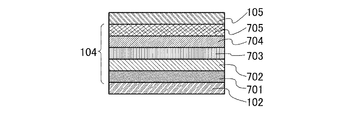
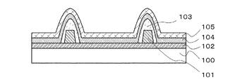
本実施の形態で説明する発光装置は、基板100上に補助配線101を有し、基板100と補助配線101を覆う第1の電極102を有する。また、第1の電極102上で補助配線101によって生じる段差を覆う絶縁物103を有する。さらに、第1の電極102と絶縁物103を覆うEL層104を有し、EL層104上に第2の電極105を有する。なお、図1(A)は基板100、補助配線101、第1の電極102および絶縁物103を有する構成の発光装置の上面図、図1(B)は図1(A)のa−b間の断面図、図1(C)は基板100、補助配線101、第1の電極102、絶縁物103、EL層104および第2の電極105を有する構成の発光装置の断面図を示している。
The light-emitting device described in this embodiment includes an
基板100としては、透光性を有する基板を用いる。具体的には、ガラス、石英、プラスチック、ポリエステル、ポリカーボネートまたはアクリル樹脂のような透光性を有する材料を用いることができる。また、基板100は可撓性を有していてもよい。可撓性基板とは、折り曲げることができる(フレキシブル)基板のことであり、例えば、ポリカーボネート、ポリアリレート、ポリエーテルスルフォンからなるプラスチック基板等が挙げられる。また、フィルム(ポリプロピレン、ポリエステル、ビニル、ポリフッ化ビニル、ポリ塩化ビニルなどからなる)、無機蒸着フィルムを用いることもできる。なお、支持体として機能するものであれば、これら以外のものでもよい。また、基板の形状は正方形、長方形、多角形、円形またはディスク形状(円盤形状)などを用いることができる。
As the
基板100上に補助配線101が形成される。補助配線101としては、抵抗率の低い材料を用いることが好ましく、具体的にはアルミニウム、銅、銀等の材料を用いることができる。また、アルミニウム合金(Al−Nd、Al−Ti等)や複数の金属の積層(Ti\Al\Ti、Al−Ti\Ti等)を用いると低抵抗と高温処理に対する耐性の両立が可能である。その他、用途によってはチタン、タングステン、タンタル、モリブデンなど比較的高抵抗な材料を補助配線として用いてもよい。補助配線の厚さ、幅、および設置間隔は第1の電極による電圧降下に起因する、EL発光輝度のばらつきを考慮して決定される。具体的には、電圧降下によるEL発光輝度のばらつきを10%以内に抑えるように設置することが望ましい。
An
続いて、基板100および補助配線101上に第1の電極102が形成される。このとき、第1の電極102は隣り合う補助配線間で分断されることなく連続して形成されている。第1の電極102はEL層からの光を透過することが可能な材料、厚さで形成する。
Subsequently, the
なお、本発明では、補助配線101を設けているため、第1の電極102が高抵抗であっても使用可能である。つまり、高抵抗な部類に属する導電性高分子を第1の電極102として用いることができる。導電性高分子としては、いわゆるπ電子共役系導電性高分子を用いることができる。例えばπ電子共役系導電性高分子として、ポリアニリン及びまたはその誘導体、ポリピロール及びまたはその誘導体、ポリチオフェン及びまたはその誘導体、またはアニリン、ピロール及びチオフェンの2種以上からなる共重合体またはその誘導体などがあげられる。第1の電極102に導電性高分子を用いることで、スピンコートなど湿式法により簡便に第1の電極102を形成することができ、且つEL層の正孔注入層が不要となることから、生産性の高い発光装置を提供することができる。
In the present invention, since the
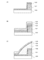
また、本実施の形態の発光装置は、補助配線のパターン形成工程が第1の電極形成の前に行われるため、第1の電極は補助配線のエッチング工程の影響を受けない。そのため、第1の電極102を導電性高分子で形成しても、補助配線のパターン形成工程により導電性高分子がダメージを受けなくて済む。また、第1の電極102を非常に薄くすることができる。具体的には第1の電極102の膜厚を10nm以下にすることができる。第1の電極102を非常に薄くする場合は、あらかじめ補助配線の端部を図3に示すようなテーパー形状にしておくことが望ましい。例えば70度から85度の傾斜を有するテーパー形状にすることで、第1の電極の断線を防止することができる。第1の電極102を薄くすることによって第1の電極による光の損失を低減することができるため、消費電力の低い発光装置を提供することができる。
In the light-emitting device of this embodiment mode, since the auxiliary wiring pattern formation step is performed before the first electrode formation, the first electrode is not affected by the auxiliary wiring etching step. Therefore, even if the
次に、第1の電極102上に、補助配線101によって生じる段差を覆うように絶縁物103が形成される。絶縁物103としては、無機材料(酸化シリコン、窒化シリコン、酸化窒化シリコン等)、感光性又は非感光性の有機材料(ポリイミド、アクリル、ポリアミド、ポリイミドアミド、レジスト又はベンゾシクロブテン)、シロキサン及びそれらの積層構造を用いることができる。有機材料として、ポジ型感光性有機樹脂又はネガ型感光性有機樹脂を用いることができる。
Next, an
絶縁物103の作製方法は、スパッタリング法、プラズマCVD法、真空蒸着法など乾式の成膜方法とスピンコート法、インクジェット法、スプレー塗布法、スクリーン印刷法などの湿式の成膜法があり、材料に応じて作製方法を選択できる。
As a manufacturing method of the
なお、絶縁物103は補助配線101によって生じる段差の上面と側面を覆ってもよい。補助配線によって生じる段差の上面と側面を絶縁物で覆った例を図2(A)乃至図2(C)に示す。
Note that the
図2(A)は基板100、補助配線101、第1の電極102および絶縁物103を有する構成の上面図、図2(B)は図2(A)のa−b間の断面図、図2(C)は基板100、補助配線101、第1の電極102、絶縁物103、EL層104および第2の電極105を有する構成の断面図を示している。
2A is a top view of a structure including the
このように補助配線101によって生じる段差の上面と側面の両方を絶縁物103により覆うことで、短絡を防ぐことができるほか、補助配線によって遮られてしまうため取り出すことができない、補助配線の上面と第2の電極の間のEL層が発する発光に消費される電力を抑えた発光装置を提供することができる。
Thus, by covering both the upper surface and the side surface of the step generated by the
第1の電極102と絶縁物103上にはEL層104が形成され、EL層104の上に第2の電極105が形成される。ここで、第1の電極とEL層と第2の電極からなるEL素子構造について、図4及び図5を用いて詳細に説明する。
An
第1の電極102が陽極である場合は、酸化インジウム(In2O3)や酸化インジウム酸化スズ合金(In2O3―SnO2;ITO)などをスパッタ法や真空蒸着法などを用いて形成して用いることができる。酸化インジウム酸化亜鉛合金(In2O3―ZnO)を用いても良い。また、酸化亜鉛(ZnO)も適した材料であり、さらに可視光の透過率や導電率を高めるためにガリウム(Ga)を添加した酸化亜鉛(ZnO:Ga)などを用いることができる。これらの導電性金属酸化物膜は、通常スパッタにより成膜されるが、ゾル−ゲル法などを応用して作製しても構わない。この他、金(Au)、白金(Pt)、ニッケル(Ni)、タングステン(W)、クロム(Cr)、モリブデン(Mo)、鉄(Fe)、コバルト(Co)、銅(Cu)、パラジウム(Pd)、チタン(Ti)または金属材料の窒化物(例えば、窒化チタン)等が挙げられる。なお、金属材料を用いる場合、必要に応じて光を透過可能な程度に薄くすることができる。第1の電極102を陰極とする場合には、アルミニウムなど仕事関数の低い材料の極薄膜を用いるか、そのような物質の薄膜と透明導電膜との積層構造を用いることによって作製することができる。
When the
EL層104の積層構造については特に限定されず、電子輸送性の高い物質を含む層または正孔輸送性の高い物質を含む層、電子注入性の高い物質を含む層、正孔注入性の高い物質を含む層、バイポーラ性(電子及び正孔の輸送性の高い物質)の物質を含む層等を適宜組み合わせて構成すればよい。例えば、正孔注入層、正孔輸送層、発光層、電子輸送層、電子注入層等を適宜組み合わせて構成することができる。本実施の形態では、EL層104は、正孔注入層701、正孔輸送層702、発光層703、電子輸送層704、電子注入層705を有する構成について説明する(図4参照)。各層を構成する材料について以下に具体的に示す。
There is no particular limitation on the stacked structure of the
正孔注入層701は、陽極に接して設けられ、正孔注入性の高い物質を含む層である。モリブデン酸化物やバナジウム酸化物、ルテニウム酸化物、タングステン酸化物、マンガン酸化物等を用いることができる。この他、フタロシアニン(略称:H2Pc)や銅フタロシアニン(略称:CuPC)等のフタロシアニン系の化合物、4,4’−ビス[N−(4−ジフェニルアミノフェニル)−N−フェニルアミノ]ビフェニル(略称:DPAB)、N,N’−ビス[4−[ビス(3−メチルフェニル)アミノ]フェニル]−N,N’−ジフェニル−[1,1’−ビフェニル]−4,4’−ジアミン(略称:DNTPD)等の芳香族アミン化合物、或いはポリ(エチレンジオキシチオフェン)/ポリ(スチレンスルホン酸)(PEDOT/PSS)等の高分子等によっても正孔注入層701を形成することができる。
The
また、正孔注入層701として、正孔輸送性の高い物質にアクセプター性物質を含有させた複合材料を用いることができる。なお、正孔輸送性の高い物質にアクセプター性物質を含有させたものを用いることにより、電極の仕事関数に依らず電極を形成する材料を選ぶことができる。つまり、第1の電極102として仕事関数の大きい材料だけでなく、仕事関数の小さい材料を用いることができる。アクセプター性物質としては、7,7,8,8−テトラシアノ−2,3,5,6−テトラフルオロキノジメタン(略称:F4−TCNQ)、クロラニル等を挙げることができる。また、遷移金属酸化物を挙げることができる。また元素周期表における第4族乃至第8族に属する金属の酸化物を挙げることができる。具体的には、酸化バナジウム、酸化ニオブ、酸化タンタル、酸化クロム、酸化モリブデン、酸化タングステン、酸化マンガン、酸化レニウムは電子受容性が高いため好ましい。中でも特に、酸化モリブデンは大気中でも安定であり、吸湿性が低く、扱いやすいため好ましい。
For the hole-injecting
複合材料に用いる正孔輸送性の高い物質としては、芳香族アミン化合物、カルバゾール誘導体、芳香族炭化水素、高分子化合物(オリゴマー、デンドリマー、ポリマー等)など、種々の化合物を用いることができる。なお、複合材料に用いる有機化合物としては、正孔輸送性の高い有機化合物であることが好ましい。具体的には、10−6cm2/Vs以上の正孔移動度を有する物質であることが好ましい。但し、電子よりも正孔の輸送性の高い物質であれば、これら以外のものを用いてもよい。以下では、複合材料に用いることのできる有機化合物を具体的に列挙する。 As the substance having a high hole-transport property used for the composite material, various compounds such as an aromatic amine compound, a carbazole derivative, an aromatic hydrocarbon, and a high molecular compound (oligomer, dendrimer, polymer, and the like) can be used. Note that the organic compound used for the composite material is preferably an organic compound having a high hole-transport property. Specifically, a substance having a hole mobility of 10 −6 cm 2 / Vs or higher is preferable. Note that other than these substances, any substance that has a property of transporting more holes than electrons may be used. Below, the organic compound which can be used for a composite material is listed concretely.
例えば、芳香族アミン化合物としては、N,N’−ジ(p−トリル)−N,N’−ジフェニル−p−フェニレンジアミン(略称:DTDPPA)、4,4’−ビス[N−(4−ジフェニルアミノフェニル)−N−フェニルアミノ]ビフェニル(略称:DPAB)、N,N’−ビス[4−[ビス(3−メチルフェニル)アミノ]フェニル]−N,N’−ジフェニル−[1,1’−ビフェニル]−4,4’−ジアミン(略称:DNTPD)、1,3,5−トリス[N−(4−ジフェニルアミノフェニル)−N−フェニルアミノ]ベンゼン(略称:DPA3B)等を挙げることができる。 For example, as an aromatic amine compound, N, N′-di (p-tolyl) -N, N′-diphenyl-p-phenylenediamine (abbreviation: DTDPPA), 4,4′-bis [N- (4- Diphenylaminophenyl) -N-phenylamino] biphenyl (abbreviation: DPAB), N, N′-bis [4- [bis (3-methylphenyl) amino] phenyl] -N, N′-diphenyl- [1,1 '-Biphenyl] -4,4'-diamine (abbreviation: DNTPD), 1,3,5-tris [N- (4-diphenylaminophenyl) -N-phenylamino] benzene (abbreviation: DPA3B), etc. Can do.
複合材料に用いることのできるカルバゾール誘導体としては、具体的には、3−[N−(9−フェニルカルバゾール−3−イル)−N−フェニルアミノ]−9−フェニルカルバゾール(略称:PCzPCA1)、3,6−ビス[N−(9−フェニルカルバゾール−3−イル)−N−フェニルアミノ]−9−フェニルカルバゾール(略称:PCzPCA2)、3−[N−(1−ナフチル)−N−(9−フェニルカルバゾール−3−イル)アミノ]−9−フェニルカルバゾール(略称:PCzPCN1)等を挙げることができる。 Specific examples of the carbazole derivative that can be used for the composite material include 3- [N- (9-phenylcarbazol-3-yl) -N-phenylamino] -9-phenylcarbazole (abbreviation: PCzPCA1), 3 , 6-Bis [N- (9-phenylcarbazol-3-yl) -N-phenylamino] -9-phenylcarbazole (abbreviation: PCzPCA2), 3- [N- (1-naphthyl) -N- (9- Phenylcarbazol-3-yl) amino] -9-phenylcarbazole (abbreviation: PCzPCN1) and the like.
また、複合材料に用いることのできるカルバゾール誘導体としては、他に、4,4’−ジ(N−カルバゾリル)ビフェニル(略称:CBP)、1,3,5−トリス[4−(N−カルバゾリル)フェニル]ベンゼン(略称:TCPB)、9−[4−(10−フェニル−9−アントリル)フェニル]−9H−カルバゾール(略称:CzPA)、1,4−ビス[4−(N−カルバゾリル)フェニル]−2,3,5,6−テトラフェニルベンゼン等を用いることができる。 As other carbazole derivatives that can be used for the composite material, 4,4′-di (N-carbazolyl) biphenyl (abbreviation: CBP), 1,3,5-tris [4- (N-carbazolyl) Phenyl] benzene (abbreviation: TCPB), 9- [4- (10-phenyl-9-anthryl) phenyl] -9H-carbazole (abbreviation: CzPA), 1,4-bis [4- (N-carbazolyl) phenyl] -2,3,5,6-tetraphenylbenzene and the like can be used.
また、複合材料に用いることのできる芳香族炭化水素としては、例えば、2−tert−ブチル−9,10−ジ(2−ナフチル)アントラセン(略称:t−BuDNA)、2−tert−ブチル−9,10−ジ(1−ナフチル)アントラセン、9,10−ビス(3,5−ジフェニルフェニル)アントラセン(略称:DPPA)、2−tert−ブチル−9,10−ビス(4−フェニルフェニル)アントラセン(略称:t−BuDBA)、9,10−ジ(2−ナフチル)アントラセン(略称:DNA)、9,10−ジフェニルアントラセン(略称:DPAnth)、2−tert−ブチルアントラセン(略称:t−BuAnth)、9,10−ビス(4−メチル−1−ナフチル)アントラセン(略称:DMNA)、2−tert−ブチル−9,10−ビス[2−(1−ナフチル)フェニル]アントラセン、9,10−ビス[2−(1−ナフチル)フェニル]アントラセン、2,3,6,7−テトラメチル−9,10−ジ(1−ナフチル)アントラセン、2,3,6,7−テトラメチル−9,10−ジ(2−ナフチル)アントラセン、9,9’−ビアントリル、10,10’−ジフェニル−9,9’−ビアントリル、10,10’−ビス(2−フェニルフェニル)−9,9’−ビアントリル、10,10’−ビス[(2,3,4,5,6−ペンタフェニル)フェニル]−9,9’−ビアントリル、アントラセン、テトラセン、ルブレン、ペリレン、2,5,8,11−テトラ(tert−ブチル)ペリレン等が挙げられる。また、この他、ペンタセン、コロネン等も用いることができる。このように、1×10−6cm2/Vs以上の正孔移動度を有し、炭素数14〜42である芳香族炭化水素を用いることがより好ましい。 Examples of aromatic hydrocarbons that can be used for the composite material include 2-tert-butyl-9,10-di (2-naphthyl) anthracene (abbreviation: t-BuDNA), 2-tert-butyl-9. , 10-di (1-naphthyl) anthracene, 9,10-bis (3,5-diphenylphenyl) anthracene (abbreviation: DPPA), 2-tert-butyl-9,10-bis (4-phenylphenyl) anthracene ( Abbreviations: t-BuDBA), 9,10-di (2-naphthyl) anthracene (abbreviation: DNA), 9,10-diphenylanthracene (abbreviation: DPAnth), 2-tert-butylanthracene (abbreviation: t-BuAnth), 9,10-bis (4-methyl-1-naphthyl) anthracene (abbreviation: DMNA), 2-tert-butyl-9, 0-bis [2- (1-naphthyl) phenyl] anthracene, 9,10-bis [2- (1-naphthyl) phenyl] anthracene, 2,3,6,7-tetramethyl-9,10-di (1 -Naphthyl) anthracene, 2,3,6,7-tetramethyl-9,10-di (2-naphthyl) anthracene, 9,9'-bianthryl, 10,10'-diphenyl-9,9'-bianthryl, 10 , 10′-bis (2-phenylphenyl) -9,9′-bianthryl, 10,10′-bis [(2,3,4,5,6-pentaphenyl) phenyl] -9,9′-bianthryl, Anthracene, tetracene, rubrene, perylene, 2,5,8,11-tetra (tert-butyl) perylene and the like can be mentioned. In addition, pentacene, coronene, and the like can also be used. Thus, it is more preferable to use an aromatic hydrocarbon having a hole mobility of 1 × 10 −6 cm 2 / Vs or more and having 14 to 42 carbon atoms.
なお、複合材料に用いることのできる芳香族炭化水素は、ビニル骨格を有していてもよい。ビニル基を有している芳香族炭化水素としては、例えば、4,4’−ビス(2,2−ジフェニルビニル)ビフェニル(略称:DPVBi)、9,10−ビス[4−(2,2−ジフェニルビニル)フェニル]アントラセン(略称:DPVPA)等が挙げられる。 Note that the aromatic hydrocarbon that can be used for the composite material may have a vinyl skeleton. As the aromatic hydrocarbon having a vinyl group, for example, 4,4′-bis (2,2-diphenylvinyl) biphenyl (abbreviation: DPVBi), 9,10-bis [4- (2,2- Diphenylvinyl) phenyl] anthracene (abbreviation: DPVPA) and the like.
また、ポリ(N−ビニルカルバゾール)(略称:PVK)やポリ(4−ビニルトリフェニルアミン)(略称:PVTPA)、ポリ[N−(4−{N’−[4−(4−ジフェニルアミノ)フェニル]フェニル−N’−フェニルアミノ}フェニル)メタクリルアミド](略称:PTPDMA)ポリ[N,N’−ビス(4−ブチルフェニル)−N,N’−ビス(フェニル)ベンジジン](略称:Poly−TPD)等の高分子化合物を用いることもできる。 In addition, poly (N-vinylcarbazole) (abbreviation: PVK), poly (4-vinyltriphenylamine) (abbreviation: PVTPA), poly [N- (4- {N ′-[4- (4-diphenylamino)] Phenyl] phenyl-N′-phenylamino} phenyl) methacrylamide] (abbreviation: PTPDMA) poly [N, N′-bis (4-butylphenyl) -N, N′-bis (phenyl) benzidine] (abbreviation: Poly High molecular compounds such as -TPD) can also be used.
正孔輸送層702は、正孔輸送性の高い物質を含む層である。正孔輸送性の高い物質としては、例えば、4,4’−ビス[N−(1−ナフチル)−N−フェニルアミノ]ビフェニル(略称:NPB)やN,N’−ビス(3−メチルフェニル)−N,N’−ジフェニル−[1,1’−ビフェニル]−4,4’−ジアミン(略称:TPD)、4,4’,4’’−トリス(N,N−ジフェニルアミノ)トリフェニルアミン(略称:TDATA)、4,4’,4’’−トリス[N−(3−メチルフェニル)−N−フェニルアミノ]トリフェニルアミン(略称:MTDATA)、4,4’−ビス[N−(スピロ−9,9’−ビフルオレン−2−イル)−N―フェニルアミノ]ビフェニル(略称:BSPB)などの芳香族アミン化合物等を用いることができる。ここに述べた物質は、主に10−6cm2/Vs以上の正孔移動度を有する物質である。但し、電子よりも正孔の輸送性の高い物質であれば、これら以外のものを用いてもよい。なお、正孔輸送性の高い物質を含む層は、単層のものだけでなく、上記物質からなる層が二層以上積層したものとしてもよい。
The hole-
また、正孔輸送層702として、ポリ(N−ビニルカルバゾール)(略称:PVK)やポリ(4−ビニルトリフェニルアミン)(略称:PVTPA)等の高分子化合物を用いることもできる。
For the hole-
発光層703は、発光性の物質を含む層である。発光層703の種類としては、発光中心物質を主成分とするいわゆる単膜の発光層であっても、ホスト材料中に発光中心材料を分散するいわゆるホスト−ゲスト型の発光層であってもどちらでも構わない。
The
用いられる発光中心材料に制限は無く、公知の蛍光又は燐光を発する材料を用いることができる。蛍光発光性材料としては、例えばN,N’−ビス[4−(9H−カルバゾール−9−イル)フェニル]−N,N’−ジフェニルスチルベン−4,4’−ジアミン(略称:YGA2S)、4−(9H−カルバゾール−9−イル)−4’−(10−フェニル−9−アントリル)トリフェニルアミン(略称:YGAPA)、等の他、発光波長が450nm以上の4−(9H−カルバゾール−9−イル)−4’−(9,10−ジフェニル−2−アントリル)トリフェニルアミン(略称:2YGAPPA)、N,9−ジフェニル−N−[4−(10−フェニル−9−アントリル)フェニル]−9H−カルバゾール−3−アミン(略称:PCAPA)、ペリレン、2,5,8,11−テトラ−tert−ブチルペリレン(略称:TBP)、4−(10−フェニル−9−アントリル)−4’−(9−フェニル−9H−カルバゾール−3−イル)トリフェニルアミン(略称:PCBAPA)、N,N’’−(2−tert−ブチルアントラセン−9,10−ジイルジ−4,1−フェニレン)ビス[N,N’,N’−トリフェニル−1,4−フェニレンジアミン](略称:DPABPA)、N,9−ジフェニル−N−[4−(9,10−ジフェニル−2−アントリル)フェニル]−9H−カルバゾール−3−アミン(略称:2PCAPPA)、N−[4−(9,10−ジフェニル−2−アントリル)フェニル]−N,N’,N’−トリフェニル−1,4−フェニレンジアミン(略称:2DPAPPA)、N,N,N’,N’,N’’,N’’,N’’’,N’’’−オクタフェニルジベンゾ[g,p]クリセン−2,7,10,15−テトラアミン(略称:DBC1)、クマリン30、N−(9,10−ジフェニル−2−アントリル)−N,9−ジフェニル−9H−カルバゾール−3−アミン(略称:2PCAPA)、N−[9,10−ビス(1,1’−ビフェニル−2−イル)−2−アントリル]−N,9−ジフェニル−9H−カルバゾール−3−アミン(略称:2PCABPhA)、N−(9,10−ジフェニル−2−アントリル)−N,N’,N’−トリフェニル−1,4−フェニレンジアミン(略称:2DPAPA)、N−[9,10−ビス(1,1’−ビフェニル−2−イル)−2−アントリル]−N,N’,N’−トリフェニル−1,4−フェニレンジアミン(略称:2DPABPhA)、9,10−ビス(1,1’−ビフェニル−2−イル)−N−[4−(9H−カルバゾール−9−イル)フェニル]−N−フェニルアントラセン−2−アミン(略称:2YGABPhA)、N,N,9−トリフェニルアントラセン−9−アミン(略称:DPhAPhA)、クマリン545T、N,N’−ジフェニルキナクリドン、(略称:DPQd)、ルブレン、5,12−ビス(1,1’−ビフェニル−4−イル)−6,11−ジフェニルテトラセン(略称:BPT)、2−(2−{2−[4−(ジメチルアミノ)フェニル]エテニル}−6−メチル−4H−ピラン−4−イリデン)プロパンジニトリル(略称:DCM1)、2−{2−メチル−6−[2−(2,3,6,7−テトラヒドロ−1H,5H−ベンゾ[ij]キノリジン−9−イル)エテニル]−4H−ピラン−4−イリデン}プロパンジニトリル(略称:DCM2)、N,N,N’,N’−テトラキス(4−メチルフェニル)テトラセン−5,11−ジアミン(略称:p−mPhTD)、7,14−ジフェニル−N,N,N’,N’−テトラキス(4−メチルフェニル)アセナフト[1,2−a]フルオランテン−3,10−ジアミン(略称:p−mPhAFD)、2−{2−イソプロピル−6−[2−(1,1,7,7−テトラメチル−2,3,6,7−テトラヒドロ−1H,5H−ベンゾ[ij]キノリジン−9−イル)エテニル]−4H−ピラン−4−イリデン}プロパンジニトリル(略称:DCJTI)、2−{2−tert−ブチル−6−[2−(1,1,7,7−テトラメチル−2,3,6,7−テトラヒドロ−1H,5H−ベンゾ[ij]キノリジン−9−イル)エテニル]−4H−ピラン−4−イリデン}プロパンジニトリル(略称:DCJTB)、2−(2,6−ビス{2−[4−(ジメチルアミノ)フェニル]エテニル}−4H−ピラン−4−イリデン)プロパンジニトリル(略称:BisDCM)、2−{2,6−ビス[2−(8−メトキシ−1,1,7,7−テトラメチル−2,3,6,7−テトラヒドロ−1H,5H−ベンゾ[ij]キノリジン−9−イル)エテニル]−4H−ピラン−4−イリデン}プロパンジニトリル(略称:BisDCJTM)などが挙げられる。燐光発光性材料としては、例えば、ビス[2−(4’,6’−ジフルオロフェニル)ピリジナト−N,C2’]イリジウム(III)テトラキス(1−ピラゾリル)ボラート(略称:FIr6)、の他、発光波長が470nm〜500nmの範囲にある、ビス[2−(4’,6’−ジフルオロフェニル)ピリジナト−N,C2’]イリジウム(III)ピコリナート(略称:FIrpic)、ビス[2−(3’,5’−ビストリフルオロメチルフェニル)ピリジナト−N,C2’]イリジウム(III)ピコリナート(略称:Ir(CF3ppy)2(pic))、ビス[2−(4’,6’−ジフルオロフェニル)ピリジナト−N,C2’]イリジウム(III)アセチルアセトナート(略称:FIracac)、発光波長が500nm(緑色発光)以上のトリス(2−フェニルピリジナト)イリジウム(III)(略称:Ir(ppy)3)、ビス(2−フェニルピリジナト)イリジウム(III)アセチルアセトナート(略称:Ir(ppy)2(acac))、トリス(アセチルアセトナト)(モノフェナントロリン)テルビウム(III)(略称:Tb(acac)3(Phen))、ビス(ベンゾ[h]キノリナト)イリジウム(III)アセチルアセトナート(略称:Ir(bzq)2(acac))、ビス(2,4−ジフェニル−1,3−オキサゾラト−N,C2’)イリジウム(III)アセチルアセトナート(略称:Ir(dpo)2(acac))、ビス[2−(4’−パーフルオロフェニルフェニル)ピリジナト]イリジウム(III)アセチルアセトナート(略称:Ir(p−PF−ph)2(acac))、ビス(2−フェニルベンゾチアゾラト−N,C2’)イリジウム(III)アセチルアセトナート(略称:Ir(bt)2(acac))、ビス[2−(2’−ベンゾ[4,5−α]チエニル)ピリジナト−N,C3’]イリジウム(III)アセチルアセトナート(略称:Ir(btp)2(acac))、ビス(1−フェニルイソキノリナト−N,C2’)イリジウム(III)アセチルアセトナート(略称:Ir(piq)2(acac))、(アセチルアセトナト)ビス[2,3−ビス(4−フルオロフェニル)キノキサリナト]イリジウム(III)(略称:Ir(Fdpq)2(acac))、(アセチルアセトナト)ビス(2,3,5−トリフェニルピラジナト)イリジウム(III)(略称:Ir(tppr)2(acac))、2,3,7,8,12,13,17,18−オクタエチル−21H,23H−ポルフィリン白金(II)(略称:PtOEP)、トリス(1,3−ジフェニル−1,3−プロパンジオナト)(モノフェナントロリン)ユーロピウム(III)(略称:Eu(DBM)3(Phen))、トリス[1−(2−テノイル)−3,3,3−トリフルオロアセトナト](モノフェナントロリン)ユーロピウム(III)(略称:Eu(TTA)3(Phen))等が挙げられる。以上のような材料又は他の公知の材料の中から、各々の発光素子における発光色を考慮し選択すれば良い。 There is no restriction | limiting in the luminescent center material used, The material which emits well-known fluorescence or phosphorescence can be used. As a fluorescent material, for example, N, N′-bis [4- (9H-carbazol-9-yl) phenyl] -N, N′-diphenylstilbene-4,4′-diamine (abbreviation: YGA2S), 4 -(9H-carbazol-9-yl) -4 '-(10-phenyl-9-anthryl) triphenylamine (abbreviation: YGAPA), etc., and 4- (9H-carbazole-9 having an emission wavelength of 450 nm or more -Yl) -4 '-(9,10-diphenyl-2-anthryl) triphenylamine (abbreviation: 2YGAPPA), N, 9-diphenyl-N- [4- (10-phenyl-9-anthryl) phenyl]- 9H-carbazol-3-amine (abbreviation: PCAPA), perylene, 2,5,8,11-tetra-tert-butylperylene (abbreviation: TBP), 4- (10-phenyl) 9-anthryl) -4 ′-(9-phenyl-9H-carbazol-3-yl) triphenylamine (abbreviation: PCBAPA), N, N ″-(2-tert-butylanthracene-9,10-diyldi- 4,1-phenylene) bis [N, N ′, N′-triphenyl-1,4-phenylenediamine] (abbreviation: DPABPA), N, 9-diphenyl-N- [4- (9,10-diphenyl-) 2-anthryl) phenyl] -9H-carbazol-3-amine (abbreviation: 2PCAPPA), N- [4- (9,10-diphenyl-2-anthryl) phenyl] -N, N ′, N′-triphenyl- 1,4-phenylenediamine (abbreviation: 2DPAPPA), N, N, N ′, N ′, N ″, N ″, N ′ ″, N ′ ″-octaphenyldibenzo [g, p] chrysene- 2,7,10,15-te Laamine (abbreviation: DBC1), Coumarin 30, N- (9,10-diphenyl-2-anthryl) -N, 9-diphenyl-9H-carbazol-3-amine (abbreviation: 2PCAPA), N- [9,10- Bis (1,1′-biphenyl-2-yl) -2-anthryl] -N, 9-diphenyl-9H-carbazol-3-amine (abbreviation: 2PCABPhA), N- (9,10-diphenyl-2-anthryl) ) -N, N ′, N′-triphenyl-1,4-phenylenediamine (abbreviation: 2DPAPA), N- [9,10-bis (1,1′-biphenyl-2-yl) -2-anthryl] -N, N ', N'-triphenyl-1,4-phenylenediamine (abbreviation: 2DPABPhA), 9,10-bis (1,1'-biphenyl-2-yl) -N- [4- (9H- Carbazo Ru-9-yl) phenyl] -N-phenylanthracen-2-amine (abbreviation: 2YGABPhA), N, N, 9-triphenylanthracen-9-amine (abbreviation: DPhAPhA), coumarin 545T, N, N'- Diphenylquinacridone, (abbreviation: DPQd), rubrene, 5,12-bis (1,1′-biphenyl-4-yl) -6,11-diphenyltetracene (abbreviation: BPT), 2- (2- {2- [ 4- (dimethylamino) phenyl] ethenyl} -6-methyl-4H-pyran-4-ylidene) propanedinitrile (abbreviation: DCM1), 2- {2-methyl-6- [2- (2,3,6) , 7-Tetrahydro-1H, 5H-benzo [ij] quinolizin-9-yl) ethenyl] -4H-pyran-4-ylidene} propanedinitrile (abbreviation: DCM2) N, N, N ′, N′-tetrakis (4-methylphenyl) tetracene-5,11-diamine (abbreviation: p-mPhTD), 7,14-diphenyl-N, N, N ′, N′-tetrakis ( 4-methylphenyl) acenaphtho [1,2-a] fluoranthene-3,10-diamine (abbreviation: p-mPhAFD), 2- {2-isopropyl-6- [2- (1,1,7,7-tetra Methyl-2,3,6,7-tetrahydro-1H, 5H-benzo [ij] quinolizin-9-yl) ethenyl] -4H-pyran-4-ylidene} propanedinitrile (abbreviation: DCJTI), 2- {2 -Tert-butyl-6- [2- (1,1,7,7-tetramethyl-2,3,6,7-tetrahydro-1H, 5H-benzo [ij] quinolizin-9-yl) ethenyl] -4H -Pyran-4- Ridene} propanedinitrile (abbreviation: DCJTB), 2- (2,6-bis {2- [4- (dimethylamino) phenyl] ethenyl} -4H-pyran-4-ylidene) propanedinitrile (abbreviation: BisDCM) 2- {2,6-bis [2- (8-methoxy-1,1,7,7-tetramethyl-2,3,6,7-tetrahydro-1H, 5H-benzo [ij] quinolidine-9- Yl) ethenyl] -4H-pyran-4-ylidene} propanedinitrile (abbreviation: BisDCJTM). Examples of the phosphorescent material include bis [2- (4 ′, 6′-difluorophenyl) pyridinato-N, C 2 ′ ] iridium (III) tetrakis (1-pyrazolyl) borate (abbreviation: FIr6), and the like. , Bis [2- (4 ′, 6′-difluorophenyl) pyridinato-N, C 2 ′ ] iridium (III) picolinate (abbreviation: FIrpic), bis [2- ( 3 ′, 5′-bistrifluoromethylphenyl) pyridinato-N, C 2 ′ ] iridium (III) picolinate (abbreviation: Ir (CF 3 ppy) 2 (pic)), bis [2- (4 ′, 6′- difluorophenyl) pyridinato -N, C 2 '] iridium (III) acetylacetonate (abbreviation: FIracac), emission wavelength 500 nm (green emission) Tris upper (2-phenylpyridinato) iridium (III) (abbreviation: Ir (ppy) 3), bis (2-phenylpyridinato) iridium (III) acetylacetonate (abbreviation: Ir (ppy) 2 ( acac)), tris (acetylacetonato) (monophenanthroline) terbium (III) (abbreviation: Tb (acac) 3 (Phen)), bis (benzo [h] quinolinato) iridium (III) acetylacetonate (abbreviation: Ir (Bzq) 2 (acac)), bis (2,4-diphenyl-1,3-oxazolate-N, C 2 ′ ) iridium (III) acetylacetonate (abbreviation: Ir (dpo) 2 (acac)), bis [2- (4′-perfluorophenylphenyl) pyridinato] iridium (III) acetylacetonate ( Abbreviations: Ir (p-PF-ph) 2 (acac)), bis (2-phenylbenzothiazolate-N, C 2 ′ ) iridium (III) acetylacetonate (abbreviation: Ir (bt) 2 (acac) ), Bis [2- (2′-benzo [4,5-α] thienyl) pyridinato-N, C 3 ′ ] iridium (III) acetylacetonate (abbreviation: Ir (btp) 2 (acac)), bis ( 1-phenylisoquinolinato-N, C 2 ′ ) iridium (III) acetylacetonate (abbreviation: Ir (piq) 2 (acac)), (acetylacetonato) bis [2,3-bis (4-fluorophenyl) ) Quinoxalinato] iridium (III) (abbreviation: Ir (Fdpq) 2 (acac)), (acetylacetonato) bis (2,3,5-triphenylpyrazinato) irid Um (III) (abbreviation: Ir (tppr) 2 (acac)), 2,3,7,8,12,13,17,18-octaethyl-21H, 23H-porphyrin platinum (II) (abbreviation: PtOEP), Tris (1,3-diphenyl-1,3-propanedionate) (monophenanthroline) europium (III) (abbreviation: Eu (DBM) 3 (Phen)), tris [1- (2-thenoyl) -3,3 , 3-trifluoroacetonato] (monophenanthroline) europium (III) (abbreviation: Eu (TTA) 3 (Phen)) and the like. What is necessary is just to select in consideration of the luminescent color in each light emitting element from the above materials or other known materials.
ホスト材料を用いる場合は、例えばトリス(8−キノリノラト)アルミニウム(III)(略称:Alq)、トリス(4−メチル−8−キノリノラト)アルミニウム(III)(略称:Almq3)、ビス(10−ヒドロキシベンゾ[h]キノリナト)ベリリウム(II)(略称:BeBq2)、ビス(2−メチル−8−キノリノラト)(4−フェニルフェノラト)アルミニウム(III)(略称:BAlq)、ビス(8−キノリノラト)亜鉛(II)(略称:Znq)、ビス[2−(2−ベンゾオキサゾリル)フェノラト]亜鉛(II)(略称:ZnPBO)、ビス[2−(2−ベンゾチアゾリル)フェノラト]亜鉛(II)(略称:ZnBTZ)などの金属錯体、2−(4−ビフェニリル)−5−(4−tert−ブチルフェニル)−1,3,4−オキサジアゾール(略称:PBD)、1,3−ビス[5−(p−tert−ブチルフェニル)−1,3,4−オキサジアゾール−2−イル]ベンゼン(略称:OXD−7)、3−(4−ビフェニリル)−4−フェニル−5−(4−tert−ブチルフェニル)−1,2,4−トリアゾール(略称:TAZ)、2,2’,2’’−(1,3,5−ベンゼントリイル)トリス(1−フェニル−1H−ベンゾイミダゾール)(略称:TPBI)、バソフェナントロリン(略称:BPhen)、バソキュプロイン(略称:BCP)、9−[4−(5−フェニル−1,3,4−オキサジアゾール−2−イル)フェニル]−9H−カルバゾール(略称:CO11)などの複素環化合物、NPB(またはα−NPD)、TPD、BSPBなどの芳香族アミン化合物が挙げられる。また、アントラセン誘導体、フェナントレン誘導体、ピレン誘導体、クリセン誘導体、ジベンゾ[g,p]クリセン誘導体等の縮合多環芳香族化合物が挙げられ、具体的には、9,10−ジフェニルアントラセン(略称:DPAnth)、N,N−ジフェニル−9−[4−(10−フェニル−9−アントリル)フェニル]−9H−カルバゾール−3−アミン(略称:CzA1PA)、4−(10−フェニル−9−アントリル)トリフェニルアミン(略称:DPhPA)、4−(9H−カルバゾール−9−イル)−4’−(10−フェニル−9−アントリル)トリフェニルアミン(略称:YGAPA)、N,9−ジフェニル−N−[4−(10−フェニル−9−アントリル)フェニル]−9H−カルバゾール−3−アミン(略称:PCAPA)、N,9−ジフェニル−N−{4−[4−(10−フェニル−9−アントリル)フェニル]フェニル}−9H−カルバゾール−3−アミン(略称:PCAPBA)、N,9−ジフェニル−N−(9,10−ジフェニル−2−アントリル)−9H−カルバゾール−3−アミン(略称:2PCAPA)、6,12−ジメトキシ−5,11−ジフェニルクリセン、N,N,N’,N’,N’’,N’’,N’’’,N’’’−オクタフェニルジベンゾ[g,p]クリセン−2,7,10,15−テトラアミン(略称:DBC1)、9−[4−(10−フェニル−9−アントリル)フェニル]−9H−カルバゾール(略称:CzPA)、3,6−ジフェニル−9−[4−(10−フェニル−9−アントリル)フェニル]−9H−カルバゾール(略称:DPCzPA)、9,10−ビス(3,5−ジフェニルフェニル)アントラセン(略称:DPPA)、9,10−ジ(2−ナフチル)アントラセン(略称:DNA)、2−tert−ブチル−9,10−ジ(2−ナフチル)アントラセン(略称:t−BuDNA)、9,9’−ビアントリル(略称:BANT)、9,9’−(スチルベン−3,3’−ジイル)ジフェナントレン(略称:DPNS)、9,9’−(スチルベン−4,4’−ジイル)ジフェナントレン(略称:DPNS2)、3,3’,3’’−(ベンゼン−1,3,5−トリイル)トリピレン(略称:TPB3)などを挙げることができる。これら及び公知の物質の中から、各々が分散する発光中心物質のエネルギーギャップ(燐光発光の場合は三重項エネルギー)より大きなエネルギーギャップ(三重項エネルギー)を有する物質を有し、且つ各々の層が有すべき輸送性に合致した輸送性を示す物質を選択すればよい。 In the case of using a host material, for example, tris (8-quinolinolato) aluminum (III) (abbreviation: Alq), tris (4-methyl-8-quinolinolato) aluminum (III) (abbreviation: Almq 3 ), bis (10-hydroxy) Benzo [h] quinolinato) beryllium (II) (abbreviation: BeBq 2 ), bis (2-methyl-8-quinolinolato) (4-phenylphenolato) aluminum (III) (abbreviation: BAlq), bis (8-quinolinolato) Zinc (II) (abbreviation: Znq), bis [2- (2-benzoxazolyl) phenolato] zinc (II) (abbreviation: ZnPBO), bis [2- (2-benzothiazolyl) phenolato] zinc (II) ( Abbreviations: ZnBTZ) and other metal complexes, 2- (4-biphenylyl) -5- (4-tert-butylphenyl)- 1,3,4-oxadiazole (abbreviation: PBD), 1,3-bis [5- (p-tert-butylphenyl) -1,3,4-oxadiazol-2-yl] benzene (abbreviation: OXD-7), 3- (4-biphenylyl) -4-phenyl-5- (4-tert-butylphenyl) -1,2,4-triazole (abbreviation: TAZ), 2,2 ′, 2 ″- (1,3,5-benzenetriyl) tris (1-phenyl-1H-benzimidazole) (abbreviation: TPBI), bathophenanthroline (abbreviation: BPhen), bathocuproin (abbreviation: BCP), 9- [4- (5 -Phenyl-1,3,4-oxadiazol-2-yl) phenyl] -9H-carbazole (abbreviation: CO11) and other heterocyclic compounds, NPB (or α-NPD), TPD, BSPB and other fragrances Amine compounds. In addition, condensed polycyclic aromatic compounds such as anthracene derivatives, phenanthrene derivatives, pyrene derivatives, chrysene derivatives, and dibenzo [g, p] chrysene derivatives can be given. Specifically, 9,10-diphenylanthracene (abbreviation: DPAnth) N, N-diphenyl-9- [4- (10-phenyl-9-anthryl) phenyl] -9H-carbazol-3-amine (abbreviation: CzA1PA), 4- (10-phenyl-9-anthryl) triphenyl Amine (abbreviation: DPhPA), 4- (9H-carbazol-9-yl) -4 ′-(10-phenyl-9-anthryl) triphenylamine (abbreviation: YGAPA), N, 9-diphenyl-N- [4 -(10-phenyl-9-anthryl) phenyl] -9H-carbazol-3-amine (abbreviation: PCAPA), N, 9-diphenyl-N- {4- [4- (10-phenyl-9-anthryl) phenyl] phenyl} -9H-carbazol-3-amine (abbreviation: PCAPBA), N, 9-diphenyl-N- ( 9,10-diphenyl-2-anthryl) -9H-carbazol-3-amine (abbreviation: 2PCAPA), 6,12-dimethoxy-5,11-diphenylchrysene, N, N, N ′, N ′, N ″ , N ″, N ′ ″, N ′ ″-octaphenyldibenzo [g, p] chrysene-2,7,10,15-tetraamine (abbreviation: DBC1), 9- [4- (10-phenyl- 9-anthryl) phenyl] -9H-carbazole (abbreviation: CzPA), 3,6-diphenyl-9- [4- (10-phenyl-9-anthryl) phenyl] -9H-carbazole (abbreviation: DPCzPA), 9 10-bis (3,5-diphenylphenyl) anthracene (abbreviation: DPPA), 9,10-di (2-naphthyl) anthracene (abbreviation: DNA), 2-tert-butyl-9,10-di (2-naphthyl) ) Anthracene (abbreviation: t-BuDNA), 9,9′-bianthryl (abbreviation: BANT), 9,9 ′-(stilbene-3,3′-diyl) diphenanthrene (abbreviation: DPNS), 9,9′- (Stilbene-4,4′-diyl) diphenanthrene (abbreviation: DPNS2), 3,3 ′, 3 ″-(benzene-1,3,5-triyl) tripylene (abbreviation: TPB3), and the like can be given. . Among these and known materials, each of the layers has a material having an energy gap (triplet energy) larger than the energy gap (triplet energy in the case of phosphorescence) of each of the luminescent center materials dispersed. A substance exhibiting transportability that matches the transportability that should be possessed may be selected.
電子輸送層704は、電子輸送性の高い物質を含む層である。例えば、トリス(8−キノリノラト)アルミニウム(略称:Alq)、トリス(4−メチル−8−キノリノラト)アルミニウム(略称:Almq3)、ビス(10−ヒドロキシベンゾ[h]キノリナト)ベリリウム(略称:BeBq2)、ビス(2−メチル−8−キノリノラト)(4−フェニルフェノラト)アルミニウム(略称:BAlq)など、キノリン骨格またはベンゾキノリン骨格を有する金属錯体等からなる層である。また、この他ビス[2−(2−ヒドロキシフェニル)ベンズオキサゾラト]亜鉛(略称:Zn(BOX)2)、ビス[2−(2−ヒドロキシフェニル)ベンゾチアゾラト]亜鉛(略称:Zn(BTZ)2)などのオキサゾール系、チアゾール系配位子を有する金属錯体なども用いることができる。さらに、金属錯体以外にも、2−(4−ビフェニリル)−5−(4−tert−ブチルフェニル)−1,3,4−オキサジアゾール(略称:PBD)や、1,3−ビス[5−(p−tert−ブチルフェニル)−1,3,4−オキサジアゾール−2−イル]ベンゼン(略称:OXD−7)、3−(4−ビフェニリル)−4−フェニル−5−(4−tert−ブチルフェニル)−1,2,4−トリアゾール(略称:TAZ)、バソフェナントロリン(略称:BPhen)、バソキュプロイン(略称:BCP)なども用いることができる。ここに述べた物質は、主に10−6cm2/Vs以上の電子移動度を有する物質である。なお、正孔よりも電子の輸送性の高い物質であれば、上記以外の物質を電子輸送層704として用いても構わない。 The electron transport layer 704 is a layer containing a substance having a high electron transport property. For example, tris (8-quinolinolato) aluminum (abbreviation: Alq), tris (4-methyl-8-quinolinolato) aluminum (abbreviation: Almq 3 ), bis (10-hydroxybenzo [h] quinolinato) beryllium (abbreviation: BeBq 2 ), Bis (2-methyl-8-quinolinolato) (4-phenylphenolato) aluminum (abbreviation: BAlq), and the like, a layer made of a metal complex having a quinoline skeleton or a benzoquinoline skeleton. In addition, bis [2- (2-hydroxyphenyl) benzoxazolate] zinc (abbreviation: Zn (BOX) 2 ), bis [2- (2-hydroxyphenyl) benzothiazolate] zinc (abbreviation: Zn (BTZ)) A metal complex having an oxazole-based or thiazole-based ligand such as 2 ) can also be used. In addition to metal complexes, 2- (4-biphenylyl) -5- (4-tert-butylphenyl) -1,3,4-oxadiazole (abbreviation: PBD), 1,3-bis [5 -(P-tert-butylphenyl) -1,3,4-oxadiazol-2-yl] benzene (abbreviation: OXD-7), 3- (4-biphenylyl) -4-phenyl-5- (4- tert-Butylphenyl) -1,2,4-triazole (abbreviation: TAZ), bathophenanthroline (abbreviation: BPhen), bathocuproin (abbreviation: BCP), and the like can also be used. The substances mentioned here are mainly substances having an electron mobility of 10 −6 cm 2 / Vs or higher. Note that any substance other than the above substances may be used for the electron-transport layer 704 as long as it has a property of transporting more electrons than holes.
また、電子輸送層704は、単層のものだけでなく、上記物質からなる層が二層以上積層したものとしてもよい。 Further, the electron-transport layer 704 is not limited to a single layer, and two or more layers including any of the above substances may be stacked.
また、電子輸送層704と発光層703との間に電子キャリアの移動を制御する層を設けても良い。これは上述したような電子輸送性の高い材料に、電子トラップ性の高い物質を少量添加した層であって、電子キャリアの移動を抑制することによって、キャリアバランスを調節することが可能となる。このような構成は、発光層703を電子が突き抜けてしまうことにより発生する問題(例えば素子寿命の低下)の抑制に大きな効果を発揮する。
Further, a layer for controlling the movement of electron carriers may be provided between the electron-transport layer 704 and the light-emitting
電子注入層705としては、フッ化リチウム(LiF)、フッ化セシウム(CsF)、フッ化カルシウム(CaF2)等のようなアルカリ金属又はアルカリ土類金属又はそれらの化合物を用いることができる。例えば、電子輸送性を有する物質からなる層中にアルカリ金属又はアルカリ土類金属又はそれらの化合物を含有させたもの、例えばAlq中にマグネシウム(Mg)を含有させたもの等を用いることができる。なお、電子注入層705として、電子輸送性を有する物質からなる層中にアルカリ金属又はアルカリ土類金属を含有させたものを用いた構成は、第2の電極105からの電子注入が効率良く行われるため、より好ましい構成である。
As the
第2の電極105を形成する物質としては、第2の電極105を陰極として用いる場合には、仕事関数の小さい(具体的には3.8eV以下)金属、合金、電気伝導性化合物、およびこれらの混合物などを用いることができる。このような陰極材料の具体例としては、元素周期表の第1族または第2族に属する元素、すなわちリチウム(Li)やセシウム(Cs)等のアルカリ金属、およびマグネシウム(Mg)、カルシウム(Ca)、ストロンチウム(Sr)等のアルカリ土類金属、およびこれらを含む合金(MgAg、AlLi)、ユウロピウム(Eu)、イッテルビウム(Yb)等の希土類金属およびこれらを含む合金等が挙げられる。しかしながら、陰極と電子輸送層704との間に、電子注入層705を設けることにより、仕事関数の大小に関わらず、Al、Ag、ITO、ケイ素若しくは酸化ケイ素を含有した酸化インジウム−酸化スズ等様々な導電性材料を陰極として用いることができる。これら導電性材料は、スパッタリング法や真空蒸着法等を用いて成膜することが可能である。
As a material for forming the
また、第2の電極105を陽極として用いる場合には、仕事関数の大きい(具体的には4.0eV以上)金属、合金、導電性化合物、およびこれらの混合物などを用いることが好ましい。具体的には、例えば、酸化インジウム−酸化スズ(ITO:Indium Tin Oxide)、ケイ素若しくは酸化ケイ素を含有した酸化インジウム−酸化スズ、酸化インジウム−酸化亜鉛(IZO:Indium Zinc Oxide)、酸化タングステン及び酸化亜鉛を含有した酸化インジウム(IWZO)等が挙げられる。これらの導電性金属酸化物膜は、通常スパッタにより成膜されるが、ゾル−ゲル法などを応用して作製しても構わない。例えば、酸化インジウム−酸化亜鉛(IZO)は、酸化インジウムに対し1〜20wt%の酸化亜鉛を加えたターゲットを用いてスパッタリング法により形成することができる。また、酸化タングステン及び酸化亜鉛を含有した酸化インジウム(IWZO)は、酸化インジウムに対し酸化タングステンを0.5〜5wt%、酸化亜鉛を0.1〜1wt%含有したターゲットを用いてスパッタリング法により形成することができる。この他、金(Au)、白金(Pt)、ニッケル(Ni)、タングステン(W)、クロム(Cr)、モリブデン(Mo)、鉄(Fe)、コバルト(Co)、銅(Cu)、パラジウム(Pd)、または金属材料の窒化物(例えば、窒化チタン)等が挙げられる。また、上述の複合材料を陽極に接して設けることによって、仕事関数の高低にかかわらず電極の材料を選択することができる。
In the case where the
なお、上述のEL層104は図5のように第1の電極102と第2の電極105との間に複数積層されていても良い。この場合、積層された第1のEL層800と第2のEL層801との間には、電荷発生層803を設けることが好ましい。電荷発生層803は上述の複合材料で形成することができる。また、電荷発生層803は複合材料からなる層と他の材料からなる層との積層構造でもよい。この場合、他の材料からなる層としては、電子供与性物質と電子輸送性の高い物質とを含む層や、透明導電膜からなる層などを用いることができる。このような構成を有する発光素子は、エネルギーの移動や消光などの問題が起こり難く、材料の選択の幅が広がることで高い発光効率と長い寿命とを併せ持つ発光素子とすることが容易である。また、一方のEL層で燐光発光、他方で蛍光発光を得ることも容易である。この構造は上述のEL層の構造と組み合わせて用いることができる。
Note that a plurality of the above-described EL layers 104 may be stacked between the
特に図5の構成は白色の発光を得る場合に好ましく、図4の構成と組み合わせることによって高品位の照明装置を作製することができる。 In particular, the structure in FIG. 5 is preferable when white light emission is obtained, and a high-quality lighting device can be manufactured by combining with the structure in FIG.
本実施の形態を用いると、補助配線によって生じる段差を絶縁物で覆うことができ、EL層での短絡を防止できることを図6(A)乃至図6(C)を用いて説明する。 With the use of this embodiment mode, it is described with reference to FIGS. 6A to 6C that a step caused by the auxiliary wiring can be covered with an insulator and a short circuit in the EL layer can be prevented.
図6(A)は基板100上に補助配線101および第1の電極102を形成した構造を示している。第1の電極102は補助配線101の側面部において薄くなる。
FIG. 6A illustrates a structure in which the
さらに絶縁物を形成することなくEL層104および第2の電極105を形成した構造を図6(B)に示す。EL層104は第1の電極102の側面部において薄くなるため第1の電極102と第2の電極105との間で短絡しやすくなることがわかる。
Further, FIG. 6B illustrates a structure in which the
続いて、第1の電極102を形成後、絶縁物103を形成し、第1の電極102と絶縁物103の上にEL層104を形成し、さらにEL層104の上に第2の電極105を形成した構造を図6(C)に示す。第1の電極102において、補助配線101によって生じた段差は絶縁物103で覆われているため、補助配線によって生じた段差部分では導通はない。これにより、段差の側面部における第1の電極102と第2の電極105間の短絡は防止できる。
Subsequently, after forming the
本実施の形態に記載の発光装置では、補助配線によって生じる段差に起因した電極間の短絡を防止することができ、補助配線を設けることによって均一な発光を得ることができるので、信頼性の高い発光装置を提供することができる。また、補助配線を用いることで第1の電極の抵抗が比較的大きいことに起因する電圧降下を抑制することができるため、EL発光輝度のばらつきの少ない発光装置を安価に提供することができる。 In the light-emitting device described in this embodiment, a short circuit between electrodes due to a step caused by the auxiliary wiring can be prevented, and uniform light emission can be obtained by providing the auxiliary wiring. Therefore, the light-emitting device has high reliability. A light-emitting device can be provided. In addition, since the voltage drop due to the relatively high resistance of the first electrode can be suppressed by using the auxiliary wiring, a light-emitting device with little variation in EL light emission luminance can be provided at low cost.
本実施の形態では、基板上に補助配線を形成し、補助配線の上に第1の電極を形成した構造を示している。この構造では、補助配線の下は基板であるため、補助配線をエッチングする際、下地への影響は考慮せずとも良い。また、補助配線のエッチング後に第1の電極を形成するため、補助配線をエッチングすることによる第1の電極への影響は無い。一方、基板上に第1の電極を形成し、第1の電極の上に補助配線を形成した構造では、第1の電極が非常に薄い場合には、補助配線のエッチング工程によって第1の電極が消失してしまう可能性がある。つまり、本発明の構造を用いることで、補助配線エッチング時のばらつきの影響を低減することができ、信頼性の高い発光装置を提供することができる。 In this embodiment mode, a structure in which an auxiliary wiring is formed over a substrate and a first electrode is formed over the auxiliary wiring is shown. In this structure, since the substrate under the auxiliary wiring is a substrate, it is not necessary to consider the influence on the base when etching the auxiliary wiring. Further, since the first electrode is formed after the auxiliary wiring is etched, there is no influence on the first electrode by etching the auxiliary wiring. On the other hand, in the structure in which the first electrode is formed on the substrate and the auxiliary wiring is formed on the first electrode, when the first electrode is very thin, the first electrode is formed by the auxiliary wiring etching process. May disappear. That is, by using the structure of the present invention, it is possible to reduce the influence of variations during etching of the auxiliary wiring, and to provide a highly reliable light-emitting device.
本実施の形態の発光装置では、高抵抗な透明導電膜を使用することができるため、第1の電極を導電性高分子で形成することができる。これにより、生産性の高い発光装置を提供することができる。 In the light-emitting device of this embodiment mode, since a high-resistance transparent conductive film can be used, the first electrode can be formed using a conductive polymer. Thereby, a highly productive light-emitting device can be provided.
また、本実施の形態に記載の発光装置では、補助配線のエッチングによる第1の電極への影響が無いため、第1の電極を非常に薄く、例えば10nm以下とすることができる。これにより、第1の電極での光損失の少ない高品位な発光装置を提供することができる。 In the light-emitting device described in this embodiment, the first electrode can be made very thin, for example, 10 nm or less because the first electrode is not affected by the etching of the auxiliary wiring. Thereby, a high-quality light-emitting device with little light loss at the first electrode can be provided.
なお、本実施の形態は、本明細書で示す他の実施の形態と適宜組み合わせることができる。 Note that this embodiment can be combined with any of the other embodiments described in this specification as appropriate.
(実施の形態2)
本実施の形態では、補助配線が第1の電極の上にあり、補助配線によって生じる段差を絶縁物で覆った構成を適用した発光装置について図7を用いて説明する。
(Embodiment 2)
In this embodiment, a light-emitting device to which a structure in which an auxiliary wiring is over the first electrode and a step generated by the auxiliary wiring is covered with an insulator is described with reference to FIGS.
本実施の形態で説明する発光装置は、基板100の上に第1の電極102を有し、第1の電極102の上に補助配線101を有する。また、補助配線101によって生じる段差を覆う絶縁物103を有する。さらに、補助配線101と第1の電極102と絶縁物103を覆うEL層104を有し、EL層104の上に第2の電極105を有する。
The light-emitting device described in this embodiment includes the
本実施の形態で示す構造物には、実施の形態1の内容を適用できるため、各構造物に関する詳細説明においては繰り返しとなる内容を省略する。 Since the contents of Embodiment 1 can be applied to the structure shown in this embodiment mode, repetitive contents are omitted in the detailed description of each structure.
本実施の形態を用いた構造では、補助配線101によって生じる段差は絶縁物103によって覆われるため、補助配線によって生じる段差部分での第2の電極との導通はない。これにより、補助配線の側面における第2の電極と補助配線間での短絡は防止できる。
In the structure using this embodiment mode, the step generated by the
なお、絶縁物103は図8に示すように、補助配線101によって生じる段差の上面と側面を覆ってもよい。このように補助配線によって生じる段差の上面と側面の両方を覆うことで、補助配線の上面で発生する無効電力を抑えた発光装置を提供することができる。
Note that the
本発明を用いることで、補助配線によって生じる段差に起因した電極と補助配線間での短絡を防止することができ、信頼性の高い発光装置を提供することができる。 By using the present invention, a short circuit between the electrode and the auxiliary wiring due to a step caused by the auxiliary wiring can be prevented, and a highly reliable light-emitting device can be provided.
なお、本実施の形態は、本明細書で示す他の実施の形態と適宜組み合わせることができる。 Note that this embodiment can be combined with any of the other embodiments described in this specification as appropriate.
(実施の形態3)
本実施の形態では、実施の形態1および2の絶縁物を湿式法で作製した発光装置について図9(A)または図9(B)を用いて説明する。
(Embodiment 3)
In this embodiment, a light-emitting device in which the insulator of Embodiments 1 and 2 is manufactured by a wet method will be described with reference to FIG. 9A or FIG.
図9(A)は実施の形態1に示した発光装置であり、基板100上に補助配線101を形成し、基板100と補助配線101を覆う第1の電極102を形成し、第1の電極102上に補助配線101によって生じた段差を覆う絶縁物103を形成した構造を示す。特に図9(A)は、補助配線101の端部が基板に対して垂直である。図9(B)は実施の形態2に示した発光装置であり、基板100上に第1の電極102を形成し、第1の電極102上に補助配線101を形成し、補助配線101の上面と側面を覆って絶縁物103を形成した構造を示す。特に図9(B)は、補助配線101の端部が逆テーパー型になっている。
FIG. 9A illustrates the light-emitting device described in Embodiment 1, in which an
湿式法は、液体状の材料を基板表面に塗布する方法であり、塗布液と基板表面の濡れ性によって、基板表面の構造物の上面および側面に成膜可能である。つまり、湿式法を用いることで、切り立った斜面や逆テーパー型になった斜面を良好に覆うことができる。湿式法としては、スピンコート法、ロールコート法、スプレー法、キャスト法、ディップ法、液滴吐出(噴出)法、(インクジェット法)、ディスペンサ法、各種印刷法(スクリーン(孔版)印刷、オフセット(平版)印刷、凸版印刷やグラビア(凹版)印刷など所望のパターンを形成する方法)などを用いることができる。 The wet method is a method in which a liquid material is applied to the substrate surface, and can be formed on the upper surface and side surfaces of the structure on the substrate surface by wettability between the coating liquid and the substrate surface. In other words, by using the wet method, it is possible to satisfactorily cover a steep slope or a reverse tapered slope. Wet methods include spin coating, roll coating, spraying, casting, dipping, droplet ejection (jetting), (inkjet), dispenser, various printing methods (screen (stencil) printing, offset ( Lithographic printing), letterpress printing, gravure (intaglio printing) and other methods for forming a desired pattern.
なお、湿式法で形成する絶縁物の材料としては樹脂を含んでいることが望ましい。樹脂を含む絶縁物の材料としては、感光性又は非感光性の有機材料( ポリイミド、アクリル、ポリアミド、ポリイミドアミド、レジスト又はベンゾシクロブテン)、シロキサン樹脂等を用いることができる。特に、ポジ型感光性有機樹脂を用いることで、簡便に補助配線によってできる段差を覆うことができる。 Note that an insulating material formed by a wet method preferably contains a resin. As an insulating material containing a resin, a photosensitive or non-photosensitive organic material (polyimide, acrylic, polyamide, polyimide amide, resist, or benzocyclobutene), a siloxane resin, or the like can be used. In particular, by using a positive photosensitive organic resin, it is possible to easily cover the step formed by the auxiliary wiring.
本実施の形態に記載の構成を用いることで、補助配線を設けることによって均一な発光を得ることができる発光装置において、補助配線によって生じる段差を良好に覆うことができ、短絡を防止することができるため、信頼性の高い発光装置を提供することができる。また、絶縁物として有機物を含む材料を用いることで、補助配線によってできる段差を簡便に覆うことができるため、生産性の高い発光装置を提供することができる。 By using the structure described in this embodiment mode, a step generated by the auxiliary wiring can be satisfactorily covered and a short circuit can be prevented in the light-emitting device capable of obtaining uniform light emission by providing the auxiliary wiring. Therefore, a highly reliable light-emitting device can be provided. In addition, by using a material containing an organic substance as the insulator, a step formed by the auxiliary wiring can be easily covered, so that a light-emitting device with high productivity can be provided.
なお、本実施の形態は、本明細書で示す他の実施の形態と適宜組み合わせることができる。
(実施の形態4)
本実施の形態では、本発明の一態様により形成された発光装置を用いた照明装置について図10(A)及び図10(B)を用いて説明する。
Note that this embodiment can be combined with any of the other embodiments described in this specification as appropriate.
(Embodiment 4)
In this embodiment, a lighting device using the light-emitting device formed according to one embodiment of the present invention will be described with reference to FIGS.
図10(A)は照明装置(卓上照明装置)であり、照明部7501、傘7502、可変アーム7503、支柱7504、台7505、電源スイッチ7506を含む。なお、照明装置は、本発明の一態様により形成される発光装置を照明部7501に用いることにより作製される。なお、照明装置には、図10(A)に示す卓上照明装置の他、天井固定型の照明装置(天井固定型照明装置)または壁掛け型の照明装置(壁掛け型照明装置)なども含まれる。
FIG. 10A illustrates a lighting device (desktop lighting device), which includes a
なお、本発明の一態様を適用して形成される発光装置は、補助配線由来の段差による不良の発生が低減されているため、照明装置(卓上照明装置)の照明部7501に用いることで、信頼性の高い照明装置(卓上照明装置)を提供することができる。また、歩留まり良く照明装置を作製することができるため、安価に照明装置を提供することができる。
Note that a light-emitting device formed by applying one embodiment of the present invention has reduced generation of defects due to steps derived from auxiliary wiring; therefore, the light-emitting device is used for the
図10(B)は、本発明の一態様を適用して形成される発光装置を、室内照明装置として用いた例である。本発明の一態様の発光装置は大面積化に有利であるため、天井固定型照明装置3001に示すように大面積の照明装置として用いることができる。その他、壁掛け型照明装置3002として用いることもできる。なお、本発明の一態様を適用して形成される発光装置は、補助配線由来の段差による不良の発生が低減されているため、信頼性の高い照明装置を提供することができる。また、歩留まり良く照明装置を作製することができるため、安価に当該照明装置を提供することができる。なお、図10(B)に示すように、室内照明装置を備えた部屋で、図10(A)で説明した卓上照明装置3000を併用してもよい。
FIG. 10B illustrates an example in which a light-emitting device formed using one embodiment of the present invention is used as an interior lighting device. Since the light-emitting device of one embodiment of the present invention is advantageous in increasing the area, it can be used as a large-area lighting device as shown in a fixed
100 基板
101 補助配線
102 第1の電極
103 絶縁物
104 EL層
105 第2の電極
701 正孔注入層
702 正孔輸送層
703 発光層
704 電子輸送層
705 電子注入層
800 第1のEL層
801 第2のEL層
803 電荷発生層
3000 卓上照明装置
3001 天井固定型照明装置
3002 壁掛け型照明装置
7501 照明部
7502 傘
7503 可変アーム
7504 支柱
7505 台
7506 電源スイッチ
100
Claims (7)
前記補助配線を覆って前記絶縁表面に形成された第1の電極と、
前記第1の電極上に形成され前記補助配線によって生じる段差部を覆うように選択的に形成された絶縁物と、
前記第1の電極と前記絶縁物を覆うエレクトロルミネセンス層と、前記エレクトロルミネセンス層上に形成された第2の電極を有する発光装置。 Auxiliary wiring formed on the insulating surface;
A first electrode formed on the insulating surface so as to cover the auxiliary wiring;
An insulator formed on the first electrode and selectively formed to cover a step formed by the auxiliary wiring;
A light emitting device comprising: an electroluminescent layer covering the first electrode and the insulator; and a second electrode formed on the electroluminescent layer.
前記第1の電極上に形成された補助配線と、
前記補助配線によって生じる段差を覆うように選択的に形成された絶縁物と、
前記補助配線と前記第1の電極と前記絶縁物を覆うエレクトロルミネセンス層と、
前記エレクトロルミネセンス層上に形成された第2の電極を有する発光装置。 A first electrode formed on an insulating surface;
An auxiliary wiring formed on the first electrode;
An insulator selectively formed to cover the step formed by the auxiliary wiring;
An electroluminescence layer covering the auxiliary wiring, the first electrode, and the insulator;
A light-emitting device having a second electrode formed on the electroluminescent layer.
Priority Applications (1)
| Application Number | Priority Date | Filing Date | Title |
|---|---|---|---|
| JP2011109633A JP2012009420A (en) | 2010-05-21 | 2011-05-16 | Light emitting device and illumination device |
Applications Claiming Priority (3)
| Application Number | Priority Date | Filing Date | Title |
|---|---|---|---|
| JP2010117809 | 2010-05-21 | ||
| JP2010117809 | 2010-05-21 | ||
| JP2011109633A JP2012009420A (en) | 2010-05-21 | 2011-05-16 | Light emitting device and illumination device |
Related Child Applications (1)
| Application Number | Title | Priority Date | Filing Date |
|---|---|---|---|
| JP2016092884A Division JP2016136545A (en) | 2010-05-21 | 2016-05-05 | Light emitting device and illumination device |
Publications (2)
| Publication Number | Publication Date |
|---|---|
| JP2012009420A true JP2012009420A (en) | 2012-01-12 |
| JP2012009420A5 JP2012009420A5 (en) | 2014-06-19 |
Family
ID=44971784
Family Applications (2)
| Application Number | Title | Priority Date | Filing Date |
|---|---|---|---|
| JP2011109633A Withdrawn JP2012009420A (en) | 2010-05-21 | 2011-05-16 | Light emitting device and illumination device |
| JP2016092884A Withdrawn JP2016136545A (en) | 2010-05-21 | 2016-05-05 | Light emitting device and illumination device |
Family Applications After (1)
| Application Number | Title | Priority Date | Filing Date |
|---|---|---|---|
| JP2016092884A Withdrawn JP2016136545A (en) | 2010-05-21 | 2016-05-05 | Light emitting device and illumination device |
Country Status (3)
| Country | Link |
|---|---|
| US (1) | US8592852B2 (en) |
| JP (2) | JP2012009420A (en) |
| KR (1) | KR101784218B1 (en) |
Cited By (3)
| Publication number | Priority date | Publication date | Assignee | Title |
|---|---|---|---|---|
| WO2013190636A1 (en) * | 2012-06-19 | 2013-12-27 | パイオニア株式会社 | Organic el panel |
| JP2016524304A (en) * | 2013-07-19 | 2016-08-12 | エルジー・ケム・リミテッド | Electrode laminate and organic light emitting device |
| JP2017516265A (en) * | 2014-05-15 | 2017-06-15 | エルジー ディスプレイ カンパニー リミテッド | Organic light emitting device |
Families Citing this family (9)
| Publication number | Priority date | Publication date | Assignee | Title |
|---|---|---|---|---|
| US8421064B2 (en) * | 2010-04-09 | 2013-04-16 | Electronics And Telecommunications Research Institute | Organic-light-emitting-diode flat-panel light-source apparatus |
| WO2012014759A1 (en) | 2010-07-26 | 2012-02-02 | Semiconductor Energy Laboratory Co., Ltd. | Light-emitting device, lighting device, and manufacturing method of light-emitting device |
| JP5827885B2 (en) | 2010-12-24 | 2015-12-02 | 株式会社半導体エネルギー研究所 | Light emitting device and lighting device |
| KR20120092019A (en) * | 2011-02-09 | 2012-08-20 | 가부시키가이샤 한도오따이 에네루기 켄큐쇼 | Light-emitting device |
| US8912547B2 (en) | 2012-01-20 | 2014-12-16 | Semiconductor Energy Laboratory Co., Ltd. | Light-emitting device, display device, and semiconductor device |
| JP6249340B2 (en) * | 2013-02-07 | 2017-12-20 | パナソニックIpマネジメント株式会社 | ORGANIC ELECTROLUMINESCENT ELEMENT AND LIGHTING DEVICE |
| TWI629811B (en) * | 2017-03-21 | 2018-07-11 | 機光科技股份有限公司 | Organic light emitting device |
| KR102532111B1 (en) | 2018-07-23 | 2023-05-11 | 엘지디스플레이 주식회사 | Lighting apparatus using organic light emitting diode |
| KR102607781B1 (en) * | 2018-12-28 | 2023-11-28 | 엘지디스플레이 주식회사 | Electroluminance Lighting Device Having High Aperture Ratio |
Citations (7)
| Publication number | Priority date | Publication date | Assignee | Title |
|---|---|---|---|---|
| WO2000060907A1 (en) * | 1999-04-02 | 2000-10-12 | Idemitsu Kosan Co., Ltd. | Organic electroluminescence display device and method of producing the same |
| JP2002156633A (en) * | 2000-11-20 | 2002-05-31 | Stanley Electric Co Ltd | Liquid crystal display device with illumination, and method for manufacturing surface light emitting element light source |
| JP2004134282A (en) * | 2002-10-11 | 2004-04-30 | Matsushita Electric Ind Co Ltd | Illumination device and image scanner using the same |
| JP2006019251A (en) * | 2004-06-03 | 2006-01-19 | Semiconductor Energy Lab Co Ltd | Lighting system |
| WO2008126267A1 (en) * | 2007-03-30 | 2008-10-23 | Pioneer Corporation | Light emitting device |
| JP2009187774A (en) * | 2008-02-06 | 2009-08-20 | Rohm Co Ltd | Organic electroluminescent element |
| WO2010038181A1 (en) * | 2008-10-02 | 2010-04-08 | Philips Intellectual Property & Standards Gmbh | Oled device with covered shunt line |
Family Cites Families (43)
| Publication number | Priority date | Publication date | Assignee | Title |
|---|---|---|---|---|
| JPS62272499A (en) | 1986-05-21 | 1987-11-26 | 日産自動車株式会社 | Thin film el panel |
| JPS63141293A (en) | 1986-12-01 | 1988-06-13 | 日本板硝子株式会社 | El panel |
| JP2666228B2 (en) | 1991-10-30 | 1997-10-22 | 豊田合成株式会社 | Gallium nitride based compound semiconductor light emitting device |
| JP2755281B2 (en) | 1992-12-28 | 1998-05-20 | 富士電機株式会社 | Thin film solar cell and method of manufacturing the same |
| TW364275B (en) * | 1996-03-12 | 1999-07-11 | Idemitsu Kosan Co | Organic electroluminescent element and organic electroluminescent display device |
| US5905275A (en) | 1996-06-17 | 1999-05-18 | Kabushiki Kaisha Toshiba | Gallium nitride compound semiconductor light-emitting device |
| JPH1197183A (en) | 1997-09-22 | 1999-04-09 | Sharp Corp | El pannel for illumination |
| US6479941B1 (en) | 1998-10-30 | 2002-11-12 | 3M Innovative Properties Company | Electroluminescent device and method for the production of the same |
| JP2002540458A (en) | 1999-03-23 | 2002-11-26 | コーニンクレッカ フィリップス エレクトロニクス エヌ ヴィ | Display device and method of manufacturing such a display device |
| US6208791B1 (en) | 1999-04-19 | 2001-03-27 | Gemfire Corporation | Optically integrating pixel microstructure |
| JP2001015268A (en) | 1999-06-29 | 2001-01-19 | Nippon Seiki Co Ltd | Organic electroluminescence element and its manufacture |
| TW511298B (en) | 1999-12-15 | 2002-11-21 | Semiconductor Energy Lab | EL display device |
| US20020190661A1 (en) | 2000-01-27 | 2002-12-19 | General Electric Company | AC powered oled device |
| US6566808B1 (en) | 1999-12-22 | 2003-05-20 | General Electric Company | Luminescent display and method of making |
| US7576496B2 (en) | 1999-12-22 | 2009-08-18 | General Electric Company | AC powered OLED device |
| US7768210B2 (en) | 1999-12-22 | 2010-08-03 | General Electric Company | Hybrid electroluminescent devices |
| US6515417B1 (en) | 2000-01-27 | 2003-02-04 | General Electric Company | Organic light emitting device and method for mounting |
| TWI273722B (en) | 2000-01-27 | 2007-02-11 | Gen Electric | Organic light emitting device and method for mounting |
| US6700322B1 (en) | 2000-01-27 | 2004-03-02 | General Electric Company | Light source with organic layer and photoluminescent layer |
| JP4434411B2 (en) | 2000-02-16 | 2010-03-17 | 出光興産株式会社 | Active drive type organic EL light emitting device and manufacturing method thereof |
| US6661029B1 (en) | 2000-03-31 | 2003-12-09 | General Electric Company | Color tunable organic electroluminescent light source |
| US6777871B2 (en) | 2000-03-31 | 2004-08-17 | General Electric Company | Organic electroluminescent devices with enhanced light extraction |
| TW461228B (en) | 2000-04-26 | 2001-10-21 | Ritdisplay Corp | Method to manufacture the non-photosensitive polyimide pixel definition layer of organic electro-luminescent display panel |
| US6608449B2 (en) | 2000-05-08 | 2003-08-19 | Semiconductor Energy Laboratory Co., Ltd. | Luminescent apparatus and method of manufacturing the same |
| US6630785B1 (en) | 2000-05-30 | 2003-10-07 | Ritdisplay Corporation | Surface treatment process for fabricating a panel of an organic light emitting device |
| US7956349B2 (en) | 2001-12-05 | 2011-06-07 | Semiconductor Energy Laboratory Co., Ltd. | Organic semiconductor element |
| SG143063A1 (en) | 2002-01-24 | 2008-06-27 | Semiconductor Energy Lab | Light emitting device and method of manufacturing the same |
| EP1343206B1 (en) | 2002-03-07 | 2016-10-26 | Semiconductor Energy Laboratory Co., Ltd. | Light emitting apparatus, electronic apparatus, illuminating device and method of fabricating the light emitting apparatus |
| JP3933591B2 (en) | 2002-03-26 | 2007-06-20 | 淳二 城戸 | Organic electroluminescent device |
| JP3980918B2 (en) | 2002-03-28 | 2007-09-26 | 株式会社東芝 | Active matrix substrate, method for manufacturing the same, and display device |
| JP4047631B2 (en) | 2002-05-28 | 2008-02-13 | エルピーダメモリ株式会社 | Semiconductor integrated circuit device having crown-structured capacitor and manufacturing method thereof |
| JP3864851B2 (en) | 2002-06-03 | 2007-01-10 | 株式会社豊田自動織機 | Planar light emitting device |
| TWI272874B (en) | 2002-08-09 | 2007-02-01 | Semiconductor Energy Lab | Organic electroluminescent device |
| JP3748250B2 (en) * | 2002-09-26 | 2006-02-22 | 富士電機ホールディングス株式会社 | Organic EL display |
| TWI313069B (en) | 2002-11-08 | 2009-08-01 | Epistar Corporatio | Light emitting diode and method of making the same |
| US7221095B2 (en) | 2003-06-16 | 2007-05-22 | Semiconductor Energy Laboratory Co., Ltd. | Light emitting device and method for fabricating light emitting device |
| US7161184B2 (en) | 2003-06-16 | 2007-01-09 | Semiconductor Energy Laboratory Co., Ltd. | Display device and method for manufacturing the same |
| US7541734B2 (en) * | 2003-10-03 | 2009-06-02 | Semiconductor Energy Laboratory Co., Ltd. | Light emitting device having a layer with a metal oxide and a benzoxazole derivative |
| JP4027914B2 (en) | 2004-05-21 | 2007-12-26 | 株式会社半導体エネルギー研究所 | LIGHTING DEVICE AND DEVICE USING THE SAME |
| US7733441B2 (en) | 2004-06-03 | 2010-06-08 | Semiconductor Energy Labortory Co., Ltd. | Organic electroluminescent lighting system provided with an insulating layer containing fluorescent material |
| JP2006164708A (en) * | 2004-12-06 | 2006-06-22 | Semiconductor Energy Lab Co Ltd | Electronic equipment and light-emitting device |
| JP2008047355A (en) * | 2006-08-11 | 2008-02-28 | Toyota Industries Corp | Resin substrate for organic electroluminescent element, organic electroluminescent element, and method of manufacturing resin substrate for organic electroluminescent element |
| KR100811473B1 (en) * | 2006-10-17 | 2008-03-07 | 엘지전자 주식회사 | Light emitting panel and light source comprising the same |
-
2011
- 2011-05-16 JP JP2011109633A patent/JP2012009420A/en not_active Withdrawn
- 2011-05-19 US US13/111,091 patent/US8592852B2/en active Active
- 2011-05-19 KR KR1020110047197A patent/KR101784218B1/en active IP Right Grant
-
2016
- 2016-05-05 JP JP2016092884A patent/JP2016136545A/en not_active Withdrawn
Patent Citations (7)
| Publication number | Priority date | Publication date | Assignee | Title |
|---|---|---|---|---|
| WO2000060907A1 (en) * | 1999-04-02 | 2000-10-12 | Idemitsu Kosan Co., Ltd. | Organic electroluminescence display device and method of producing the same |
| JP2002156633A (en) * | 2000-11-20 | 2002-05-31 | Stanley Electric Co Ltd | Liquid crystal display device with illumination, and method for manufacturing surface light emitting element light source |
| JP2004134282A (en) * | 2002-10-11 | 2004-04-30 | Matsushita Electric Ind Co Ltd | Illumination device and image scanner using the same |
| JP2006019251A (en) * | 2004-06-03 | 2006-01-19 | Semiconductor Energy Lab Co Ltd | Lighting system |
| WO2008126267A1 (en) * | 2007-03-30 | 2008-10-23 | Pioneer Corporation | Light emitting device |
| JP2009187774A (en) * | 2008-02-06 | 2009-08-20 | Rohm Co Ltd | Organic electroluminescent element |
| WO2010038181A1 (en) * | 2008-10-02 | 2010-04-08 | Philips Intellectual Property & Standards Gmbh | Oled device with covered shunt line |
Cited By (7)
| Publication number | Priority date | Publication date | Assignee | Title |
|---|---|---|---|---|
| WO2013190636A1 (en) * | 2012-06-19 | 2013-12-27 | パイオニア株式会社 | Organic el panel |
| JPWO2013190636A1 (en) * | 2012-06-19 | 2016-02-08 | パイオニア株式会社 | Organic EL panel |
| JP2016524304A (en) * | 2013-07-19 | 2016-08-12 | エルジー・ケム・リミテッド | Electrode laminate and organic light emitting device |
| US10381590B2 (en) | 2013-07-19 | 2019-08-13 | Lg Display Co., Ltd. | Electrode laminate and organic light emitting device element |
| US10749132B2 (en) | 2013-07-19 | 2020-08-18 | Lg Display Co., Ltd. | Electrode laminate and organic light emitting device element |
| JP2017516265A (en) * | 2014-05-15 | 2017-06-15 | エルジー ディスプレイ カンパニー リミテッド | Organic light emitting device |
| US10158096B2 (en) | 2014-05-15 | 2018-12-18 | Lg Display Co., Ltd. | Organic light emitting device |
Also Published As
| Publication number | Publication date |
|---|---|
| JP2016136545A (en) | 2016-07-28 |
| US20110284913A1 (en) | 2011-11-24 |
| KR101784218B1 (en) | 2017-10-11 |
| KR20110128242A (en) | 2011-11-29 |
| US8592852B2 (en) | 2013-11-26 |
Similar Documents
| Publication | Publication Date | Title |
|---|---|---|
| US8928011B2 (en) | Light-emitting device and lighting device | |
| US8592852B2 (en) | Light-emitting device and lighting device | |
| JP6019209B2 (en) | Light emitting device | |
| US9559325B2 (en) | Light-emitting device having stacked light-emitting layers | |
| US8586974B2 (en) | Light-emitting device and lighting device | |
| JP5291607B2 (en) | Method for manufacturing light emitting device | |
| JP6261663B2 (en) | Light emitting device | |
| US9000451B2 (en) | Light-emitting device and lighting device |
Legal Events
| Date | Code | Title | Description |
|---|---|---|---|
| A521 | Request for written amendment filed |
Free format text: JAPANESE INTERMEDIATE CODE: A523 Effective date: 20140505 |
|
| A621 | Written request for application examination |
Free format text: JAPANESE INTERMEDIATE CODE: A621 Effective date: 20140505 |
|
| A977 | Report on retrieval |
Free format text: JAPANESE INTERMEDIATE CODE: A971007 Effective date: 20150210 |
|
| A131 | Notification of reasons for refusal |
Free format text: JAPANESE INTERMEDIATE CODE: A131 Effective date: 20150217 |
|
| A521 | Request for written amendment filed |
Free format text: JAPANESE INTERMEDIATE CODE: A523 Effective date: 20150320 |
|
| A131 | Notification of reasons for refusal |
Free format text: JAPANESE INTERMEDIATE CODE: A131 Effective date: 20150804 |
|
| A521 | Request for written amendment filed |
Free format text: JAPANESE INTERMEDIATE CODE: A523 Effective date: 20150903 |
|
| A02 | Decision of refusal |
Free format text: JAPANESE INTERMEDIATE CODE: A02 Effective date: 20160315 |
|
| A761 | Written withdrawal of application |
Free format text: JAPANESE INTERMEDIATE CODE: A761 Effective date: 20160505 |