JP4580528B2 - Computer system and its resume processing method - Google Patents
Computer system and its resume processing method Download PDFInfo
- Publication number
- JP4580528B2 JP4580528B2 JP2000291171A JP2000291171A JP4580528B2 JP 4580528 B2 JP4580528 B2 JP 4580528B2 JP 2000291171 A JP2000291171 A JP 2000291171A JP 2000291171 A JP2000291171 A JP 2000291171A JP 4580528 B2 JP4580528 B2 JP 4580528B2
- Authority
- JP
- Japan
- Prior art keywords
- resume
- processing
- state
- devices
- computer system
- Prior art date
- Legal status (The legal status is an assumption and is not a legal conclusion. Google has not performed a legal analysis and makes no representation as to the accuracy of the status listed.)
- Expired - Fee Related
Links
Images


Classifications
-
- G—PHYSICS
- G06—COMPUTING; CALCULATING OR COUNTING
- G06F—ELECTRIC DIGITAL DATA PROCESSING
- G06F9/00—Arrangements for program control, e.g. control units
- G06F9/06—Arrangements for program control, e.g. control units using stored programs, i.e. using an internal store of processing equipment to receive or retain programs
- G06F9/44—Arrangements for executing specific programs
- G06F9/4401—Bootstrapping
- G06F9/4418—Suspend and resume; Hibernate and awake
-
- G—PHYSICS
- G06—COMPUTING; CALCULATING OR COUNTING
- G06F—ELECTRIC DIGITAL DATA PROCESSING
- G06F1/00—Details not covered by groups G06F3/00 - G06F13/00 and G06F21/00
- G06F1/26—Power supply means, e.g. regulation thereof
- G06F1/32—Means for saving power
- G06F1/3203—Power management, i.e. event-based initiation of a power-saving mode
-
- Y—GENERAL TAGGING OF NEW TECHNOLOGICAL DEVELOPMENTS; GENERAL TAGGING OF CROSS-SECTIONAL TECHNOLOGIES SPANNING OVER SEVERAL SECTIONS OF THE IPC; TECHNICAL SUBJECTS COVERED BY FORMER USPC CROSS-REFERENCE ART COLLECTIONS [XRACs] AND DIGESTS
- Y02—TECHNOLOGIES OR APPLICATIONS FOR MITIGATION OR ADAPTATION AGAINST CLIMATE CHANGE
- Y02D—CLIMATE CHANGE MITIGATION TECHNOLOGIES IN INFORMATION AND COMMUNICATION TECHNOLOGIES [ICT], I.E. INFORMATION AND COMMUNICATION TECHNOLOGIES AIMING AT THE REDUCTION OF THEIR OWN ENERGY USE
- Y02D10/00—Energy efficient computing, e.g. low power processors, power management or thermal management
Landscapes
- Engineering & Computer Science (AREA)
- Theoretical Computer Science (AREA)
- Software Systems (AREA)
- Physics & Mathematics (AREA)
- General Engineering & Computer Science (AREA)
- General Physics & Mathematics (AREA)
- Computer Security & Cryptography (AREA)
- Power Sources (AREA)
- Techniques For Improving Reliability Of Storages (AREA)
Description
【0001】
【発明の属する技術分野】
本発明はコンピュータシステムおよび同システムで使用されるレジューム処理方法に関し、特にパワーセーブモードから通常動作モードに高速に復帰することが可能なコンピュータシステムおよび同システムで使用されるレジューム処理方法に関する。
【0002】
【従来の技術】
近年、携帯可能なノートブックタイプまたはサブノートタイプのパーソナルコンピュータや、携帯情報端末などのポケットコンピュータが種々開発されている。
【0003】
この種のポータブルコンピュータは、バッテリ駆動可能な時間を延ばすために、コンピュータシステムの電力を節約するための種々のパワーセーブモード(スリープモード)が設けられている。サスペンドモードは、最も電力消費の少ないスリープモードの1つである。すなわち、コンピュータシステムがサスペンドモードの時は、オペレーティングシステムやユーザプログラムの再スタートに必要なシステムデータがセーブされている主メモリを除く、システム内の他のほとんどのデバイスはパワーオフされる。
【0004】
主メモリにセーブされるシステムデータは、コンピュータシステムがサスペンドモードに設定される直前のCPUのステータスおよび各種デバイスのステータスである。また、この主メモリには、オペレーティングシステムおよびアプリケーションプログラムの実行状態やそのアプリケーションプログラムによって作成されたユーザデータも記憶されている。サスペンド後にシステムが再度パワーオンされると、主メモリにセーブされているシステムデータがリストアされ、これによりサスペンドモード直前の作業状態に復元される(レジューム)。
【0005】
システムデータのセーブは、システムBIOS(基本入出力プログラム)に組み込まれたサスペンドルーチンによって実行される。システムBIOSはオペレーティングシステムからの要求にしたがってシステム内のハードウェアを制御するためのものであり、システム内の各種ハードウェアデバイスを制御するデバイスドライバ群を含んでいる。システムBIOSのサスペンドルーチンは、システムの電源オフ時などに起動され、CPUのレジスタおよび各種周辺LSIのステータスをメモリにセーブした後、システムをパワーオフする。
【0006】
主メモリへの電源供給は、システムがパワーオフの期間中ずっとバッテリによって維持される。このため、システムのステータスおよびユーザデータは消失されることなく、サスペンド前の作業状態にシステムを高速に戻すことができる。
【0007】
【発明が解決しようとする課題】
ところが、最近では、ACPI(Advanced Configuration and Power Interface)に代表されるように、オペレーティングシステム(OS)自体にシステムのパワーセーブに関する管理機能を持たせる技術が開発されており、サスペンド/レジューム処理は、OSの管理の下で、OSとBIOSとの共同作業で行われるようになってきている。この場合、レジューム処理は、BIOSによるレジューム処理とOSによるレジューム処理との2段階で実行される。BIOSによるレジューム処理では、OSおよびそのOS管理下の各デバイスの動作が保証できる状態までの復帰処理が実行される。その後、BIOSからOSに制御が移され、OSによるレジューム処理が実行される。このOSによるレジューム処理により、各デバイスはサスペンド前と同じ元の動作状態に復元される。
【0008】
しかし、コンピュータシステムは通常多数のデバイスによって構成されているので、全てのデバイスに対するBIOSのレジューム処理が完了してからOSのレジューム処理に移行するという従来の順次処理では、既にBIOSのレジューム処理が完了しているデバイスがあっても、それに対するOSのレジューム処理を開始することができない。このため無駄な待ち時間が生じ、システム状態の復元に比較的多くの時間が必要とされた。
【0009】
本発明は上述の事情に鑑みてなされたものであり、レジューム処理を高速に実行できるようにし、サスペンドなどのパワーセーブモードからの復帰に要する時間を短縮することが可能なコンピュータシステムおよびサスペンド処理方法を提供することを目的とする。
【0010】
【課題を解決するための手段】
上述の課題を解決するため、本発明は、パワーセーブモードへの移行時にメモリにセーブされたシステムデータを用いて、前記パワーセーブモード直前の作業環境を復元するレジューム処理機能を有するコンピュータシステムにおいて、前記パワーセーブモードからのウェイクアップ時に、前記レジューム処理機能の実行のためにBIOSプログラムによって実行されるべき第1のレジューム処理の内で、オペレーティングシステムの動作に必要な、CPUを含むシステムコア部の状態を前記メモリにセーブされたシステムデータを用いて復元するための処理を、前記BIOSプログラムに実行させる手段と、前記CPUを含むシステムコア部の状態を復元するための、デバイス毎に設けられたそれぞれの処理の完了に応答して、前記BIOSプログラムから前記オペレーティングシステムに制御を移し、前記レジューム処理機能の実行のために前記オペレーティングシステムによって実行されるべき前記デバイス毎に設けられた第2のレジューム処理を、前記オペレーティングシステムに実行させる手段と、前記第1のレジューム処理の内の残りの処理と前記第2のレジューム処理とが交互に実行されるように、前記オペレーティングシステムが前記第2のレジューム処理を実行している期間中に割り込み処理を挿入し、その割り込み処理の中で前記BIOSプログラムを実行させる割り込み制御手段とを具備することを特徴とする。
【0011】
このコンピュータシステムにおいては、BIOSプログラムによって実行される第1のレジューム処理が2つに分割されており、第1のレジューム処理の内でオペレーティングシステムの動作に必要なシステムコア部の状態を復元するための処理部分が完了した時点で、BIOSプログラムからオペレーティングシステムに制御が移される。この後は、第2のレジューム処理を実行している期間中に割り込み処理を挿入して、その割り込み処理の中でBIOSプログラムを実行させることにより、第1のレジューム処理の内の残りの部分と、オペレーティングシステムによる第2のレジューム処理とが並行して実行される。これにより、全てのデバイスに対する第1のレジューム処理の完了を待たずに第2のレジューム処理を開始できるので、全てのデバイスに対するBIOSの第1のレジューム処理が完了してからオペレーティングシステムの第2のレジューム処理に移行するという従来の順次処理に比べ、レジューム処理全体に要する時間を短縮することができる。
【0012】
また、一般にデバイスの状態復元のためには、初期化処理の場合と同様に、そのデバイスに対して何度もコマンドを発行することが必要となり、またそのコマンド発行の度にそのデバイスがコマンド処理を完了するまで待機するというI/O待ちが発生することになる。I/O待ちによるペナルティーは、第1のレジューム処理の内の残りの部分と、オペレーティングシステムによる第2のレジューム処理との並行処理によって大幅に低減できる。
【0013】
【発明の実施の形態】
以下、図面を参照して本発明の実施形態を説明する。
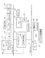
図1には、本発明の一実施形態に係るコンピュータシステムの構成が示されている。このコンピュータシステムは、ノートブックタイプまたはサブノートタイプのポータブルパーソナルコンピュータであり、コンピュータ本体と、このコンピュータ本体に開閉自在に取り付けられたLCDパネルユニットとから構成されている。このコンピュータは、内蔵バッテリを有しており、その内蔵バッテリからの電力によって動作可能に構成されている。また、ACアダプタを介してAC商用電源などの外部電源から電力供給を受けることもできる。外部電源から電力供給を受けているときは、その外部電源からの電力がコンピュータシステムの動作電源として用いられる。このとき、外部電源からの電力によって内蔵バッテリの充電も自動的に行われる。ACアダプタが取り外されたり、あるいはAC商用電源のブレーカが落とされたときなどは、内蔵バッテリからの電力がコンピュータシステムの動作電源として用いられる。
【0014】
また、このコンピュータには、CPU11、CPUバス1とPCIバス2間をつなぐホスト−PCIブリッジ12、主メモリ13、VGAコントローラ14、LANコントローラ15、PCI−ISAブリッジ16、I/Oコントローラ17、ハードディスクドライブ(HDD)18、PCカード19、BIOS−ROM20、埋め込みコントローラ(EC)21、電源コントローラ22などが設けられている。
【0015】
CPU11は、このシステム全体の動作制御およびデータ処理を実行する。このCPU11としては、システム管理割り込みSMI(SMI;System Management Interrupt)をサポートするもの、例えば、米インテル社により製造販売されているマイクロプロセッサ“Pentium”などが使用される。この場合、CPU11は、次のようなシステム管理機能を持つ。
【0016】
すなわち、CPU11は、アプリケーションプログラムやオペレーティングシステム(OS)などのプログラムを実行するための動作モードとしてリアルモード、プロテクトモード、仮想8086モードを有する他、システム管理モード(SMM;System Management mode)と称されるシステム管理機能を実現するための動作モードを有している。
【0017】
リアルモードは、最大で1Mバイトのメモリ空間をアクセスできるモードであり、論理アドレスから物理アドレスへの変換は、セグメントレジスタで表されるベースアドレスからのオフセット値で物理アドレスを決定するアドレス計算形式によって行われる。
【0018】
一方、プロテクトモードは1タスク当たり最大4Gバイトのメモリ空間をアクセスできるモードであり、ディスクプリタテーブルと称されるアドレスマッピングテーブルを用いてリニアアドレスが決定される。このリニアアドレスは、ページングによって最終的に物理アドレスに変換される。
このように、プロテクトモードとリアルモードとでは、互いに異なるメモリアドレッシングが採用されている。
【0019】
システム管理モード(SMM)は疑似リアルモードであり、このモードにおけるアドレス計算形式はリアルモードのアドレス計算形式と同一であり、ディスクプリタテーブルは参照されず、ページングも実行されない。しかし、SMMでは、プロテクトモードと同様に、1Mバイトを越えるメモリ空間をアクセスすることができる。
【0020】
システム管理割込み(SMI;System Management Interrupt)がCPU11に発行された時、CPU11の動作モードは、その時の動作モードであるリアルモード、プロテクトモード、または仮想8086モードから、SMMにスイッチされる。SMIによってSMMにスイッチした時、CPU11はその時のCPUレジスタの内容であるCPUステータスを主メモリ13上のオーバレイメモリ(SMRAMと称される)にセーブする。また、SMMにおいて復帰命令(RSM命令)が実行されると、CPU11はSMRAMからCPUレジスタにCPUステータスをリストアし、SMI発生前の動作モードに復帰する。本実施形態においては、SMMにおいて、BIOSのシステム管理プログラム(サスペンド処理ルーチンおよびレジューム処理ルーチンなど)が実行される。サスペンド処理ルーチンは、OSとの共同作業により、システムステートをサスペンド状態(パワーセーブモード)に設定するためのものであり、CPUコンテクストおよび各種デバイスのステートなどを含むシステムデータを主メモリ13にセーブした後に、主メモリ13を除く他のほとんどのデバイスをパワーオフする(メモリサスペンド)。レジュームルーチンは、OSとの共同作業により、システムをメモリサスペンド前の動作状態に復元させるためのものであり、ウェイクアップイベントが発生したときに、主メモリ13にセーブされているシステムデータを元のCPU11および各デバイスにリストアする。
【0021】
SMIはマスク不能割込みNMIの一種であるが、通常のNMIやマスク可能割込みINTRよりも優先度の高い、最優先度のハードウェア割り込みである。
このSMIを発行することによって、実行中のオペレーティングシステムの環境に依存せずにBIOSを起動することができる。
【0022】
ホスト−PCIブリッジ12はCPUバス1とPCIバス2間を双方向でつなぐブリッジであり、ここには主メモリ13を制御するためのメモリコントローラも内蔵されている。主メモリ13はこのシステムの主記憶つまりシステムメモリとして使用されるものであり、オペレーティングシステム、処理対象のアプリケーションプログラム、およびアプリケーションプログラムによって作成されたユーザデータ等が格納される。この主メモリ13はDRAMなどの半導体メモリによって実現されている。
【0023】
主メモリ13はこのシステムの主記憶つまりシステムメモリとして使用されるものであり、オペレーティングシステム、処理対象のアプリケーションプログラム、およびアプリケーションプログラムによって作成されたユーザデータ等が格納される。この主メモリ13はDRAMなどの半導体メモリによって実現されている。前述のSMRAM(System Management RAM)は、図2に示すように、主メモリ13を構成する物理メモリの一部に割り当てられた記憶空間であり、SMI信号がCPU11に入力された時だけメモリアドレスがマッピングされてアクセス可能となる。ここで、SMRAMがマッピングされるアドレス範囲は固定ではなく、SMBASEと称されるCPU11内のレジスタによって4Gバイト空間の任意の場所に変更することが可能である。SMBASEレジスタは、SMM中でないとアクセスできない。
【0024】
CPU11がSMMに移行する時には、CPUコンテクスト(CPUステータス)、つまりSMIが発生された時のCPU11のレジスタ等が、SMRAMにスタック形式でセーブされる。このSMRAMには、BIOS−ROM20のシステム管理プログラムを呼び出すためのJUMP命令が格納されている。このJUMP命令は、CPU11がSMMに入った時に最初に実行される命令であり、この命令実行によってBIOSのシステム管理プログラムに制御が移る。先ず、SMIハンドラによってSMI発生要因がチェックされる。そして、SMI発生要因に対応するシステム管理プログラムのサービスルーチンの実行がSMIハンドラによってリクエストされる。
【0025】
BIOS−ROM20は、BIOS(Basic I/O System)を記憶するためのものであり、プログラム書き替えが可能なようにフラッシュメモリによって構成されている。BIOSは、このシステム内の各種ハードウェアをアクセスするためのファンクション実行ルーチンを体系化したものであり、リアルモードで動作するように構成されている。
【0026】
このBIOSには、システムのパワーオン時に各種デバイスの初期化及びテストを行うIRTルーチンと、各種ハードウェア制御のためのBIOSドライバ群などが含まれている。各BIOSドライバは、ハードウェア制御のための複数の機能をオペレーティングシステムやアプリケーションプログラムに提供するためにそれら機能に対応する複数のファンクション実行ルーチン群を含んでいる。
【0027】
また、BIOS−ROM20には、前述のシステム管理プログラムなど、SMMの中で実行されるプログラムも格納されている。SMIハンドラは、前述したように、SMIの発生要因に応じて各種SMIサービスルーチンを起動するためのものである。なお、前述のサスペンド処理ルーチンなどはACPI対応のOSから直接起動することもできる。
【0028】
EC21は、システムが持つ付加機能を制御するためのコントローラであり、CPU周辺温度などに応じてクーリングファンの回転制御などを行うための熱制御機能、システムの各種状態をLEDの点灯やビープ音によってユーザに通知するためのLED/ビープ音制御機能、電源コントローラ22と共同してシステム電源のオン/オフなどを制御する電源シーケンス制御機能、および電源ステータス通知機能などを有している。電源ステータス通知機能は、電源コントローラ22と共同してBIOSのレジューム処理ルーチンの起動要因となるウェイクアップイベントの発生を監視し、イベント発生時にそれをSMIなどを用いてBIOSに通知するという機能である。ウェイクアップイベントとしては、電源スイッチ23のオン、パネルスイッチ24のオンなどがある。メモリサスペンド状態においても、EC21および電源コントローラ22には動作電源が供給されており、EC21の各機能は有効である。
【0029】
EC21は、BIOSとの通信のためのI/Oポートを有している。BIOSは、このI/Oポートを介してEC21内のコンフィグレーションレジスタに対してリード/ライトを行うことにより、監視および通知すべきイベントの種類の設定や、発生したイベントを示すステータスのリードなどを行うことができる。
EC21と電源コントローラ22間の通信はI2Cバスを介して行われる。
【0030】
VGAコントローラ14は、このシステムのディスプレイモニタとして使用されるLCDや外部CRTを制御するためのものであり、VRAMに描画された画面データをLCDや外部CRTに表示する。LANコントローラ15は、本システムをLANに接続するためのネットワークインターフェースである。I/Oコントローラ17は各種I/Oデバイスとのインタフェースであり、ハードディスクドライブ(HDD)18を制御するためのIDEインタフェース、PCカード19を制御するためのPCMCIA/CARDBUSインタフェースなどを内蔵している。
【0031】
PCI−ISAブリッジ16はPCIバス2とISAバス3間を双方向でつなぐブリッジであり、ここにはSMI発生回路161が内蔵されている。SMI発生回路161は、図3に示すように、ソフトウェアSMI発生回路201、I/OトラップSMI発生回路202、その他のSMI発生回路204、OR回路204、タイマレジスタ205、ステータスレジスタ206などから構成されている。ソフトウェアSMI発生回路201は、タイマレジスタ205にセットされたインターバル時間で指定される所定の時間間隔でSMI信号(ソフトウェアSMI)を発生する。タイマレジスタ205はプログラム可能であり、ソフトウェアによって任意のインターバル時間をタイマレジスタ205にセットすることができる。本実施形態では、BIOSによるレジューム処理とOSによるレジューム処理とを交互に切り替えながら実行させるために、ソフトウェアSMIが用いられる。ステータスレジスタ206はSMI発生要因を保持するためのものであり、OR回路204を通じてCPU11に供給されたSMIが、ソフトウェアSMI発生回路201、I/OトラップSMI発生回路202、その他のSMI発生回路204のいずれによるものであるかを記憶する。EC21からのイベント通知は、その他のSMI発生回路204経由で発生されるSMIによってCPU11に伝達される。
【0032】
次に、図4を参照して、本システムのモード遷移について説明する。
本システムはACPI仕様に準拠したパワーセーブモードをサポートしている。ACPI仕様では、S0からS5までのシステムステートが定義されている。
S0は動作状態(つまりシステムの電源が入っており、ソフトウェアが実行中の状態)、S5はオフ状態(つまり全てのソフトウェアの実行は終了し、システムの電源が切られている状態)であり、S1〜S4はその中間の状態(スリープ状態と呼ぶ、つまり直前までのソフトウェアの実行状態を保持しつつ動作が停止している状態)である。S1〜S4のうち、本実施形態ではS3とS4をそれぞれメモリサスペンド状態、ハイバネーション状態としてサポートする。
【0033】
つまり、S3では主メモリ13(および一部のチップセット)の電源のみを保持する。つまり主メモリ13(および一部のチップセット)の内容のみが保持される。必要な消費電力は少なくなり、バッテリ駆動状態でスリープ状態(パワーセーブモードの状態)を長時間持続させることができる。
【0034】
S4ではハードディスク18に主メモリ13等の内容が全て保存され、システムの電源は全て切られる。スリープ中の消費電力は最小(S5の状態に等しい)だが、S0へ戻るのに最も時間がかかる。つまり最も「深い」スリープ状態である。
【0035】
さらに、ACPI仕様では、デバイスパワーマネージメントのためのステートして、D0からD3までのステート(デバイスパワーステート)を定義している。デバイスパワーマネージメントはバス上のデバイスに関するパワーマネージメントである。各デバイスは最低D0とD3の2つの状態をサポートすることが要求されている。D0はデバイスが完全にアクティブの動作ステートであり、またD3は電源オフ状態と同等の省電力ステートである。
【0036】
システムステートがS0からS3のメモリサスペンド状態に遷移するとき、それに合わせて各デバイスのデバイスステートもそれまでのステート(通常はD0)から省電力ステートであるD3に遷移される。デバイスステートD3への遷移はOSの制御の下に実行され、D3状態に遷移したデバイスのレジスタ等のステータスを主メモリ13にセーブする処理はBIOSによって実行される。
【0037】
次に、図5を参照して、S0の動作状態からS3のメモリサスペンド状態に遷移する時に実行される一連の処理の流れについて説明する。
GUIによるコマンド入力または電源スイッチのオフ操作などによってユーザからOSに対してサスペンド(スタンバイ)の指示がなされると、OSは、現在の作業を問題なく中断するために必要な処理(OSサスペンド処理)を開始する(ステップS101)。ここでは、例えばネットワーク接続環境などの現在の状態を主メモリ13またはHDD18などに保存するなどの処理も行われる。次いで、OSは、システム内の各デバイスをD0からD3に遷移させるための処理を行う(ステップS102)。全てのデバイスがD3に遷移した後、OSからのリクエストにより、BIOSのサスペンド処理ルーチンが起動される。
【0038】
サスペンド処理ルーチンは、CPU11およびホスト−PCIブリッジ12などのコアデバイスの内部ステータスをシステムデータとして主メモリ13にセーブし(ステップS103)、次いで、D3に設定されている各デバイスのステータスを主メモリ13にセーブする(ステップS104)。この後、サスペンド処理ルーチンは、EC21を通じて電源コントローラ22を制御することにより、主メモリ13(および一部のチップセット)を除く他のほとんどのデバイスをパワーオフする(ステップS104)。
【0039】
次に、図6を参照して、S3のメモリサスペンド状態からS0の動作状態に復帰する時に実行される一連の処理の流れについて説明する。
電源スイッチ23のオン操作などのウェイクアップイベントが発生すると、BIOSのレジュームルーチンが実行される。BIOSのレジュームルーチンは、まず、主メモリ13にセーブされているシステムデータをCPU11およびホスト−PCIブリッジ12などのコアデバイスにリストアすることにより、OSの動作に最低限必要なコアデバイスの復帰処理(コアデバイス復帰)を実行する(ステップS111)。次いで、BIOSのレジュームルーチンは、主メモリ13にセーブされている各デバイスのデータをリストアすることにより、各デバイスをD3の状態に復帰させるための処理(D3復帰処理)を実行する(ステップS112)。このステップS112のD3復帰処理は、各デバイスをD3からD0の状態に復帰させるというステップS113の処理(D0復帰)と並行して実行される。D0復帰処理は、OSによって実行される。全てのデバイスについてのD0復帰処理が終了した後、OSは、そのOSの作業環境をメモリサスペンド前と同じ状態にするための残りのレジューム処理を行う(ステップS114)。ここでは、例えばネットワークの再接続などの処理や、BIOSによって管理されないオプションデバイスに関する復帰処理などが実行される。
【0040】
すなわち、複数のデバイスそれぞれに関するレジューム処理はD3復帰とD0復帰の2段階で行われる。本実施形態では、これらD3復帰処理とD0復帰処理との並行処理により、D3復帰が完了したデバイスから順にD0復帰を開始できるようにしている。
【0041】
この並行処理の原理を図7に示す。図7(a)は従来の順次処理を示し、図7(b)は本実施形態の並行処理を示している。図7(b)から分かるように、本実施形態では、BIOSによるレジューム処理をコアデバイスの復帰処理と他の各デバイスに関するD3復帰処理とに分割しており、コアデバイスの復帰処理が完了した時点で、OSによるレジューム処理を開始させるようにしている。BIOSによるD3復帰処理は、OSによるD0復帰処理中にソフトウェアSMIを定期的に発行すること等によって割り込み処理の形式で実行される。これにより、D3復帰処理とD0復帰処理とが時分割的に交互に実行されることになり、全てのデバイスについてのD3復帰処理が完了してからD0復帰処理に移行するという従来の順次処理に比べ、レジューム処理全体に要する時間を短縮することができる。
【0042】
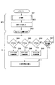
図8には、D3復帰処理とD0復帰処理との並行処理の様子が模式的に示されている。
図8では、BIOSによるD3復帰処理がデバイスA,B,Cの順で完了し(ステップS201,S202,S203)、D3復帰処理が完了したデバイスから順にOSによるD0復帰処理(ステップS211,S212,S213)が実行される様子が示されている。D3復帰処理は、D0復帰処理を正常に行うために必要な前処理である。このため、図8のように、D3復帰処理が完了したデバイスから順にD0復帰処理を行うことにより、不具合を招くことなく、各デバイスをD0ステートに正常に復帰させることができる。
【0043】
なお、D3復帰処理およびD0復帰処理のどちらにおいても、各デバイスに対してはレジスタ値の設定などのためのコマンドが順次発行されることになる。コマンド毎にI/O待ちが発生するので、あるデバイスに対するI/O待ちの時間を利用して他のデバイスに対する処理を行うことにより、さらにレジューム処理の効率化を図ることができる。これを実現するため、本実施形態では、複数のデバイスそれぞれに対するD3復帰処理を並行して実行するようにしている。この様子を図9に示す。
【0044】
図9においては、デバイスA,B,Cに関するD3復帰処理を並行して行い、且つこのD3復帰処理とOSによるD0復帰処理が並行して行われる様子が示されている。すなわち、BIOSは、まず、デバイスAにコマンドを発行し(ステップS301)、そのデバイスAのコマンド処理待ちの間に、デバイスBにコマンドを発行する(ステップS302)。同様に、このデバイスBのコマンド処理待ちの間に、デバイスCにコマンドを発行する(ステップS302)。このような処理は、割り込み処理によってOSからBIOSに制御が移されるたびに、D3復帰処理が完了していないデバイスそれぞれに対して実行される。図9では、説明を簡単にするために、デバイスAについては一回のコマンド処理(A1)でD3復帰処理が完了し、デバイスBについては3回のコマンド処理(B1〜B3)でD3復帰処理が完了し、そしてデバイスCについては3回のコマンド処理(B1〜B3)でD3復帰処理が完了する場合を示している。
【0045】
OSのD0復帰処理では、デバイスA,B,CそれぞれについてD3復帰処理が完了しているかどうかがチェックされ(ステップS401〜S403)、D3復帰処理が完了してレディー状態となったデバイスから順にD0復帰処理が実行される(ステップS404,S405,S406)。各デバイスのD0復帰処理においてもコマンド終了待ち(I/O待ち)が発生する。このため、もしそのコマンド終了待ちの期間中にソフトウェアSMIが発生すれば、あるデバイスに関するD0復帰のためのコマンド処理と並行して、別のデバイスに関するD0復帰のためのコマンド処理が実行されることになる。つまり、デバイスA,B,Cに着目すれば、それらは同時並行的にコマンド処理を実行することになる。
【0046】
次に、図10のフローチャートを参照して、レジューム処理の手順について具体的に説明する。
BIOSは、まず、前述のコアデバイス復帰処理を実行する(ステップS501)。次に、BIOSは、ソフトウェアSMIの発生準備のために、タイマレジスタ205に所定のインターバルタイマ値(SMIタイマ)をセットした後(ステップS502)、主メモリ13上に存在するOSレジューム処理の先頭コードにジャンプしてOSに制御を渡す(ステップS503)。
【0047】
OSは、そのレジューム処理のメインルーチンの中で、デバイスA,B,CそれぞれについてD3復帰処理が完了しているかどうか、および全デバイスのD0復帰処理が完了したかをサイクリックにチェックする(ステップS504,S505,S506.S507)。例えばデバイス毎にビジーステータスフラグを用意し、D3復帰処理が完了したデバイス毎にBIOSが対応するビジーステータスフラグをリセットするなどの仕組みを用いれば、OSは、該当するデバイスに対応するビジーステータスフラグをチェックするだけでD3復帰処理が完了しているかどうかを容易に判別することができる。ステップS504,S505,S506.S507の手順は、例えばACPI用に用意されたマクロであるASL等によってOSに記述しておけばよい。
【0048】
そして、OSは、D3復帰処理が完了したデバイスから順にD0復帰処理のためのコマンド発行を行う(ステップS508〜S510)。全デバイスのD0復帰処理が完了すると、OSは、必要なネットワーク再接続などの処理を行って、サスペンド前のOS作業環境を復元する(ステップS511)。
【0049】
以上のOSレジューム処理の期間には定期的にソフトウェアSMIが発生し、そのたびにBIOSに制御が移される。BIOSは、SMI割り込み処理の中で図11に示す処理を実行する。
【0050】
すなわち、BIOSは、まず、デバイスAに関するD3復帰処理が全て完了しているか否かをチェックし(ステップS611)、完了してなければ、デバイスAに関するD3復帰処理を実行する(ステップS612)。デバイスAのD3復帰処理に例えば3つのコマンド処理(処理#1,#2,#3)が必要な場合、ステップS612では、各処理毎にそれが実行済みであるどうかをチェックし、未実行であればそれを実行するという処理が行われる。一つのコマンド処理を行うたびに、BIOSは、ステップS612の処理から抜ける。
【0051】
デバイスAに関するD3復帰処理が全て完了している場合、あるいはステップS612にてデバイスAに関する一つのコマンド処理を実行したならば、BIOSは、今度は、デバイスBに関するD3復帰処理が全て完了しているか否かをチェックし(ステップS613)、完了してなければ、デバイスBに関するD3復帰処理を実行する(ステップS614)。このステップS614でも、ステップS612と同様に、各コマンド処理毎にそれが実行済みであるどうかをチェックしながら、未実行のコマンド処理を実行する。一つのコマンド処理を行うたびに、BIOSは、ステップS614の処理から抜ける。
【0052】
以上のような処理が各デバイス毎に行われた後、BIOSは、全てのデバイスについてのD3復帰処理が全て完了したか否かをチェックする(ステップS615)。完了していない場合には、そのままSMMを抜けて、割り込み元のOSに制御を戻す。一方、全てのデバイスについてのD3復帰処理が全て完了した場合には、タイマレジスタ205のインターバルタイマ値(SMIタイマ)をリセットして、ソフトウェアSMIの発生を停止させた後(ステップS615)、SMMを抜けて、割り込み元のOSに制御を戻す。
【0053】
以上のようにして、BIOSとOSが交互に実行されながら、複数のデバイスそれぞれのD3復帰とD0復帰のための処理が並行して進められる。
【0054】
なお、これまでの説明ではOSからBIOSへの切り換えをソフトウェアSMIで行う場合についてのみ説明したが、D3復帰のためのコマンド処理の完了を示すデバイスからの割り込み信号をSMIに変換することにより、OSからBIOSへの切り換えをデバイスからの割り込み信号によって行うこともできる。そのためのハードウェア構成の一例を図12に示す。
【0055】
図12に示されているように、通常は、デバイス301〜303それぞれからの割り込み信号(IRQまたはINT)は割り込みコントローラ304を介してCPU11にマスク可能割込みINTRなどとして供給される。OSのレジューム処理に影響を与えることなく、BIOSのレジューム処理を割り込み処理によって実行するためにはSMMモードを利用することが好ましい。このため、本例では、割り込み信号変換回路305、ステータスレジスタ306、イネーブル/ディスエーブルレジスタ307が設けられている。割り込み信号変換回路305は、デバイス301〜303それぞれからの割り込み信号(IRQまたはINT)をSMI信号に変換し、それをデバイスSMIとしてOR回路204に出力する。割り込み信号変換回路305の変換動作は、イネーブル/ディスエーブルレジスタ307の設定値によって許可又は禁止される。現在のデバイスSMIがどのデバイスからの割り込み信号に起因するものであるかは、ステータスレジスタ306を参照することによって判別できる。
【0056】
以下、図13のフローチャートを参照して、デバイスSMIを利用する場合におけるレジューム処理の手順を説明する。
【0057】
BIOSは、まず、コアデバイス復帰処理を実行する(ステップS701)。
次に、BIOSは、イネーブル/ディスエーブルレジスタ307をイネーブルフラグをセットして、デバイスSMIの発生を有効にする(ステップS702)。
この後、BIOSは、デバイスA,B,Cそれぞれに対してD3復帰に必要なコマンド発行を一回ずつ実行した後(ステップS703)、主メモリ13上に存在するOSレジューム処理の先頭コードにジャンプしてOSに制御を渡す(ステップS704)。そして、OSによるレジューム処理が開始される(ステップS705)。このOSレジューム処理では、図10のステップS504〜S511で説明した処理が行われる。ただし、各デバイスからの割り込み信号はBIOS起動のためのデバイスSMIとして利用されているので、D0復帰のためのコマンド処理が終了したか否かのチェックは該当するデバイスをポーリングすることによって行われることになる。
【0058】
D3復帰のためのコマンド処理が終了したデバイスから割り込み信号が発生すると、デバイスSMIによってBIOSが起動される。BIOSは、ステータスレジスタ306を参照することによってデバイスSMIの要因が、デバイスAによるデバイスSMI(デバイスA_SMI)、デバイスBによるデバイスSMI(デバイスB_SMI)、デバイスCによるデバイスSMI(デバイスC_SMI)のいずれであるかを判定する。BIOSにはデバイスA,B,Cそれぞれに対応するSMI処理ルーチンが設けられており、デバイスSMIの発生要因に対応するSMI処理ルーチンが実行される。
【0059】
例えば、デバイスAに対応するSMI処理ルーチンの場合には、デバイスAのD3復帰に必要な次のコマンド発行を一回実行する(ステップS711)。次いで、全デバイスに関するD3復帰処理の完了の有無をチェックし(ステップS712)、完了していない場合には、そのままSMMを抜けて、割り込み元のOSに制御を戻す。一方、全てのデバイスについてのD3復帰処理が全て完了した場合には、イネーブル/ディスエーブルレジスタ307のイネーブルフラグをリセットして、デバイスSMIを無効化した後(ステップS712)、SMMを抜けて、割り込み元のOSに制御を戻す。デバイスBに対応するSMI処理ルーチンでも同様の処理(ステップS721〜S723)が実行され、またデバイスCに対応するSMI処理ルーチンでも同様の処理(ステップS731〜S733)が実行される。
【0060】
以上のように、本実施形態のレジューム処理方法によれば、BIOSレジューム処理とOSレジューム処理を並行処理することで、レジューム処理の高速化を図ることが可能となる。
【0061】
なお、本発明は、上記実施形態に限定されるものではなく、実施段階ではその要旨を逸脱しない範囲で種々に変形することが可能である。更に、上記実施形態には種々の段階の発明が含まれており、開示される複数の構成要件における適宜な組み合わせにより種々の発明が抽出され得る。例えば、実施形態に示される全構成要件から幾つかの構成要件が削除されても、発明が解決しようとする課題の欄で述べた課題が解決でき、発明の効果の欄で述べられている効果が得られる場合には、この構成要件が削除された構成が発明として抽出され得る。
【0062】
【発明の効果】
以上説明したように、本発明によれば、レジューム処理を高速に実行できるようになり、サスペンドなどのパワーセーブモードからの復帰に要する時間を短縮する事が可能となる。
【図面の簡単な説明】
【図1】本発明の一実施形態に係るコンピュータシステムの構成を示すブロック図。
【図2】同実施形態におけるBIOSレジュームルーチンの起動処理動作の一例を説明するための図。
【図3】同実施形態で用いられるSMI発生回路の構成を示す図。
【図4】同実施形態のシステムステートの遷移の様子を示す図。
【図5】同実施形態のシステムがメモリサスペンド状態に遷移する時に実行される一連の処理の流れを説明するフローチャート。
【図6】同実施形態のシステムがメモリサスペンド状態から復帰する時に実行される一連の処理の流れを説明するフローチャート。
【図7】同実施形態のシステムで実行されるBIOSレジューム処理とOSレジューム処理との並行処理の原理を説明するための図。
【図8】同実施形態のシステムで実行されるD3復帰処理とD0復帰処理との並行処理の様子を示す図。
【図9】同実施形態のシステムにおいて複数のデバイスに関するD3復帰処理を並行して行う場合の処理例を示す図。
【図10】同実施形態のシステムで実行されるレジューム処理の手順を示すフローチャート。
【図11】同実施形態のシステムで実行されるBIOSレジューム処理の手順を示すフローチャート。
【図12】同実施形態のシステムでデバイスSMIを利用する場合のハードウェア構成の一例を示すブロック図。
【図13】同実施形態のシステムで実行されるレジューム処理の手順の他の例を示すフローチャート。
【符号の説明】
11…CPU
12…ホスト−PCIブリッジ
13…主メモリ
15…LANコントローラ
20…BIOS−ROM
201…ソフトウェアSMI発生回路
205…タイマレジスタ
305…割り込み信号変換回路[0001]
BACKGROUND OF THE INVENTION
The present invention relates to a computer system and a resume processing method used in the system, and more particularly to a computer system capable of quickly returning from a power save mode to a normal operation mode and a resume processing method used in the system.
[0002]
[Prior art]
In recent years, various portable notebook-type or sub-notebook-type personal computers and pocket computers such as portable information terminals have been developed.
[0003]
This type of portable computer is provided with various power saving modes (sleep modes) for conserving power of the computer system in order to extend the battery-operable time. The suspend mode is one of the sleep modes with the least power consumption. That is, when the computer system is in the suspend mode, most other devices in the system are powered off except for the main memory where system data necessary for restarting the operating system and user programs is saved.
[0004]
The system data saved in the main memory is the status of the CPU and the status of various devices immediately before the computer system is set to the suspend mode. The main memory also stores the operating state of the operating system and application program and user data created by the application program. When the system is powered on again after the suspend, the system data saved in the main memory is restored, thereby restoring the working state immediately before the suspend mode (resume).
[0005]
The system data is saved by a suspend routine incorporated in the system BIOS (basic input / output program). The system BIOS is for controlling hardware in the system according to a request from the operating system, and includes a device driver group for controlling various hardware devices in the system. The system BIOS suspend routine is activated when the system is powered off, etc., saves the CPU registers and various peripheral LSI statuses in the memory, and then powers off the system.
[0006]
Power to the main memory is maintained by the battery throughout the system power off. For this reason, the system status and user data are not lost, and the system can be returned to the working state before the suspension at high speed.
[0007]
[Problems to be solved by the invention]
However, recently, as represented by ACPI (Advanced Configuration and Power Interface), a technology has been developed that allows the operating system (OS) itself to have a management function related to system power saving. Suspend / resume processing is Under the management of the OS, it has come to be performed jointly between the OS and the BIOS. In this case, the resume process is executed in two stages: a resume process by the BIOS and a resume process by the OS. In the resume process by the BIOS, a return process to a state in which the operation of the OS and each device under the OS management can be guaranteed is executed. Thereafter, control is transferred from the BIOS to the OS, and resume processing by the OS is executed. By the resume process by the OS, each device is restored to the same original operation state as before the suspension.
[0008]
However, since a computer system is usually composed of a large number of devices, the BIOS resume processing is already completed in the conventional sequential processing in which the resume processing of the OS is completed after completion of the BIOS resume processing for all devices. Even if there is a device that is operating, the resume processing of the OS cannot be started. For this reason, a wasteful waiting time is generated, and a relatively long time is required for restoring the system state.
[0009]
The present invention has been made in view of the above-described circumstances, and enables a resume process to be executed at high speed and a computer system and a suspend process method capable of reducing the time required to return from a power save mode such as suspend. The purpose is to provide.
[0010]
[Means for Solving the Problems]
In order to solve the above-described problem, the present invention provides a computer system having a resume processing function for restoring a work environment immediately before the power save mode using system data saved in a memory when shifting to the power save mode. Of the first resume process to be executed by the BIOS program to execute the resume process function at the time of wake-up from the power save mode, the system core unit including the CPU necessary for the operation of the operating system Means for causing the BIOS program to execute processing for restoring the state using the system data saved in the memory, and for restoring the state of the system core unit including the CPU , Each provided for each device Responsive to completion of processing, control should be transferred from the BIOS program to the operating system and executed by the operating system to perform the resume processing function Provided for each device Means for causing the operating system to execute a second resume process, a remaining process of the first resume process, and the second resume process. Alternately Interrupt control means for inserting an interrupt process during a period in which the operating system is executing the second resume process and executing the BIOS program in the interrupt process so as to be executed. It is characterized by.
[0011]
In this computer system, the first resume process executed by the BIOS program is divided into two, and the state of the system core part necessary for the operation of the operating system is restored in the first resume process. When the processing portion is completed, control is transferred from the BIOS program to the operating system. Thereafter, an interrupt process is inserted during the period when the second resume process is being executed, and the BIOS program is executed in the interrupt process, whereby the remaining part of the first resume process is executed. The second resume process by the operating system is executed in parallel. As a result, the second resume process can be started without waiting for the completion of the first resume process for all the devices. Therefore, after the first resume process of the BIOS for all the devices is completed, the second resume of the operating system is completed. Compared to the conventional sequential process of shifting to the resume process, the time required for the entire resume process can be shortened.
[0012]
In general, in order to restore the state of a device, it is necessary to issue a command to the device many times as in the case of initialization processing, and the device performs command processing each time the command is issued. I / O waiting to wait until the completion of the process occurs. The penalty for waiting for I / O can be greatly reduced by parallel processing of the remaining part of the first resume process and the second resume process by the operating system.
[0013]
DETAILED DESCRIPTION OF THE INVENTION
Hereinafter, embodiments of the present invention will be described with reference to the drawings.
FIG. 1 shows the configuration of a computer system according to an embodiment of the present invention. This computer system is a notebook-type or sub-notebook-type portable personal computer, and is composed of a computer main body and an LCD panel unit attached to the computer main body so as to be freely opened and closed. This computer has a built-in battery, and is configured to be operable by electric power from the built-in battery. In addition, power can be supplied from an external power source such as an AC commercial power source via an AC adapter. When power is supplied from an external power source, the power from the external power source is used as an operating power source for the computer system. At this time, the built-in battery is automatically charged by the power from the external power source. When the AC adapter is removed or the AC commercial power supply breaker is turned off, the power from the built-in battery is used as the operating power supply for the computer system.
[0014]
The computer includes a
[0015]
The
[0016]
That is, the
[0017]
The real mode is a mode in which a memory space of 1 Mbyte at the maximum can be accessed, and conversion from a logical address to a physical address is performed by an address calculation format that determines a physical address with an offset value from a base address represented by a segment register. Done.
[0018]
On the other hand, the protect mode is a mode in which a memory space of up to 4 Gbytes per task can be accessed, and a linear address is determined using an address mapping table called a descriptor table. This linear address is finally converted into a physical address by paging.
Thus, different memory addressing is employed in the protect mode and the real mode.
[0019]
The system management mode (SMM) is a pseudo real mode. The address calculation format in this mode is the same as the address calculation format in the real mode, and the descriptor table is not referred to and paging is not executed. However, in SMM, a memory space exceeding 1 Mbytes can be accessed as in the protect mode.
[0020]
When a system management interrupt (SMI) is issued to the
[0021]
The SMI is a kind of non-maskable interrupt NMI, but is a highest priority hardware interrupt having a higher priority than a normal NMI or maskable interrupt INTR.
By issuing this SMI, the BIOS can be activated without depending on the environment of the operating system being executed.
[0022]
The host-
[0023]
The
[0024]
When the
[0025]
The BIOS-
[0026]
The BIOS includes an IRT routine for initializing and testing various devices when the system is powered on, and a BIOS driver group for various hardware control. Each BIOS driver includes a plurality of function execution routine groups corresponding to these functions in order to provide a plurality of functions for hardware control to the operating system and application programs.
[0027]
The BIOS-
[0028]
The
[0029]
The
Communication between EC21 and
[0030]
The
[0031]
The PCI-
[0032]
Next, the mode transition of this system will be described with reference to FIG.
The system supports a power save mode that conforms to the ACPI specification. In the ACPI specification, system states from S0 to S5 are defined.
S0 is the operating state (that is, the system is turned on and the software is running), S5 is the off state (that is, the execution of all the software is finished, and the system is turned off), S1 to S4 are intermediate states (called a sleep state, that is, a state in which the operation is stopped while maintaining the execution state of the software up to immediately before). Among S1 to S4, this embodiment supports S3 and S4 as a memory suspend state and a hibernation state, respectively.
[0033]
That is, in S3, only the power source of the main memory 13 (and some chip sets) is held. That is, only the contents of the main memory 13 (and some chip sets) are retained. The required power consumption is reduced, and the sleep state (power save mode state) can be maintained for a long time in the battery drive state.
[0034]
In S4, the contents of the
[0035]
Further, in the ACPI specification, states (device power states) from D0 to D3 are defined as states for device power management. Device power management is power management for devices on the bus. Each device is required to support at least two states, D0 and D3. D0 is an operating state in which the device is completely active, and D3 is a power saving state equivalent to the power-off state.
[0036]
When the system state transitions from the S0 to the memory suspend state of S3, the device state of each device is also transitioned from the previous state (usually D0) to the power saving state D3. The transition to the device state D3 is executed under the control of the OS, and the BIOS saves the status of the registers and the like of the device that has transitioned to the D3 state in the
[0037]
Next, with reference to FIG. 5, a flow of a series of processes executed when the operation state of S0 is changed to the memory suspend state of S3 will be described.
When the user gives a suspend (standby) instruction to the OS by inputting a command using a GUI or turning off the power switch, the OS performs a process necessary for interrupting the current operation without any problem (OS suspend process). Is started (step S101). Here, for example, processing such as saving the current state such as the network connection environment in the
[0038]
The suspend processing routine saves the internal status of core devices such as the
[0039]
Next, a flow of a series of processes executed when returning from the memory suspend state in S3 to the operation state in S0 will be described with reference to FIG.
When a wake-up event such as an ON operation of the
[0040]
That is, the resume process for each of the plurality of devices is performed in two stages, D3 return and D0 return. In the present embodiment, the D0 return can be started in order from the device for which the D3 return is completed by the parallel processing of the D3 return process and the D0 return process.
[0041]
The principle of this parallel processing is shown in FIG. FIG. 7A shows conventional sequential processing, and FIG. 7B shows parallel processing of the present embodiment. As can be seen from FIG. 7B, in the present embodiment, the resume process by the BIOS is divided into the core device return process and the D3 return process for other devices, and the core device return process is completed. Thus, resume processing by the OS is started. The D3 return process by the BIOS is executed in the form of an interrupt process by periodically issuing a software SMI during the D0 return process by the OS. As a result, the D3 return process and the D0 return process are alternately executed in a time-sharing manner, and the conventional sequential process of shifting to the D0 return process after completing the D3 return process for all devices is completed. In comparison, the time required for the entire resume process can be shortened.
[0042]
FIG. 8 schematically shows the parallel processing of the D3 return processing and the D0 return processing.
In FIG. 8, the D3 return processing by the BIOS is completed in the order of devices A, B, and C (steps S201, S202, and S203), and the D0 return processing by the OS (steps S211, S212, and S212, from the devices that have completed the D3 return processing). The manner in which S213) is executed is shown. The D3 return process is a pre-process necessary for normally performing the D0 return process. For this reason, as shown in FIG. 8, by performing the D0 return processing in order from the device for which the D3 return processing has been completed, each device can be normally returned to the D0 state without causing problems.
[0043]
In both the D3 return process and the D0 return process, commands for setting register values and the like are sequentially issued to each device. Since an I / O wait occurs for each command, the efficiency of the resume process can be further improved by performing the process for another device using the I / O wait time for a certain device. In order to realize this, in this embodiment, the D3 return processing for each of a plurality of devices is executed in parallel. This is shown in FIG.
[0044]
FIG. 9 shows a state in which the D3 return processing for the devices A, B, and C is performed in parallel, and the D3 return processing and the D0 return processing by the OS are performed in parallel. That is, the BIOS first issues a command to the device A (step S301), and issues a command to the device B while waiting for command processing of the device A (step S302). Similarly, a command is issued to device C while the device B waits for command processing (step S302). Such processing is executed for each device for which D3 return processing has not been completed each time control is transferred from the OS to the BIOS by interrupt processing. In FIG. 9, in order to simplify the description, the device A completes the D3 return processing by one command processing (A1), and the device B performs the D3 return processing by three command processing (B1 to B3). Is shown, and the device C shows the case where the D3 return processing is completed in three command processes (B1 to B3).
[0045]
In the D0 return processing of the OS, it is checked whether or not the D3 return processing has been completed for each of the devices A, B, and C (steps S401 to S403), and the D0 return processing is completed and the devices that are in the ready state are sequentially D0. A return process is executed (steps S404, S405, S406). In the D0 return processing of each device, a command end wait (I / O wait) occurs. For this reason, if software SMI occurs during the command waiting period, command processing for D0 return for another device is executed in parallel with command processing for D0 return for a certain device. become. In other words, if attention is paid to the devices A, B, and C, they execute command processing in parallel.
[0046]
Next, the resume process will be described in detail with reference to the flowchart of FIG.
First, the BIOS executes the above-described core device return processing (step S501). Next, the BIOS sets a predetermined interval timer value (SMI timer) in the
[0047]
In the main routine of the resume process, the OS cyclically checks whether the D3 return process has been completed for each of the devices A, B, and C, and whether the D0 return process has been completed for all the devices (step S3). S504, S505, S506. S507). For example, if a busy status flag is prepared for each device and a mechanism such as resetting the busy status flag corresponding to the BIOS for each device for which the D3 return processing has been completed is used, the OS sets the busy status flag corresponding to the corresponding device. It is possible to easily determine whether or not the D3 return processing is completed only by checking. Steps S504, S505, S506. The procedure of S507 may be described in the OS using, for example, ASL which is a macro prepared for ACPI.
[0048]
Then, the OS issues commands for the D0 return process in order from the device for which the D3 return process has been completed (steps S508 to S510). When the D0 return processing for all devices is completed, the OS performs necessary network reconnection processing and the like to restore the OS work environment before suspension (step S511).
[0049]
During the period of the above OS resume processing, software SMI is periodically generated, and control is transferred to the BIOS each time. The BIOS executes the process shown in FIG. 11 in the SMI interrupt process.
[0050]
That is, the BIOS first checks whether or not all the D3 return processing relating to the device A has been completed (step S611), and if not completed, executes the D3 return processing relating to the device A (step S612). If, for example, three command processes (
[0051]
If all the D3 return processing relating to device A has been completed, or if one command processing relating to device A has been executed in step S612, the BIOS now completes all D3 return processing relating to device B being completed. It is checked whether or not (step S613), and if not completed, the D3 return processing for the device B is executed (step S614). Also in step S614, as in step S612, unexecuted command processing is executed while checking whether it has been executed for each command processing. Each time one command process is performed, the BIOS exits the process of step S614.
[0052]
After the processing as described above is performed for each device, the BIOS checks whether or not all the D3 return processing for all devices has been completed (step S615). If it is not completed, the SMM is left as it is, and the control is returned to the interrupt source OS. On the other hand, when all the D3 return processing for all devices is completed, the interval timer value (SMI timer) of the
[0053]
As described above, while the BIOS and the OS are alternately executed, the processes for the D3 return and the D0 return of each of the plurality of devices are performed in parallel.
[0054]
In the above description, only the case where the switching from the OS to the BIOS is performed by the software SMI has been described. However, by converting the interrupt signal from the device indicating the completion of the command processing for returning from D3 into the SMI, the OS Switching from BIOS to BIOS can also be performed by an interrupt signal from the device. An example of the hardware configuration for this purpose is shown in FIG.
[0055]
As shown in FIG. 12, normally, an interrupt signal (IRQ or INT) from each of the
[0056]
Hereinafter, with reference to the flowchart of FIG. 13, the procedure of the resume process when using the device SMI will be described.
[0057]
First, the BIOS executes a core device return process (step S701).
Next, the BIOS sets an enable flag in the enable / disable
After this, the BIOS executes the command issuance necessary for returning to D3 once for each of the devices A, B, and C (step S703), and then jumps to the head code of the OS resume process existing on the
[0058]
When an interrupt signal is generated from a device that has completed command processing for returning from D3, the BIOS is activated by the device SMI. In the BIOS, referring to the
[0059]
For example, in the case of the SMI processing routine corresponding to the device A, the next command issuance necessary for returning the device A to D3 is executed once (step S711). Next, it is checked whether or not the D3 return processing for all devices is completed (step S712). If it is not completed, the SMM is left as it is, and control is returned to the interrupt source OS. On the other hand, when all the D3 return processing for all devices is completed, the enable flag of the enable / disable
[0060]
As described above, according to the resume processing method of the present embodiment, it is possible to increase the speed of the resume process by performing the BIOS resume process and the OS resume process in parallel.
[0061]
In addition, this invention is not limited to the said embodiment, In the implementation stage, it can change variously in the range which does not deviate from the summary. Further, the above embodiments include inventions at various stages, and various inventions can be extracted by appropriately combining a plurality of disclosed constituent elements. For example, even if some constituent requirements are deleted from all the constituent requirements shown in the embodiment, the problem described in the column of the problem to be solved by the invention can be solved, and the effect described in the column of the effect of the invention Can be obtained as an invention.
[0062]
【The invention's effect】
As described above, according to the present invention, the resume process can be executed at high speed, and the time required for returning from the power save mode such as suspend can be shortened.
[Brief description of the drawings]
FIG. 1 is a block diagram showing a configuration of a computer system according to an embodiment of the present invention.
FIG. 2 is an exemplary view for explaining an example of a BIOS resume routine start processing operation in the embodiment;
FIG. 3 is a diagram showing a configuration of an SMI generation circuit used in the embodiment.
FIG. 4 is a view showing a state of system state transition according to the embodiment;
FIG. 5 is an exemplary flowchart illustrating a flow of a series of processing executed when the system according to the embodiment makes a transition to a memory suspend state.
FIG. 6 is an exemplary flowchart illustrating a flow of a series of processing executed when the system according to the embodiment returns from the memory suspend state.
FIG. 7 is an exemplary view for explaining the principle of parallel processing of BIOS resume processing and OS resume processing executed in the system according to the embodiment;
FIG. 8 is an exemplary view showing a state of parallel processing of D3 return processing and D0 return processing executed in the system of the embodiment.
FIG. 9 is a diagram showing a processing example when performing D3 return processing for a plurality of devices in parallel in the system according to the embodiment;
FIG. 10 is an exemplary flowchart illustrating a procedure of resume processing executed in the system according to the embodiment;
FIG. 11 is an exemplary flowchart illustrating a procedure of BIOS resume processing executed in the system according to the embodiment;
FIG. 12 is an exemplary block diagram illustrating an example of a hardware configuration when a device SMI is used in the system according to the embodiment.
FIG. 13 is an exemplary flowchart illustrating another example of the resume process executed in the system according to the embodiment;
[Explanation of symbols]
11 ... CPU
12 ... Host-PCI bridge
13 ... Main memory
15 ... LAN controller
20 ... BIOS-ROM
201: Software SMI generation circuit
205 ... Timer register
305 ... Interrupt signal conversion circuit
Claims (13)
前記パワーセーブモードからのウェイクアップ時に、前記レジューム処理機能の実行のためにBIOSプログラムによって実行されるべき第1のレジューム処理の内で、オペレーティングシステムの動作に必要な、CPUを含むシステムコア部の状態を前記メモリにセーブされたシステムデータを用いて復元するための処理を、前記BIOSプログラムに実行させる手段と、
前記CPUを含むシステムコア部の状態を復元するための、デバイス毎に設けられたそれぞれの処理の完了に応答して、前記BIOSプログラムから前記オペレーティングシステムに制御を移し、前記レジューム処理機能の実行のために前記オペレーティングシステムによって実行されるべき前記デバイス毎に設けられた第2のレジューム処理を、前記オペレーティングシステムに実行させる手段と、
前記第1のレジューム処理の内の残りの処理と前記第2のレジューム処理とが交互に実行されるように、前記オペレーティングシステムが前記第2のレジューム処理を実行している期間中に割り込み処理を挿入し、その割り込み処理の中で前記BIOSプログラムを実行させる割り込み制御手段とを具備することを特徴とするコンピュータシステム。In a computer system having a resume processing function for restoring a work environment immediately before the power save mode using system data saved in a memory at the time of transition to the power save mode,
Of the first resume process to be executed by the BIOS program to execute the resume process function at the time of wake-up from the power save mode, the system core unit including the CPU necessary for the operation of the operating system Means for causing the BIOS program to execute processing for restoring a state using system data saved in the memory;
In response to completion of each process provided for each device for restoring the state of the system core unit including the CPU, control is transferred from the BIOS program to the operating system, and execution of the resume processing function is performed. Means for causing the operating system to execute a second resume process provided for each of the devices to be executed by the operating system for
Interrupt processing is performed during a period in which the operating system is executing the second resume processing so that the remaining processing of the first resume processing and the second resume processing are executed alternately. A computer system comprising: interrupt control means for inserting and executing the BIOS program in the interrupt process.
前記割り込み制御手段は、各デバイスからのコマンド処理の完了を示す割り込み信号に応答して、前記割り込み処理を挿入するための割り込み信号を前記CPUに発行する手段を含むことを特徴とする請求項3記載のコンピュータシステム。In the pre-processing, commands necessary for restoring them to a state where the second resume processing can be performed are sequentially issued to each of the plurality of devices.
4. The interrupt control means includes means for issuing an interrupt signal for inserting the interrupt processing to the CPU in response to an interrupt signal indicating completion of command processing from each device. The computer system described.
前記コンピュータシステムをパワーセーブモードに設定することを示すイベントの発生に応答して、前記複数のデバイスを動作ステートから省電力ステートに遷移させる手段と、
CPUを含むシステムコア部のシステムデータを前記コンピュータシステムのメモリにセーブし且つ前記省電力ステートに遷移された複数のデバイスそれぞれのステータスデータを前記メモリにセーブした後、前記コンピュータシステムを前記パワーセーブモードに入れる手段と、
前記パワーセーブモードからの復帰を示すウェイクアップイベントの発生に応答して、前記メモリにセーブされているシステムデータを用いて前記CPUを含むシステムコア部の状態を復元する処理をBIOSプログラムによって実行する手段と、
前記メモリにセーブされているステータスデータを用いて前記複数のデバイスそれぞれを前記省電力ステートの状態に復元する第1のレジューム処理をBIOSプログラムによって実行する手段と、
前記省電力ステートに復元された前記複数のデバイスそれぞれを前記動作ステートに復元する第2のレジューム処理をオペレーティングシステムによって実行する手段と、
前記CPUを含むシステムコア部の状態を復元するための、デバイス毎に設けられたそれぞれの処理の完了に応答して前記BIOSプログラムから前記オペレーティングシステムに制御を移し、前記省電力ステートへの復元が完了したデバイスから順に前記動作ステートへの復元処理が開始されるように、前記BIOSプログラムによる前記第1のレジューム処理と前記オペレーティングシステムによる前記第2のレジューム処理とを交互に実行させる制御手段とを具備することを特徴とするコンピュータシステム。In a computer system having a plurality of devices,
Means for transitioning the plurality of devices from an operating state to a power saving state in response to the occurrence of an event indicating setting the computer system to a power save mode;
System data of a system core unit including a CPU is saved in a memory of the computer system, and status data of each of a plurality of devices transitioned to the power saving state is saved in the memory, and then the computer system is set in the power save mode. Means to put in,
In response to the occurrence of a wakeup event indicating return from the power save mode, the BIOS program executes a process for restoring the state of the system core unit including the CPU using the system data saved in the memory. Means,
Means for executing, by a BIOS program, a first resume process for restoring each of the plurality of devices to the power-saving state using the status data saved in the memory;
Means for executing, by an operating system, a second resume process for restoring each of the plurality of devices restored to the power saving state to the operation state;
In response to completion of each process provided for each device for restoring the state of the system core unit including the CPU, control is transferred from the BIOS program to the operating system, and restoration to the power saving state is performed. Control means for alternately executing the first resume process by the BIOS program and the second resume process by the operating system so that restoration processing to the operation state is started in order from a completed device. A computer system comprising:
前記制御手段は、コマンド処理が完了したデバイスに対して次のコマンドが発行されるように、コマンド処理の完了を示す各デバイスからの割り込み信号を監視し、前記割り込み信号の発生が検出される度に前記第2のレジューム処理から前記第1のレジューム処理に処理を切り換える手段を含むことを特徴とする請求項6記載のコンピュータシステム。In the first resume process, commands necessary for restoring each of the plurality of devices to the state of the power saving state are executed so that command processing of the plurality of devices is executed in parallel. Issue sequentially,
The control means monitors an interrupt signal from each device indicating completion of command processing so that the next command is issued to the device for which command processing has been completed, and each time the occurrence of the interrupt signal is detected. 7. The computer system according to claim 6, further comprising means for switching the process from the second resume process to the first resume process.
前記パワーセーブモードからのウェイクアップ時に、前記レジューム処理機能の実行のためにBIOSプログラムによって実行されるべき第1のレジューム処理の内で、オペレーティングシステムの動作に必要な、CPUを含むシステムコア部の状態を前記メモリにセーブされたシステムデータを用いて復元するための処理を、前記BIOSプログラムに実行させるステップと、
前記CPUを含むシステムコア部の状態を復元するための、デバイス毎に設けられたそれぞれの処理の完了に応答して、前記BIOSプログラムから前記オペレーティングシステムに制御を移し、前記レジューム処理機能の実行のために前記オペレーティングシステムによって実行されるべき前記デバイス毎に設けられた第2のレジューム処理を、前記オペレーティングシステムに実行させるステップと、
前記第1のレジューム処理の内の残りの処理と前記第2のレジューム処理とが交互に実行されるように、前記オペレーティングシステムが前記第2のレジューム処理を実行している期間中に割り込み処理を挿入し、その割り込み処理の中で前記BIOSプログラムを実行させるステップとを具備することを特徴とするレジューム処理方法。A resume processing method for executing a resume processing function for restoring a computer system to a work environment immediately before the power save mode using system data saved in a memory at the time of transition to a power save mode,
Of the first resume processing to be executed by the BIOS program for executing the resume processing function at the time of wake-up from the power save mode, the system core unit including the CPU necessary for the operation of the operating system Causing the BIOS program to execute a process for restoring a state using system data saved in the memory;
In response to completion of each process provided for each device for restoring the state of the system core unit including the CPU, control is transferred from the BIOS program to the operating system, and execution of the resume processing function is performed. Causing the operating system to execute a second resume process provided for each of the devices to be executed by the operating system for
Interrupt processing is performed during a period when the operating system is executing the second resume processing so that the remaining processing of the first resume processing and the second resume processing are alternately executed. And a step for executing the BIOS program in the interrupt process.
前記コンピュータシステムをパワーセーブモードに設定することを示すイベントの発生に応答して、前記複数のデバイスを動作ステートから省電力ステートに遷移させるステップと、
CPUを含むシステムコア部のシステムデータを前記コンピュータシステムのメモリにセーブし且つ前記省電力ステートに遷移された複数のデバイスそれぞれのステータスデータを前記コンピュータシステムのメモリにセーブした後、前記コンピュータシステムを前記パワーセーブモードに入れるステップと、
前記パワーセーブモードからの復帰を示すウェイクアップイベントの発生に応答して、前記メモリにセーブされているシステムデータを用いて前記CPUを含むシステムコア部の状態を復元する処理をBIOSプログラムによって実行するステップと、
前記メモリにセーブされているステータスデータを用いて前記複数のデバイスそれぞれを前記省電力ステートの状態に復元する第1のレジューム処理をBIOSプログラムによって実行するステップと、
前記省電力ステートに復元された前記複数のデバイスそれぞれを前記動作ステートに復元する第2のレジューム処理をオペレーティングシステムによって実行するステップと、
前記CPUを含むシステムコア部の状態を復元するための、デバイス毎に設けられたそれぞれの処理の完了に応答して前記BIOSプログラムから前記オペレーティングシステムに制御を移し、前記省電力ステートへの復元が完了したデバイスから順に前記動作ステートへの復元処理が開始されるように、前記第1のレジューム処理と前記第2のレジューム処理とを交互に実行させるステップとを具備することを特徴とするレジューム処理方法。A resume processing method applied to a computer system having a plurality of devices,
Responsive to the occurrence of an event indicating setting the computer system in a power save mode, transitioning the plurality of devices from an operational state to a power saving state;
System data of a system core unit including a CPU is saved in the memory of the computer system, and status data of each of the plurality of devices that have been shifted to the power saving state is saved in the memory of the computer system. Entering power save mode,
In response to the occurrence of a wakeup event indicating return from the power save mode, the BIOS program executes a process for restoring the state of the system core unit including the CPU using the system data saved in the memory. Steps,
Executing a first resume process by using a BIOS program to restore each of the plurality of devices to the power saving state using the status data saved in the memory;
Executing a second resume process for restoring each of the plurality of devices restored to the power saving state to the operating state by an operating system;
In response to completion of each process provided for each device for restoring the state of the system core unit including the CPU, control is transferred from the BIOS program to the operating system, and restoration to the power saving state is performed. Resume processing, comprising: alternately executing the first resume processing and the second resume processing so that restoration processing to the operation state is started in order from a completed device Method.
Priority Applications (2)
| Application Number | Priority Date | Filing Date | Title |
|---|---|---|---|
| JP2000291171A JP4580528B2 (en) | 2000-09-25 | 2000-09-25 | Computer system and its resume processing method |
| US09/942,751 US6832311B2 (en) | 2000-09-25 | 2001-08-31 | Information processing system and resume processing method used in the system |
Applications Claiming Priority (1)
| Application Number | Priority Date | Filing Date | Title |
|---|---|---|---|
| JP2000291171A JP4580528B2 (en) | 2000-09-25 | 2000-09-25 | Computer system and its resume processing method |
Publications (3)
| Publication Number | Publication Date |
|---|---|
| JP2002099436A JP2002099436A (en) | 2002-04-05 |
| JP2002099436A5 JP2002099436A5 (en) | 2007-06-14 |
| JP4580528B2 true JP4580528B2 (en) | 2010-11-17 |
Family
ID=18774294
Family Applications (1)
| Application Number | Title | Priority Date | Filing Date |
|---|---|---|---|
| JP2000291171A Expired - Fee Related JP4580528B2 (en) | 2000-09-25 | 2000-09-25 | Computer system and its resume processing method |
Country Status (2)
| Country | Link |
|---|---|
| US (1) | US6832311B2 (en) |
| JP (1) | JP4580528B2 (en) |
Families Citing this family (28)
| Publication number | Priority date | Publication date | Assignee | Title |
|---|---|---|---|---|
| US7017052B2 (en) * | 2001-11-16 | 2006-03-21 | Lenovo Pte. Ltd. | Method and system for reducing boot time for a computer |
| TW591478B (en) | 2002-11-12 | 2004-06-11 | Mitac Technology Corp | Apparatus and method of using personal computer to integrate functions of home electronics |
| US20040218351A1 (en) * | 2002-11-12 | 2004-11-04 | Mitac Technology Corp. | Method and apparatus for integrating personal computer and electronic device functions |
| US7100037B2 (en) * | 2002-11-27 | 2006-08-29 | Intel Corporation | Method for reducing BIOS resume time from a sleeping state |
| US7870376B2 (en) * | 2004-03-23 | 2011-01-11 | International Business Machines Corporation | System, method and program product for controlling access to computer system |
| US7496929B2 (en) * | 2004-05-28 | 2009-02-24 | Intel Corporation | Performance of operations on a hardware resource through integral interpretive execution |
| JP4630023B2 (en) | 2004-08-31 | 2011-02-09 | 富士通株式会社 | System control apparatus, system control method, and system control program |
| CN100383744C (en) * | 2004-12-24 | 2008-04-23 | 联想(北京)有限公司 | Method for switching multiple operation systems of computer |
| US20060284840A1 (en) * | 2005-06-15 | 2006-12-21 | Research In Motion Limited | Portable electronic device including pointer and related methods |
| US7523323B2 (en) * | 2005-09-15 | 2009-04-21 | Intel Corporation | Method and apparatus for quick resumption |
| US7480791B2 (en) * | 2005-09-15 | 2009-01-20 | Intel Corporation | Method and apparatus for quick resumption where the system may forego initialization of at least one memory range identified in the resume descriptor |
| US20070234028A1 (en) * | 2005-09-15 | 2007-10-04 | Rothman Michael A | Method and apparatus for quickly changing the power state of a data processing system |
| US20070080946A1 (en) * | 2005-10-07 | 2007-04-12 | Research In Motion Limited | Portable electronic device including trackball unit and associated methods |
| JP4746404B2 (en) | 2005-10-31 | 2011-08-10 | 株式会社東芝 | Information processing apparatus and resume control method |
| US7793127B2 (en) * | 2005-12-30 | 2010-09-07 | Intel Corporation | Processor state restoration and method for resume |
| US7584374B2 (en) * | 2006-03-07 | 2009-09-01 | Intel Corporation | Driver/variable cache and batch reading system and method for fast resume |
| US7900074B2 (en) * | 2006-06-02 | 2011-03-01 | Apple Inc. | Method and apparatus for quickly reanimating devices from hibernation |
| US7757098B2 (en) | 2006-06-27 | 2010-07-13 | Intel Corporation | Method and apparatus for verifying authenticity of initial boot code |
| US7765392B2 (en) * | 2006-06-29 | 2010-07-27 | Intel Corporation | Method and apparatus for establishing processor as core root of trust for measurement |
| US7962734B2 (en) * | 2006-09-20 | 2011-06-14 | Hewlett-Packard Development Company, L.P. | Method of restarting a computer platform |
| JP5281942B2 (en) * | 2009-03-26 | 2013-09-04 | 株式会社日立製作所 | Computer and its fault handling method |
| JP5666526B2 (en) * | 2012-09-05 | 2015-02-12 | 東芝テック株式会社 | Handy terminal device, control method and control program |
| US9383812B2 (en) * | 2012-09-28 | 2016-07-05 | Intel Corporation | Method and apparatus for efficient store/restore of state information during a power state |
| CN103796066B (en) * | 2014-01-21 | 2017-08-04 | 上海晨思电子科技有限公司 | A kind of intelligent television system and its shutdown and starting-up method |
| US10317974B2 (en) * | 2016-04-08 | 2019-06-11 | Intel Corporation | Power supply unit (PSU) switching |
| US10452561B2 (en) | 2016-08-08 | 2019-10-22 | Raytheon Company | Central processing unit architecture and methods for high availability systems |
| CN108334358B (en) * | 2017-12-15 | 2021-05-07 | 山东超越数控电子股份有限公司 | Notebook computer system restart control method based on EC single chip microcomputer |
| US11138072B2 (en) * | 2017-12-22 | 2021-10-05 | Intel Corporation | Protected runtime mode |
Citations (4)
| Publication number | Priority date | Publication date | Assignee | Title |
|---|---|---|---|---|
| JPS62226216A (en) * | 1986-03-27 | 1987-10-05 | Nec Corp | System rise system |
| JPH04156615A (en) * | 1990-10-20 | 1992-05-29 | Fujitsu Ltd | System rising system |
| JPH05250168A (en) * | 1992-03-06 | 1993-09-28 | Fujitsu Ltd | Program start system and program installation system |
| JPH1173330A (en) * | 1997-08-29 | 1999-03-16 | Toshiba Corp | Computer system |
Family Cites Families (5)
| Publication number | Priority date | Publication date | Assignee | Title |
|---|---|---|---|---|
| US5694583A (en) * | 1994-09-27 | 1997-12-02 | International Business Machines Corporation | BIOS emulation parameter preservation across computer bootstrapping |
| US6393584B1 (en) * | 1995-04-26 | 2002-05-21 | International Business Machines Corporation | Method and system for efficiently saving the operating state of a data processing system |
| US6385721B1 (en) * | 1999-01-22 | 2002-05-07 | Hewlett-Packard Company | Computer with bootable hibernation partition |
| US6681336B1 (en) * | 1999-06-18 | 2004-01-20 | Kabushiki Kaisha Toshiba | System and method for implementing a user specified processing speed in a computer system and for overriding the user specified processing speed during a startup and shutdown process |
| US6691234B1 (en) * | 2000-06-16 | 2004-02-10 | Intel Corporation | Method and apparatus for executing instructions loaded into a reserved portion of system memory for transitioning a computer system from a first power state to a second power state |
-
2000
- 2000-09-25 JP JP2000291171A patent/JP4580528B2/en not_active Expired - Fee Related
-
2001
- 2001-08-31 US US09/942,751 patent/US6832311B2/en not_active Expired - Lifetime
Patent Citations (4)
| Publication number | Priority date | Publication date | Assignee | Title |
|---|---|---|---|---|
| JPS62226216A (en) * | 1986-03-27 | 1987-10-05 | Nec Corp | System rise system |
| JPH04156615A (en) * | 1990-10-20 | 1992-05-29 | Fujitsu Ltd | System rising system |
| JPH05250168A (en) * | 1992-03-06 | 1993-09-28 | Fujitsu Ltd | Program start system and program installation system |
| JPH1173330A (en) * | 1997-08-29 | 1999-03-16 | Toshiba Corp | Computer system |
Also Published As
| Publication number | Publication date |
|---|---|
| US6832311B2 (en) | 2004-12-14 |
| US20020038328A1 (en) | 2002-03-28 |
| JP2002099436A (en) | 2002-04-05 |
Similar Documents
| Publication | Publication Date | Title |
|---|---|---|
| JP4580528B2 (en) | Computer system and its resume processing method | |
| JP3943665B2 (en) | Sleep control method and event notification method | |
| JP2880863B2 (en) | Suspend control method and system | |
| KR100352045B1 (en) | Methods and apparatus for reducing power consumption in computer systems | |
| JP2838375B2 (en) | SCSI disk drive power down device | |
| US6732280B1 (en) | Computer system performing machine specific tasks before going to a low power state | |
| JP3266560B2 (en) | Information processing system and control method thereof | |
| US6243831B1 (en) | Computer system with power loss protection mechanism | |
| JP3442100B2 (en) | Method of saving a system image of a computer system and computer system implementing the method | |
| TWI407300B (en) | Method and controller for power management | |
| JP2002215597A (en) | Multiprocessor device | |
| US6405320B1 (en) | Computer system performing machine specific tasks before going to a low power state | |
| JPH086681A (en) | Power saving control system | |
| JPH11161385A (en) | Computer system and its system state control method | |
| JPH10307648A (en) | Computer system and its cleaning control method | |
| KR20140056322A (en) | Power efficient processor architecture | |
| US6681336B1 (en) | System and method for implementing a user specified processing speed in a computer system and for overriding the user specified processing speed during a startup and shutdown process | |
| JP2001092565A (en) | Computer and method for controlling power supply for the computer | |
| US6154846A (en) | System for controlling a power saving mode in a computer system | |
| JP4155545B2 (en) | Computer system and data transfer control method | |
| JPH11194846A (en) | Computer system and its system state control method | |
| JPH09128107A (en) | Information-processing system | |
| JP2974577B2 (en) | Computer system | |
| JP3943764B2 (en) | Computer system and CPU performance control method thereof | |
| JP3238097B2 (en) | Computer system and data save control method in the system |
Legal Events
| Date | Code | Title | Description |
|---|---|---|---|
| A521 | Written amendment |
Free format text: JAPANESE INTERMEDIATE CODE: A523 Effective date: 20070426 |
|
| A621 | Written request for application examination |
Free format text: JAPANESE INTERMEDIATE CODE: A621 Effective date: 20070426 |
|
| A977 | Report on retrieval |
Free format text: JAPANESE INTERMEDIATE CODE: A971007 Effective date: 20090430 |
|
| A131 | Notification of reasons for refusal |
Free format text: JAPANESE INTERMEDIATE CODE: A131 Effective date: 20090609 |
|
| A521 | Written amendment |
Free format text: JAPANESE INTERMEDIATE CODE: A523 Effective date: 20090810 |
|
| A02 | Decision of refusal |
Free format text: JAPANESE INTERMEDIATE CODE: A02 Effective date: 20100323 |
|
| A521 | Written amendment |
Free format text: JAPANESE INTERMEDIATE CODE: A523 Effective date: 20100623 |
|
| A911 | Transfer to examiner for re-examination before appeal (zenchi) |
Free format text: JAPANESE INTERMEDIATE CODE: A911 Effective date: 20100701 |
|
| TRDD | Decision of grant or rejection written | ||
| A01 | Written decision to grant a patent or to grant a registration (utility model) |
Free format text: JAPANESE INTERMEDIATE CODE: A01 Effective date: 20100803 |
|
| A01 | Written decision to grant a patent or to grant a registration (utility model) |
Free format text: JAPANESE INTERMEDIATE CODE: A01 |
|
| A61 | First payment of annual fees (during grant procedure) |
Free format text: JAPANESE INTERMEDIATE CODE: A61 Effective date: 20100830 |
|
| FPAY | Renewal fee payment (event date is renewal date of database) |
Free format text: PAYMENT UNTIL: 20130903 Year of fee payment: 3 |
|
| R151 | Written notification of patent or utility model registration |
Ref document number: 4580528 Country of ref document: JP Free format text: JAPANESE INTERMEDIATE CODE: R151 |
|
| FPAY | Renewal fee payment (event date is renewal date of database) |
Free format text: PAYMENT UNTIL: 20130903 Year of fee payment: 3 |
|
| S111 | Request for change of ownership or part of ownership |
Free format text: JAPANESE INTERMEDIATE CODE: R313121 Free format text: JAPANESE INTERMEDIATE CODE: R313117 |
|
| R350 | Written notification of registration of transfer |
Free format text: JAPANESE INTERMEDIATE CODE: R350 |
|
| LAPS | Cancellation because of no payment of annual fees |