JP4541237B2 - Semiconductor wafer processing tape winding body, semiconductor wafer processing tape sticking apparatus using the same, and semiconductor wafer processing apparatus - Google Patents
Semiconductor wafer processing tape winding body, semiconductor wafer processing tape sticking apparatus using the same, and semiconductor wafer processing apparatus Download PDFInfo
- Publication number
- JP4541237B2 JP4541237B2 JP2005190388A JP2005190388A JP4541237B2 JP 4541237 B2 JP4541237 B2 JP 4541237B2 JP 2005190388 A JP2005190388 A JP 2005190388A JP 2005190388 A JP2005190388 A JP 2005190388A JP 4541237 B2 JP4541237 B2 JP 4541237B2
- Authority
- JP
- Japan
- Prior art keywords
- semiconductor wafer
- tape
- information
- data
- processing
- Prior art date
- Legal status (The legal status is an assumption and is not a legal conclusion. Google has not performed a legal analysis and makes no representation as to the accuracy of the status listed.)
- Active
Links
- 239000004065 semiconductor Substances 0.000 title claims description 590
- 238000012545 processing Methods 0.000 title claims description 387
- 238000004804 winding Methods 0.000 title claims description 72
- 230000001681 protective effect Effects 0.000 claims description 159
- 238000000034 method Methods 0.000 claims description 130
- 238000003860 storage Methods 0.000 claims description 104
- 238000000275 quality assurance Methods 0.000 claims description 22
- 238000005520 cutting process Methods 0.000 claims description 3
- 235000012431 wafers Nutrition 0.000 description 416
- 239000011162 core material Substances 0.000 description 73
- 238000003672 processing method Methods 0.000 description 16
- 238000010586 diagram Methods 0.000 description 6
- 239000000463 material Substances 0.000 description 6
- 238000004519 manufacturing process Methods 0.000 description 5
- -1 polypropylene Polymers 0.000 description 4
- 230000015556 catabolic process Effects 0.000 description 3
- 238000006731 degradation reaction Methods 0.000 description 3
- 229920000139 polyethylene terephthalate Polymers 0.000 description 3
- 239000005020 polyethylene terephthalate Substances 0.000 description 3
- 239000000758 substrate Substances 0.000 description 3
- 229920003002 synthetic resin Polymers 0.000 description 3
- 239000000057 synthetic resin Substances 0.000 description 3
- 241001050985 Disco Species 0.000 description 2
- 239000000853 adhesive Substances 0.000 description 2
- 230000001070 adhesive effect Effects 0.000 description 2
- 238000004891 communication Methods 0.000 description 2
- 229920005989 resin Polymers 0.000 description 2
- 239000011347 resin Substances 0.000 description 2
- 238000007789 sealing Methods 0.000 description 2
- 238000012546 transfer Methods 0.000 description 2
- 239000004743 Polypropylene Substances 0.000 description 1
- 239000004820 Pressure-sensitive adhesive Substances 0.000 description 1
- 230000004308 accommodation Effects 0.000 description 1
- NIXOWILDQLNWCW-UHFFFAOYSA-N acrylic acid group Chemical group C(C=C)(=O)O NIXOWILDQLNWCW-UHFFFAOYSA-N 0.000 description 1
- 229920000122 acrylonitrile butadiene styrene Polymers 0.000 description 1
- 239000002390 adhesive tape Substances 0.000 description 1
- 238000012986 modification Methods 0.000 description 1
- 230000004048 modification Effects 0.000 description 1
- 238000004806 packaging method and process Methods 0.000 description 1
- 229920013716 polyethylene resin Polymers 0.000 description 1
- 229920001155 polypropylene Polymers 0.000 description 1
- 238000007639 printing Methods 0.000 description 1
- 238000004886 process control Methods 0.000 description 1
- 238000003908 quality control method Methods 0.000 description 1
- 238000010023 transfer printing Methods 0.000 description 1
Images


Classifications
-
- H—ELECTRICITY
- H01—ELECTRIC ELEMENTS
- H01L—SEMICONDUCTOR DEVICES NOT COVERED BY CLASS H10
- H01L21/00—Processes or apparatus adapted for the manufacture or treatment of semiconductor or solid state devices or of parts thereof
- H01L21/02—Manufacture or treatment of semiconductor devices or of parts thereof
- H01L21/04—Manufacture or treatment of semiconductor devices or of parts thereof the devices having potential barriers, e.g. a PN junction, depletion layer or carrier concentration layer
- H01L21/48—Manufacture or treatment of parts, e.g. containers, prior to assembly of the devices, using processes not provided for in a single one of the subgroups H01L21/06 - H01L21/326
-
- H—ELECTRICITY
- H01—ELECTRIC ELEMENTS
- H01L—SEMICONDUCTOR DEVICES NOT COVERED BY CLASS H10
- H01L21/00—Processes or apparatus adapted for the manufacture or treatment of semiconductor or solid state devices or of parts thereof
- H01L21/67—Apparatus specially adapted for handling semiconductor or electric solid state devices during manufacture or treatment thereof; Apparatus specially adapted for handling wafers during manufacture or treatment of semiconductor or electric solid state devices or components ; Apparatus not specifically provided for elsewhere
- H01L21/67005—Apparatus not specifically provided for elsewhere
- H01L21/67242—Apparatus for monitoring, sorting or marking
- H01L21/67294—Apparatus for monitoring, sorting or marking using identification means, e.g. labels on substrates or labels on containers
-
- H—ELECTRICITY
- H01—ELECTRIC ELEMENTS
- H01L—SEMICONDUCTOR DEVICES NOT COVERED BY CLASS H10
- H01L21/00—Processes or apparatus adapted for the manufacture or treatment of semiconductor or solid state devices or of parts thereof
- H01L21/67—Apparatus specially adapted for handling semiconductor or electric solid state devices during manufacture or treatment thereof; Apparatus specially adapted for handling wafers during manufacture or treatment of semiconductor or electric solid state devices or components ; Apparatus not specifically provided for elsewhere
- H01L21/677—Apparatus specially adapted for handling semiconductor or electric solid state devices during manufacture or treatment thereof; Apparatus specially adapted for handling wafers during manufacture or treatment of semiconductor or electric solid state devices or components ; Apparatus not specifically provided for elsewhere for conveying, e.g. between different workstations
Landscapes
- Engineering & Computer Science (AREA)
- Physics & Mathematics (AREA)
- Condensed Matter Physics & Semiconductors (AREA)
- General Physics & Mathematics (AREA)
- Manufacturing & Machinery (AREA)
- Computer Hardware Design (AREA)
- Microelectronics & Electronic Packaging (AREA)
- Power Engineering (AREA)
- Container, Conveyance, Adherence, Positioning, Of Wafer (AREA)
- Wire Bonding (AREA)
- Folding Of Thin Sheet-Like Materials, Special Discharging Devices, And Others (AREA)
Description
本発明は、半導体ウエハ処理テープ巻装体およびそれを用いた半導体ウエハ処理テープ貼着装置ならびに半導体ウエハ加工処理装置に関する。 The present invention relates to a semiconductor wafer processing tape winding body, a semiconductor wafer processing tape sticking apparatus using the same, and a semiconductor wafer processing apparatus.
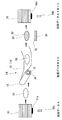
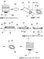
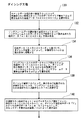
従来より、半導体ウエハを加工処理して、半導体を製造する方法としては、図19に示した工程によって行っている。
すなわち、図19の(A)に示したように、先ず、半導体ウエハ収納カセット201に収容された、表面に回路が形成された半導体ウエハ200を取り出して、その表面に、図示しない保護テープ貼着装置を介して、保護テープ202を貼着し、半導体ウエハ200の形状に沿って保護テープ202を切断する。
Conventionally, as a method of manufacturing a semiconductor by processing a semiconductor wafer, the process shown in FIG. 19 is performed.
That is, as shown in FIG. 19A, first, the
そして、保護テープ202が貼着された半導体ウエハ200を、半導体ウエハ収納カセット206に収容している(保護テープ貼着工程)。
次に、図19の(B)に示したように、半導体ウエハ収納カセット206から半導体ウエハ200を取り出して、保護テープ202が貼着された半導体ウエハ200に対して、保護テープ202側を、図示しない吸着テーブルに吸着保持して、回路が形成されていない裏面を、裏面研削装置(グラインダー)208によって、所定の厚さまで研削している。
Then, the semiconductor wafer 200 with the
Next, as shown in FIG. 19B, the
そして、所定の厚さまで裏面を研削した保護テープ202が貼着された半導体ウエハ200を、半導体ウエハ収納カセット210に収容している(裏面研削工程)。
その後、図19の(C)に示したように、半導体ウエハ収納カセット210から半導体ウエハ200を取り出して、保護テープ202側を、吸着テーブル212に吸着保持して、この半導体ウエハ200の外周に、リングフレーム214を載置する。
Then, the semiconductor wafer 200 to which the
After that, as shown in FIG. 19C, the
この状態で、上面からマウントテープ216を貼着して、リングフレーム214の外形状にマウントテープ216を切断することによって(または、リングフレーム214の形状に予めプリカットされたマウントテープ216を貼着することによって)、マウントテープ216を介して、半導体ウエハ200とリングフレーム214を一体化している。
In this state, the
そして、この半導体ウエハ200をリングフレームごと反転して、図示しない剥離テープを用いて、図19の(C)に示したように、半導体ウエハ200の回路面側の保護テープ202を剥離する。
Then, the
そして、保護テープ202が剥離され、マウントテープ216を介して、リングフレーム214と一体化された半導体ウエハ200を、半導体ウエハ収納カセット218に収容している(ウエハマウント工程)。
Then, the
次に、図19の(D)に示したように、半導体ウエハ収納カセット218から半導体ウエハ200をリングフレーム214ごと取り出して、ダイシング装置220によって、賽の目状に切断している。
Next, as shown in FIG. 19D, the
そして、ダイシング装置220によって、賽の目状に切断された半導体ウエハ200を、リングフレーム214ごと、半導体ウエハ収納カセット222に収容している(ダイシング工程)。
Then, the semiconductor wafer 200 that has been cut into a square shape by the
その後、図19の(E)に示したように、半導体ウエハ収納カセット222から半導体ウエハ200をリングフレーム214ごと取り出して、ボンディング装置224によって、賽の目状に切断された半導体ウエハ(チップ)200aをピックアップして、電子部品226の電子部品実装部に装着している(ダイボンディング工程)。
Thereafter, as shown in FIG. 19E, the
ところで、このような半導体製造方法において、工程管理、品質管理を行う方法として、従来より、バーコード法が採用されている。
すなわち、バーコード法では、ウエハの表面に刻印されているシリアルナンバーに対応したバーコードラベルを、半導体ウエハ収納カセットやリングフレームなどに貼着している。
By the way, in such a semiconductor manufacturing method, a barcode method has been conventionally employed as a method for performing process control and quality control.
That is, in the barcode method, a barcode label corresponding to the serial number stamped on the wafer surface is attached to a semiconductor wafer storage cassette, a ring frame, or the like.
そして、そのウエハに関する種々の情報を、このシリアルナンバーに対応させて、ホストコンピュータに登録している。
そして、半導体ウエハ製造方法のそれぞれの工程において、工程の管理に必要な情報を、シリアルナンバーに基づいて、ホストコンピュータから引き出し必要な処理を行うようになっている。
Various information about the wafer is registered in the host computer in correspondence with the serial number.
In each process of the semiconductor wafer manufacturing method, information necessary for process management is extracted from the host computer based on the serial number and necessary processing is performed.
しかしながら、このようなバーコード法では、情報を管理するホストコンピュータでウエハに関するすべての情報を管理する必要があり、ホストコンピュータの負担が大きくなってしまう。 However, in such a bar code method, it is necessary to manage all information related to the wafer by the host computer that manages the information, which increases the burden on the host computer.
また、通常は、ウエハの加工は一つの工場ですべての工程が行われるわけではなく、ある工場から他の工場へ移送されて加工が続けられる。ウエハに関する情報は、すべてホストコンピュータに登録されているため、ウエハが移送された工場において、新たにホストコンピュータにアクセスして必要な情報を引き出すか、または、ホストコンピュータに登録されている情報を、情報記録媒体に記憶させてウエハとともに移送し、移送先の工場のホストコンピュータに、再度ウエハに関する情報を登録する必要があり、工程管理が煩雑になってしまう。 In general, not all processes are performed in a single factory for wafer processing, but processing is continued by being transferred from one factory to another. Since all the information about the wafer is registered in the host computer, in the factory where the wafer is transferred, the host computer is newly accessed to extract necessary information, or the information registered in the host computer is It is necessary to store the information in the information recording medium and transfer it together with the wafer, and register the information about the wafer again in the host computer of the transfer destination factory, which complicates the process management.
このため、特許文献1(特開2000−331962号公報)では、電磁波を通信媒体として非接触で情報の入力、出力を行うことができるデータキャリアとして、例えば、ICチップと導電性コイルを接続して構成したいわゆるRFメモリーを、半導体ウエハを貼着支持する硬質板、リングフレームなどの半導体ウエハ支持部材上に固定することによって、必要な情報を読み書きして、データキャリアから読み取った情報によって、ウエハの加工を行う処理方法が提案されている。
しかしながら、この特許文献1に記載されたウエハの加工処理方法では、データキャリアが、半導体ウエハを貼着支持する硬質板、リングフレームなどの半導体ウエハ支持部材上に固定されているだけである。 However, in the wafer processing method described in Patent Document 1, the data carrier is only fixed on a semiconductor wafer support member such as a hard plate or a ring frame that adheres and supports the semiconductor wafer.
従って、例えば、図19の(A)の保護テープ貼着工程では、保護テープ202に関する情報については、保護テープ202の外装包装部材に貼着されたラベル、または、保護テープ202を巻装した軸芯部材に貼着されたラベルに記載された、例えば、バーコード、品名、品質保証期限、ロット番号などの情報を、別途、ホストコンピュータ228に登録する必要があり、工程管理が煩雑になってしまう。
Therefore, for example, in the protective tape sticking step of FIG. 19A, for information regarding the
しかも、保護テープ202を貼着する際には、例えば、個々の保護テープ202に応じた、貼着速度、貼着圧力などの最適条件などの、ホストコンピュータ228に登録された情報を引き出して、貼着工程を行わなければならず、工程管理が煩雑になってしまう。
Moreover, when sticking the
さらに、いったん保護テープ202を半導体ウエハ200に貼着した後には、この保護テープ202に関する情報は、次工程での加工処理を行う度に、ホストコンピュータ228に登録された情報を引き出して、加工工程を行わなければならず、工程管理が煩雑になってしまう。
Further, once the
また、いったん保護テープ202を半導体ウエハ200に貼着した後には、外見上、保護テープ202の種類などを判断するのは困難な場合があり、誤ってホストコンピュータ228に登録された情報を引き出してしまい、加工処理を行うおそれがあり、一定の品質の半導体が得られないおそれがある。
In addition, once the
また、最近では、多品種、小ロット生産が増加する傾向にあるが、この場合、一度使用した保護テープ202の残量、品質保証期限などの情報を得ることは困難であり、保護テープ202の残量不足、品質保証期限の超過などをきたすおそれがあり、工程中断や、品質の低下を招くおそれもある。
Recently, there is a tendency for the production of various types and small lots to increase. In this case, it is difficult to obtain information such as the remaining amount of the
このような問題は、図19の(C)に示したウエハマウント工程におけるマウントテープ216に関しても同様である。
本発明は、このような現状に鑑み、例えば、保護テープ、マウントテープなどの半導体ウエハ処理テープについて、そのテープ情報などの処理データを読み書きすることが可能なデータキャリア部材を備えた半導体ウエハ処理テープ巻装体を提供することを目的とする。
Such a problem also applies to the
In view of such a current situation, the present invention provides a semiconductor wafer processing tape provided with a data carrier member capable of reading and writing processing data such as tape information on a semiconductor wafer processing tape such as a protective tape and a mount tape. An object is to provide a wound body.
また、本発明は、このような半導体ウエハ処理テープ巻装体を用いることによって、従来のようにホストコンピュータにアクセスすることなく、データキャリア部材に書き込まれた処理データを読み取り、読み取られた処理データに基づいて、半導体ウエハ処理テープを、最適条件で、半導体ウエハに貼着することが可能な半導体ウエハ処理テープ貼着装置を提供することを目的とする。 Further, the present invention uses such a semiconductor wafer processing tape winding body to read processing data written on the data carrier member without accessing the host computer as in the prior art, and to read the processing data read It is an object of the present invention to provide a semiconductor wafer processing tape sticking apparatus capable of sticking a semiconductor wafer processing tape to a semiconductor wafer under optimum conditions.
また、本発明は、このような半導体ウエハ処理テープ貼着装置によって、半導体ウエハ処理テープが貼着された半導体ウエハに対して、最適条件で、所定のウエハ加工処理を行うことが可能な半導体ウエハ加工処理装置、特に、半導体ウエハ研削装置、ダイシング装置、およびダイボンディング装置を提供することを目的とする。 The present invention also provides a semiconductor wafer that can be subjected to a predetermined wafer processing process under optimum conditions for a semiconductor wafer to which a semiconductor wafer processing tape is attached by using such a semiconductor wafer processing tape attaching apparatus. An object of the present invention is to provide a processing apparatus, in particular, a semiconductor wafer grinding apparatus, a dicing apparatus, and a die bonding apparatus.
本発明は、前述したような従来技術における課題及び目的を達成するために発明されたものであって、本発明の半導体ウエハ処理テープ巻装体は、
半導体ウエハに貼着することよって、半導体ウエハの加工を行うための半導体ウエハ処理テープと、
前記半導体ウエハ処理テープを巻装した軸芯部材と、
前記軸芯部材に備えられ、所望の処理データを読み書き可能なデータキャリア部材と、を備えることを特徴とする。
The present invention was invented in order to achieve the above-described problems and objects in the prior art, and the semiconductor wafer processing tape winding body of the present invention comprises:
A semiconductor wafer processing tape for processing a semiconductor wafer by sticking to the semiconductor wafer;
An axial core member wound with the semiconductor wafer processing tape;
A data carrier member provided on the shaft core member and capable of reading and writing desired processing data.
このように構成することによって、例えば、品名、品質保証期限、テープ長さ、テープ幅、ロット番号、半導体ウエハに最適な貼着圧力、貼着速度などの情報を、軸芯部材に備えられたデータキャリア部材に書き込むことができる。 By configuring in this way, for example, the shaft core member is provided with information such as product name, quality assurance deadline, tape length, tape width, lot number, adhesion pressure optimum for the semiconductor wafer, and adhesion speed. The data carrier member can be written.
これにより、半導体ウエハにこの半導体ウエハ処理テープ巻装体に巻装された半導体ウエハ処理テープを貼着して半導体ウエハの加工を行う際に、従来のようにホストコンピュータにアクセスすることなく、データキャリア部材に書き込まれた処理データを読み取り、読み取られた処理データに基づいて、半導体ウエハ処理テープを、最適条件で、半導体ウエハに貼着することが可能である。 As a result, when a semiconductor wafer is processed by attaching the semiconductor wafer processing tape wound around the semiconductor wafer processing tape winding body to the semiconductor wafer, the data is accessed without accessing the host computer as in the prior art. The processing data written on the carrier member can be read, and the semiconductor wafer processing tape can be attached to the semiconductor wafer under optimum conditions based on the read processing data.
従って、別途、ホストコンピュータに、このような半導体ウエハ処理テープの情報を登録する必要がなく、また、加工の際にも、ホストコンピュータに登録された情報を引き出す必要もなく、各種のウエハ加工工程を行え、工程管理が簡単になる。 Therefore, it is not necessary to separately register such semiconductor wafer processing tape information in the host computer, and it is not necessary to extract information registered in the host computer during processing, and various wafer processing steps Process management.
しかも、一度使用した半導体ウエハ処理テープの残量、品質保証期限などの情報を、軸芯部材に備えられたデータキャリア部材に書き込み、ウエハ加工の際にこれらの情報を読み取ることによって、半導体ウエハ処理テープの残量不足、品質保証期限の超過などをきたすおそれがなく、工程中断や、品質の低下を招くおそれもない。 Moreover, by writing information such as the remaining amount of semiconductor wafer processing tape once used and the quality assurance deadline to the data carrier member provided on the shaft core member, and reading this information during wafer processing, the semiconductor wafer processing There is no risk of a shortage of tape remaining, an expiration date for quality assurance, etc., and there is no risk of process interruption or quality degradation.
また、本発明の半導体ウエハ処理テープ巻装体は、前記データキャリア部材が、非接触型のデータキャリア部材であることを特徴とする。
また、本発明の半導体ウエハ処理テープ巻装体は、前記非接触型のデータキャリア部材が、ICチップと、このICチップに接続された導電性コイルとから構成されるRFメモリーであることを特徴とする。
In the semiconductor wafer processing tape winding body of the present invention, the data carrier member is a non-contact type data carrier member.
In the semiconductor wafer processing tape winding body of the present invention, the non-contact type data carrier member is an RF memory including an IC chip and a conductive coil connected to the IC chip. And
このように、軸芯部材に備えられたデータキャリア部材が、非接触型のデータキャリア部材、特に、ICチップと、このICチップに接続された導電性コイルとから構成されるRFメモリーとすることによって、上記の半導体ウエハ処理テープの情報の書き込み、読み取りが瞬時にしかも確実に行え、工程を短縮化できるとともに、正確なウエハ加工処理を行え、半導体製品の品質が低下することがない。 Thus, the data carrier member provided in the shaft core member is a non-contact type data carrier member, in particular, an RF memory including an IC chip and a conductive coil connected to the IC chip. Thus, writing and reading of information on the semiconductor wafer processing tape can be performed instantaneously and reliably, the process can be shortened, and accurate wafer processing can be performed, so that the quality of the semiconductor product does not deteriorate.
また、本発明の半導体ウエハ処理テープ巻装体は、前記データキャリア部材が、軸芯部材の表面に設けられていることを特徴とする。
このようにデータキャリア部材が、軸芯部材の表面に設けられているので、上記の半導体ウエハ処理テープの情報の書き込み、読み取りが瞬時にしかも確実に行え、工程を短縮化できるとともに、正確なウエハ加工処理を行え、半導体製品の品質が低下することがない。
Moreover, the semiconductor wafer processing tape winding body of the present invention is characterized in that the data carrier member is provided on the surface of the shaft member.
As described above, since the data carrier member is provided on the surface of the shaft core member, writing and reading of information on the semiconductor wafer processing tape can be instantaneously and reliably performed, the process can be shortened, and an accurate wafer can be obtained. Processing can be performed and the quality of the semiconductor product does not deteriorate.
また、本発明の半導体ウエハ処理テープ巻装体は、前記データキャリア部材が、軸芯部材に埋設状態で設けられていることを特徴とする。
このようにデータキャリア部材が、軸芯部材に埋設状態で設けられているので、軸芯部材に半導体ウエハ処理テープを巻装する際に、データキャリア部材が邪魔にならず、半導体ウエハ処理テープの巻きむらが発生することがなく、データキャリア部材が破損損傷するおそれもない。
In the semiconductor wafer processing tape winding body of the present invention, the data carrier member is provided in an embedded state in the shaft core member.
As described above, since the data carrier member is embedded in the shaft core member, when the semiconductor wafer processing tape is wound around the shaft core member, the data carrier member does not get in the way, and the semiconductor wafer processing tape No winding unevenness occurs, and there is no possibility that the data carrier member is damaged or damaged.
しかも、軸芯部材を巻き出し装置の巻き出し軸に脱着する際にも、脱着作業の邪魔にならず、データキャリア部材が破損損傷するおそれもない。
また、本発明の半導体ウエハ処理テープ巻装体は、前記データキャリア部材が、軸芯部材の内径側に設けられていることを特徴とする。
Moreover, when the shaft core member is attached to and detached from the unwinding shaft of the unwinding device, it does not interfere with the attaching / detaching operation, and the data carrier member is not damaged or damaged.
Moreover, the semiconductor wafer processing tape winding body of the present invention is characterized in that the data carrier member is provided on the inner diameter side of the shaft core member.
このようにデータキャリア部材が、軸芯部材の内径側に設けられているので、軸芯部材に半導体ウエハ処理テープを巻装する際に、データキャリア部材が邪魔にならず、半導体ウエハ処理テープの巻きむらが発生することがなく、データキャリア部材が破損損傷するおそれもない。 Thus, since the data carrier member is provided on the inner diameter side of the shaft core member, when the semiconductor wafer processing tape is wound around the shaft core member, the data carrier member does not get in the way, and the semiconductor wafer processing tape No winding unevenness occurs, and there is no possibility that the data carrier member is damaged or damaged.
しかも、例えば、軸芯部材を巻き出し装置の巻き出し軸に脱着する際に、巻き出し軸側に読み書き装置を設けておけば、このデータキャリア部材の情報を読み書きすることができ、一度使用した半導体ウエハ処理テープの残量、品質保証期限などの情報を、軸芯部材に備えられたデータキャリア部材に書き込み、ウエハ加工の際にこれらの情報を読み取ることによって、半導体ウエハ処理テープの残量不足、品質保証期限の超過などをきたすおそれがなく、工程中断や、品質の低下を招くおそれもない。 Moreover, for example, when the shaft core member is attached to and detached from the unwinding shaft of the unwinding device, if a read / write device is provided on the unwinding shaft side, the information on the data carrier member can be read and written and used once. Information on the remaining amount of semiconductor wafer processing tape, quality assurance deadline, etc. is written on the data carrier member provided on the shaft core member, and the remaining information on the semiconductor wafer processing tape is insufficient by reading this information during wafer processing. In addition, there is no possibility that the quality guarantee period will be exceeded, and there is no possibility that the process will be interrupted or the quality will be deteriorated.
また、本発明の半導体ウエハ処理テープ巻装体は、前記データキャリア部材が、軸芯部材の外径側に設けられていることを特徴とする。
このようにデータキャリア部材が、軸芯部材の外径側に設けられているので、軸芯部材の材質によっても、電磁波が遮断されることがなく、上記の半導体ウエハ処理テープの情報の書き込み、読み取りが瞬時にしかも確実に行え、工程を短縮化できるとともに、正確なウエハ加工処理を行え、半導体製品の品質が低下することがない。
In the semiconductor wafer processing tape winding body of the present invention, the data carrier member is provided on the outer diameter side of the shaft core member.
As described above, since the data carrier member is provided on the outer diameter side of the shaft core member, the electromagnetic wave is not blocked by the material of the shaft core member. Reading can be performed instantly and reliably, the process can be shortened, accurate wafer processing can be performed, and the quality of the semiconductor product does not deteriorate.
また、本発明の半導体ウエハ処理テープ貼着装置は、
上記のいずれかに記載の半導体ウエハ処理テープ巻装体を、脱着自在に装着可能な巻き出し軸を備えた巻き出し装置と、
前記半導体ウエハ処理テープ巻装体のデータキャリア部材に書き込まれた処理データを読み書きするテープデータ読み書き装置と、
前記テープデータ読み書き装置によって読み取られた処理データに基づいて、巻き出し装置から巻き出された半導体ウエハ処理テープを、半導体ウエハに貼着するテープ貼着装置とを備えることを特徴とする。
Moreover, the semiconductor wafer processing tape sticking apparatus of the present invention is
The semiconductor wafer processing tape winding body according to any one of the above, an unwinding device equipped with an unwinding shaft that can be detachably mounted;
A tape data read / write device for reading / writing process data written on a data carrier member of the semiconductor wafer processing tape winding body;
And a tape adhering device for adhering the semiconductor wafer processing tape unwound from the unwinding device to the semiconductor wafer based on the processing data read by the tape data read / write device.
このように構成することによって、半導体ウエハ処理テープ巻装体の軸芯部材に備えられたデータキャリア部材に書き込まれた、例えば、品名、品質保証期限、テープ長さ、テープ幅、ロット番号、半導体ウエハに最適な貼着圧力、貼着速度などの情報を、テープデータ読み書き装置によって読み取ることができる。 By configuring in this way, for example, product name, quality assurance period, tape length, tape width, lot number, semiconductor written in the data carrier member provided in the shaft core member of the semiconductor wafer processing tape winding body Information such as the optimum adhesion pressure and adhesion speed for the wafer can be read by a tape data read / write device.
そして、このテープデータ読み書き装置によって読み取られた処理データに基づいて、テープ貼着装置によって、巻き出し装置から巻き出された半導体ウエハ処理テープを、半導体ウエハに貼着することができる。 Based on the processing data read by the tape data read / write device, the semiconductor wafer processing tape unwound from the unwinding device can be stuck to the semiconductor wafer by the tape sticking device.
従って、従来のようにホストコンピュータにアクセスすることなく、テープデータ読み書き装置によって、データキャリア部材に書き込まれた処理データを読み取り、読み取られた処理データに基づいて、半導体ウエハ処理テープを、最適条件で、半導体ウエハに貼着することが可能である。 Therefore, the processing data written on the data carrier member is read by the tape data read / write device without accessing the host computer as in the prior art, and the semiconductor wafer processing tape is loaded under the optimum conditions based on the read processing data. It can be attached to a semiconductor wafer.
従って、別途、ホストコンピュータに、このような半導体ウエハ処理テープの情報を登録する必要がなく、また、加工の際にも、ホストコンピュータに登録された情報を引き出す必要もなく、各種のウエハ加工工程を行え、工程管理が簡単になる。 Therefore, it is not necessary to separately register such semiconductor wafer processing tape information in the host computer, and it is not necessary to extract information registered in the host computer during processing, and various wafer processing steps Process management.
しかも、一度使用した半導体ウエハ処理テープの残量、品質保証期限などの情報を、軸芯部材に備えられたデータキャリア部材に、テープデータ読み書き装置によって、書き込み、ウエハ加工の際にこれらの情報を読み取ることによって、半導体ウエハ処理テープの残量不足、品質保証期限の超過などをきたすおそれがなく、工程中断や、品質の低下を招くおそれもない。 In addition, information such as the remaining amount of semiconductor wafer processing tape that has been used once, the quality assurance deadline, etc. are written to the data carrier member provided on the shaft core member by a tape data read / write device, and this information is stored during wafer processing. By reading, there is no possibility that the remaining amount of the semiconductor wafer processing tape will be insufficient, the quality guarantee period will not be exceeded, etc., and there is no possibility that the process will be interrupted or the quality will be deteriorated.
また、本発明の半導体ウエハ処理テープ貼着装置は、前記テープデータ読み書き装置が、巻き出し軸に設けられていることを特徴とする。
このように構成することによって、半導体ウエハ処理テープ巻装体を巻き出し装置の巻き出し軸に装着するだけで、半導体ウエハ処理テープ巻装体の軸芯部材に備えられたデータキャリア部材に書き込まれた、例えば、品名、品質保証期限、テープ長さ、テープ幅、ロット番号、半導体ウエハに最適な貼着圧力、貼着速度などの情報を、テープデータ読み書き装置によって、迅速にかつ確実に読み取ることができる。
Moreover, the semiconductor wafer processing tape sticking apparatus of the present invention is characterized in that the tape data read / write device is provided on an unwinding shaft.
With this configuration, the semiconductor wafer processing tape winding body can be written on the data carrier member provided on the shaft core member of the semiconductor wafer processing tape winding body simply by mounting the semiconductor wafer processing tape winding body on the unwinding shaft of the unwinding apparatus. In addition, for example, information such as product name, quality assurance deadline, tape length, tape width, lot number, optimum adhesion pressure and adhesion speed for semiconductor wafers can be read quickly and reliably using a tape data reader / writer. Can do.
しかも、一度使用した半導体ウエハ処理テープの残量、品質保証期限などの情報を、軸芯部材に備えられたデータキャリア部材に、テープデータ読み書き装置によって、迅速にかつ確実に書き込み、半導体ウエハ処理テープ巻装体を巻き出し装置の巻き出し軸から取り外すことができる。 Moreover, information such as the remaining amount of semiconductor wafer processing tape once used and the quality guarantee deadline can be quickly and surely written to the data carrier member provided on the shaft core member by a tape data read / write device. The wound body can be removed from the unwinding shaft of the unwinding device.
また、本発明の半導体ウエハ処理テープ貼着装置は、
前記テープ貼着装置によって半導体ウエハ処理テープが貼着された半導体ウエハを収納する半導体ウエハ収納カセットに対して、
前記半導体ウエハ収納カセットに設けられたデータキャリア部材に、所望の処理データを書き込むカセットデータ書き込み装置を備えることを特徴とする。
Moreover, the semiconductor wafer processing tape sticking apparatus of the present invention is
For a semiconductor wafer storage cassette for storing a semiconductor wafer to which a semiconductor wafer processing tape is attached by the tape attaching device,
A cassette data writing device for writing desired processing data on a data carrier member provided in the semiconductor wafer storage cassette is provided.
このように構成することによって、カセットデータ書き込み装置によって、テープ貼着装置によって半導体ウエハ処理テープを貼着した際の様々な情報、例えば、半導体ウエハ処理テープの品名、品質保証期限、ロット番号、貼着圧力、貼着速度、半導体ウエハの種類、厚さなどの情報を、半導体ウエハ収納カセットに設けられたデータキャリア部材に書き込むことができる。 With this configuration, various information when the semiconductor wafer processing tape is stuck by the tape sticking device by the cassette data writing device, for example, the product name, quality guarantee date, lot number, sticking of the semiconductor wafer processing tape, etc. Information such as adhesion pressure, adhesion speed, semiconductor wafer type, and thickness can be written on a data carrier member provided in the semiconductor wafer storage cassette.
従って、次工程で、半導体ウエハを加工処理する際に、従来のようにホストコンピュータにアクセスすることなく、半導体ウエハ収納カセットに設けられたデータキャリア部材に書き込まれた処理データを読み取り、読み取られた処理データに基づいて、半導体ウエハを、最適条件で、加工処理することが可能である。 Therefore, when processing the semiconductor wafer in the next step, the processing data written on the data carrier member provided in the semiconductor wafer storage cassette is read and read without accessing the host computer as in the prior art. Based on the processing data, the semiconductor wafer can be processed under optimum conditions.
また、本発明の半導体ウエハ処理テープ貼着装置は、前記半導体ウエハ処理テープ貼着装置が、半導体ウエハの回路面を保護するための保護テープを貼着する保護テープ貼着装置であることを特徴とする。 Moreover, the semiconductor wafer processing tape sticking apparatus of the present invention is a protective tape sticking apparatus for sticking a protective tape for protecting the circuit surface of the semiconductor wafer. And
このように構成することによって、半導体ウエハ処理テープ巻装体のデータキャリア部材に書き込まれた処理データを、テープデータ読み書き装置によって読み取り、この処理データに基づいて、保護テープ貼着装置によって、半導体ウエハの回路面を保護するための保護テープを、最適条件で半導体ウエハの回路面に貼着することができる。 By comprising in this way, the processing data written in the data carrier member of the semiconductor wafer processing tape winding body are read by the tape data read / write device, and based on this processing data, the semiconductor wafer is processed by the protective tape attaching device. A protective tape for protecting the circuit surface can be adhered to the circuit surface of the semiconductor wafer under optimum conditions.
また、本発明の半導体ウエハ処理テープ貼着装置は、前記半導体ウエハ処理テープ貼着装置が、半導体ウエハの外周にリングフレームを貼着するマウントテープを貼着するマウントテープ貼着装置であることを特徴とする。 Moreover, the semiconductor wafer processing tape sticking device of the present invention is a mounting tape sticking device for sticking a mount tape for sticking a ring frame to the outer periphery of the semiconductor wafer. Features.
このように構成することによって、半導体ウエハ処理テープ巻装体のデータキャリア部材に書き込まれた処理データを、テープデータ読み書き装置によって読み取り、この処理データに基づいて、半導体ウエハの外周にリングフレームを、マウントテープを介して、最適条件で半導体ウエハの外周に貼着することができる。 By configuring in this way, processing data written on the data carrier member of the semiconductor wafer processing tape winding body is read by a tape data read / write device, and based on this processing data, a ring frame is formed on the outer periphery of the semiconductor wafer, It can be attached to the outer periphery of a semiconductor wafer under optimum conditions via a mounting tape.
また、本発明の半導体ウエハ処理テープ貼着装置は、前記リングフレームに設けられたデータキャリア部材に、所望の処理データを書き込むリングフレームデータ書き込み装置を備えることを特徴とする。 Moreover, the semiconductor wafer processing tape sticking apparatus of the present invention includes a ring frame data writing device for writing desired processing data on a data carrier member provided on the ring frame.
このように構成することによって、リングフレームデータ書き込み装置によって、テープ貼着装置によって半導体ウエハ処理テープを貼着した際の様々な情報、例えば、半導体ウエハ処理テープの品名、品質保証期限、ロット番号、貼着圧力、貼着速度、半導体ウエハの種類、厚さなどの情報を、リングフレームに設けられたデータキャリア部材に書き込むことができる。 By configuring in this way, various information when the semiconductor wafer processing tape is stuck by the tape sticking device by the ring frame data writing device, for example, the product name of the semiconductor wafer processing tape, the quality guarantee period, the lot number, Information such as sticking pressure, sticking speed, semiconductor wafer type, and thickness can be written on a data carrier member provided on the ring frame.
従って、次工程で、半導体ウエハを加工処理する際に、従来のようにホストコンピュータにアクセスすることなく、リングフレームに設けられたデータキャリア部材に書き込まれた処理データを読み取り、読み取られた処理データに基づいて、半導体ウエハを、半導体ウエハ一枚ごとに、最適条件で、加工処理することが可能である。 Therefore, when processing the semiconductor wafer in the next step, the processing data written on the data carrier member provided in the ring frame is read without accessing the host computer as in the prior art, and the read processing data Based on the above, it is possible to process the semiconductor wafer for each semiconductor wafer under optimum conditions.
また、本発明の半導体ウエハ処理テープ貼着装置は、
前記半導体ウエハ処理テープ貼着装置が、
前工程で所定の加工処理が行われた半導体ウエハを収納する、半導体ウエハ収納カセットに設けられたデータキャリア部材に書き込まれた処理データを読み取る、カセットデータ読み取り装置を備え、
前記カセットデータ読み取り装置で読み取られた処理データと、前記テープデータ読み書き装置によって読み取られた処理データに基づいて、テープ貼着装置によって、半導体ウエハ処理テープを、半導体ウエハに貼着するように構成されていることを特徴とする。
Moreover, the semiconductor wafer processing tape sticking apparatus of the present invention is
The semiconductor wafer processing tape sticking device is
A cassette data reader is provided for storing the semiconductor wafer that has been subjected to the predetermined processing in the previous process, and for reading the processing data written on the data carrier member provided in the semiconductor wafer storage cassette.
Based on the processing data read by the cassette data reader and the processing data read by the tape data read / write device, the semiconductor wafer processing tape is attached to the semiconductor wafer by the tape attaching device. It is characterized by.
このように構成することによって、カセットデータ読み取り装置によって、前工程のウエハ加工工程における処理データ、例えば、半導体ウエハ処理テープの品名、品質保証期限、ロット番号、貼着圧力、貼着速度、半導体ウエハの種類、厚さ、前工程における加工条件などの処理データを、半導体ウエハ収納カセットに設けられたデータキャリア部材から読み取ることができる。 By configuring in this way, the processing data in the wafer processing step of the previous step, for example, the product name of the semiconductor wafer processing tape, the quality guarantee deadline, the lot number, the adhering pressure, the adhering speed, the semiconductor wafer by the cassette data reader The processing data such as the type, thickness, and processing conditions in the previous process can be read from the data carrier member provided in the semiconductor wafer storage cassette.
一方、半導体ウエハ処理テープ巻装体の軸芯部材に備えられたデータキャリア部材に書き込まれた、例えば、品名、品質保証期限、テープ長さ、テープ幅、ロット番号、半導体ウエハに最適な貼着圧力、貼着速度などの情報を、テープデータ読み書き装置によって読み取ることができる。 On the other hand, for example, product name, quality assurance period, tape length, tape width, lot number, and optimum adhesion to the semiconductor wafer written on the data carrier member provided on the shaft core member of the semiconductor wafer processing tape winding body Information such as pressure and sticking speed can be read by a tape data read / write device.
そして、従来のようにホストコンピュータにアクセスすることなく、これらの処理データに基づいて、半導体ウエハ処理テープを、最適条件で、半導体ウエハに貼着することができる。 Then, the semiconductor wafer processing tape can be attached to the semiconductor wafer under the optimum conditions based on these processing data without accessing the host computer as in the prior art.
また、本発明の半導体ウエハ加工処理装置は、
上記のいずれかに記載の半導体ウエハ処理テープ貼着装置によって、半導体ウエハ処理テープが貼着された半導体ウエハに対して、
前記テープ貼着装置によって半導体ウエハ処理テープが貼着された半導体ウエハを収納する、半導体ウエハ収納カセットに設けられたデータキャリア部材に書き込まれた処理データに基づいて、所定のウエハ加工処理を行うように構成したことを特徴とする。
Further, the semiconductor wafer processing apparatus of the present invention is
By the semiconductor wafer processing tape sticking apparatus according to any of the above, for the semiconductor wafer to which the semiconductor wafer processing tape is stuck,
A predetermined wafer processing process is performed based on processing data written in a data carrier member provided in a semiconductor wafer storage cassette for storing a semiconductor wafer having a semiconductor wafer processing tape attached thereto by the tape attaching device. It is characterized by comprising.
このように構成することによって、テープ貼着装置によって半導体ウエハ処理テープを貼着した際の様々な情報、例えば、半導体ウエハ処理テープの品名、品質保証期限、ロット番号、貼着圧力、貼着速度、半導体ウエハの種類、厚さなどの情報を、次工程で、半導体ウエハを加工処理する際に、従来のようにホストコンピュータにアクセスすることなく、半導体ウエハ収納カセットに設けられたデータキャリア部材に書き込まれた処理データを読み取り、読み取られた処理データに基づいて、半導体ウエハを、最適条件で、加工処理することが可能である。 By configuring in this way, various information when the semiconductor wafer processing tape is stuck by the tape sticking device, for example, the product name, quality guarantee date, lot number, sticking pressure, sticking speed of the semiconductor wafer processing tape When processing a semiconductor wafer in the next process, information such as the type and thickness of the semiconductor wafer is stored in the data carrier member provided in the semiconductor wafer storage cassette without accessing the host computer as in the prior art. It is possible to read the written processing data and process the semiconductor wafer under optimum conditions based on the read processing data.
また、本発明の半導体ウエハ加工処理装置は、
上記のいずれかに記載の半導体ウエハ処理テープ貼着装置によって、半導体ウエハ処理テープが貼着された半導体ウエハに対して、
前記リングフレームに設けられたデータキャリア部材に書き込まれた処理データに基づいて、所定のウエハ加工処理を行うように構成したことを特徴とする。
Further, the semiconductor wafer processing apparatus of the present invention is
By the semiconductor wafer processing tape sticking apparatus according to any of the above, for the semiconductor wafer to which the semiconductor wafer processing tape is stuck,
A predetermined wafer processing is performed based on processing data written on a data carrier member provided in the ring frame.
このように構成することによって、テープ貼着装置によって半導体ウエハ処理テープを貼着した際の様々な情報、例えば、半導体ウエハ処理テープの品名、品質保証期限、ロット番号、貼着圧力、貼着速度、半導体ウエハの種類、厚さなどの情報を、次工程で、半導体ウエハを加工処理する際に、従来のようにホストコンピュータにアクセスすることなく、リングフレームに設けられたデータキャリア部材に書き込まれた処理データを読み取り、読み取られた処理データに基づいて、半導体ウエハを、半導体ウエハ一枚ごとに、最適条件で、加工処理することが可能である。 By configuring in this way, various information when the semiconductor wafer processing tape is stuck by the tape sticking device, for example, the product name, quality guarantee date, lot number, sticking pressure, sticking speed of the semiconductor wafer processing tape When processing a semiconductor wafer in the next process, information such as the type and thickness of the semiconductor wafer is written to a data carrier member provided on the ring frame without accessing the host computer as in the prior art. It is possible to read the processed data and process the semiconductor wafer under the optimum conditions for each semiconductor wafer based on the read processed data.
また、本発明の半導体ウエハ加工処理装置は、前記半導体ウエハ加工処理装置が、半導体ウエハの回路面と反対側の裏面を研削する半導体ウエハ研削装置であることを特徴とする。 The semiconductor wafer processing apparatus according to the present invention is characterized in that the semiconductor wafer processing apparatus is a semiconductor wafer grinding apparatus for grinding a back surface opposite to a circuit surface of the semiconductor wafer.
このように構成することによって、例えば、半導体ウエハ処理テープである回路面を保護する保護テープの品名、品質保証期限、ロット番号、貼着圧力、貼着速度、半導体ウエハの種類、厚さなどの情報を、半導体ウエハの回路面と反対側の裏面を研削する際に、従来のようにホストコンピュータにアクセスすることなく、半導体ウエハ収納カセットに設けられたデータキャリア部材に書き込まれた処理データを読み取り、読み取られた処理データに基づいて、半導体ウエハ研削装置によって、最適条件で、裏面研削処理することが可能である。 By configuring in this way, for example, the name of the protective tape that protects the circuit surface, which is a semiconductor wafer processing tape, quality assurance deadline, lot number, sticking pressure, sticking speed, semiconductor wafer type, thickness, etc. When grinding the back surface of the semiconductor wafer opposite to the circuit surface of the semiconductor wafer, the processing data written in the data carrier member provided in the semiconductor wafer storage cassette is read without accessing the host computer as in the past. Based on the read processing data, the back surface grinding process can be performed under the optimum conditions by the semiconductor wafer grinding apparatus.
また、本発明の半導体ウエハ加工処理装置は、前記半導体ウエハ加工処理装置が、半導体ウエハを賽の目状に切断するダイシング装置であることを特徴とする。
このように構成することによって、例えば、半導体ウエハ処理テープである半導体ウエハの外周にリングフレームを貼着するマウントテープの品名、品質保証期限、ロット番号、貼着圧力、貼着速度、半導体ウエハの種類、厚さなどの情報を、半導体ウエハを賽の目状に切断する際に、従来のようにホストコンピュータにアクセスすることなく、半導体ウエハ収納カセットに設けられたデータキャリア部材に書き込まれた処理データを読み取り、読み取られた処理データに基づいて、ダイシング装置によって、最適条件で、半導体ウエハを賽の目状に切断することが可能である。
Moreover, the semiconductor wafer processing apparatus of the present invention is characterized in that the semiconductor wafer processing apparatus is a dicing apparatus that cuts the semiconductor wafer into a square shape.
By configuring in this way, for example, the product name of the mounting tape that attaches the ring frame to the outer periphery of the semiconductor wafer, which is a semiconductor wafer processing tape, the quality assurance period, the lot number, the attaching pressure, the attaching speed, the semiconductor wafer Processing data written on the data carrier member provided in the semiconductor wafer storage cassette without accessing the host computer as in the past when cutting information such as type and thickness into the shape of a ridge. Based on the read processing data, it is possible to cut the semiconductor wafer into a square shape under the optimum conditions by the dicing apparatus.
また、本発明の半導体ウエハ加工処理装置は、前記半導体ウエハ加工処理装置が、賽の目状に切断された半導体チップをピックアップして、電子部品の電子部品実装部に装着するダイボンディング装置であることを特徴とする。 Further, the semiconductor wafer processing apparatus of the present invention is a die bonding apparatus in which the semiconductor wafer processing apparatus picks up a semiconductor chip cut into a grid shape and mounts it on an electronic component mounting portion of the electronic component. Features.
このように構成することによって、例えば、半導体ウエハ処理テープである半導体ウエハの外周にリングフレームを貼着するマウントテープの品名、品質保証期限、ロット番号、貼着圧力、貼着速度、半導体ウエハの種類、厚さなどの情報を、賽の目状に切断された半導体チップをピックアップして、電子部品の電子部品実装部に装着する際に、従来のようにホストコンピュータにアクセスすることなく、半導体ウエハ収納カセットに設けられたデータキャリア部材に書き込まれた処理データを読み取り、読み取られた処理データに基づいて、ダイボンディング装置によって、最適条件で、賽の目状に切断された半導体チップをピックアップして、電子部品の電子部品実装部に装着することが可能である。 By configuring in this way, for example, the product name of the mounting tape that attaches the ring frame to the outer periphery of the semiconductor wafer, which is a semiconductor wafer processing tape, the quality assurance deadline, the lot number, the attaching pressure, the attaching speed, the semiconductor wafer The semiconductor wafer can be stored without accessing the host computer as in the past when picking up the semiconductor chip cut in the shape of a ridge and mounting it on the electronic component mounting part of the electronic component, such as the type and thickness. The processing data written on the data carrier member provided in the cassette is read. Based on the processing data thus read, the die bonding device picks up the semiconductor chip cut in the shape of a scissors under the optimum conditions, and the electronic component. It can be mounted on the electronic component mounting part.
本発明によれば、例えば、品名、品質保証期限、テープ長さ、テープ幅、ロット番号、半導体ウエハに最適な貼着圧力、貼着速度などの情報を、軸芯部材に備えられたデータキャリア部材に書き込むことができる。 According to the present invention, for example, the data carrier provided with the shaft core member includes information such as the product name, quality assurance period, tape length, tape width, lot number, and the optimum adhesion pressure and adhesion speed for the semiconductor wafer. The member can be written.
これにより、半導体ウエハにこの半導体ウエハ処理テープ巻装体に巻装された半導体ウエハ処理テープを貼着して半導体ウエハの加工を行う際に、従来のようにホストコンピュータにアクセスすることなく、データキャリア部材に書き込まれた処理データを読み取り、読み取られた処理データに基づいて、半導体ウエハ処理テープを、最適条件で、半導体ウエハに貼着することが可能である。 As a result, when a semiconductor wafer is processed by attaching the semiconductor wafer processing tape wound around the semiconductor wafer processing tape winding body to the semiconductor wafer, the data is accessed without accessing the host computer as in the prior art. The processing data written on the carrier member can be read, and the semiconductor wafer processing tape can be attached to the semiconductor wafer under optimum conditions based on the read processing data.
従って、別途、ホストコンピュータに、このような半導体ウエハ処理テープの情報を登録する必要がなく、また、加工の際にも、ホストコンピュータに登録された情報を引き出す必要もなく、各種のウエハ加工工程を行え、工程管理が簡単になる。 Therefore, it is not necessary to separately register such semiconductor wafer processing tape information in the host computer, and it is not necessary to extract information registered in the host computer during processing, and various wafer processing steps Process management.
しかも、一度使用した半導体ウエハ処理テープの残量、品質保証期限などの情報を、軸芯部材に備えられたデータキャリア部材に書き込み、ウエハ加工の際にこれらの情報を読み取ることによって、半導体ウエハ処理テープの残量不足、品質保証期限の超過などをきたすおそれがなく、工程中断や、品質の低下を招くおそれもない。 Moreover, by writing information such as the remaining amount of semiconductor wafer processing tape once used and the quality assurance deadline to the data carrier member provided on the shaft core member, and reading this information during wafer processing, the semiconductor wafer processing There is no risk of a shortage of tape remaining, an expiration date for quality assurance, etc., and there is no risk of process interruption or quality degradation.
以下、本発明の実施の形態(実施例)を図面に基づいてより詳細に説明する。
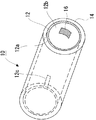
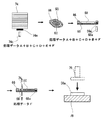
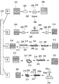
図1は、本発明の半導体ウエハ処理テープ巻装体の実施例の概略斜視図である。
図1において、10は、全体で本発明の半導体ウエハ処理テープ巻装体を示している。
Hereinafter, embodiments (examples) of the present invention will be described in more detail with reference to the drawings.
FIG. 1 is a schematic perspective view of an embodiment of a semiconductor wafer processing tape winding body of the present invention.
In FIG. 1,
図1に示したように、半導体ウエハ処理テープ巻装体10は、略円筒形状の軸芯部材12を備えており、この軸芯部材12の外径側の表面12aに、半導体ウエハ処理テープ14が巻装されている。
As shown in FIG. 1, the semiconductor wafer processing
この半導体ウエハ処理テープ14は、半導体ウエハに貼着することによって、半導体ウエハの種々の加工を行うためのものであって、例えば、半導体ウエハの裏面を研削する際に、半導体ウエハの回路面を保護するための保護テープ、半導体ウエハの外周にリングフレームを貼着するマウントテープ、その他、種々の半導体ウエハ加工を行う際に使用されるものであって特に限定されるものではない。
The semiconductor
このような半導体ウエハ処理テープ14としては、例えば、特開昭60−196956号公報、特開昭60−223139号公報、特開平5−32946号公報、特開平8−27239号公報等に記載されているように、基材の表面に、例えば、アクリル系エネルギー線硬化型粘着剤などのエネルギー線硬化型粘着剤を形成したものなどが使用可能である。
Such a semiconductor
また、軸芯部材12としては、その材質は特に限定されるものではなく、例えば、ポリエチレン樹脂、ポリプロピレン樹脂、ABS樹脂などの合成樹脂などが使用可能である。
そして、この実施例の半導体ウエハ処理テープ巻装体10では、軸芯部材12の内径側の表面12bの一端に、データキャリア部材16が設けられている。
The material of the
In the semiconductor wafer processing
この場合、データキャリア部材16は、所望の処理データを読み書き可能な記憶部を有する担体である。
このようなデータキャリア部材16としては、好ましくは、電磁波を通信媒体として非接触で情報の書き込み、読み取りを行うことができる非接触型のデータキャリアを用いるのが望ましい。このような非接触型のデータキャリア部材16としては、例えば、ICチ
ップと、このICチップに接続された送受信用の導電性コイルとから構成される、いわゆるRFメモリーを用いることができる。
In this case, the
As such a
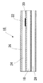
この場合、データキャリア部材16の構造としては、例えば、図2に示したような、貼着用ラベル型の構造のものが使用可能である。
すなわち、例えば、ポリエチレンテレフタレートなどの回路用基材18の表面に、導電性インクにて回路20が印刷され、その上面にICチップ22が実装されている。そして、その上面に、例えば、ポリエチレンテレフタレートなどの表面基材24が貼着され、その表面には、熱転写印字(印刷)が可能な印字コート層26が設けられている。さらに、回路用基材18の裏面側に、例えば、ポリエチレンテレフタレートなどを芯材とした両面粘着テープ28が設けられている。
In this case, as the structure of the
That is, for example, the
このように構成することによって、軸芯部材12の内径側の表面12bにデータキャリア部材16を貼着することができる。
この場合、データキャリア部材16に読み書きされる情報としては、特に限定されるものではないが、例えば、品名、品質保証期限、テープ長さ、テープ幅、ロット番号、半導体ウエハに最適な貼着圧力、貼着速度などの情報を用いることができる。
With this configuration, the
In this case, the information read from and written to the
なお、データキャリア部材16の印字コート層26に、従来のように、上記のようなデータを印字したり、バーコードを併記することも可能である。
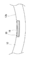
また、軸芯部材12の内径側にデータキャリア部材16を設ける場合、図3に示したように、軸芯部材12の内径側の表面12bに、データキャリア部材16の装着用凹部30を形成しておき、この装着用凹部30内に、データキャリア部材16を貼着して、軸芯部材12内に埋設した状態とすることもできる。
In addition, it is also possible to print the above data or write a barcode on the
Further, when the
この場合、装着用凹部30内にデータキャリア部材16を貼着した際に、図3に示したように、データキャリア部材16の表面16aが、軸芯部材12の内径側の表面12bと略同一平面にあるか、僅かに低い位置にあるのが、後述するように、軸芯部材12を巻き出し装置32の巻き出し軸34に脱着する際にも、脱着作業の邪魔にならず、データキャリア部材が破損損傷するおそれを考慮すれば望ましい。
In this case, when the
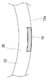
また、軸芯部材12の内径側の表面12bにデータキャリア部材16を設ける方法としては、このような貼着用ラベル型の構造のものに限定されるものではない。
例えば、図4に示したように、軸芯部材12の内径側の表面12bに形成した装着用凹部30内にデータキャリア部材16を配置した後に、その上面から合成樹脂によって樹脂封止(11)して埋設状態とする方法、図示しないが、軸芯部材12とデータキャリア部材16とを一体的に成形する方法などを採用することができる。
Further, the method of providing the
For example, as shown in FIG. 4, after the
さらに、このデータキャリア部材16を設ける位置としては、特に限定されるものではなく、この実施例では、軸芯部材12の内径側の表面12bの一端に設けたが、中央部分でもよい。また、図5に示したように、データキャリア部材16を設ける位置として、軸芯部材12の外径側の表面12aに設けるようにしてもよく、さらに、軸芯部材12の外径側の表面12aと内径側の表面12bの両方に、データキャリア部材16を設けることもできる。この場合にも、上記のように、貼着用ラベル型の構造のものに限定されるものではない。
Further, the position where the
さらに、図1に示したように、この実施例の半導体ウエハ処理テープ巻装体10の軸芯部材12には、後述するように、軸芯部材12を巻き出し装置32の巻き出し軸34に装着する際に、テープデータ読み書き装置36と、軸芯部材12の内径側に配置したデータキャリア部材16との位置合わせを正確に行うための位置あわせ部12cが形成されてい
る。
Further, as shown in FIG. 1, the
この場合、位置あわせ部12cとしては、軸芯部材12の外径側の表面12aまたは一端部に僅かに突設した突設リブ、または、切欠部の形状とすることができるが、位置合わせを行えるものであれば、マーキングでもよく、特に、その配置、形状などは限定されるものではない。
In this case, as the
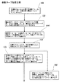
このように構成される半導体ウエハ処理テープ巻装体10は、使用に際しては、以下の図6〜図7の巻き出し装置とともに、下記のように使用される。
すなわち、図6は、図1に示した半導体ウエハ処理テープ巻装体を用いた半導体ウエハ処理テープ貼着装置の巻き出し装置の部分を示す斜視図、図7は、図6の巻き出し装置の使用方法の概略を説明する斜視図である。
The semiconductor wafer processing
6 is a perspective view showing a part of the unwinding device of the semiconductor wafer processing tape sticking apparatus using the semiconductor wafer processing tape winding body shown in FIG. 1, and FIG. 7 is a perspective view of the unwinding device of FIG. It is a perspective view explaining the outline of the usage method.
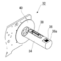
図6に示したように、半導体ウエハ処理テープ貼着装置には、巻き出し装置32が備えられており、この巻き出し装置32には、図示しない駆動モータに連結された巻き出し軸34を備えている。
As shown in FIG. 6, the semiconductor wafer processing tape sticking apparatus includes an unwinding
また、巻き出し軸34には、その外側の一端に、テープデータ読み書き装置36が設けられている。
なお、このテープデータ読み書き装置36は、巻き出し軸34の外側の一端に形成された凹部36aに形成されており、これによって、半導体ウエハ処理テープ巻装体10の軸芯部材12を、巻き出し軸34に脱着する際に、軸芯部材12の内径側の表面12bに接触して、テープデータ読み書き装置36が破損損傷しないようになっている。
The unwinding
The tape data read /
また、巻き出し軸34の中央部分には、出没自在な廻り止め部材38が、図示しない付勢部材によって、突出方向に付勢されるように設けられている。これによって、半導体ウエハ処理テープ巻装体10の軸芯部材12を、巻き出し軸34に装着した際に、巻き出し軸34の回転によって、軸芯部材12が確実に回転するように構成されている。
Further, at the central portion of the unwinding
さらに、巻き出し軸34の内側の一端には、側板部材40が設けられており、これにより、半導体ウエハ処理テープ巻装体10の軸芯部材12の端部が側板部材40に当接して、半導体ウエハ処理テープ巻装体10の位置決めが行われるように構成されている。
Further, a
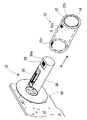
このように構成される巻き出し装置32に、半導体ウエハ処理テープ巻装体10を装着して使用する方法について、以下に説明する。
先ず、図7に示したように、半導体ウエハ処理テープ巻装体10の軸芯部材12の位置あわせ部12cを、巻き出し軸34のテープデータ読み書き装置36の位置に合致するようにする。これによって、巻き出し軸34のテープデータ読み書き装置36と、芯部材12の内径側に配置したデータキャリア部材16とが一致するようにして、データキャリア部材16に書き込まれた処理データを、巻き出し軸34のテープデータ読み書き装置36によって正確に読み取ることができる。
A method of mounting and using the semiconductor wafer processing
First, as shown in FIG. 7, the
そして、半導体ウエハ処理テープ巻装体10の軸芯部材12を、巻き出し装置32の巻き出し軸34に装着(挿着)して、半導体ウエハ処理テープ巻装体10の軸芯部材12の端部が側板部材40に当接するようにして、半導体ウエハ処理テープ巻装体10の位置決めを行う。
Then, the
この際、半導体ウエハ処理テープ巻装体10の軸芯部材12を、巻き出し軸34に装着した際に、廻り止め部材38が突出して、巻き出し軸34の回転によって、軸芯部材12が確実に回転するようになっている。
At this time, when the
また、このように半導体ウエハ処理テープ巻装体10の軸芯部材12を、巻き出し軸34に装着した状態で、軸芯部材12の内径側に配置したデータキャリア部材16に予め書き込まれた情報、例えば、品名、品質保証期限、テープ長さ、テープ幅、ロット番号、半導体ウエハに最適な貼着圧力、貼着速度などの情報を、巻き出し軸34の外側の一端に配置したテープデータ読み書き装置36によって読み取る。
In addition, information written in advance on the
そして、このテープデータ読み書き装置36によって読み取られた処理データに基づいて、図示しないテープ貼着装置によって、巻き出し装置32から巻き出された半導体ウエハ処理テープ14を、半導体ウエハに貼着することができる。
Then, based on the processing data read by the tape data read /
なお、この場合、テープ貼着装置としては、特に限定されるものではないが、例えば、半導体ウエハの裏面を研削するために、半導体ウエハの回路面を保護するための保護テープを半導体ウエハの回路面に貼着する保護テープ貼着装置、半導体ウエハの外周にリングフレームを一体化するために半導体ウエハの裏面とリングフレームに貼着するマウントテープ貼着装置を挙げることができる。 In this case, the tape adhering device is not particularly limited. For example, in order to grind the back surface of the semiconductor wafer, a protective tape for protecting the circuit surface of the semiconductor wafer is used. A protective tape sticking device for sticking to the surface and a mount tape sticking device for sticking the back surface of the semiconductor wafer and the ring frame to integrate the ring frame with the outer periphery of the semiconductor wafer can be exemplified.
従って、従来のようにホストコンピュータにアクセスすることなく、テープデータ読み書き装置36によって、データキャリア部材16に書き込まれた処理データを読み取り、読み取られた処理データに基づいて、半導体ウエハ処理テープ14を、最適条件で、半導体ウエハに貼着することが可能である。
Therefore, the processing data written on the
従って、別途、ホストコンピュータに、このような半導体ウエハ処理テープの情報を登録する必要がなく、また、加工の際にも、ホストコンピュータに登録された情報を引き出す必要もなく、各種のウエハ加工工程を行え、工程管理が簡単になる。 Therefore, it is not necessary to separately register such semiconductor wafer processing tape information in the host computer, and it is not necessary to extract information registered in the host computer during processing, and various wafer processing steps Process management.
しかも、一度使用した半導体ウエハ処理テープ14の残量、品質保証期限などの情報を、軸芯部材12に備えられたデータキャリア部材16に、テープデータ読み書き装置36によって、書き込み、ウエハ加工の際にこれらの情報を読み取ることによって、半導体ウエハ処理テープの残量不足、品質保証期限の超過などをきたすおそれがなく、工程中断や、品質の低下を招くおそれもない。
Moreover, information such as the remaining amount of the semiconductor
なお、この場合、半導体ウエハ処理テープ巻装体10の様々な半導体ウエハ処理テープ14の幅に対応できるように、図8の矢印に示したように、軸芯部材12の端部に当接する側板部材40を、図示しない移動機構によって、巻き出し軸34の軸方向に移動自在に構成してもよい。
In this case, as shown by the arrow in FIG. 8, the side plate that comes into contact with the end portion of the
また、図5に示したように、データキャリア部材16を、軸芯部材12の外径側の表面12aに設けた場合には、図6に示したような巻き出し軸34の外側の一端に配置したテープデータ読み書き装置36で読み取る代わりに、図示しないが、別途、巻き出し軸34とは別に設けたテープデータ読み書き装置で読み取ったり、ハンディータイプのテープデータ読み書き装置で読み取るようにすることも可能である。
Further, as shown in FIG. 5, when the
このように構成される本発明の半導体ウエハ処理テープ巻装体10を用いて、半導体を製造する半導体ウエハ加工処理装置および半導体ウエハ加工処理方法について、以下に、図9〜図18に基づいて説明する。
A semiconductor wafer processing apparatus and a semiconductor wafer processing method for manufacturing a semiconductor using the thus configured semiconductor wafer processing
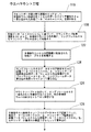
図9〜図13は、半導体ウエハ加工処理方法を説明する概略図、図14〜図18は、そのステップを説明するフローチャートである。
先ず、図9に示したように、半導体ウエハ収納カセット51に収容され、表面に回路が
形成された半導体ウエハ50を取り出して、その表面に、半導体ウエハ50の回路面を保護するための保護テープ52を、保護テープ貼着装置54を介して、半導体ウエハ50の形状に沿って保護テープ52を切断することにより、半導体ウエハ50の回路面に貼着するようになっている(保護テープ貼着工程)。
9 to 13 are schematic diagrams for explaining a semiconductor wafer processing method, and FIGS. 14 to 18 are flowcharts for explaining the steps.
First, as shown in FIG. 9, the
なお、保護テープ52としては、特に限定されるものではないが、例えば、「Adwill E-6152」(商品名)、「Adwill P-7180」(商品名)、リンテック株式会社製などが使用できる。
The
また、保護テープ貼着装置54としては、特に限定されるものではないが、例えば、「RAD-3500F/12」(商品名)、リンテック株式会社製のシステムを有する装置などが使用できる。
すなわち、この保護テープ貼着工程では、半導体ウエハ収納カセット51には、半導体ウエハ処理テープ巻装体10の軸芯部材12に配置したデータキャリア部材16と同様なデータキャリア部材51aが設けられており、このデータキャリア部材51aに書き込まれた、例えば、半導体ウエハ50のロット番号、種類、厚さなどの半導体ウエハ50に関する情報「A」を、カセットデータ読み取り装置51bよって読み取るようになっている(図14のステップ100参照)。
Further, the protective
That is, in this protective tape attaching step, the semiconductor
なお、この場合、データキャリア部材16としては、特に限定されるものではないが、例えば、「TS-L102KC」(商品名)、「TS-L301EC」(商品名)、いずれもISO 15693に準拠、
リンテック株式会社製などが使用できる。
In this case, the
Products manufactured by Lintec Corporation can be used.
また、データキャリア部材51aとしては(後述するデータキャリア部材56a、60a、66a、70a、74aも同様である)、特に限定されるものではないが、例えば、「TS-L102DC」(商品名)、「TS-L301FC」(商品名)、いずれもISO 15693に準拠、リンテッ
ク株式会社製などが使用できる。
Further, as the
また、カセットデータ読み取り装置51bとしては(後述するカセットデータ読み取り装置56c、60c、70c、74cも同様である)、特に限定されるものではないが、例えば、「LPA01」(商品名)、リンテック株式会社製などが使用できる。
The cassette
この際、保護テープ52は、上記で説明したように、半導体ウエハ処理テープ巻装体10の形態となっている。
従って、半導体ウエハ処理テープ巻装体10の軸芯部材12を、巻き出し軸34に装着することによって、軸芯部材12に配置したデータキャリア部材16に予め書き込まれた情報、例えば、品名、品質保証期限、テープ長さ、テープ幅、ロット番号、半導体ウエハに最適な貼着圧力、貼着速度などの情報「B」を、巻き出し軸34の外側の一端に配置したテープデータ読み書き装置36によって読み取るようになっている(図14のステップ102参照)。
At this time, the
Accordingly, by attaching the
この場合、テープデータ読み書き装置36としては、特に限定されるものではないが、例えば、「LPA01」(商品名)、リンテック株式会社製などが使用できる。
そして、このカセットデータ読み取り装置で読み取られた半導体ウエハ50に関する処理データ「A」と、テープデータ読み書き装置36によって読み取られた保護テープ52に関する処理データ「B」とに基づいて、保護テープ貼着装置54によって、巻き出し装置32から巻き出された保護テープ52を、半導体ウエハ50に貼着するようになっている(図14のステップ104参照)。
In this case, the tape data read /
Based on the processing data “A” related to the
従って、従来のようにホストコンピュータにアクセスすることなく、テープデータ読み書き装置36によって、データキャリア部材16に書き込まれた処理データを読み取り、
読み取られた処理データに基づいて、半導体ウエハ処理テープ14を、最適条件で、半導体ウエハに貼着することが可能である。
Therefore, the processing data written on the
Based on the read processing data, the semiconductor
そして、このように保護テープ貼着装置54によって、巻き出し装置32から巻き出された保護テープ52を、半導体ウエハ50に貼着した後、半導体ウエハ50を、別の半導体ウエハ収納カセット56に収容するようになっている(図14のステップ106参照)。
Then, after the
この際、半導体ウエハ収納カセット56には、データキャリア部材16と同様なデータキャリア部材56aが設けられており、このデータキャリア部材56aに、上記の半導体ウエハ50に関する処理データ「A」と、保護テープ52に関する処理データ「B」と、保護テープ貼着装置54によって実際に貼着加工した際の、例えば、貼着速度、貼着圧などの貼着加工に関する処理データ「C」とからなる処理データ「A+B+C」を、カセットデータ書き込み装置56bによって書き込むようになっている(図14のステップ108参照)。
At this time, the semiconductor
この場合、カセットデータ書き込み装置56bとしては(後述するカセットデータ書き込み装置60b、70bも同様である)、特に限定されるものではないが、例えば、「LPA01」(商品名)、リンテック株式会社製などが使用できる。
In this case, the cassette
なお、図示しないが、必要であれば、一度使用した保護テープ52の残量、品質保証期限などの情報を、軸芯部材12に備えられたデータキャリア部材16に、テープデータ読み書き装置36によって、書き込み、再び、例えば、別の種類の半導体ウエハ50に、保護テープ52を貼着する際にこれらの情報を読み取ることによって、保護テープ52の残量不足、品質保証期限の超過などをきたすおそれがなく、工程中断や、品質の低下を招くおそれがないようになっている(図14のステップ108’参照)。
Although not shown in the drawing, if necessary, information such as the remaining amount of the
次に、図10に示したように、半導体ウエハ収納カセット56から半導体ウエハ50を取り出して、保護テープ52が貼着された半導体ウエハ50に対して、保護テープ52側を、図示しない吸着テーブルに吸着保持して、回路が形成していない裏面を、裏面研削装置(グラインダー)58によって、所定の厚さまで研削する(裏面研削工程)。
Next, as shown in FIG. 10, the
この場合、裏面研削装置(グラインダー)58としては、特に限定されるものではないが、例えば、株式会社ディスコ製の裏面研削装置(グラインダー)に、テープデータ読み書き装置として、「LPA01」(商品名)、リンテック株式会社製を取付けた装置などが使用
できる。
In this case, the back grinding device (grinder) 58 is not particularly limited. For example, “LPA01” (trade name) is used as a tape data read / write device for a back grinding device (grinder) manufactured by DISCO Corporation. A device equipped with Lintec Corporation can be used.
すなわち、この裏面研削工程では、カセットデータ読み取り装置56cによって、半導体ウエハ収納カセット56のデータキャリア部材56aに書き込まれた上記の処理データ「A+B+C」を読み取る(図15のステップ110参照)。
That is, in this back surface grinding process, the above processing data “A + B + C” written in the
そして、半導体ウエハ収納カセット56から半導体ウエハ50を取り出して、カセットデータ読み取り装置56cによって、読み取られた処理データ「A+B+C」に基づいて、最適条件で、裏面研削装置(グラインダー)58によって、半導体ウエハ50の回路が形成していない裏面を所定の厚さまで研削する(図15のステップ112参照)。
Then, the
そして、所定の厚さまで裏面を研削した保護テープ52が貼着された半導体ウエハ50を、別の半導体ウエハ収納カセット60に収容するようになっている(図15のステップ114参照)。
Then, the
この際、半導体ウエハ収納カセット60にも、データキャリア部材60aが設けられており、このデータキャリア部材60aに、上記の処理データ「A+B+C」と、裏面研削装置(グラインダー)58によって、実際に裏面研削加工した際の、例えば、研削速度、グラインダーの目の番手情報などの裏面研削加工に関する処理データ「D」とからなる処理データ「A+B+C+D」を、カセットデータ書き込み装置60bによって書き込むようになっている(図15のステップ116参照)。
At this time, the semiconductor
その後、図11に示したように、半導体ウエハ収納カセット60から半導体ウエハ50を取り出して、マウントテープ貼着装置62によって、保護テープ52側を、吸着テーブル64に吸着保持して、この半導体ウエハ50の外周に、リングフレーム66を載置する。
After that, as shown in FIG. 11, the
この場合、マウントテープ貼着装置62としては、特に限定されるものではないが、例えば、「RAD-2700F/Sa」(商品名)、リンテック株式会社製のシステムを有する装置などが使用できる。
この状態で、上面からマウントテープ68を貼着して、リングフレーム66の外形状にマウントテープ68を切断することによって、マウントテープ68を介して、半導体ウエハ50とリングフレーム66を一体化している(ウエハマウント工程)。
In this case, the mount
In this state, the mounting
この場合、マウントテープ68としては、特に限定されるものではないが、例えば、「Adwill D-175」(商品名)、「Adwill G-36」(商品名)、リンテック株式会社製などが使用
できる。
In this case, the
なお、このウエハマウント工程においては、この半導体ウエハ50をリングフレームごと反転して、半導体ウエハ50の回路面に貼着された保護テープ52を、例えば、別途図示しない剥離テープを用いて剥離するようになっている。
In this wafer mounting process, the
すなわち、このウエハマウント工程では、カセットデータ読み取り装置60cによって、半導体ウエハ収納カセット60のデータキャリア部材60aに書き込まれた上記の処理データ「A+B+C+D」を読み取る(図16のステップ118参照)。
That is, in this wafer mounting process, the above processing data “A + B + C + D” written in the
そして、半導体ウエハ収納カセット60から半導体ウエハ50を取り出して、カセットデータ読み取り装置60cによって、読み取られた処理データ「A+B+C+D」に基づいて、最適条件で、マウントテープ貼着装置62によって、半導体ウエハ50の外周に、リングフレーム66をマウントテープ68を介して貼着して、リングフレーム66の外形状にマウントテープ68を切断することによって(または、リングフレーム66の形状に予めプリカットされたマウントテープ68を貼着することによって)、マウントテープ68を介して、半導体ウエハ50とリングフレーム66を一体化している(図16のステップ120参照)。
Then, the
半導体ウエハ50の回路面に貼着された保護テープ52を、例えば、別途図示しない剥離テープを用いて剥離する(図16のステップ122参照)。
また、リングフレーム66にも、データキャリア部材66aが設けられており、このデータキャリア部材66aに、上記の処理データ「A+B+C+D」と、マウントテープ貼着装置62によって、実際にマウントテープ貼着加工した際の、例えば、マウントテープ68の貼着速度、貼着圧力、リングフレーム66の種類、寸法、厚さなどのマウントテープ貼着加工に関する処理データ「E」とからなる処理データ「A+B+C+D+E」を、リングフレームデータ書き込み装置66bによって書き込むようになっている(図16のステップ124参照)。
The
The
そして、保護テープ52が剥離され、マウントテープ68を介して、リングフレーム6
6と一体化された半導体ウエハ50を、別の半導体ウエハ収納カセット70に収容するようになっている(図16のステップ126参照)。
Then, the
The
この際、半導体ウエハ収納カセット70にも、データキャリア部材70aが設けられており、このデータキャリア部材70aに、上記の処理データ「A+B+C+D」と、マウントテープ貼着装置62によって、実際にマウントテープ貼着加工した際の、例えば、マウントテープ68の貼着速度、貼着圧力、リングフレーム66の種類、寸法、厚さなどのマウントテープ貼着加工に関する処理データ「E」とからなる処理データ「A+B+C+D+E」を、カセットデータ書き込み装置70bによって書き込むようになっている(図16のステップ128参照)。
At this time, the semiconductor
なお、この場合、この実施例では、リングフレーム66のデータキャリア部材66aと、半導体ウエハ収納カセット70のデータキャリア部材70aの両方に、処理データ「A+B+C+D+E」を、書き込むようにしたが、いずれか一方に処理データ「A+B+C+D+E」を、書き込むようにしても構わない。
In this case, in this embodiment, the processing data “A + B + C + D + E” is written in both the
次に、図12に示したように、半導体ウエハ収納カセット70から半導体ウエハ50をリングフレーム66ごと取り出して、ダイシング装置72によって、賽の目状に切断する(ダイシング工程)。
Next, as shown in FIG. 12, the
この場合、ダイシング装置72としては、特に限定されるものではないが、例えば、株式会社ディスコ製のダイシング装置に、テープデータ読み書き装置として、「LPA01」(商品名)、リンテック株式会社製を取付けた装置などが使用できる。
In this case, the dicing
すなわち、このダイシング工程では、カセットデータ読み取り装置70cによって、半導体ウエハ収納カセット70のデータキャリア部材70aに書き込まれた上記の処理データ「A+B+C+D+E」を読み取る(図17のステップ130参照)。
That is, in this dicing process, the above processing data “A + B + C + D + E” written in the
また、半導体ウエハ収納カセット70から半導体ウエハ50を取り出して、リングフレームデータ読み取り装置66cによって、リングフレーム66のデータキャリア部材66aに書き込まれた上記の処理データ「A+B+C+D+E」を読み取る(図17のステップ132参照)。
Further, the
この場合、リングフレームデータ読み取り装置66cとしては(後述するリングフレームデータ読み取り装置66eも同様である)、特に限定されるものではないが、例えば、「LPA01」(商品名)、リンテック株式会社製などが使用できる。
In this case, the ring frame
そして、これらのカセットデータ読み取り装置70c、リングフレームデータ読み取り装置66cによって、読み取られた処理データ「A+B+C+D+E」に基づいて、最適条件で、ダイシング装置72によって、半導体ウエハ50を賽の目状に切断する(図17のステップ134参照)。
Then, based on the processing data “A + B + C + D + E” read by the cassette
なお、この実施例では、これらのカセットデータ読み取り装置70c、リングフレームデータ読み取り装置66cによって、読み取られた処理データ「A+B+C+D+E」に基づいて、ダイシング装置72によって、半導体ウエハ50を賽の目状に切断したが、いずれか一方の処理データ「A+B+C+D+E」を、読み込むようにしても構わない。
In this embodiment, the
また、リングフレーム66のデータキャリア部材66aに、上記の処理データ「A+B+C+D+E」と、ダイシング装置72によって、実際にダイシング加工した際の、例えば、ダイシング装置72のダイシング刃の回転速度、ダイシング寸法などのダイシング加
工に関する処理データ「F」とからなる処理データ「A+B+C+D+E+F」を、リングフレームデータ書き込み装置66dによって書き込むようになっている(図17のステップ136参照)。
Further, when the processing data “A + B + C + D + E” and the dicing
この場合、リングフレームデータ書き込み装置66dとしては、特に限定されるものではないが、例えば、「LPA01」(商品名)、リンテック株式会社製などが使用できる。
そして、ダイシング装置72によって、賽の目状に切断された半導体ウエハ50を、リングフレーム66ごと、別の半導体ウエハ収納カセット74に収容するようになっている(図17のステップ138参照)。
In this case, the ring frame
The dicing
この際、半導体ウエハ収納カセット74にも、データキャリア部材74aが設けられており、このデータキャリア部材74aに、上記の処理データ「A+B+C+D+E」と、ダイシング装置72によって、実際にダイシング加工した際の、例えば、ダイシング装置72のダイシング刃の回転速度、ダイシング寸法などのダイシング加工に関する処理データ「F」とからなる処理データ「A+B+C+D+E+F」を、カセットデータ書き込み装置74bによって書き込むようになっている(図17のステップ140参照)。
At this time, the semiconductor
なお、この場合、この実施例では、リングフレーム66のデータキャリア部材66aと、半導体ウエハ収納カセット74のデータキャリア部材74aの両方に、処理データ「A+B+C+D+E+F」を、書き込むようにしたが、いずれか一方に処理データ「A+B+C+D+E+F」を、書き込むようにしても構わない。
In this case, in this embodiment, the processing data “A + B + C + D + E + F” is written in both the
その後、図13に示したように、半導体ウエハ収納カセット74から半導体ウエハ50をリングフレーム66ごと取り出して、ボンディング装置76によって、賽の目状に切断された半導体チップをピックアップして、電子部品78の電子部品実装部に装着している(ダイボンディング工程)。
Thereafter, as shown in FIG. 13, the
この場合、ボンディング装置76としては、特に限定されるものではないが、例えば、株式会社新川製のボンディング装置に、テープデータ読み書き装置として、「LPA01」(商品名)、リンテック株式会社製を取付けた装置などが使用できる。
In this case, the
すなわち、このダイボンディング工程では、カセットデータ読み取り装置74cによって、半導体ウエハ収納カセット74のデータキャリア部材74aに書き込まれた上記の処理データ「A+B+C+D+E+F」を読み取る(図18のステップ142参照)。
That is, in this die bonding process, the above processing data “A + B + C + D + E + F” written on the
また、半導体ウエハ収納カセット74から半導体ウエハ50を取り出して、リングフレームデータ読み取り装置66eによって、リングフレーム66のデータキャリア部材66aに書き込まれた上記の処理データ「A+B+C+D+E+F」を読み取る(図18のステップ144参照)。
Further, the
そして、これらのカセットデータ読み取り装置74c、リングフレームデータ読み取り装置66eによって、読み取られた処理データ「A+B+C+D+E+F」に基づいて、最適条件で、ボンディング装置76によって、賽の目状に切断された半導体チップ50aをピックアップして、電子部品78の電子部品実装部に装着する(図18のステップ146参照)。
Based on the processing data “A + B + C + D + E + F” read by the cassette data reading device 74c and ring frame
なお、この実施例では、カセットデータ読み取り装置74c、リングフレームデータ読み取り装置66eによって、読み取られた処理データ「A+B+C+D+E+F」に基づいて、ボンディング装置76によって、賽の目状に切断された半導体チップ50aをピックアップして、電子部品78の電子部品実装部に装着するようにしたが、いずれか一方の
処理データ「A+B+C+D+E+F」を、読み込むようにしても構わない。
In this embodiment, the
また、上記の実施例では、半導体ウエハ収納カセットにデータキャリア部材を設ける方法、配置位置、リングフレーム66にデータキャリア部材66aを設ける方法、配置位置などは特に限定されるものではない。
In the above-described embodiment, the method and arrangement position of providing the data carrier member in the semiconductor wafer storage cassette, the method and arrangement position of providing the
すなわち、半導体ウエハ処理テープ巻装体10の軸芯部材12に備えられたデータキャリア部材16と同様に、貼着用ラベル型の構造のもの、装着用凹部内にデータキャリア部材を配置した後に、その上面から合成樹脂によって樹脂封止して埋設状態とする方法、これらの半導体ウエハ収納カセットまたはリングフレーム66と、データキャリア部材16とを一体的に成形する方法などを採用することができる。
That is, in the same manner as the
また、半導体ウエハ収納カセットにデータキャリア部材を設ける位置としては、この実施例では、半導体ウエハ収納カセットの底部に設け、これに応じて、カセットデータ読み取り装置、カセットデータ書き込み装置を半導体ウエハ収納カセットの底部に対峙する位置に設けている。 In this embodiment, the position where the data carrier member is provided in the semiconductor wafer storage cassette is provided at the bottom of the semiconductor wafer storage cassette, and accordingly, the cassette data reading device and the cassette data writing device are connected to the semiconductor wafer storage cassette. It is provided at a position facing the bottom.
しかしながら、半導体ウエハ収納カセットにデータキャリア部材を設ける位置としては、これに何ら限定されるものではなく、半導体ウエハ収納カセットの上部、側部、背面部など適宜変更可能であり、これに応じて、カセットデータ読み取り装置、カセットデータ書き込み装置を半導体ウエハ収納カセットの上部、側部、背面部などに対峙する位置に設ければよい。
However, the position where the data carrier member is provided in the semiconductor wafer storage cassette is not limited to this, and can be changed as appropriate, such as the upper part, side part, and rear part of the semiconductor wafer storage cassette. cassette data reader, a cassette data writing apparatus of the semiconductor wafer storage cassette top, side, may be provided at a position facing the such as the back portion.
さらに、この実施例では、リングフレームデータ読み取り装置を、リングフレーム66のデータキャリア部材66aと対峙する位置に固定するように設けている。しかしながら、リングフレームデータ読み取り装置を、半導体ウエハ収納カセットから半導体ウエハ50を取り出す吸着アームなどの取り出し操作装置の先端に設けて、半導体ウエハ50を取り出す際に、リングフレーム66のデータキャリア部材66aの処理データを読み取るようにしてもよい。
Further, in this embodiment, the ring frame data reading device is provided so as to be fixed at a position facing the
同様に、リングフレームデータ書き込み装置についても、半導体ウエハ収納カセットに半導体ウエハ50を収容する吸着アームなどの収容操作装置の先端に設けて、半導体ウエハ50を収容する際に、リングフレーム66のデータキャリア部材66aに処理データを書き込むようにしてもよい。
Similarly, the ring frame data writing device is also provided at the tip of a storage operation device such as a suction arm for storing the
このような半導体ウエハ加工処理方法によれば、例えば、品名、品質保証期限、テープ長さ、テープ幅、ロット番号、半導体ウエハに最適な貼着圧力、貼着速度などの情報を、軸芯部材12に備えられたデータキャリア部材16に書き込むことができる。
According to such a semiconductor wafer processing method, for example, information such as product name, quality assurance deadline, tape length, tape width, lot number, optimum adhesion pressure for semiconductor wafer, adhesion speed, etc. 12 can be written on the
これにより、半導体ウエハ50にこの半導体ウエハ処理テープ巻装体10に巻装された半導体ウエハ処理テープ14(保護テープ52、マウントテープ68)を貼着して半導体ウエハ50の各種のウエハ加工を行う際に、従来のようにホストコンピュータにアクセスすることなく、半導体ウエハ処理テープ巻装体10の軸芯部材12に備えられたデータキャリア部材16、半導体ウエハ収納カセットのデータキャリア部材、リングフレーム66のデータキャリア部材66aに書き込まれた処理データを読み取り、読み取られた処理データに基づいて、半導体ウエハ処理テープを用いて、最適条件でウェハ加工処理することが可能である。
As a result, the semiconductor wafer processing tape 14 (
従って、別途、ホストコンピュータに、このような半導体ウエハ処理テープの情報を登録する必要がなく、また、加工の際にも、ホストコンピュータに登録された情報を引き出す必要もなく、各種のウエハ加工工程を行え、工程管理が簡単になる。 Therefore, it is not necessary to separately register such semiconductor wafer processing tape information in the host computer, and it is not necessary to extract information registered in the host computer during processing, and various wafer processing steps Process management.
しかも、一度使用した半導体ウエハ処理テープの残量、品質保証期限などの情報を、軸芯部材12に備えられたデータキャリア部材16に書き込み、ウエハ加工の際にこれらの情報を読み取ることによって、半導体ウエハ処理テープの残量不足、品質保証期限の超過などをきたすおそれがなく、工程中断や、品質の低下を招くおそれもない。
Moreover, by writing information such as the remaining amount of the semiconductor wafer processing tape once used and the quality guarantee deadline to the
以上、本発明の好ましい実施の態様を説明してきたが、本発明はこれに限定されることはなく、例えば、誤った半導体ウエハ処理テープ巻装体10を、巻き出し装置32に装着した場合、半導体ウエハ処理テープの品質保証期限が切れた場合、裏面研削装置(グラインダー)58の砥石部材の使用回数、ダイシング装置72のダイシング刃の使用回数などが、使用限界を超えた場合に、警告を出すようにすることもでき、作業員のミスを防止することができる。
The preferred embodiment of the present invention has been described above, but the present invention is not limited to this. For example, when the wrong semiconductor wafer processing
さらに、半導体ウエハ処理テープ巻装体10の軸芯部材12、半導体ウエハ収納カセット、リングフレーム66を回収して、これらのデータキャリア部材に書き込まれた処理データを初期化することによって、半導体ウエハ収納カセット、リングフレーム66を再使用することもできる。
Further, by collecting the
さらに、この実施例では、各工程の装置を別々の装置、すなわち、いわゆるスタンドアローン型の装置としたが、これらを連続的に一つの装置内で処理するいわゆるインライン型の装置とすることも可能である。このようなインライン型の装置の場合には、上述したような半導体ウエハ収納カセットの数、カセットデータ読み取り装置の数を低減できることになる。この場合には、リングフレーム66のデータキャリア部材66aによって、上記したような処理データを書き込み、読み取るようにすればよい。
Furthermore, in this embodiment, each process apparatus is a separate apparatus, that is, a so-called stand-alone apparatus, but it is also possible to use a so-called in-line apparatus that continuously processes these in one apparatus. It is. In the case of such an inline apparatus, the number of semiconductor wafer storage cassettes and the number of cassette data reading apparatuses as described above can be reduced. In this case, the processing data as described above may be written and read by the
また、この実施例では、取り出し側の半導体ウエハ収納カセットと、所定のウエハ加工を終了した半導体ウエハを収容する半導体ウエハ収納カセットを別々のものにしたが、同一の半導体ウエハ収納カセットに、一枚ずつ半導体ウエハを取り出し、ウエハ加工終了後に収容することも可能である。 Further, in this embodiment, the semiconductor wafer storage cassette on the take-out side and the semiconductor wafer storage cassette for storing the semiconductor wafers for which predetermined wafer processing has been completed are separated, but one sheet is placed in the same semiconductor wafer storage cassette. It is also possible to take out the semiconductor wafers one by one and store them after the wafer processing is completed.
さらに、図示しないホストコンピュータから、不足のデータ、管理データなどを、各ウエハ処理工程のそれぞれの装置に入力、制御するようにしたり、それぞれのデータキャリア部材に、書き込む(入力)するようにすることも可能である。 In addition, from a host computer (not shown), insufficient data, management data, and the like are input to and controlled by each device in each wafer processing step, and are written (input) to each data carrier member. Is also possible.
また、上記実施例では、いわゆる「後ダイシング法」について説明したが、ウェハの回路が形成された表面よりウェハ厚さ方向に所定深さまでダイシングして、賽の目状に有底の溝を形成する工程、ウェハ表面に保護テープを貼着する工程、ウェハ裏面を有底の溝に至るまで研削して多数のチップに分割する工程、保護テープが貼着されたウェハをリングフレームに貼着する工程、保護テープを剥離する工程の順で行う「先ダイシング法」においても用いることも可能であるなど本発明の目的を逸脱しない範囲で種々の変更が可能である。 In the above embodiment, the so-called “post-dicing method” has been described. However, the step of dicing to a predetermined depth in the wafer thickness direction from the surface on which the circuit of the wafer is formed forms a bottomed groove in the shape of a ridge. , A process of attaching a protective tape to the wafer surface, a process of grinding the back surface of the wafer up to a bottomed groove and dividing it into a large number of chips, a process of attaching the wafer with the protective tape attached to a ring frame, Various modifications can be made without departing from the object of the present invention, such as the “first dicing method” that is performed in the order of the process of peeling off the protective tape.
10 半導体ウエハ処理テープ巻装体
12a 表面
12b 表面
12 軸芯部材
12c 位置あわせ部
14 半導体ウエハ処理テープ
16 データキャリア部材
16a 表面
18 回路用基材
20 回路
22 ICチップ
24 表面基材
26 印字コート層
28 両面粘着テープ
30 装着用凹部
32 巻き出し装置
34 巻き出し軸
36a 凹部
36 テープデータ読み書き装置
38 廻り止め部材
40 側板部材
50 半導体ウエハ
50a 半導体チップ
51 半導体ウエハ収納カセット
51a データキャリア部材
51b カセットデータ読み取り装置
52 保護テープ
54 保護テープ貼着装置
56 半導体ウエハ収納カセット
56a データキャリア部材
56b カセットデータ書き込み装置
56c カセットデータ読み取り装置
58 裏面研削装置
60 半導体ウエハ収納カセット
60a データキャリア部材
60b カセットデータ書き込み装置
60c カセットデータ読み取り装置
62 マウントテープ貼着装置
64 吸着テーブル
66 リングフレーム
66a データキャリア部材
66b リングフレームデータ書き込み装置
66c リングフレームデータ読み取り装置
66d リングフレームデータ書き込み装置
66e リングフレームデータ読み取り装置
68 マウントテープ
70 半導体ウエハ収納カセット
70a データキャリア部材
70b カセットデータ書き込み装置
70c カセットデータ読み取り装置
72 ダイシング装置
74 半導体ウエハ収納カセット
74a データキャリア部材
74c カセットデータ読み取り装置
76 ボンディング装置
78 電子部品
200 半導体ウエハ
201 半導体ウエハ収納カセット
202 保護テープ
204 保護テープ貼着装置
206 半導体ウエハ収納カセット
208 裏面研削装置
210 半導体ウエハ収納カセット
212 吸着テーブル
214 リングフレーム
216 マウントテープ
218 半導体ウエハ収納カセット
220 ダイシング装置
222 半導体ウエハ収納カセット
224 ボンディング装置
226 電子部品
228 ホストコンピュータ
DESCRIPTION OF SYMBOLS 10 Semiconductor wafer processing tape winding body 12a Surface 12b Surface 12 Axis core member 12c Positioning part 14 Semiconductor wafer processing tape 16 Data carrier member 16a Surface 18 Circuit base material 20 Circuit 22 IC chip 24 Surface base material 26 Print coat layer 28 Double-sided adhesive tape 30 mounting recess 32 unwinding device 34 unwinding shaft 36a recess 36 tape data read / write device 38 anti-rotation member 40 side plate member 50 semiconductor wafer 50a semiconductor chip 51 semiconductor wafer storage cassette 51a data carrier member 51b cassette data reading device 52 Protective tape 54 Protective tape attaching device 56 Semiconductor wafer storage cassette 56a Data carrier member 56b Cassette data writing device 56c Cassette data reading device 58 Back surface grinding device 60 Semiconductor wafer storage cassette 60a Data carrier member 60b Cassette data writing device 60c Cassette data reading device 62 Mount tape sticking device 64 Suction table 66 Ring frame 66a Data carrier member 66b Ring frame data writing device 66c Ring frame data reading device 66d Ring frame data writing device 66e Ring frame data reading device 68 Mount tape 70 Semiconductor wafer storage cassette 70a Data carrier member 70b Cassette data writing device 70c Cassette data reading device 72 Dicing device 74 Semiconductor wafer storage cassette 74a Data carrier member 74c Cassette data reading device 76 Bonding device 78 Electronic components 200 Semiconductor wafer 201 Semiconductor wafer storage cassette 202 Protective tape 204 Protective tape attaching device 206 Semiconductor wafer storage cassette 208 Back surface grinding device 210 Semiconductor wafer storage cassette 212 Suction table 214 Ring frame 216 Mount tape 218 Semiconductor wafer storage cassette 220 Dicing device 222 Semiconductor wafer storage cassette 224 Bonding device 226 Electronic component 228 Host computer
Claims (40)
前記半導体ウエハ処理テープを巻装した軸芯部材と、
前記軸芯部材に備えられ、所定の処理データを読み書き可能なデータキャリア部材と、
を備え、
前記データキャリア部材が、ICチップと、このICチップに接続された導電性コイルとから構成されるRFメモリーである非接触型のデータキャリア部材であり、
前記軸芯部材に、前記データキャリア部材に対応した位置あわせ部が形成されており、
前記所定の処理データが、半導体ウエハ処理テープの品名、品質保証期限、テープ長さ、テープ幅、ロット番号を含む情報データであることを特徴とする半導体ウエハ処理テープ巻装体。 A semiconductor wafer processing tape for processing a semiconductor wafer by sticking to the semiconductor wafer;
An axial core member wound with the semiconductor wafer processing tape;
A data carrier member provided on the shaft core member and capable of reading and writing predetermined processing data;
Equipped with a,
The data carrier member is a non-contact type data carrier member which is an RF memory composed of an IC chip and a conductive coil connected to the IC chip.
An alignment portion corresponding to the data carrier member is formed on the shaft core member,
The semiconductor wafer processing tape winding body, wherein the predetermined processing data is information data including a semiconductor wafer processing tape product name, a quality guarantee period, a tape length, a tape width, and a lot number .
該データキャリア装着用凹部に、前記データキャリア部材が装着されていることを特徴とする請求項1または2に記載の半導体ウエハ処理テープ巻装体。 3. The semiconductor wafer processing tape winding body according to claim 1, wherein the data carrier member is mounted in the concave portion for mounting the data carrier.
前記半導体ウエハ処理テープ巻装体のデータキャリア部材に書き込まれた処理データを読み書きするテープデータ読み書き装置と、
前記テープデータ読み書き装置によって読み取られた処理データに基づいて、巻き出し装置から巻き出された半導体ウエハ処理テープを、半導体ウエハに貼着するテープ貼着装置とを備え、
前記テープデータ読み書き装置が、巻き出し軸に備えられ、
前記半導体ウエハ処理テープ巻装体のデータキャリア部材に書き込まれた処理データが、半導体ウエハ処理テープの品名、品質保証期限、テープ長さ、テープ幅、ロット番号を含む情報データであることを特徴とする半導体ウエハ処理テープ貼着装置。 An unwinding device comprising an unwinding shaft capable of detachably mounting the semiconductor wafer processing tape winding body according to any one of claims 1 to 5 ;
A tape data read / write device for reading / writing process data written on a data carrier member of the semiconductor wafer processing tape winding body;
Based on the processing data read by the tape data read / write device, a semiconductor wafer processing tape unwound from the unwinding device, and a tape sticking device for sticking to the semiconductor wafer ,
The tape data read / write device is provided on the unwinding shaft,
The processing data written on the data carrier member of the semiconductor wafer processing tape winding body is information data including the product name, quality guarantee period, tape length, tape width, and lot number of the semiconductor wafer processing tape. Semiconductor wafer processing tape sticking device.
前記半導体ウエハ収納カセットに設けられたデータキャリア部材に、所定の処理データを書き込むカセットデータ書き込み装置を備えることを特徴とする請求項6から10のいずれかに記載の半導体ウエハ処理テープ貼着装置。 For a semiconductor wafer storage cassette for storing a semiconductor wafer to which a semiconductor wafer processing tape is attached by the tape attaching device,
11. The semiconductor wafer processing tape sticking apparatus according to claim 6, further comprising a cassette data writing device for writing predetermined processing data on a data carrier member provided in the semiconductor wafer storage cassette.
半導体ウエハ処理テープの品名、品質保証期限、テープ長さ、テープ幅、ロット番号、半導体ウエハに最適な貼着圧力、貼着速度のうちの少なくともいずれかからなる半導体ウエハ処理テープに関する情報データ、 Semiconductor wafer processing tape product name, quality assurance deadline, tape length, tape width, lot number, optimum bonding pressure for semiconductor wafer, information data on semiconductor wafer processing tape consisting of at least one of the bonding speed,
半導体ウエハの種類、厚さ、加工工程における加工条件のうちの少なくともいずれかからなる半導体ウエハに関する情報データ、 Information data on the semiconductor wafer comprising at least one of the type, thickness, and processing conditions in the processing step of the semiconductor wafer;
のうちの少なくともいずれかからなる情報データであることを特徴とする請求項11に記載の半導体ウエハ処理テープ貼着装置。12. The semiconductor wafer processing tape sticking apparatus according to claim 11, wherein the data is information data consisting of at least one of the above.
半導体ウエハ処理テープの品名、品質保証期限、テープ長さ、テープ幅、ロット番号、半導体ウエハに最適な貼着圧力、貼着速度のうちの少なくともいずれかからなる半導体ウエハ処理テープに関する情報データ、 Semiconductor wafer processing tape product name, quality assurance deadline, tape length, tape width, lot number, optimum bonding pressure for semiconductor wafer, information data on semiconductor wafer processing tape consisting of at least one of the bonding speed,
半導体ウエハの種類、厚さ、加工工程における加工条件のうちの少なくともいずれかからなる半導体ウエハに関する情報データ、 Information data on the semiconductor wafer comprising at least one of the type, thickness, and processing conditions in the processing step of the semiconductor wafer;
のうちの少なくともいずれかからなる情報データであることを特徴とする請求項14または15に記載の半導体ウエハ処理テープ貼着装置。16. The semiconductor wafer processing tape sticking apparatus according to claim 14 or 15, wherein the data is information data comprising at least one of the above.
前工程で所定の加工処理が行われた半導体ウエハを収納する、半導体ウエハ収納カセットに設けられたデータキャリア部材に書き込まれた処理データを読み取る、カセットデータ読み取り装置を備え、
前記カセットデータ読み取り装置で読み取られた処理データと、前記テープデータ読み書き装置によって読み取られた処理データに基づいて、テープ貼着装置によって、半導体ウエハ処理テープを、半導体ウエハに貼着するように構成されていることを特徴とする請求項6から16のいずれかに記載の半導体ウエハ処理テープ貼着装置。 The semiconductor wafer processing tape sticking device is
A cassette data reader is provided for storing the semiconductor wafer that has been subjected to the predetermined processing in the previous process, and for reading the processing data written on the data carrier member provided in the semiconductor wafer storage cassette.
Based on the processing data read by the cassette data reader and the processing data read by the tape data read / write device, the semiconductor wafer processing tape is attached to the semiconductor wafer by the tape attaching device. The semiconductor wafer processing tape sticking apparatus according to claim 6 , wherein the semiconductor wafer processing tape sticking apparatus is provided.
前記テープ貼着装置によって半導体ウエハ処理テープが貼着された半導体ウエハを収納する、半導体ウエハ収納カセットに設けられたデータキャリア部材に書き込まれた処理データに基づいて、所定のウエハ加工処理を行うように構成したことを特徴とする半導体ウエハ加工処理装置。 The semiconductor wafer processing tape attaching apparatus according to any one of claims 6 to 17 , with respect to the semiconductor wafer to which the semiconductor wafer processing tape is attached,
A predetermined wafer processing process is performed based on processing data written in a data carrier member provided in a semiconductor wafer storage cassette for storing a semiconductor wafer having a semiconductor wafer processing tape attached thereto by the tape attaching device. A semiconductor wafer processing apparatus characterized by comprising:
前記リングフレームに設けられたデータキャリア部材に書き込まれた処理データに基づいて、所定のウエハ加工処理を行うように構成したことを特徴とする半導体ウエハ加工処理装置。 The semiconductor wafer processing tape attaching apparatus according to any one of claims 14 to 17 , with respect to the semiconductor wafer to which the semiconductor wafer processing tape is attached,
A semiconductor wafer processing apparatus configured to perform predetermined wafer processing based on processing data written on a data carrier member provided in the ring frame.
前記保護テープ巻装体を、脱着自在に装着可能な巻き出し軸を備えた巻き出し装置と、 An unwinding device equipped with an unwinding shaft capable of detachably mounting the protective tape winding body; and
前記巻き出し装置から巻き出された保護テープを、半導体ウエハに貼着する保護テープ貼着装置と、を備える保護テープ貼着システムであって、 A protective tape sticking system comprising a protective tape sticking device for sticking the protective tape unwound from the unwinding device to a semiconductor wafer,
前記保護テープ巻装体に設けられたデータキャリア部材に書き込まれた処理データを読み書きするテープデータ読み書き装置をさらに備え、 A tape data read / write device for reading / writing processing data written on a data carrier member provided in the protective tape winding body;
前記保護テープ巻装体に、前記データキャリア部材に対応した位置あわせ部が形成されており、 An alignment part corresponding to the data carrier member is formed on the protective tape winding body,
前記保護テープ巻装体のデータキャリア部材に書き込まれた保護テープに関する情報を、前記テープデータ読み書き装置によって読み取り、 Information on the protective tape written on the data carrier member of the protective tape winding body is read by the tape data read / write device,
前記保護テープに関する情報に基づいて、前記保護テープ貼着装置によって、前記保護テープを半導体ウエハに貼着することを特徴とする保護テープ貼着システム。 Based on the information regarding the said protective tape, the said protective tape sticking apparatus adheres the said protective tape to a semiconductor wafer by the said protective tape sticking apparatus.
前記保護テープを貼着した後の半導体ウエハを収納する第2の半導体ウエハ収納カセットに設けられたデータキャリア部材に、所定の処理データを書き込むカセットデータ書き込み装置と、をさらに備え、 A cassette data writing device for writing predetermined processing data to a data carrier member provided in a second semiconductor wafer storage cassette for storing the semiconductor wafer after the protective tape is attached;
前記第1の半導体ウエハ収納カセットのデータキャリア部材に書き込まれた半導体ウエハに関する情報を、前記カセットデータ読み取り装置によって読み取り、 Reading information on the semiconductor wafer written on the data carrier member of the first semiconductor wafer storage cassette by the cassette data reader;
前記半導体ウエハに関する情報と、前記保護テープに関する情報とに基づいて、前記保護テープ貼着装置によって、前記保護テープを半導体ウエハに貼着し、 Based on the information on the semiconductor wafer and the information on the protective tape, the protective tape sticking device attaches the protective tape to the semiconductor wafer,
該半導体ウエハを、前記第2の半導体ウエハ収納カセットに収容するとともに、第2の半導体ウエハ収納カセットのデータキャリア部材に、前記半導体ウエハに関する情報と、前記保護テープに関する情報と、保護テープ貼着加工に関する情報とを、前記カセットデータ書き込み装置によって書き込むことを特徴とする請求項23に記載の保護テープ貼着システム。 The semiconductor wafer is accommodated in the second semiconductor wafer storage cassette, and information on the semiconductor wafer, information on the protective tape, and protective tape attaching processing are performed on a data carrier member of the second semiconductor wafer storage cassette. 24. The protective tape sticking system according to claim 23, wherein the information on the tape is written by the cassette data writing device.
前記保護テープ巻装体を、脱着自在に装着可能な巻き出し軸を備えた巻き出し装置と、 An unwinding device equipped with an unwinding shaft capable of detachably mounting the protective tape winding body; and
前記巻き出し装置から巻き出された保護テープを、半導体ウエハに貼着する保護テープ貼着装置と、を備える保護テープ貼着システムであって、 A protective tape sticking system comprising a protective tape sticking device for sticking the protective tape unwound from the unwinding device to a semiconductor wafer,
前記保護テープを貼着する前の半導体ウエハが収納される第1の半導体ウエハ収納カセットに設けられたデータキャリア部材に書き込まれた処理データを読み取るカセットデータ読み取り装置と、 A cassette data reading device for reading processing data written in a data carrier member provided in a first semiconductor wafer storage cassette in which a semiconductor wafer before the protective tape is attached is stored;
前記保護テープ巻装体に設けられたデータキャリア部材に書き込まれた処理データを読み書きするテープデータ読み書き装置と、 A tape data read / write device for reading / writing processing data written on a data carrier member provided in the protective tape winding body;
前記保護テープを貼着した後の半導体ウエハを収納する第2の半導体ウエハ収納カセットに設けられたデータキャリア部材に、所定の処理データを書き込むカセットデータ書き込み装置と、をさらに備え、 A cassette data writing device for writing predetermined processing data to a data carrier member provided in a second semiconductor wafer storage cassette for storing the semiconductor wafer after the protective tape is attached;
前記第1の半導体ウエハ収納カセットのデータキャリア部材に書き込まれた半導体ウエハに関する情報を、前記カセットデータ読み取り装置によって読み取り、 Reading information on the semiconductor wafer written on the data carrier member of the first semiconductor wafer storage cassette by the cassette data reader;
前記保護テープ巻装体のデータキャリア部材に書き込まれた保護テープに関する情報を、前記テープデータ読み書き装置によって読み取り、 Information on the protective tape written on the data carrier member of the protective tape winding body is read by the tape data read / write device,
前記半導体ウエハに関する情報と、前記保護テープに関する情報とに基づいて、前記保護テープ貼着装置によって、前記保護テープを半導体ウエハに貼着し、 Based on the information on the semiconductor wafer and the information on the protective tape, the protective tape sticking device attaches the protective tape to the semiconductor wafer,
該半導体ウエハを、前記第2の半導体ウエハ収納カセットに収容するとともに、第2の半導体ウエハ収納カセットのデータキャリア部材に、前記半導体ウエハに関する情報と、前記保護テープに関する情報と、保護テープ貼着加工に関する情報とを、前記カセットデータ書き込み装置によって書き込むことを特徴とする保護テープ貼着システム。 The semiconductor wafer is accommodated in the second semiconductor wafer storage cassette, and information on the semiconductor wafer, information on the protective tape, and protective tape attaching processing are performed on a data carrier member of the second semiconductor wafer storage cassette. Information on the tape is written by the cassette data writing device.
裏面研削加工が行われる前の半導体ウエハが収容される第1の半導体ウエハ収納カセットに設けられたデータキャリア部材に書き込まれた処理データを読み取るカセットデータ読み取り装置と、 A cassette data reading device for reading processing data written on a data carrier member provided in a first semiconductor wafer storage cassette in which a semiconductor wafer before back surface grinding processing is stored;
裏面研削加工が行われた後の半導体ウエハを収容する第2の半導体ウエハ収納カセットに設けられたデータキャリア部材に、所定の処理データを書き込むカセットデータ書き込み装置と、を備え、 A cassette data writing device for writing predetermined processing data to a data carrier member provided in a second semiconductor wafer storage cassette for storing a semiconductor wafer after the back surface grinding is performed,
前記第1の半導体ウエハ収納カセットのデータキャリア部材に書き込まれた半導体ウエハに関する情報と、保護テープに関する情報と、保護テープ貼着加工に関する情報とを読み取り、 Read information on the semiconductor wafer written on the data carrier member of the first semiconductor wafer storage cassette, information on the protective tape, and information on the protective tape attaching process,
前記半導体ウエハに関する情報と、前記保護テープに関する情報と、前記保護テープ貼着加工に関する情報とに基づいて、前記裏面研削装置によって前記半導体ウエハの裏面を所定の厚さまで研削し、 Based on information on the semiconductor wafer, information on the protective tape, and information on the protective tape attaching process, the back surface of the semiconductor wafer is ground to a predetermined thickness by the back surface grinding device,
該半導体ウエハを前記第2の半導体ウエハ収納カセットに収容するとともに、第2の半導体ウエハ収納カセットのデータキャリア部材に、前記半導体ウエハに関する情報と、前記保護テープに関する情報と、前記保護テープ貼着加工に関する情報と、裏面研削加工処理に関する情報とを、前記カセットデータ書き込み装置によって書き込むことを特徴とする半導体ウエハの裏面研削システム。 The semiconductor wafer is accommodated in the second semiconductor wafer storage cassette, and the data carrier member of the second semiconductor wafer storage cassette is provided with information on the semiconductor wafer, information on the protective tape, and the protective tape attaching process. The semiconductor wafer back surface grinding system is characterized in that the information related to the back surface processing and the information related to the back surface grinding processing are written by the cassette data writing device.
前記半導体ウエハに関する情報が、半導体ウエハの種類、厚さのうちの少なくともいずれかであることを特徴とする請求項28に記載の半導体ウエハの裏面研削システム。 29. The backside grinding system for a semiconductor wafer according to claim 28, wherein the information on the semiconductor wafer is at least one of a type and a thickness of the semiconductor wafer.
前記マウントテープ巻装体を、脱着自在に装着可能な巻き出し軸を備えた巻き出し装置と、 An unwinding device equipped with an unwinding shaft capable of detachably mounting the mount tape winding body; and
前記巻き出し装置から巻き出されたマウントテープを、半導体ウエハと該半導体ウエハの外周に載置したリングフレームが一体となるように貼着するマウントテープ貼着装置と、 A mount tape affixing device for adhering the mount tape unwound from the unwinder so that the semiconductor wafer and the ring frame placed on the outer periphery of the semiconductor wafer are integrated;
を備え、With
保護テープ貼着加工、及び、裏面研削加工が行われた半導体ウエハの外周に、マウントテープを介してリングフレームを貼着する半導体ウエハのウエハマウントシステムであって、 A wafer mounting system for a semiconductor wafer in which a ring frame is attached to the outer periphery of a semiconductor wafer subjected to a protective tape attaching process and a back surface grinding process via a mount tape,
前記マウントテープを貼着する前の半導体ウエハが収容される第1の半導体ウエハ収納カセットに設けられたデータキャリア部材に書き込まれた処理データを読み取るカセットデータ読み取り装置と、 A cassette data reading device that reads processing data written on a data carrier member provided in a first semiconductor wafer storage cassette in which a semiconductor wafer before the mounting tape is attached is stored;
前記マウントテープを貼着した後の半導体ウエハを収容する第2の半導体ウエハ収納カセットに設けられたデータキャリア部材に、所定の処理データを書き込むカセットデータ書き込み装置と、をさらに備え、 A cassette data writing device for writing predetermined processing data to a data carrier member provided in a second semiconductor wafer storage cassette for storing the semiconductor wafer after the mounting tape is attached;
前記第1の半導体ウエハ収納カセットのデータキャリア部材に書き込まれた半導体ウエハに関する情報と、保護テープに関する情報と、保護テープ貼着加工に関する情報と、裏面研削加工に関する情報とを読み取り、 Read information on the semiconductor wafer written on the data carrier member of the first semiconductor wafer storage cassette, information on the protective tape, information on the protective tape attaching process, and information on the back surface grinding process,
前記半導体ウエハに関する情報と、前記保護テープに関する情報と、前記保護テープ貼着加工に関する情報と、前記裏面研削加工に関する情報とに基づいて、前記マウントテープ貼着装置によって、前記マウントテープを、半導体ウエハと該半導体ウエハの外周に載置したリングフレームとが一体となるように貼着し、 Based on the information on the semiconductor wafer, the information on the protective tape, the information on the protective tape attaching process, and the information on the back surface grinding process, the mounting tape is attached to the semiconductor wafer by the mount tape attaching apparatus. And a ring frame placed on the outer periphery of the semiconductor wafer so as to be integrated,
前記半導体ウエハの回路面に貼着された保護テープを剥離し、 Peel off the protective tape attached to the circuit surface of the semiconductor wafer,
前記半導体ウエハを前記第2の半導体ウエハ収納カセットに収容するとともに、第2の半導体ウエハ収納カセットのデータキャリア部材に、前記半導体ウエハに関する情報と、前記保護テープに関する情報と、前記保護テープ貼着加工に関する情報と、前記裏面研削加工に関する情報と、前記マウントテープ貼着加工処理に関する情報とを、前記カセットデータ書き込み装置によって書き込むことを特徴とする半導体ウエハのウエハマウントシステム。 The semiconductor wafer is accommodated in the second semiconductor wafer storage cassette, and the information on the semiconductor wafer, the information on the protective tape, and the protective tape pasting process on the data carrier member of the second semiconductor wafer storage cassette The wafer mounting system for a semiconductor wafer, wherein the information relating to the back surface grinding and the information relating to the mounting tape attaching process are written by the cassette data writing device.
前記リングフレームのデータキャリア部材に、前記半導体ウエハに関する情報と、前記保護テープに関する情報と、前記保護テープ貼着加工に関する情報と、前記裏面研削加工に関する情報と、マウントテープ貼着加工処理に関する情報とを、前記リングフレームデータ書き込み装置によって書き込むことを特徴とする請求項30に記載の半導体ウエハのウエハマウントシステム。 On the data carrier member of the ring frame, information about the semiconductor wafer, information about the protective tape, information about the protective tape attaching process, information about the back surface grinding process, information about the mount tape attaching process, 31. The wafer mounting system for a semiconductor wafer according to claim 30, wherein the wafer frame is written by the ring frame data writing device.
前記半導体ウエハに関する情報が、半導体ウエハの種類、厚さのうちの少なくともいずれかからなる情報であることを特徴とする請求項30または31に記載の半導体ウエハのウエハマウントシステム。 32. The wafer mounting system for a semiconductor wafer according to claim 30, wherein the information about the semiconductor wafer is information consisting of at least one of a type and a thickness of the semiconductor wafer.
賽の目状に切断される前の半導体ウエハが収容される第1の半導体ウエハ収納カセットに設けられたデータキャリア部材に書き込まれた処理データを読み取るカセットデータ読み取り装置と、 A cassette data reading device for reading processing data written on a data carrier member provided in a first semiconductor wafer storage cassette in which a semiconductor wafer before being cut into a basket shape is stored;
賽の目状に切断された後の半導体ウエハを収容する第2の半導体ウエハ収納カセットに設けられたデータキャリア部材に、所定の処理データを書き込むカセットデータ書き込み装置と、を備え、 A cassette data writing device for writing predetermined processing data on a data carrier member provided in a second semiconductor wafer storage cassette for storing a semiconductor wafer after being cut into a cage shape,
前記第1の半導体ウエハ収納カセットのデータキャリア部材に書き込まれた半導体ウエハに関する情報と、保護テープに関する情報と、保護テープ貼着加工に関する情報と、裏面研削加工に関する情報と、マウントテープ貼着加工処理に関する情報とを読み取り、 Information relating to the semiconductor wafer written on the data carrier member of the first semiconductor wafer storage cassette, information relating to the protective tape, information relating to the protective tape attaching process, information relating to the back surface grinding process, and mounting tape attaching process And read information about
前記半導体ウエハに関する情報と、前記保護テープに関する情報と、前記保護テープ貼着加工に関する情報と、前記裏面研削加工に関する情報と、前記マウントテープ貼着加工処理に関する情報とに基づいて、前記ダイシング装置によって、半導体ウエハを賽の目状に切断し、 Based on the information on the semiconductor wafer, the information on the protective tape, the information on the protective tape attaching process, the information on the back surface grinding process, and the information on the mount tape attaching process, by the dicing apparatus , Cut the semiconductor wafer into the shape of a ridge,
前記半導体ウエハを前記第2の半導体ウエハ収納カセットに収容するとともに、第2の半導体ウエハ収納カセットのデータキャリア部材に、前記半導体ウエハに関する情報と、前記保護テープに関する情報と、前記保護テープ貼着加工に関する情報と、前記裏面研削加工に関する情報と、前記マウントテープ貼着加工処理に関する情報と、ダイシング加工処理に関する情報とを、前記カセットデータ書き込み装置によって書き込むことを特徴とする半導体ウエハのダイシングシステム。 The semiconductor wafer is accommodated in the second semiconductor wafer storage cassette, and the information on the semiconductor wafer, the information on the protective tape, and the protective tape pasting process on the data carrier member of the second semiconductor wafer storage cassette Information about the back surface grinding process, information about the mount tape attaching process, and information about the dicing process are written by the cassette data writing device.
前記リングフレームのデータキャリア部材に書き込まれた半導体ウエハに関する情報と、保護テープに関する情報と、保護テープ貼着加工に関する情報と、裏面研削加工に関する情報と、マウントテープ貼着加工処理に関する情報とを読み取り、 Reads information on the semiconductor wafer written on the data carrier member of the ring frame, information on the protective tape, information on the protective tape attaching process, information on the back surface grinding process, and information on the mount tape attaching process ,
前記半導体ウエハに関する情報と、前記保護テープに関する情報と、前記保護テープ貼着加工に関する情報と、前記裏面研削加工に関する情報と、前記マウントテープ貼着加工処理に関する情報とに基づいて、前記ダイシング装置によって、半導体ウエハを賽の目状に切断することを特徴とする請求項33に記載の半導体ウエハのダイシングシステム。 Based on the information on the semiconductor wafer, the information on the protective tape, the information on the protective tape attaching process, the information on the back surface grinding process, and the information on the mount tape attaching process, by the dicing apparatus 34. The semiconductor wafer dicing system according to claim 33, wherein the semiconductor wafer is cut into a grid shape.
前記ダイシング装置によって、半導体ウエハを賽の目状に切断した後に、前記リングフレームのデータキャリア部材に、前記半導体ウエハに関する情報と、前記保護テープに関する情報と、前記保護テープ貼着加工に関する情報と、前記裏面研削加工に関する情報と、前記マウントテープ貼着加工処理に関する情報と、ダイシング加工処理に関する情報とを、前記リングフレームデータ書き込み装置によって書き込むことを特徴とする請求項33または34に記載の半導体ウエハのダイシングシステム。 After the semiconductor wafer is cut into a square shape by the dicing device, information on the semiconductor wafer, information on the protective tape, information on the protective tape attaching process, and information on the back surface of the data carrier member of the ring frame 35. The dicing of a semiconductor wafer according to claim 33 or 34, wherein information relating to grinding, information relating to the mounting tape attaching process, and information relating to a dicing process are written by the ring frame data writing device. system.
前記半導体ウエハに関する情報が、半導体ウエハの種類、厚さのうちの少なくともいずれかからなる情報であることを特徴とする請求項33から35のいずれかに記載の半導体ウエハのダイシングシステム。 36. The semiconductor wafer dicing system according to claim 33, wherein the information about the semiconductor wafer is information including at least one of a type and a thickness of the semiconductor wafer.
前記半導体ウエハが収容される半導体ウエハ収納カセットに設けられたデータキャリア部材に書き込まれた処理データを読み取るカセットデータ読み取り装置を備え、 A cassette data reading device that reads processing data written on a data carrier member provided in a semiconductor wafer storage cassette in which the semiconductor wafer is stored;
前記半導体ウエハ収納カセットのデータキャリア部材に書き込まれた半導体ウエハに関する情報と、保護テープに関する情報と、保護テープ貼着加工に関する情報と、裏面研削加工に関する情報と、マウントテープ貼着加工処理に関する情報と、ダイシング加工処理に関する情報とを読み取り、 Information on the semiconductor wafer written on the data carrier member of the semiconductor wafer storage cassette, information on the protective tape, information on the protective tape attaching process, information on the back surface grinding process, and information on the mount tape attaching process , Read information about the dicing process,
前記半導体ウエハに関する情報と、前記保護テープに関する情報と、前記保護テープ貼着加工に関する情報と、前記裏面研削加工に関する情報と、前記マウントテープ貼着加工処理に関する情報と、前記ダイシング加工処理に関する情報とに基づいて、前記ボンディング装置によって、賽の目状に切断された半導体チップをピックアップして、前記電子部品の電子部品実装部に装着することを特徴とする半導体ウエハのダイボンディングシステム。 Information about the semiconductor wafer, information about the protective tape, information about the protective tape attaching process, information about the back surface grinding process, information about the mount tape attaching process, and information about the dicing process The semiconductor wafer die bonding system is characterized in that the bonding device picks up a semiconductor chip cut into a grid shape and mounts it on the electronic component mounting portion of the electronic component.
前記リングフレームのデータキャリア部材に書き込まれた半導体ウエハに関する情報と、保護テープに関する情報と、保護テープ貼着加工に関する情報と、裏面研削加工に関する情報と、マウントテープ貼着加工処理に関する情報と、ダイシング加工処理に関する情報とを読み取り、 Information on the semiconductor wafer written on the data carrier member of the ring frame, information on the protective tape, information on the protective tape attaching process, information on the back surface grinding process, information on the mounting tape attaching process, and dicing Read information about processing,
前記半導体ウエハに関する情報と、前記保護テープに関する情報と、前記保護テープ貼着加工に関する情報と、前記裏面研削加工に関する情報と、前記マウントテープ貼着加工処理に関する情報と、前記ダイシング加工処理に関する情報とに基づいて、前記ボンディング装置によって、賽の目状に切断された半導体チップをピックアップして、前記電子部品の電子部品実装部に装着することを特徴とする請求項37に記載の半導体ウエハのダイボンディングシステム。 Information about the semiconductor wafer, information about the protective tape, information about the protective tape attaching process, information about the back surface grinding process, information about the mount tape attaching process, and information about the dicing process 38. The semiconductor wafer die bonding system according to claim 37, wherein the semiconductor device is picked up by the bonding apparatus in accordance with the above, and is mounted on an electronic component mounting portion of the electronic component. .
前記半導体ウエハに関する情報が、半導体ウエハの種類、厚さのうちの少なくともいずれかからなる情報であることを特徴とする請求項37または38に記載の半導体ウエハのダイボンディングシステム。 39. The semiconductor wafer die bonding system according to claim 37 or 38, wherein the information on the semiconductor wafer is information comprising at least one of a type and a thickness of the semiconductor wafer.
請求項28または29に記載の裏面研削システムと、 A back grinding system according to claim 28 or 29;
請求項30から32のいずれかに記載のウエハマウントシステムと、 A wafer mounting system according to any of claims 30 to 32;
請求項33から36のいずれかに記載のダイシングシステムと、 A dicing system according to any of claims 33 to 36;
請求項37から39のいずれかに記載のダイボンディングシステムと、 A die bonding system according to any of claims 37 to 39;
を備える半導体ウエハ加工処理システム。A semiconductor wafer processing system comprising:
Priority Applications (9)
| Application Number | Priority Date | Filing Date | Title |
|---|---|---|---|
| JP2005190388A JP4541237B2 (en) | 2005-06-29 | 2005-06-29 | Semiconductor wafer processing tape winding body, semiconductor wafer processing tape sticking apparatus using the same, and semiconductor wafer processing apparatus |
| SG200604375A SG128646A1 (en) | 2005-06-29 | 2006-06-27 | Semiconductor wafer processing tape winding body, semiconductor wafer processing tape sticking apparatus and semiconductor wafer processing apparatus that use the semiconductor wafer processing tape winding body |
| TW095123279A TWI408738B (en) | 2005-06-29 | 2006-06-28 | Winding device for winding semiconductor wafer processing tape, bonding device using such winding device for bonding semiconductor wafer processing tape, and semiocnductor wafer processing device |
| US11/476,382 US8392011B2 (en) | 2005-06-29 | 2006-06-28 | Semiconductor wafer processing tape winding body, semiconductor wafer processing tape sticking apparatus and semiconductor wafer processing apparatus that use the semiconductor wafer processing tape winding body |
| KR1020060058380A KR101269290B1 (en) | 2005-06-29 | 2006-06-28 | Semiconductor wafer processing tape winding body, semiconductor wafer processing tape sticking apparatus and semiconductor wafer processing apparatus that use the semiconductor wafer processing tape winding body |
| MYPI20063109A MY143974A (en) | 2005-06-29 | 2006-06-29 | Semiconductor wafer processing tape winding body,semiconductors wafer processing tape sticking apparatus and semiconductors wafer processing apparatus that use the semiconductors wafer processing tape winding body |
| DE102006029961.2A DE102006029961B4 (en) | 2005-06-29 | 2006-06-29 | A winding body with a processing tape for a semiconductor wafer, and an apparatus for adhering a processing tape to a semiconductor wafer using the winding body with the processing tape for the semiconductor wafer |
| CN2006101007304A CN1892982B (en) | 2005-06-29 | 2006-06-29 | Semiconductor wafer processing tape winding body, semiconductor wafer processing tape sticking apparatus and semiconductor wafer processing apparatus that use the semiconductor wafer processing tape w |
| GB0612953A GB2428136B (en) | 2005-06-29 | 2006-06-29 | Semiconductor wafer processing tape winding body, semiconductor wafer processing tape sticking apparatus and semiconductor wafer processing apparatus |
Applications Claiming Priority (1)
| Application Number | Priority Date | Filing Date | Title |
|---|---|---|---|
| JP2005190388A JP4541237B2 (en) | 2005-06-29 | 2005-06-29 | Semiconductor wafer processing tape winding body, semiconductor wafer processing tape sticking apparatus using the same, and semiconductor wafer processing apparatus |
Publications (3)
| Publication Number | Publication Date |
|---|---|
| JP2007012807A JP2007012807A (en) | 2007-01-18 |
| JP2007012807A5 JP2007012807A5 (en) | 2008-05-15 |
| JP4541237B2 true JP4541237B2 (en) | 2010-09-08 |
Family
ID=36888336
Family Applications (1)
| Application Number | Title | Priority Date | Filing Date |
|---|---|---|---|
| JP2005190388A Active JP4541237B2 (en) | 2005-06-29 | 2005-06-29 | Semiconductor wafer processing tape winding body, semiconductor wafer processing tape sticking apparatus using the same, and semiconductor wafer processing apparatus |
Country Status (9)
| Country | Link |
|---|---|
| US (1) | US8392011B2 (en) |
| JP (1) | JP4541237B2 (en) |
| KR (1) | KR101269290B1 (en) |
| CN (1) | CN1892982B (en) |
| DE (1) | DE102006029961B4 (en) |
| GB (1) | GB2428136B (en) |
| MY (1) | MY143974A (en) |
| SG (1) | SG128646A1 (en) |
| TW (1) | TWI408738B (en) |
Families Citing this family (12)
| Publication number | Priority date | Publication date | Assignee | Title |
|---|---|---|---|---|
| JP4841262B2 (en) * | 2006-02-13 | 2011-12-21 | 株式会社東京精密 | Wafer processing equipment |
| JP4693696B2 (en) * | 2006-06-05 | 2011-06-01 | 株式会社東京精密 | Work processing device |
| US8688254B2 (en) * | 2007-06-15 | 2014-04-01 | Taiwan Semiconductor Manufacturing Company, Ltd. | Multiple tools using a single data processing unit |
| JP5089531B2 (en) * | 2007-08-31 | 2012-12-05 | 大日本印刷株式会社 | Wafer fixing jig |
| TWI417967B (en) * | 2009-11-02 | 2013-12-01 | Chroma Ate Inc | A method for marking a grain bearing tray, a sorting machine and a characteristic mark |
| JP5690615B2 (en) * | 2011-03-03 | 2015-03-25 | リンテック株式会社 | Ring frame and process management system |
| JP5856397B2 (en) * | 2011-06-30 | 2016-02-09 | リンテック株式会社 | Shaft core member |
| JP6105312B2 (en) | 2013-02-13 | 2017-03-29 | リンテック株式会社 | Support device and data management method |
| JP6740444B2 (en) * | 2017-02-20 | 2020-08-12 | 株式会社Fuji | Splicing tape management system |
| JP2020198408A (en) * | 2019-06-05 | 2020-12-10 | 株式会社ディスコ | Tape unit and tape pasting machine |
| JP7351703B2 (en) * | 2019-10-09 | 2023-09-27 | 株式会社ディスコ | tape mounter |
| US11904538B2 (en) * | 2020-11-27 | 2024-02-20 | The Boeing Company | Systems and methods for simultaneously manufacturing a plurality of objects |
Citations (6)
| Publication number | Priority date | Publication date | Assignee | Title |
|---|---|---|---|---|
| JP2000281268A (en) * | 1999-03-30 | 2000-10-10 | Sato Corp | Roll-shaped printed medium |
| JP2001203523A (en) * | 2000-01-19 | 2001-07-27 | Dainippon Printing Co Ltd | Removable ic tag for winding |
| JP2001354343A (en) * | 2000-06-14 | 2001-12-25 | Sato Corp | Belt-like roll body, printer, and method of printing |
| JP2003006481A (en) * | 2001-06-19 | 2003-01-10 | Seiko Epson Corp | Sales system for rolled paper with memory and form sales system |
| JP2005136305A (en) * | 2003-10-31 | 2005-05-26 | Lintec Corp | Table for sticking device |
| JP2005162335A (en) * | 2003-11-28 | 2005-06-23 | Sato Corp | Winding core for roll product |
Family Cites Families (42)
| Publication number | Priority date | Publication date | Assignee | Title |
|---|---|---|---|---|
| US3643849A (en) * | 1970-02-25 | 1972-02-22 | Midwestern Instr Inc | Tape guide |
| DE3234345A1 (en) * | 1982-09-16 | 1984-03-22 | Robert Bosch Gmbh, 7000 Stuttgart | CODING SYSTEM FOR DETECTING INFORMATION FROM WORKPIECE CARRIERS AND THE LIKE |
| JPH0616524B2 (en) | 1984-03-12 | 1994-03-02 | 日東電工株式会社 | Adhesive thin plate for fixing semiconductor wafers |
| JPS60223139A (en) | 1984-04-18 | 1985-11-07 | Nitto Electric Ind Co Ltd | Bonding sheet for fixing semiconductor wafer |
| JP2601956B2 (en) | 1991-07-31 | 1997-04-23 | リンテック株式会社 | Removable adhesive polymer |
| JP3216205B2 (en) | 1992-03-27 | 2001-10-09 | 神鋼電機株式会社 | ID recognition device in semiconductor manufacturing system |
| JP2984549B2 (en) | 1994-07-12 | 1999-11-29 | リンテック株式会社 | Energy ray-curable pressure-sensitive adhesive composition and method of using the same |
| US5673195A (en) * | 1995-06-12 | 1997-09-30 | Schwartz; Vladimir | Compact disc tracking system and method |
| DE59711634D1 (en) * | 1996-08-09 | 2004-06-24 | Ferag Ag | Movable object with electronically stored contactlessly readable and / or overwritable data |
| US5907492A (en) * | 1997-06-06 | 1999-05-25 | Micron Technology, Inc. | Method for using data regarding manufacturing procedures integrated circuits (IC's) have undergone, such as repairs, to select procedures the IC's will undergo, such as additional repairs |
| WO2000002236A2 (en) * | 1998-07-07 | 2000-01-13 | Memc Electronic Materials, Inc. | Radio frequency identification system and method for tracking silicon wafers |
| DE19842951C1 (en) * | 1998-09-18 | 2000-06-21 | Siemens Nixdorf Inf Syst | Automatic placement machine with identification device for component containers |
| EP1455302B1 (en) * | 1999-02-24 | 2007-09-19 | Hitachi Maxell, Ltd. | Method for manufacturing an IC element including a coil |
| JP2000331962A (en) * | 1999-05-18 | 2000-11-30 | Lintec Corp | Method for working semiconductor wafer and semiconductor wafer support member |
| JP2001019278A (en) * | 1999-07-07 | 2001-01-23 | Asahi Chem Ind Co Ltd | Core |
| US6405096B1 (en) * | 1999-08-10 | 2002-06-11 | Advanced Micro Devices, Inc. | Method and apparatus for run-to-run controlling of overlay registration |
| US6427093B1 (en) * | 1999-10-07 | 2002-07-30 | Advanced Micro Devices, Inc. | Method and apparatus for optimal wafer-by-wafer processing |
| US6640151B1 (en) * | 1999-12-22 | 2003-10-28 | Applied Materials, Inc. | Multi-tool control system, method and medium |
| JP2001332521A (en) * | 2000-05-19 | 2001-11-30 | Sony Corp | Method and device for transferring chip-like semiconductor device |
| US6524881B1 (en) | 2000-08-25 | 2003-02-25 | Micron Technology, Inc. | Method and apparatus for marking a bare semiconductor die |
| US6351684B1 (en) * | 2000-09-19 | 2002-02-26 | Advanced Micro Devices, Inc. | Mask identification database server |
| JP3446830B2 (en) * | 2000-10-16 | 2003-09-16 | 宮崎沖電気株式会社 | Apparatus and method for attaching tape to semiconductor wafer |
| US6700729B1 (en) * | 2000-10-17 | 2004-03-02 | Hewlett-Packard Development Company | Alignment marks for tape head positioning |
| US6996449B2 (en) * | 2001-07-31 | 2006-02-07 | Asahi Kasei Microsystems Co., Ltd. | Semiconductor manufacturing apparatus control system |
| US7016753B2 (en) * | 2001-10-30 | 2006-03-21 | Semiconductor Energy Laboratory Co., Ltd. | Management system for production line and management method for production line |
| US20030090829A1 (en) * | 2001-11-14 | 2003-05-15 | Johnson Kristianne E. | Apparatus for and method of retrieving data cartridge-related information from a data cartridge memory |
| US20030123174A1 (en) * | 2001-12-28 | 2003-07-03 | Mark Hennecken | Continuously variable storage device data transfer rate |
| US6582973B1 (en) * | 2002-04-05 | 2003-06-24 | Texas Instruments Incorporated | Method for controlling a semiconductor manufacturing process |
| US6940678B2 (en) * | 2002-04-10 | 2005-09-06 | Seagate Technology Llc | Magnetic alignment marking of hard disks |
| US6716651B2 (en) * | 2002-04-25 | 2004-04-06 | Taiwan Semiconductor Manufacturing Co., Ltd | Method and apparatus for identifying a wafer cassette |
| US20040004789A1 (en) * | 2002-07-03 | 2004-01-08 | Christopher Watanabe | Replaceable memory element in a single reel tape cartridge |
| CN1711593A (en) * | 2002-11-04 | 2005-12-21 | 皇家飞利浦电子股份有限公司 | Storage system using superparamagnetic particles |
| US7273166B2 (en) * | 2002-11-11 | 2007-09-25 | Fuji Machine Mfg. Co., Ltd. | Component information applying method and apparatus |
| JP2004284601A (en) | 2003-03-19 | 2004-10-14 | Renesas Technology Corp | Method for carrying, mounting and packaging semi-conductor device, and method for reusing stored article |
| EP1498935B1 (en) * | 2003-07-15 | 2006-04-26 | Tokyo Seimitsu Co.,Ltd. | Device for calculating the quantity of light and method thereof |
| JP4444619B2 (en) * | 2003-10-10 | 2010-03-31 | リンテック株式会社 | MOUNTING DEVICE AND MOUNTING METHOD |
| JP4494753B2 (en) * | 2003-10-27 | 2010-06-30 | リンテック株式会社 | Sheet peeling apparatus and peeling method |
| JP4495960B2 (en) * | 2003-12-26 | 2010-07-07 | キヤノンItソリューションズ株式会社 | Model creation device for the relationship between process and quality |
| JP2005209850A (en) * | 2004-01-22 | 2005-08-04 | Toshiba Corp | Design system and manufacturing system of semiconductor device |
| US20050283266A1 (en) | 2004-06-17 | 2005-12-22 | Geraci Gwen R | Method and system for providing unit level traceability of semiconductor die |
| TWI234234B (en) | 2004-08-09 | 2005-06-11 | Touch Micro System Tech | Method of segmenting a wafer |
| JP4916243B2 (en) | 2006-08-02 | 2012-04-11 | 大阪瓦斯株式会社 | Microbubble generator |
-
2005
- 2005-06-29 JP JP2005190388A patent/JP4541237B2/en active Active
-
2006
- 2006-06-27 SG SG200604375A patent/SG128646A1/en unknown
- 2006-06-28 TW TW095123279A patent/TWI408738B/en active
- 2006-06-28 US US11/476,382 patent/US8392011B2/en active Active
- 2006-06-28 KR KR1020060058380A patent/KR101269290B1/en active IP Right Grant
- 2006-06-29 GB GB0612953A patent/GB2428136B/en active Active
- 2006-06-29 DE DE102006029961.2A patent/DE102006029961B4/en active Active
- 2006-06-29 MY MYPI20063109A patent/MY143974A/en unknown
- 2006-06-29 CN CN2006101007304A patent/CN1892982B/en active Active
Patent Citations (6)
| Publication number | Priority date | Publication date | Assignee | Title |
|---|---|---|---|---|
| JP2000281268A (en) * | 1999-03-30 | 2000-10-10 | Sato Corp | Roll-shaped printed medium |
| JP2001203523A (en) * | 2000-01-19 | 2001-07-27 | Dainippon Printing Co Ltd | Removable ic tag for winding |
| JP2001354343A (en) * | 2000-06-14 | 2001-12-25 | Sato Corp | Belt-like roll body, printer, and method of printing |
| JP2003006481A (en) * | 2001-06-19 | 2003-01-10 | Seiko Epson Corp | Sales system for rolled paper with memory and form sales system |
| JP2005136305A (en) * | 2003-10-31 | 2005-05-26 | Lintec Corp | Table for sticking device |
| JP2005162335A (en) * | 2003-11-28 | 2005-06-23 | Sato Corp | Winding core for roll product |
Also Published As
| Publication number | Publication date |
|---|---|
| SG128646A1 (en) | 2007-01-30 |
| DE102006029961B4 (en) | 2022-02-17 |
| KR20070001808A (en) | 2007-01-04 |
| DE102006029961A1 (en) | 2007-07-05 |
| KR101269290B1 (en) | 2013-05-29 |
| GB2428136A (en) | 2007-01-17 |
| GB2428136B (en) | 2009-09-23 |
| TW200707566A (en) | 2007-02-16 |
| CN1892982B (en) | 2012-06-27 |
| MY143974A (en) | 2011-07-29 |
| US20070162175A1 (en) | 2007-07-12 |
| GB0612953D0 (en) | 2006-08-09 |
| TWI408738B (en) | 2013-09-11 |
| CN1892982A (en) | 2007-01-10 |
| US8392011B2 (en) | 2013-03-05 |
| JP2007012807A (en) | 2007-01-18 |
Similar Documents
| Publication | Publication Date | Title |
|---|---|---|
| JP4541237B2 (en) | Semiconductor wafer processing tape winding body, semiconductor wafer processing tape sticking apparatus using the same, and semiconductor wafer processing apparatus | |
| KR100468748B1 (en) | Dicing tape mounter applicable a pre-cut dicing tape and general dicing tape and In-line system having the dicing tape mounter | |
| JP2004047823A (en) | Dicing tape sticking device and back grind dicing tape sticking system | |
| JP2007048885A (en) | Frame for dicing of semiconductor wafer | |
| KR100637569B1 (en) | Method of processing semiconductor wafer and semiconductor wafer supporting member | |
| JP2005123653A (en) | Taping/peering apparatus and taping system | |
| KR20180123018A (en) | Substrate transfer method and substrate transfer apparatus | |
| WO2007046234A1 (en) | Measuring device | |
| JP4693542B2 (en) | Semiconductor wafer dicing frame | |
| JP4809648B2 (en) | Manufacturing method of electronic device | |
| JP2008293508A (en) | Semiconductor wafer machining method and semiconductor wafer support member | |
| JP5690615B2 (en) | Ring frame and process management system | |
| JP4693545B2 (en) | Semiconductor wafer dicing frame | |
| JPWO2019044506A1 (en) | Board processing system and board processing method | |
| JP2006172166A (en) | Packaging method and packaging apparatus for ic chip, and manufacturing method of contactless identification tag | |
| JPH07276870A (en) | Ic carrier with plate-shaped frame body, manufacture thereof and ic carrier case | |
| JP3120051U (en) | RFID label with magnetic sheet | |
| JP5590937B2 (en) | Attaching the ring label | |
| JP4473559B2 (en) | Labeling device | |
| JPH10177776A (en) | Cassette label and video cassette tape | |
| JP4537773B2 (en) | Labeling system | |
| JP5718579B2 (en) | Toroidal label sticker | |
| JP5035975B2 (en) | Wireless tag | |
| TWI329563B (en) | ||
| KR20230042640A (en) | Protection sheet and protection sheet adhesion apparatus |
Legal Events
| Date | Code | Title | Description |
|---|---|---|---|
| A521 | Request for written amendment filed |
Free format text: JAPANESE INTERMEDIATE CODE: A523 Effective date: 20080401 |
|
| A621 | Written request for application examination |
Free format text: JAPANESE INTERMEDIATE CODE: A621 Effective date: 20080401 |
|
| A977 | Report on retrieval |
Free format text: JAPANESE INTERMEDIATE CODE: A971007 Effective date: 20100324 |
|
| A131 | Notification of reasons for refusal |
Free format text: JAPANESE INTERMEDIATE CODE: A131 Effective date: 20100330 |
|
| A521 | Request for written amendment filed |
Free format text: JAPANESE INTERMEDIATE CODE: A523 Effective date: 20100531 |
|
| TRDD | Decision of grant or rejection written | ||
| A01 | Written decision to grant a patent or to grant a registration (utility model) |
Free format text: JAPANESE INTERMEDIATE CODE: A01 Effective date: 20100615 |
|
| A01 | Written decision to grant a patent or to grant a registration (utility model) |
Free format text: JAPANESE INTERMEDIATE CODE: A01 |
|
| A61 | First payment of annual fees (during grant procedure) |
Free format text: JAPANESE INTERMEDIATE CODE: A61 Effective date: 20100623 |
|
| R150 | Certificate of patent or registration of utility model |
Ref document number: 4541237 Country of ref document: JP Free format text: JAPANESE INTERMEDIATE CODE: R150 Free format text: JAPANESE INTERMEDIATE CODE: R150 |
|
| FPAY | Renewal fee payment (event date is renewal date of database) |
Free format text: PAYMENT UNTIL: 20130702 Year of fee payment: 3 |
|
| R250 | Receipt of annual fees |
Free format text: JAPANESE INTERMEDIATE CODE: R250 |
|
| R250 | Receipt of annual fees |
Free format text: JAPANESE INTERMEDIATE CODE: R250 |
|
| R250 | Receipt of annual fees |
Free format text: JAPANESE INTERMEDIATE CODE: R250 |
|
| R250 | Receipt of annual fees |
Free format text: JAPANESE INTERMEDIATE CODE: R250 |
|
| R250 | Receipt of annual fees |
Free format text: JAPANESE INTERMEDIATE CODE: R250 |
|
| R250 | Receipt of annual fees |
Free format text: JAPANESE INTERMEDIATE CODE: R250 |
|
| R250 | Receipt of annual fees |
Free format text: JAPANESE INTERMEDIATE CODE: R250 |
|
| R250 | Receipt of annual fees |
Free format text: JAPANESE INTERMEDIATE CODE: R250 |
|
| R250 | Receipt of annual fees |
Free format text: JAPANESE INTERMEDIATE CODE: R250 |
|
| R250 | Receipt of annual fees |
Free format text: JAPANESE INTERMEDIATE CODE: R250 |
|
| R250 | Receipt of annual fees |
Free format text: JAPANESE INTERMEDIATE CODE: R250 |