JP4539752B2 - Method for forming quantum well structure and method for manufacturing semiconductor light emitting device - Google Patents
Method for forming quantum well structure and method for manufacturing semiconductor light emitting device Download PDFInfo
- Publication number
- JP4539752B2 JP4539752B2 JP2008101781A JP2008101781A JP4539752B2 JP 4539752 B2 JP4539752 B2 JP 4539752B2 JP 2008101781 A JP2008101781 A JP 2008101781A JP 2008101781 A JP2008101781 A JP 2008101781A JP 4539752 B2 JP4539752 B2 JP 4539752B2
- Authority
- JP
- Japan
- Prior art keywords
- layer
- source gas
- well layer
- temperature
- well
- Prior art date
- Legal status (The legal status is an assumption and is not a legal conclusion. Google has not performed a legal analysis and makes no representation as to the accuracy of the status listed.)
- Expired - Fee Related
Links
- 239000004065 semiconductor Substances 0.000 title claims abstract description 89
- 238000000034 method Methods 0.000 title claims abstract description 62
- 238000004519 manufacturing process Methods 0.000 title claims abstract description 30
- 239000000203 mixture Substances 0.000 claims abstract description 95
- 230000004888 barrier function Effects 0.000 claims abstract description 70
- JMASRVWKEDWRBT-UHFFFAOYSA-N Gallium nitride Chemical compound [Ga]#N JMASRVWKEDWRBT-UHFFFAOYSA-N 0.000 claims abstract description 36
- XCZXGTMEAKBVPV-UHFFFAOYSA-N trimethylgallium Chemical compound C[Ga](C)C XCZXGTMEAKBVPV-UHFFFAOYSA-N 0.000 claims abstract description 30
- 239000007789 gas Substances 0.000 claims description 77
- 229910002601 GaN Inorganic materials 0.000 claims description 62
- 230000012010 growth Effects 0.000 claims description 51
- 239000000758 substrate Substances 0.000 claims description 28
- 229910052738 indium Inorganic materials 0.000 claims description 25
- APFVFJFRJDLVQX-UHFFFAOYSA-N indium atom Chemical compound [In] APFVFJFRJDLVQX-UHFFFAOYSA-N 0.000 claims description 24
- IBEFSUTVZWZJEL-UHFFFAOYSA-N trimethylindium Chemical group C[In](C)C IBEFSUTVZWZJEL-UHFFFAOYSA-N 0.000 claims description 23
- 150000004767 nitrides Chemical class 0.000 claims description 10
- GYHNNYVSQQEPJS-UHFFFAOYSA-N Gallium Chemical group [Ga] GYHNNYVSQQEPJS-UHFFFAOYSA-N 0.000 claims description 7
- 229910052733 gallium Inorganic materials 0.000 claims description 7
- IJGRMHOSHXDMSA-UHFFFAOYSA-N Atomic nitrogen Chemical compound N#N IJGRMHOSHXDMSA-UHFFFAOYSA-N 0.000 claims description 6
- 229910052757 nitrogen Inorganic materials 0.000 claims description 3
- 239000007858 starting material Substances 0.000 abstract 2
- 239000013078 crystal Substances 0.000 description 17
- 238000007796 conventional method Methods 0.000 description 14
- 235000012431 wafers Nutrition 0.000 description 14
- 229910002704 AlGaN Inorganic materials 0.000 description 11
- 230000008859 change Effects 0.000 description 11
- 230000000694 effects Effects 0.000 description 10
- 239000002994 raw material Substances 0.000 description 10
- 238000000295 emission spectrum Methods 0.000 description 7
- 230000009471 action Effects 0.000 description 6
- 238000005424 photoluminescence Methods 0.000 description 6
- 238000010586 diagram Methods 0.000 description 5
- 238000010348 incorporation Methods 0.000 description 4
- QGZKDVFQNNGYKY-UHFFFAOYSA-N Ammonia Chemical compound N QGZKDVFQNNGYKY-UHFFFAOYSA-N 0.000 description 2
- 235000005811 Viola adunca Nutrition 0.000 description 2
- 240000009038 Viola odorata Species 0.000 description 2
- 235000013487 Viola odorata Nutrition 0.000 description 2
- 235000002254 Viola papilionacea Nutrition 0.000 description 2
- 238000005229 chemical vapour deposition Methods 0.000 description 2
- 238000002425 crystallisation Methods 0.000 description 2
- 230000008025 crystallization Effects 0.000 description 2
- 239000002019 doping agent Substances 0.000 description 2
- 125000005842 heteroatom Chemical group 0.000 description 2
- 239000000463 material Substances 0.000 description 2
- 229910052751 metal Inorganic materials 0.000 description 2
- 239000002184 metal Substances 0.000 description 2
- 150000002736 metal compounds Chemical class 0.000 description 2
- 238000002441 X-ray diffraction Methods 0.000 description 1
- 229910021529 ammonia Inorganic materials 0.000 description 1
- 230000015572 biosynthetic process Effects 0.000 description 1
- 238000005253 cladding Methods 0.000 description 1
- 239000000470 constituent Substances 0.000 description 1
- 239000013256 coordination polymer Substances 0.000 description 1
- 230000005684 electric field Effects 0.000 description 1
- 229910021478 group 5 element Inorganic materials 0.000 description 1
- 238000010438 heat treatment Methods 0.000 description 1
- 230000006872 improvement Effects 0.000 description 1
- 238000002347 injection Methods 0.000 description 1
- 239000007924 injection Substances 0.000 description 1
- 239000011777 magnesium Substances 0.000 description 1
- QBJCZLXULXFYCK-UHFFFAOYSA-N magnesium;cyclopenta-1,3-diene Chemical compound [Mg+2].C1C=CC=[C-]1.C1C=CC=[C-]1 QBJCZLXULXFYCK-UHFFFAOYSA-N 0.000 description 1
- UIUXUFNYAYAMOE-UHFFFAOYSA-N methylsilane Chemical compound [SiH3]C UIUXUFNYAYAMOE-UHFFFAOYSA-N 0.000 description 1
- 238000012986 modification Methods 0.000 description 1
- 230000004048 modification Effects 0.000 description 1
- 230000003287 optical effect Effects 0.000 description 1
- 230000000737 periodic effect Effects 0.000 description 1
- 230000001443 photoexcitation Effects 0.000 description 1
- 230000008569 process Effects 0.000 description 1
- 239000003870 refractory metal Substances 0.000 description 1
- 229910052594 sapphire Inorganic materials 0.000 description 1
- 239000010980 sapphire Substances 0.000 description 1
- 230000007480 spreading Effects 0.000 description 1
- 238000003892 spreading Methods 0.000 description 1
- 230000007704 transition Effects 0.000 description 1
Images


Classifications
-
- H—ELECTRICITY
- H01—ELECTRIC ELEMENTS
- H01L—SEMICONDUCTOR DEVICES NOT COVERED BY CLASS H10
- H01L21/00—Processes or apparatus adapted for the manufacture or treatment of semiconductor or solid state devices or of parts thereof
- H01L21/02—Manufacture or treatment of semiconductor devices or of parts thereof
- H01L21/02104—Forming layers
- H01L21/02365—Forming inorganic semiconducting materials on a substrate
- H01L21/02518—Deposited layers
- H01L21/02521—Materials
- H01L21/02538—Group 13/15 materials
- H01L21/0254—Nitrides
-
- H—ELECTRICITY
- H01—ELECTRIC ELEMENTS
- H01L—SEMICONDUCTOR DEVICES NOT COVERED BY CLASS H10
- H01L21/00—Processes or apparatus adapted for the manufacture or treatment of semiconductor or solid state devices or of parts thereof
- H01L21/02—Manufacture or treatment of semiconductor devices or of parts thereof
- H01L21/02104—Forming layers
- H01L21/02365—Forming inorganic semiconducting materials on a substrate
- H01L21/02367—Substrates
- H01L21/0237—Materials
- H01L21/02387—Group 13/15 materials
- H01L21/02389—Nitrides
-
- H—ELECTRICITY
- H01—ELECTRIC ELEMENTS
- H01L—SEMICONDUCTOR DEVICES NOT COVERED BY CLASS H10
- H01L21/00—Processes or apparatus adapted for the manufacture or treatment of semiconductor or solid state devices or of parts thereof
- H01L21/02—Manufacture or treatment of semiconductor devices or of parts thereof
- H01L21/02104—Forming layers
- H01L21/02365—Forming inorganic semiconducting materials on a substrate
- H01L21/02367—Substrates
- H01L21/02433—Crystal orientation
-
- H—ELECTRICITY
- H01—ELECTRIC ELEMENTS
- H01L—SEMICONDUCTOR DEVICES NOT COVERED BY CLASS H10
- H01L21/00—Processes or apparatus adapted for the manufacture or treatment of semiconductor or solid state devices or of parts thereof
- H01L21/02—Manufacture or treatment of semiconductor devices or of parts thereof
- H01L21/02104—Forming layers
- H01L21/02365—Forming inorganic semiconducting materials on a substrate
- H01L21/02436—Intermediate layers between substrates and deposited layers
- H01L21/02439—Materials
- H01L21/02455—Group 13/15 materials
- H01L21/02458—Nitrides
-
- H—ELECTRICITY
- H01—ELECTRIC ELEMENTS
- H01L—SEMICONDUCTOR DEVICES NOT COVERED BY CLASS H10
- H01L21/00—Processes or apparatus adapted for the manufacture or treatment of semiconductor or solid state devices or of parts thereof
- H01L21/02—Manufacture or treatment of semiconductor devices or of parts thereof
- H01L21/02104—Forming layers
- H01L21/02365—Forming inorganic semiconducting materials on a substrate
- H01L21/02612—Formation types
- H01L21/02617—Deposition types
- H01L21/0262—Reduction or decomposition of gaseous compounds, e.g. CVD
-
- H—ELECTRICITY
- H01—ELECTRIC ELEMENTS
- H01L—SEMICONDUCTOR DEVICES NOT COVERED BY CLASS H10
- H01L33/00—Semiconductor devices having potential barriers specially adapted for light emission; Processes or apparatus specially adapted for the manufacture or treatment thereof or of parts thereof; Details thereof
- H01L33/005—Processes
- H01L33/0062—Processes for devices with an active region comprising only III-V compounds
- H01L33/0075—Processes for devices with an active region comprising only III-V compounds comprising nitride compounds
-
- H—ELECTRICITY
- H01—ELECTRIC ELEMENTS
- H01L—SEMICONDUCTOR DEVICES NOT COVERED BY CLASS H10
- H01L33/00—Semiconductor devices having potential barriers specially adapted for light emission; Processes or apparatus specially adapted for the manufacture or treatment thereof or of parts thereof; Details thereof
- H01L33/02—Semiconductor devices having potential barriers specially adapted for light emission; Processes or apparatus specially adapted for the manufacture or treatment thereof or of parts thereof; Details thereof characterised by the semiconductor bodies
- H01L33/04—Semiconductor devices having potential barriers specially adapted for light emission; Processes or apparatus specially adapted for the manufacture or treatment thereof or of parts thereof; Details thereof characterised by the semiconductor bodies with a quantum effect structure or superlattice, e.g. tunnel junction
- H01L33/06—Semiconductor devices having potential barriers specially adapted for light emission; Processes or apparatus specially adapted for the manufacture or treatment thereof or of parts thereof; Details thereof characterised by the semiconductor bodies with a quantum effect structure or superlattice, e.g. tunnel junction within the light emitting region, e.g. quantum confinement structure or tunnel barrier
Landscapes
- Engineering & Computer Science (AREA)
- Computer Hardware Design (AREA)
- Power Engineering (AREA)
- Microelectronics & Electronic Packaging (AREA)
- Manufacturing & Machinery (AREA)
- General Physics & Mathematics (AREA)
- Physics & Mathematics (AREA)
- Condensed Matter Physics & Semiconductors (AREA)
- Chemical & Material Sciences (AREA)
- Crystallography & Structural Chemistry (AREA)
- Materials Engineering (AREA)
- Led Devices (AREA)
- Semiconductor Lasers (AREA)
Abstract
Description
本発明は、量子井戸構造の形成方法および半導体発光素子の製造方法に関するものである。 The present invention relates to a method for forming a quantum well structure and a method for manufacturing a semiconductor light emitting device.
近年、III族窒化物系の半導体発光素子として、窒化ガリウム基板上に、インジウムや他のIII族元素(例えばガリウム)を含むIII族窒化物半導体からなる井戸層と、井戸層よりバンドギャップが大きいGaNやInGaN等からなる障壁層とが交互に形成された多重量子井戸(MQW)構造の活性層を有するものがある。このようなMQW構造において、井戸層を障壁層上に成長させる際には、Inの原料ガス(例えばトリメチルインジウム)、他のIII族元素の原料ガス(例えばトリメチルガリウム)、およびNの原料ガス(例えばアンモニア)を成長炉内へ同時に供給し、III族窒化物半導体結晶をエピタキシャル成長させる。 In recent years, as a group III nitride semiconductor light-emitting device, a well layer made of a group III nitride semiconductor containing indium or another group III element (for example, gallium) on a gallium nitride substrate and a band gap larger than the well layer Some have active layers having a multiple quantum well (MQW) structure in which barrier layers made of GaN, InGaN, or the like are alternately formed. In such an MQW structure, when a well layer is grown on a barrier layer, an In source gas (for example, trimethylindium), another group III element source gas (for example, trimethylgallium), and an N source gas ( For example, ammonia) is simultaneously supplied into the growth furnace, and the group III nitride semiconductor crystal is epitaxially grown.
なお、関連する技術として、特許文献1には、高融点金属化合物ガスおよび還元ガスを用いて被処理体の表面に所定の膜を成膜する際に、金属化合物ガスおよび還元ガスのいずれか一方の供給を他方より先に開始するプリフロー操作について記載されている。また、非特許文献1には、サファイア基板上に形成された(0001)面を成長面とするGaN層上に、InGaN井戸層およびGaN障壁層からなる多重量子井戸構造を有機金属気相成長(MOCVD)法により成長させる技術が記載されている。この文献では、波長405[nm]付近の青紫色領域にフォトルミネッセンス(PL)波長を有するInGaN井戸層を成長させる前に、トリメチルインジウムを一定時間プリフローさせることが記載されている。
井戸層のバンドギャップは障壁層のバンドギャップより大きい必要があるので、一般的に井戸層のIn組成は障壁層のIn組成よりも大きく設定される。また、井戸層の層厚方向におけるIn組成のばらつきは、可能な限り小さいことが望ましい。井戸層の層厚方向におけるIn組成のばらつきを抑えることにより、バンドギャップ値が層厚方向に沿って一定となり、発光波長の拡がり(発光スペクトルの半値幅)が抑えられるからである。 Since the band gap of the well layer needs to be larger than the band gap of the barrier layer, the In composition of the well layer is generally set larger than the In composition of the barrier layer. Further, it is desirable that the variation in the In composition in the thickness direction of the well layer is as small as possible. This is because by suppressing the variation in the In composition in the thickness direction of the well layer, the band gap value becomes constant along the thickness direction, and the emission wavelength broadening (half-value width of the emission spectrum) is suppressed.
しかしながら、本発明者らによる研究の結果、障壁層と井戸層との格子定数の相違に起因して、井戸層の成長初期においてはIn組成が不十分となることがわかった。すなわち、井戸層(例えばInGaN)の成長を開始した直後においては障壁層(例えばGaN)の直上にて十分なInの取り込みが行われず、井戸層の成長に従って徐々にIn組成が増大し、或る程度の厚さに達した時点で所望のIn組成が実現される。したがって、井戸層の層厚方向においてIn組成のばらつきが生じてしまい、発光波長の拡がりを抑えることが困難となる。 However, as a result of studies by the present inventors, it has been found that the In composition becomes insufficient at the early stage of the growth of the well layer due to the difference in the lattice constant between the barrier layer and the well layer. That is, immediately after the growth of the well layer (for example, InGaN) is started, sufficient In incorporation is not performed immediately above the barrier layer (for example, GaN), and the In composition gradually increases as the well layer grows. A desired In composition is realized when the thickness reaches a certain level. Therefore, variation in the In composition occurs in the thickness direction of the well layer, and it becomes difficult to suppress the emission wavelength from spreading.
特に、井戸層の発光波長を450[nm]以上650[nm]以下といった緑色から赤色の波長領域とする場合には、主面が(0001)面に対して傾斜した窒化ガリウム基板が用いられるが、このようなオフ角を有する窒化ガリウム基板上に井戸層を成長させる場合、(0001)面上に成長させる場合と比較してInが取り込まれにくく、井戸層の層厚方向におけるIn組成のばらつきが顕著に発生する。 In particular, when the emission wavelength of the well layer is in the green to red wavelength region of 450 [nm] or more and 650 [nm] or less, a gallium nitride substrate whose principal surface is inclined with respect to the (0001) plane is used. When a well layer is grown on a gallium nitride substrate having such an off-angle, In is less likely to be incorporated than when grown on the (0001) plane, and the variation in the In composition in the thickness direction of the well layer Is noticeable.
なお、非特許文献1に記載された技術では、InGaN井戸層のPL波長が波長405[nm]付近の青紫色領域であることから、井戸層のIn組成は比較的小さいと考えられる。このような場合には、層厚方向におけるIn組成のばらつきが問題となることは少ない。また、このような場合、井戸層の成長温度と障壁層の成長温度とを互いに同一とすることが一般的である。しかしながら、井戸層の成長温度を障壁層の成長温度より低くして更に高いIn組成を得ようとした場合には、層厚方向のIn組成のばらつきによる上記した問題が顕著となる。
In the technique described in
本発明は、上記した問題点を鑑みてなされたものであり、オフ角を有する窒化ガリウム基板上に成長する井戸層の層厚方向におけるIn組成のばらつきを抑えることができる量子井戸構造の形成方法、および半導体発光素子の製造方法を提供することを目的とする。 The present invention has been made in view of the above-described problems, and a method for forming a quantum well structure capable of suppressing variation in In composition in the layer thickness direction of a well layer grown on a gallium nitride substrate having an off angle. And it aims at providing the manufacturing method of a semiconductor light-emitting device.
上記した課題を解決するために、本発明による量子井戸構造の形成方法は、窒化ガリウム基板の(0001)面に対して傾斜した主面上に障壁層および井戸層を交互に成長させることにより量子井戸構造を形成する工程を備え、工程において、インジウムおよび他のIII族元素を有するIII族窒化物半導体を成長させることにより井戸層を形成し、障壁層の成長温度を第1の温度とし、井戸層の成長温度を第1の温度より低い第2の温度とし、井戸層を成長させる際に、他のIII族元素の原料ガスの供給を開始する前に予めインジウムの原料ガスを供給し、その後インジウムの原料ガスの供給を停止することなく、他のIII族元素の原料ガスの供給を開始することを特徴とする。
In order to solve the above-described problems, a method for forming a quantum well structure according to the present invention includes a method in which a barrier layer and a well layer are alternately grown on a principal surface inclined with respect to a (0001) plane of a gallium nitride substrate. A step of forming a well structure, in which a well layer is formed by growing a group III nitride semiconductor having indium and other group III elements, the growth temperature of the barrier layer being set to a first temperature, The growth temperature of the layer is set to a second temperature lower than the first temperature, and when the well layer is grown, the source gas of indium is supplied in advance before the supply of the source gas of the other group III element is started. The supply of the other group III element source gas is started without stopping the supply of the indium source gas .
また、本発明による半導体発光素子の製造方法は、発光波長が450[nm]以上650[nm]以下である半導体発光素子の製造方法であって、窒化ガリウム基板の(0001)面に対して傾斜した主面上に障壁層および井戸層を交互に成長させることにより量子井戸活性層を形成する工程を備え、工程において、インジウムおよび他のIII族元素を有するIII族窒化物半導体を成長させることにより井戸層を形成し、障壁層の成長温度を第1の温度とし、井戸層の成長温度を第1の温度より低い第2の温度とし、井戸層を成長させる際に、他のIII族元素の原料ガスの供給を開始する前に予めインジウムの原料ガスを供給し、その後インジウムの原料ガスの供給を停止することなく、他のIII族元素の原料ガスの供給を開始することを特徴とする。 The method for manufacturing a semiconductor light emitting device according to the present invention is a method for manufacturing a semiconductor light emitting device having an emission wavelength of 450 nm to 650 nm, which is inclined with respect to the (0001) plane of the gallium nitride substrate. A step of forming a quantum well active layer by alternately growing barrier layers and well layers on the principal surface, wherein in the step, a group III nitride semiconductor having indium and other group III elements is grown. When the well layer is formed, the growth temperature of the barrier layer is set to the first temperature, the growth temperature of the well layer is set to the second temperature lower than the first temperature, and when the well layer is grown, pre indium raw material gas before starting the supply of the raw material gas is supplied, then without stopping the supply of the indium raw material gas, characterized by starting the supply of the source gas other group III element
上記した量子井戸構造の形成方法および半導体発光素子の製造方法においては、井戸層を成長させる際に、他のIII族元素の原料ガスの供給を開始する前に予めIn原料ガスを供給している。これにより、他のIII族元素の原料ガスの供給を開始するまでの間、In結晶が障壁層上に生成される。その後、他のIII族元素の原料ガスの供給を開始して井戸層を引き続き成長させることによって、初期に形成されたIn結晶が井戸層に取り込まれ、井戸層の成長初期におけるIn組成の低下を抑えることができるので、窒化ガリウム基板の(0001)面に対して傾斜した主面上において、井戸層の層厚方向におけるIn組成のばらつきを抑えることができる。また、井戸層の成長温度(第2の温度)を障壁層の成長温度(第1の温度)より低くしてIn組成を高める場合には、層厚方向におけるIn組成のばらつきを特に効果的に抑えることができるので、例えば450[nm]以上650[nm]以下といった比較的長いPL波長を有する井戸層を好適に形成できる。 In the above-described quantum well structure forming method and semiconductor light emitting device manufacturing method, when the well layer is grown, the In source gas is supplied in advance before the supply of the source gas of the other group III element is started. . Thereby, In crystal | crystallization is produced | generated on a barrier layer until supply of the raw material gas of another III group element is started. After that, by starting the supply of other group III element source gases and continuing to grow the well layer, the initially formed In crystal is taken into the well layer, and the In composition at the early stage of the well layer growth is reduced. Therefore, variation in the In composition in the thickness direction of the well layer can be suppressed on the main surface inclined with respect to the (0001) plane of the gallium nitride substrate. Further, when the In composition is increased by making the growth temperature (second temperature) of the well layer lower than the growth temperature (first temperature) of the barrier layer, the variation of the In composition in the layer thickness direction is particularly effective. For example, a well layer having a relatively long PL wavelength of 450 [nm] or more and 650 [nm] or less can be suitably formed.
また、量子井戸構造の形成方法および半導体発光素子の製造方法は、他のIII族元素の原料ガスの供給を開始する前に、インジウムの原料ガスとともに窒素の原料ガスを供給することを特徴としてもよい。この場合、In原料ガスおよびN原料ガスの供給を開始してから他のIII族元素の原料ガスの供給を開始するまでの間、In結晶およびInN結晶が障壁層上に生成される。このような方法であっても、井戸層の成長初期におけるIn組成の低下を抑えることができる。 The quantum well structure forming method and the semiconductor light emitting device manufacturing method may be characterized in that a nitrogen source gas is supplied together with an indium source gas before starting the supply of the other group III element source gases. Good. In this case, an In crystal and an InN crystal are generated on the barrier layer from the start of the supply of the In source gas and the N source gas to the start of the supply of the other group III element source gases. Even with this method, it is possible to suppress a decrease in the In composition at the early stage of growth of the well layer.
また、量子井戸構造の形成方法および半導体発光素子の製造方法は、井戸層を成長させる際に、基板温度が第2の温度に達してからインジウムの原料ガスの供給を開始することを特徴としてもよい。これにより、井戸層の成長初期においてIn結晶を障壁層上に効果的に生成し、上記した効果を好適に得ることができる。 The quantum well structure forming method and the semiconductor light emitting device manufacturing method may be characterized in that when the well layer is grown, the supply of the indium source gas is started after the substrate temperature reaches the second temperature. Good. Thereby, In crystal | crystallization can be effectively produced | generated on a barrier layer in the growth initial stage of a well layer, and the above-mentioned effect can be acquired suitably.
また、量子井戸構造の形成方法および半導体発光素子の製造方法は、他のIII族元素がガリウムであることを特徴としてもよい。すなわち、InGaNを成長させることにより井戸層を形成する際に、In原料ガスおよびN原料ガスの供給を開始してから所定時間が経過した後にGa原料ガスの供給を開始することにより、井戸層の層厚方向におけるIn組成のばらつきを効果的に抑えることができる。 The quantum well structure forming method and the semiconductor light emitting device manufacturing method may be characterized in that the other group III element is gallium. That is, when the well layer is formed by growing InGaN, the supply of the Ga source gas is started after a predetermined time has elapsed since the start of the supply of the In source gas and the N source gas. Variations in the In composition in the layer thickness direction can be effectively suppressed.
また、量子井戸構造の形成方法および半導体発光素子の製造方法は、インジウムの原料ガスがトリメチルインジウム(TMI)であり、ガリウムの原料ガスがトリメチルガリウム(TMG)であることを特徴としてもよい。すなわち、TMGの供給を開始する前に予めTMIを供給することにより、井戸層の層厚方向におけるIn組成のばらつきを効果的に抑えることができる。 The quantum well structure forming method and the semiconductor light emitting device manufacturing method may be characterized in that the indium source gas is trimethylindium (TMI) and the gallium source gas is trimethylgallium (TMG). That is, by supplying TMI in advance before starting the supply of TMG, variations in the In composition in the thickness direction of the well layer can be effectively suppressed.
また、量子井戸構造の形成方法および半導体発光素子の製造方法は、井戸層のIn組成が15%以上であることを特徴としてもよい。このようにIn組成が比較的高い井戸層を成長させる場合、従来は所望のIn組成を得るために厚く成長させる必要があった。上記した各方法によれば、In組成が比較的高い井戸層を成長させる場合であってもより薄い層厚でもって所望のIn組成を得ることができる。 The quantum well structure forming method and the semiconductor light emitting device manufacturing method may be characterized in that the In composition of the well layer is 15% or more. Thus, when growing a well layer having a relatively high In composition, it has been conventionally necessary to grow the well layer in order to obtain a desired In composition. According to each method described above, a desired In composition can be obtained with a thinner layer thickness even when a well layer having a relatively high In composition is grown.
本発明による量子井戸構造の形成方法、および半導体発光素子の製造方法によれば、井戸層の層厚方向におけるIn組成のばらつきを抑えることができる。 According to the method for forming a quantum well structure and the method for manufacturing a semiconductor light emitting device according to the present invention, variations in the In composition in the layer thickness direction of the well layer can be suppressed.
以下、添付図面を参照しながら本発明による量子井戸構造の形成方法、および半導体発光素子の製造方法の実施の形態を詳細に説明する。なお、図面の説明において同一の要素には同一の符号を付し、重複する説明を省略する。 Hereinafter, embodiments of a method for forming a quantum well structure and a method for manufacturing a semiconductor light emitting device according to the present invention will be described in detail with reference to the accompanying drawings. In the description of the drawings, the same elements are denoted by the same reference numerals, and redundant description is omitted.
図1は、本実施の形態に係る半導体発光素子の製造方法によって製造される半導体発光素子の一例として、半導体発光素子1の構成を概略的に示す側断面図である。半導体発光素子1としては、例えば面発光の発光ダイオードがある。半導体発光素子1は、n型GaN半導体層3といったn型窒化ガリウム系半導体層と、多重量子井戸構造を有する活性層5と、p型AlGaN半導体層7と、p型GaN半導体層9といったp型窒化ガリウム系半導体層と、電極11とを備えている。活性層5は、n型GaN半導体層3上に設けられており、本実施の形態に係る量子井戸構造の形成方法によって形成される。p型AlGaN半導体層7は、活性層5上に設けられている。p型GaN半導体層9は、p型AlGaN半導体層7上に設けられている。電極11は、p型GaN半導体層9に接触しており、例えばアノード電極である。この接触は、好ましくはオーミック接触である。
FIG. 1 is a side sectional view schematically showing a configuration of a semiconductor
n型GaN半導体層3は、下部クラッド層或いはバッファ層として機能する。n型GaN半導体層3の厚さは、例えば2[μm]である。また、p型AlGaN半導体層7は、活性層5からの電子リークを低減して発光効率を高めるための電子ブロック層として機能する。p型AlGaN半導体層7の厚さは、例えば20[nm]である。p型GaN半導体層9は、電極11と電気的に導通するためのコンタクト層として機能する。p型GaN半導体層9の厚さは、例えば50[nm]である。
The n-type
半導体発光素子1はn型GaN基板15を更に含む。n型GaN基板15は、主面15aを有している。主面15aは(0001)面すなわちc面に対して傾斜しており、その傾斜角(いわゆるオフ角)は10°以上80°以下の範囲に含まれ、例えば18°である。n型GaN基板15の主面15a上にはn型GaN半導体層3が設けられており、またn型GaN基板15の裏面上には電極19(カソード電極)が接触している。
The semiconductor
活性層5は、交互に積層されたInGaN井戸層5aおよび障壁層5bを含む。井戸層5aは、Inと、Inを除く他のIII族元素とを含むIII族窒化物半導体層であり、例えばInGaNからなることができる。障壁層5bは、窒化ガリウム系半導体からなり、例えば井戸層5aのインジウム組成よりも少ないインジウム組成のInGaNからなることができる。なお、障壁層5bの材料としては、必要な場合にはGaNであることができる。活性層5の構造は、多重の量子井戸構造に限定されることなく、単一の量子井戸構造からなることもできる。井戸層5aの一層毎の厚さは2[nm]以上6[nm]以下であることが好ましく、例えば3[nm]である。障壁層5bの厚さは井戸層5aより厚いことが好ましく、障壁層5bの一層毎の厚さは例えば15[nm]である。活性層5からの光Lは、電極11を介して出射される。
The
半導体発光素子1はn型InGaN緩衝層21といったn型窒化ガリウム系緩衝層を更に含む。n型InGaN緩衝層21は、n型GaN半導体層3と活性層5との間に設けられている。InGaNからなる井戸層5aのc軸格子定数は、GaNからなるn型GaN半導体層3のc軸格子定数(0.51851nm)よりも大きい。この半導体発光素子1においては、n型GaN半導体層3と活性層5との格子定数の違いによる活性層5の歪みを緩和するためにn型InGaN緩衝層21が用いられる。これにより、活性層5はGaNとの格子定数の違いの影響を緩和した状態で成長可能である。
The semiconductor
半導体発光素子1では、n型InGaN緩衝層21は低温成長InGaNからなることが好ましく、n型InGaN緩衝層21の厚さは例えば50[nm]である。低温成長InGaNの成長温度は、例えば800℃以下であることが好ましく、また例えば300℃以上であることが好ましい。
In the semiconductor
図2は、本実施の形態に係る半導体発光素子1の製造方法の主要な工程を示すフローチャートである。また、図3〜図5は、図2に示した各工程を説明するための図である。まず、図2の工程S101では、図3(a)に示すように、c面に対しオフ角を有する主面40aを含むウェハ状のn型GaN基板40を準備する。次に、工程S103において、エピタキシャルウェハといった基板生産物を製造する。工程S103aでは、図3(b)に示すように、n型GaN基板40上にn型GaN半導体層41、およびn型InGaN緩衝層42を主面40a上にエピタキシャル成長させる。これらの各層の厚さは、例えばn型GaN半導体層41が2[μm]、n型InGaN緩衝層42が50[nm]である。この成長は、例えば有機金属気相成長(MOCVD)炉を用いて行うことができる。
FIG. 2 is a flowchart showing main steps of the method for manufacturing the semiconductor
続く工程S103bでは、障壁層および井戸層を交互に成長させることにより、量子井戸構造を有する活性層をn型InGaN緩衝層42上に形成する。まず、図4(a)に示すように、障壁層43をn型InGaN緩衝層42上にエピタキシャル成長させる。障壁層43は、窒化ガリウム系半導体からなり、例えばGaNからなる。或いは、障壁層43は、後に成長させる井戸層のインジウム組成よりも少ないインジウム組成のInGaNからなる。障壁層43の厚さは、例えば15[nm]である。次に、Inおよび他のIII族元素を有するIII族窒化物半導体を障壁層43上に成長させることにより、図4(b)に示す井戸層44を形成する。ここで、他のIII族元素とは例えばGaであり、井戸層44は例えばInGaNからなる。井戸層44の厚さは2[nm]以上6[nm]以下であることが好ましく、例えば3[nm]である。その後、図5(a)に示すように、障壁層45、井戸層46、障壁層47、井戸層48、及び障壁層49を井戸層44上に順に成長させることにより、3周期の多重量子井戸構造からなる活性層50を形成する。これらの成長は、例えば有機金属気相成長(MOCVD)炉を用いて行うことができる。
In the subsequent step S103b, an active layer having a quantum well structure is formed on the n-type
なお、厚さ2[μm]のn型GaN半導体層41上に低温成長InGaNからなるn型InGaN緩衝層42を設けているので、活性層50におけるInGaN井戸層の歪みの影響が緩和される。また、前述したように、n型GaN基板40の主面40aは、c面に対しオフ角を有する。これにより、ピエゾ電界の影響を低減可能な半導体発光素子を作製できる。
Since the n-type
続く工程S103cでは、図5(b)に示すように、p型AlGaN半導体層51およびp型GaN半導体層52を活性層50上にエピタキシャル成長させる。p型AlGaN半導体層51は例えば電子ブロック層であり、p型GaN半導体層52は例えばコンタクト層である。これらの各層の厚さは、例えばp型AlGaN半導体層51が20[nm]、p型GaN半導体層52が50[nm]である。以上の工程により、エピタキシャルウェハが作製される。
In the subsequent step S103c, as shown in FIG. 5B, the p-type AlGaN semiconductor layer 51 and the p-type GaN semiconductor layer 52 are epitaxially grown on the
工程S105では、エピタキシャルウェハのp型GaN半導体層52上に半透明電極(アノード電極)を形成する。更に、n型GaN基板40の裏面上に別の電極(カソード電極)を形成する。最後に、このエピタキシャルウェハをチップ状に分割することにより、本実施形態の半導体発光素子1が完成する。
In step S105, a translucent electrode (anode electrode) is formed on the p-type GaN semiconductor layer 52 of the epitaxial wafer. Further, another electrode (cathode electrode) is formed on the back surface of the n-
ここで、本実施形態における多重量子井戸構造の形成方法について詳細に説明する。図6(a)は多重量子井戸構造を形成する際の基板温度(炉内温度)の変化を示しており、図6(b)は多重量子井戸構造を形成する際の原料ガス流量の変化を示している。なお、図6(a),(b)に示す期間Tb1〜Tb4はそれぞれ障壁層43,45,47,及び49を成長させるための期間を示しており、期間Tw1〜Tw3はそれぞれ井戸層44,46,及び48を成長させるための期間を示している。また、図6(b)において、グラフG1はGaの原料ガスであるTMGの流量を示しており、グラフG2はInの原料ガスであるTMIの流量を示しており、グラフG3はNの原料ガスであるNH3の流量を示している。 Here, the formation method of the multiple quantum well structure in this embodiment is demonstrated in detail. FIG. 6A shows the change in the substrate temperature (furnace temperature) when forming the multiple quantum well structure, and FIG. 6B shows the change in the raw material gas flow rate when forming the multiple quantum well structure. Show. 6A and 6B, periods Tb 1 to Tb 4 indicate periods for growing the barrier layers 43, 45, 47, and 49, respectively. The periods Tw 1 to Tw 3 are respectively A period for growing the well layers 44, 46, and 48 is shown. In FIG. 6B, a graph G1 shows a flow rate of TMG, which is a Ga source gas, a graph G2 shows a flow rate of TMI, which is an In source gas, and a graph G3 shows an N source gas. The flow rate of NH 3 is shown.
多重量子井戸構造を形成する際には、まず、期間Tb1において、成長温度すなわち基板温度を第1の温度t1(例えば880℃)に設定する。そして、Gaの原料ガスであるTMGと、Nの原料ガスであるNH3とを成長炉内に供給して、GaNからなる障壁層43の成長を開始する。
When forming the multiple quantum well structure, first, in the period Tb 1 , the growth temperature, that is, the substrate temperature is set to the first temperature t 1 (for example, 880 ° C.). Then, TMG, which is a Ga source gas, and NH 3 , which is an N source gas, are supplied into the growth reactor, and growth of the
障壁層43を所定の厚さに成長させたのち、NH3の供給を維持したままTMGの供給を停止し、成長温度(基板温度)を第2の温度t2(<t1、例えば700℃)まで低下させる。ここで温度を低下させるのは、井戸層におけるIn組成を15%以上、例えば30%まで高めるためである。このような高In組成の井戸層を形成することにより、例えば450[nm]以上650[nm]以下といった緑色から赤色領域のPL波長を有する井戸層を好適に形成できる。成長温度が温度t2に達したのち、期間Tw1において、Inの原料ガスであるTMIと、Nの原料ガスであるNH3とを成長炉内に供給しつつ、井戸層44の成長を開始する。なお、この成長開始時点においては、Gaの原料であるTMGの供給を停止した状態とする。
After the
そして、TMIの供給を開始してから所定時間Δtが経過した後に、TMGの供給を開始する。この所定時間Δtは1分以内の時間であり、例えば10秒である。所定時間Δtは、必要とされる井戸層44の厚さやIn組成等に応じて適宜変更される。こうして、成長炉内にTMI、TMG、及びNH3が供給されることにより、InGaNからなる井戸層44が成長する。なお、井戸層44を成長させる際には、NH3の供給量を障壁層43成長時より増加させるとよい。
Then, after a predetermined time Δt has elapsed from the start of the supply of TMI, the supply of TMG is started. The predetermined time Δt is a time within 1 minute, for example, 10 seconds. The predetermined time Δt is appropriately changed according to the required thickness of the
井戸層44を所望の厚さに成長させたのち、NH3の供給を維持したままTMG及びTMIの供給を停止し、成長温度を再び第1の温度t1へ上昇させる。そして、成長温度が温度t1に達したのちTMGの供給を再開し、期間Tb2においてGaNからなる障壁層45を成長させる。以降、井戸層44および障壁層45の各成長工程と同様にして、期間Tw2において井戸層46を成長させ、期間Tb3において障壁層47を成長させ、期間Tw3において井戸層48を成長させ、期間Tb4において障壁層49を成長させる。
After the
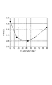
本実施形態に係る量子井戸構造の形成方法および半導体発光素子の製造方法により得られる効果について、従来の課題とともに説明する。ここで、比較のため、図7に従来の量子井戸構造の形成方法における(a)基板温度(炉内温度)の変化と、(b)原料ガス流量の変化とを示す。なお、図7(a),(b)に示す期間Tba〜Tbdはそれぞれ障壁層を成長させるための期間を示しており、期間Twa〜Twcはそれぞれ井戸層を成長させるための期間を示している。また、図7(b)において、グラフG4はGaの原料ガスであるTMGの流量を示しており、グラフG5はInの原料ガスであるTMIの流量を示しており、グラフG6はNの原料ガスであるNH3の流量を示している。図7に示した従来の方法において本実施形態の方法と異なる点は、井戸層を成長させる際(期間Twa〜Twc)に、TMI、TMG、およびNH3の供給を同時に開始している点である。 The effects obtained by the method for forming a quantum well structure and the method for manufacturing a semiconductor light emitting device according to this embodiment will be described together with conventional problems. Here, for comparison, FIG. 7 shows (a) a change in substrate temperature (furnace temperature) and (b) a change in raw material gas flow rate in a conventional method for forming a quantum well structure. In addition, periods Tb a to Tb d shown in FIGS. 7A and 7B indicate periods for growing the barrier layers, and periods Tw a to Tw c are periods for growing the well layers, respectively. Is shown. In FIG. 7B, a graph G4 shows the flow rate of TMG, which is a Ga source gas, a graph G5 shows a flow rate of TMI, which is an In source gas, and a graph G6 shows an N source gas. The flow rate of NH 3 is shown. The conventional method shown in FIG. 7 is different from the method of the present embodiment in that the supply of TMI, TMG, and NH 3 is started simultaneously when the well layer is grown (periods Tw a to Tw c ). Is a point.
本発明者らによる研究の結果、図7に示した従来の方法では、障壁層と井戸層との格子定数の相違に起因して、井戸層の成長初期においてIn組成が不十分となることがわかった。すなわち、InGaN井戸層の成長を開始した直後においてはGaN障壁層の直上にて十分なInの取り込みが行われず、井戸層の成長に従って徐々にIn組成が増大し、或る程度の厚さに達した時点で所望のIn組成が実現される。 As a result of the study by the present inventors, in the conventional method shown in FIG. 7, the In composition is insufficient at the early stage of the growth of the well layer due to the difference in the lattice constant between the barrier layer and the well layer. all right. That is, immediately after starting the growth of the InGaN well layer, sufficient In incorporation is not performed immediately above the GaN barrier layer, and the In composition gradually increases as the well layer grows, reaching a certain thickness. At that time, a desired In composition is realized.
ここで、図8(a)は、InGaNからなる井戸層の厚さと発光波長との理論上の相関を示すグラフである。同図のグラフG11に示すように、井戸層が厚くなるほど量子閉じ込め効果が小さくなり、発光波長は長波化する。また、同図のグラフG12に示すように、井戸幅が厚くなるほど膜厚方向にピエゾ電界が生じてバンドが曲がるので、井戸幅が厚くなるほど発光波長は長波化する。したがって、これらの作用を合成すると、井戸層の厚さと発光波長との理論上の相関は同図のグラフG13のようになり、井戸層が厚くなるほど発光波長が長くなると考えられる。 Here, FIG. 8A is a graph showing the theoretical correlation between the thickness of the well layer made of InGaN and the emission wavelength. As shown in the graph G11 in the figure, the thicker the well layer, the smaller the quantum confinement effect and the longer the emission wavelength. Further, as shown in the graph G12 of the same figure, as the well width increases, a piezo electric field is generated in the film thickness direction and the band bends. Therefore, the emission wavelength becomes longer as the well width increases. Therefore, when these actions are combined, the theoretical correlation between the thickness of the well layer and the emission wavelength is as shown in the graph G13 in the figure, and it is considered that the emission wavelength becomes longer as the well layer becomes thicker.
しかしながら、図7に示した従来の方法により作製した半導体発光素子の波長特性を調べた結果、図8(b)に示されるように、井戸層が薄い場合(図中の区間A)には発光波長が理論ほどには長波化しないことが判明した。このことからも、井戸層の成長初期においては十分なInの取り込みが行われず、In組成が不十分となることがわかる。 However, as a result of investigating the wavelength characteristics of the semiconductor light emitting device manufactured by the conventional method shown in FIG. 7, as shown in FIG. 8B, light is emitted when the well layer is thin (section A in the figure). It was found that the wavelength was not as long as the theory. This also indicates that sufficient In incorporation is not performed in the early stage of well layer growth, and the In composition becomes insufficient.
図9は、従来の方法により作製される量子井戸構造における(a)井戸層の厚さ方向位置とIn組成との関係、および(b)井戸層の厚さ方向位置とバンド構造との関係をそれぞれ示すグラフである。上述したように、InGaN井戸層の成長初期においてはIn組成が低くなり、InGaN井戸層の成長が進むにしたがって歪みが緩和されてIn組成が増大する傾向がある(図9(a))。特に、InGaN井戸層において成長面から2[nm]以下の範囲においては、In組成が低く抑えられる傾向がある。その結果、井戸層の層厚方向においてIn組成にばらつきが生じてしまうので、井戸層のバンド構造は図9(b)のようになり、発光波長の範囲が拡大して発光スペクトルの半値幅が大きくなってしまう。また、ヘテロ界面におけるバンドギャップ変化が緩くなってしまいキャリア閉じ込め作用が低下するといった問題や、発光に寄与する井戸層の体積が小さくなり発光強度が小さくなるといった問題も生じることとなる。 FIG. 9 shows (a) the relationship between the position in the thickness direction of the well layer and the In composition in the quantum well structure fabricated by the conventional method, and (b) the relationship between the position in the thickness direction of the well layer and the band structure. It is a graph shown, respectively. As described above, the In composition tends to be low at the initial stage of growth of the InGaN well layer, and the strain is relaxed and the In composition increases as the growth of the InGaN well layer proceeds (FIG. 9A). In particular, in the InGaN well layer, the In composition tends to be kept low in the range of 2 nm or less from the growth surface. As a result, the In composition varies in the thickness direction of the well layer, so that the band structure of the well layer is as shown in FIG. 9B, the range of emission wavelength is expanded, and the half width of the emission spectrum is increased. It gets bigger. In addition, the problem that the band gap change at the hetero interface becomes loose and the carrier confinement action is lowered, and the volume of the well layer that contributes to light emission is reduced and the light emission intensity is reduced.
そこで、本実施形態に係る量子井戸構造の形成方法および半導体発光素子の製造方法においては、InGaNからなる井戸層44,46,及び48を成長させる際、図6(b)に示したように、Ga原料ガス(TMG)の供給を開始する前に予めIn原料ガス(TMI)およびN原料ガス(NH3)を供給する。これにより、Ga原料ガス(TMG)の供給を開始するまでの期間Δtにおいて、In結晶およびInN結晶が障壁層43,45,及び47上に生成される。その後、Ga原料ガス(TMG)の供給を開始して井戸層44,46,及び48を引き続き成長させることによって、初期に形成されたIn結晶およびInN結晶が井戸層44,46,及び48に取り込まれ、井戸層44,46,及び48の成長初期におけるIn組成の低下を抑えることができる。したがって、井戸層44,46,及び48の層厚方向におけるIn組成のばらつきを抑えることができ、また井戸層44,46,及び48の厚さが例えば3[nm]といった薄い場合であっても所望のIn組成を実現できる。 Therefore, in the method for forming a quantum well structure and the method for manufacturing a semiconductor light emitting device according to this embodiment, when the well layers 44, 46, and 48 made of InGaN are grown, as shown in FIG. Before starting the supply of the Ga source gas (TMG), the In source gas (TMI) and the N source gas (NH 3 ) are supplied in advance. As a result, In crystal and InN crystal are generated on the barrier layers 43, 45, and 47 in the period Δt until the supply of Ga source gas (TMG) is started. Thereafter, the supply of Ga source gas (TMG) is started and the well layers 44, 46, and 48 are continuously grown, so that the initially formed In crystal and InN crystal are taken into the well layers 44, 46, and 48. Accordingly, it is possible to suppress a decrease in the In composition at the early stage of the growth of the well layers 44, 46, and 48. Therefore, variation in the In composition in the layer thickness direction of the well layers 44, 46, and 48 can be suppressed, and even when the thickness of the well layers 44, 46, and 48 is as thin as 3 nm, for example. A desired In composition can be realized.
図10は、本実施形態の方法により作製される量子井戸構造における(a)井戸層の厚さ方向位置とIn組成との関係、および(b)井戸層の厚さ方向位置とバンド構造との関係をそれぞれ示すグラフである。本実施形態の方法によれば、InGaN井戸層44,46,及び48の成長初期の段階で、障壁層43,45,及び47上においてInが過剰な状態を作り出すことができ、Inの取り込み量を改善できる。したがって、図10(a)に示すように層厚方向に均質なIn組成を有する井戸層を形成できるので、井戸層44,46,及び48のバンド構造は図10(b)のようになり、発光波長の拡がりを抑えて発光スペクトルの半値幅を狭くできる。更に、ヘテロ界面におけるバンドギャップ変化が急峻となるのでキャリア閉じ込め作用を高めることができ、また発光に寄与する井戸層44,46,及び48の体積が大きくなるので発光強度を強くできる。また、井戸層44,46,及び48のバンド構造が平坦であるほうが、量子閉じ込め作用による発光エネルギーの増加が抑えられるので、発光波長を長波化する作用もある。また、ピエゾ電界が層厚方向に均一に生じるので、ピエゾ効果がスクリーニングされないような小電流時の発光では波長が更に長くなると考えられる。 FIG. 10 shows (a) the relationship between the position in the thickness direction of the well layer and the In composition in the quantum well structure fabricated by the method of this embodiment, and (b) the position in the thickness direction of the well layer and the band structure. It is a graph which shows each relationship. According to the method of this embodiment, it is possible to create an excessive state of In on the barrier layers 43, 45, and 47 at the initial stage of growth of the InGaN well layers 44, 46, and 48, and the amount of In incorporation Can be improved. Therefore, since a well layer having a uniform In composition in the layer thickness direction can be formed as shown in FIG. 10A, the band structures of the well layers 44, 46, and 48 are as shown in FIG. The half-value width of the emission spectrum can be narrowed by suppressing the spread of the emission wavelength. Furthermore, since the band gap change at the hetero interface becomes steep, the carrier confinement effect can be enhanced, and the volume of the well layers 44, 46, and 48 contributing to light emission is increased, so that the light emission intensity can be increased. In addition, the flat band structure of the well layers 44, 46, and 48 can suppress an increase in emission energy due to the quantum confinement action, and thus has an action of increasing the emission wavelength. In addition, since the piezoelectric field is uniformly generated in the layer thickness direction, it is considered that the wavelength is further increased in light emission at a small current where the piezoelectric effect is not screened.
図11(a)は、図7に示した従来の方法により作製される量子井戸構造において、井戸層の目標In組成を例えば10%とした場合および30%とした場合のそれぞれにおける、井戸層の厚さ方向位置とIn組成との関係を示したグラフである。なお、この図11(a)において、グラフG21は井戸層の目標In組成を10%とした場合を示しており、グラフG22は井戸層の目標In組成を30%とした場合を示している。井戸層の厚さ方向位置に対するIn組成の変化率は互いに同様であるが、目標In組成が低い場合(グラフG21)には膜厚が薄い段階でIn組成が目標値に達することから、或る膜厚(例えば3[nm])の井戸層を成長させた場合におけるIn組成の層厚方向のばらつきは、目標In組成が大きい場合(グラフG22)の方が小さい場合(グラフG21)と比較して大きくなる。したがって、目標In組成が大きいほど、本実施形態の方法により得られる効果が顕著であるといえる。例えば、本実施形態のように、井戸層44,46,及び48の成長温度(第2の温度t2)を障壁層43,45,及び47の成長温度(第1の温度t1)より低くして井戸層44,46,及び48のIn組成を高めるような場合、層厚方向におけるIn組成のばらつきを特に効果的に抑えることができるので、例えば450[nm]以上650[nm]以下といった長いPL波長を有する井戸層を好適に形成できる。 FIG. 11A shows the well layer in the quantum well structure manufactured by the conventional method shown in FIG. 7 when the target In composition of the well layer is, for example, 10% and 30%. It is the graph which showed the relationship between thickness direction position and In composition. In FIG. 11A, graph G21 shows the case where the target In composition of the well layer is 10%, and graph G22 shows the case where the target In composition of the well layer is 30%. The rate of change of the In composition with respect to the position in the thickness direction of the well layer is similar to each other, but when the target In composition is low (graph G21), the In composition reaches the target value when the film thickness is small. The variation in the thickness direction of the In composition when a well layer having a film thickness (for example, 3 [nm]) is grown is compared with the case where the target In composition is larger (graph G22) and smaller (graph G21). Become bigger. Therefore, it can be said that the effect obtained by the method of the present embodiment is more remarkable as the target In composition is larger. For example, as in the present embodiment, the growth temperature (second temperature t 2 ) of the well layers 44, 46, and 48 is lower than the growth temperature (first temperature t 1 ) of the barrier layers 43, 45, and 47. In the case where the In composition of the well layers 44, 46, and 48 is increased, the variation of the In composition in the layer thickness direction can be particularly effectively suppressed. For example, 450 nm or more and 650 nm or less. A well layer having a long PL wavelength can be suitably formed.
また、図11(b)は、図7に示した従来の方法により作製される量子井戸構造において、障壁層がInGaNからなる場合(グラフG31)と、障壁層がGaNからなる場合(グラフG32)のそれぞれにおける、井戸層の厚さ方向位置とIn組成との関係を示したグラフである。図11(b)に示すように、障壁層がInGaNからなる場合(グラフG31)には、障壁層がGaNからなる場合(グラフG32)より膜厚が薄い段階でIn組成が増加し始める。したがって、障壁層がInGaNからなる場合と比較してGaNからなる場合のほうが層厚方向におけるIn組成のばらつきは大きくなるが、In組成を過大にすると井戸層と障壁層とのバンドギャップ差が小さくなり、量子井戸構造によるキャリア閉じ込め作用が低下してしまう。これに対し、本実施形態の方法によれば、障壁層がGaNからなる場合やInGaNからなりIn組成が小さい場合であっても、In組成のばらつきを効果的に抑制できるので、井戸層と障壁層とのバンドギャップ差を大きくしてキャリア閉じ込め作用を効果的に得ることができる。 FIG. 11B shows a case where the barrier layer is made of InGaN (graph G31) and the barrier layer is made of GaN (graph G32) in the quantum well structure manufactured by the conventional method shown in FIG. 5 is a graph showing the relationship between the position of the well layer in the thickness direction and the In composition. As shown in FIG. 11B, when the barrier layer is made of InGaN (graph G31), the In composition starts to increase at a stage where the film thickness is thinner than when the barrier layer is made of GaN (graph G32). Therefore, when the barrier layer is made of GaN, the variation in the In composition in the layer thickness direction is larger when the barrier layer is made of GaN. However, when the In composition is made excessive, the band gap difference between the well layer and the barrier layer is small. Thus, the carrier confinement effect due to the quantum well structure is reduced. On the other hand, according to the method of this embodiment, even when the barrier layer is made of GaN or when the In composition is made of InGaN and the In composition is small, variation in the In composition can be effectively suppressed. The band gap difference with the layer can be increased to effectively obtain the carrier confinement action.
図12は、図7に示した従来の方法により作製される量子井戸構造において、GaN基板のc面に対する主面の傾斜角(オフ角)が0°の場合(グラフG41)、15°または75°の場合(グラフG42)、30°または60°の場合(グラフG43)、及び45°の場合(グラフG44)のそれぞれにおける、井戸層の厚さ方向位置とIn組成との関係を示したグラフである。また、図13は、c面に対するオフ角と、InGaN結晶におけるIn組成比との関係を示すグラフである。図13に示すように、オフ角が0°の場合(すなわちc面を主面とするGaN基板上にInGaN結晶を成長させた場合)と比較して、オフ角が0°より大きい場合にはIn組成比が小さくなっており、オフ角が大きくなるほどInを取り込みにくくなる(In組成比がより小さくなる)傾向があることがわかる。したがって、図12に示すように、オフ角が45°に近いほど、膜厚が厚い段階(成長が進んだ段階)になるまでIn組成が増加せず、In組成のばらつきが大きくなる。 12 shows a quantum well structure manufactured by the conventional method shown in FIG. 7, when the inclination angle (off angle) of the main surface with respect to the c-plane of the GaN substrate is 0 ° (graph G41), 15 ° or 75 A graph showing the relationship between the position in the thickness direction of the well layer and the In composition in the case of ° (graph G42), 30 ° or 60 ° (graph G43), and 45 ° (graph G44). It is. FIG. 13 is a graph showing the relationship between the off angle with respect to the c-plane and the In composition ratio in the InGaN crystal. As shown in FIG. 13, when the off angle is larger than 0 ° as compared with the case where the off angle is 0 ° (that is, when the InGaN crystal is grown on the GaN substrate having the c-plane as the main surface). It can be seen that the In composition ratio is small, and that the In angle tends to be less likely to be taken in (the In composition ratio becomes smaller) as the off-angle increases. Therefore, as shown in FIG. 12, as the off angle is closer to 45 °, the In composition does not increase until the film thickness is thicker (the stage where growth has progressed), and the variation in In composition becomes larger.
本実施形態の方法は、このようにGaN基板のオフ角が大きくInを取り込みにくい場合に顕著な効果を発揮し、In組成のばらつきを効果的に抑制できる。すなわち、本実施形態のように、n型GaN基板40の主面はc面に対して傾斜していてもよい。井戸層44,46,及び48の発光波長を450[nm]以上650[nm]以下といった緑色から赤色の波長領域とする場合(特に、450[nm]以上550[nm]以下といった緑色の波長領域とする場合)、このようなオフ角を有するn型GaN基板40が用いられるが、本実施形態の方法によれば、このような場合にInの取り込み量を改善してIn組成のばらつきを効果的に抑えることができる。
The method of this embodiment exhibits a remarkable effect when the off-angle of the GaN substrate is large and it is difficult to capture In, and can effectively suppress variations in In composition. That is, as in this embodiment, the main surface of the n-
また、本実施形態のように、井戸層44,46,及び48のIn組成は15%以上であってもよい。このようにIn組成が比較的高い井戸層44,46,及び48を成長させる場合、従来は成長初期におけるInの取り込み量が少なく、所望のIn組成を得るために厚く成長させる必要があった。しかしながら、本実施形態の製造方法によれば、In組成が比較的高い井戸層44,46,及び48を成長させる場合であっても、例えば3[nm]といった薄い層厚でもって所望のIn組成を得ることができる。 Further, as in this embodiment, the In composition of the well layers 44, 46, and 48 may be 15% or more. Thus, when the well layers 44, 46, and 48 having a relatively high In composition are grown, conventionally, the amount of In taken in at the initial stage of growth is small, and it has been necessary to grow it thick in order to obtain a desired In composition. However, according to the manufacturing method of this embodiment, even when the well layers 44, 46, and 48 having a relatively high In composition are grown, a desired In composition with a thin layer thickness of, for example, 3 [nm] is used. Can be obtained.
また、本実施形態のように、井戸層44,46,及び48を成長させる際には、基板温度が第2の温度t2に達してからIn原料ガス(TMI)の供給を開始することが好ましい。これにより、井戸層44,46,及び48の成長初期においてIn結晶およびInN結晶を障壁層43,45,及び47上に効果的に生成し、上記した効果を好適に得ることができる。
Also, as in the present embodiment, when growing the
なお、本実施形態ではGa原料ガス(TMG)の供給を開始する前に、In原料ガス(TMI)とともにN原料ガス(NH3)を供給しているが、NH3の供給を停止してTMIのみ供給してもよい。この場合、TMGの供給を開始するまでの期間Δtにおいて、In結晶が障壁層43,45,及び47上に生成される。このような方法であっても、井戸層44,46,及び48の成長初期におけるIn組成の低下を効果的に抑えることができる。 In this embodiment, the N source gas (NH 3 ) is supplied together with the In source gas (TMI) before starting the supply of the Ga source gas (TMG), but the supply of NH 3 is stopped and the TMI is supplied. You may supply only. In this case, an In crystal is generated on the barrier layers 43, 45, and 47 in a period Δt until the supply of TMG is started. Even with such a method, it is possible to effectively suppress a decrease in the In composition at the early stage of the growth of the well layers 44, 46, and 48.
<実施例>
次に、高いIn組成の井戸層を有する緑色発光ダイオード構造を製造する方法の一実施例について説明する。
<Example>
Next, an embodiment of a method for manufacturing a green light emitting diode structure having a well layer with a high In composition will be described.
まず、c面に対しa軸方向に18°傾斜した主面を有するGaN基板(図3(a)のn型GaN基板40に相当)を反応炉内に設置し、反応炉内の圧力を27[kPa]としてNH3ガスおよびH2ガスを導入しつつ、炉内温度1050℃で10分間の熱処理を行う。その後、該反応炉内において基板温度を1150℃とし、TMGおよびNH3を導入するとともに、n型ドーパント源であるモノメチルシラン(MMSi)を導入することにより、n型のGaN層(図3(b)のn型GaN半導体層41に相当)を2[μm]の厚さに成長させる。
First, a GaN substrate (corresponding to the n-
続いて、基板温度を800℃まで下げ、TMG、TMI、NH3およびMMSiを反応炉内に導入してn型のInGaN緩衝層(図3(b)のn型InGaN緩衝層42に相当)を50[nm]の厚さに成長させる。この際、InGaN緩衝層のIn組成は5%とする。
Subsequently, the substrate temperature is lowered to 800 ° C., and TMG, TMI, NH 3 and MMSi are introduced into the reaction furnace to form an n-type InGaN buffer layer (corresponding to the n-type
続いて、基板温度を880℃(第1の温度t1)まで上げ、TMGおよびNH3を反応炉内に導入してInGaN緩衝層上にGaN障壁層(図4(a)に示した障壁層43に相当)を15[nm]の厚さに成長させる。そして、TMGの供給を一旦停止し、基板温度を700℃(第2の温度t2)まで下げ、TMI及びNH3(またはTMIのみ)を反応炉内に10秒間導入する。その後、TMGの供給も加えてIn0.30GaN井戸層(図4(b)に示した井戸層44に相当)を3[nm]の厚さに成長させる。以降、GaN障壁層およびIn0.30GaN井戸層の成長を上記と同様の方法により繰り返すことによって、3周期の多重量子井戸構造からなる活性層(図5(a)に示した活性層50に相当)を成長させる。なお、このときの基板温度および原料ガス流量の遷移は図6の通りである。
Subsequently, the substrate temperature is increased to 880 ° C. (first temperature t 1 ), TMG and NH 3 are introduced into the reaction furnace, and the GaN barrier layer (the barrier layer shown in FIG. 4A) is formed on the InGaN buffer layer. 43) is grown to a thickness of 15 [nm]. Then, the supply of TMG is temporarily stopped, the substrate temperature is lowered to 700 ° C. (second temperature t 2 ), and TMI and NH 3 (or only TMI) are introduced into the reaction furnace for 10 seconds. Thereafter, an In 0.30 GaN well layer (corresponding to the
続いて、TMGおよびTMIの供給を停止したのち基板温度を1000℃まで上昇させ、TMG、TMAおよびNH3を導入するとともに、p型ドーパント源であるビスシクロペンタジエニルマグネシウム(CP2Mg)を導入することにより、p型AlGaN層(図5(b)に示したp型AlGaN半導体層51に相当)を20[nm]の厚さに成長させる。そして、TMAの供給のみ停止し、p型GaN層(図5(b)のp型GaN半導体層52に相当)を50[nm]の厚さに成長させる。 Subsequently, after stopping the supply of TMG and TMI, the substrate temperature is raised to 1000 ° C., TMG, TMA and NH 3 are introduced, and biscyclopentadienyl magnesium (CP 2 Mg) which is a p-type dopant source is introduced. By introducing, a p-type AlGaN layer (corresponding to the p-type AlGaN semiconductor layer 51 shown in FIG. 5B) is grown to a thickness of 20 [nm]. Then, only the supply of TMA is stopped, and a p-type GaN layer (corresponding to the p-type GaN semiconductor layer 52 in FIG. 5B) is grown to a thickness of 50 [nm].
以上の工程により、高いIn組成の井戸層を有する緑色発光ダイオード構造を備えるエピタキシャルウェハが得られる。最後に、反応炉内の温度を室温まで下げてGaN基板を炉内から取り出したのち、図1の電極11及び19に相当する各電極を形成し、ウェハをチップ状に分割することにより、緑色発光ダイオードが得られる。
Through the above steps, an epitaxial wafer having a green light emitting diode structure having a well layer with a high In composition is obtained. Finally, the temperature in the reaction furnace is lowered to room temperature and the GaN substrate is taken out from the furnace. Then, each electrode corresponding to the
上記実施例により作製されたエピタキシャルウェハと、図7に示した方法により作製された従来のエピタキシャルウェハとの比較の為、これらのウェハの光励起による発光スペクトル及び電流注入による発光スペクトルについて計測した結果、上記実施例により作製されたウェハの方が、何れの発光スペクトルにおいてもその半値幅が狭く、また光強度も強くなった。また、発光波長は上記実施例により作製されたウェハの方が長かった。発光スペクトルの半値幅が狭いという結果は、井戸層を成長させる際、TMGの供給開始前に予めTMIを供給するによって、井戸層のIn組成の均一性が、厚さ方向及びウェハ面内の双方において向上したためと考えられる。また、発光強度が強くなったことに関しては、井戸層のIn組成の均一性が向上したことにより、井戸層と障壁層とのヘテロ界面におけるバンド構造が急峻となり、キャリア閉じ込め作用が強化されたためと考えられる。更に、発光波長が長くなったことに関しては、井戸層のIn組成の均一性が向上したことにより、井戸層と障壁層との格子定数差から生じるピエゾ電界が厚さ方向に均一となったためと考えられる。 For comparison between the epitaxial wafer produced by the above example and the conventional epitaxial wafer produced by the method shown in FIG. 7, as a result of measuring the emission spectrum by photoexcitation of these wafers and the emission spectrum by current injection, The wafer produced according to the above example had a narrower half-value width and higher light intensity in any emission spectrum. The emission wavelength of the wafer produced by the above example was longer. The result that the half-value width of the emission spectrum is narrow is that when the well layer is grown, the TMI is supplied in advance before starting the supply of TMG, so that the uniformity of the In composition of the well layer is improved both in the thickness direction and in the wafer surface. This is thought to be due to the improvement in Also, regarding the increase in emission intensity, the uniformity of the In composition of the well layer has improved, and the band structure at the heterointerface between the well layer and the barrier layer has become steep and the carrier confinement action has been enhanced. Conceivable. Furthermore, regarding the increase in the emission wavelength, the uniformity of the In composition of the well layer has improved, and the piezoelectric field resulting from the difference in lattice constant between the well layer and the barrier layer has become uniform in the thickness direction. Conceivable.
また、これらのウェハに対しX線回折測定を行ったところ、活性層の周期構造によるサテライトピークは、上記実施例により作製されたウェハの方がより急峻であった。このような現象も、井戸層と障壁層とのヘテロ界面におけるバンド構造が急峻となった結果といえる。 Further, when X-ray diffraction measurement was performed on these wafers, the satellite peak due to the periodic structure of the active layer was steeper in the wafer produced in the above example. This phenomenon is also a result of the steep band structure at the heterointerface between the well layer and the barrier layer.
本発明による量子井戸構造の形成方法、および半導体発光素子の製造方法は、上記した実施形態に限られるものではなく、他に様々な変形が可能である。例えば、上記実施形態においては、Inおよび他のIII族元素を有するIII族窒化物半導体からなる井戸層の例として、InGaNからなる井戸層を例示した。本発明における井戸層の構成材料はこれに限られず、Gaに代えて他のIII族元素を含んでもよく、或いはGaに加えて他のIII族元素を含んでもよい。また、活性層は、Nに加えて他のV族元素を更に含んでもよい。 The method of forming a quantum well structure and the method of manufacturing a semiconductor light emitting device according to the present invention are not limited to the above-described embodiments, and various other modifications are possible. For example, in the above embodiment, a well layer made of InGaN is exemplified as an example of a well layer made of a group III nitride semiconductor having In and other group III elements. The constituent material of the well layer in the present invention is not limited to this, and may contain other group III elements instead of Ga, or may contain other group III elements in addition to Ga. The active layer may further contain other group V elements in addition to N.
また、上記実施形態においては窒化ガリウム基板としてc面に対しオフ角を有するGaN基板を例示したが、c面を主面とするGaN基板を用いる場合においても本発明は上記実施形態と同種の効果を得ることができる。 In the above embodiment, a GaN substrate having an off-angle with respect to the c-plane is exemplified as the gallium nitride substrate. However, the present invention has the same effects as the above-described embodiment even when a GaN substrate having the c-plane as the main surface is used. Can be obtained.
1…半導体発光素子、3,41…n型GaN半導体層、5,50…活性層、5a,44,46,48…井戸層、5b,43,45,47,49…障壁層、7,51…p型AlGaN半導体層、9,52…p型GaN半導体層、11,19…電極、15,40…n型GaN基板、15a,40a…主面、21,42…n型InGaN緩衝層。
DESCRIPTION OF
Claims (12)
前記工程において、インジウムおよび他のIII族元素を有するIII族窒化物半導体を成長させることにより前記井戸層を形成し、
前記障壁層の成長温度を第1の温度とし、
前記井戸層の成長温度を前記第1の温度より低い第2の温度とし、
前記井戸層を成長させる際に、前記他のIII族元素の原料ガスの供給を開始する前に予めインジウムの原料ガスを供給し、その後インジウムの原料ガスの供給を停止することなく、前記他のIII族元素の原料ガスの供給を開始することを特徴とする、量子井戸構造の形成方法。
Forming a quantum well structure by alternately growing a barrier layer and a well layer on a main surface inclined with respect to the (0001) plane of the gallium nitride substrate;
In the step, the well layer is formed by growing a group III nitride semiconductor having indium and other group III elements,
The growth temperature of the barrier layer is a first temperature,
The growth temperature of the well layer is a second temperature lower than the first temperature,
When growing the well layer, supply the indium source gas in advance before starting the supply of the source gas of the other group III element , and then stop the supply of the indium source gas, A method for forming a quantum well structure, characterized by starting the supply of a source gas of a group III element .
窒化ガリウム基板の(0001)面に対して傾斜した主面上に障壁層および井戸層を交互に成長させることにより量子井戸活性層を形成する工程を備え、
前記工程において、インジウムおよび他のIII族元素を有するIII族窒化物半導体を成長させることにより前記井戸層を形成し、
前記障壁層の成長温度を第1の温度とし、
前記井戸層の成長温度を前記第1の温度より低い第2の温度とし、
前記井戸層を成長させる際に、前記他のIII族元素の原料ガスの供給を開始する前に予めインジウムの原料ガスを供給し、その後インジウムの原料ガスの供給を停止することなく、前記他のIII族元素の原料ガスの供給を開始することを特徴とする、半導体発光素子の製造方法。
A method for manufacturing a semiconductor light-emitting device having an emission wavelength of 450 [nm] or more and 650 [nm] or less,
Forming a quantum well active layer by alternately growing a barrier layer and a well layer on a main surface inclined with respect to the (0001) plane of the gallium nitride substrate;
In the step, the well layer is formed by growing a group III nitride semiconductor having indium and other group III elements,
The growth temperature of the barrier layer is a first temperature,
The growth temperature of the well layer is a second temperature lower than the first temperature,
When growing the well layer, supply the indium source gas in advance before starting the supply of the source gas of the other group III element , and then stop the supply of the indium source gas, A method for manufacturing a semiconductor light emitting device, comprising starting the supply of a group III element source gas .
Priority Applications (7)
| Application Number | Priority Date | Filing Date | Title |
|---|---|---|---|
| JP2008101781A JP4539752B2 (en) | 2008-04-09 | 2008-04-09 | Method for forming quantum well structure and method for manufacturing semiconductor light emitting device |
| TW098111047A TW200945452A (en) | 2008-04-09 | 2009-04-02 | Method for forming quantum well structure and method for manufacturing semiconductor light emitting element |
| US12/417,857 US8173458B2 (en) | 2008-04-09 | 2009-04-03 | Method for forming quantum well structure and method for manufacturing semiconductor light emitting element |
| EP09005065A EP2124266B1 (en) | 2008-04-09 | 2009-04-06 | Method for forming quantum well structure and method for manufacturing semiconductor light emitting element |
| AT09005065T ATE482475T1 (en) | 2008-04-09 | 2009-04-06 | METHOD FOR FORMING A QUANTUM WELL STRUCTURE AND METHOD FOR PRODUCING A LIGHT-EMITTING SEMICONDUCTOR ELEMENT |
| DE602009000219T DE602009000219D1 (en) | 2008-04-09 | 2009-04-06 | A method of forming a quantum well structure and a method of manufacturing a semiconductor light emitting element |
| CN200910134808.8A CN101556917B (en) | 2008-04-09 | 2009-04-09 | Method for forming quantum well structure and method for manufacturing semiconductor light emitting element |
Applications Claiming Priority (1)
| Application Number | Priority Date | Filing Date | Title |
|---|---|---|---|
| JP2008101781A JP4539752B2 (en) | 2008-04-09 | 2008-04-09 | Method for forming quantum well structure and method for manufacturing semiconductor light emitting device |
Publications (2)
| Publication Number | Publication Date |
|---|---|
| JP2009253164A JP2009253164A (en) | 2009-10-29 |
| JP4539752B2 true JP4539752B2 (en) | 2010-09-08 |
Family
ID=40911598
Family Applications (1)
| Application Number | Title | Priority Date | Filing Date |
|---|---|---|---|
| JP2008101781A Expired - Fee Related JP4539752B2 (en) | 2008-04-09 | 2008-04-09 | Method for forming quantum well structure and method for manufacturing semiconductor light emitting device |
Country Status (7)
| Country | Link |
|---|---|
| US (1) | US8173458B2 (en) |
| EP (1) | EP2124266B1 (en) |
| JP (1) | JP4539752B2 (en) |
| CN (1) | CN101556917B (en) |
| AT (1) | ATE482475T1 (en) |
| DE (1) | DE602009000219D1 (en) |
| TW (1) | TW200945452A (en) |
Families Citing this family (22)
| Publication number | Priority date | Publication date | Assignee | Title |
|---|---|---|---|---|
| TWI442455B (en) | 2010-03-29 | 2014-06-21 | Soitec Silicon On Insulator | Iii-v semiconductor structures and methods for forming the same |
| GB2487531A (en) * | 2011-01-20 | 2012-08-01 | Sharp Kk | Substrate system consisting of a metamorphic transition region comprising a laminate of AlxGa1-x N and the same material as the substrate. |
| WO2012098850A1 (en) | 2011-01-21 | 2012-07-26 | パナソニック株式会社 | Gallium nitride compound semiconductor light emitting element and light source provided with said light emitting element |
| CN102208500A (en) * | 2011-05-20 | 2011-10-05 | 武汉迪源光电科技有限公司 | Light-emitting diode (LED) epitaxial growth method and LED epitaxial structure |
| US20130023079A1 (en) * | 2011-07-20 | 2013-01-24 | Sang Won Kang | Fabrication of light emitting diodes (leds) using a degas process |
| WO2013046564A1 (en) | 2011-09-29 | 2013-04-04 | パナソニック株式会社 | Nitride semiconductor light emitting element and led system |
| JP5883331B2 (en) * | 2012-01-25 | 2016-03-15 | 住友化学株式会社 | Method of manufacturing nitride semiconductor epitaxial wafer and method of manufacturing field effect nitride transistor |
| WO2013132812A1 (en) | 2012-03-05 | 2013-09-12 | パナソニック株式会社 | Nitride semiconductor light-emitting element, light source, and method for manufacturing same |
| FR3001334B1 (en) * | 2013-01-24 | 2016-05-06 | Centre Nat De La Rech Scient (Cnrs) | PROCESS FOR PRODUCING MONOLITHIC WHITE DIODES |
| TWI612686B (en) * | 2014-09-03 | 2018-01-21 | 晶元光電股份有限公司 | Light-emitting device and manufacturing metode thereof |
| TWI714891B (en) * | 2014-09-03 | 2021-01-01 | 晶元光電股份有限公司 | Light-emitting device and manufacturing metode thereof |
| TWI641160B (en) * | 2014-09-03 | 2018-11-11 | 晶元光電股份有限公司 | Light-emitting device and manufacturing metode thereof |
| KR102238195B1 (en) | 2014-11-07 | 2021-04-07 | 엘지이노텍 주식회사 | Ultra violet light emitting device and lighting system |
| CN106972083B (en) * | 2017-02-17 | 2019-02-12 | 华灿光电(浙江)有限公司 | A kind of preparation method of the epitaxial wafer of light emitting diode |
| CN107634128A (en) * | 2017-09-14 | 2018-01-26 | 厦门三安光电有限公司 | Nitride semiconductor device |
| JP7095498B2 (en) * | 2018-08-31 | 2022-07-05 | 住友電気工業株式会社 | Method for manufacturing a vertical resonance type surface emitting laser and a vertical resonance type surface emitting laser |
| CZ2018563A3 (en) * | 2018-10-22 | 2019-10-30 | Fyzikální Ústav Av Čr, V. V. I. | Method of producing an epitaxial structure with InGaN quantum wells |
| CN113394313B (en) * | 2020-03-13 | 2022-12-27 | 华为技术有限公司 | LED chip, manufacturing method thereof, display module and terminal |
| CN113036600B (en) * | 2021-03-04 | 2022-08-02 | 东莞理工学院 | Gallium nitride-based green laser and preparation method thereof |
| CN113270525A (en) * | 2021-04-30 | 2021-08-17 | 广东德力光电有限公司 | Preparation method of green light epitaxial structure |
| CN114481088B (en) * | 2022-04-18 | 2022-07-01 | 苏州长光华芯光电技术股份有限公司 | Manufacturing method of superlattice active layer and semiconductor light-emitting structure |
| CN116344693B (en) * | 2023-05-31 | 2023-09-08 | 江西兆驰半导体有限公司 | High-light-efficiency light-emitting diode epitaxial wafer and preparation method thereof |
Citations (5)
| Publication number | Priority date | Publication date | Assignee | Title |
|---|---|---|---|---|
| JPH11168241A (en) * | 1997-12-04 | 1999-06-22 | Showa Denko Kk | Iii nitride semiconductor light emitting device |
| JP2001028458A (en) * | 1998-09-21 | 2001-01-30 | Nichia Chem Ind Ltd | Light emitting device |
| JP2002344089A (en) * | 2001-05-14 | 2002-11-29 | Sharp Corp | Nitride semiconductor light-emitting element and manufacturing method therefor |
| JP2003273470A (en) * | 2002-01-10 | 2003-09-26 | Sharp Corp | Iii-group nitride semiconductor laser element |
| JP2007515791A (en) * | 2004-08-13 | 2007-06-14 | ソウル ナショナル ユニヴァーシティー インダストリー ファンデーション | Method for growing nitride semiconductor layer and nitride semiconductor light emitting device using the same |
Family Cites Families (17)
| Publication number | Priority date | Publication date | Assignee | Title |
|---|---|---|---|---|
| WO1998019375A1 (en) | 1996-10-30 | 1998-05-07 | Hitachi, Ltd. | Optical information processor and semiconductor light emitting device suitable for the same |
| US6614059B1 (en) * | 1999-01-07 | 2003-09-02 | Matsushita Electric Industrial Co., Ltd. | Semiconductor light-emitting device with quantum well |
| JP4505915B2 (en) | 2000-01-13 | 2010-07-21 | 東京エレクトロン株式会社 | Deposition method |
| US6734530B2 (en) * | 2001-06-06 | 2004-05-11 | Matsushita Electric Industries Co., Ltd. | GaN-based compound semiconductor EPI-wafer and semiconductor element using the same |
| WO2002103812A1 (en) * | 2001-06-13 | 2002-12-27 | Matsushita Electric Industrial Co., Ltd. | Nitride semiconductor, production method therefor and nitride semiconductor element |
| US6645885B2 (en) | 2001-09-27 | 2003-11-11 | The National University Of Singapore | Forming indium nitride (InN) and indium gallium nitride (InGaN) quantum dots grown by metal-organic-vapor-phase-epitaxy (MOCVD) |
| GB2407701A (en) * | 2003-10-28 | 2005-05-04 | Sharp Kk | Manufacture of a semiconductor light-emitting device |
| TWI270217B (en) * | 2004-02-24 | 2007-01-01 | Showa Denko Kk | Gallium nitride-based compound semiconductor multilayer structure and production method thereof |
| JP2005268581A (en) * | 2004-03-19 | 2005-09-29 | Matsushita Electric Ind Co Ltd | Gallium nitride family compound semiconductor light emitting device |
| US7408199B2 (en) * | 2004-04-02 | 2008-08-05 | Nichia Corporation | Nitride semiconductor laser device and nitride semiconductor device |
| US7339255B2 (en) * | 2004-08-24 | 2008-03-04 | Kabushiki Kaisha Toshiba | Semiconductor device having bidirectionally inclined toward <1-100> and <11-20> relative to {0001} crystal planes |
| US20090200538A1 (en) * | 2004-09-28 | 2009-08-13 | Sumitomo Chemical Company, Limited | Group lll-V compound semiconductor and a method for producing the same |
| US20090140286A1 (en) | 2005-04-07 | 2009-06-04 | Showa Denko K.K. | Production Method of Group III Nitride Semiconductor Element |
| JP2006332258A (en) * | 2005-05-25 | 2006-12-07 | Matsushita Electric Ind Co Ltd | Nitride semiconductor device and its manufacturing method |
| JP2007087973A (en) | 2005-09-16 | 2007-04-05 | Rohm Co Ltd | Manufacture of nitride semiconductor device, method for manufacturing nitride semiconductor device, and nitride semiconductor light-emitting device obtained by the same |
| JP5896442B2 (en) * | 2006-01-20 | 2016-03-30 | 国立研究開発法人科学技術振興機構 | Group III nitride film growth method |
| JP5025168B2 (en) * | 2006-06-08 | 2012-09-12 | 昭和電工株式会社 | Method for producing group III nitride semiconductor multilayer structure |
-
2008
- 2008-04-09 JP JP2008101781A patent/JP4539752B2/en not_active Expired - Fee Related
-
2009
- 2009-04-02 TW TW098111047A patent/TW200945452A/en unknown
- 2009-04-03 US US12/417,857 patent/US8173458B2/en active Active
- 2009-04-06 DE DE602009000219T patent/DE602009000219D1/en active Active
- 2009-04-06 EP EP09005065A patent/EP2124266B1/en not_active Not-in-force
- 2009-04-06 AT AT09005065T patent/ATE482475T1/en not_active IP Right Cessation
- 2009-04-09 CN CN200910134808.8A patent/CN101556917B/en not_active Expired - Fee Related
Patent Citations (5)
| Publication number | Priority date | Publication date | Assignee | Title |
|---|---|---|---|---|
| JPH11168241A (en) * | 1997-12-04 | 1999-06-22 | Showa Denko Kk | Iii nitride semiconductor light emitting device |
| JP2001028458A (en) * | 1998-09-21 | 2001-01-30 | Nichia Chem Ind Ltd | Light emitting device |
| JP2002344089A (en) * | 2001-05-14 | 2002-11-29 | Sharp Corp | Nitride semiconductor light-emitting element and manufacturing method therefor |
| JP2003273470A (en) * | 2002-01-10 | 2003-09-26 | Sharp Corp | Iii-group nitride semiconductor laser element |
| JP2007515791A (en) * | 2004-08-13 | 2007-06-14 | ソウル ナショナル ユニヴァーシティー インダストリー ファンデーション | Method for growing nitride semiconductor layer and nitride semiconductor light emitting device using the same |
Also Published As
| Publication number | Publication date |
|---|---|
| EP2124266B1 (en) | 2010-09-22 |
| US8173458B2 (en) | 2012-05-08 |
| ATE482475T1 (en) | 2010-10-15 |
| CN101556917B (en) | 2013-01-09 |
| TW200945452A (en) | 2009-11-01 |
| CN101556917A (en) | 2009-10-14 |
| US20090258452A1 (en) | 2009-10-15 |
| DE602009000219D1 (en) | 2010-11-04 |
| EP2124266A1 (en) | 2009-11-25 |
| JP2009253164A (en) | 2009-10-29 |
Similar Documents
| Publication | Publication Date | Title |
|---|---|---|
| JP4539752B2 (en) | Method for forming quantum well structure and method for manufacturing semiconductor light emitting device | |
| JP5048236B2 (en) | Semiconductor light emitting device and method for manufacturing semiconductor light emitting device | |
| JP5108532B2 (en) | Nitride semiconductor light emitting device | |
| JP4888857B2 (en) | Group III nitride semiconductor thin film and group III nitride semiconductor light emitting device | |
| JP4999866B2 (en) | Method for growing gallium nitride based semiconductor heterostructure | |
| TWI381547B (en) | Light emitting device of iii-nitride based semiconductor and manufacturing method thereof | |
| EP2164115A1 (en) | Nitride semiconductor light emitting element and method for manufacturing nitride semiconductor | |
| WO2011125449A1 (en) | Nitrogen compound semiconductor light emitting element and manufacturing method thereof | |
| WO2015146069A1 (en) | Light emitting diode element | |
| JP2008288397A (en) | Semiconductor light-emitting apparatus | |
| JP2008103665A (en) | Nitride semiconductor device and its manufacturing method | |
| JP2009238772A (en) | Epitaxial substrate, and manufacturing method of epitaxial substrate | |
| JP2008028121A (en) | Manufacturing method of semiconductor luminescence element | |
| JP3626423B2 (en) | Photonic device manufacturing method | |
| JP2006100518A (en) | Method for treating surface of substrate and method for manufacturing group iii nitride compound semiconductor light-emitting element | |
| JP2009231609A (en) | Production method of semiconductor light-emitting element | |
| JP2008214132A (en) | Group iii nitride semiconductor thin film, group iii nitride semiconductor light-emitting element, and method for manufacturing group iii nitride semiconductor thin film | |
| JP2006128653A (en) | Group iii-v compound semiconductor, its manufacturing method and its use | |
| TW202123488A (en) | Led precursor incorporating strain relaxing structure | |
| JP2008227103A (en) | GaN-BASED SEMICONDUCTOR LIGHT EMITTING ELEMENT | |
| JP2011223043A (en) | Semiconductor light-emitting device and method of manufacturing the semiconductor light-emitting device | |
| KR20090107928A (en) | Method for forming quantum well structure and method for manufacturing semiconductor light emitting element | |
| KR102114619B1 (en) | Method for manufacturing non-polar nitride-based light emitting device | |
| JP4369970B2 (en) | Method for manufacturing compound semiconductor light emitting device and compound semiconductor light emitting device | |
| JP2007201152A5 (en) |
Legal Events
| Date | Code | Title | Description |
|---|---|---|---|
| A977 | Report on retrieval |
Free format text: JAPANESE INTERMEDIATE CODE: A971007 Effective date: 20100222 |
|
| A131 | Notification of reasons for refusal |
Free format text: JAPANESE INTERMEDIATE CODE: A131 Effective date: 20100309 |
|
| A521 | Request for written amendment filed |
Free format text: JAPANESE INTERMEDIATE CODE: A523 Effective date: 20100510 |
|
| TRDD | Decision of grant or rejection written | ||
| A01 | Written decision to grant a patent or to grant a registration (utility model) |
Free format text: JAPANESE INTERMEDIATE CODE: A01 Effective date: 20100601 |
|
| A01 | Written decision to grant a patent or to grant a registration (utility model) |
Free format text: JAPANESE INTERMEDIATE CODE: A01 |
|
| A61 | First payment of annual fees (during grant procedure) |
Free format text: JAPANESE INTERMEDIATE CODE: A61 Effective date: 20100614 |
|
| R150 | Certificate of patent or registration of utility model |
Free format text: JAPANESE INTERMEDIATE CODE: R150 |
|
| FPAY | Renewal fee payment (event date is renewal date of database) |
Free format text: PAYMENT UNTIL: 20130702 Year of fee payment: 3 |
|
| R250 | Receipt of annual fees |
Free format text: JAPANESE INTERMEDIATE CODE: R250 |
|
| LAPS | Cancellation because of no payment of annual fees |