JP4533582B2 - A CMOS compatible 3D image sensing system using quantum efficiency modulation - Google Patents
A CMOS compatible 3D image sensing system using quantum efficiency modulation Download PDFInfo
- Publication number
- JP4533582B2 JP4533582B2 JP2002550710A JP2002550710A JP4533582B2 JP 4533582 B2 JP4533582 B2 JP 4533582B2 JP 2002550710 A JP2002550710 A JP 2002550710A JP 2002550710 A JP2002550710 A JP 2002550710A JP 4533582 B2 JP4533582 B2 JP 4533582B2
- Authority
- JP
- Japan
- Prior art keywords
- semiconductor
- photodetector
- light energy
- integrated circuit
- photodetectors
- Prior art date
- Legal status (The legal status is an assumption and is not a legal conclusion. Google has not performed a legal analysis and makes no representation as to the accuracy of the status listed.)
- Expired - Lifetime
Links
- 238000000034 method Methods 0.000 claims abstract description 58
- 230000000737 periodic effect Effects 0.000 claims abstract description 32
- 238000012545 processing Methods 0.000 claims abstract description 25
- 230000008859 change Effects 0.000 claims abstract description 21
- 230000008569 process Effects 0.000 claims abstract description 7
- 230000003287 optical effect Effects 0.000 claims abstract description 6
- 239000004065 semiconductor Substances 0.000 claims abstract 84
- 239000000758 substrate Substances 0.000 claims description 34
- 230000010363 phase shift Effects 0.000 claims description 30
- 230000002441 reversible effect Effects 0.000 claims description 24
- 239000002019 doping agent Substances 0.000 claims description 23
- 230000008878 coupling Effects 0.000 claims description 4
- 238000010168 coupling process Methods 0.000 claims description 4
- 238000005859 coupling reaction Methods 0.000 claims description 4
- 230000001678 irradiating effect Effects 0.000 claims 2
- 238000001514 detection method Methods 0.000 abstract description 24
- 230000002123 temporal effect Effects 0.000 abstract description 12
- 230000000694 effects Effects 0.000 description 33
- 238000005259 measurement Methods 0.000 description 25
- 238000013459 approach Methods 0.000 description 17
- 239000003990 capacitor Substances 0.000 description 17
- 230000035945 sensitivity Effects 0.000 description 14
- 238000004519 manufacturing process Methods 0.000 description 11
- 230000006870 function Effects 0.000 description 10
- 238000006243 chemical reaction Methods 0.000 description 9
- 238000010586 diagram Methods 0.000 description 9
- 230000008901 benefit Effects 0.000 description 8
- 230000005540 biological transmission Effects 0.000 description 8
- 239000000463 material Substances 0.000 description 8
- 230000000295 complement effect Effects 0.000 description 7
- 230000005684 electric field Effects 0.000 description 7
- 238000005516 engineering process Methods 0.000 description 7
- 238000004364 calculation method Methods 0.000 description 6
- 238000009792 diffusion process Methods 0.000 description 6
- 238000003384 imaging method Methods 0.000 description 6
- 230000005855 radiation Effects 0.000 description 5
- 230000004044 response Effects 0.000 description 5
- XUIMIQQOPSSXEZ-UHFFFAOYSA-N Silicon Chemical compound [Si] XUIMIQQOPSSXEZ-UHFFFAOYSA-N 0.000 description 4
- 238000009825 accumulation Methods 0.000 description 4
- 238000004458 analytical method Methods 0.000 description 4
- 230000007423 decrease Effects 0.000 description 4
- 230000003071 parasitic effect Effects 0.000 description 4
- 229910052710 silicon Inorganic materials 0.000 description 4
- 239000010703 silicon Substances 0.000 description 4
- 238000012876 topography Methods 0.000 description 3
- 238000005513 bias potential Methods 0.000 description 2
- 238000001444 catalytic combustion detection Methods 0.000 description 2
- 238000004590 computer program Methods 0.000 description 2
- 230000003247 decreasing effect Effects 0.000 description 2
- 230000001934 delay Effects 0.000 description 2
- 238000013461 design Methods 0.000 description 2
- 230000005284 excitation Effects 0.000 description 2
- 238000001914 filtration Methods 0.000 description 2
- 238000005286 illumination Methods 0.000 description 2
- 230000007246 mechanism Effects 0.000 description 2
- 229910021420 polycrystalline silicon Inorganic materials 0.000 description 2
- 229920005591 polysilicon Polymers 0.000 description 2
- 238000003860 storage Methods 0.000 description 2
- 230000000007 visual effect Effects 0.000 description 2
- 229910000980 Aluminium gallium arsenide Inorganic materials 0.000 description 1
- 238000005481 NMR spectroscopy Methods 0.000 description 1
- 230000002411 adverse Effects 0.000 description 1
- 230000006399 behavior Effects 0.000 description 1
- 210000004556 brain Anatomy 0.000 description 1
- 238000013479 data entry Methods 0.000 description 1
- 230000003111 delayed effect Effects 0.000 description 1
- 230000006866 deterioration Effects 0.000 description 1
- 230000009977 dual effect Effects 0.000 description 1
- 230000012447 hatching Effects 0.000 description 1
- 230000010365 information processing Effects 0.000 description 1
- 230000003993 interaction Effects 0.000 description 1
- 238000013507 mapping Methods 0.000 description 1
- 238000012986 modification Methods 0.000 description 1
- 230000004048 modification Effects 0.000 description 1
- 230000006798 recombination Effects 0.000 description 1
- 238000005215 recombination Methods 0.000 description 1
- 238000012163 sequencing technique Methods 0.000 description 1
- 230000007704 transition Effects 0.000 description 1
- 210000001835 viscera Anatomy 0.000 description 1
- 238000003466 welding Methods 0.000 description 1
Images


Classifications
-
- G—PHYSICS
- G01—MEASURING; TESTING
- G01S—RADIO DIRECTION-FINDING; RADIO NAVIGATION; DETERMINING DISTANCE OR VELOCITY BY USE OF RADIO WAVES; LOCATING OR PRESENCE-DETECTING BY USE OF THE REFLECTION OR RERADIATION OF RADIO WAVES; ANALOGOUS ARRANGEMENTS USING OTHER WAVES
- G01S7/00—Details of systems according to groups G01S13/00, G01S15/00, G01S17/00
- G01S7/48—Details of systems according to groups G01S13/00, G01S15/00, G01S17/00 of systems according to group G01S17/00
- G01S7/491—Details of non-pulse systems
- G01S7/4912—Receivers
- G01S7/4915—Time delay measurement, e.g. operational details for pixel components; Phase measurement
-
- G—PHYSICS
- G01—MEASURING; TESTING
- G01S—RADIO DIRECTION-FINDING; RADIO NAVIGATION; DETERMINING DISTANCE OR VELOCITY BY USE OF RADIO WAVES; LOCATING OR PRESENCE-DETECTING BY USE OF THE REFLECTION OR RERADIATION OF RADIO WAVES; ANALOGOUS ARRANGEMENTS USING OTHER WAVES
- G01S17/00—Systems using the reflection or reradiation of electromagnetic waves other than radio waves, e.g. lidar systems
- G01S17/02—Systems using the reflection of electromagnetic waves other than radio waves
- G01S17/06—Systems determining position data of a target
- G01S17/08—Systems determining position data of a target for measuring distance only
- G01S17/32—Systems determining position data of a target for measuring distance only using transmission of continuous waves, whether amplitude-, frequency-, or phase-modulated, or unmodulated
- G01S17/36—Systems determining position data of a target for measuring distance only using transmission of continuous waves, whether amplitude-, frequency-, or phase-modulated, or unmodulated with phase comparison between the received signal and the contemporaneously transmitted signal
-
- G—PHYSICS
- G01—MEASURING; TESTING
- G01S—RADIO DIRECTION-FINDING; RADIO NAVIGATION; DETERMINING DISTANCE OR VELOCITY BY USE OF RADIO WAVES; LOCATING OR PRESENCE-DETECTING BY USE OF THE REFLECTION OR RERADIATION OF RADIO WAVES; ANALOGOUS ARRANGEMENTS USING OTHER WAVES
- G01S17/00—Systems using the reflection or reradiation of electromagnetic waves other than radio waves, e.g. lidar systems
- G01S17/88—Lidar systems specially adapted for specific applications
- G01S17/89—Lidar systems specially adapted for specific applications for mapping or imaging
- G01S17/894—3D imaging with simultaneous measurement of time-of-flight at a 2D array of receiver pixels, e.g. time-of-flight cameras or flash lidar
-
- G—PHYSICS
- G01—MEASURING; TESTING
- G01S—RADIO DIRECTION-FINDING; RADIO NAVIGATION; DETERMINING DISTANCE OR VELOCITY BY USE OF RADIO WAVES; LOCATING OR PRESENCE-DETECTING BY USE OF THE REFLECTION OR RERADIATION OF RADIO WAVES; ANALOGOUS ARRANGEMENTS USING OTHER WAVES
- G01S7/00—Details of systems according to groups G01S13/00, G01S15/00, G01S17/00
- G01S7/48—Details of systems according to groups G01S13/00, G01S15/00, G01S17/00 of systems according to group G01S17/00
- G01S7/491—Details of non-pulse systems
- G01S7/4912—Receivers
- G01S7/4913—Circuits for detection, sampling, integration or read-out
- G01S7/4914—Circuits for detection, sampling, integration or read-out of detector arrays, e.g. charge-transfer gates
-
- G—PHYSICS
- G01—MEASURING; TESTING
- G01S—RADIO DIRECTION-FINDING; RADIO NAVIGATION; DETERMINING DISTANCE OR VELOCITY BY USE OF RADIO WAVES; LOCATING OR PRESENCE-DETECTING BY USE OF THE REFLECTION OR RERADIATION OF RADIO WAVES; ANALOGOUS ARRANGEMENTS USING OTHER WAVES
- G01S7/00—Details of systems according to groups G01S13/00, G01S15/00, G01S17/00
- G01S7/48—Details of systems according to groups G01S13/00, G01S15/00, G01S17/00 of systems according to group G01S17/00
- G01S7/491—Details of non-pulse systems
- G01S7/493—Extracting wanted echo signals
-
- H—ELECTRICITY
- H01—ELECTRIC ELEMENTS
- H01L—SEMICONDUCTOR DEVICES NOT COVERED BY CLASS H10
- H01L27/00—Devices consisting of a plurality of semiconductor or other solid-state components formed in or on a common substrate
- H01L27/14—Devices consisting of a plurality of semiconductor or other solid-state components formed in or on a common substrate including semiconductor components sensitive to infrared radiation, light, electromagnetic radiation of shorter wavelength or corpuscular radiation and specially adapted either for the conversion of the energy of such radiation into electrical energy or for the control of electrical energy by such radiation
- H01L27/144—Devices controlled by radiation
- H01L27/146—Imager structures
- H01L27/14601—Structural or functional details thereof
- H01L27/14609—Pixel-elements with integrated switching, control, storage or amplification elements
-
- H—ELECTRICITY
- H01—ELECTRIC ELEMENTS
- H01L—SEMICONDUCTOR DEVICES NOT COVERED BY CLASS H10
- H01L27/00—Devices consisting of a plurality of semiconductor or other solid-state components formed in or on a common substrate
- H01L27/14—Devices consisting of a plurality of semiconductor or other solid-state components formed in or on a common substrate including semiconductor components sensitive to infrared radiation, light, electromagnetic radiation of shorter wavelength or corpuscular radiation and specially adapted either for the conversion of the energy of such radiation into electrical energy or for the control of electrical energy by such radiation
- H01L27/144—Devices controlled by radiation
- H01L27/146—Imager structures
- H01L27/14601—Structural or functional details thereof
- H01L27/14625—Optical elements or arrangements associated with the device
-
- H—ELECTRICITY
- H01—ELECTRIC ELEMENTS
- H01L—SEMICONDUCTOR DEVICES NOT COVERED BY CLASS H10
- H01L27/00—Devices consisting of a plurality of semiconductor or other solid-state components formed in or on a common substrate
- H01L27/14—Devices consisting of a plurality of semiconductor or other solid-state components formed in or on a common substrate including semiconductor components sensitive to infrared radiation, light, electromagnetic radiation of shorter wavelength or corpuscular radiation and specially adapted either for the conversion of the energy of such radiation into electrical energy or for the control of electrical energy by such radiation
- H01L27/144—Devices controlled by radiation
- H01L27/146—Imager structures
- H01L27/14643—Photodiode arrays; MOS imagers
Landscapes
- Engineering & Computer Science (AREA)
- Physics & Mathematics (AREA)
- General Physics & Mathematics (AREA)
- Electromagnetism (AREA)
- Radar, Positioning & Navigation (AREA)
- Remote Sensing (AREA)
- Computer Networks & Wireless Communication (AREA)
- Power Engineering (AREA)
- Condensed Matter Physics & Semiconductors (AREA)
- Computer Hardware Design (AREA)
- Microelectronics & Electronic Packaging (AREA)
- Optical Radar Systems And Details Thereof (AREA)
- Measurement Of Optical Distance (AREA)
- Length Measuring Devices By Optical Means (AREA)
Abstract
Description
(先行出願との関係)
出願人の2000年12月11日に出願された同時係属の米国特許仮出願シリアル番号60/254,873、「フォトダイオード量子効率変調を用いたCMOS 3Dマルチ画素センサー」より優先権を主張している。出願人は前記出願を参考し、ここに取り入れる。また、出願人は2001年6月6日に出願された同時係属の米国実用新案出願シリアル番号09/876,373、「削減されたピークエネルギーを用いたCMOSコンパチブルの三次元イメージセンシング」も参考し、ここに取り入れる。
(Relationship with prior application)
Claiming priority from applicant's co-pending US provisional patent
本発明は概してレンジファインダータイプのイメージセンサーに関係するもので、特に、CMOSファブリケーションを用いた一つの集積回路で実施可能なイメージセンサーに関する。更に詳しくは、そのようなセンサーを利用したシステムの消費電力を削減することに関する。 The present invention relates generally to a rangefinder type image sensor, and more particularly to an image sensor that can be implemented on a single integrated circuit using CMOS fabrication. More particularly, it relates to reducing power consumption of a system using such a sensor.
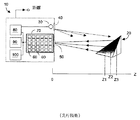
回路から対象物までの距離を測定する電子回路は当該技術においては知られており、図1のシステム10に例示することができる。図1の一般化されたシステムでは、システム10内のイメージング回路構成を用い、その最も上の部分がその最も下の部分より遠くに見せてある対象物20までのおよその距離(例えばZ1、Z2、Z3)を得る。一般的にシステム10は光源30を含み、光源30の光出力をレンズ40により集め、それを映される対象物、ここでは対象物20に導く。その他の従来技術のシステムは光源30を設けず、代わりに対象物が反射する周りの光に依存し、実際に周りの光を必要としている。
Electronic circuits that measure the distance from a circuit to an object are known in the art and can be illustrated in the
対象物20の表面部分が光源30からの光を様々な割合で反射し、レンズ50がこの光を集める。この戻り光が、例えば集積回路(IC)70上のアレイ内のフォトダイオードなどの様々な検出素子60に入射する。素子60は、この光景内の対象物(例えば10)の明度の解釈を提供し、そこから距離データを推定する。アプリケーションによっては、素子60が電荷結合されていたり(CCD)、CMOS素子のアレイであったりすることもある。
The surface portion of the
一般的にCCDは、第一のCCDで光検出した電荷を隣接するCCDに直列結合し、その出力を今度は第三のCCDに結合するというような、所謂バケツリレーの形で設定される。このバケツリレー設定は通常CCDアレイを含む同一のIC上に処理回路構成を製作することを妨げるものである。更に、CCDはランダム読み出しではなく直列的読み出しを提供する。例えば、CCDレンジファインダーシステムをデジタルズームレンズのアプリケーションに利用する場合、関係するデータのほとんどはアレイ中のほんの幾つかのCCDにより提供されるにもかかわらず、その関係するデータをアクセスするためにはアレイ全体を読み出す必要があり、そのプロセスは時間のかかるものである。静止画及びある種の動画アプリケーションにおいては、CCDに基づくシステムはまだ実用性があるかもしれない。 In general, the CCD is set in the form of a so-called bucket relay in which the charge detected by the first CCD is coupled in series to the adjacent CCD and the output is then coupled to the third CCD. This bucket relay setting normally prevents the fabrication of the processing circuit configuration on the same IC including the CCD array. In addition, CCDs provide serial readout rather than random readout. For example, when a CCD rangefinder system is utilized in a digital zoom lens application, an array is needed to access the relevant data, even though most of the relevant data is provided by only a few CCDs in the array. The whole needs to be read and the process is time consuming. For still images and some moving image applications, CCD based systems may still be practical.
記述したとおり、対象物20の上部は意図的にその下部よりも遠くに見せてある。つまり、距離Z3>Z2>Z1となっている。レンジファインダーのオートフォーカスのカメラ環境では、対象物から得られる相対的な明度データを検討することにより、カメラから(例えばZ=0から)対象物10までのおよその平均距離を素子60から得る。アプリケーションによっては、例えばレンジファインディング双眼鏡などでは、視野が極めて狭く、焦点を合わせた全ての対象物が実質的に同じ距離にある。しかし通常は、明度に基づくシステムはうまく働かない。例えば図1では、対象物20の上部はその下部よりもより暗く示されており、おそらくはその下部よりも更に遠く離れている。しかしながら現実の世界では、対象物のより遠く離れた部分はより近いがより暗い部分よりむしろ光沢があったり光輝いている(つまり、より多くの光エネルギーを反射して)こともある。複雑なシーンでは、背景をバックに立っている対象物または被写体までの焦点距離を、被写体を背景から識別するために明度の変化を用いて概算することは大変困難である。そのような様々なアプリケーションにおいては、図1のシステム10内の回路80、回路90及び回路100がこの信号処理を補助する。記述したとおり、IC70がCCD60を含む場合、回路80、回路90及び回路100などのその他の回路はチップ外に製作される。
As described, the upper part of the
対象物の反射率が不明なので、反射された明度のデータは残念ながら距離の本当に正確な解釈を提供するわけではない。したがって、遠く離れた対象物表面の光る表面は、近くの対象物の光沢のない表面と同じだけの(おそらくはそれ以上の)光を反射することもある。 Since the reflectance of the object is unknown, the reflected brightness data unfortunately does not provide a truly accurate interpretation of distance. Thus, the shiny surface of a remote object surface may reflect as much (possibly more) light than the matte surface of a nearby object.
当該技術においてはその他のフォーカスシステムが知られている。カメラや双眼鏡に用いられる赤外線(IR)オートフォーカスシステムは、視野内の全てのターゲットまでの平均距離もしくは最短距離である一つの距離を出す。その他のカメラのオートフォーカスシステムでは、距離を測定するためにレンズを被写体に機械的にフォーカスすることがしばしば必要となる。これらの従来技術のフォーカスシステムは、レンズを視野内の一つの対象物に合わせるのがせいぜいで、視野内の全ての対象物の距離を同時に測ることはできない。 Other focus systems are known in the art. Infrared (IR) autofocus systems used in cameras and binoculars produce a single distance that is the average or shortest distance to all targets in the field of view. In other camera autofocus systems, it is often necessary to mechanically focus the lens on the subject in order to measure distance. These prior art focusing systems cannot at the same time measure the distances of all objects in the field of view, at best, with the lens set to one object in the field of view.
一般的に、シーンにおける元の明度の再生や概算によって、人間の視覚システムがそのシーンにおいてどの対象物が存在したかを理解し、またそれらの相対的位置を両眼的に推定することが可能になる。普通のテレビ画面に映し出されたような悲両眼的なイメージについては、人間の脳は過去の経験を用いて対象物の外見上の大きさ、距離及び形を見極める。専門のコンピュータプログラムによって特別な条件下における対象物の距離を概算することもできる。 In general, by reproducing and approximating the original brightness in a scene, the human visual system can understand what objects were present in the scene and estimate their relative positions binocularly become. For a binocular image as projected on an ordinary television screen, the human brain uses past experience to determine the apparent size, distance and shape of the object. A specialized computer program can also estimate the distance of an object under special conditions.
両眼的なイメージによって観測者はより正確に対象物の距離を判断することができる。しかしながら、コンピュータプログラムが両眼的イメージから対象物の距離を判断するのは難しい。しばしばエラーが発生し、必須信号処理には専門のハードウェアと計算が必要となる。両眼的イメージは、せいぜい直接コンピュータに使用するのに適した三次元イメージを作り出す間接的な方法といったところである。 The binocular image allows the observer to more accurately determine the distance of the object. However, it is difficult for a computer program to determine the distance of an object from a binocular image. Errors often occur and essential signal processing requires specialized hardware and computation. Binocular images are at best an indirect way of creating a three-dimensional image suitable for direct computer use.
多くのアプリケーションでは、シーンの三次元的解釈を直接得ることが必要である。しかし実際には、明度測定から視線軸に沿って距離と速度のデータを正確に抽出することは困難である。それでもなお、多くのアプリケーションにおいて距離と速度の正確な追跡が要求されている。例えば、組み立てラインの溶接ロボットは溶接する対象物の正確な距離と速度を測定しなければならない。必要とされる距離の測定は変化する照明条件や上述したその他の欠点により誤ったものになることもある。三次元イメージを直接捕らえることが可能なシステムはそのようなアプリケーションに恩恵をもたらすものである。 In many applications it is necessary to obtain a three-dimensional interpretation of the scene directly. However, in practice, it is difficult to accurately extract distance and velocity data along the visual axis from the brightness measurement. Nevertheless, accurate tracking of distance and speed is required in many applications. For example, an assembly line welding robot must measure the exact distance and speed of objects to be welded. The required distance measurement may be incorrect due to changing lighting conditions and other drawbacks mentioned above. Systems that can directly capture 3D images can benefit such applications.
専門の三次元イメージングシステムは、核磁気共振と走査型レーザーの分野では存在するものの、そのようなシステムは相当の設備費がかかる。更に、これらのシステムはひどく邪魔なもので、また、例えば体内の臓器を映し出すなどの特定の仕事専用のものである。 Although specialized three-dimensional imaging systems exist in the field of nuclear magnetic resonance and scanning lasers, such systems require considerable equipment costs. In addition, these systems are terribly disturbing and are dedicated to specific tasks, such as projecting internal organs.
その他のアプリケーションでは、走査型レーザー式レンジファインディングシステムで、x軸面とおそらくはy軸面においてもレーザー光線を屈折させるミラーを用いて、イメージをラスター走査する。各ミラーの曲角度は、サンプリングするイメージ画素の座標を決定するために使われる。このようなシステムでは、どの画素を見ているのかを知るために各ミラーの角度を正確に検出する必要がある。当然のことながら、精密可動機械部品を提供しなければならないということは、そのようなレンジファインディングシステムをより大きく、複雑で、コストのかかるものにしている。更に、このようなシステムは各画素を直列的にサンプリングするため、単位時間毎にサンプリングできる完全なイメージフレームの数は限られている。「画素」という用語は検出器のアレイ中の一つ以上の検出器によって出された出力結果を指すものとする。 In other applications, a scanning laser range finding system raster scans an image using a mirror that refracts the laser beam also in the x-axis plane and possibly the y-axis plane. The angle of curvature of each mirror is used to determine the coordinates of the image pixel to be sampled. In such a system, it is necessary to accurately detect the angle of each mirror in order to know which pixel is being viewed. Of course, the need to provide precision moving mechanical parts makes such a range finding system larger, more complex and costly. Furthermore, since such a system samples each pixel in series, the number of complete image frames that can be sampled per unit time is limited. The term “pixel” shall refer to an output result produced by one or more detectors in an array of detectors.
まとめると、好ましくは一つのIC上にCMOSファブリケーション技術を用いて、必要とする個別の部品の数が少なく、可動部品を全く必要としない直接三次元イメージングを行えるシステムが求められている。オプションとして、システムは非直列的またはランダムに検出器からのデータを出力できる。より好ましくは、そのようなシステムは、必要とするピーク発光出力が比較的低く安価な発光体を用いることもでき、しかしながら高い感度を提供する。
本発明はそのようなシステムを提供するものである。
In summary, there is a need for a system that can perform direct three-dimensional imaging, preferably using CMOS fabrication technology on a single IC, requiring fewer individual parts and requiring no moving parts. Optionally, the system can output data from the detector non-serially or randomly. More preferably, such a system can also use an inexpensive illuminant that requires a relatively low peak light output, but provides high sensitivity.
The present invention provides such a system.
本発明は、明度のデータに依存するのではなく飛行時間(TOF)データを用いてリアルタイムで距離と速度のデータを測るシステムを提供するものである。本システムはCMOSコンパチブルであり、可動部品を必要とすることなくこうした三次元イメージングを提供する。本システムは、フォトン光エネルギーを検出するCMOSコンパチブルの画素検出器と関連する処理回路構成の両方を含む一つのIC上に製作することができる。 The present invention provides a system for measuring distance and speed data in real time using time-of-flight (TOF) data rather than relying on brightness data. The system is CMOS compatible and provides such 3D imaging without the need for moving parts. The system can be fabricated on a single IC that includes both a CMOS compatible pixel detector that detects photon light energy and associated processing circuitry.
出願人の米国特許6,323,942B1(2001)、「CMOSコンパチブルな三次元イメージセンサーIC」では、CMOSコンパチブルのIC上のマイクロプロセッサーが好ましくはLEDまたはレーザー光供給源を連続的にトリガーし、イメージングする対象物の表面上の点が少なくとも部分的に光出力パルスを反射する。例えばcmなどの良好なイメージ解像度を得るには、光エネルギーの大きくしかし短いパルスが必要とされる。例えば、10Wのピークパルスエネルギー、約15nsのパルス幅、そして約3KHZの繰り返し周波数といった具合である。出願人の先のシステムの平均エネルギーは僅か1mWであるのに対し、10Wのピーク電力が求められるということは、好ましいエネルギー光源として比較的高価なレーザーダイオードの使用を本質的に決定づけることになる。検出器アレイの各画素検出器は、光エネルギーパルスの発信からリターン信号の検出までの飛行時間を測る関連エレクトロニクスを有する。該発明では、高ピーク電力狭エネルギーパルスの発信に高バンド幅画素検出器増幅器が必要である。 In Applicant's US Pat. No. 6,323,942B1 (2001), “CMOS-compatible three-dimensional image sensor IC”, a microprocessor on a CMOS-compatible IC preferably triggers an LED or laser light source continuously, A point on the surface of the object to be imaged at least partially reflects the light output pulse. To obtain a good image resolution, eg cm, a large but short pulse of light energy is required. For example, a peak pulse energy of 10 W, a pulse width of about 15 ns, and a repetition frequency of about 3 KHZ. The average energy of Applicant's previous system is only 1 mW, whereas the requirement of 10 W peak power essentially dictates the use of a relatively expensive laser diode as the preferred energy source. Each pixel detector of the detector array has associated electronics that measure the time of flight from the transmission of the light energy pulse to the detection of the return signal. The invention requires a high bandwidth pixel detector amplifier for the transmission of high peak power narrow energy pulses.
参照されている出願人の同時係属の米国特許出願は、小さな平均電力と何Wではなく数十mWといったと小さなピーク電力の高周波数成分を持つ周期的信号を送信するシステムを開示する。解析を簡単にするために、cos(ω・t)などの理想的な正弦波波形の光エネルギーの周期的信号を仮定したが、ここでもそう仮定する。こうした低ピーク電力の高周波数成分の周期的信号を放射することにより、安価な光源や簡単な狭バンド幅の画素検出器を利用することができる。約200MHzの動作(放射エネルギー変調)周波数に対し、バンド幅は数百KHzの桁でよい。良好な解像精度が、低ピーク電力の発光器を利用しても得られるが、これは狭パルスの高ピーク電力の発光器からの出力よりも有効繰り返し周波数が高いということである。 The referenced Applicant's co-pending US patent application discloses a system that transmits a periodic signal with a small average power and a high frequency component with a small peak power, such as several tens of milliwatts rather than several watts. In order to simplify the analysis, a periodic signal of light energy having an ideal sinusoidal waveform such as cos (ω · t) is assumed, but this is also assumed here. By emitting a periodic signal having such a low peak power and a high frequency component, an inexpensive light source and a simple narrow bandwidth pixel detector can be used. For an operating (radiant energy modulation) frequency of about 200 MHz, the bandwidth may be on the order of several hundred KHz. Good resolution accuracy can also be obtained using low peak power light emitters, which have a higher effective repetition rate than the output from narrow pulse high peak power light emitters.
このようなシステムにおいて、及び本発明において、光源から放射されたエネルギーがおよそS1=K・cos(ω・t)であってKが振幅係数で、ω=2πfであり、周波数fはおそらく200MHZであるとする。更に、光エネルギー発光器とターゲット対象物とを隔てる距離がzであるとする。数学的に分かり易く表現するために、K=1とするが、1以下または1以上の係数を使ってもよい。「およそ」という言葉は完全な正弦波の波形を発生することは困難であるという認識のもとに使われている。エネルギーが距離zを横断するために必要な飛行時間のために、発信されたエネルギーとアレイ中の光検出器で検出されたエネルギーの間に、S2=A・cos(ω・t+φ)という位相シフトφがある。係数Aは検出された反射された信号の輝度を表し、画素検出器が受信した同一の帰還信号を用いて別途測ることができる。 In such a system, and in the present invention, the energy emitted from the light source is approximately S 1 = K · cos (ω · t), K is the amplitude coefficient, ω = 2πf, and the frequency f is probably 200 MHZ. Suppose that Further, assume that the distance separating the light energy emitter and the target object is z. In order to express mathematically easily, K = 1, but a coefficient of 1 or less or 1 or more may be used. The term “approximately” is used with the recognition that it is difficult to generate a complete sinusoidal waveform. Because of the time of flight required for the energy to traverse the distance z, the phase S 2 = A · cos (ω · t + φ) between the transmitted energy and the energy detected by the photodetectors in the array There is a shift φ. The coefficient A represents the brightness of the detected reflected signal and can be measured separately using the same feedback signal received by the pixel detector.
飛行時間による位相シフトφは:
Φ=2・ω・z/C=2・(2・π・f)・z/C
となる。ここでCは光の速度300,000Km/秒である。したがって、エネルギー発光器から(及び検出器アレイから)の距離zは次のように求められる:
z=Φ・C/2・ω=ΦC/{2・(2・π・f)}
The phase shift φ by time of flight is:
Φ = 2 · ω · z / C = 2 · (2 · π · f) · z / C
It becomes. Here, C is the speed of light of 300,000 Km / sec. Thus, the distance z from the energy emitter (and from the detector array) is determined as follows:
z = Φ · C / 2 · ω = ΦC / {2 · (2 · π · f)}
距離zは2πC/(2・ω)=C/(2・f)をモジュロとして得られる。必要に応じて、f1、f2、f3、....といった光放射エネルギーの幾つかの異なる変調周波数を用いて、C/(2・f1)、C/(2・f2)、C/(2・f3)をモジュロとしてzを測定してもよい。複数の異なる変調周波数を使用することは、エイリアシングを減らす効果がある。仮にf1、f2、f3が整数であるとすると、エイリアシングはLCM(f1、f2、f3)と表されるf1、f2、f3の最小公倍数にまで減らされる。f1、f2、f3が整数でない場合は、a1/D、a2/D、a3/Dと表現できる分数にモデル化することが好ましい。ここでaiのiは整数で、D=(GCD)はa1、a2、a3の最大公約数を表す。上記から距離zは、LCM(a1、a2、a3)/Dをモジュロとして決定することができる。これと同様の分析的アプローチは、ここに後述する本発明の様々な実施例においても実施される。 The distance z is obtained modulo 2πC / (2 · ω) = C / (2 · f). If necessary, f 1 , f 2 , f 3 ,. . . . Z can be measured using C / (2 · f 1 ), C / (2 · f 2 ), and C / (2 · f 3 ) as modulo using several different modulation frequencies of light radiation energy such as Good. Using a plurality of different modulation frequencies has the effect of reducing aliasing. If f 1 , f 2 , and f 3 are integers, aliasing is reduced to the least common multiple of f 1 , f 2 , and f 3 expressed as LCM (f 1 , f 2 , f 3 ). When f 1 , f 2 , and f 3 are not integers, it is preferable to model into fractions that can be expressed as a 1 / D, a 2 / D, and a 3 / D. Here, i of a i is an integer, and D = (GCD) represents the greatest common divisor of a 1 , a 2 , and a 3 . From the above, the distance z can be determined by using LCM (a 1 , a 2 , a 3 ) / D as modulo. A similar analytical approach is implemented in the various embodiments of the invention described herein below.
位相Φと距離zは、各画素検出器が検出する信号S2=A・cos(ω・t+Φ)と光エネルギー発光器を駆動する信号S1=cos(ω・t)とを混合する(またはホモダイン受信する)ことにより測定できる。混合した結果S1・S2は、0.5・A・{cos(2・ω・t+Φ)+cos(Φ)}となり、時間平均値は0.5・A・cos(Φ)となる。必要に応じて、検出された帰還信号の振幅つまり輝度Aを別途各画素検出器出力から測ってもよい。 The phase Φ and the distance z mix the signal S 2 = A · cos (ω · t + Φ) detected by each pixel detector and the signal S 1 = cos (ω · t) that drives the light energy emitter (or It can be measured by receiving homodyne. The mixed result S 1 · S 2 is 0.5 · A · {cos (2 · ω · t + Φ) + cos (Φ)}, and the time average value is 0.5 · A · cos (Φ). If necessary, the amplitude of the detected feedback signal, that is, the luminance A may be separately measured from the output of each pixel detector.
位相Φと距離zのホモダイン測定を実施するには、検出器アレイ中の各画素検出器が、関連する画素検出器が検出した信号を増幅する低ノイズ増幅器、可変位相遅延ユニット、ミキサー、ローパスフィルター及び積分器を含む専用のエレクトロニクスを有する。ミキサーは低ノイズ増幅器の出力を発信された正弦波信号を可変位相遅延したものと混合する。ミキサーの出力はローパスフィルターで処理され、積分されて、可変位相遅延ユニットのコントロール位相シフトにフィードバックされる。平衡状態において各積分器の出力は、関連する画素検出器と距離z離れているターゲット対象物上の点との間の飛行時間TOFつまり距離zに関連する位相Ψ(Ψ=Φ±π/2とする)となる。アナログ位相情報は直ちにデジタル変換され、チップ上のマイクロプロセッサーはそこで各画素検出器から関連するターゲット対象物上の点までのzの値を計算できる。必要に応じて、マイクロプロセッサーは更にdz/dt(及び/またはdx/dt、dy/dt)も計算できる。 To perform homodyne measurement of phase Φ and distance z, each pixel detector in the detector array amplifies the signal detected by the associated pixel detector, a low noise amplifier, a variable phase delay unit, a mixer, a low pass filter And dedicated electronics including an integrator. The mixer mixes the sinusoidal signal transmitted from the output of the low noise amplifier with a variable phase delayed signal. The output of the mixer is processed by a low-pass filter, integrated, and fed back to the control phase shift of the variable phase delay unit. In equilibrium, the output of each integrator is the time of flight TOF between the associated pixel detector and a point on the target object that is a distance z or the phase Ψ (Ψ = Φ ± π / 2) related to the distance z. And). The analog phase information is immediately digitized and the microprocessor on the chip can then calculate the value of z from each pixel detector to a point on the associated target object. If necessary, the microprocessor can also calculate dz / dt (and / or dx / dt, dy / dt).
しかしながら、出願人が参考とした同時係属の特許仮出願では、低ピーク電力高周波数成分の周期的信号を用い、位相遅延を利用してTOF、dz/dt(及び/またはdx/dt、dy/dt)及びその他の情報を測定する、こうしたシステムの検出感度が相当に高められている。より詳しくは、改善されたミキサーについての記述があり、その中で混合は、例えばMOSトランジスターのゲートの使用や光検出器の逆バイアスの変更により検出器アレイ中の光検出器の量子効率(QE)を変調した結果として行われている。そのような混合のもたらす効果としては高周波感度の改善、検出信号/ノイズ比の改善、より小さなフォームファクター、電力消費の減少及び製作コストの削減などがある。 However, in the co-pending patent provisional application referred to by the applicant, a periodic signal having a low peak power and a high frequency component is used, and phase delay is used to make TOF, dz / dt (and / or dx / dt, dy / The detection sensitivity of such systems measuring dt) and other information is considerably increased. More specifically, there is a description of an improved mixer, in which mixing is performed, for example, by using the gate of a MOS transistor or by changing the reverse bias of the photodetector, the quantum efficiency (QE) of the photodetector in the detector array. ) As a result of modulation. Such mixing effects include improved high frequency sensitivity, improved detection signal / noise ratio, smaller form factor, reduced power consumption, and reduced manufacturing costs.
本発明では、QE変調の実施例を幾つか記載する。概念的にはそれらの実施例は二つの一般的なカテゴリーに分類できる。最初のカテゴリーは可変位相遅延アプローチ(出願人の同時係属出願シリアル番号09/876,373に記載されたものと似ていなくはないもの)に関係するもので、ただし専用エレクトロニックミキサー(例えばギルバートセルなど)がQE変調で置き換えているものである。2番目のカテゴリーはQE変調を用いて固定位相で混合し、様々な空間的マルチプレクシングアプローチ及び時間的マルチプレクシングアプローチの実施に関わるものである。どちらの方法も、フォトダイオードの逆バイアスを変更することにより、またはMOSで実施したフォトゲート付きのフォトダイオードにゲート電圧を加えた後変更することにより、MOSで実施したフォトダイオードのQEを変調する効果がある。どちらの方法にも、シングルエンドまたはダブルエンドの差動信号処理を用いてもよい。差動QE変調は、より迅速なQE変調が可能になるという効果があり、かつ環境光やフォトダイオードの暗電流による共通モード効果を十分に除去する差動出力を提供する。一般的に、どちらの方法のカテゴリーも、フォトダイオードのキャパシターに光検出器信号電荷を蓄積するために有利である。必要に応じて、QE変調停止時に蓄積された電荷を周期的に調べてもよい。そのような信号蓄積アプローチは、高周波数で小振幅の光電流を直接測ろうとする方法よりも好ましい。 In the present invention, several examples of QE modulation are described. Conceptually, these embodiments can be divided into two general categories. The first category relates to variable phase delay approaches (those not similar to those described in Applicant's co-pending application serial number 09 / 876,373), but dedicated electronic mixers (eg Gilbert cell etc.) ) Is replaced by QE modulation. The second category mixes with fixed phase using QE modulation and involves the implementation of various spatial and temporal multiplexing approaches. Both methods modulate the QE of a photodiode implemented in MOS by changing the reverse bias of the photodiode or by changing the gate voltage after applying the gate voltage to a photodiode with a photogate implemented in MOS. effective. Either method may use single-ended or double-ended differential signal processing. The differential QE modulation has an effect of enabling a quicker QE modulation, and provides a differential output that sufficiently eliminates a common mode effect caused by ambient light or a dark current of a photodiode. In general, both method categories are advantageous for storing photodetector signal charge in a photodiode capacitor. If necessary, the charge accumulated when QE modulation is stopped may be periodically checked. Such a signal storage approach is preferred over methods that attempt to directly measure high frequency and small amplitude photocurrents.
可変位相遅延(カテゴリー1)を用いて、QE変調された画素フォトダイオード(またはフォトゲートフォトダイオード)それぞれからの光電流を、広バンド幅、高周波数応答または高閉ループ利得を示す必要のない、関連する比較的高入力のインピーダンス増幅器に入力として結合する。増幅器の出力はローパスフィルター(LPF)に直接加えられ、このLPFの出力が積分器を駆動する。積分器の出力を、光検出器ダイオードを駆動するQE変調信号をコントロールする可変位相遅延(VPD)をコントロールするように結合する。VPDもまた光エネルギー発光器をコントロールする周期的信号ジェネレーターからの信号により駆動される。画素フォトダイオード検出器からの出力信号及びホモダイン駆動信号に関連するDCオフセットがあってもなくてもよい。オフセットがないと想定して、定常状態においてLPF出力はゼロとなる。適当なDCオフセットがあるものと想定すると、定常状態においてLPF出力は最小値または最大値となる。この方法はシングルエンドで実施してもよいが、ポジティブ信号とネガティブ信号をQE変調され位相の揃っていないフォトダイオードから得る、相補型アプローチを用いてダブルエンドで実施する方が好ましい。 Using variable phase delay (category 1), the photocurrent from each QE modulated pixel photodiode (or photogate photodiode) does not need to exhibit wide bandwidth, high frequency response or high closed loop gain Coupled as an input to a relatively high input impedance amplifier. The output of the amplifier is directly applied to a low pass filter (LPF), and the output of this LPF drives the integrator. The output of the integrator is coupled to control a variable phase delay (VPD) that controls the QE modulation signal that drives the photodetector diode. The VPD is also driven by a signal from a periodic signal generator that controls the light energy emitter. There may or may not be a DC offset associated with the output signal from the pixel photodiode detector and the homodyne drive signal. Assuming no offset, the LPF output is zero in steady state. Assuming that there is an appropriate DC offset, the LPF output will have a minimum or maximum value in steady state. Although this method may be implemented single-ended, it is preferred to implement it double-ended using a complementary approach, where positive and negative signals are obtained from photodiodes that are QE modulated and out of phase.
固定位相遅延(カテゴリー2)を用いる場合、固定ホモダイン信号を使って各光検出器をQE変調する。カテゴリー2では、フォトダイオード検出器の異なるグループまたはバンクを、非局在の方法でアレイ中で規定することができる。例えば、フォトダイオード検出器の第一のバンクを固定の0度位相シフトでQE変調し、第二のバンクを固定の90度位相シフトでQE変調し、第三のバンクを固定の180度位相シフトでQE変調し、第四のバンクを固定の270度位相シフトでQE変調することができる。各画素内には、四つのバンクそれぞれに対応するフォトダイオード検出器があってもよい。位相情報とターゲット対象物の輝度情報は、一つの画素内の各バンクの出力値を調べることにより測定できる。この固定遅延アプローチによれば、各画素に関連するエレクトロニック回路構成は簡易化され、電力消費が削減し、必要とするICチップ面積を減らすこともでき、時間的マルチプレクシング及び空間的マルチプレクシングのための様々な技術をも適用可能にする。
When using a fixed phase delay (category 2), each photodetector is QE modulated using a fixed homodyne signal. In
本発明の様々な実施例において、チップ上の測定情報は、連続した順番ではなくランダムな出力でもよく、三次元のイメージを必要とする対象物のトラッキング及びその他の情報のオンチップ信号処理を直ちに行うことができる。システム全体は小さく、ロバストで、必要となるチップ外の個別部品点数は比較的少なく、改善された検出信号特徴を示す。チップ上の回路構成はこうしてTOFデータを用い、直ちに対象物上の全ての点の距離と速度、あるいは一つのシーンの中の全ての対象物の距離と速度を同時に測ることが可能である。 In various embodiments of the present invention, the measurement information on the chip may be a random output rather than in a sequential order, immediately tracking objects that require a three-dimensional image and on-chip signal processing of other information. It can be carried out. The overall system is small, robust, requires relatively few off-chip individual components, and exhibits improved detection signal characteristics. The circuit configuration on the chip can thus simultaneously measure the distance and speed of all points on the object or the distance and speed of all objects in one scene using TOF data.
本発明のその他の特徴や効果は、好ましい実施例を詳細に述べた以下の記載し、関連する図面とともに示す。 Other features and advantages of the present invention are set forth in the following detailed description of the preferred embodiment and are shown in conjunction with the associated drawings.
本発明は、高周波成分を伴った周期的な光エネルギーを有利に送信し検出するものであり、飛行時間ひいては距離データzを識別するため、送信波形と検出波形の間の位相シフトに依存する。パルスタイプの周期的な波形が使用されるが、波形が数学的に分析し易いので本発明では正弦波形の放射及び検出に関して記述するものである。しかしながら、不完全な正弦波形を含む高周波成分を持つ周期的なパルス波形は、様々な係数と周波数倍数の完全な正弦波形の集団として数学的に表現できると理解される。そのような波形の送信及び検出は、低ピーク電力の比較的安価な発光器を利用でき、バンド幅の比較的狭い増幅器の使用を可能にする、という効果がある。これは、パルス幅が狭くデューティサイクルの低い一連のパルスが、ピーク電力の非常に高い発光器によって放射されることを記載する、出願人が参考文献としている米国特許6,323,942B1(2001年)とは対照的である。 The present invention advantageously transmits and detects periodic light energy with high frequency components and relies on the phase shift between the transmitted waveform and the detected waveform to identify the time of flight and thus the distance data z. Although a pulse-type periodic waveform is used, the present invention describes sinusoidal radiation and detection because the waveform is mathematically easy to analyze. However, it is understood that a periodic pulse waveform having a high frequency component including an incomplete sine waveform can be mathematically expressed as a group of complete sine waveforms having various coefficients and frequency multiples. Such waveform transmission and detection has the advantage of being able to utilize a relatively inexpensive light emitter with low peak power and allowing the use of a relatively narrow bandwidth amplifier. This is the applicant's reference US Pat. No. 6,323,942B1 (2001), which describes that a series of pulses with narrow pulse width and low duty cycle are emitted by a very high peak power emitter. ).
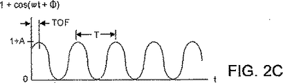
図2Aは、本発明において放射される典型的かつ理想的な周期的な光エネルギー信号、ここではcos(ωt)として表される信号の高周波成分を描写している。波形の周期Tは、T=2・π/ωで示される。信号は如何なる大きさのオフセットも存在していないという意味で、AC結合されているかのように描写されている。以下に記述するように、送信された信号の動作周波数は好ましくは数百MHzの範囲内であり、平均送信電力及びピーク送信電力は例えば約50mW以下など、比較的弱いものである。 FIG. 2A depicts the high frequency component of a typical and ideal periodic light energy signal emitted in the present invention, here represented as cos (ωt). The period T of the waveform is represented by T = 2 · π / ω. The signal is depicted as if it were AC coupled in the sense that there is no offset of any magnitude. As will be described below, the operating frequency of the transmitted signal is preferably in the range of several hundred MHz, and the average and peak transmission powers are relatively weak, for example, about 50 mW or less.
送信されたエネルギーの一部分はターゲットの対象物に到達し、少なくとも一部分は本発明の装置の方向へ反射され検出される。図2Bは、送信された波形の帰還してきたものを描写し、A・cos(ωt+φ)で表される。ここで、Aは減衰係数、φは本発明の装置からターゲットの対象物までの距離を横断するためにかかるエネルギーの飛行時間(TOF)の結果として生じる位相シフトがある。TOFを知ることは、例えばターゲット20のようなターゲット対象物上の点から、本発明によるシステム内の検出器のアレイ中の受信画素検出器までの距離zを知ることと等しい。
A portion of the transmitted energy reaches the target object and at least a portion is reflected and detected in the direction of the device of the present invention. FIG. 2B depicts the returned waveform of the transmitted waveform and is expressed as A · cos (ωt + φ). Where A is the attenuation coefficient and φ is the phase shift resulting from the time of flight (TOF) of energy taken to traverse the distance from the device of the invention to the target object. Knowing the TOF is equivalent to knowing the distance z from a point on the target object, such as the
図2Cは、本発明ではDCオフセットが存在していること除いて、図2Bに示したものと同様である。図2Bで示した波形は1+A・cos(ωt+φ)として表すことができる。後述するように、フォトダイオードをバイアスする幾つかの実施例ではDCオフセットが望ましいが、基礎となる数学的計算にそれほど影響を与えるものではない。繰り返すが、図2Cの波形の周期Tは、図2A及び図2Bに示してあるように、T=2・π/ωであるものとする。 FIG. 2C is similar to that shown in FIG. 2B, except that there is a DC offset in the present invention. The waveform shown in FIG. 2B can be expressed as 1 + A · cos (ωt + φ). As will be described below, DC offset is desirable in some embodiments for biasing the photodiode, but does not significantly affect the underlying mathematical calculations. Again, it is assumed that the period T of the waveform in FIG. 2C is T = 2 · π / ω, as shown in FIGS. 2A and 2B.
図2D及び図2Eは、ここで使用しているデューティーサイクルの概念を理解する際に有用である。図2Dで示すようなパルスタイプの周期的な信号では、デューティーサイクルdは、時間の比TH/Tで定義され、ここでTHは信号が所与の閾値VHより高い時間で、Tは信号の周期である。閾値レベルVHは通常、最大信号レベルと最小信号レベルの平均である。本発明の内容においては、THがフォトダイオード検出器240−Xがその間に変調される時間を表すことを除いて、上記の定義は類似しており、図2Eで示すようにTは発光器220の変調をオンにしたりオフにしたりする繰り返し期間である。本発明の内容においては、平均電力を一定に保つために光エネルギー発光器220のピーク電力放射を適切に調整すれば、TH/Tを減少させることができる。記述したとおり、発光器220によって放射される光エネルギーが周期的であれば、それらは方形波あるいは方形波のようなものである必要はない。図2Eで示したような波形を放射し検出することができる。しかしながら、デューティーサイクルの上記定義は、図2Eのような波形にも適用できるものとする。
2D and 2E are useful in understanding the concept of duty cycle used here. For a pulse-type periodic signal as shown in FIG. 2D, the duty cycle d is defined by a time ratio T H / T, where T H is the time when the signal is above a given threshold V H and T Is the period of the signal. The threshold level V H is usually the average of the maximum signal level and the minimum signal level. In the context of the present invention, the above definition is similar except that T H represents the time during which the photodiode detector 240-X is modulated, and T is the light emitter as shown in FIG. 2E. This is a repetition period in which the 220 modulation is turned on and off. In the context of the present invention, T H / T can be reduced if the peak power emission of the
送信された周期的な光エネルギー信号の繰り返し率を特定することは、送信された波形及びデューティーサイクル、距離zを解像する際の望ましい精度及び光エネルギー発光器のピーク電力必要条件の考察を含むトレードオフを伴う。例えば、検出された位相シフト情報を8ビットでアナログ−デジタル変換すると仮定すると、その高周波成分が、例えば200MHzといったように数百MHzである周期的な送信信号は、cm程度の距離zの解像度と一致している。実際には、連続的な正弦タイプ波形を仮定すると、光エネルギー発光器から要求されるピーク電力は約10mWである。もちろん、仮に送信波形のデューティーサイクルが1%に減少したとすると、光エネルギー発光器のピーク電力を約500mW程度に増加させなければならない。低ピーク電力の発光器を使用する能力が、本発明と先に参考文献とした出願人の米国特許6,323,942B1(2001年)との間の違いを示す要素の一つであると理解できる。 Identifying the repetition rate of the transmitted periodic light energy signal includes consideration of the transmitted waveform and duty cycle, the desired accuracy in resolving the distance z, and the peak power requirements of the light energy emitter. With trade-offs. For example, assuming that the detected phase shift information is converted from analog to digital by 8 bits, a periodic transmission signal whose high-frequency component is several hundred MHz, such as 200 MHz, has a resolution of a distance z of about cm. Match. In practice, assuming a continuous sinusoidal waveform, the peak power required from the light energy emitter is about 10 mW. Of course, if the duty cycle of the transmission waveform is reduced to 1%, the peak power of the optical energy light emitter must be increased to about 500 mW. It is understood that the ability to use low peak power light emitters is one of the factors that show the difference between the present invention and applicant's previously referenced US Pat. No. 6,323,942B1 (2001). it can.
次に、図3を参照として、本発明の位相シフト情報の処理と使用について記述する。図3は、1つのIC210上に製作されることが好ましい三次元イメージングシステムである本発明200を描写するブロックダイヤグラムである。システム200は、可動部分を必要とせず、チップ外の部品が比較的少なくてよい。図3は、参考文献とした出願人の同時系属の実用新案出願から抜粋したものであり、図3の様々な素子の回路の詳細は異なるものの、本発明を説明するために使用することが可能である。概要としては、本発明の様々な実施例において、アレイ230中の各光検出器240−xが、光検出器内でQE変調を実施する関連エレクトロニクス250−xを有することが好ましい。可変位相遅延あるいは固定位相遅延のどちらの技術を使用するにしても、本発明ではz=φ・C/2・ω=φ・C/{2・(2・π・f)}によって、距離zを決定する。
Next, processing and use of the phase shift information of the present invention will be described with reference to FIG. FIG. 3 is a block diagram depicting the
システム200は、例えば数百MHzの繰り返し率で駆動される場合、50mW程度のピーク電力を出力できる低ピーク電力レーザーダイオードや低ピーク電力LEDといった発光器を含んでおり、かつ好ましい実施例では、ここに定義されるようにデューティーサイクルが100%に近い。現在では、有用な発光器は、バンドギャップエネルギーがCMOS IC210の好ましい素材であるシリコンとは大きく異なる、AlGaAsのような素材から作られる。それゆえ、図3では発光器220は210のチップ外であるように描写してあるが、発光器220を囲んでいるファントムラインは、代わりにCMOSコンパチブル素材から作られる発光器220をIC210上に製作してもよいことを表している。
The
光源220は、他の波長でもかまわないができれば800nmの波長でエネルギーを放射する低ピーク電力LEDか、または、レーザーであることが好ましい。800nm以下の波長では、放射された可視光になり始め、レーザー作製はより難しくなる。900nm以上の波長では、CMOS/シリコンフォトダイオードの効率が急速に下がる。何れにせよ1100nmでは、IC210のようなシリコン基板上に製作された素子にとっては最も高い波長である。特定の波長を持った放射光を使用し、また異なる波長の入射光をフィルターにかけることによって、環境光の有無にかかわらずシステム200は作動する。システム200が暗闇内で機能できると、警備用及び軍用タイプのイメージング応用に有効である。チップ外に実装したレンズ290は、好ましくは画素検出器240xが視野内のある特定の一つの点(例えば対象物表面の点)からの光を受け取るように、フィルターした入射光をセンサーアレイ230上に集光する。
The
光波の伝達の特性により、普通のレンズ290を用いて光をセンサーアレイ上に集光することができる。レンズ(290´)が、発光器220から送信された光エネルギーを集光する必要がある場合、ミラータイプの配置を使用するとすると、290と290´には単一レンズが使用される。一般的なLEDまたはレーザーダイオード発光器220は、おそらく100pF程度の分流容量を有する。それゆえ発光器220を駆動する際、小さなインダクタンス(おそらく数nH程度)を容量と並列に配置し、結合したインダクタンス―容量が通常数百MHzという発光器の周期的な周波数で共振するようにすることが有利である。その代わりにインダクタンス(ここでも数nH)は、発光器とその寄生容量に直列結合することができる。そのようなインダクタンスは必要に応じて、発光器へのボンディングワイヤーを使用して作ることができる。
Due to the characteristics of light wave transmission,
CMOSコンチパブルIC210の上には、発振器225ドライバー、(おそらく100×100の(またはそれ以上の)画素検出器240と100×100(またはそれ以上の)関連エレクトロニクス処理回路250から成る)アレイ230、マイクロプロセッサーまたはマイクロコントローラーユニット260、(好ましくはランダムアクセスメモリーすなわちRAMと読み出し専用メモリーすなわちROMを含む)メモリー270、例えばアレイ230中の様々な画素検出器によって検出される位相情報φの8ビットのA/D変換を供与するアナログ/デジタル(A/D)変換ユニットを含む様々な計算及び入力/出力(I/O)回路構成280を製作することが好ましい。実施によっては、各エレクトロニック処理回路250の一部分として、単一のチップ上に(A/D)コンバーター機能を供するか、または専用のA/Dコンバーターを設置する。I/O回路280は、エネルギー発光器220を駆動する発振器225の周波数をコントロールする信号も与えることができることが好ましい。
On top of the CMOS
図3に示したDATA出力ラインは、アレイ230中の様々な画像検出器240からの位相シフト情報を用いて本発明によって計算する情報の一部分あるいは全てを表している。好ましくは、マイクロプロセッサー260が視野シーン内の対象物を識別するために、RAM270に蓄積された連続するフレームを調べる。それからマイクロプロセッサー260は距離zを計算し、対象物の速度dz/dt、dx/dt、dy/dtを計算することができる。更に、マイクロプロセッサー260と関連するチップ上の回路構成は、例えばシステム200を用いたアプリケーションがバーチャル入力デバイスを伴ったユーザーインターフェースを検出する場合には使用者の指といった具合に、所望されるイメージの形を認識するようにプログラムすることができる。そのようなアプリケーションでは、マイクロプロセッサー260によって与えられたデータは、キーストローク情報に変換される。この情報の一部分または全て(図3ではDATAとして示してある)は、更なる処理をするために例えばユニバーサルシリアスバスを経由して、このICから外部のコンピューターに転送することもできる。もしマイクロプロセッサー260が十分な計算能力を有していれば、追加的なチップ上の処理も行ってもよい。必要に応じて、CMOSコンチパブル検出器240のアレイからの出力にランダムな方法でアクセスし、それによりTOFデータを如何なる順序ででも出力できることも留意すべきである。
The DATA output lines shown in FIG. 3 represent some or all of the information calculated by the present invention using phase shift information from the
その他の機能としては、インターフェース回路280を通じて作動するマイクロプロセッサー260は、例えばf1=200MHzといった所望される周波数、所望されるデューティーサイクルでドライバー225を周期的に発振させる。発振器ドライバー225からの信号に応答して、レーザーダイオードまたはLED220は、例えばf1=200MHzといった所望される周波数、デューティーサイクルで光エネルギーを放射する。ここでも数学的説明を容易にするため正弦波形または余弦波形を想定しているが、例えば方形波のような、類似したデューティーサイクル、繰り返し率、ピーク電力である周期的な波形を使用してもよい。記述したように、本発明では例えば10mWといったように、平均電力及びピーク電力がかなり低いという効果がある。その結果、米国特許6,323,942B1(2001年)に記載されている出願人の先の発明における高ピーク電力レーザーダイオードでは何ドルもの費用がかかるのに対して、LED発光器220の費用は30セント程度である。
As another function, the
周期的な高周波成分が理想的にはS1=cos(ωt)で表現される光エネルギーは、ある距離z離れたところにあるターゲット対象物20上にレンズ290′によって集光される。ターゲット20に降りかかる光エネルギーの少なくとも一部分はシステム200に向かって反射され、アレイ230中の1つ以上の画素検出器240によって検出される。システム200、より詳しくはアレイ230中の任意の画素検出器240と対象物20上のターゲット点を隔てる距離zのために、位相は検出された光エネルギーが飛行時間つまり隔てる距離zに比例するある量φだけ遅延する。異なる画素検出器240によって検出される入射光エネルギーは、異なる飛行時間または距離zが関係するため、異なる位相φを持ち得る。図3を含む様々な図では、入射光エネルギーはS2=A・cos(ωt+φ)で表され、例えば実際にはDC成分を含む帰還信号のAC成分である。しかしながら、DC成分は、比較的重要性はなく、図示はしていない。
The light energy in which the periodic high-frequency component is ideally expressed by S 1 = cos (ωt) is collected by the
後述するように、マイクロプロセッサー260及びマイクロプロセッサーによって実行されるメモリー270に搭載したソフトウェアと提携して、相対位相遅延を調べ決定することは、アレイ230中の各画素検出器240に関連したエレクトロニクス250の機能である。バーチャルキーボードといったような、システム200がデータ入力メカニズムをイメージするアプリケーションでは、マイクロプロセッサー260が、幾つかのバーチャルキーのうちどれが、あるいは例えばバーチャルキーボードのようなバーチャルデバイスのどの領域が、使用者の指またはスタイラスで触られたかを識別するのに十分な検出データを処理する。それゆえシステム200からのDATA出力は様々な情報を含む。こうした情報は、距離z、対象物20の速度dz/dt(及び/またはdx/dt、dy/dt)の情報や、例えば使用者の手またはスタイラスによって触れられたバーチャルキーの識別のような対象物の識別を含むが、こうした例に限られるわけではない。
As described below, in conjunction with the
好ましいIC210はまた、マイクロプロセッサーまたはマイクロコントローラーユニット260、(好ましくは、ランダムアクセスメモリーすなわちRAMと読み出し専用メモリーすなわちROMを含む)メモリー270及び様々な計算、入力/出力(I/O)回路280を含む。例えば、I/O回路280からの出力は、エネルギー発光器220を駆動する発振器225の周波数をコントロールすることができる。他の機能としては、コントローラーユニット260は、対象物までの距離zと対象物の速度(dz/dt、dy/dt、dx/dt)の計算を行うことができる。図3で示したDATA出力ラインは、様々な画素検出器240からの位相シフト情報を用いて本発明によって計算されたそのような情報の一部分または全てを表している。
The
画素センシング検出器の二次元アレイ230は、標準的な商業用のシリコン技術を使用して製作することが好ましい。これにより、回路225、260、270、280だけでなく、様々な画素検出器240とそれらの関連回路250を含み、好ましくはエネルギー発光器220も含んだ単一IC210を製作できるという効果がある。当然のことながら、画素検出器のアレイと同一IC上にそのような回路とコンポーネントを製作できれば、信号パスが短くなり、処理時間及び遅延時間を短縮することが可能である。図3では、システム200は集光レンズ290及び/または290′を含んでいてもよいが、それらのレンズはICチップ210外にに製作されるものとする。
The two-
各画素検出器240は、電流源、理想的なダイオード、分流インピーダンス、ノイズ電流源の並列結合と等しく、その上に降りかかってくる入射フォトン光エネルギーの量に比例する電流を出力する。CMOS画素ダイオードまたはフォトゲート検出器素子のアレイを実現するために、CMOSファブリケーションを利用することが好ましい。典型的なフォトダイオード製造技術は、井戸への拡散、基板への拡散、井戸から基板へのジャンクション及びフォトゲート構造を含む。井戸から基板構造のフォトダイオードは、赤外線(IR)に対する感度がより高く、少ない容量を示し、それゆえ、基板への拡散構造のフォトダイオードよりも好まれる。
Each
記述したように、図4は出願人の同時係属実用新案出願に記載された実施例を表している。図4はIC210の一部分とアレイ230の一部分を示しており、240−1から240−xの画素検出器と、250′−1から250′−xの典型的なダイオード関連エレクトロニクスを描写する。図4を含む様々な図では、分かりやすく図示するため、レンズ290は図示していない。図4は本発明に直接的には関係していないが、本発明がもたらす利益を評価するために、またよりよく理解されるように含めてある。その後に続く説明では、図9A−9Cはカテゴリー1のVPDでのQE変調技術のためのもので、図10A―10Cはカテゴリー2の固定位相変調技術のためのものであり、残りの図はこれら様々な技術の特徴を図示している。
As described, FIG. 4 represents an embodiment described in Applicants' co-pending utility model application. FIG. 4 shows a portion of
実際のアレイは何百何千かそれ以上の画素検出器と関連エレクトロニクス回路を含んでいるが、図4は分かりやすく図示するために、2つの画素検出器240と2つの関連エレクトロニクス回路250′だけを図示している。記述したように、必要に応じてICチップ210上にオムニバスA/D機能の実施するのではなく、専用A/Dコンバーターを各エレクトロニクス回路250′―1から250′―xの一部として設置することができる。
Although the actual array includes hundreds or thousands of more pixel detectors and associated electronics circuits, FIG. 4 is shown with only two
次に、画素検出器240−1による入射光エネルギーの検出について考える。低電力LEDまたはレーザーダイオード等220が理想的な高周波成分S1=cos(ω・t)を有する光放射光を放射すると仮定すると、(距離がz離れたところにある)ターゲット20の表面上の点で反射されたそのような放射光の一部分は、S2=A・cos(ω・t+φ)で与えられる。この入射する放射光を受け取ると、画素検出器240−1は低ノイズ増幅器300が増幅する信号を出力する。典型的な増幅器300は、12dB程度の閉ループ利得を有する。
Next, detection of incident light energy by the pixel detector 240-1 will be considered. Assuming that a low power LED or laser diode or the like 220 emits light radiation having an ideal high frequency component S 1 = cos (ω · t), on the surface of the target 20 (distance away z) The portion of such emitted light reflected at the point is given by S 2 = A · cos (ω · t + φ). When this incident radiation is received, the pixel detector 240-1 outputs a signal amplified by the
記述したように、光源220からの周期的な放射は、数百MHzの高周波成分を持つ正弦または正弦のような形が好ましい。この高い光変調周波数にもかかわらず、関心のある周波数全てはこの変調周波数に近いため、増幅器300は100KHzまたはその程度のバンド幅、おそらく数十KHzという低いバンド幅があれば十分である。IC210上に何百何千という低ノイズの比較的低いバンド幅の増幅器300を設置することが、出願人の原発明におけるように狭いパルスを透過させる広バンド幅の増幅器を設置するより容易で、経済的な取り組みであることは、理解されるものである。それゆえ図4では、アレイ230は比較的小さなバンド幅の増幅器300で機能し、各増幅器の出力は関連ミキサー310の第一の入力に直接結合している。関連ミキサー310の2番目の入力は、第一の入力における周波数と同様の周波数を持つ信号である。各増幅器300と関連ミキサー310が単一のユニットとして実現されるならば、ユニット全体がおよそ数十KHzのバンド幅を持ち、高周波反応も数十KHz程度で足りる。
As described, the periodic radiation from the
図4に示したように、検出信号と送信信号を比較すると、TOFと距離zに関連した位相シフトφがある。各回路250′―xは、ミキサー310の第一の入力に関連する低ノイズ増幅器300の出力を結合する。図4で説明する出願人の先の発明では、ミキサー310はギルバートセルや乗算機などとして実現可能である。
本質的に各ミキサー310は、関連画素検出器240からの増幅された検出出力信号S2をジェネレーター225信号S1とホモダイン検波する。放出光エネルギーが正弦波か余弦波として表現される理想的な高周波成分を持つと仮定すると、ミキサー出力の積S1・S2は、0.5・A・{cos(2・ω・t+φ)+cos(φ)}であり、平均値は0.5・A・cos(φ)である。必要に応じて検出された帰還信号の振幅つまり輝度Aは、各画素検出器出力から別々に測定してもよい。実際には、A・cos(φ)の8ビットのアナログからデジタルへの解像度は、結果としてz測定における約1センチの解像度になる。
As shown in FIG. 4, when the detection signal and the transmission signal are compared, there is a phase shift φ related to the TOF and the distance z. Each
In essence, each
各ミキサー310は、可変位相遅延(VPD)ユニット320の出力に結合した第二の入力を有している。VPDユニット320は、様々な方法で実施することができる。例えば、各インバーターの信号を送るスピードを速めたり遅くしたりするように動作電力供給電圧が変化する、直列結合した一連のインバーターを使用するといった方法である。各VPDユニット320への第一の入力は信号ジェネレーター225で作られ、S1=cos(ωt)であり、精々信号係数を加えるか引くか与えるかしたものである。VPD320がジェネレーター225で作られたcos(ωt)信号に可変時間遅延ψを加えると想定する。そこでミキサー310は、増幅器300によって出力された増幅されたcos(ω・t+φ)信号と、VPD320によって出力されたcos(ω・t+ψ)信号を混合する。そして、ミキサー310は、0.5・A・{cos(φ−ψ)+cos(2・ω・t+φ+ψ)}を含む信号を出力する。ミキサー310の出力はローパスフィルター340の入力に結合する。フィルター340は好ましくは100Hz程度から数KHz程度のバンド幅を有する。かくして、フィルター340からの出力が、0.5・A・cos(φ−ψ)に比例する低周波信号になる。この低周波信号はここでインテグレーター330に入力される。インテグレーター330の出力は、画素検出器240―xに対するφxである。
Each
VDP320は、位相差が(φ−ψ)あるが発光器220が放射する変調周波数と同一の変調周波数をもった2つの信号によって駆動される。位相シフトがψ=φ±90度である場合、インテグレーター330の出力極性が変化することに留意すべきである。図4に示した構造では、各画素検知器240−xによって検出された帰還信号と関連した位相シフトψx=φx±90度が、画素検出器のインテグレーター330−xから得られる。
飛行時間による位相シフトφは、次のように求めることができる。
φ=2・ω・z/C=2・(2・π・f)・z/C
ここでCは、300,000Km/秒の光の速度である。したがって、エネルギー発光器220からアレイ230中の画素検出器240−xまでの距離zは、次のように求められる。
z=φ・C/2・ω=φ C/{2・(2・π・f)}
The
The phase shift φ according to the flight time can be obtained as follows.
φ = 2 · ω · z / C = 2 · (2 · π · f) · z / C
Here, C is the speed of light of 300,000 Km / sec. Accordingly, the distance z from the
z = φ · C / 2 · ω = φ C / {2 · (2 · π · f)}
距離zは、2πC/(2・ω)=C/(2・f)をモジュロとして分かる。f1、f2、f3・・・といった幾つかの異なる変調周波数を使用することによって、距離zはC/(2・f1)、C/(2・f2)、C/(2・f3)等をモジュロとして決定することが可能になり、更に、エイリアシングを避けるか、少なくとも減らすことができる。例えば、マイクロプロセッサー260はジェネレーター225に、例えばf1、f2、f3といった選択された周波数の正弦駆動信号を出力するよう命令することができる。例えばi=整数のようにf1、f2、f3が整数であるとすると、エイリアシングはLCM(f1、f2、f3)で表されるf1、f2、f3の最小公倍数にまで減少される。f1、f2、f3が整数でない場合には、a1/D、a2/D、a3/Dのように表現できる分数としてモデル化されるのが好ましい。ここでaiは、整数iで、D=GCD(a1、a2、a3)であり、ここでGCDは最大公約数を示す。そこで距離zは、LCM(a1、a2、a3)/Dをモジュロとして決定される。
The distance z is known as modulo 2πC / (2 · ω) = C / (2 · f). By using several different modulation frequencies such as f 1 , f 2 , f 3 ..., the distance z is C / (2 · f 1 ), C / (2 · f 2 ), C / (2 · f 3) makes it possible to determine the modulo the like, further, avoid or aliasing, it can be at least reduced. For example, the
各ミキサー310への2つの入力信号が、例えば回路実施に応じてψx=φx+90度またはψx=φx−90度のどちらか選択される位相において、お互いから90度位相が外れた時図4の閉ループ帰還回路構成は安定した点に達する。適切な90度の位相外定常状態では、各ローパスフィルター340からの出力信号は、理想的にはゼロである。例えば、ローパスフィルター340信号の出力信号が正であるとすると、関連インテグレーター330からの出力信号は、ローパスフィルターの出力がゼロ状態に戻るように駆動する位相シフトを更に加えることになる。
The two input signals to each
帰還システムが定常状態の時、アレイ230内の画素検出機エレクトロニクス250′−xは、ψX=φX±90度として、ψ1、ψ2、ψ3・・・ψNといった様々な位相角度を提供する。例えばエレクトロニクス280に関連するアナログ/デジタル変換機能を使用するなどして、アナログフォーマットからデジタルフォーマットへ位相角度を変換することが好ましい。必要に応じてエレクトロニクス250′−xは、全ての画素に対して一定の位相値を持つ信号を混合できる。マイクロプロセッサー260は、上記の数学的関係を使用して距離z(及び/または他の情報)を計算するためのソフトウェア、例えばメモリー270に搭載した、または搭載可能なソフトウェアを実行することができるという効果がある。必要に応じて、マクロプロセッサー260は、エイリアシングエラーを減少、あるいは削除したりすることによってシステムの性能を向上させるために、例えば、f1、f2、f3・・・といった不連続の周波数を出力するように、ジェネレーター225に命令することもできる。
When the feedback system is in a steady state, the pixel detector electronics 250 '-x in the
引き続き図4を参照すると、位相角度ψ=φ±90度を生み出すためには、様々な実施方法を用いることができる。所与のアプリケーションでは30フレーム/秒のフレーム率でイメージを得る必要があると仮定する。そのようなアプリケーションでは、約30msのサンプル率で、A/D変換がなされる間に位相角度ψをサンプリングすれば十分である。このサンプル率は、図4で示されるように、本来エレクトロニクス250′−x内に存在する比較的低いバンド幅と同等である。実際には、システム200は約1cmの距離zの解像度を供与することができ、実際のアプリケーションでは、zの範囲は100m程度もしくはそれ以下である。
With continued reference to FIG. 4, various implementations can be used to produce the phase angle ψ = φ ± 90 degrees. Assume that a given application needs to acquire an image at a frame rate of 30 frames / second. In such an application, it is sufficient to sample the phase angle ψ during A / D conversion with a sample rate of about 30 ms. This sample rate is equivalent to the relatively low bandwidth that is inherently present in electronics 250'-x, as shown in FIG. In practice, the
距離zは位相遅延ψから得られるTOF情報から決定されるが、ターゲット対象物20から戻る信号の相対輝度もまた、有用な情報を供与できることに留意する。帰還信号上の振幅係数「A」は相対輝度を示す。図4の帰還構造はローパスフィルター340からの最小出力信号を達成しようとするが、僅かな変更により最大ローパスフィルター出力信号を代わりに用いてもよく、そうすると出力信号は輝度係数Aを示すことになる。このような構造は、低ノイズ増幅器300の出力の別のコピーを変調するために、VPD320からの出力と共に90度位相のずれた信号を用いて実施することができる。こうして変調されたシグナルの平均振幅は、入射する検出された帰還信号における係数Aに比例する。
Note that the distance z is determined from the TOF information obtained from the phase delay ψ, but the relative luminance of the signal returning from the
出願人の先行発明の説明を完了したので、次に本発明の様々な実施例について、主に図9A―9C(カテゴリー1)と図10(カテゴリー2)を参照しながら記述する。本発明においては、(ここで図4で示しているような先行発明で使用されたような)専用のエレクトロニクスミキサーは使用せず、代わりに、量子効率(QE)変調技術を使用する。これらのQE変調技術は、検出された信号電荷を蓄積することができるという効果があり、検出光電流によって生成された高周波で小振幅の信号を直接測定しようとする方法よりも好まれる。 Having completed the applicant's description of the prior invention, various embodiments of the present invention will now be described with reference primarily to FIGS. 9A-9C (Category 1) and FIG. 10 (Category 2). In the present invention, a dedicated electronics mixer (as used in the prior invention as shown here in FIG. 4) is not used, but instead a quantum efficiency (QE) modulation technique is used. These QE modulation techniques have the effect of being able to accumulate detected signal charge and are preferred over methods that attempt to directly measure small amplitude signals at high frequencies generated by the detected photocurrent.
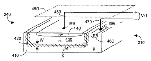
本発明によるQE変調回路トポグラフィーを分類する前に、MOSダイオードの働きと、MOSダイオード量子効率がいかにしてバイアスポテンシャル及び/またはフォトゲートポテンシャルによって変化するかということを記述することが有用である。図5A及び図5Bは、IC210の一部分を描写したもので、ここではpドープ基板410上に製作された様子を示した、単一フォトダイオード検出器240を描写したものである。フォトダイオード240には、幅がWであり、その上にはドーピング濃度の低いn領域430とドーピング濃度のより高いn領域440がある空乏層420が示してある。(ここでは、空乏層と空乏領域という言葉は同義として使用している。)n+ドープ領域440はフォトダイオード陽極として働き、それへの接続は450として示される。基板520の上部の領域に形成されたp+ドープ領域460はフォトダイオードの陰極として働き、それへの接続は470として示される。空乏幅がWである空乏領域480は、−領域430とp基板領域410の間に存在する。(ここで記述しているドーピング極性は反転してもよく、記述したp基板素材の上ではなくn基板素材の上に構造を製作することもできると理解されるものである。)
Before classifying the QE modulator circuit topography according to the present invention, it is useful to describe the behavior of the MOS diode and how the MOS diode quantum efficiency varies with bias potential and / or photogate potential. . FIGS. 5A and 5B depict a portion of
空乏領域480の幅Wは、フォトダイオード陽極450とフォトダイオード陰極470の間に加えられた逆バイアス電圧を変化すると、変化つまり変調する。このバイアスポテンシャルは図5AにおいてVr1と表され、図5BではVr2で表されている。図5A及び図5Bにおいては、Vr2>Vr1であり、結果として空乏領域の幅Wが増加する。
例えば、ターゲット20から反射されたエネルギーのような入射光エネルギーを表しているフォトンは、アレイ230中のフォトダイオード240―xの上に降りかかる。例えば図の中でも図3を参照のこと。フォトンは、これらのフォトダイオードの空乏領域と準中性領域に、電子―正孔ペアを生み出すことができる。これらの電子―正孔ペアは、再結合する前に比較的長い寿命をもつ。空乏領域に正孔のペアを生み出すフォトンは、基板の準中性領域に電子―正孔ペアを生み出すフォトンよりも、フォトン毎の光電流の発生がはるかに高いという効果がある。これは、空乏領域で生成される電子―正孔ペアは電界によって素早く掃引され、結果として生じる光電流に大きく寄与するからである。対照的に準中性領域で生成された電子―正孔ペアは暫くの間そこに留まり、光電流に実質的な寄与はないまま再結合をする可能性が高い。空乏層の幅Wを増加させることで、正孔ペアが生成され光電流に寄与するように素早く掃引されるような領域をより広く提供し、それによりフォトダイオードの量子効率が拡大する。
The width W of the
For example, photons representing incident light energy, such as energy reflected from the
関連分野の当業者には、空乏層の幅Wが以下のように表現されることがわかるだろう。
W=[2ε・(ψ0+VR−VB)]0.5{[qNA・(1+NA/ND)]}-0.5+[qND・(1+ND/NA)]-0.5}
ここで(VR−VB)は、フォトダイオード240の逆バイアス、NAとNdはそれぞれダイオードのn領域及びq領域へのドーピング濃度であり、ψ0=VTIn(NAND/ni 2)であり、ここでVT=kT/q=26mVで、n=1.5・1010cm-3である。
One skilled in the relevant arts will recognize that the width W of the depletion layer is expressed as:
W = [2ε · (φ 0 + V R −V B )] 0.5 {[qN A · (1 + N A / N D )]} −0.5 + [qN D · (1 + N D / N A )] −0.5 }
Here, (V R −V B ) is a reverse bias of the
本発明による量子効率(QE)変調では上記の等式から、フォトダイオード空乏幅Wをフォトダイオードの陽極、陰極の間に加えた様々な逆バイアスによって変調できることを認識する。これによりフォトダイオードの量子効率(QE)を変化させることを可能にし、結果としてシステム全体の検出の感度が向上する。表1は固定レベルの光にさらされた個別のPINフォトダイオードの典型的なデータを示しており、フォトダイオードに与えられた逆バイアス電圧の変化させた時のフォトダイオード電流の測定値である。CMOSで実施したフォトダイオードのデータは、もちろん表1のデータとは異なり得る。
In quantum efficiency (QE) modulation according to the present invention, it is recognized from the above equation that the photodiode depletion width W can be modulated by various reverse biases applied between the anode and cathode of the photodiode. This makes it possible to change the quantum efficiency (QE) of the photodiode, resulting in improved detection sensitivity of the entire system. Table 1 shows typical data for individual PIN photodiodes exposed to a fixed level of light and is a measurement of the photodiode current as the reverse bias voltage applied to the photodiode is varied. Photodiode data implemented in CMOS may of course differ from the data in Table 1.

表1で留意すべきことは、典型的なPINフォトダイオードでは、逆バイアスが0.5VDCから2VDCの間で変化するにつれて、フォトダイオード電流(例えば光電流)の大きさはが4倍に変化することである。
フォトダイオード逆バイアスの変調は、アレイ中のフォトダイオードの検出感度を向上させるためにQEを変化させるメカニズムである。しかしながら、更に効率的なQE変調検出の実施においては、フォトゲート構造を使用する。そのような実施例では、フォトゲートは、フォトダイオード構造のゲートに加えたポテンシャルを変えることによってQEを変調するフォトゲートMOSフォトダイオードとして実施されることが好ましい。
It should be noted in Table 1 that for a typical PIN photodiode, the magnitude of the photodiode current (eg photocurrent) changes by a factor of four as the reverse bias varies between 0.5 VDC and 2 VDC. That is.
Photodiode reverse bias modulation is a mechanism that changes the QE to improve the detection sensitivity of the photodiodes in the array. However, a more efficient QE modulation detection implementation uses a photogate structure. In such embodiments, the photogate is preferably implemented as a photogate MOS photodiode that modulates the QE by changing the potential applied to the gate of the photodiode structure.
次に図6A及び図6Bを参照して、基板410がpタイプ素材で、それぞれSとDするMOSタイプのソース領域とドレイン領域がnドープ素材のものであると仮定する。しかし先に記述したようにドーピング極性はもちろん逆でもかまわない。また、ソースSとドレインDは、図6Aで示したように互いに結合していると仮定する。ゲートGに与えた電圧S1(t)が高い時、ここでもnチャンネル素子であると仮定すると、素子240−xは空乏化し、それから反転する。この構成では、ゲートGとその下にある薄い酸化物(TOX)は、入射フォトンエネルギーS2(t)に対し実質的に透明であると仮定する。この条件は、ゲートGを作るために使われるポリシリコン素材がポリサイド化していない場合に満たされる。
6A and 6B, it is assumed that the
図6A及び図6Bを参照すると、ゲート構造GはS2(t)で示される入射光エネルギーに対し実質的に透明である。図6Aで示した構造は、S及びDで表されるソース領域及びドレイン領域の両方を含んでいる。対照的に図6Bの構造は、量子効率変調を向上させるために、ドレイン構造がないものである。図6Aではソース領域とドレイン領域が互いに結合しているので、素子240xは、図6Bで示したようにドレイン領域なしで作動することができる。記述したようにIC70を実現するためには、MOS製造プロセスを用いることが好ましい。それにより本発明が実施されている。多くのMOSファブリケーションプロセスでは、図6Bに示すように素子240xのドレイン領域は省かれてもよい。ドレイン領域を効果的に省略することによって、低感度動作状態と高感度動作状態の間の素子の収集効率の相対的変化を増加させる。以下に記述するように、光透明ゲートポテンシャルのバイアスの変化は、空乏層の形を変化させる。実質的にソース領域だけに限られた層480はゲートバイアスが低い時に存在し、その空乏層領域480′はゲートバイアスが高い時には、実質的にはゲート領域の下にまで及ぶ。
Referring to FIGS. 6A and 6B, the gate structure G is substantially transparent to the incident light energy denoted S2 (t). The structure shown in FIG. 6A includes both a source region and a drain region represented by S and D. In contrast, the structure of FIG. 6B has no drain structure to improve quantum efficiency modulation. In FIG. 6A, since the source region and the drain region are coupled to each other, the device 240x can operate without the drain region as shown in FIG. 6B. In order to realize the
例えばEH1、EH2などの光電荷は、フォトンエネルギーS2(t)に応答してゲート領域下の基板で生成される。ゲート領域にチャンネルが存在しない場合には、ほとんどの光電荷が失われ、ソース領域とドレイン領域だけが光電荷を集める。しかし、ゲートの下の領域が反転及び/または空乏化していると、生成された光電荷は捕らえられソース領域とドレイン領域に掃引される。これによりフォトン収集構造240−xの効率が効果的に増加する。収集効率の増加は、ゲートG下の面積とソース領域及びドレイン領域の面積つまりSとDの面積との比率に大体比例する。フォトゲートダイオード240xが適当な大きさの場合、この比率は10:1またはそれ以上である。この効率は突然増加し、電圧S1(t)が閾値を超えると効率が急に増加する。チャンネル部分がドープされておらず基板ドーピング1017以上の場合、閾値は約0Vであり、フォトゲート光検出器240xは約−0.1Vのゲート電圧で低感度モードであり、ゲート電圧が約+0.1の時には高感度モードになる。ゲート電圧の比較的小さな変化が、素子の感度に大幅な変化をもたらすことが分かるだろう。 For example, photocharges such as EH1 and EH2 are generated in the substrate under the gate region in response to photon energy S2 (t). In the absence of a channel in the gate region, most of the photocharge is lost and only the source and drain regions collect the photocharge. However, if the region under the gate is inverted and / or depleted, the generated photocharge is captured and swept into the source and drain regions. This effectively increases the efficiency of the photon collection structure 240-x. The increase in collection efficiency is roughly proportional to the ratio between the area under the gate G and the areas of the source and drain regions, that is, the areas of S and D. If the photogate diode 240x is of an appropriate size, this ratio is 10: 1 or higher. This efficiency suddenly increases, and when the voltage S1 (t) exceeds the threshold, the efficiency increases rapidly. When the channel portion is not doped and the substrate doping is 10 17 or more, the threshold is about 0V, the photogate photodetector 240x is in the low sensitivity mode with a gate voltage of about −0.1V, and the gate voltage is about +0. When set to 1, it is in high sensitivity mode. It can be seen that relatively small changes in the gate voltage result in significant changes in device sensitivity.
図6Cは、フォトゲートフォトダイオード240Xと、キャパシターC0に結合したより従来的なMOSフォトダイオードD1の間の回路がおよそ等しいことを示している。当然のことながら、MOSフォトダイオードの電圧レベルは、フォトゲートフォトダイオードの電圧レベルと異なる場合もある。したがって、フォトダイオード、光検出器、画素検出器240xという用語は、図6A−6Cに関連して上述したようなフォトゲートフォトダイオードを含むと理解される。同様に、ここで説明する従来的なMOSフォトゲートに関してのQE変調の様々な回路や分析も、上述したようなフォトゲートフォトダイオード240xに使用できると理解できる。分かり易く図示するため、ここでの実施例の殆どはフォトゲート検出器ではなくMOSタイプのフォトダイオード検出器に関して図示したが、どちらのタイプの検出器でも使用できる。 Figure 6C shows the photogate photodiode 240X, that is approximately equal circuit between the capacitor C 0 conventional MOS photodiode than bound to D1. Of course, the voltage level of the MOS photodiode may be different from the voltage level of the photogate photodiode. Accordingly, the terms photodiode, photodetector, pixel detector 240x are understood to include a photogate photodiode as described above in connection with FIGS. 6A-6C. Similarly, it can be appreciated that various circuits and analyzes of QE modulation for the conventional MOS photogate described herein can be used for the photogate photodiode 240x as described above. For ease of illustration, most of the embodiments herein are illustrated with respect to a MOS type photodiode detector rather than a photogate detector, but either type of detector can be used.
図7A及び図7Bは、D1で示されるフォトダイオード検出器240の等価回路を描写し、寄生分流キャパシターC1を含む。図7Aは、変調信号がキャパシターC0を通じて結合している高側のQE変調の図示として参照してもよい。図7Bでは、変調信号はキャパシターC1を経由して結合され、図は低側のQE変調を図示している。図7Bでは、キャパシターC0は通常、画素検出器D1に関連したエレクトロニクス内の増幅器(図示はされていない)内に設置されている。
7A and 7B depict an equivalent circuit of the
図7Aの右部分では、V2に比例しているL1からの光電子放出を引き起こすように、励振源V2が、例えばレーザーダイオードやLEDのような発光器L1に結合されている。図7Aの左部分では、フォトダイオードD1がL1からそのようなフォトンエネルギーを受け取り、光電流I1がそれに応じて誘起される。フォトダイオードD1(例えば、アレイ230中のフォトダイオード240−x)は逆バイアスされるので、バイアス源V1が電圧オフセットを含むと理解できる。もう一つの方法として、入射信号を検出する前に、フォトダイオードのノードNdを初期化の間にプリチャージすることができる。図7A及び図7Bにおいて、V2は周期的な波形のジェネレーター225に類似しており、L1は光エネルギー発光器220に類似していることが分かる。(他の図中の図を参照)
In the right part of FIG. 7A, an excitation source V2 is coupled to a light emitter L1, such as a laser diode or LED, to cause photoelectron emission from L1 that is proportional to V2. In the left part of FIG. 7A, photodiode D1 receives such photon energy from L1, and photocurrent I1 is induced accordingly. Since photodiode D1 (eg, photodiode 240-x in array 230) is reverse biased, it can be seen that bias source V1 includes a voltage offset. Alternatively, prior to detecting the incident signal, it is possible to precharge the node N d of photodiode during initialization. 7A and 7B, it can be seen that V2 is similar to the
図7A及び図7Bでは、フォトダイオードのバイアス電圧、したがってフォトダイオードのQEが、バイアス源V1によって変調される。図7Aでは、逆バイアス電圧がVd1=V1・(C0)/(C0+C1)によって与えられ、ここでC0はV1とD1の間に直列結合されている。表1と図5A及び図5Bから、大きな振幅のV1は、フォトダイオード空乏層領域の幅Wを有利に増加できる大きな逆バイアスを表す。これが今度はフォトダイオードD1(または240)の感度を増加し、その結果フォトダイオード電流I1が、L1から入射するフォトンエネルギー(または、ターゲット対象物20から反射され、入射するフォトンエネルギー)に対応して増加する。
7A and 7B, the bias voltage of the photodiode, and thus the QE of the photodiode, is modulated by the bias source V1. In FIG. 7A, the reverse bias voltage is given by Vd1 = V1 · (C 0 ) / (C 0 + C 1 ), where C 0 is coupled in series between V1 and D1. From Table 1 and FIGS. 5A and 5B, a large amplitude V1 represents a large reverse bias that can advantageously increase the width W of the photodiode depletion layer region. This in turn increases the sensitivity of the photodiode D1 (or 240) so that the photodiode current I1 corresponds to the photon energy incident from L1 (or the photon energy reflected from the
励振源V2及びバイアス源V1が同一の周波数(ω)で動作する場合、サイクル毎の電流ソースI1が与える総電荷はV1及びV2が同位相にある時、例えばV1(ωt)及びV2(ωt)の振幅が同時に高い時に最大となる。これは、入射フォトンエネルギーが最大強度である時つまり最も輝度が高い時に、フォトダイオードの感度が最大になることによる結果である。反対に、入射フォトンエネルギーが最大の時にD1感度が最小になるならば、I1によって供給されるサイクル毎の電荷の量は最小になる。 When the excitation source V 2 and the bias source V 1 operate at the same frequency (ω), the total charge provided by the current source I 1 for each cycle is, for example, V 1 (ωt) when V 1 and V 2 are in phase. ) And V 2 (ωt) are maximized at the same time. This is a result of the maximum sensitivity of the photodiode when the incident photon energy is at its maximum intensity, that is, when the luminance is highest. Conversely, if the D1 sensitivity is minimized when the incident photon energy is maximized, the amount of charge per cycle delivered by I 1 is minimized.
所与のサイクル数後のフォトダイオードノードNd上の電荷ΔQNの量の変化は、そのサイクルの間にI1によって供給された電荷の量である。キャパシターC0及びC1が光電流I1によって放電される前後におけるノードNd上の電圧ΔVDの差を測定することによってΔQNの変化は決定される。通常、光電流I1は非常に小さく、直接測定することが困難である。しかしながら、多くのサイクル後の蓄積効果の結果、測定可能な電圧の変化ΔVDになる。 The change in the amount of charge ΔQ N on the photodiode node N d after a given number of cycles is the amount of charge delivered by I 1 during that cycle. The change in ΔQ N is determined by measuring the difference in voltage ΔV D on node N d before and after capacitors C 0 and C 1 are discharged by photocurrent I1. Usually, the photocurrent I 1 is very small and difficult to measure directly. However, the accumulation effect after many cycles results in a measurable voltage change ΔV D.
フォトダイオードの陽極端子及び陰極端子それぞれが図5Bの任意の電圧にセットされる場合、C0の上部リードを図7Bに示されるようにグランドポテンシャルにあるようにできる。いくつかの実施例に関して後述するように、一般的にノードNdは増幅器入力に結合していて、分流キャパシターも同一入力ノードに結合している。図7Bの構成の効果は、増幅器の寄生分流容量を、追加のキャパシターまたは専用の分流キャパシターの代わりにC1として使用できることである。そのようにすることで、部品の数を減らし、ICチップ上で本発明を実施するために必要とする面積を減らすことができる。更に、この構成ではノイズが少なく、生産技術における変動に過敏でない。 If the anode and cathode terminals of the photodiode are each set to the arbitrary voltage of FIG. 5B, the upper lead of C 0 can be at ground potential as shown in FIG. 7B. As will be described below with respect to some embodiments, node Nd is typically coupled to the amplifier input and a shunt capacitor is also coupled to the same input node. The effect of the configuration of FIG. 7B is that the parasitic shunt capacitance of the amplifier can be used as C 1 instead of an additional capacitor or a dedicated shunt capacitor. By doing so, the number of parts can be reduced and the area required to implement the present invention on an IC chip can be reduced. In addition, this configuration has low noise and is not sensitive to variations in production technology.
フォトンエネルギーがフォトダイオードに降りかかる際、入射フォトンエネルギーの到着と、放出された電子の収集には時間的遅れがある。この時間的遅れは、光エネルギーの波長が長く成るにつれ大きく増加し、約850nmの波形の場合数ns程度である。したがって、光エネルギー発光器225は、アレイ230中のフォトダイオード240−xが早い反応をし、高い周波数ωでQE変調できるように、短い波長を放射するように選択される。
When photon energy falls on the photodiode, there is a time delay between the arrival of incident photon energy and the collection of emitted electrons. This time delay increases greatly as the wavelength of light energy becomes longer, and is about several ns for a waveform of about 850 nm. Thus, the
当然のことながら本発明の様々な実施例で使用されるフォトダイオードは、効果的に検出するだけでなく、素早く検出することが望ましい。比較的短い波長の光エネルギーを送信できる発光器220を利用すれば検出器の効率性を促進するが、そのような発光器を製作することは長波長のエネルギーを与える発光器よりも高価になる。例えば、比較的安価なレーザーダイオードを波長が850nm程度のエネルギーを送信するための発光器220として利用できる。そのような発光器は比較的安価ではあるが、長波長は画素検出器の構造内に例えば7μmといったように深く入り込み、その結果量子効率が損失し反応が遅くなる。
Of course, it is desirable that the photodiodes used in the various embodiments of the present invention not only be effectively detected, but also quickly detected. Utilizing a
次に図7の典型的なCMOS構造を参照すると、ターゲット対象物20が反射した入射するフォトンエネルギーの大半が、画素検出器240のエピタキシャル領域410の奥深くで電子−正孔ペア(EHx)を作り出し、構造の更に奥深くにある領域412にも電子−正孔ペア(EHx’)を作り出すため、量子効率が落ちる。残念ながらこれらの深く放出された電子の多くは、光検出器の表面領域に到達できず、電子は表面領域で収集されるので、これらの電子はフォトダイオード検出信号電流には寄与することができない。更に、長めの波長を用いることで、信号電流が発生する前に好ましくない時間遅延が生じる。通常数nsのこの遅延は、フォトダイオード電流に寄与できるように深く放出された電子を収集する際に、拡散効果がドリフト効果より優位になるために起こる。
Referring now to the exemplary CMOS structure of FIG. 7, most of the incident photon energy reflected by the
仮にEHxとEHx’に関連する電子がどうにかしてフォトダイオード構造の表面領域近くに動かされたとすると、ドリフト効果が拡散効果より優位になり、より早く検出電流を見ることができる。エピタキシャル層410のドーピングが非常に低いため、エピタキシャル層の奥深くで作られた電子を比較的小さな電流を用いて動かすことが可能である。
If the electrons associated with EHx and EHx 'are somehow moved closer to the surface area of the photodiode structure, the drift effect is superior to the diffusion effect, and the detected current can be seen earlier. Since the doping of the
図7Cを参照すると、エピタキシャル層410は通常およそ7μmの厚さで、そのドーパント濃度は約NA=1015/cm3であり、その下にあるドーパント濃度の高い基板領域412はおよそ数百μmの厚さであり、そのドーパント濃度は約NA=1018/cm3である。図7Cに示すような構造は数多くの業者から簡単に入手可能である。
Referring to FIG. 7C, the
図7Cでは、n井戸領域430とP++領域460がエピタキシャル層410内に作られている。N+領域440はn井戸領域430と共に形成される。以下に記述するとおり、収集リード445と収集リード447を設けて深く放出された電荷を動かし、好ましくは上方へ動かしn井戸430により収集する。(記載したドーパント極性は、例えば代わりにn型の基板を使うなど逆にすることもでき、またドーパントレベルと構造の厚さは変更できるものとする。)
In FIG. 7C, an n-
次に、EHxに関連する電荷を上方に動かして一度電荷がn井戸に近づけば、最終的にはn井戸430が拡散効果により電荷を収集できるようにする方法について述べる。深く放出された電子を十分にゆっくりと促して、P++領域に関連するリード447ではなく、n井戸に関連するリード445に収集させることがゴールである。これから記述する方法では電子−正孔ペアEHxに関連する電子をうまく収集することはできるが、構造の更に奥深くに到達してEHx’に関連する電子をも収集することはできない。そのような動きを図7CのL型鎖線によって示す。EHx’の電子をも回収するには、層412に関連する高ドーパントレベルのために、許容できないような大きさの電流を必要とする。
Next, a method will be described in which the charge related to EHx is moved upward so that once the charge approaches the n-well, the n-well 430 can finally collect the charge by the diffusion effect. The goal is to encourage deeply emitted electrons sufficiently slowly to be collected by
次に本発明にしたがって電子を動かすために必要な電流の大きさについて考える。上から見て、図7Cに示す構造が1μmX1μmという大きさの正方形であり、その面積はAsで示されると想定する。領域410の厚さを7μmとすると、結果として体積は7X10-12/cm3となる。そのような体積から除去されなければならない必要電荷は、1015X10-8X7X10-4X1.6X10-19As=1.12X10-15Asであり、ここで1.6X10-19は電子一つに関連する電荷である。これだけの電荷を例えば1ns以内に除去することがゴールであるとすれば、必要な電流は約1.12μAとなる。この電流はごく僅かというわけではないが、光検出器アレイ230に関連する1平方マイクロンメートルごとにこの電流を提供することは実際に実行可能である。200MHzで変調されている1mmX1mmという大きさのアレイで、電子を7μm上方に動かすには電流は全体で約200mAとなる。基板領域412に関連するドーパントレベルが高いので、この方法を用いてEHx’から電子を回収しようとすることはできないことが理解できる。
Now consider the magnitude of the current required to move the electrons in accordance with the present invention. When viewed from above, the structure shown in FIG. 7C is a square size of 1μmX1μm is, assume that the area is represented by A s. If the thickness of the
したがって、深く放出された電子をどうにか層410から収集のために上方に動かすアプローチの一つは、実質的に全ての正孔を約7μm下方に掃引することである。電子と正孔の移動度はかなり近いので、こうして自由になった電子を少なくとも7マイクロン上方に動かすことができ、n井戸領域430に十分に近いところまでたどり着き、そこにある空乏領域の影響を好ましく受けさせることができる。空乏領域の影響は、そのような深く放出された電子が構造の上の方で収集されることを促進する。
Thus, one approach to somehow move deeply emitted electrons upward from the
n井戸領域430の下に好ましくはパルス電流を流すことにより、その高い移動度により電子を同じ距離だけ上方に動かしながら、正孔を下方に7μmほど動かすことができる。記述したとおり、一度電子が空乏領域がn井戸領域内に作り出す電界の影響を受けるのに十分な程近くに来ると、電子が収集される可能性は相当に高まる。
By passing a pulse current preferably under the n-
一実施例において、n井戸領域430の外の基板上にオーミックコンタクト460を形成し、電子を空乏層近くに持ってくることを促進するために使用する。このアプローチは、エピタキシャル層410のドーパント濃度が比較的低く、電子を上方に約7μm掃引するために要する電荷の大きさが許容可能なものであり、うまく働く。構造210の上部にあるドーパント濃度の高い領域においては正孔が多過ぎるため、電子を上方に7μm以上動かすことを推奨する理由はない。必要に応じて、オーミックコンタクトではなくキャパシター構造を用いたAC結合アプローチを代わりに用いてもよい。
In one embodiment,
次に、様々なタイプのエピタキシャル領域におけるドーピング勾配を用いた検出器構造について述べる。図7Dに示した構造は図7Cの構造に似ているが、図7Dの構造240’の深さは約7μmより深くてもよい。図7Dでは、エピタキシャル層410’が、比較的高い濃度(p1)から低めの濃度(p3)の範囲にわたる異なるドーパント濃度を規定することが好ましい。ドーパント濃度の推移は連続していてもよいし、例えば、それぞれ関連するドーパント濃度の別個のエピタキシャル層を形成するなど、段階的に成っていてもよい。 Next, detector structures using doping gradients in various types of epitaxial regions will be described. Although the structure shown in FIG. 7D is similar to the structure of FIG. 7C, the depth of the structure 240 'of FIG. 7D may be greater than about 7 μm. In FIG. 7D, the epitaxial layer 410 'preferably defines different dopant concentrations ranging from a relatively high concentration (p1) to a lower concentration (p3). The transition of the dopant concentration may be continuous, or may be stepwise, for example, forming separate epitaxial layers with each associated dopant concentration.
当業者ならば各ドーピング領域の境界線に関連する電界が存在することを知っている。構造の上表面に近づくにつれドーパント濃度が低くなる構造240’では、電界の方向は下向きに規定することができる。EHx’の中で領域412の上表面に近いところにある電子は、領域412とp1の間に存在するインターフェースを、そのインターフェースの電界によって、通り抜けて上方に動く。これらの電子は、そのインターフェースを通り抜けて下方には動かないため、次のエピタキシャルドーピングインターフェース(p1、p2)の近くに素早く上方に動くよう誘導できる(拡散効果により)可能性が非常に高く、それらの電子はそこから再び次のドーパント領域、ここではp2、に進入していくようにp1、p2に存在する電界によって誘導される。一度その(ドーパント濃度のより低い)エピタキシャル領域(ここではp2)に入ると、電子はまたp1、p2インターフェースを通り抜けて下方には動かなくなり、上方に動き次のドーパント領域(p3)の影響を受ける可能性が非常に高くなり、そこから更にその領域に進入すべく誘導される。
The person skilled in the art knows that there is an electric field associated with the boundary of each doping region. In structure 240 ', where the dopant concentration decreases as it approaches the upper surface of the structure, the direction of the electric field can be defined downward. Electrons in the EHx 'near the upper surface of the
当然のことながら、上述したのと同じ現象は、最初はエピタキシャル領域のどこかに開放されたEHxペアからの電子にも最初は働く。またエピタキシャル領域内に、二つ以下または四つ以上のドーパント濃度を規定することができることは理解される。 Of course, the same phenomenon as described above initially works for electrons from EHx pairs that are initially open somewhere in the epitaxial region. It will also be appreciated that less than two or more than four dopant concentrations can be defined within the epitaxial region.
したがって、エピタキシャル層から成るp1、p2、p3といった様々なインターフェースまたは境界線領域の中の電界に関連するドリフト電流現象は、p1、p2...のインタフェース領域の各々を通り抜けて電子が素早く上方に動くように誘導する。 Therefore, the drift current phenomenon associated with the electric field in various interfaces or boundary regions such as p1, p2, p3 made of epitaxial layers is p1, p2,. . . Through each of the interface areas to guide the electrons to move up quickly.
以上に記載したとおり、段階的にドープされたエピタキシャル領域は、その領域に進入するために十分な程近くに辿り着いた電子のための「ステージング」領域あるいは「ホールディング」領域として機能する。しかしながら、エピタキシャル領域410’全体を通じて連続したドーパント勾配が規定されるとすると、(別個のエピタキシャル領域は本来存在しないので)一つの領域内で「ホールディング時間」はない。その効果は、n井戸430による収集のために自由になった電子をより素早く捕らえて上方に掃引することである。 As described above, the step-doped epitaxial region functions as a “staging” region or “holding” region for electrons that have arrived close enough to enter the region. However, if a continuous dopant gradient is defined throughout the epitaxial region 410 ', there is no "holding time" within a region (since there is no separate epitaxial region). The effect is to capture the electrons freed for collection by the n-well 430 more quickly and sweep them upward.
以下のセクションでは差動QE変調と、それがもたらすことのできる効果について記述する。繰り返すが、差動QE変調を含むQE変調は、従来のMOSタイプのフォトダイオード検出器及び/またはフォトゲート検出器を用いて実施してもよい。 The following sections describe differential QE modulation and the effects it can produce. Again, QE modulation including differential QE modulation may be performed using a conventional MOS type photodiode detector and / or photogate detector.
再び図5A及び5Bを参照して、入射するフォトンエネルギーが、図示したフォトダイオードの基板内に、任意の位置「X」に発生させる電子−正孔ペアEH1を含む電子−正孔ペアを発生させるとする。図5Aでは、位置Xは準中性領域であり、空乏領域(斜線で示した部分)ではない。本発明において、この時点で変調がQEを減らし、EH1を含む可能な限りの数の電子−正孔ペアを放棄することが望ましい。例えばフォトダイオードの逆バイアスを増加させるなどして、フォトダイオードのQEをそれからすぐに増加させたならば、位置Xを網羅するように空乏領域の幅Wを広げることができる(図5B参照)。 Referring again to FIGS. 5A and 5B, the incident photon energy generates an electron-hole pair including an electron-hole pair EH 1 to be generated at an arbitrary position “X” in the illustrated substrate of the photodiode. Suppose that In FIG. 5A, the position X is a quasi-neutral region and not a depletion region (a portion indicated by hatching). In the present invention, it is desirable at this point that the modulation reduces QE and abandon as many electron-hole pairs as possible, including EH 1 . If the photodiode QE is immediately increased, for example, by increasing the reverse bias of the photodiode, the width W of the depletion region can be increased to cover the position X (see FIG. 5B).
図5Bにおいて、EH1はこの時点では空乏領域にある位置Xにまだ残存しており、EH1は今度は光電流に大きく寄与する。一方では図5Bにある増加した空乏領域が、フォトン検出感度を高めることができる。しかし、QEが低い時(図5A)にフォトンが入ってきた時に発生した電子−正孔ペアは、QEが高い時(図5B)に全光電流に寄与することができる。例えば、その寄与は別の時点でなされことになる。好ましくない結果としては、高変調率で効果的にQEを変更できないことである。しかしながら、高QE時に入ってきたフォトンのみが常に光電流に寄与することが好ましい。 In FIG. 5B, EH 1 still remains at position X in the depletion region at this point, and EH 1 now contributes greatly to the photocurrent. On the other hand, the increased depletion region in FIG. 5B can increase photon detection sensitivity. However, electron-hole pairs generated when photons enter when QE is low (FIG. 5A) can contribute to the total photocurrent when QE is high (FIG. 5B). For example, the contribution will be made at another time. An undesirable result is that the QE cannot be changed effectively at high modulation rates. However, it is preferable that only photons that enter during high QE always contribute to the photocurrent.
上述した時間的遅れ効果を取り除くことによって、より早いフォトダイオードQE変調を達成することが望ましい。環境光と所謂フォトダイオード暗電流とによって生じるフォトダイオード出力信号共通モード効果を除去することが、更に望ましい。全体として、QE変調は基本的にフォトダイオード構造内で電子のための収集ターゲットの大きさを変調することであるとわかる。他に収集ターゲットがなければ、たとえ小さなターゲットであって、ほとんどの電子は比較的長い寿命のために最終的には収集されることになる。したがって、電子の数に関しては、QE変調はターゲットエリアの変化に比べて相当に少ない。 It is desirable to achieve faster photodiode QE modulation by removing the time delay effect described above. It is further desirable to eliminate the photodiode output signal common mode effect caused by ambient light and so-called photodiode dark current. Overall, it can be seen that QE modulation is basically modulating the size of the collection target for electrons within the photodiode structure. Without other collection targets, even small targets, most electrons will eventually be collected for a relatively long lifetime. Therefore, with respect to the number of electrons, QE modulation is considerably less than changes in the target area.
代替隣接ターゲットの大きさを拡大したり縮小したりしながら、収集ターゲットの大きさを拡大したり縮小したりする差動QE変調技術を使用する本発明の様々な要素について次に記述する。その効果は、与えられたフォトダイオードのターゲットエリアを縮小しながら、電子と正孔のための大きな代替ターゲットを提供することである。これにより電子は寿命が尽きるよりかなり前に、代替ターゲットに収集され、縮小されたターゲットの対する循環から外されると共に、QEが高められる。 The various elements of the present invention that use differential QE modulation techniques that increase or decrease the size of the acquisition target while increasing or decreasing the size of the alternative adjacent target are now described. The effect is to provide a large alternative target for electrons and holes while reducing the target area of a given photodiode. This allows electrons to be collected on the alternate target long before their lifetime expires, removing them from circulation for the reduced target and increasing QE.
本発明では、QE変調の最中にフォトダイオード内の幾つかの領域、通常は接合のドーパント濃度が低めの領域が、準中性領域になったり空乏領域になったり状態が入れ替わると認識している。これらの領域を最低限に抑えることができれば、フォトダイオードをより明確にQE変調することができる。本文で後に図8A及び図8Bに関して述べるように、そのような高められたQE変調は差動変調アプローチを用いて促進される。図8A及び図8Bは、AとBで示される180度離れた二つの隣接するフォトダイオードの「スナップショット」を表している。好ましくはアレイ230において、隣接するフォトダイオードAとフォトダイオードBはお互いに十分に近く表面積が小さく、それぞれが常に実質的に同じ量の入射するフォトンエネルギーを受ける。フォトダイオードグループAまたはバンクAとフォトダイオードグループBまたはバンクBを、それぞれのQEが180度位相外れになるように、すなわちフォトダイオードBのQEが最小の時にフォトダイオードAのQEが最大に達し、かつ逆もまた同様になるように、バイアス変調する。
The present invention recognizes that during QE modulation, some regions within the photodiode, typically regions with lower dopant concentration, become quasi-neutral or depleted. Yes. If these regions can be minimized, the photodiode can be QE-modulated more clearly. As described later with respect to FIGS. 8A and 8B, such enhanced QE modulation is facilitated using a differential modulation approach. 8A and 8B represent “snapshots” of two adjacent photodiodes separated by 180 degrees, designated A and B. FIG. Preferably, in
図8A及び図8Bで留意すべきことは、隣接するフォトダイオードAとBの間の準中性領域500は常にかなり小さいので、そこで作り出される電子−正孔ペアの数もかなり少ない。QE変調を減らすのは空乏領域付近の準中性領域なので、このことは好都合である。図8Bでは、フォトダイオードBのQEが増加した時、フォトダイオードAとフォトダイオードBのダイオードの間の準中性領域500にある電子−正孔ペアを隣接するフォトダイオードBのための光電流の中へ掃引してもよい。準中性領域500は小さいので、領域500によるQE変調の劣化が少なくて、有利である。
It should be noted in FIGS. 8A and 8B that since the
図8A及び図8Bにおいて、ある時にフォトダイオードAとフォトダイオードBはそれぞれ0VDCと2VDCで逆バイアスされると想定する。例えば、仮にAとBが適当なCMOS0.25μmプロセスにより製作されたとして、フォトダイオードBは通常フォトダイオードAに比べて最大で30%多くのフォトンエネルギーを変換する。フォトダイオードAのQEは0VDCから逆バイアスの僅かな増加に対して急速に増加するのに対し、1VDCほどで逆バイアスされたフォトダイオードBは、逆バイアスの僅かな変化ではほとんど影響を受けない。したがって、フォトダイオードAの逆バイアスが可能な限り小さいことが、最大QE変調にとっては有利である。このバイアス方式は、フォトダイオードAとフォトダイオードBの間の準中性領域500にチャンネルが形成されるMOSトランジスターに対応する。MOSトランジスターゲート構造は存在しないが、高いソース−ドレーン電圧下の閾値下の領域においてのある電圧値に対して存在すると想定できる。
8A and 8B, assume that photodiode A and photodiode B are reverse-biased at 0 VDC and 2 VDC, respectively. For example, assuming that A and B are manufactured by an appropriate CMOS 0.25 μm process, the photodiode B converts up to 30% more photon energy than the normal photodiode A. The QE of photodiode A increases rapidly from 0 VDC to a slight increase in reverse bias, while photodiode B reverse-biased at about 1 VDC is hardly affected by small changes in reverse bias. Therefore, it is advantageous for maximum QE modulation that the reverse bias of photodiode A is as small as possible. This bias method corresponds to a MOS transistor in which a channel is formed in the
図8Aに示したタイムフレームの間、フォトダイオードAには弱く逆バイアスをかける。結果として、フォトダイオードAとフォトダイオードBの間には相当量のの漏れ電流があり得、それは図8A及び図8Bに示すフォトダイオードAがソースとなりフォトダイオードBがドレーンとなっているMOSトランジスターの閾値下漏洩と合致する。そのような漏れ電流は、少なくともフォトダイオードAとフォトダイオードBの間の領域においては対象の光エネルギーに対して透明であると想定されるポリシリコンゲートG’を形成し、ゲートG’の下に薄い酸化物(TOX)の絶縁層を形成することによって減らすことができる。そのようなゲートを製作した場合、ゲート電圧をコントロールすることによって閾値下漏れ電流をコントロールできる。ドープされていないチャンネルについては、漏れ電流を大幅に減らすには通常約−0.4VDCのゲート電圧で十分である。 During the time frame shown in FIG. 8A, photodiode A is weakly reverse biased. As a result, there can be a significant amount of leakage current between photodiode A and photodiode B, which is the result of the MOS transistor having photodiode A as the source and photodiode B as the drain shown in FIGS. 8A and 8B. Matches subthreshold leakage. Such leakage current forms a polysilicon gate G ′ that is assumed to be transparent to the light energy of interest, at least in the region between photodiode A and photodiode B, and below gate G ′. This can be reduced by forming a thin oxide (TOX) insulating layer. When such a gate is fabricated, the subthreshold leakage current can be controlled by controlling the gate voltage. For an undoped channel, a gate voltage of approximately −0.4 VDC is usually sufficient to significantly reduce leakage current.
図8Cはアレイ230の一部の平面図で、ここではフォトダイオードAまたはフォトダイオードBと呼ばれるフォトダイオードの列と行を描写している。異なる斜線によって示されているとおり、全てのフォトダイオードAのQE変調ノードは並列に結合してあり、全てのフォトダイオードBのQE変調ノードは並列に結合してある。本質的に、図8Cは一つの大きなフォトダイオードAと一つの大きなフォトダイオードBの平面図と見ることができる。本発明の差動QE変調モードにおいて、全てのフォトダイオードAは全てのフォトダイオードBを変調する信号から180度の位相で変調できる。フォトダイオードAとフォトダイオードBの間にはごく小さな準中性領域しか存在しないので、AとB両方のクラスのフォトダイオードのそれぞれのQEを明確に変調できる。高変調周波数でQE変調を顕著にぼかすのは、実質的に各フォトダイオードの底の領域にある準中性領域のみである。
FIG. 8C is a plan view of a portion of the
QE変調の基礎を成す概念の概要を説明したので、次にそのような技術を用いたシステムの様々な構成について記述する。実施例の第一のカテゴリーにおいて本発明では、専用のエレクトロニックミキサー(例えばギルバートセル)をQE変調で置き換えた可変位相遅延(VPD)技術を用いる。第一のカテゴリーを描写するシステムトポグラフィーは主に図9Aから図9Cに示す。第二のカテゴリーの実施例では、固定位相遅延をQE変調を用いて混合し、様々な空間的マルチプレクシングアプローチ及び時間的マルチプレクシングアプローチを実施する。第二のカテゴリーを描写するシステムトポグラフィーは主に図10に示す。 Having described an overview of the concepts underlying QE modulation, the various configurations of systems using such techniques are described next. In the first category of embodiments, the present invention uses a variable phase delay (VPD) technique in which a dedicated electronic mixer (eg, Gilbert cell) is replaced with QE modulation. The system topography depicting the first category is shown primarily in FIGS. 9A-9C. In the second category of embodiments, fixed phase delays are mixed using QE modulation to implement various spatial and temporal multiplexing approaches. The system topography depicting the second category is mainly shown in FIG.
好都合なことに、どちらのカテゴリーの実施例でも、フォトダイオードの逆バイアスを変更することにより、あるいはMOS実装フォトダイオードにフォトゲートを付けてゲート電圧を変更することによって、MOSで実施したフォトダイオードのQEを変調することができる。どちらの方法でも、シングルエンドまたはダブルエンドの差動信号処理を用いてよい。差動QE変調には迅速なQE変調が可能になるという効果があり、かつ環境光とフォトダイオードの暗電流による共通モード効果を大幅に取り除く差動出力を提供する。どちらの方法のカテゴリーでも、フォトダイオードのキャパシターに光検出器信号電荷を蓄積するので、有利である。各カテゴリーでも、QE変調停止時に電荷を周期的に調べてもよい。そのような信号蓄積アプローチは、高周波数小信号の光電流を直接測る方法よりも好ましい。 Conveniently, in both categories of embodiments, the photodiodes implemented in MOS can be modified by changing the reverse bias of the photodiode or by changing the gate voltage by adding a photogate to the MOS mounted photodiode. QE can be modulated. Either method may use single-ended or double-ended differential signal processing. Differential QE modulation has the effect of enabling rapid QE modulation and provides a differential output that significantly eliminates common mode effects due to ambient light and photodiode dark current. Either method category is advantageous because it stores the photodetector signal charge in the photodiode capacitor. In each category, the charge may be periodically checked when QE modulation is stopped. Such a signal storage approach is preferred over methods that directly measure high frequency small signal photocurrents.
次にカテゴリー1の実施例と呼ばれる本発明の可変位相遅延(VPD)QE変調実施例に関して、図9Aから図9Cを説明する。VPD技術を用いて、QE変調された画素フォトダイオード(またはフォトゲートフォトダイオード)のそれぞれからの光電流を、広バンド幅、高周波数または高閉ループ利得を示す必要のない、関連する比較的高入力インピーダンスの増幅器に入力として結合する。増幅器の出力をローパスフィルター(LPF)に直接フィードする。このローパスフィルターの出力は積分器を駆動する。積分器の出力は、可変位相遅延(VPD)をコントロールするように結合する。可変位相遅延(VPD)は、光検出器ダイオードを駆動するQE変調信号をコントロールする。VPDはまた、光エネルギー発信器をコントロールする周期的信号ジェネレーターからの信号により駆動される。画素フォトダイオード検出器からの出力信号に関連するDCオフセット及びホモダイン駆動信号に関連するDCオフセットがあってもなくてもよい。オフセットがないと想定すると、定常状態においてLPF出力はゼロとなる。適当なオフセットがあるものと想定すると、定常状態においてLPF出力は最小値または最大値となる。この方法はシングルエンドで実施してもよいが、ポジティブ信号とネガティブ信号が位相がずれてQE変調されたフォトダイオードから発生する相補型アプローチを用いて、ダブルエンドで実施するのが好ましい。
Next, FIGS. 9A-9C will be described with respect to a variable phase delay (VPD) QE modulation embodiment of the present invention, referred to as a
分かり易く図示するために、フォトダイオード(またはフォトゲート)検出器のバイアス付与は明示していない。バイアスを付与するには、単にレファレンスソースからシングルエンドQE変調、そして差動モードQE変調のための様々な光検出器へとレジスターを結合するだけでよいことは、当業者の認識するところである。差動QE変調の場合、フィードバックを共通モードのバイアス付与レファレンスに加え、比較される二つの信号の合計が望ましいダイナミックレンジ内に確実に留まるようにすることが、更に好ましい。 For the sake of clarity, the biasing of the photodiode (or photogate) detector is not explicitly shown. One skilled in the art will recognize that biasing can be accomplished by simply coupling resistors from a reference source to various photodetectors for single-ended QE modulation and differential mode QE modulation. In the case of differential QE modulation, it is further preferred to add feedback to the common mode biasing reference to ensure that the sum of the two signals being compared remains within the desired dynamic range.
次に図9Aを参照してカテゴリー1の可変位相遅延(VPD)の実施例について説明する。図9Aは、IC210の一部、アレイ230、画素検出器240−1から240−x、及び各ダイオードの関連する典型的なエレクトロニクス250’−1から250’−xまでを描写している。図9A中の要素で、前出の図の要素と同様な参照番号が付いているものは、それらと同一の場合もあるが、必ずしも同一でなければならないわけではない。例えば、図9Aの可変位相遅延ユニット320あるいはフィルター340は、図4の部品と同一でもよいが、同一である必要はない。図9Aの画素ダイオード250−xのそれぞれは、(図4の250’−xという表記とは対応して)250−xで示される関連するエレクトロニックユニットを有する。ここでもまた分かり易く図示するために、数千個ほどの画素ダイオード240のうち二つの画素ダイオードと関連する電子回路のみを描写する。繰り返すが、必要に応じて、オムニバスA/D機能をICチップ210上に実施するのではなく、エレクトロニクス250’−1から250’−xのそれぞれの一部として専用のA/Dコンバーターを設けることもできる。
Next, a
図4の構成と図9Aに示す構成を比べてみると、図4は各画素ダイオードに専用のエレクトロニクスミキサー310を設けているのに対し、図9Aのエレクトロニクス250−xにはそのような別個の、明示されたミキサーは含まれていない。その代わりに、本発明によれば、図9Aの構成はQE変調を用い、データの中でも発信信号と受信信号の位相の差異を導き出し、TOFを導き出す。図9Aとここに記載するその他のQE変調の実施例は、ミキサーを使わず、ミキサーが混合のために入力として必要とする十分に増幅した信号がなくてもよい、という効果がある。
Comparing the configuration of FIG. 4 with the configuration shown in FIG. 9A, FIG. 4 provides a
図9Aでは、アレイ230中の検出した波形信号フォトダイオード240−xは、図2Cに示すような.1+A・cos(ω・t+Φ)という形のDCオフセットを含む。この1+A・cos(ω・t+Φ)という信号の最小値は0VDCで、最大値はおそらく+3VDCであることが好ましい。図2Cに関して先に述べたように、任意のDCオフセットを含むための表記の変更は、関係する数学的分析に影響を与えるものではない。
In FIG. 9A, the detected waveform signal photodiode 240-x in the
図9Aにおいて、アレイ230中のエレクトロニクスシステム250−x毎に、可変位相遅延(VPD)320からの出力信号は、キャパシターC0を経由して関連するフォトダイオード240−xのノードNdに結合されている。C0結合された変調信号がS2=A・cos(ωt+Φ)というように検出した光エネルギーと位相が合っている場合、増幅器400の入力インピーダンスRi両端に発生する信号が最大値となる。Riは例えば>1GΩと大きく、Ri両端の信号電圧の振幅は周期的信号cos(ωt)の数多くの周期にわたってゆっくりと増える。各エレクトロニクス250−x内のフィードバックパスは、ローパスフィルター340と積分器330を含み、結果として生じるフィードバックにより例えばRi両端の電圧といった増幅器400の入力の振幅が最小になる。フォトダイオード240−xが受信した信号S2=A・cos(ωt+Φ)が変調信号cos(ωt+Ψ)と180度位相が外れている時に、Ri両端の振幅が最小になる。図5に示すように、各エレクトロニクス250−xのために、結果として生じた位相値Ψxを各積分器330の出力端子での電圧信号として読み出すことができる。
In Figure 9A, for each electronic system 250-x in the
したがって、図9Aのエレクトロニクス250−xは図4のエレクトロニクス250’−xといくらか似た働きをし、入射する周期的なフォトンエネルギーを調べ、システムからターゲット対象物20までの距離zを測ることのできる位相出力信号を作り出す。図9Aにおいて、増幅器出力はそれぞれローパスフィルター340の入力へ直接伝えられるので、増幅器400のための高周波数反応は必要ない。更に、各増幅器入力インピーダンスRi両端の電圧信号は、数多くの周期的サイクルにわたって増えることができる。したがって、最終的に検出される信号は比較的大きくなり、例えば数mVまたは数十mVであると好ましい。結果として、図4の増幅器300とは違い、図9Aの実施例においては増幅器400は極めて高利得で極めて低ノイズの高周波の装置である必要はない。その結果、増幅器400はICチップの小さい面積内に実施することができ、消費する電流もより少なく、しかしながら図4の複雑な構成よりも優れた距離z解像度を提供することができる。
Thus, electronics 250-x in FIG. 9A works somewhat like
次に図9Bを見てみると、もう一つのカテゴリー1のVPDの実施例が描写されている。図9Bでは、相補的な180度位相がずれたVPD320からの出力を用い、そのうち一つのVPD出力はキャパシターC0を経由して関連するフォトダイオードDつまり240−xに結合する。相補的VPD出力は、同様のキャパシターC10を経由して同様のここではD’で示されるフォトダイオードと結合する。したがって、フォトダイオード240−xは一つのVPD出力によりQE変調され、他方でダイオードD’は別のVPD出力で180度位相がずれてQE変調される。本質的には、様々なフォトダイオードのQE変調ノードは、フォトダイオードのグループが並列にQE変調されるように、並列に結合されている。フォトダイオード240−xとフォトダイオードD’はそれぞれ放電し、各フォトダイオードへの逆バイアスを周期的に所定のレベルまでリフレッシュすることを必要とする共通モード信号が発生する。更に、図9Bの構成は増幅器400’への差動入力を用い、アレイ230のフォトダイオード240−xに降りかかる環境光の影響は最小限である。図9Bの構成がもたらすもうひとつの効果は、フォトダイオード240−xと関連するフォトダイオードD’を、著しい遅れなしに急速にダイオードの組に対してQE変調することを可能にする差動構成でもって実施できることである。したがって、アレイ230の各フォトダイオード240−xに対し、実質的に同一の特徴を有するフォトダイオードD’を各増幅器400’の(図9Bの構成内の)反転入力に結合する。
Turning now to FIG. 9B, another
次に図9Cを見てみると、差動比較器とデジタル積分器を用いたVPDのQE変調の実施例を示している。繰り返すが、様々なフォトダイオードのためのQE変調ノードは並列結合してあり、フォトダイオードが並列にQE変調されるようなっている。図9Cでは、図9Bにおける増幅器400’と一般的にアナログの積分器330を、差動比較器510及びデジタル積分器520で置き換えている。規則的なインターバルで、マイクロプロセッサー260(図3参照)はエネルギー発信器220に放射を停止するように、あるいはシャットダウンするように命令し、VPD320の出力は双方とも一定の電圧に設定される。各差動比較器510はそこで、その入力ノードに示された差動信号を比較する。各デジタル積分器520はそこでこの比較の結果(C)を読み出し、C=1の場合そのデジタル出力を少量分だけ増し、C=0の場合はそのデジタル出力を少量分だけ減らす。必要に応じて、電圧比較を必要としないフォトダイオードのQE変調中は、比較器510をシャットダウンしてもよい。
Next, FIG. 9C shows an example of QE modulation of VPD using a differential comparator and a digital integrator. Again, the QE modulation nodes for the various photodiodes are coupled in parallel so that the photodiodes are QE modulated in parallel. In FIG. 9C, the
引き続き図9Cを参照しながら、以下の例を考えてみる。定常状態において、デジタル比較器510からの出力は「0」と「1」との間でトグルする。デジタル積分器520からの出力は二つの値、例えば5と6との間でトグルする。VPDユニット320は(本実施例では)5と6との間でトグルしながら遅延を作り出す。光検出器Dはcos(ωt+5)とcos(ωt+6)との間でトグルする信号で引き続き変調される。上記の例において、5と6という値が実質的に近ければ、平衡状態ではフォトダイオードDはcos(ωt+5.5)で変調されているように見える。
Consider the following example, with continued reference to FIG. 9C. In the steady state, the output from the
次に固定位相QE変調を用いた所謂カテゴリー2の実施例を、主に図10を参照しながら解説する。カテゴリー2の実施例では、各光検出器をQE変調するために固定位相信号を用いる。フォトダイオード検出器の異なるグループまたはバンクを、アレイ内で非局在の方法で規定することができる。例えば、フォトダイオード検出器の第一のバンクを固定の0度位相シフトでQE変調し、第二のバンクを固定の90度位相シフトでQE変調し、第三のバンクを固定の180度位相シフトでQE変調し、第四のバンクを固定の270度位相シフトでQE変調する。各画素内には、四つのバンク全てに対応するフォトダイオード検出器がある。位相情報とターゲット対象物の輝度情報は、画素内の各バンクの出力値を調べることにより決定できる。この固定遅延アプローチでは、各画素に関連するエレクトロニック回路構成が簡易化され、電力消費も削減され、必要なICチップ面積を減らすこともでき、時間的マルチプレクシング及び空間的マルチプレクシングのための様々な技術をも可能にする。
Next, a so-called
シングルエンドまたは差動の空間的マルチプレクシングと時間的マルチプレクシング、及び実際のフォトダイオードと画素の一対一に対応しないマッピングを含む、カテゴリー2のQE変調の様々な側面について説明する。更に、カテゴリー2の実施例ではインダクターを用い、コンデンサー容量による損失を離調したり補ったりすることによって、電力消費を削減することができる。
Various aspects of
カテゴリー2の固定位相遅延QE変調について、図10を参照しながら次に記述する。この構成の効果は、エレクトロニクス250−xをある程度簡易化でき、その他のQE変調の実施例と同じく、輝度測定を出力できることである。図10において、アレイ230のフォトダイオード240−xとフォトダイオードD’は固定位相変調器530で変調されている。固定位相変調器530の出力は、例えばマイクロコントローラー260(図3参照)によって0度の位相または90度の位相を選択できる。メモリー270に含むことのできるソフトウェアが、画素へのパス遅延による画素フォトダイオード間の(固定)変調位相の差異を修正することが好ましい。変調信号とその相補的信号をアレイ230に提供してもよく、また相補的信号は各画素エレクトロニクス250−x内で、固定位相遅延ユニット530の単一出力に結合した180度遅延ユニット540を含むことにより再生してもよい。
Category 2 fixed phase delay QE modulation is described next with reference to FIG. The effect of this configuration is that the electronics 250-x can be simplified to some extent, and brightness measurements can be output, as in other embodiments of QE modulation. In FIG. 10, the photodiode 240-x and the photodiode D ′ of the
図10において、システム200(図3参照)は数多くの(コア周波数がωの)周期の間動作することを許可されていて、その後はレーザーまたはその他のフォトンエネルギーの発信器220がシャットダウンされる。発信器220がシャットダウンされると、ダイオード変調電圧信号とその相補的信号は一定の振幅に設定される。以下の記述には、所謂「cos(ωt)+1」分析が用いられる。QE変調がいくらかリニアであると想定して、フォトダイオード(D)信号(B{cos(ωt+Φ)+1}を変調信号(cos(ωt)+1)と掛けた後、積分すると結果はB(0.5{cos(Φ)}+1)となる。フォトダイオード(D’)信号(B{cos(ωt+Φ)+1}を変調信号(cos(ωt+180°)+1))と掛けた結果はB(−0.5{cos(Φ)}+1)となる。二つの式を引算すると、差動増幅器400’の出力で信号V0=B・cos(Φ)となる。ここでBは輝度係数である。そこで、元の変調信号とは90度ずれた変調位相で新たな測定を実行する。すると差動増幅器400’の出力での結果はV90=B・sin(Ψ)となる。0度と90度の測定で、角度Ψは次のようにして得ることができる:
tan(Ψ)=V90/V0
In FIG. 10, the system 200 (see FIG. 3) is allowed to operate for a number of periods (core frequency ω), after which the laser or other
tan (Ψ) = V 90 / V 0
輝度Bは次の式から求められる。
B=√(V0 2+V90 2)
好都合なことに、そして本文に前述した実施例とは対照的に、図10の構成は各エレクトロニクス240−x内に積分器を必要としないので、システムデザインが簡易化される。
図10の構成の更なる効果は、システム動作電力を削減するためにインピーダンスの合ったインダクターを用いることができることである。例えば、フォトダイオード240−xがそれぞれ約15μmの正方形で、約10FFの容量(C)を有すると想定する。また、変調周波数f=ω/(2π)として、fが約1GHzであり、システム200が例えば電池電源などの3VDC電力供給源で動作していると想定する。フォトダイオード画素ごとの電力消費はC・V2・fに比例し、およそ8μWになる。200画素X200画素から成るアレイ230では、電力消費は約0.32Wとなる。
The luminance B is obtained from the following formula.
B = √ (V 0 2 + V 90 2 )
Conveniently and in contrast to the embodiment described earlier in the text, the configuration of FIG. 10 does not require an integrator in each electronics 240-x, thus simplifying the system design.
A further advantage of the configuration of FIG. 10 is that a matched impedance inductor can be used to reduce system operating power. For example, assume that the photodiodes 240-x are each about 15 μm square and have a capacity (C) of about 10FF. Also assume that the modulation frequency f = ω / (2π), f is approximately 1 GHz, and the
電力消費は容量Cに直接比例するため、有効容量を減少することにより電力消費を削減できる。この望ましい結果は、同調インダクター(Lp)をフォトダイオードの容量に並列に結合することによって達成できる。しかしながら、仮に同調インダクターLpを図11に示すように各画素内に設置すると、1GHzで共振するには各インダクターLpがおよそ100μHとなり、各画素フォトダイオード内に実装するには大き過ぎる値である。 Since the power consumption is directly proportional to the capacity C, the power consumption can be reduced by reducing the effective capacity. This desirable result can be achieved by coupling a tuning inductor (L p ) in parallel with the capacitance of the photodiode. However, if a tuning inductor L p is installed in each pixel as shown in FIG. 11, each inductor L p is about 100 μH to resonate at 1 GHz, which is too large to be mounted in each pixel photodiode. is there.
図9CのVPDによるQE変調の実施例とは対照的に図10の実施例では、図8CのフォトダイオードA及びフォトダイオードBと似たように並列結合されたフォトダイオードのバンクそれぞれのための共通変調信号を用いて、全ての画素を変調する。この構成の効果は、並列結合されたフォトダイオードのバンクの中の全てのフォトダイオードが並列に駆動されることである。並列結合されたフォトダイオードそれぞれのための様々な寄生分流容量はそれら自体が並列に結合されている。結果として、望ましい周波数での共振を達成するためには一つの(または比較的数少ない)インダクターを一つの並列バンク内の全てのフォトダイオードに結合すればよい。200X200アレイの上記の例では、各画素フォトダイオードに対し100μHが必要である。例えば200X200のフォトダイオードを並列結合すると、Lpの値は100μH/(200・200)または0.25nHまで減少し、製作するには非常に現実的なインダクタンスの大きさとなる。更に、アレイの大きさは実際200X200よりも大きい場合もあり、その場合フォトダイオードの数が増えフォトダイオード全体の容量も増加し、望ましいQE変調周波数で共振するために必要な一つのインダクターLpの大きさが更に削減される。そのようなインダクタンスはICチップ210の上に製作でき、あるいはチップ外に実装してもよい。上記の例では、図11Bのおよそ0.25nHのレベルの一つのインダクターLpが並列結合した200X200のフォトダイオードの有効容量を離調するが、図11Aでは各フォトダイオードが相当大きなインダクタンスを持つ別個のインダクターを必要とする。
In contrast to the embodiment of QE modulation by VPD of FIG. 9C, the embodiment of FIG. 10 is common for each bank of photodiodes coupled in parallel similar to photodiode A and photodiode B of FIG. 8C. All pixels are modulated using the modulation signal. The effect of this configuration is that all photodiodes in the bank of photodiodes coupled in parallel are driven in parallel. The various parasitic shunt capacitances for each of the photodiodes coupled in parallel are themselves coupled in parallel. As a result, one (or relatively few) inductors may be coupled to all photodiodes in one parallel bank to achieve resonance at the desired frequency. In the above example of a 200 × 200 array, 100 μH is required for each pixel photodiode. For example, when 200 × 200 photodiodes are coupled in parallel, the value of L p is reduced to 100 μH / (200 · 200) or 0.25 nH, which is a very realistic inductance size to manufacture. Furthermore, the size of the array may actually be larger than 200 × 200, in which case the number of photodiodes increases and the overall capacitance of the photodiodes increases, and one inductor L p required to resonate at the desired QE modulation frequency. The size is further reduced. Such an inductance can be fabricated on the
図10の固定位相遅延(カテゴリー2)構成は、典型的な例として意図されたものである。実際には、様々な所謂空間的マルチプレクシング技術及び時間的マルチプレクシング技術が用いられる。アレイ内の光検出器の異なるグループまたはバンクで、グループとして固定位相で変調できるものについて、異なる空間的トポロジー(図8Cに示した差動QE変動がそのうちの一例である)を用いることができる。空間的トポロジーはフォトンエネルギーが光検出器内に放出した電荷の収集効率を高めるので、信号検出効率を高めることができる。時間的トポロジーとは、同じ光検出器のバンクを異なる時に異なる固定変調位相で変調することを指す。空間的トポロジーによっては、複数の画素全体にわたって光検出器を共有すること、例えば同じ光検出器を異なる画素に再利用することを含むことのできる、空間的マルチプレクシングが許される。時間的トポロジーは時間におけるマルチプレクシングを可能にし、それによってパイプライニングが促進できる。本発明では、様々な画素バンクトポロジー及び各種の時間−位相トポロジーを利用した、これらの側面のどれでも、また全てでも実施できる。 The fixed phase delay (category 2) configuration of FIG. 10 is intended as a typical example. In practice, various so-called spatial and temporal multiplexing techniques are used. Different spatial topologies (of which the differential QE variation shown in FIG. 8C is an example) can be used for different groups or banks of photodetectors in the array that can be modulated with fixed phase as a group. Spatial topology can increase the efficiency of signal detection because the photon energy increases the collection efficiency of the charges released into the photodetector. Temporal topology refers to modulating the same bank of photodetectors with different fixed modulation phases at different times. Some spatial topologies allow spatial multiplexing, which can include sharing a photodetector across multiple pixels, for example, reusing the same photodetector for different pixels. Temporal topology allows multiplexing in time, thereby facilitating pipelining. The present invention can be implemented in any or all of these aspects utilizing various pixel bank topologies and various time-phase topologies.
図8Dにおいて実施した空間的マルチプレクシング技術は、図10の典型例に示したもので、そこでの光検出器トポロジーは図8Cのそれであり、0度−180度、90度−270度の時間トポロジーを用いている。更に、図10の典型的な構成は、時間マルチプレクシングやパイプライニングのみならずフォトダイオードの空間的マルチプレクシングを支援するために用いることもできる。 The spatial multiplexing technique implemented in FIG. 8D is that shown in the typical example of FIG. 10, where the photodetector topology is that of FIG. 8C, with a time topology of 0 ° -180 °, 90 ° -270 °. Is used. Furthermore, the exemplary configuration of FIG. 10 can be used to support not only temporal multiplexing and pipelining, but also spatial multiplexing of photodiodes.
次に本発明の別の空間的トポロジーの実施例について、図12Aを参照して記載する。図12Aの空間的マルチプレクシングの実施例は原則的に、図10の0度−180度−90度−270度の時間分割トポロジーの実施例と同様に動作する。しかしながらその違いは、例えば図12Aの平面図に示す四つの光検出器d1つまり240−(x)、d2つまり240−(x+1)、d3つまり240−(x+2)及びd4つまり240−(x+3)を利用して、測定値が時間τ1において同時に求められることである。
前のとおり、ΔVd=[ΔVd1(τ1)−ΔVd2(τ1)]/[ΔVd3(τ1)−ΔVd4(τ1)]=tan(Φ)となる。
Next, another spatial topology embodiment of the present invention will be described with reference to FIG. 12A. The spatial multiplexing embodiment of FIG. 12A operates in principle similar to the 0 degree-180 degree-90 degree-270 degree time division topology embodiment of FIG. However, the difference is that, for example, the four photodetectors d 1 or 240- (x), d 2 or 240- (x + 1), d 3 or 240- (x + 2) and d 4 or 240- shown in the plan view of FIG. 12A. Using (x + 3), the measured value is obtained simultaneously at time τ 1 .
As before, ΔV d = [ΔV d1 (τ 1 ) −ΔV d2 (τ 1 )] / [ΔV d3 (τ 1 ) −ΔV d4 (τ 1 )] = tan (Φ).
次に図12Bを見てみると、光検出器アレイ全体にわたり異なる画素によって光検出器を共有できることがわかる。図12Bでは、図12Aで示した四つの光検出器が、その二重の役割が分かるように斜線を付けて描写してある。例えば、フォトダイオードd1−d2−d3−d4は、アレイ230の一つの画素内に四つの光検出器のクラスターを形成すると言うことができる。しかし、フォトダイオードd1とd3はまた、フォトダイオードd1、d5、d3、d6から成るフォトダイオードのクラスターの一部でもある、等々。留意すべきことは、個別のフォトダイオードは異なるクラスターにおいて複数の役割を果たすことができるが、示したような空間的的に多重化した実施例を実施するための追加のICチップ部分が必要になることはなく、したがってICチップ面積の効率的な利用を促進するということである。必要に応じて、空間測定の一部を再利用して更なるデータ測定を得ることもできる。
Turning now to FIG. 12B, it can be seen that the photodetector can be shared by different pixels throughout the photodetector array. In FIG. 12B, the four photodetectors shown in FIG. 12A are depicted with diagonal lines so that their dual roles can be seen. For example, the photodiodes d1-d2-d3-d4 can be said to form a cluster of four photodetectors within one pixel of the
これは最も効率的な実施例ではないかもしれないが、必要に応じて0度−120度−240度の時間分割QE変調の実施例を実施してもよい。このような実施例では、図8Cに示す画素のアレイからタイムフレームτ1及びタイムフレームτ2に行われた二つの測定を用いる。時間τ1における第一の測定に対しては、光検出器Aから成る光検出器バンク(バンクA)が0度の位相におけるS1(t)という正弦波の波形で作動し、一方隣接する光検出器Bから成る光検出器バンク(バンクB)がS2(t)により120度位相がずれている。時間τ2における第二の測定に対しては、バンクBの位相が120度ずらされていて、バンクAの位相が240度ずらされている。位相の差異の合計は以下のように求められる: Although this may not be the most efficient embodiment, an embodiment of 0-120 degrees-240 degrees time division QE modulation may be implemented if desired. Such an embodiment uses two measurements taken in time frame τ 1 and time frame τ 2 from the array of pixels shown in FIG. 8C. For the first measurement at time τ 1 , the photodetector bank (bank A) consisting of photodetector A operates with a sinusoidal waveform of S1 (t) at a phase of 0 degrees, while the adjacent light The photodetector bank (bank B) consisting of detector B is 120 degrees out of phase due to S2 (t). For the second measurement at time τ 2 , the phase of bank B is shifted by 120 degrees and the phase of bank A is shifted by 240 degrees. The sum of the phase differences is determined as follows:
ΔVd=[ΔVd2(τ2)−ΔVd1(τ2)]/ΔVd1(τ1)
であり、ここで時間τ1で、
ΔVd1=A[1+cos(ωt)]cos(ωt+Φ)
ΔVd1=Acos(ωt+Φ)+0.5A{cos(Φ)+cos(2ωt+Φ)}
また時間τ2で、
ΔVd1=A[1+cos(ωt−120)]cos(ωt+Φ)
ΔVd1=Acos(ωt+Φ)+0.5A{cos(Φ+120)+cos(2ωt+Φ−120)}
ΔVd2=A[1+cos(ωt−240)]cos(ωt+Φ)
ΔVd2=Acos(ωt+Φ)+0.5A[cos(Φ−120)+cos(2ωt+Φ+120)]
であり、
ΔV d = [ΔV d2 (τ 2 ) −ΔV d1 (τ 2 )] / ΔV d1 (τ 1 )
Where at time τ 1 ,
ΔV d1 = A [1 + cos (ωt)] cos (ωt + Φ)
ΔV d1 = A cos (ωt + Φ) +0.5 A {cos (Φ) + cos (2ωt + Φ)}
Also at time τ 2
ΔV d1 = A [1 + cos (ωt−120)] cos (ωt + Φ)
ΔV d1 = A cos (ωt + Φ) +0.5 A {cos (Φ + 120) + cos (2ωt + Φ−120)}
ΔV d2 = A [1 + cos (ωt−240)] cos (ωt + Φ)
ΔV d2 = Acos (ωt + Φ) +0.5 A [cos (Φ−120) + cos (2ωt + Φ + 120)]
And
したがって、フィルタリング後は、
ΔVd=[cos(Φ−120)―cos(Φ+120)]/cos(Φ)
ΔVd=2sin(Φ)sin(120)/cos(Φ)
ΔVd=K1sin(Φ)/cos(Φ)
ΔVd=K1tan(Φ)となる。ここで、K1=√3である。
次に図12Cを参照すると、0度−120度−240度の変調(空間的マルチプレクシング)の実施例が示してある。この空間的多重化の実施例は、三つの検出器d1、d2及びd3を用いて測定値を時間τ1において同時に測定を行う以外は、上記の0度−120度−240度の時間分割多重化の実施例と同様である。
So after filtering,
ΔV d = [cos (Φ−120) −cos (Φ + 120)] / cos (Φ)
ΔV d = 2sin (Φ) sin (120) / cos (Φ)
ΔV d = K 1 sin (Φ) / cos (Φ)
ΔV d = K 1 tan (Φ). Here, K 1 = √3.
Referring now to FIG. 12C, an example of 0 degree-120 degree-240 degree modulation (spatial multiplexing) is shown. This spatial multiplexing embodiment uses the three detectors d 1 , d 2, and d 3 to measure the measured values at the time τ 1 at the same time, except for the above 0 ° -120 ° -240 °. This is the same as the embodiment of time division multiplexing.
上記と同様に、
ΔVd=[ΔVd3(τ1)―ΔVd2(τ1)]/ΔVd1(τ1)=K1tan(Φ)で、K1=√3となる。
図12Bに関して述べたことからわかるように、図12Cの光検出器を光検出器アレイ230の中の異なる画素全体に渡って共有してもよい。
再び図8Cを参照すると、バンクAの中の各光検出器を、例えば上下左右の四つの画素にわたって共有することができることがわかる。例えば、光検出器の二番目の列において、第一の光検出器Aは隣接する四つの光検出器Bのそれぞれと関連していてもよい。
As above,
ΔV d = [ΔV d3 (τ 1 ) −ΔV d2 (τ 1 )] / ΔV d1 (τ 1 ) = K 1 tan (Φ), and K 1 = √3.
As can be seen from what has been described with respect to FIG. 12B, the photodetector of FIG. 12C may be shared across different pixels in the
Referring again to FIG. 8C, it can be seen that each photodetector in bank A can be shared across, for example, four pixels, top, bottom, left, and right. For example, in the second row of photodetectors, the first photodetector A may be associated with each of the four adjacent photodetectors B.
本発明の空間的マルチプレクシングを可能にするには、まずフォトダイオード検出器のバンクの間で差異信号を発生させて差動データを得るよりも、生データを各光検出器からシングルエンドで得ると有利であることがわかる。それでもQE変調は差動で実行すること、つまり複数の検出器のバンクを異なる位相で変調することが好ましい。そのようなシングルエンドの生データは、データを信号処理する時に、差動データのみ利用可能な場合よりも高い柔軟性、例えば、隣接する光検出器からのデータを足したり引いたりすること(例えば、おそらくはデジタルで)、が存在するという点において好ましい。図13Aは光検出器出力の典型的な差動信号処理を示し、一方図13Bはシングルエンドの信号処理を示している。 To enable the spatial multiplexing of the present invention, the raw data is obtained single-ended from each photodetector rather than first generating a differential signal between banks of photodiode detectors to obtain differential data. It turns out that it is advantageous. Nevertheless, QE modulation is preferably performed differentially, that is, the banks of detectors are modulated with different phases. Such single-ended raw data provides greater flexibility when processing the data than when only differential data is available, eg, adding or subtracting data from adjacent photodetectors (eg, (Probably digitally), in that it is preferred. FIG. 13A shows typical differential signal processing of the photodetector output, while FIG. 13B shows single-ended signal processing.
図10に示したような実施例に関するパイプライニングの概念について次に説明する。ここで用いられているように、パイプライニングとは、得たデータの連続するフレーム中の画素測定を得る時の待ち時間を削減することを指す。
次のように、全体の測定の処理量を増加させるために、得たデータのフレーム内の測定をインターレースすることができる。
0度−180度の測定: ΔVd(τ1)
90度−270度の測定: ΔVd(τ2)→ΔVd(τ2)]/ΔVd(τ1)=tan(Φ)
0度−180度の測定: ΔVd(τ3)→ΔVd(τ2)]/ΔVd(τ3)=tan(Φ)
0度−270度の測定: ΔVd(τ4)→ΔVd(τ4)]/ΔVd(τ3)=tan(Φ)など。
The concept of pipelining for the embodiment as shown in FIG. 10 will now be described. As used herein, pipelining refers to reducing the latency when obtaining pixel measurements in successive frames of acquired data.
Measurements within a frame of acquired data can be interlaced to increase the overall measurement throughput as follows.
0 ° -180 ° measurement: ΔV d (τ 1 )
Measurement at 90 degrees to 270 degrees: ΔV d (τ 2 ) → ΔV d (τ 2 )] / ΔV d (τ 1 ) = tan (Φ)
Measurement from 0 degree to 180 degrees: ΔV d (τ 3 ) → ΔV d (τ 2 )] / ΔV d (τ 3 ) = tan (Φ)
Measurement at 0 degree to 270 degrees: ΔV d (τ 4 ) → ΔV d (τ 4 )] / ΔV d (τ 3 ) = tan (Φ), etc.
このように、測定情報の連続的なパイプラインを、計算速度を効果的に倍増しながら、しかしながら測定一つ分の待ち時間で計算できる。実際に、上記の時間分割マルチプレクシングQE変調の実施例の効果の一つは、データ取得のフレーム率を相当に増加できるということである。述べたように、ここに述べた情報処理ステップを実行するためにチップ上のCPUシステム260を用いることができ、またチップ上のエレクトロニクス250−xは、説明してきた様々な形のQE変調及び信号処理を実施することができる。
再度図8Aを参照して、隣り合う二つの光検出器240−(x)(つまり検出器「A」)と光検出器240−(x+1)(つまり検出器「B」)のそれぞれが、平面図で見ると実質的に同一の面積を有すると想定する。これから記述するのは、実際の光検出器の有効面積の差異に関連する影響を含む、これらの光検出器に降りかかる不均一な光量の悪影響を削減し、またこれらの光検出器と共に使用される増幅器の利得に関連する1/fノイズを削減する技術である。
In this way, a continuous pipeline of measurement information can be calculated with a latency of one measurement while effectively doubling the calculation speed. In fact, one of the effects of the time division multiplexing QE modulation embodiment described above is that the frame rate of data acquisition can be significantly increased. As stated, the on-
Referring again to FIG. 8A, each of two adjacent photodetectors 240- (x) (ie, detector “A”) and photodetectors 240- (x + 1) (ie, detector “B”) is planar. It is assumed that they have substantially the same area when viewed in the figure. The following describes reducing the adverse effects of non-uniform light intensity falling on these photodetectors, including the effects associated with differences in the effective area of actual photodetectors, and are used with these photodetectors. This is a technique for reducing 1 / f noise related to the gain of an amplifier.
図3及び図8Aを参照して、ターゲット対象物20から帰還したフォトンエネルギーが光検出器Aと光検出器Bに降りかかり、これら二つの光検出器が異なる信号、例えば異なる振幅を出力すると想定する。幾つかの理由により、検出した出力信号は異なることがある。光検出器Aに降りかかる光量は光検出器Bに降りかかる光量と異なるかもしれない。光検出器Aの有効検出面積と光検出器Bの有効検出面積は、部品不整合により異なるかもしれないし、あるいは光検出器Aがただ単により良く製作されていて、より優れた検出特性を示すかもしれない。
再び図10を参照し、説明を簡単にするため「1+cos」分析を用いて、入射するフォトンエネルギー信号で光検出器Aが見るものをA’{cos(ωt+Φ)+1}とし、入射するフォトンエネルギー信号で光検出器Bが見るものをB’{cos(ωt+Φ)+1}とする。仮にA’=B’であるとすると、均一な光量であるが、それ以外の場合は均一な光量ではない。しかしながら、より一般的なケースではA’とB’は同一にはならない。
Referring to FIGS. 3 and 8A, it is assumed that photon energy returned from the
Referring again to FIG. 10, for simplicity of explanation, using “1 + cos” analysis, the incident photon energy signal that the photodetector A sees is A ′ {cos (ωt + Φ) +1}, and the incident photon energy. Let B ′ {cos (ωt + Φ) +1} be what the photodetector B sees in the signal. If A ′ = B ′, the light quantity is uniform, but in other cases, the light quantity is not uniform. However, in the more general case, A ′ and B ′ are not the same.
図10では、光検出器Aが見たエネルギー信号であるA’{cos(ωt+Φ)+1}に{cos(ωt)+1}を乗じて、蓄積後のA’(0.5cos(Φ)+1)を得る。これ以後この式は式{1}と示す。同様に、光検出器Bが見たエネルギー信号であるB’{cos(ωt+Φ)+1}に{cos(ωt+180°)+1}を乗じて、蓄積後のB’(−0.5cos(Φ)+1)を得る。これ以後この式は式{2}と示す。仮にA’=B’であるとすると、A’cos(Φ)を得るのは本文に前述したように簡単である。問題はA’とB’が同一でないということである。
先ほどの図10の説明の中では、Kbを輝度係数として、Kb{cos(Φ)}及びKb{sin(Φ)}を得ることがゴールであった。不均一な光量の場合、本発明ではA’(cos(ωt+Φ)+1)に{cos(ωt+180°)+1}を乗じて、積分した後A’(−0.5cos(Φ)+1)を得る。これ以後この式は式{3}と示す。更に、本発明ではまた、B’{cos(ωt+Φ)+1}に{cos(ωt)+1}を乗じて、B’(0.5cos(Φ)+1)を得る。これ以後この式は式{4}と示す
In FIG. 10, A ′ {cos (ωt + Φ) +1}, which is an energy signal seen by the photodetector A, is multiplied by {cos (ωt) +1} to obtain A ′ (0.5 cos (Φ) +1) after accumulation. Get. From now on, this equation is shown as an equation {1}. Similarly, B ′ {cos (ωt + Φ) +1}, which is the energy signal seen by the photodetector B, is multiplied by {cos (ωt + 180 °) +1} to obtain B ′ (− 0.5 cos (Φ) +1 after accumulation. ) From now on, this expression will be expressed as Expression {2}. Assuming that A ′ = B ′, it is easy to obtain A ′ cos (Φ) as described above in the text. The problem is that A 'and B' are not identical.
In the description of FIG. 10, the goal was to obtain Kb {cos (Φ)} and Kb {sin (Φ)} using Kb as a luminance coefficient. In the case of non-uniform light quantity, A ′ (cos (ωt + Φ) +1) is multiplied by {cos (ωt + 180 °) +1} and integrated to obtain A ′ (− 0.5 cos (Φ) +1). From now on, this equation is shown as equation {3}. Further, in the present invention, B ′ {cos (ωt + Φ) +1} is multiplied by {cos (ωt) +1} to obtain B ′ (0.5 cos (Φ) +1). From now on, this equation is expressed as equation {4}.
この時点で、本発明は(式{1}―式{2}―式{3}−式{4})を実行して(A’+B’){cos(Φ)}に至るための計算を実行する。同様に図10に関して前述したように、同様な(A’+B’){sin(Φ)}に至るために同じ演算を実行することができる。
したがって、(式{1}―式{2})に基づいて一つの計算を実行し、(式{3}−式{4})に基づいて同様の計算を実行してもよい。次に図8A、図10、図14A及び図14Bを参照すると、概略的には以下のようにしてその手順を実行することができる。
(1)時間0<t<t1で、例えば0度と180度の変調では、検出器Dつまり240−(x)に信号S1=1+cos(ωt)でバイアスをかけ、検出器240−(x+1)に信号S2=1+cos(ωt+180°)でバイアスをかけ、
(2)それら二つの検出器から出力された信号を時間0<t<t1の間及び時間t=t1の時において蓄積し、差動信号をデジタルまたはアナログの形で保存あるいはサンプルし、
(3)時間t1<t<t2の間、検出器240−(x)に信号S1=1+cos(ωt+180°)でバイアスをかけ、検出器240−(x+1)に信号S2=1+cos(ωt)でバイアスをかけ、
(4)それら二つの検出器からの出力信号を蓄積し、時間t=t2における蓄積の最後に、差動信号をデジタルまたはアナログの形で保存あるいはサンプルし、
(5)差分信号を、サンプルまたは保存されたアナログ及び/またはデジタル信号に対して計算する。
At this point, the present invention executes (expression {1} −expression {2} −expression {3} −expression {4}) to calculate (A ′ + B ′) {cos (Φ)}. Execute. Similarly, as described above with respect to FIG. 10, the same operation can be performed to arrive at a similar (A ′ + B ′) {sin (Φ)}.
Therefore, one calculation may be executed based on (Expression {1} −Expression {2}), and the same calculation may be executed based on (Expression {3} −Expression {4}). Referring now to FIGS. 8A, 10, 14A, and 14B, the procedure can be performed generally as follows.
(1) At
(2) store signals output from these two detectors during
(3) During time t1 <t <t2, the detector 240- (x) is biased with the signal S1 = 1 + cos (ωt + 180 °), and the detector 240- (x + 1) is biased with the signal S2 = 1 + cos (ωt). Apply
(4) Accumulate the output signals from the two detectors, and store or sample the differential signal in digital or analog form at the end of the accumulation at time t = t2,
(5) A difference signal is calculated for the sampled or stored analog and / or digital signal.
図14A及び図14Bは、それぞれアナログドメインとデジタルドメインにおける信号の引算のための典型的な技術を描写している。アナログまたはデジタルの「共有された」部品700は、フォトダイオード画素検出器の外に設置でき、画素検出器の列―行アレイの中の行毎に一つの共有部品を用いるなどしてもよい。画素内のサンプル及びホールド(S/H)ユニットは、画素の列ごとに独立して繰り返される読み出し作業中の全ての時間において、両方の測定値をホールドする。代わりに、画素ブロック内で平均値算出を行ってもよいし、あるいはアナログ−デジタル変換(ADC)を行うことすらできる。
図14Aにおいて、共有される回路構成700はアナログ加算器710を含む。アナログ加算器710のアナログ出力は、アナログ−デジタルコンバーター720によってデジタル化される。図14Bにおいて、共有回路構成は本質的には、その入力がネゲートされているデジタル加算器730である。加算器730からの出力はレジスター740へ入力される。レジスター740の出力は、加算器の入力にフィードバックされる。A/Dコンバーター720は加算器にデジタル入力を提供する。図14Bにおいて、平均値算出はデジタルドメインで行われ、アナログ−デジタル変換は画素の全ての列にわたって共有することができ、これは蓄積した電圧信号を変換のためにADCに送るまで信号をホールドしておくために、画素毎にS/Hが必要となることを意味する。したがって、図14Bのデジタルドメインの実施例での信号の平均値算出には、図14Aのアナログドメインの実施例に比べ2倍の数のA/D変換が必要となる。時間分割マルチプレクシング及び空間的マルチプレクシングを含む、説明してきたその他様々な変調スキームにおいて、同様のアプローチを用いることができることを理解するものである。
14A and 14B depict exemplary techniques for subtraction of signals in the analog and digital domains, respectively. The analog or digital “shared”
In FIG. 14A, shared
ここに記載する様々な実施例において、検出したイメージの輪郭内での個々の対象物の動きは、例えばマイクロプロセッサー260により得たデータのフレームとフレームの間の輪郭の動きを識別するなどして、計算することができる。輪郭内の画素検出器は全て、輪郭の速度である均一な速度を用いることができる。対象物は対象物の輪郭を用いて識別することができるので、チップ上のプロセッサー260を用いて当該対象物を追跡できる。そのような場合、必要に応じて、ICチップ210は対象物20がどこへ動いたとしても、対象物20全体の位置の変化を表す一つの値(DATA)をエクスポートできる。したがって、ICチップからフレーム全体の画素をフレーム率でエクスポートする代わりに、当該対象物の位置の変化を表す一つのベクトルを送ってもよい。そうすることで結果としてICチップの入力/出力が相当に削減され、チップ外で要求されるデータ処理量を大幅に削減することができる。チップ上のマイクロプロセッサー260は空間的トポロジー及び/または時間的トポロジーのシーケンス化を監督することもでき、また空間的マルチプレクシング及び/または時間的マルチプレクシングを最適化することもできることがわかる。
In various embodiments described herein, the movement of individual objects within the contours of the detected image may be determined by identifying, for example, contour movements between frames of data obtained by the
その他のアプリケーションにおいてシステム200は、例えばそのバーチャルキーがユーザーの指によって押されるキーボードといったような、バーチャル入力デバイスである対象物を認識するために利用されることもある。例えば、2000年2月11日に出願された同時系属米国出願シリアル番号09/502,499、「バーチャル入力デバイスを用いてデータを入力するための方法及び装置」において、バーチャル入力デバイスを実施するために、三次元レンジファインディングTOFシステムが用いられている。ユーザーの手あるいはスタイラスがバーチャルキーまたはそのようなデバイスの領域を「押す」と、TOF測定を用いたシステムはどのキーまたはどの領域が「押された」のか決定する。その後システムは、例えばPDAといった、バーチャル入力デバイスとユーザーとのインタラクションからの入力データを受け取る付随したデバイスに、キーストローク情報の等価物を出力することができる。本発明はそのようなアプリケーションに用いることもでき、その場合図3のDATAは、マイクロプロセッサー260によってチップ上で処理されたキーストローク識別情報を表す。
In other applications, the
記述したとおり、おそらくはメモリー270と関連しているソフトウェアを実行するマイクロプロセッサー260は、ジェネレーター225の変調及び様々な電子回路250による検出をコントロールすることができる。必要に応じて、特別なイメージ処理ソフトウェアを用いて検出信号を処理してもよい。システム200は好ましくはその電力消費量の低さゆえに電池で稼動するため、そのようなソフトウェアが十分なイメージ解像度が得られたと決定すると、アレイ230の様々な部分への動作電力を選択的に止めることができる。更に、適当な検出を確実にするに足る十分なフォトンエネルギーがアレイ230に達する場合は、発信器220が出力する信号の形を変えることができる。例えば、発信器エネルギーのピーク電力及び/またはデューティーサイクルを削減することができ、したがってシステム200の電力消費全体を減らすことができる。光エネルギー出力信号の形を変えることによる設計トレードオフは、z解像度の精度、ユーザーの安全及び発信器220の処理能力に関係する。
As described, the
まとめとして、発信器220からのピーク電力及び平均電力が好ましくは数十mWの範囲であるという理由で、小さな電池でシステム全体を動かすことができるという効果がある。それにもかかわらず、距離解像度はcmの範囲内であり、信号/ノイズ比は許容できるものである。距離zに比例する情報を得ることに関して様々な実施例を記載してきたが、必要に応じて本発明をターゲット対象物の輝度のみに関係する情報を得るために実施してもよいことがわかる。そのようなアプリケーションにおいては、本発明は本質的に環境光の輝度情報に対する影響を大幅に減らすかなり良好なフィルターとして用いることができる。一方でz情報を得ることはエネルギー供給源を100MHzを超える変調周波数で変調することに関係し、輝度情報を得るべく指示されたアプリケーションは、おそらく50Khzといったような相当に低い率でエネルギー供給源を変調する。
In summary, there is an effect that the entire system can be operated with a small battery because the peak power and average power from the
ここに記述する請求項の範囲で定義する本発明の対象と本質を逸脱することなく、開示した実施例に修正や変化を加えてもよい。 Modifications and changes may be made to the disclosed embodiments without departing from the scope and spirit of the invention as defined by the claims set forth herein.
Claims (50)
(a)前記ターゲットに高周波成分S1(ω・t)を含む変調された周期的な波形を有する光エネルギーを照射するステップと、
(b)前記ターゲットから反射された前記光エネルギーの一部分を一つの集積回路上に隣接して作成された一対の半導体光検出器で差動的に検出するステップと、
(c)前記隣接して作成された一対の半導体光検出器のそれぞれに前記高周波成分S1(ω・t)と同一の変調周波数を有し且つ互いに逆位相の電圧を印加して前記半導体光検出器の空乏領域の幅を変化することによって、前記半導体光検出器の量子効率を変調し、ステップ(a)で放射された光エネルギーとステップ(b)で検出された信号との間での位相変化を測定し、この位相変化から、前記距離zに比例するデータを出力するステップと、
から成り、前記量子効率が、入射フォトン数当りの光電流に寄与した電子−正孔ペアの数である、前記方法。A method for measuring a distance z between at least one photodetector and one target, comprising:
(A) irradiating the target with light energy having a modulated periodic waveform including a high-frequency component S 1 (ω · t);
(B) differentially detecting a portion of the light energy reflected from the target with a pair of semiconductor photodetectors formed adjacently on one integrated circuit;
(C) the adjacent by applying to each of the high-frequency component S 1 (ω · t) have a same modulation frequency as and voltages of opposite phases to each other of the pair of semiconductor photodetectors created by the semiconductor optical Modulating the quantum efficiency of the semiconductor photodetector by changing the width of the depletion region of the detector, between the light energy emitted in step (a) and the signal detected in step (b) Measuring a phase change and outputting data proportional to the distance z from the phase change;
And the quantum efficiency is the number of electron-hole pairs that contributed to the photocurrent per number of incident photons.
前記集積回路チップがステップ(b)とステップ(c)を実行する回路構成を含むこと
を特徴とする請求項1に記載の該方法。A method further comprising a plurality of semiconductor photodetectors fabricated on a single integrated circuit chip, comprising:
The method of claim 1, wherein the integrated circuit chip includes circuitry for performing steps (b) and (c).
前記半導体光検出器のバンクを異なる位相で変調することにより前記量子効率変調の効率を高めることと、
を更に含むことを特徴とする請求項1に記載の方法。Defining a bank of the semiconductor photodetectors;
Increasing the efficiency of the quantum efficiency modulation by modulating the bank of semiconductor photodetectors with different phases;
The method of claim 1 further comprising:
ステップ(c)が、反射された前記光エネルギーにより前記基板内に放たれた光電荷の収集を促進するため、前記基板中に電流を発生させることを含み、
量子効率変調が高められることを特徴とする請求項1に記載の方法。The semiconductor photodetector is formed on a semiconductor substrate;
Step (c) comprises generating a current in the substrate to facilitate collection of photocharges released into the substrate by the reflected light energy;
The method of claim 1, wherein quantum efficiency modulation is enhanced.
ステップ(c)が、前記エピタキシャル領域が(i)前記エピタキシャル領域がそれぞれ異なるドーピング濃度を有する複数の層から成り、前記複数の層の最上層が前記複数の層の下部層よりも低い濃度でドープされているという特徴と、(ii)前記エピタキシャル領域が、ドーピング濃度が前記領域の下部でその上部よりも高くなるようなドーパント勾配のある層を規定するという特徴と、から選択された少なくとも一つの特徴を有する基板が使われることを含む、ことを特徴とする請求項1に記載の方法。The semiconductor photodetector is formed on a semiconductor substrate including an epitaxial region;
Step (c), wherein the epitaxial region comprises (i) a plurality of layers each having a different doping concentration, and the uppermost layer of the plurality of layers is doped at a lower concentration than the lower layer of the plurality of layers. And (ii) at least one selected from the following: (ii) the epitaxial region defines a layer with a dopant gradient such that the doping concentration is higher in the lower portion of the region than in the upper portion thereof The method of claim 1, comprising using a substrate having features.
前記容量の電力損失が削減されることを特徴とする請求項1に記載の該方法。A method further comprising coupling an inductor to detune at least a portion of a capacitance coupled to a voltage node of the semiconductor photodetector that controls its quantum efficiency modulation,
The method of claim 1, wherein power loss of the capacity is reduced.
前記第一のバンクからの半導体光検出器一つと前記第二のバンクからの半導体光検出器一つから成る少なくとも一つの画素を規定することと、
を更に含む方法であって、
ステップ(c)が、一つ以上の前記画素に用いられる前記半導体光検出器の一つからの出力を処理することを含むことを特徴とする請求項1に記載の該方法。Defining at least a first bank of the semiconductor photodetector and a second bank of the semiconductor photodetector, each bank being quantum efficiency modulated with a constant phase;
Defining at least one pixel comprising one semiconductor photodetector from the first bank and one semiconductor photodetector from the second bank;
Further comprising:
The method of claim 1, wherein step (c) comprises processing the output from one of the semiconductor photodetectors used for one or more of the pixels.
ステップ(c)が、
フレーム毎を基準にして、前記半導体光検出器を少なくとも第一の位相シフトで量子効率変調することと、前記半導体光検出器から前記第一の位相シフトの間に情報を得ることと、
を更に含み、
前記半導体光検出器から前記第一の位相シフトの間に得た情報は、前記タイムフレームのうち少なくとも二つに用いられる、
ことを特徴とする請求項1に記載の該方法。Determining a distance z over a plurality of time frames, comprising:
Step (c)
Quantitatively modulating the semiconductor photodetector with at least a first phase shift on a frame-by-frame basis, obtaining information from the semiconductor photodetector during the first phase shift;
Further including
Information obtained during the first phase shift from the semiconductor photodetector is used for at least two of the time frames,
The method of claim 1, wherein:
ことを更に含む請求項1に記載の方法。Digitally converting the analog output from each of the semiconductor photodetectors;
The method of claim 1 further comprising:
(a)前記ターゲットに高周波成分S1(ω・t)を含む変調された周期的な波形を有する光エネルギーを照射するステップと、
(b)前記ターゲットから反射された光エネルギーの前記一部分を検出するための一つの集積回路上に隣接して作成された一対の半導体光検出器を提供するステップと、
(c)前記ターゲットから反射された前記光エネルギーの前記一部分を前記隣接して作成された一対の半導体光検出器で差動的に検出するステップと、
(d)前記隣接する一対の半導体光検出器の一方に前記高周波成分S1(ω・t)と同一の変調周波数を有する電圧と該電圧から90°異なる電圧とを交替的に印加し、且つ前記隣接する一対の半導体光検出器の他方に前記高周波成分S 1 (ω・t)と同一の変調周波数を有し且つ前記電圧と逆位相の電圧と前記90°異なる電圧と逆位相の電圧とを交替的に印加して、隣接する一対の半導体光検出器で同一時に互いに逆位相の電圧が印加されるようにして、前記半導体光検出器の空乏領域の幅を変化することによって、前記半導体光検出器の量子効率を変調し、ステップ(c)で検出された信号の前記各電圧に対応する信号成分を求め、これらの信号成分から前記振幅に比例するデータを出力するステップと、
から成り、前記量子効率が、入射フォトン数当りの光電流に寄与した電子−正孔ペアの数である、前記方法。By measuring the amplitude of the portion of the emitted light energy reflected from the target,
(A) irradiating the target with light energy having a modulated periodic waveform including a high-frequency component S 1 (ω · t);
(B) providing a pair of semiconductor photodetectors fabricated adjacent on a single integrated circuit for detecting the portion of light energy reflected from the target;
(C) differentially detecting the portion of the light energy reflected from the target with a pair of adjacent semiconductor photodetectors created ;
; (D) adjacent a voltage and 90 ° different voltage from the voltage having the same modulation frequency as the high frequency components S 1 (ω · t) to one of the pair of semiconductor photodetectors alternating manner is applied, and The other of the pair of adjacent semiconductor photodetectors has the same modulation frequency as the high-frequency component S 1 (ω · t), and has a voltage opposite in phase to the voltage and a voltage different from the voltage different from the voltage by 90 °. Are applied alternately, and a pair of adjacent semiconductor photodetectors are applied with voltages having opposite phases to each other at the same time, thereby changing the width of the depletion region of the semiconductor photodetector. Modulating the quantum efficiency of the photodetector, obtaining signal components corresponding to the voltages of the signal detected in step (c), and outputting data proportional to the amplitude from these signal components;
And the quantum efficiency is the number of electron-hole pairs that contributed to the photocurrent per number of incident photons.
高周波成分S1(ω・t)を有する変調された周期的な波形を放射する光エネルギー供給源と、
前記ターゲットから反射された前記光エネルギーの一部分を差動的に検出するように一つの集積回路上に隣接して作成配置された一対の半導体光検出器と、
前記隣接して作成配置された一対の半導体光検出器のそれぞれに前記高周波成分S1(ω・t)と同一の変調周波数を有し且つ互いに逆位相の電圧を印加して前記半導体光検出器の空乏領域の幅を変化することによって、前記半導体光検出器の量子効率を変調する手段と、
前記光エネルギー供給源から放射された光エネルギーと前記半導体光検出器のうち少なくとも幾つかで検出された信号との間での位相変化を測定し、この位相変化から、前記距離zに比例するデータを出力する回路と、
から成り、前記量子効率が、入射フォトン数当りの光電流に寄与した電子−正孔ペアの数である、前記システム。A system for measuring a distance z between at least one semiconductor photodetector and one target,
A light energy source that emits a modulated periodic waveform having a high frequency component S 1 (ω · t);
A pair of semiconductor photodetectors created and arranged adjacent to each other on an integrated circuit so as to differentially detect a portion of the light energy reflected from the target;
The high-frequency component S 1 (ω · t) applying a perforated with and voltages of opposite phases to each other by the same modulation frequency and to the semiconductor photodetector to each of the pair of semiconductor photodetectors positioned created the adjacent Means for modulating the quantum efficiency of the semiconductor photodetector by changing the width of the depletion region of
Measure the phase change between the light energy emitted from the light energy source and the signal detected by at least some of the semiconductor photodetectors, and from this phase change, data proportional to the distance z A circuit for outputting
And the quantum efficiency is the number of electron-hole pairs that contributed to the photocurrent per number of incident photons.
前記半導体光検出器のバンクと、
を更に含むシステムであって、
前記変調手段が前記半導体光検出器の前記バンクを異なる位相で変調させることを特徴とする請求項19に記載の該システム。A circuit configuration for measuring a phase change between the light energy emitted from the light energy supply source and the signal detected by the semiconductor photodetector;
A bank of said semiconductor photodetectors;
A system further comprising:
20. The system of claim 19, wherein the modulating means modulates the bank of the semiconductor photodetector with different phases.
反射された前記光エネルギーにより前記基板内に放たれた光電荷の収集を促進するため、前記基板中に電流を発生させる手段を更に含むことを特徴とするシステムであって、
量子効率変調が高められることを特徴とする請求項19に記載の該システム。The semiconductor photodetector is formed on a semiconductor substrate;
A system further comprising means for generating a current in the substrate to facilitate collection of photocharges emitted into the substrate by the reflected light energy;
20. The system of claim 19, wherein quantum efficiency modulation is enhanced.
前記容量の電力損失が削減されることを特徴とする請求項19に記載の該システム。A system further comprising an inductor coupled to detune at least a portion of a capacitance coupled to a voltage node of the semiconductor photodetector that controls the quantum efficiency modulation;
20. The system of claim 19, wherein power loss of the capacity is reduced.
前記半導体光検出器の第二のバンクと、
前記変調手段が、一定の位相で前記第一のバンク及び前記第二のバンクを量子効率変調していて、
前記第一のバンクからの半導体光検出器一つと前記第二のバンクからの半導体光検出器一つから成る少なくとも一つの画素と、
を更に含むシステムであって、
前記回路が、二つ以上の前記画素に用いられる前記半導体光検出器の一つからの出力を処理することを特徴とする請求項19に記載の該システム。A first bank of the semiconductor photodetectors;
A second bank of said semiconductor photodetectors;
The modulating means is quantum efficiency modulating the first bank and the second bank with a constant phase;
At least one pixel comprising one semiconductor photodetector from the first bank and one semiconductor photodetector from the second bank;
A system further comprising:
20. The system of claim 19, wherein the circuit processes the output from one of the semiconductor photodetectors used for two or more of the pixels.
フレーム毎を基準にして、前記量子効率変調手段が前記半導体光検出器を少なくとも第一の位相シフトで変調し、前記半導体光検出器から前記第一の位相シフトの間に情報を得て、
前記半導体光検出器から前記第一の位相シフトの間に得た情報は、少なくとも二つの前記タイムフレームに用いられる、
ことを特徴とする請求項19に記載のシステム。The system determines the distance z over a plurality of time frames;
On a frame-by-frame basis, the quantum efficiency modulation means modulates the semiconductor photodetector with at least a first phase shift, obtaining information from the semiconductor photodetector during the first phase shift,
Information obtained during the first phase shift from the semiconductor photodetector is used for at least two of the time frames,
The system of claim 19.
高周波成分S1(ω・t)を有する変調された周期的な波形を放射する光エネルギーの供給源と結合可能なジェネレーターと、
前記ターゲットから反射された前記光エネルギーの一部分を差動的に検出するように一つの集積回路上に隣接して作成配置された一対の半導体光検出器と、
前記隣接して作成配置された一対の半導体光検出器のそれぞれに前記高周波成分S1(ω・t)と同一の変調周波数を有し且つ互いに逆位相の電圧を印加して前記半導体光検出器の空乏領域の幅を変化することによって、前記半導体光検出器の量子効率を変調する手段と、
前記光エネルギーの供給源から放射された光エネルギーと前記半導体光検出器のうち少なくとも幾つかで検出された信号との間での位相変化を測定し、この位相変化から、前記距離zに比例するデータを出力する回路と、
から成り、前記量子効率が、入射フォトン数当りの光電流に寄与した電子−正孔ペアの数である、前記CMOSで実施可能な集積回路。An integrated circuit, implemented in CMOS, that measures the distance z between a source of light energy controlled by the system and a target, the integrated circuit being modulated with a high frequency component S 1 (ω · t) A generator that can be coupled to a source of light energy that emits a periodic waveform;
A pair of semiconductor photodetectors created and arranged adjacent to each other on an integrated circuit so as to differentially detect a portion of the light energy reflected from the target;
The high-frequency component S 1 (ω · t) applying a perforated with and voltages of opposite phases to each other by the same modulation frequency and to the semiconductor photodetector to each of the pair of semiconductor photodetectors positioned created the adjacent Means for modulating the quantum efficiency of the semiconductor photodetector by changing the width of the depletion region of
Measure the phase change between the light energy emitted from the source of light energy and the signal detected by at least some of the semiconductor photodetectors, and from this phase change is proportional to the distance z A circuit for outputting data;
An integrated circuit implementable in the CMOS, wherein the quantum efficiency is the number of electron-hole pairs that contributed to the photocurrent per number of incident photons.
を更に含む集積回路であって、
前記変調手段が前記半導体光検出器の前記バンクを異なる位相で変調させることを特徴とする請求項34に記載の該集積回路。An integrated circuit further comprising a bank of said semiconductor photodetectors,
35. The integrated circuit of claim 34, wherein the modulating means modulates the bank of the semiconductor photodetector with different phases.
を更に含む集積回路であって、
量子効率変調が高められることを特徴とする請求項34に記載の該集積回路。An integrated circuit further comprising means for generating a current in the substrate to facilitate the collection of photocharges released into the substrate by the reflected light energy;
35. The integrated circuit of claim 34, wherein quantum efficiency modulation is enhanced.
量子効率変調が高められることを特徴とする請求項34に記載の該集積回路。An integrated circuit further comprising a bias circuit for generating a current in the substrate to facilitate collection of photocharges emitted into the substrate by the reflected light energy;
35. The integrated circuit of claim 34, wherein quantum efficiency modulation is enhanced.
前記容量の電力損失が削減されることを特徴とする請求項34に記載の該集積回路。An integrated circuit further comprising an inductor coupled to detune at least a portion of a capacitance coupled to a voltage node of the semiconductor photodetector that controls its quantum efficiency modulation;
35. The integrated circuit of claim 34, wherein power loss of the capacitance is reduced.
前記半導体光検出器の第二のバンクと、
前記変調手段が、一定の位相で前記第一のバンク及び前記第二のバンクを量子効率変調していて、
前記第一のバンクからの半導体光検出器一つと前記第二のバンクからの半導体光検出器一つから成る少なくとも一つの画素と、
を更に含む集積回路であって、
前記回路が、二つ以上の前記画素に用いられる前記半導体光検出器の一つからの出力を処理することを特徴とする請求項34に記載の該集積回路。A first bank of the semiconductor photodetectors;
A second bank of said semiconductor photodetectors;
The modulating means is quantum efficiency modulating the first bank and the second bank with a constant phase;
At least one pixel comprising one semiconductor photodetector from the first bank and one semiconductor photodetector from the second bank;
An integrated circuit further comprising:
35. The integrated circuit of claim 34, wherein the circuit processes the output from one of the semiconductor photodetectors used for two or more of the pixels.
フレーム毎を基準にして、前記量子効率変調手段が前記半導体光検出器を少なくとも第一の位相シフトで変調し、前記半導体光検出器から前記第一の位相シフトの間に情報を得て、
前記半導体光検出器から前記第一の位相シフトの間に得た情報は、少なくとも二つの前記タイムフレームに用いられる、
ことを特徴とする請求項34に記載の集積回路。The system measures the distance z over a plurality of time frames;
On a frame-by-frame basis, the quantum efficiency modulation means modulates the semiconductor photodetector with at least a first phase shift, obtaining information from the semiconductor photodetector during the first phase shift,
Information obtained during the first phase shift from the semiconductor photodetector is used for at least two of the time frames,
35. The integrated circuit of claim 34.
Applications Claiming Priority (3)
| Application Number | Priority Date | Filing Date | Title |
|---|---|---|---|
| US25487300P | 2000-12-11 | 2000-12-11 | |
| US09/876,373 US6587186B2 (en) | 2000-06-06 | 2001-06-06 | CMOS-compatible three-dimensional image sensing using reduced peak energy |
| PCT/US2001/048219 WO2002049339A2 (en) | 2000-12-11 | 2001-12-11 | Cmos-compatible three-dimensional image sensing using quantum efficiency modulation |
Publications (2)
| Publication Number | Publication Date |
|---|---|
| JP2004525351A JP2004525351A (en) | 2004-08-19 |
| JP4533582B2 true JP4533582B2 (en) | 2010-09-01 |
Family
ID=26944292
Family Applications (1)
| Application Number | Title | Priority Date | Filing Date |
|---|---|---|---|
| JP2002550710A Expired - Lifetime JP4533582B2 (en) | 2000-12-11 | 2001-12-11 | A CMOS compatible 3D image sensing system using quantum efficiency modulation |
Country Status (4)
| Country | Link |
|---|---|
| EP (1) | EP1356664A4 (en) |
| JP (1) | JP4533582B2 (en) |
| AU (1) | AU2002239608A1 (en) |
| WO (1) | WO2002049339A2 (en) |
Families Citing this family (19)
| Publication number | Priority date | Publication date | Assignee | Title |
|---|---|---|---|---|
| TWI221730B (en) | 2002-07-15 | 2004-10-01 | Matsushita Electric Works Ltd | Light receiving device with controllable sensitivity and spatial information detecting apparatus using the same |
| JP2006523074A (en) * | 2003-04-11 | 2006-10-05 | カネスタ インコーポレイテッド | Method and system for differentially expanding the dynamic range of a sensor |
| JP4280822B2 (en) * | 2004-02-18 | 2009-06-17 | 国立大学法人静岡大学 | Optical time-of-flight distance sensor |
| US7126100B1 (en) * | 2004-05-21 | 2006-10-24 | Kla-Tencor Technologies Corporation | System and method for sensing using adjustable modulation transfer function (MTF) |
| DE102004037137B4 (en) * | 2004-07-30 | 2017-02-09 | PMD Technologie GmbH | Method and device for distance measurement |
| US7362419B2 (en) | 2004-09-17 | 2008-04-22 | Matsushita Electric Works, Ltd. | Range image sensor |
| JP2006337286A (en) * | 2005-06-03 | 2006-12-14 | Ricoh Co Ltd | Shape-measuring device |
| JP4944579B2 (en) * | 2005-11-14 | 2012-06-06 | パナソニック株式会社 | Spatial information detection device |
| NL1032435C2 (en) * | 2006-09-05 | 2008-03-06 | Maasland Nv | Device for automatically milking a dairy animal. |
| JP4757779B2 (en) | 2006-11-15 | 2011-08-24 | 浜松ホトニクス株式会社 | Distance image sensor |
| JP5295511B2 (en) * | 2007-03-23 | 2013-09-18 | 富士フイルム株式会社 | Ranging device and ranging method |
| JP4831760B2 (en) * | 2007-03-29 | 2011-12-07 | 日本放送協会 | 3D information detection method and apparatus |
| US8629976B2 (en) * | 2007-10-02 | 2014-01-14 | Microsoft Corporation | Methods and systems for hierarchical de-aliasing time-of-flight (TOF) systems |
| US8314446B2 (en) | 2007-10-11 | 2012-11-20 | Wavefront Holdings, Llc | Photo-detector array, semiconductor image intensifier and methods of making and using the same |
| WO2010083263A1 (en) | 2009-01-15 | 2010-07-22 | Jie Yao | Mesa heterojunction phototransistor and method for making same |
| JP6386777B2 (en) * | 2014-05-08 | 2018-09-05 | 浜松ホトニクス株式会社 | Distance image sensor |
| DE102014211071A1 (en) * | 2014-06-11 | 2015-12-17 | Robert Bosch Gmbh | Vehicle lidar system |
| US10134926B2 (en) | 2015-02-03 | 2018-11-20 | Microsoft Technology Licensing, Llc | Quantum-efficiency-enhanced time-of-flight detector |
| JP7149616B2 (en) * | 2017-03-19 | 2022-10-07 | コヴィルタ オサケイティエ | Systems and methods for modulated image capture |
Family Cites Families (29)
| Publication number | Priority date | Publication date | Assignee | Title |
|---|---|---|---|---|
| US4764982A (en) * | 1962-07-02 | 1988-08-16 | Pfund Charles E | Secure communication system |
| US4277167A (en) * | 1976-08-25 | 1981-07-07 | The United States Of America As Represented By The Secretary Of The Navy | Depth mapping system |
| DE3379441D1 (en) * | 1982-09-23 | 1989-04-20 | Secr Defence Brit | Infrared detectors |
| JPH0224590A (en) * | 1988-07-13 | 1990-01-26 | Fujitsu Ltd | Amplitude-modulation-type apparatus for measuring distance |
| JP2847289B2 (en) * | 1988-10-19 | 1999-01-13 | キヤノン株式会社 | Distance shape measuring device |
| US5446529A (en) * | 1992-03-23 | 1995-08-29 | Advanced Scientific Concepts, Inc. | 3D imaging underwater laser radar |
| GB2265514B (en) * | 1992-03-28 | 1995-08-16 | Marconi Gec Ltd | A receiver-transmitter for a target identification system |
| JP3307730B2 (en) * | 1993-08-30 | 2002-07-24 | 浜松ホトニクス株式会社 | Optical measuring device |
| JPH07110381A (en) * | 1993-10-07 | 1995-04-25 | Wacom Co Ltd | Distance camera device |
| JP3305083B2 (en) * | 1993-12-22 | 2002-07-22 | キヤノン株式会社 | Optical radar |
| DE4440613C1 (en) * | 1994-11-14 | 1996-07-25 | Leica Ag | Device and method for the detection and demodulation of an intensity-modulated radiation field |
| US5682229A (en) * | 1995-04-14 | 1997-10-28 | Schwartz Electro-Optics, Inc. | Laser range camera |
| JPH08313215A (en) * | 1995-05-23 | 1996-11-29 | Olympus Optical Co Ltd | Two-dimensional distance sensor |
| CN1253636A (en) * | 1995-06-22 | 2000-05-17 | 3Dv系统有限公司 | Telecentric stop 3-D camera and its method |
| IL116438A (en) * | 1995-12-18 | 2000-01-31 | Israel State | Laser sensor |
| US5831719A (en) * | 1996-04-12 | 1998-11-03 | Holometrics, Inc. | Laser scanning system |
| US5892575A (en) * | 1996-05-10 | 1999-04-06 | Massachusetts Institute Of Technology | Method and apparatus for imaging a scene using a light detector operating in non-linear geiger-mode |
| DE19704496C2 (en) * | 1996-09-05 | 2001-02-15 | Rudolf Schwarte | Method and device for determining the phase and / or amplitude information of an electromagnetic wave |
| ATE254758T1 (en) * | 1996-09-05 | 2003-12-15 | Rudolf Schwarte | METHOD AND DEVICE FOR DETERMINING THE PHASE AND/OR AMPLITUDE INFORMATION OF AN ELECTROMAGNETIC WAVE |
| DE19643287A1 (en) * | 1996-10-21 | 1998-04-23 | Leica Ag | Method and device for calibrating distance measuring devices |
| US5859462A (en) * | 1997-04-11 | 1999-01-12 | Eastman Kodak Company | Photogenerated carrier collection of a solid state image sensor array |
| US5953110A (en) * | 1998-04-23 | 1999-09-14 | H.N. Burns Engineering Corporation | Multichannel laser radar |
| DE19821974B4 (en) | 1998-05-18 | 2008-04-10 | Schwarte, Rudolf, Prof. Dr.-Ing. | Apparatus and method for detecting phase and amplitude of electromagnetic waves |
| FR2780163B1 (en) * | 1998-06-18 | 2000-08-11 | Agence Spatiale Europeenne | INCOHERENT LASER DOPPLER TELESCOPY SYSTEM |
| JP2000121332A (en) * | 1998-10-14 | 2000-04-28 | Fuji Xerox Co Ltd | Three-dimensional shape measuring apparatus |
| US6137566A (en) * | 1999-02-24 | 2000-10-24 | Eoo, Inc. | Method and apparatus for signal processing in a laser radar receiver |
| US6323942B1 (en) * | 1999-04-30 | 2001-11-27 | Canesta, Inc. | CMOS-compatible three-dimensional image sensor IC |
| JP2001289951A (en) * | 2000-04-11 | 2001-10-19 | Yokogawa Electric Corp | Distance measuring device |
| AU2001279533B2 (en) * | 2000-09-27 | 2006-03-09 | Leica Geosystems Ag | System and method for signal acquisition in a distance meter |
-
2001
- 2001-12-11 EP EP01987386A patent/EP1356664A4/en not_active Ceased
- 2001-12-11 JP JP2002550710A patent/JP4533582B2/en not_active Expired - Lifetime
- 2001-12-11 WO PCT/US2001/048219 patent/WO2002049339A2/en active Application Filing
- 2001-12-11 AU AU2002239608A patent/AU2002239608A1/en not_active Abandoned
Also Published As
| Publication number | Publication date |
|---|---|
| AU2002239608A1 (en) | 2002-06-24 |
| JP2004525351A (en) | 2004-08-19 |
| EP1356664A2 (en) | 2003-10-29 |
| WO2002049339A2 (en) | 2002-06-20 |
| WO2002049339A3 (en) | 2003-02-27 |
| EP1356664A4 (en) | 2009-07-22 |
Similar Documents
| Publication | Publication Date | Title |
|---|---|---|
| US6515740B2 (en) | Methods for CMOS-compatible three-dimensional image sensing using quantum efficiency modulation | |
| US6580496B2 (en) | Systems for CMOS-compatible three-dimensional image sensing using quantum efficiency modulation | |
| JP4533582B2 (en) | A CMOS compatible 3D image sensing system using quantum efficiency modulation | |
| JP5638490B2 (en) | Method and apparatus for charge management in three-dimensional and color detection | |
| US6587186B2 (en) | CMOS-compatible three-dimensional image sensing using reduced peak energy | |
| US7994465B1 (en) | Methods and devices for improved charge management for three-dimensional and color sensing | |
| Lange et al. | Solid-state time-of-flight range camera | |
| US7352454B2 (en) | Methods and devices for improved charge management for three-dimensional and color sensing | |
| US6825455B1 (en) | Method and apparatus for photomixing | |
| EP3732501A2 (en) | Methods and systems for high-resolution long-range flash lidar | |
| CN109791205A (en) | For the method from the exposure value of the pixel unit in imaging array subduction bias light and for the pixel unit of this method | |
| CN109791207A (en) | For determining the system and method to the distance of object | |
| US11531094B2 (en) | Method and system to determine distance using time of flight measurement comprising a control circuitry identifying which row of photosensitive image region has the captured image illumination stripe | |
| CN109791204A (en) | For determining the system to the distance of object | |
| JP7434128B2 (en) | distance measuring device | |
| Nemecek et al. | Distance measurement sensor with PIN-photodiode and bridge circuit | |
| WO2006086281A2 (en) | Methods and devices for improved charge management for three-dimensional and color sensing | |
| Qian et al. | Single Photon Detectors for Automotive LiDAR Applications: State-of-the-Art and Research Challenges | |
| Shcherbakova | 3D camera based on gain-modulated CMOS avalanche photodiodes | |
| Hossain | Design and Characterization of a Current Assisted Photo Mixing Demodulator for Tof Based 3d Cmos Image Sensor | |
| KR20220141006A (en) | Image photographing apparatus | |
| Grootjans et al. | Analysis of non-ideal behavior of CAPD based time-of-flight pixels |
Legal Events
| Date | Code | Title | Description |
|---|---|---|---|
| A621 | Written request for application examination |
Free format text: JAPANESE INTERMEDIATE CODE: A621 Effective date: 20041202 |
|
| A131 | Notification of reasons for refusal |
Free format text: JAPANESE INTERMEDIATE CODE: A131 Effective date: 20070618 |
|
| A601 | Written request for extension of time |
Free format text: JAPANESE INTERMEDIATE CODE: A601 Effective date: 20070918 |
|
| A602 | Written permission of extension of time |
Free format text: JAPANESE INTERMEDIATE CODE: A602 Effective date: 20070926 |
|
| A521 | Request for written amendment filed |
Free format text: JAPANESE INTERMEDIATE CODE: A523 Effective date: 20071018 |
|
| A131 | Notification of reasons for refusal |
Free format text: JAPANESE INTERMEDIATE CODE: A131 Effective date: 20080107 |
|
| A601 | Written request for extension of time |
Free format text: JAPANESE INTERMEDIATE CODE: A601 Effective date: 20080407 |
|
| A602 | Written permission of extension of time |
Free format text: JAPANESE INTERMEDIATE CODE: A602 Effective date: 20080414 |
|
| A521 | Request for written amendment filed |
Free format text: JAPANESE INTERMEDIATE CODE: A523 Effective date: 20080703 |
|
| A02 | Decision of refusal |
Free format text: JAPANESE INTERMEDIATE CODE: A02 Effective date: 20090511 |
|
| A521 | Request for written amendment filed |
Free format text: JAPANESE INTERMEDIATE CODE: A523 Effective date: 20090911 |
|
| A521 | Request for written amendment filed |
Free format text: JAPANESE INTERMEDIATE CODE: A523 Effective date: 20091019 |
|
| A521 | Request for written amendment filed |
Free format text: JAPANESE INTERMEDIATE CODE: A523 Effective date: 20091102 |
|
| A911 | Transfer to examiner for re-examination before appeal (zenchi) |
Free format text: JAPANESE INTERMEDIATE CODE: A911 Effective date: 20091109 |
|
| A131 | Notification of reasons for refusal |
Free format text: JAPANESE INTERMEDIATE CODE: A131 Effective date: 20100210 |
|
| A521 | Request for written amendment filed |
Free format text: JAPANESE INTERMEDIATE CODE: A523 Effective date: 20100218 |
|
| TRDD | Decision of grant or rejection written | ||
| A01 | Written decision to grant a patent or to grant a registration (utility model) |
Free format text: JAPANESE INTERMEDIATE CODE: A01 Effective date: 20100513 |
|
| A01 | Written decision to grant a patent or to grant a registration (utility model) |
Free format text: JAPANESE INTERMEDIATE CODE: A01 |
|
| A61 | First payment of annual fees (during grant procedure) |
Free format text: JAPANESE INTERMEDIATE CODE: A61 Effective date: 20100614 |
|
| R150 | Certificate of patent or registration of utility model |
Free format text: JAPANESE INTERMEDIATE CODE: R150 Ref document number: 4533582 Country of ref document: JP Free format text: JAPANESE INTERMEDIATE CODE: R150 |
|
| FPAY | Renewal fee payment (event date is renewal date of database) |
Free format text: PAYMENT UNTIL: 20130618 Year of fee payment: 3 |
|
| FPAY | Renewal fee payment (event date is renewal date of database) |
Free format text: PAYMENT UNTIL: 20130618 Year of fee payment: 3 |
|
| S111 | Request for change of ownership or part of ownership |
Free format text: JAPANESE INTERMEDIATE CODE: R313113 |
|
| S531 | Written request for registration of change of domicile |
Free format text: JAPANESE INTERMEDIATE CODE: R313531 |
|
| R350 | Written notification of registration of transfer |
Free format text: JAPANESE INTERMEDIATE CODE: R350 |
|
| R250 | Receipt of annual fees |
Free format text: JAPANESE INTERMEDIATE CODE: R250 |
|
| R250 | Receipt of annual fees |
Free format text: JAPANESE INTERMEDIATE CODE: R250 |
|
| S111 | Request for change of ownership or part of ownership |
Free format text: JAPANESE INTERMEDIATE CODE: R313113 |
|
| R350 | Written notification of registration of transfer |
Free format text: JAPANESE INTERMEDIATE CODE: R350 |
|
| R250 | Receipt of annual fees |
Free format text: JAPANESE INTERMEDIATE CODE: R250 |
|
| R250 | Receipt of annual fees |
Free format text: JAPANESE INTERMEDIATE CODE: R250 |
|
| R250 | Receipt of annual fees |
Free format text: JAPANESE INTERMEDIATE CODE: R250 |
|
| R250 | Receipt of annual fees |
Free format text: JAPANESE INTERMEDIATE CODE: R250 |
|
| R250 | Receipt of annual fees |
Free format text: JAPANESE INTERMEDIATE CODE: R250 |
|
| R250 | Receipt of annual fees |
Free format text: JAPANESE INTERMEDIATE CODE: R250 |
|
| R250 | Receipt of annual fees |
Free format text: JAPANESE INTERMEDIATE CODE: R250 |
|
| EXPY | Cancellation because of completion of term |