JP4531175B2 - Method for manufacturing semiconductor device - Google Patents
Method for manufacturing semiconductor device Download PDFInfo
- Publication number
- JP4531175B2 JP4531175B2 JP34549899A JP34549899A JP4531175B2 JP 4531175 B2 JP4531175 B2 JP 4531175B2 JP 34549899 A JP34549899 A JP 34549899A JP 34549899 A JP34549899 A JP 34549899A JP 4531175 B2 JP4531175 B2 JP 4531175B2
- Authority
- JP
- Japan
- Prior art keywords
- film
- layer
- region
- gate electrode
- tft
- Prior art date
- Legal status (The legal status is an assumption and is not a legal conclusion. Google has not performed a legal analysis and makes no representation as to the accuracy of the status listed.)
- Expired - Fee Related
Links
Images


Landscapes
- Thin Film Transistor (AREA)
Description
【0001】
【発明の属する技術分野】
本発明は絶縁表面を有する基板上に薄膜トランジスタで構成された回路を有する半導体装置およびその作製方法に関する。例えば、液晶表示装置に代表される電気光学装置および電気光学装置を搭載した電子機器の構成に関する。なお、本願明細書において半導体装置とは、半導体特性を利用することで機能する装置全般を指し、上記電気光学装置およびその電気光学装置を搭載した電子機器を範疇に含んでいる。
【0002】
【従来の技術】
薄膜トランジスタ(以下、TFTと記す)を透明ガラス基板上に形成して、アクティブマトリクス型の液晶表示装置を作製する技術開発が注目を集めている。特に結晶構造を有する半導体膜を活性層にしたTFT(結晶質TFT)は高移動度が得られることから、同一基板上に機能回路を集積させて高精細な画像表示を実現することが可能になった。
【0003】
本願明細書において、前記結晶構造を有する半導体膜とは、単結晶半導体、多結晶半導体、微結晶半導体を含むものであり、さらに、特開平7−130652号公報、特開平8−78329号公報、特開平10−135468号公報、または特開平10−135469号公報で開示された半導体を含んでいる。
【0004】
アクティブマトリクス型液晶表示装置を構成するためには、画素マトリクス回路(以下画素部と記す)だけでも100〜200万個の結晶質TFTが必要となり、さらに周辺に設けられる機能回路を付加するとそれ以上の結晶質TFTが必要であった。液晶表示装置に要求される仕様は厳しく、画像表示を安定して行うためには、個々の結晶質TFTの信頼性を確保することが必要であった。
【0005】
TFTの特性はオン状態とオフ状態の2つの状態に分けて考えることができる。オン状態の特性からは、オン電流、移動度、S値、しきい値などの特性を知ることができ、オフ状態の特性ではオフ電流が重視されている。
【0006】
アクティブマトリクス型液晶表示装置の画素部はnチャネル型TFTを2次元に配置して構成され、振幅15〜20V程度の電圧を印加して駆動される。ここでは、オン状態の特性を満足させることはもとより、オフ電流を十分低減させておく必要があった。
【0007】
一方、画素部の周辺に設けられる駆動回路はCMOS回路を基本として構成され、シフトレジスタ、レベルシフタ、バッファ回路、サンプリング回路から成っている。これらの回路においては、主にオン状態の特性が重視された。
【0008】
しかし、結晶質TFTはオフ電流が高くなりやすいという問題点があった。
【0009】
また、結晶質TFTは信頼性の面で依然LSIなどに用いられるMOSトランジスタ(単結晶半導体基板上に作製されるトランジスタ)に及ばないとされている。例えば、結晶質TFTを連続駆動させると移動度やオン電流(TFTがオン状態にある時に流れる電流)の低下、オフ電流(TFTがオフ状態にある時に流れる電流)の増加といった劣化現象が観測されることがあった。この原因はホットキャリア効果であり、ドレイン近傍の高電界によって発生したホットキャリアが劣化現象を引き起こすものと考えられた。
【0010】
MOSトランジスタでは、オフ電流を下げ、ドレイン近傍の高電界を緩和する方法として、低濃度ドレイン(LDD:Lightly Doped Drain)構造が知られている。この構造はチャネル領域の外側に低濃度の不純物領域を設けたものであり、この低濃度不純物領域をLDD領域と呼んでいる。
【0011】
当然のことながら、結晶質TFTでもLDD構造を形成することは知られていた。例えば、特開平7−202210号公報には、ゲート電極を互いに幅の異なる2層構造とし、上層の幅を下層の幅よりも小さく形成し、そのゲート電極をマスクとしてイオン注入を行うことにより、ゲート電極の厚さが異なることによるイオンの侵入深さの違いを利用して、一回のイオン注入でLDD領域を形成している。そして、LDD領域の直上にゲート電極がある構造、すなわちゲートオーバーラップ構造となっている。
【0012】
ゲートオーバーラップ構造は、GOLD(Gate-drain Overlapped LDD)構造、LATID(Large-tilt-angle implanted drain)構造、または、ITLDD(Inverse T LDD)構造等として知られている。そして、ドレイン近傍の高電界を緩和してホットキャリア効果を防ぎ、信頼性を向上させることができた。例えば、「Mutsuko Hatano,Hajime Akimoto and Takeshi Sakai,IEDM97 TECHNICAL DIGEST,p523-526,1997」では、シリコンで形成したサイドウォールによるGOLD構造であるが、他の構造のTFTと比べ、きわめて優れた信頼性が得られることが確認されている。
【0013】
しかしながら、同論文に公開された構造では通常のLDD構造に比べてオフ電流が大きくなってしまうという問題があり、そのための対策が必要であった。特に、画素マトリクス回路を構成するnチャネル型TFT(以下画素TFTと記す)では、オフ電流が増加すると、消費電力が増えたり画像表示に異常が現れたりするので、GOLD構造の結晶質TFTをそのまま適用することはできなかった。
【0014】
【発明が解決しようとする課題】
本発明はこのような問題点を解決するための技術であり、MOSトランジスタと同等かそれ以上の信頼性を達成すると同時に、オン状態とオフ状態の両方で良好な特性が得られる結晶質TFTを実現することを課題とする。そして、そのような結晶質TFTで回路を形成した半導体回路を有する信頼性の高い半導体装置を実現することを課題とする。
【0015】
【課題を解決するための手段】
図20は、これまでの知見を基にして、TFTの構造とそのとき得られるVg−Id(ゲート電圧対ドレイン電流)特性を模式的に示したものである。図20(1A)は、半導体層がチャネル領域、ソース領域、ドレイン領域から構成される最も基本的なTFTの構造を示す。また、図20(1B)はnチャネル型TFTのVg−Id特性を示し、+Vg側はTFTのオン状態を、−Vg側はオフ状態の特性を示している。そして、実線は初期状態の特性であり、破線は劣化状態の特性を示している。この構造ではオン電流とオフ電流が共に高くなり、また劣化も大きい。従って、通常はこの構造のままで使用することはなかった。
【0016】
図20(2A)の構造は、図20(1A)の構造にLDD領域が設けられたものであり、ゲート電極とはオーバーラップしないLDD構造である。このとき図20(2B)に示すように、オフ電流をある程度抑えることは可能であったが、オン電流の劣化を防ぐことはできなかった。また、図20(3A)の構造は、LDD領域がゲート電極と完全にオーバーラップした構造で、GOLD構造とも呼ばれるものである。このとき図20(3B)に示すように、オン電流の劣化を抑えることはできるが、LDD構造よりもオフ電流が増加してしまう欠点があった。
【0017】
従って、図20(1A)、(2A)、(3A)に示す構造では、画素部に必要なオン領域の特性とオフ領域の特性を、信頼性の問題を含めて同時に満足させることはできなかった。しかし、図20(4A)に示すようにLDD領域をゲート電極とオーバーラップさせた部分と、オーバーラップさせない部分とを形成するような構造とした。この構造を採用することで、オン電流の劣化を十分に抑制し、かつ、オフ電流を低減することが可能となった。
【0018】
ここで図20(4A)の構造は以下の考察により導かれるものであった。図20(3A)に示したような構造で、nチャネル型TFTのゲート電極に負の電圧が印加されたとき、即ちオフ状態において、ゲート電極とオーバーラップして形成されたLDD領域では、負電圧の増加と共にゲート絶縁膜との界面にホールが誘起されて、ドレイン領域、LDD領域、チャネル領域をつなぐ少数キャリアによる電流経路が形成される。このとき、ドレイン領域に正の電圧が印加されていると、ホールはソース領域側に流れるため、これがオフ電流の増加原因と考えられた。
【0019】
このような電流経路を途中で遮断するために、ゲート電圧が印加されても少数キャリアが蓄積されないLDD領域を設ければ良いと考えた。本発明はこのような構成を有する薄膜トランジスタと、この薄膜トランジスタを用いた回路に関するものである。
【0020】
従って、本発明の構成は、半導体層と前記半導体層に接して形成されたゲート絶縁膜と前記ゲート絶縁膜に接して形成されたゲート電極とを有する半導体装置において、前記ゲート電極は、前記ゲート絶縁膜に接して形成された半導体膜からなるゲート電極の第1層目と、前記ゲート電極の第1層目に接して形成されたゲート電極の第2層目とを有し、前記半導体層は、チャネル形成領域と、一導電型の第1の不純物領域と、前記チャネル形成領域と前記一導電型の第1の不純物領域とに挟まれ、かつ、前記チャネル形成領域に接する一導電型の第2の不純物領域とを有し、前記一導電型の第2の不純物領域の一部は、前記ゲート絶縁膜を介して前記ゲート電極の第1層目と重なっていることを特徴としている。
【0021】
また、他の発明の構成は、半導体層と、前記半導体層に接して形成されたゲート絶縁膜と前記ゲート絶縁膜に接して形成されたゲート電極とを有する半導体装置において、前記ゲート電極は、前記ゲート絶縁膜に接して形成された半導体膜からなるゲート電極の第1層目と、前記ゲート電極の第1層目に接し、前記ゲート電極の第1層目の内側に形成されるゲート電極の第2層目とを有し、前記半導体層は、チャネル形成領域と、一導電型の第1の不純物領域と、前記チャネル形成領域と前記一導電型の第1の不純物領域とに挟まれ、かつ、前記チャネル形成領域に接する一導電型の第2の不純物領域とを有し、前記一導電型の第2の不純物領域の一部は、前記ゲート絶縁膜を介して前記ゲート電極の第1層目と重なっていることを特徴としている。
【0022】
また、他の発明の構成は、半導体層と、前記半導体層に接して形成されたゲート絶縁膜と前記ゲート絶縁膜に接して形成されたゲート電極とを有する半導体装置において、前記ゲート電極は、前記ゲート絶縁膜に接して形成された半導体膜からなるゲート電極の第1層目と、前記ゲート電極の第1層目に接し、チャネル長方向の長さが、前記ゲート電極の第1層目よりも短く形成されたゲート電極の第2層目とを有し、前記半導体層は、チャネル形成領域と、一導電型の第1の不純物領域と、前記チャネル形成領域と前記一導電型の第1の不純物領域とに挟まれ、かつ、前記チャネル形成領域に接する一導電型の第2の不純物領域とを有し、前記一導電型の第2の不純物領域の一部は、前記ゲート絶縁膜を介して前記ゲート電極の第1層目と重なっていることを特徴としている。
【0023】
また、他の発明の構成は、半導体層と前記半導体層に接して形成されたゲート絶縁膜と前記ゲート絶縁膜に接して形成されたゲート電極とを有する半導体装置において、前記ゲート電極は、チャネル長方向の長さが互いに異なる2層構造を有し、前記ゲート絶縁膜に接して形成された半導体膜からなるゲート電極の第1層目と、前記ゲート電極の第1層目に接し、前記ゲート電極の第1層目のチャネル長方向の長さよりも短く形成されたゲート電極の第2層目とから成り、前記半導体層は、チャネル形成領域と、一導電型の第1の不純物領域と、前記チャネル形成領域と前記一導電型の第1の不純物領域とに挟まれ、かつ、前記チャネル形成領域に接する一導電型の第2の不純物領域とを有し、前記一導電型の第2の不純物領域の一部は、前記ゲート絶縁膜を介して前記ゲート電極の第1層目と重なっていることを特徴としている。
【0024】
前記第2の不純物領域における一導電型の不純物元素の濃度は、前記第1の不純物領域における一導電型の不純物元素の濃度よりも低いことを前提としている。
【0025】
また、本発明は、一導電型の半導体層と前記半導体層に接して形成された絶縁膜と前記絶縁膜に接して形成された半導体膜からなる電極とから容量を形成していて、前記一導電型の半導体層が、前記第1の不純物領域と連続していることを特徴としている。
【0026】
また、他の発明の構成は、nチャネル型薄膜トランジスタを含む画素部を有する半導体装置において、前記nチャネル型薄膜トランジスタのゲート電極は、ゲート絶縁膜に接して形成された半導体膜からなるゲート電極の第1層目と、前記ゲート電極の第1層目に接して形成されたゲート電極の第2層目とを有し、前記nチャネル型薄膜トランジスタの半導体層は、チャネル形成領域と、一導電型の第1の不純物領域と、前記チャネル形成領域と前記一導電型の第1の不純物領域とに挟まれ、かつ、前記チャネル形成領域に接する一導電型の第2の不純物領域とを有し、前記一導電型の第2の不純物領域の一部は、前記ゲート絶縁膜を介して、前記ゲート電極の第1層目と重なっていることを特徴としている。
【0027】
また、他の発明の構成は、nチャネル型薄膜トランジスタとpチャネル型薄膜トランジスタとで形成されたCMOS回路を有する半導体装置において、前記nチャネル型薄膜トランジスタのゲート電極は、ゲート絶縁膜に接して形成された半導体膜からなるゲート電極の第1層目と、前記ゲート電極の第1層目に接して形成されたゲート電極の第2層目とを有し、前記nチャネル型薄膜トランジスタの半導体層は、チャネル形成領域と、一導電型の第1の不純物領域と、前記チャネル形成領域と前記一導電型の第1の不純物領域とに挟まれ、かつ、前記チャネル形成領域に接する一導電型の第2の不純物領域とを有し、前記一導電型の第2の不純物領域の一部は、前記ゲート絶縁膜を介して前記ゲート電極の第1層目と重なっていることを特徴としている。
【0028】
また、他の発明の構成は、nチャネル型薄膜トランジスタを含む画素部と、nチャネル型薄膜トランジスタとpチャネル型薄膜トランジスタとで形成されたCMOS回路とを有する半導体装置において、前記nチャネル型薄膜トランジスタのゲート電極は、ゲート絶縁膜に接して形成された半導体膜からなるゲート電極の第1層目と、前記ゲート電極の第1層目に接して形成されたゲート電極の第2層目とを有し、前記nチャネル型薄膜トランジスタの半導体層は、チャネル形成領域と、一導電型の第1の不純物領域と、前記チャネル形成領域と前記一導電型の第1の不純物領域とに挟まれ、かつ、前記チャネル形成領域に接する一導電型の第2の不純物領域とを有し、前記一導電型の第2の不純物領域の一部は、前記ゲート絶縁膜を介して前記ゲート電極の第1層目と重なっていることを特徴としている。
【0029】
上記発明の構成において、前記nチャネル型薄膜トランジスタのゲート電極の第2層目は、チャネル長方向の長さが、前記ゲート電極の第1層目よりも短く形成されているものである。
【0030】
また、上記発明の構成において、一導電型の半導体層と、該半導体層に接して形成された絶縁膜と前記絶縁膜に接して形成された半導体膜からなる電極とから成る容量を有し、前記容量がnチャネル型またはpチャネル型薄膜トランジスタに接続されていることを特徴としている。前記一導電型の半導体層は、前記nチャネル型またはpチャネル型薄膜トランジスタの半導体層と連続して設けることができる。
【0031】
さらに、本発明の構成において、前記ゲート電極の第1層目はシリコン(Si)、ゲルマニウム(Ge)から選ばれた一種または複数種の元素、あるいは前記元素を主成分とする化合物であり、前記ゲート電極の第2層目はチタン(Ti)、タンタル(Ta)、タングステン(W)、モリブデン(Mo)から選ばれた一種または複数種の元素、あるいは前記元素を主成分とする化合物であることが望ましい。
【0032】
そして、本発明の構成は、基板上に半導体層を形成する工程と、前記半導体層に接してゲート絶縁膜を形成する工程と、前記ゲート絶縁膜に接して第1の導電膜を形成する工程と、前記第1の導電膜に接して第2の導電膜を形成する工程と、前記第2の導電膜からゲート電極の第2層目を形成する工程と、一導電型の不純物元素を前記半導体層に選択的に添加する第1の不純物添加の工程と、前記第1の導電膜からゲート電極の第1層目を形成する工程と、一導電型の不純物元素を前記半導体層に選択的に添加する第2の不純物添加の工程とを有することを特徴とする。
【0033】
また、他の発明の構成は、基板上に半導体層を形成する工程と、前記半導体層に接してゲート絶縁膜を形成する工程と、前記ゲート絶縁膜に接して第1の導電膜を形成する工程と、前記第1の導電膜に接して第2の導電膜を形成する工程と、前記第2の導電膜からゲート電極の第2層目を形成する工程と、一導電型の不純物元素を前記半導体層に選択的に添加する第1の不純物添加の工程と、前記第1の導電膜からゲート電極の第1層目を形成する工程と、一導電型の不純物元素を前記半導体層に選択的に添加する第2の不純物添加の工程と、前記ゲート電極の第1層目の一部を除去する工程とを有することを特徴とする。
【0034】
また、他の発明の構成は、基板上に、第1の半導体層と第2の半導体層を形成する工程と、前記第1の半導体層と第2の半導体層に接してゲート絶縁膜を形成する工程と、前記ゲート絶縁膜に接して第1の導電膜を形成する工程と、前記第1の導電膜に接して第2の導電膜を形成する工程と、前記第2の導電膜からゲート電極の第2層目を形成する工程と、一導電型の不純物元素を少なくとも前記第1の半導体層に選択的に添加する第1の不純物添加の工程と、一導電型とは反対の導電型の不純物元素を前記第2の半導体層に選択的に添加する第3の不純物添加の工程と、前記第1の導電膜からゲート電極の第1層目を形成する工程と、一導電型の不純物元素を少なくとも前記第1の半導体層に選択的に添加する第2の不純物添加の工程とを有することを特徴とする。
【0035】
また、他の発明の構成は、基板上に第1の半導体層と第2の半導体層を形成する工程と、前記第1の半導体層と第2の半導体層に接してゲート絶縁膜を形成する工程と、前記ゲート絶縁膜に接して第1の導電膜を形成する工程と、前記第1の導電膜に接して第2の導電膜を形成する工程と、前記第2の導電膜からゲート電極の第2層目を形成する工程と、一導電型の不純物元素を少なくとも前記第1の半導体層に選択的に添加する第1の不純物添加の工程と、一導電型とは反対の導電型の不純物元素を前記第2の半導体層に選択的に添加する第3の不純物添加の工程と、前記第1の導電膜からゲート電極の第1層目を形成する工程と、一導電型の不純物元素を少なくとも前記第1の半導体層に選択的に添加する第2の不純物添加の工程と、前記ゲート電極の第1層目の一部を除去する工程とを有することを特徴とする。
【0036】
また、他の発明の構成は、基板上に第1の半導体層と第2の半導体層を形成する工程と、前記第1の半導体層と第2の半導体層に接してゲート絶縁膜を形成する工程と、前記ゲート絶縁膜に接して第1の導電膜を形成する工程と、前記第1の導電膜に接して第2の導電膜を形成する工程と、前記第2の導電膜からゲート電極の第2層目を形成する工程と、一導電型の不純物元素を少なくとも前記第1の半導体層に選択的に添加する第1の不純物添加の工程と、一導電型とは反対の導電型の不純物元素を前記第2の半導体層に選択的に添加する第3の不純物添加の工程と、前記第1の導電膜からゲート電極の第1層目を形成する工程と、一導電型の不純物元素を少なくとも前記第1の半導体層に選択的に添加する第2の不純物添加の工程と、前記ゲート電極の第1層目の一部を除去する工程とを有することを特徴とする。
【0037】
上記発明の構成において、前記ゲート電極の第1層目はシリコン(Si)、ゲルマニウム(Ge)から選ばれた一種または複数種の元素、あるいは前記元素を主成分とする化合物から形成されるものであり、前記ゲート電極の第2層目はチタン(Ti)、タンタル(Ta)、タングステン(W)、モリブデン(Mo)から選ばれた一種または複数種の元素、あるいは前記元素を主成分とする化合物から形成されることを特徴とする。
【発明の実施の形態】
[実施形態1]
本発明の実施の形態を図1と図2により説明する。ここでは、基板上にnチャネル型TFTとpチャネル型TFTを同時に作製し、CMOS回路の基本構成であるインバータ回路を形成する実施形態について示す。
【0038】
絶縁表面を有する基板101は、ガラス基板、プラスチック基板、セラミックス基板などを用いることができる。また、酸化シリコン膜などの絶縁膜を表面に形成したシリコン基板やステンレス基板を用いても良い。また、石英基板を使用することも可能である。
【0039】
そして、基板101のTFTが形成される表面には、窒化シリコン膜からなる下地膜102と酸化シリコン膜からなる下地膜103が形成されている。これらの下地膜はプラズマCVD法やスパッタ法で形成すれば良く、基板101から不純物が半導体層へ拡散することを防ぐために設けるものである。例えば、窒化シリコン膜からなる下地膜102を20〜100nm、代表的には50nmの厚さに形成し、さらに酸化シリコン膜ならなる下地膜103を50〜500nm、代表的には150〜200nmの厚さに形成すれば良い。
【0040】
勿論、下地膜を窒化シリコン膜からなる下地膜102または、酸化シリコン膜ならなる下地膜103のみで形成することも可能であるが、TFTの信頼性のを考慮すると2層構造とすることが望ましい。
【0041】
前記下地膜103に接して形成される半導体層は、プラズマCVD法、減圧CVD法、スパッタ法などの成膜法で形成される非晶質半導体を、レーザー結晶化法や熱処理による固相成長法で結晶化された、結晶質半導体を用いることが望ましい。また、前記成膜法で形成される微結晶半導体を適用することも可能である。ここで適用できる半導体材料は、シリコン(Si)、ゲルマニウム(Ge)、またシリコンゲルマニウム合金、炭化シリコンがあり、その他にガリウム砒素などの化合物半導体材料を用いることもできる。
【0042】
または、基板101上に形成する半導体層は、単結晶シリコン層を形成したSOI(Silicon On Insulators)基板としても良い。SOI基板にはその構造や作製方法によっていくつかの種類が知られているが、代表的には、SIMOX(Separation by Implanted Oxygen)、ELTRAN(Epitaxial Layer Transfer:キャノン社の登録商標)基板、Smart-Cut(SOITEC社の登録商標)などを使用することができる。勿論、その他のSOI基板を使用することも可能である。
【0043】
半導体層は10〜100nm、代表的には50nmの厚さで形成されるものである。また、プラズマCVD法で作製される非晶質半導体膜には10〜40atom%の濃度で水素が含まれているが、好ましくは400〜500℃の熱処理で水素を膜中から脱離させ、含有水素量を5atom%以下としておくことが望ましい。また、非晶質シリコン膜をスパッタ法や蒸着法などの他の作製方法で形成しても良いが、膜中に含まれる酸素、窒素などの不純物元素を十分低減させておくことが望ましい。
【0044】
ここで、下地膜と非晶質半導体膜とはいずれもプラズマCVD法で作製されるものであり、このとき下地膜と非晶質半導体膜を真空中で連続して形成しても良い。下地膜を形成後、その表面が大気雰囲気にさらされないことにより、表面の汚染を防ぐことが可能となり、作製されるTFTの特性バラツキを低減させることができた。
【0045】
非晶質半導体膜を結晶化する工程は、公知のレーザー結晶化技術または熱結晶化の技術を用いれば良い。特に、触媒元素を用いた熱結晶化の技術により結晶質半導体膜を形成すると優れたTFT特性を得ることができる。
【0046】
こうして形成された結晶質半導体膜をパターニングして、島状の半導体層104、105を形成した。
【0047】
次に、島状の半導体層104、105を覆って、酸化シリコンまたは窒化シリコンを主成分とするゲート絶縁膜106を形成する。ゲート絶縁膜106は、プラズマCVD法やスパッタ法で形成されるものであり、その厚さを10〜200nm、好ましくは50〜150nmとして形成すれば良い。
【0048】
そして、ゲート絶縁膜106の表面にゲート電極の第1層目となる第1の導電膜107と、ゲート電極の第2層目となる第2の導電膜108とを形成した。第1の導電膜107はSiまたはGeを主成分とした半導体膜であり、この半導体膜にはn型あるいはp型の導電型を付与する不純物元素が添加されていても良い。そして、第1の導電膜107の厚さは5〜50nm、好ましくは10〜30nmで形成すれば良い。
【0049】
ゲート絶縁膜106とゲート電極の第1層目となる第1の導電膜107の厚さの管理は重要であった。これは、後に実施される第1の不純物添加の工程において、n型を付与する不純物をゲート絶縁膜106とゲート電極の第1層目となる第1の導電膜107を通過させて、半導体層104、105に添加するためであった。実際には、ゲート絶縁膜106とゲート電極の第1層目となる第1の導電膜107の厚さと、添加する前記不純物の濃度を考慮して、第1の不純物添加の工程条件を決定されるものであった。前記膜厚範囲であれば前記不純物元素を半導体層に添加することは可能であった。しかし、ゲート絶縁膜106やゲート電極の第1層目となる第1の導電膜107の厚さが予定された本来の値よりも10%以上変動すると、添加される不純物濃度が減少してしまうためであった。
【0050】
ゲート電極の第2層目となる第2の導電膜108は、チタン(Ti)、タンタル(Ta)、タングステン(W)、モリブデン(Mo)から選ばれた元素、あるいはこれらの元素を主成分とする化合物で形成すれば良い。これはゲート電極の電気抵抗を下げるために考慮されるものであり、例えば、Mo−W化合物を用いても良い。第2の導電膜108の厚さは、200〜1000nm、代表的には400nmに形成すれば良い。(図1(A))
【0051】
次に公知のパターニング技術を使ってレジストマスクを形成し、第2の導電膜108の一部を除去する工程を行った。そして、図1(B)に示すようにゲート電極の第2層目109、110を第1の導電膜107上に形成した。ゲート電極の第2層目のチャネル長方向の長さは、要求されるTFTの特性に応じて適宣決められるものであるが、ここでは3μmとした。
【0052】
そして、n型を付与する第1の不純物元素を添加する工程を行った。結晶質半導体材料に対してn型を付与する不純物元素としては、リン(P)、砒素(As)、アンチモン(Sb)などが知られているが、ここでは、リンを用い、フォスフィン(PH3)を用いたイオンドープ法で行った。この工程では、ゲート絶縁膜106と第1の導電膜107を通してその下の半導体層にリンを添加するために、加速電圧は80keVと高めに設定した。半導体層に添加されるリンの濃度は、1×10¹⁶〜5×10¹⁹atoms/cm3(代表的には1×1017〜5×1018atoms/cm3)の範囲にするのが好ましく、ここでは1×1018atoms/cm3とした。そして、半導体層にリンが添加された領域111、112、113、114が形成された。ここで形成されたリンが添加された領域の一部は、LDD領域として機能する第2の不純物領域とされるものである。(図1(B))
【0053】
次にnチャネル型TFTが形成される領域にレジストマスク118を形成した。そして、エッチングにより第1の導電膜107が露出している領域を除去した。その結果、第1の導電膜121、122がnチャネル型TFTが形成される領域に島状に残った。
【0054】
そして、pチャネル型TFTが形成される領域のみに、p型を付与する第3の不純物元素を添加するの工程を行った。p型を付与する不純物元素としては、ボロン(B)、アルミニウム(Al)、ガリウム(Ga)、が知られているが、ここではボロンをその不純物元素として、ジボラン(B2H6)を用いてイオンドープ法で添加した。ここでも加速電圧を80keVとして、2×10²⁰atoms/cm3の濃度にボロンを添加した。そして、図1(C)に示すようにボロンが高濃度に添加された第3の不純物領域119、120が形成された。(図1(C))
【0055】
そして、レジストマスク118を完全に除去した後、レジストマスク123、124を形成した。レジストマスク123はnチャネル型TFTにおいて、ソース領域およびドレイン領域となる第1の不純物領域を形成するためのマスクとして利用するものである。即ち、レジストマスク123の形状により、半導体層104がある領域において第1の不純物領域が形成される領域の面積を自由に設定することができる。
【0056】
ここでは、図1(C)に示すように、レジストマスク123を形成し、n型を付与する第2の不純物元素を添加する工程を行った。そして、ソース領域となる第1の不純物領域125とドレイン領域となる第1の不純物領域126がそれぞれ形成された。ここでは、フォスフィン(PH3)を用いたイオンドープ法で行った。この工程でも、ゲート絶縁膜106を通してその下の半導体層にリンを添加するために、加速電圧は80keVと高めに設定した。この領域のリンの濃度はn型を付与する第1の不純物元素を添加する工程と比較して高濃度であり、1×10²⁰〜1×10²¹atoms/cm3(代表的には1×1020〜5×1020atoms/cm3)とするのが好ましく、ここでは1×1020atoms/cm3とした。
【0057】
この工程に先立って、レジストマスク123を用い、エッチングにより第1の導電膜121、122が露出している領域を除去しておいた。こうすることにより、n型を付与する第2の不純物元素を添加する工程を効果的に実施することができた。(図1(D))
【0058】
さらに、レジストマスク123、124を除去して新たにレジストマスク130、131を形成した。この工程において、nチャネル型TFTに形成されるレジストマスク130のチャネル長方向の長さはTFTの構造を決める上で重要であった。レジストマスク130は第1の導電膜127の一部を除去する目的で設けられるものであり、このレジストマスクの長さにより、第2の不純物領域がゲート電極と重なる領域と、重ならない領域をある範囲で自由に決めることができた。(図1(E))
【0059】
そして図1(F)に示すようにゲート電極の第1層目132が形成された。
【0060】
そして、ゲート絶縁膜106、ゲート電極の第1層目132、ゲート電極の第2層目109、110の表面に窒化シリコン膜133を形成した。さらにその上に第1の層間絶縁膜134を形成した。窒化シリコン膜133は50nmの厚さで形成され、第1の層間絶縁膜134は酸化シリコン膜で950nmの厚さに形成した。
【0061】
ここで形成された窒化シリコン膜133は次の熱処理の工程を行うために必要なものであった。これはゲート電極の第2層目109,110の表面が酸化することを防ぐ目的において効果的であった。
【0062】
熱処理の工程は、それぞれの濃度で添加されたn型またはp型を付与する不純物元素を活性化するために行う必要があった。この工程は、電気加熱炉を用いた熱アニール法や、前述のエキシマレーザーを用いたレーザーアニール法や、ハロゲンランプを用いたラピットサーマルアニール法(RTA法)で行えば良い。しかし、レーザーアニール法は低い基板加熱温度で活性をすることができるが、ゲート電極の下にかくれる領域まで活性化させることは困難であった。従って、ここでは熱アニール法で活性化の工程を行った。加熱処理は、窒素雰囲気中において300〜700℃、好ましくは350〜550℃、ここでは450℃、2時間の処理を行った。
【0063】
第1の層間絶縁膜134と窒化シリコン膜133はその後、パターニングでそれぞれのTFTのソース領域と、ドレイン領域に達するコンタクトホールが形成された。そして、ソース電極135、136とドレイン電極137を形成した。図示していないが、本実施例ではこの電極を、Ti膜を100nm、Tiを含むAl膜300nm、Ti膜150nmをスパッタ法で連続して形成した3層構造の電極として用いた。
【0064】
以上の工程で、CMOS回路のnチャネル型TFTにはチャネル形成領域138、第1の不純物領域140、141、第2の不純物領域139が形成された。ここで、第2の不純物領域は、ゲート電極と重なる領域(GOLD領域)139aと、ゲート電極と重ならない領域(LDD領域)139bがそれぞれ形成された。そして、第1の不純物領域140はソース領域として、第1の不純物領域141はドレイン領域となった。
【0065】
一方、pチャネル型TFTは、チャネル形成領域142、第3の不純物領域143、144が形成された。そして、第3の不純物領域143はソース領域として、第3の不純物領域144はドレイン領域となった。(図2(A))
【0066】
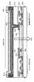
図2(A)はインバータ回路の断面構造図であり、図2(B)で示すインバータ回路の上面図のA−A' 断面構造を示している。尚、図2(C)に示すインバータ回路図における各端子部a、b、cは、インバータ回路の上面図に示す各端子と対応している。
【0067】
図1と図2では、nチャネル型TFTとpチャネル型TFTとを相補的に組み合わせて成るCMOS回路を例にして示したが、nチャネル型TFTを用いたNMOS回路や、液晶表示装置の画素部に本願発明を適用することもできる。
【0068】
[実施形態2]
本発明によれば、図3に示すように、LDD領域となる第2の不純物領域を、ゲート電極の第1層目302と重なる第2の不純物領域305a、306aとゲート電極と重ならない第2の不純物領域305b、306bとに分けることができる。すなわち、ゲート電極とオーバーラップするLDD領域と、オーバーラップしないLDD領域が形成される。この領域の作り分けは、フォトレジストによるマスクで容易に実施可能であり、第1の不純物添加の工程と、第1の不純物領域を形成する第2の不純物添加の工程により行われた。
【0069】
すなわち、図3(A)に示すLDD領域のそれぞれの長さX1、X2、およびY1、Y2の長さをある範囲で任意に設定することができる。ここで、nチャネル型TFTの信頼性を含めた特性を考慮すると、第1の不純物領域(ドレイン領域)308側に設けられる第2の不純物領域306a、306bは必須のものであったが、ゲート電極を挟んでその反対側に設けられる第2の不純物領域305a、305bは、nチャネル型TFTの動作環境を考慮して適宣設ければ良いものであった。
【0070】
これは、同一基板上に駆動電圧の異なる回路を作製するときにきわめて便利な方法であった。図3には、液晶表示装置のロジック回路部、バッファ回路部、アナログスイッチ部、および画素部に使用するTFTの設計値の一例を示す。このとき、それぞれのTFTの駆動電圧を考慮して、チャネル長はもとより、ゲート電極と重なる第2の不純物領域305a、306aとゲート電極と重ならない第2の不純物領域305b、306bの長さを設定することが可能となる。
【0071】
例えば、液晶表示装置のドライバ回路のロジック回路部TFTや、バッファ回路部のTFTは基本的にオン特性が重視されるので、いわゆるGOLD構造でも良く、ゲート電極と重ならない第2の不純物領域306bは必ずしも設ける必要はない。しかしあえて設ける場合は駆動電圧を考慮してX1の値を0.1〜4μm、代表的には0.5〜3μmの範囲で設定すれば良い。いずれにしても、耐圧を考慮してゲート電極と重ならない第2の不純物領域306bの値は、駆動電圧が高くなるにしたがって大きくすることが望ましい。また、このとき第1の不純物領域(ソース領域)307側には第2の不純物領域305a、305bをあえて設ける必要はなかった。
【0072】
また、サンプリング回路や、画素部に設けるTFTはオフ電流が増加しては困るので、例えば、チャネル長3μmとしてゲート電極と重なる第2の不純物領域305a、306aを1.5μmとし、ゲート電極と重ならない第2の不純物領域305b、306bを1.5μmとすれば良かった。勿論、本発明はここで示す設計値に限定されるものでなく、適宣決定すれば良いものである。
【0073】
以上のように、本発明において、ゲート電極の第1層目と、ゲート電極の第2層目とのチャネル長方向の長さは、作製するTFTの構造と深い関係があった。ゲート電極の第2層目のチャネル長方向の長さは、チャネル長Lにほぼ相当するものであった。このときLは0.1〜10μm、代表的には0.2〜5μmの値とすれば良かった。
【0074】
そして、第2の不純物領域305、306がゲート電極と重なる長さY1、Y2は、ゲート電極の第1層目302の長さと密接な関係にある。Y1、Y2の長さは、0.1〜4μm、代表的には0.5〜3μmで形成することが望ましい。また、第2の不純物領域305、306がゲート電極と重ならない長さX1、X2は、前述のように必ずしも設ける必要がない場合もあるが、通常は0.1〜3μm、代表的には0.3〜2μmとするのが良い。いずれにしても、TFTの動作状態を考慮して適宣決めると良い。
【0075】
nチャネル型TFTにおいてLDD領域は、第2の不純物領域306a、306bだけでも良い。また画素部のnチャネル型TFTのように、両極の電圧が印加されるような場合には、チャネル形成領域304を中心としてソース領域側307とドレイン領域側308の両方に設けることが望ましい。
【0076】
一方、pチャネル型TFTに対しては、チャネル形成領域304と、ソース領域307、ドレイン領域308だけを形成すれば良い。勿論、本発明のnチャネル型TFTと同様の構造としても良いが、pチャネル型TFTはもともと信頼性が高いため、オン電流を稼いでnチャネル型TFTとの特性バランスをとった方が好ましい。本願発明を図1に示すようにCMOS回路に適用する場合には、特にこの特性のバランスをとることが重要である。但し、本発明の構造をpチャネル型TFTに適用しても何ら問題はない。
【0077】
[実施例1]
本実施例では、本願発明の構成を図4〜図6を用い、画素部とその周辺に設けられる駆動回路の基本形態であるCMOS回路を同時に作製する方法について説明する。
【0078】
図4において、基板401には、例えばコーニング社の1737ガラス基板に代表される無アルカリガラス基板を用いた。そして、基板401のTFTが形成される表面に、下地膜402をプラズマCVD法やスパッタ法で形成した。下地膜402は図示していないが、窒化シリコン膜を25〜100nm、ここでは50nmの厚さに、酸化シリコン膜を50〜300nm、ここでは150nmの厚さに形成した。また、下地膜402は、窒化シリコン膜や窒化酸化シリコン膜のみを用いても良い。
【0079】
下地膜402は上記材料の1層で形成しても良いし、2層以上の積層構造としても良い。いずれにしてもその厚さが100〜300nm程度になるように形成する。例えば、プラズマCVD法でSiH4、NH3、N2Oから作製される第1の酸化窒化シリコン膜を10〜100nmの厚さに形成し、SiH4、N2Oから作製される第2の酸化窒化シリコン膜を100〜200nmの厚さに積層形成した2層構造として下地膜402を形成しても良い。
【0080】
次に、この下地膜402の上に50nmの厚さの、非晶質シリコン膜をプラズマCVD法で形成した。非晶質シリコン膜は含有水素量にもよるが、好ましくは400〜550℃で数時間加熱して脱水素処理を行い、含有水素量を5atom%以下として、結晶化の工程を行うことが望ましい。また、非晶質シリコン膜をスパッタ法や蒸着法などの他の作製方法で形成しても良いが、膜中に含まれる酸素、窒素などの不純物元素を十分低減させておくことが望ましい。
【0081】
ここで、下地膜と非晶質シリコン膜とはいずれもプラズマCVD法で作製されるものであり、このとき下地膜と非晶質シリコン膜を真空中で連続して形成しても良い。下地膜を形成後、一旦大気雰囲気にさらされない工程にすることにより、表面の汚染を防ぐことが可能となり、作製されるTFTの特性バラツキを低減させることができた。
【0082】
非晶質シリコン膜を結晶化する工程は、公知のレーザー結晶化技術または熱結晶化の技術を用いれば良い。本実施例では、パルス発振型のKrFエキシマレーザー光を線状に集光して非晶質シリコン膜に照射して結晶質シリコン膜を形成した。
【0083】
尚、本実施例では半導体層を非晶質シリコン膜から結晶質シリコン膜を形成したが、微結晶シリコン膜を用いても構わないし、直接結晶質シリコン膜を成膜しても良い。
【0084】
こうして形成された結晶質シリコン膜をパターニングして、島状の半導体層403、404、405を形成した。
【0085】
次に、島状の半導体層403、404、405を覆って、酸化シリコンまたは窒化シリコンを主成分とするゲート絶縁膜406を形成した。ゲート絶縁膜406は、プラズマCVD法でN2OとSiH4を原料とした窒化酸化シリコン膜を10〜200nm、好ましくは50〜150nmの厚さで形成すれば良い。ここでは100nmの厚さに形成した。
【0086】
そして、ゲート絶縁膜406の表面にゲート電極の第1層目となる第1の導電膜407と、ゲート電極の第2層目となる第2の導電膜408とを形成した。第1の導電膜407はSi、Geから選ばれた一種の元素、またはこれらの元素を主成分とする半導体膜で形成すれば良い。また、第1の導電膜407の厚さは5〜500nm、好ましくは10〜30nmとする必要がある。ここでは、20nmの厚さでSi膜を形成した。
【0087】
第1の導電膜として使用する半導体膜にはn型あるいはp型の導電型を付与する不純物元素が添加されていても良い。この半導体膜の作製法は公知の方法に従えば良く、例えば、減圧CVD法で基板温度を450〜500℃として、ジシラン(Si2H6)を250SCCM、ヘリウム(He)を300SCCM導入して作製することができる。このとき同時に、Si2H6に対してPH3を0.1〜2%混入させてn型の半導体膜を形成しても良い。
【0088】
ゲート電極の第2層目となる第2の導電膜は、Ti、Ta、W、Moから選ばれた元素、あるいはこれらの元素を主成分とする化合物で形成すば良い。これはゲート電極の電気抵抗を下げるために考慮されるものであり、例えば、Mo−W化合物を用いても良い。ここでは、Taを使用し、スパッタ法で、200〜1000nm、代表的には400nmの厚さに形成した。(図4(A))
【0089】
Ta膜を用いる場合には、同様にスパッタ法で形成することが可能である。Ta膜はスパッタガスにArを用いる。また、これらのスパッタガス中に適量のXeやKrを加えておくと、形成する膜の内部応力を緩和して膜の剥離を防止することができる。α相のTa膜の抵抗率は20μΩcm程度でありゲート電極に使用することができるが、β相のTa膜の抵抗率は180μΩcm程度でありゲート電極とするには不向きである。しかし、TaN膜はα相に近い結晶構造を持つので、この上にTa膜を形成すればα相のTa膜が容易に得られる。従って、Ta膜の成膜に先立って10〜50nmの厚さでTaN膜を形成しておいても良い。Ta膜は抵抗率を10〜50μΩcmの範囲ですることが好ましい。
【0090】
その他にW膜を用いることも可能であり、その場合はWをターゲットとしたスパッタ法で、アルゴン(Ar)ガスと窒素(N2)ガスを導入して導電層(A)をW膜で200nmの厚さに形成する。また、W膜を6フッ化タングステン(WF6)を用いて熱CVD法で形成することもできる。いずれにしてもゲート電極として使用するためには低抵抗化を図る必要があり、W膜の抵抗率は20μΩcm以下にすることが望ましい。W膜は結晶粒を大きくすることで低抵抗率化を図ることができるが、W膜中に酸素などの不純物元素が多い場合には結晶化が阻害され高抵抗化する。このことより、スパッタ法による場合、純度99.9999%のWターゲットを用い、さらに成膜時に気相中からの不純物の混入がないように十分配慮してW膜を形成することにより、抵抗率9〜20μΩcmを実現することができる。
【0091】
次に公知のパターニング技術を使ってレジストマスクを形成し、第2の導電膜408をエッチングしてゲート電極の第2層目を形成する工程を行った。第2の導電膜408はTa膜で形成されているので、ドライエッチング法により行った。ドライエッチングの条件として、Cl2を80SCCM導入して100mTorr、で500Wの高周波電力を投入して行った。そして、図4(B)に示すようにゲート電極の第2層目409、410、412、413と、配線411を形成した。ゲート電極の第2層目のチャネル長方向の長さは、CMOS回路を形成するゲート電極の第2層目409、410で3μmとし、また、画素部はマルチゲートの構造となっていて、ゲート電極の第2層目412、413の各々の長さを2μmとした。
【0092】
エッチング後わずかに残さが確認されたが、SPX洗浄液やEKCなどの溶液で洗浄することにより除去することができた。
【0093】
また、第2の導電膜408はウエットエッチング法で除去することもできた。例えば、Taの場合、フッ酸系のエッチング液で容易に除去することができた。
【0094】
また、画素TFTのドレイン側に保持容量を設ける構造となっている。このとき、第2の導電膜と同じ材料で保持容量の配線電極414が形成される。
【0095】
そして、n型を付与する第1の不純物元素を添加する工程を行った。この工程は第2の不純物領域を形成するための工程であった。ここでは、フォスフィン(PH3)を用いたイオンドープ法で行った。この工程では、ゲート絶縁膜406と第1の導電膜407を通してその下の半導体層にリンを添加するために、加速電圧は80keVと高めに設定した。半導体層に添加されるリンの濃度は、1×10¹⁶〜5×10¹⁹atoms/cm3(代表的には1×1017〜5×1018atoms/cm3)の範囲にするのが好ましく、ここでは1×1018atoms/cm3とした。そして、半導体層にリンが添加された領域415、416、417、418、419、420、421、422が形成された。(図4(B))
【0096】
このとき、第1の導電膜407で、ゲート電極の第2層目409、410、412、413と重ならない領域にもリンが添加された。この領域のリン濃度は特に規定されるものではないが、第1の導電膜の抵抗率を下げる効果が得られた。
【0097】
次にnチャネル型TFTを形成する領域をレジストマスク429、431で、配線が形成される領域をレジストマスク430で覆って、第1の導電膜407の一部を除去する工程を行った。ここでは、ドライエッチング法により行った。第1の導電膜407はSiであり、ドライエッチングの条件として、CF4を50SCCM、O2を45SCCM導入して50mTorr、で200Wの高周波電力を投入して行った。その結果、第1の導電膜434、423、435が残った。
【0098】
そして、pチャネル型TFTが形成される領域に、p型を付与する第3の不純物元素を添加するの工程を行った。ここではジボラン(B2H6)を用いてイオンドープ法で添加した。ここでも加速電圧を80keVとして、2×10²⁰atoms/cm3の濃度にボロンを添加した。そして、図4(C)に示すようにボロンが高濃度に添加された第3の不純物領域432、433が形成された。 (図4(C))
【0099】
さらに、レジストマスク429、430、431を完全に除去して、再度レジストマスク436、437、438、439、440、441を形成した。そして、レジストマスク436、439、440、441を用い、第1の導電膜をエッチングし、新たに第1の導電膜442、443、444、445を形成した。
【0100】
レジストマスク436は9μmの長さで、レジストマスク439、440は7μmの長さで形成した。その結果、n型を付与する第1の不純物添加の工程でリンが添加され、本工程でレジストマスク436、439、440で覆われた領域が、第2の不純物領域として画定した。
【0101】
そして、n型を付与する第2の不純物元素を添加する工程を行った。ここでは、フォスフィン(PH3)を用いたイオンドープ法で行った。この工程でも、ゲート絶縁膜306を通してその下の半導体層にリンを添加するために、加速電圧は80keVと高めに設定した。そして、リンが添加された領域446、447、448、449、450が形成された。この領域のリンの濃度はn型を付与する第1の不純物元素を添加する工程と比較して高濃度であり、1×10²⁰〜1×10²¹atoms/cm3とするのが好ましく、ここでは1×1020atoms/cm3とした。(図5(A))
【0102】
さらに、レジストマスク436、437、438、439、440、441を除去して新たにレジストマスク451、452、453、454、455、456を形成した。この工程において、nチャネル型TFTに形成されるレジストマスク451、454、455のチャネル長方向の長さはTFTの構造を決める上で重要であった。レジストマスク451、454、455は第1の導電膜442、443、444の一部を除去する目的で設けられるものであり、このレジストマスクの長さにより、第2の不純物領域がゲート電極と重なる領域と、重ならない領域をある範囲で自由に決めることができた。(図5(B))
【0103】
そして図5(C)に示すようにゲート電極の第1層目457、458、459、460が形成された。ここで、ゲート電極の第1層目457のチャネル長方向の長さは6μm、ゲート電極の第1層目458、459のチャネル長方向の長さは4μmとした。
【0104】
また、画素部には、保持容量部の電極460が形成された。
【0105】
図5(C)までの工程が終了したら、窒化シリコン膜461、第1の層間絶縁膜462を形成する工程を行った。最初に窒化シリコン膜461を50nmの厚さに成膜した。窒化シリコン膜461はプラズマCVD法で形成され、SiH4を5SCCM、NH3を40SCCM、N2を100SCCM導入して0.7Torr、300Wの高周波電力を投入した。そして、続いて第1の層間絶縁膜462として酸化シリコン膜をTEOSを500SCCM、O2を50SCCM導入し1Torr、200Wの高周波電力を投入して950nmの厚さに成膜した。
【0106】
そして、熱処理の工程を行った。熱処理の工程は、それぞれの濃度で添加されたn型またはp型を付与する不純物元素を活性化するために行う必要があった。この工程は、電気加熱炉を用いた熱アニール法や、前述のエキシマレーザーを用いたレーザーアニール法や、ハロゲンランプを用いたラピットサーマルアニール法(RTA法)で行えば良い。ここでは熱アニール法で活性化の工程を行った。加熱処理は、窒素雰囲気中において300〜700℃、好ましくは350〜550℃、ここでは450℃、2時間の処理を行った。
【0107】
第1の層間絶縁膜462と窒化シリコン膜461はその後、パターニングでそれぞれのTFTのソース領域と、ドレイン領域に達するコンタクトホールが形成された。そして、ソース電極463、464、465とドレイン電極467、468を形成した。図示していないが、本実施例ではこの電極を、Ti膜を100nm、Tiを含むAl膜300nm、Ti膜150nmをスパッタ法で連続して形成した3層構造の電極として用いた。
【0108】
そして、ソース電極463、464、465とドレイン電極467、468と、第1の層間絶縁膜462を覆ってパッシベーション膜469を形成した。パッシベーション膜469は、窒化シリコン膜で50nmの厚さで形成した。さらに、有機樹脂からなる第2の層間絶縁膜470を約1000nmの厚さに形成した。有機樹脂膜としては、ポリイミド、アクリル、ポリイミドアミド等を使用することができる。有機樹脂膜を用いることの利点は、成膜方法が簡単である点や、比誘電率が低いので、寄生容量を低減できる点、平坦性に優れる点などが上げられる。なお上述した以外の有機樹脂膜を用いることもできる。ここでは、基板に塗布後、熱重合するタイプのポリイミドを用い、300℃で焼成して形成した。
【0109】
以上の工程で、CMOS回路のnチャネル型TFTにはチャネル形成領域471、第1の不純物領域474、475、第2の不純物領域472、473が形成された。ここで、第2の不純物領域は、ゲート電極と重なる領域(GOLD領域)472a、473aが1.5μmの長さに、ゲート電極と重ならない領域(LDD領域)472b、473bが1.5μmの長さにそれぞれ形成された。そして、第1の不純物領域474はソース領域として、第1の不純物領域475はドレイン領域となった。
【0110】
pチャネル型TFTは、同様にクラッド構造のゲート電極が形成され、チャネル形成領域476、第3の不純物領域477、478が形成された。そして、第3の不純物領域477はソース領域として、第3の不純物領域478はドレイン領域となった。
【0111】
また、画素部のnチャネル型TFTはマルチゲートであり、チャネル形成領域479、484と第1の不純物領域482、483、487と第2の不純物領域480、481、485、486が形成された。ここで第2の不純物領域は、ゲート電極と重なる領域480a、481a、485a、486aと重ならない領域480b、481b、485b、486bとが形成された。
【0112】
こうして図6に示すように、基板401上にCMOS回路と、画素部が形成されたアクティブマトリクス基板が作製された。また、画素部のnチャネル型TFTのドレイン側には、保持容量部が同時に形成された。
【0113】
[実施例2]
本実施例では、実施例1と同じ工程で図5(A)に示す状態得た後、他の方法でゲート電極の第1層目の一部を除去する例を図7を用いて説明する。
【0114】
まず、図5(A)で形成したレジストマスク436、437、438、439、440、441をそのまま使用して、エッチングにより、第1のゲート導電膜442、443、444の一部を図7(A)に示すように除去した。
【0115】
ここでのエッチングの工程は、ゲート電極の第1層目がシリコン膜である場合、ドライエッチング法により、SF6を40SCCM、O2を10SCCM導入して、100mTorr、200Wの高周波電力を印加して行うことができた。
【0116】
このドライエッチングの条件では、下地にあるゲート絶縁膜との選択比は高く、ゲート絶縁膜406はほとんどエッチングされなかった。
【0117】
ここでは、レジストマスク436は、TFTのチャネル長方向に対して9μm、また、レジストマスク439、440は7μmの長さで形成されていた。そして、ここではドライエッチングにより第1の導電膜を1.5μmずつ除去して、ゲート電極の第1層目457、458、459、460を形成した。
【0118】
以降の工程は実施例1に従えば良く、図6に示すように窒化シリコン膜461、第1の層間絶縁膜462、ソース電極463、464、465、ドレイン電極467、468、パッシベーション膜469、第2の層間絶縁膜470を形成して、図4(C)に示すアクティブマトリクス基板が形成された。
【0119】
[実施例3]
本実施例では、実施例1と同じ工程で図5(A)に示す状態得た後、他の方法でゲート電極の第1層目の一部を除去する例を図8を用いて説明する。
【0120】
まず、図5(A)で形成したレジストマスク436、437、438、439、440、441を完全に除去して、再度フォトレジストを膜を形成し、裏面からの露光によるパターニングの工程を行った。このとき、図8(A)に示すようにゲート電極がマスクとなって、自己整合的にレジストマスク801、802、803、804、805、806が形成された。裏面からの露光は直接光と散乱光を利用して行うもので、光強度や露光時間などの露光条件の調節により、図8(A)に示すようにレジストマスクをゲート電極上の内側に形成することができた。
【0121】
但し、レジストマスク802、803はゲート電極410、配線411を保護するためのものであり、必ずしも必要なものでなく実施者が適宣設ければ良いものである。
【0122】
そして、ゲート電極の第1層目のマスクされていない領域をドライエッチング法により除去した。ドライエッチングの条件は実施例1と同様に行った。エッチングが終了した後レジストマスク801、802、803、804、805を除去した。
【0123】
以降の工程は実施例1に従えば良く、図6に示すように窒化シリコン膜461、第1の層間絶縁膜462、ソース電極463、464、465、ドレイン電極467、468、パッシベーション膜469、第2の層間絶縁膜470を形成して、図4(C)に示すアクティブマトリクス基板が形成された。
【0124】
[実施例4]
本実施例では、実施例1において半導体層として用いる結晶質半導体膜を、触媒元素を用いた熱結晶化法により形成する例を示す。触媒元素を用いる場合、特開平7−130652号公報、特開平8−78329号公報で開示された技術を用いることが望ましい。
【0125】
ここで、特開平7−130652号公報に開示されている技術を本願発明に適用する場合の例を図12に示す。まず基板1201に酸化シリコン膜1202を設け、その上に非晶質シリコン膜1203を形成した。さらに、重量換算で10ppmのニッケルを含む酢酸ニッケル塩溶液を塗布してニッケル含有層1204を形成した。(図12(A))
【0126】
次に、500℃、1時間の脱水素工程の後、500〜650℃で4〜12時間、例えば550℃、8時間の熱処理を行い、結晶質シリコン膜1205を形成した。こうして得られた結晶質シリコン膜1205は非常に優れた結晶質を有した。(図12(B))
【0127】
また、特開平8−78329号公報で開示された技術は、触媒元素を選択的に添加することによって、非晶質半導体膜の選択的な結晶化を可能としたものである。同技術を本願発明に適用した場合について、図13で説明する。
【0128】
まず、ガラス基板1301に酸化シリコン膜1302を設け、その上に非晶質シリコン膜1303、酸化シリコン膜1304を連続的に形成した。この時、酸化シリコン膜1304の厚さは150nmとした。
【0129】
次に酸化シリコン膜1304をパターニングして、選択的に開孔部1305を形成し、その後、重量換算で10ppmのニッケルを含む酢酸ニッケル塩溶液を塗布した。これにより、ニッケル含有層1306が形成され、ニッケル含有層1306は開孔部1305の底部のみで非晶質シリコン膜1302と接触した。(図13(A))
【0130】
次に、500〜650℃で4〜24時間、例えば570℃、14時間の熱処理を行い、結晶質シリコン膜1307を形成した。この結晶化の過程では、ニッケルが接した非晶質シリコン膜の部分が最初に結晶化し、そこから横方向へと結晶化が進行する。こうして形成された結晶質シリコン膜1307は棒状または針状の結晶が集合して成り、その各々の結晶は巨視的に見ればある特定の方向性をもって成長しているため、結晶性が揃っているという利点がある。(図13(B))
【0131】
尚、上記2つの技術において使用可能な触媒元素は、ニッケル(Ni)の以外にも、ゲルマニウム(Ge)、鉄(Fe)、パラジウム(Pd)、スズ(Sn)、鉛(Pb)、コバルト(Co)、白金(Pt)、銅(Cu)、金(Au)、といった元素を用いても良い。
【0132】
以上のような技術を用いて結晶質半導体膜(結晶質シリコン膜や結晶質シリコンゲルマニウム膜などを含む)を形成し、パターニングを行えば、結晶質TFTの半導体層を形成することができる。本実施例の技術を用いて、結晶質半導体膜から作製されたTFTは、優れた特性が得られるが、そのため高い信頼性を要求されてあいた。しかしながら、本願発明のTFT構造を採用することで、本実施例の技術を最大限に生かしたTFTを作製することが可能となった。
【0133】
[実施例5]
本実施例は、実施例1で用いられる半導体層を形成する方法として、非晶質半導体膜を初期膜として前記触媒元素を用いて結晶質半導体膜を形成した後で、その触媒元素を結晶質半導体膜から除去する工程を行った例を示す。本実施例ではその方法として、特開平10−247735、特開平10−135468号公報または特開平10−135469号公報に記載された技術を用いた。
【0134】
同公報に記載された技術は、非晶質半導体膜の結晶化に用いた触媒元素を結晶化後にリンのゲッタリング作用を用いて除去する技術である。同技術を用いることで、結晶質半導体膜中の触媒元素の濃度を1×10¹⁷atms/cm3以下、好ましくは1×1016atms/cm3にまで低減することができる。
【0135】
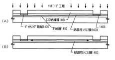
本実施例の構成について図14を用いて説明する。ここではコーニング社の1737基板に代表される無アルカリガラス基板を用いた。図14(A)では、実施例4で示した結晶化の技術を用いて、下地1402、結晶質シリコン膜1403が形成された状態を示している。そして、結晶質シリコン膜1403の表面にマスク用の酸化シリコン膜1404が150nmの厚さに形成され、パターニングにより開孔部が設けられ、結晶質シリコン膜を露出させた領域を設けてある。そして、リンを添加する工程を実施して、結晶質シリコン膜にリンが添加された領域1405が設けられた。
【0136】
この状態で、窒素雰囲気中で550〜800℃、5〜24時間、例えば600℃、12時間の熱処理を行うと、結晶質シリコン膜にリンが添加された領域1405がゲッタリングサイトとして働き、結晶質シリコン膜1403に残存していた触媒元素はリンが添加された領域1405に偏析させることができた。
【0137】
そして、マスク用の酸化シリコン膜1404と、リンが添加された領域1405とをエッチングして除去することにより、結晶化の工程で使用した触媒元素の濃度を1×10¹⁷atms/cm3以下にまで低減された結晶質シリコン膜を得ることができた。この結晶質シリコン膜はそのまま実施例1で示した本願発明のTFTの半導体層として使用することができた。
【0138】
[実施例6]
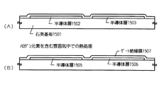
本実施例では、実施例1で示した本願発明のTFTを作製する工程において、半導体層とゲート絶縁膜を形成する他の実施形態を示す。そして、本実施例の構成を図15で説明する。
【0139】
ここでは、少なくとも700〜1100℃程度の耐熱性を有する基板が必要であり、石英基板1501が用いられた。そして実施例4及び実施例5で示した技術を用い、結晶質半導体が形成され、これをTFTの半導体層にするために、島状にパターニングして半導体層1502、1503を形成した。そして、半導体層1502、1503を覆って、ゲート絶縁膜1504を酸化シリコンを主成分とする膜で形成した。本実施例では、プラズマCVD法で窒化酸化シリコン膜を70nmの厚さで形成した。(図15(A))
【0140】
そして、ハロゲン(代表的には塩素)と酸素を含む雰囲気中で熱処理を行った。本実施例では、950℃、30分とした。尚、処理温度は700〜1100℃の範囲で選択すれば良く、処理時間も10分から8時間の間で選択すれば良かった。(図15(B))
【0141】
その結果、本実施例の条件では、半導体層1502、1503とゲート絶縁膜1504との界面で熱酸化膜が形成され、ゲート絶縁膜1507が形成された。また、ハロゲン雰囲気での酸化の過程で、ゲート絶縁膜1504と半導体層1502、1503に含まれる不純物で、特に金属不純物元素はハロゲンと化合物を形成し、気相中に除去することができた。
【0142】
以上の工程で作製されたゲート絶縁膜1507は、絶縁耐圧が高く半導体層1505、1506とゲート絶縁膜1507の界面は非常に良好なものであった。本願発明のTFTの構成を得るためには、以降の工程は実施例1に従えば良かった。
【0143】
[実施例7]
本実施例では、実施例4で示した方法で結晶質半導体膜を形成し、実施例1で示す工程でアクティブマトリクス基板を作製方法において、結晶化の工程で使用した触媒元素をゲッタリングにより除去する例を示す。まず、実施例1において、図4(A)で示される半導体層403、404、405は、触媒元素を用いて作製された結晶質シリコン膜であった。このとき、結晶化の工程で用いられた触媒元素が半導体層中に残存するので、ゲッタリングの工程を実施することが望ましかった。
【0144】
ここでは、図4(C)に示す工程までそのまま実施した。そして、レジストマスク429、430、431を除去した。
【0145】
そして、図16に示すように、新たなレジストマスク1601、1602、1603、1604、1605、1606を形成した。そして、n型を付与する第2の不純物添加の工程を行った。そして、半導体層にリンが添加された領域1611、1612、1613、1614、1615、1616、1617が形成された。
【0146】
ここで、リンが添加された領域1613、1614にはすでにp型を付与する不純物元素であるボロンが添加されているが、このときリン濃度は1×10²⁰〜1×10²¹atoms/cm3であり、ボロンに対して1/2程度の濃度で添加されるので、pチャネル型TFTの特性には何ら影響を及ぼさなかった。
【0147】
この状態で、窒素雰囲気中で400〜800℃、1〜24時間、例えば600℃、12時間の加熱処理の工程を行った。この工程により、添加されたn型及びp型を付与する不純物元素を活性化することができた。さらに、前記リンが添加されている領域がゲッタリングサイトとなり、結晶化の工程の後残存していた触媒元素を偏析させることができた。その結果、チャネル形成領域から触媒元素を除去することができた。(図16(B))
【0148】
図16(B)の工程が終了したら、以降の工程は実施例1の工程に従い、図6状態を形成することにより、アクティブマトリクス基板を作製することができた。
【0149】
[実施例8]
本実施例では、実施例1で作製されたアクティブマトリクス基板から、アクティブマトリクス型液晶表示装置を作製する工程を説明する。
【0150】
図6の状態のアクティブマトリクス基板に対して、図11(A)に示すように遮光膜1101、第3の層間絶縁膜1102を形成した。遮光膜1101は顔料を含む有機樹脂膜や、Ti、Crなどの金属膜を用いると良い。また、第3の層間絶縁膜1102は、ポリイミドなどの有機樹脂膜で形成した。そして、第3の層間絶縁膜1102と第2の層間絶縁膜470、パッシベーション膜469にドレイン電極468に達するコンタクトホールを形成し、画素電極1103を形成した。画素電極1103は、透過型液晶表示装置とする場合には透明導電膜を用い、反射型の液晶表示装置とする場合には金属膜を用いれば良い。ここでは透過型の液晶表示装置とするために、酸化インジウム・スズ(ITO)膜を100nmの厚さにスパッタ法で形成し、画素電極1103を形成した。
【0151】
透明導電膜の材料のエッチング処理は塩酸系の溶液により行う。しかし、ITOのエッチングは残渣が発生しやすいので、エッチング加工性を改善するために酸化インジウム酸化亜鉛合金(In2O3―ZnO)を用いても良い。酸化インジウム酸化亜鉛合金は表面平滑性に優れ、ITOと比較して熱安定性にも優れているという特徴をもつ。同様に、酸化亜鉛(ZnO)も適した材料であり、さらに可視光の透過率や導電率を高めるためにガリウム(Ga)を添加した酸化亜鉛(ZnO:Ga)などを用いることができる。
【0152】
次に、図11(B)に示すように、配向膜1104を第3の層間絶縁膜1102と画素電極1103形成する。通常液晶表示素子の配向膜にはポリイミド樹脂が多く用いられている。対向側の基板1105には、透明導電膜1106と、配向膜1107とを形成した。配向膜は形成された後、ラビング処理を施して液晶分子がある一定のプレチルト角を持って平行配向するようにした。
【0153】
上記の工程を経て、画素部と、CMOS回路が形成されたアクティブマトリクス基板と対向基板とを、公知のセル組み工程によってシール材やスペーサ(共に図示せず)などを介して貼りあわせる。その後、両基板の間に液晶材料1108を注入し、封止剤(図示せず)によって完全に封止した。よって図11(B)に示すアクティブマトリクス型液晶表示装置が完成した。
【0154】
次に本実施例のアクティブマトリクス型液晶表示装置の構成を、図9と図10を用いて説明する。図9は本実施例のアクティブマトリクス基板の斜視図である。アクティブマトリクス基板は、ガラス基板401上に形成された、画素部901と、走査(ゲート)線駆動回路902と、信号(ソース)線駆動回路903で構成される。画素部の画素TFT900はnチャネル型TFTであり、周辺に設けられる駆動回路はCMOS回路を基本として構成されている。走査(ゲート)線駆動回路902と、信号(ソース)線駆動回路903はそれぞれゲート配線1002とソース配線1003で画素部901に接続されている。
【0155】
図10(A)は画素部901の上面図であり、ほぼ1画素の上面図である。画素部にはnチャネル型TFTが設けられている。ゲート配線1002に連続して形成されるゲート電極1020は、図示されていないゲート絶縁膜を介してその下の半導体層1001と交差している。図示はしていないが、半導体層には、ソース領域、ドレイン領域、第1の不純物領域が形成されている。また、画素TFTのドレイン側には、半導体層と、ゲート絶縁膜と、第1及びゲート電極の第2層目と同じ材料で形成された電極とから、保持容量1007が形成されている。そして、保持容量1007に接続した容量配線1021が、ゲート配線1002と平行に設けられている。また、図10(A)で示すA―A‘に沿った断面構造は、図6に示す画素部の断面図に対応している。
【0156】
一方、図10(B)に示すCMOS回路では、ゲート配線1010から延在するゲート電極409、410が、図示されていないゲート絶縁膜を介してその下の半導体層403、404とそれぞれ交差している。図示はしていないが、同様にnチャネル型TFTの半導体層には、ソース領域、ドレイン領域、第1の不純物領域が形成されている。また、pチャネル型TFTの半導体層にはソース領域とドレイン領域が形成されている。そして、その位置関係は、B―B‘に沿った断面構造は、図6に示す画素部の断面図に対応している。
【0157】
本実施例では、画素TFT900をダブルゲートの構造としているが、シングルゲートの構造でも良いし、トリプルゲートとしたマルチゲート構造にしても構わない。本実施例のアクティブマトリクス基板の構造は、本実施例の構造に限定されるものではない。本願発明の構造は、ゲート電極の構造と、ゲート絶縁膜を介して設けられた半導体層のソース領域と、ドレイン領域と、その他の不純物領域の構成に特徴があるので、それ以外の構成については実施者が適宣決定すれば良い。
【0158】
[実施例9]
図17は、実施例8で示したアクティブマトリクス型液晶表示装置の回路構成の一例を示す。本実施例のアクティブマトリクス型液晶表示装置は、ソース信号線側駆動回路1701、ゲート信号線側駆動回路(A)1707、ゲート信号線側駆動回路(B)1711、プリチャージ回路1712、画素部1706を有している。
【0159】
ソース信号線側駆動回路1701は、シフトレジスタ回路1702、レベルシフタ回路1703、バッファ回路1704、サンプリング回路1705を備えている。
【0160】
また、ゲート信号線側駆動回路(A)1707は、シフトレジスタ回路1708、レベルシフタ回路1709、バッファ回路1710を備えている。ゲート信号線側駆動回路(B)1711も同様な構成である。
【0161】
ここで、それぞれの回路の駆動電圧の一例を示すと、シフトレジスタ回路1702、1708は10〜16Vであり、レベルシフタ回路1703、1709、バッファ回路1704、1710、サンプリング回路1705画素部1706は14〜16Vであった。サンプリング回路1705画素部1706は印加される電圧の振幅であり、通常極性反転された電圧が交互に印加されていた。
【0162】
本発明は、nチャネル型TFTの駆動電圧を考慮して、LDD領域となる第2の不純物領域の長さを同一基板上で異ならしめることが容易であり、それぞれの回路を構成するTFTに対して、最適な形状を同一工程で作り込むことができた。
【0163】
図18(A)はシフトレジスタ回路のTFTの構成例を示している。シフトレジスタ回路のnチャネル型TFTはシングルゲートであり、ドレイン側にのみLDD領域となる第2の不純物領域が設けられている。ここで、ゲート電極とオーバーラップするLDD領域(GOLD領域)1803aとオーバーラップしないLDD領域1803bの長さは、例えば、図3(C)に従えば良く、1803aを2.0μm、1803bを1.0μmとして形成することができる。
【0164】
図18(B)はレベルシフタ回路、バッファ回路のTFTの構成例を示している。これらの回路のnチャネル型TFTはダブルゲートとしてあり、ドレイン側にLDD領域となる第2の不純物領域が設けられている。例えば、ゲート電極とオーバーラップするLDD領域(GOLD領域)1812a、1813aの長さを2.5μmとし、オーバーラップしないLDD領域1812b、1813bの長さはを2.5μmとすることができる。
【0165】
図18(C)はサンプリング回路のTFTの構成例を示している。この回路のnチャネル型TFTはシングルゲートであるが、極性反転されるために、ソース側およびドレイン側の両方にLDD領域となる第2の不純物領域が設けられている。ゲート電極とオーバーラップするLDD領域(GOLD領域)1814aと1815a、及びオーバーラップしないLDD領域1814bと1815bの長さは、それぞれ等しくすることが好ましく、例えば、ゲート電極とオーバーラップするLDD領域(GOLD領域)1814aと1815aを1.5μm、オーバーラップしないLDD領域1814bと1815bの長さを1.0μmとすることができる。
【0166】
図18(D)は画素部の構成例を示している。この回路のnチャネル型TFTはマルチゲートであるが、極性反転されるために、ソース側およびドレイン側の両方にLDD領域となる第2の不純物領域が設けられている。例えば、ゲート電極とオーバーラップするLDD領域(GOLD領域)1816aと1817aを1.5μm、オーバーラップしないLDD領域1816bと1816bの長さを1.5μmとすることができる。
【0167】
[実施例10]
本実施例では、本願発明を用いてEL(エレクトロルミネッセンス)表示装置を作製した例について説明する。
【0168】
図32(A)は本願発明を用いたEL表示装置の上面図である。図32(A)において、4010は基板、4011は画素部、4012はソース側駆動回路、4013はゲート側駆動回路であり、それぞれの駆動回路は配線4014〜4016を経てFPC4017に至り、外部機器へと接続される。
【0169】
このとき、少なくとも画素部、好ましくは駆動回路及び画素部を囲むようにしてカバー材6000、シーリング材(ハウジング材ともいう)7000、密封材(第2のシーリング材)7001が設けられている。
【0170】
また、図32(B)は本実施例のEL表示装置の断面構造であり、基板4010、下地膜4021の上に駆動回路用TFT(但し、ここではnチャネル型TFTとpチャネル型TFTを組み合わせたCMOS回路を図示している。)4022及び画素部用TFT4023(但し、ここではEL素子への電流を制御するTFTだけ図示している。)が形成されている。
【0171】
本願発明は、駆動回路用TFT4022、画素部用TFT4023に際して用いることができる。
【0172】
本願発明を用いて駆動回路用TFT4022、画素部用TFT4023が完成したら、樹脂材料でなる層間絶縁膜(平坦化膜)4026の上に画素部用TFT4023のドレインと電気的に接続する透明導電膜でなる画素電極4027を形成する。画素電極4027が透明導電膜である場合、画素部用TFTとしては、pチャネル型TFTを用いることが好ましい。透明導電膜としては、酸化インジウムと酸化スズとの化合物(ITOと呼ばれる)または酸化インジウムと酸化亜鉛との化合物を用いることができる。そして、画素電極4027を形成したら、絶縁膜4028を形成し、画素電極4027上に開口部を形成する。
【0173】
次に、EL層4029を形成する。EL層4029は公知のEL材料(正孔注入層、正孔輸送層、発光層、電子輸送層または電子注入層)を自由に組み合わせて積層構造または単層構造とすれば良い。どのような構造とするかは公知の技術を用いれば良い。また、EL材料には低分子系材料と高分子系(ポリマー系)材料がある。低分子系材料を用いる場合は蒸着法を用いるが、高分子系材料を用いる場合には、スピンコート法、印刷法またはインクジェット法等の簡易な方法を用いることが可能である。
【0174】
本実施例では、シャドーマスクを用いて蒸着法によりEL層を形成する。シャドーマスクを用いて画素毎に波長の異なる発光が可能な発光層(赤色発光層、緑色発光層及び青色発光層)を形成することで、カラー表示が可能となる。その他にも、色変換層(CCM)とカラーフィルターを組み合わせた方式、白色発光層とカラーフィルターを組み合わせた方式があるがいずれの方法を用いても良い。勿論、単色発光のEL表示装置とすることもできる。
【0175】
EL層4029を形成したら、その上に陰極4030を形成する。陰極4030とEL層4029の界面に存在する水分や酸素は極力排除しておくことが望ましい。従って、真空中でEL層4029と陰極4030を連続成膜するか、EL層4029を不活性雰囲気で形成し、大気解放しないで陰極4030を形成するといった工夫が必要である。本実施例ではマルチチャンバー方式(クラスターツール方式)の成膜装置を用いることで上述のような成膜を可能とする。
【0176】
なお、本実施例では陰極4030として、LiF(フッ化リチウム)膜とAl(アルミニウム)膜の積層構造を用いる。具体的にはEL層4029上に蒸着法で1nm厚のLiF(フッ化リチウム)膜を形成し、その上に300nm厚のアルミニウム膜を形成する。勿論、公知の陰極材料であるMgAg電極を用いても良い。そして陰極4030は4031で示される領域において配線4016に接続される。配線4016は陰極4030に所定の電圧を与えるための電源供給線であり、導電性ペースト材料4032を介してFPC4017に接続される。
【0177】
4031に示された領域において陰極4030と配線4016とを電気的に接続するために、層間絶縁膜4026及び絶縁膜4028にコンタクトホールを形成する必要がある。これらは層間絶縁膜4026のエッチング時(画素電極用コンタクトホールの形成時)や絶縁膜4028のエッチング時(EL層形成前の開口部の形成時)に形成しておけば良い。また、絶縁膜4028をエッチングする際に、層間絶縁膜4026まで一括でエッチングしても良い。この場合、層間絶縁膜4026と絶縁膜4028が同じ樹脂材料であれば、コンタクトホールの形状を良好なものとすることができる。
【0178】
このようにして形成されたEL素子の表面を覆って、パッシベーション膜6003、充填材6004、カバー材6000が形成される。
【0179】
さらに、EL素子部を囲むようにして、カバー材7000と基板4010の内側にシーリング材が設けられ、さらにシーリング材7000の外側には密封材(第2のシーリング材)7001が形成される。
【0180】
このとき、この充填材6004は、カバー材6000を接着するための接着剤としても機能する。充填材6004としては、PVC(ポリビニルクロライド)、エポキシ樹脂、シリコーン樹脂、PVB(ポリビニルブチラル)またはEVA(エチレンビニルアセテート)を用いることができる。この充填材6004の内部に乾燥剤を設けておくと、吸湿効果を保持できるので好ましい。
【0181】
また、充填材6004の中にスペーサーを含有させてもよい。このとき、スペーサーをBaOなどからなる粒状物質とし、スペーサー自体に吸湿性をもたせてもよい。
【0182】
スペーサーを設けた場合、パッシベーション膜6003はスペーサー圧を緩和することができる。また、パッシベーション膜とは別に、スペーサー圧を緩和する樹脂膜などを設けてもよい。
【0183】
また、カバー材6000としては、ガラス板、アルミニウム板、ステンレス板、FRP(Fiberglass−Reinforced Plastics)板、PVF(ポリビニルフルオライド)フィルム、マイラーフィルム、ポリエステルフィルムまたはアクリルフィルムを用いることができる。なお、充填材6004としてPVBやEVAを用いる場合、数十μmのアルミニウムホイルをPVFフィルムやマイラーフィルムで挟んだ構造のシートを用いることが好ましい。
【0184】
但し、EL素子からの発光方向(光の放射方向)によっては、カバー材6000が透光性を有する必要がある。
【0185】
また、配線4016はシーリング材7000および密封材7001と基板4010との隙間を通ってFPC4017に電気的に接続される。なお、ここでは配線4016について説明したが、他の配線4014、4015も同様にしてシーリング材7000および密封材7001の下を通ってFPC4017に電気的に接続される。
【0186】
さらに異なる形態のEL表示装置を作製した例について、図33(A)、(B)を用いて説明する。図32(A)、(B)と同じ番号のものは同じ部分を指しているので説明は省略する。
【0187】
図33(A)は本実施例のEL表示装置の上面図であり、図33(A)をA-A'で切断した断面図を図33(B)に示す。
【0188】
図32で示したものと同様にして、EL素子の表面を覆ってパッシベーション膜6003までを形成する。
【0189】
さらに、EL素子を覆うようにして充填材6004を設ける。この充填材6004は、カバー材6000を接着するための接着剤としても機能する。充填材6004としては、PVC(ポリビニルクロライド)、エポキシ樹脂、シリコーン樹脂、PVB(ポリビニルブチラル)またはEVA(エチレンビニルアセテート)を用いることができる。この充填材6004の内部に乾燥剤を設けておくと、吸湿効果を保持できるので好ましい。
【0190】
また、充填材6004の中にスペーサーを含有させてもよい。このとき、スペーサーをBaOなどからなる粒状物質とし、スペーサー自体に吸湿性をもたせてもよい。
【0191】
スペーサーを設けた場合、パッシベーション膜6003はスペーサー圧を緩和することができる。また、パッシベーション膜とは別に、スペーサー圧を緩和する樹脂膜などを設けてもよい。
【0192】
また、カバー材6000としては、ガラス板、アルミニウム板、ステンレス板、FRP(Fiberglass−Reinforced Plastics)板、PVF(ポリビニルフルオライド)フィルム、マイラーフィルム、ポリエステルフィルムまたはアクリルフィルムを用いることができる。なお、充填材6004としてPVBやEVAを用いる場合、数十μmのアルミニウムホイルをPVFフィルムやマイラーフィルムで挟んだ構造のシートを用いることが好ましい。
【0193】
但し、EL素子からの発光方向(光の放射方向)によっては、カバー材6000が透光性を有する必要がある。
【0194】
次に、充填材6004を用いてカバー材6000を接着した後、充填材6004の側面(露呈面)を覆うようにフレーム材6001を取り付ける。フレーム材6001はシーリング材(接着剤として機能する)6002によって接着される。このとき、シーリング材6002としては、光硬化性樹脂を用いるのが好ましいが、EL層の耐熱性が許せば熱硬化性樹脂を用いても良い。なお、シーリング材6002はできるだけ水分や酸素を透過しない材料であることが望ましい。また、シーリング材6002の内部に乾燥剤を添加してあっても良い。
【0195】
また、配線4016はシーリング材6002と基板4010との隙間を通ってFPC4017に電気的に接続される。なお、ここでは配線4016について説明したが、他の配線4014、4015も同様にしてシーリング材6002の下を通ってFPC4017に電気的に接続される。
【0196】
EL表示装置の画素部の詳細な断面構造を図34に、上面構造を図35(A)に、回路図を図35(B)に示す。図34、図35(A)及び図35(B)では共通の符号を用いるので互いに参照すれば良い。
【0197】
図34において、基板3001上に設けられたスイッチング用TFT3002は本発明のnチャネル型TFTを用いて形成される(実施例1〜7参照)。本実施例ではダブルゲート構造としているが、構造及び作製プロセスに大きな違いはないので説明は省略する。但し、ダブルゲート構造とすることで実質的に二つのTFTが直列された構造となり、オフ電流値を低減することができるという利点がある。なお、本実施例ではダブルゲート構造としているが、シングルゲート構造でも構わないし、トリプルゲート構造やそれ以上のゲート本数を持つマルチゲート構造でも構わない。また、本願発明のpチャネル型TFTを用いて形成しても構わない。
【0198】
また、電流制御用TFT3003は本発明のnチャネル型TFTを用いて形成される。このとき、スイッチング用TFT3002のドレイン配線3035は配線3036によって電流制御用TFTのゲート電極3037に電気的に接続されている。また、3038で示される配線は、スイッチング用TFT3002のゲート電極3039a、3039bを電気的に接続するゲート配線である。
【0199】
このとき、電流制御用TFT3003が本発明の構造であることは非常に重要な意味を持つ。電流制御用TFTはEL素子を流れる電流量を制御するための素子であるため、多くの電流が流れ、熱による劣化やホットキャリアによる劣化の危険性が高い素子でもある。そのため、電流制御用TFTのドレイン側に、ゲート絶縁膜を介してゲート電極に重なるようにGOLD領域(第2の不純物領域)を設ける本発明の構造は極めて有効である。
【0200】
また、本実施例では電流制御用TFT3003をシングルゲート構造で図示しているが、複数のTFTを直列につなげたマルチゲート構造としても良い。さらに、複数のTFTを並列につなげて実質的にチャネル形成領域を複数に分割し、熱の放射を高い効率で行えるようにした構造としても良い。このような構造は熱による劣化対策として有効である。
【0201】
また、図35(A)に示すように、電流制御用TFT3003のゲート電極3037となる配線は3004で示される領域で、電流制御用TFT3003のドレイン配線3040と絶縁膜を介して重なる。このとき、3004で示される領域ではコンデンサが形成される。このコンデンサ3004は電流制御用TFT3003のゲートにかかる電圧を保持するためのコンデンサとして機能する。なお、ドレイン配線3040は電流供給線(電源線)3006に接続され、常に一定の電圧が加えられている。
【0202】
スイッチング用TFT3002及び電流制御用TFT3003の上には第1パッシベーション膜3041が設けられ、その上に樹脂絶縁膜でなる平坦化膜3042が形成される。平坦化膜3042を用いてTFTによる段差を平坦化することは非常に重要である。後に形成されるEL層は非常に薄いため、段差が存在することによって発光不良を起こす場合がある。従って、EL層をできるだけ平坦面に形成しうるように画素電極を形成する前に平坦化しておくことが望ましい。
【0203】
また、3043は反射性の高い導電膜でなる画素電極(EL素子の陰極)であり、電流制御用TFT3003のドレインに電気的に接続される。この場合においては、電流制御用TFTとしてnチャネル型TFTを用いることが好ましい。画素電極3043としてはアルミニウム合金膜、銅合金膜または銀合金膜など低抵抗な導電膜またはそれらの積層膜を用いることが好ましい。勿論、他の導電膜との積層構造としても良い。
【0204】
また、絶縁膜(好ましくは樹脂)で形成されたバンク3044a、3044bにより形成された溝(画素に相当する)の中に発光層3045が形成される。なお、ここでは一画素しか図示していないが、R(赤)、G(緑)、B(青)の各色に対応した発光層を作り分けても良い。発光層とする有機EL材料としてはπ共役ポリマー系材料を用いる。代表的なポリマー系材料としては、ポリパラフェニレンビニレン(PPV)系、ポリビニルカルバゾール(PVK)系、ポリフルオレン系などが挙げられる。
【0205】
なお、PPV系有機EL材料としては様々な型のものがあるが、例えば「H. Shenk,H.Becker,O.Gelsen,E.Kluge,W.Kreuder,and H.Spreitzer,“Polymers for Light Emitting Diodes”,Euro Display,Proceedings,1999,p.33-37」や特開平10−92576号公報に記載されたような材料を用いれば良い。
【0206】
具体的な発光層としては、赤色に発光する発光層にはシアノポリフェニレンビニレン、緑色に発光する発光層にはポリフェニレンビニレン、青色に発光する発光層にはポリフェニレンビニレン若しくはポリアルキルフェニレンを用いれば良い。膜厚は30〜150nm(好ましくは40〜100nm)とすれば良い。
【0207】
但し、以上の例は発光層として用いることのできる有機EL材料の一例であって、これに限定する必要はまったくない。発光層、電荷輸送層または電荷注入層を自由に組み合わせてEL層(発光及びそのためのキャリアの移動を行わせるための層)を形成すれば良い。
【0208】
例えば、本実施例ではポリマー系材料を発光層として用いる例を示したが、低分子系有機EL材料を用いても良い。また、電荷輸送層や電荷注入層として炭化珪素等の無機材料を用いることも可能である。これらの有機EL材料や無機材料は公知の材料を用いることができる。
【0209】
本実施例では発光層3045の上にPEDOT(ポリチオフェン)またはPAni(ポリアニリン)でなる正孔注入層3046を設けた積層構造のEL層としている。そして、正孔注入層3046の上には透明導電膜でなる陽極3047が設けられる。本実施例の場合、発光層3045で生成された光は上面側に向かって(TFTの上方に向かって)放射されるため、陽極は透光性でなければならない。透明導電膜としては酸化インジウムと酸化スズとの化合物や酸化インジウムと酸化亜鉛との化合物を用いることができるが、耐熱性の低い発光層や正孔注入層を形成した後で形成するため、可能な限り低温で成膜できるものが好ましい。
【0210】
陽極3047まで形成された時点でEL素子3005が完成する。なお、ここでいうEL素子3005は、画素電極(陰極)3043、発光層3045、正孔注入層3046及び陽極3047で形成されたコンデンサを指す。図35(A)に示すように画素電極3043は画素の面積にほぼ一致するため、画素全体がEL素子として機能する。従って、発光の利用効率が非常に高く、明るい画像表示が可能となる。
【0211】
ところで、本実施例では、陽極3047の上にさらに第2パッシベーション膜3048を設けている。第2パッシベーション膜3048としては窒化珪素膜または窒化酸化珪素膜が好ましい。この目的は、外部とEL素子とを遮断することであり、有機EL材料の酸化による劣化を防ぐ意味と、有機EL材料からの脱ガスを抑える意味との両方を併せ持つ。これによりEL表示装置の信頼性が高められる。
【0212】
以上のように本願発明のEL表示パネルは図34のような構造の画素からなる画素部を有し、オフ電流値の十分に低いスイッチング用TFTと、ホットキャリア注入に強い電流制御用TFTとを有する。従って、高い信頼性を有し、且つ、良好な画像表示が可能なEL表示パネルが得られる。
【0213】
なお、図34の構成は、実施例1〜7構成と自由に組み合わせて実施することが可能である。また、実施例12の電子機器の表示部として本実施例のEL表示装置を用いることは有効である。
【0214】
また、画素部の他の構成として、EL素子3005の構造を反転させた構造について説明する。説明には図36を用いる。なお、図34の構造と異なる点はEL素子の部分と電流制御用TFTだけであるので、その他の説明は省略することとする。
【0215】
図36において、電流制御用TFT3103は本発明のpチャネル型TFTを用いて形成される。作製プロセスは実施例1〜7を参照すれば良い。
【0216】
図36では、画素電極(陽極)3050として透明導電膜を用いる。具体的には酸化インジウムと酸化亜鉛との化合物でなる導電膜を用いる。勿論、酸化インジウムと酸化スズとの化合物でなる導電膜を用いても良い。
【0217】
そして、絶縁膜でなるバンク3051a、3051bが形成された後、溶液塗布によりポリビニルカルバゾールでなる発光層3052が形成される。その上にはカリウムアセチルアセトネート(acacKと表記される)でなる電子注入層3053、アルミニウム合金でなる陰極3054が形成される。この場合、陰極3054がパッシベーション膜としても機能する。こうしてEL素子3101が形成される。
【0218】
発光層3052で発生した光は、矢印で示されるようにTFTが形成された基板の方に向かって放射される。
【0219】
なお、図36の構成は、実施例1〜7の構成と自由に組み合わせて実施することが可能である。また、実施例12の電子機器の表示部として本実施例のEL表示パネルを用いることは有効である。
【0220】
図35(B)に示した回路図とは異なる構造の画素とした場合の例について図21(A)〜(C)に示す。なお、本実施例において、3201はスイッチング用TFT3202のソース配線、3203はスイッチング用TFT3202のゲート配線、3204は電流制御用TFT、3205はコンデンサ、3206、3208は電流供給線、3207はEL素子とする。
【0221】
図21(A)は、二つの画素間で電流供給線3206を共通とした場合の例である。即ち、二つの画素が電流供給線3206を中心に線対称となるように形成されている点に特徴がある。この場合、電源供給線の本数を減らすことができるため、画素部をさらに高精細化することができる。
【0222】
また、図21(B)は、電流供給線3208をゲート配線3203と平行に設けた場合の例である。なお、図21(B)では電流供給線3208とゲート配線3203とが重ならないように設けた構造となっているが、両者が異なる層に形成される配線であれば、絶縁膜を介して重なるように設けることもできる。この場合、電源供給線3208とゲート配線3203とで専有面積を共有させることができるため、画素部をさらに高精細化することができる。
【0223】
また、図21(C)は、図21(B)の構造と同様に電流供給線3208をゲート配線3203a、3203bと平行に設け、さらに、二つの画素を電流供給線3208を中心に線対称となるように形成する点に特徴がある。また、電流供給線3208をゲート配線3203a、3203bのいずれか一方と重なるように設けることも有効である。この場合、電源供給線の本数を減らすことができるため、画素部をさらに高精細化することができる。
【0224】
なお、図21で示す回路の構成は、実施例1〜7の構成と自由に組み合わせて実施することが可能である。また、実施例12の電子機器の表示部として本実施例の画素構造を有するEL表示表示装置を用いることは有効である。
【0225】
図35(A)、(B)では電流制御用TFT3003のゲートにかかる電圧を保持するためにコンデンサ3004を設ける構造としているが、コンデンサ3004を省略することも可能である。電流制御用TFT3003として実施例1〜7に示すような本発明のnチャネル型TFTを用いているため、ゲート絶縁膜を介してゲート電極に重なるように設けられたGOLD領域(第2の不純物領域)を有している。この重なり合った領域には一般的にゲート容量と呼ばれる寄生容量が形成されるが、本実施例ではこの寄生容量をコンデンサ3004の代わりとして積極的に用いる点に特徴がある。
【0226】
この寄生容量のキャパシタンスは、上記ゲート電極とGOLD領域とが重なり合った面積によって変化するため、その重なり合った領域に含まれるGOLD領域の長さによって決まる。
【0227】
また、図21(A)、(B)、(C)の構造においても同様に、コンデンサ3205を省略することは可能である。
【0228】
なお、このような構成は、実施例1〜7の構成と自由に組み合わせて実施することが可能である。また、実施例12の電子機器の表示部として本実施例の画素構造を有するEL表示装置を用いることは有効である。
【0229】
[実施例11]
上述の本発明の液晶表示装置にはネマチック液晶以外にも様々な液晶を用いることが可能である。例えば、1998, SID, "Characteristics and Driving Scheme of Polymer-Stabilized Monostable FLCD Exhibiting Fast Response Time and High Contrast Ratio with Gray-Scale Capability" by H. Furue et al.や、1997, SID DIGEST, 841, "A Full-Color Thresholdless Antiferroelectric LCD Exhibiting Wide Viewing Angle with Fast Response Time" by T. Yoshida et al.や、1996, J. Mater. Chem. 6(4), 671-673, "Thresholdless antiferroelectricity in liquid crystals and its application to displays" by S. Inui et al.や、米国特許第5594569 号に開示された液晶を用いることが可能である。
【0230】
等方相−コレステリック相−カイラルスメクティック相転移系列を示す強誘電性液晶(FLC)を用い、DC電圧を印加しながらコレステリック相−カイラルスメクティック相転移をさせ、かつコーンエッジをほぼラビング方向に一致させた単安定FLCの電気光学特性を図22に示す。図22に示すような強誘電性液晶による表示モードは「Half−V字スイッチングモード」と呼ばれている。図22に示すグラフの縦軸は透過率(任意単位)、横軸は印加電圧である。「Half−V字スイッチングモード」については、寺田らの”Half−V字スイッチングモードFLCD”、第46回応用物理学関係連合講演会講演予稿集、1999年3月、第1316頁、および吉原らの”強誘電性液晶による時分割フルカラーLCD”、液晶第3巻第3号第190頁に詳しい。
【0231】
図22に示されるように、このような強誘電性混合液晶を用いると、低電圧駆動かつ階調表示が可能となることがわかる。本発明の液晶表示装置には、このような電気光学特性を示す強誘電性液晶も用いることができる。
【0232】
また、ある温度域において反強誘電相を示す液晶を反強誘電性液晶(AFLC)という。反強誘電性液晶を有する混合液晶には、電場に対して透過率が連続的に変化する電気光学応答特性を示す、無しきい値反強誘電性混合液晶と呼ばれるものがある。この無しきい値反強誘電性混合液晶は、いわゆるV字型の電気光学応答特性を示すものがあり、その駆動電圧が約±2.5V程度(セル厚約1μm〜2μm)のものも見出されている。
【0233】
また、一般に、無しきい値反強誘電性混合液晶は自発分極が大きく、液晶自体の誘電率が高い。このため、無しきい値反強誘電性混合液晶を液晶表示装置に用いる場合には、画素に比較的大きな保持容量が必要となってくる。よって、自発分極が小さな無しきい値反強誘電性混合液晶を用いるのが好ましい。
【0234】
なお、このような無しきい値反強誘電性混合液晶を本発明の液晶表示装置に用いることによって低電圧駆動が実現されるので、低消費電力化が実現される。
【0235】
[実施例12]
本実施例では、本発明のTFT回路によるアクティブマトリクス型液晶表示装置を組み込んだ半導体装置について図19、図23、図24で説明する。
【0236】
このような半導体装置には、携帯情報端末(電子手帳、モバイルコンピュータ、携帯電話等)、ビデオカメラ、スチルカメラ、パーソナルコンピュータ、テレビ等が挙げられる。それらの一例を図19、図23、図24に示す。
【0237】
図19(A)は携帯電話であり、本体9001、音声出力部9002、音声入力部9003、表示装置9004、操作スイッチ9005、アンテナ9006から構成されている。本願発明は音声出力部9002、音声入力部9003、及びアクティブマトリクス基板を備えた表示装置9004に適用することができる。
【0238】
図19(B)はビデオカメラであり、本体9101、表示装置9102、音声入力部9103、操作スイッチ9104、バッテリー9105、受像部9106から成っている。本願発明は音声入力部9103、及びアクティブマトリクス基板を備えた表示装置9102、受像部9106に適用することができる。
【0239】
図19(C)はモバイルコンピュータであり、本体9201、カメラ部9202、受像部9203、操作スイッチ9204、表示装置9205で構成されている。本願発明は受像部9203、及びアクティブマトリクス基板を備えた表示装置9205に適用することができる。
【0240】
図19(D)はヘッドマウントディスプレイであり、本体9301、表示装置9302、アーム部9303で構成される。本願発明は表示装置9302に適用することができる。また、表示されていないが、その他の信号制御用回路に使用することもできる。
【0241】
図19(E)は携帯書籍であり、本体9501、表示装置9502、9503、記憶媒体9504、操作スイッチ9505、アンテナ9506から構成されており、ミニディスク(MD)やDVDに記憶されたデータや、アンテナで受信したデータを表示するものである。表示装置9502、9503は直視型の表示装置であり、本発明はこの適用することができる。
【0242】
図23(A)はパーソナルコンピュータであり、本体2401、画像入力部2402、表示装置2403、キーボード2404で構成される。
【0243】
図23(B)はプログラムを記録した記録媒体(以下、記録媒体と呼ぶ)を用いるプレーヤーであり、本体2413、表示装置2414、スピーカ部2415、記録媒体2416、操作スイッチ2417で構成される。なお、この装置は記録媒体としてDVD(Digital Versatile Disc)、CD等を用い、音楽鑑賞や映画鑑賞やゲームやインターネットを行うことができる。本発明は表示装置2414やその他の信号制御回路に適用することができる。
【0244】
図23(C)はデジタルカメラであり、本体2418、表示装置2419、接眼部2420、操作スイッチ2421、受像部(図示しない)で構成される。本願発明を表示装置2419やその他の信号制御回路に適用することができる。
【0245】
図24(A)はフロント型プロジェクターであり、表示装置2601、スクリーン2602で構成される。本発明は表示装置やその他の信号制御回路に適用することができる。
【0246】
図24(B)はリア型プロジェクターであり、本体2701、表示装置2702、ミラー2703、スクリーン2704で構成される。本発明は表示装置2702(特に50〜100インチの場合に効果的である)やその他の信号制御回路に適用することができる。
【0247】
なお、図24(C)は、図24(A)及び図24(B)中における表示装置2601、2702の構造の一例を示した図である。表示装置2601、2702は、光源光学系2801、ミラー2802、2805〜2807、ダイクロイックミラー2803、2804、光学レンズ2808、2809、2838、プリズム2811、液晶表示装置2810、投射光学系2812で構成される。投射光学系2812は、投射レンズを備えた光学系で構成される。本実施例は液晶表示装置2810を三つ使用する三板式の例を示したが、特に限定されず、例えば単板式であってもよい。また、図24(C)中において矢印で示した光路に実施者が適宜、光学レンズや、偏光機能を有するフィルムや、位相差を調節するためのフィルム、IRフィルム等の光学系を設けてもよい。
【0248】
また、図24(D)は、図24(C)中における光源光学系2801の構造の一例を示した図である。本実施例では、光源光学系2801は、光源2813、2814、合成プリズム2815、コリメータレンズ2816、2820、レンズアレイ2817、2818、偏光変換素子2819で構成される。なお、図24(D)に示した光源光学系は光源を2つ用いたが、光源を3〜4つ、あるいはそれ以上用いてもよく、勿論、光源を1つ用いてもよい。また、光源光学系に実施者が適宜、光学レンズや、偏光機能を有するフィルムや、位相差を調節するフィルム、IRフィルム等を設けてもよい。
【0249】
また、ここでは図示しなかったが、本発明はその他にも、イメージセンサやEL型表示素子に適用することも可能である。このように、本願発明の適用範囲はきわめて広く、あらゆる分野の電子機器に適用することが可能である。
【0250】
[実施例13]
本発明の他の実施の形態を図25〜図29を用いて説明する。本実施例では、画素部の画素TFTと保持容量、及び画素部の周辺に設ける駆動回路のTFTを同時に作製する方法について詳細に説明する。
【0251】
本実施例で示すTFTのゲート電極は実施形態1または実施例1で示したように2層構造を有している。しかし、その第1層目と第2層目とはいずれもTa、W、Ti、Moから選ばれた元素、または前記元素を主成分とする合金材料若しくは化合物材料で形成する点が異なる。その場合における最も好ましい組み合わせは、第1層目をTaまたは窒化タンタル(TaN)、若しくは窒化タンタル(TaN)とTaの積層構造で形成し、第2層目をWで形成することである。これらの材料はAlやCuなどと比べ熱的に安定であり、また腐蝕しにくいので本発明のTFTのプロセスに好適に用いることができる。
【0252】
しかし、ゲート電極の第1層目に半導体膜を用いる場合も同様であるが、Ta、W、Ti、Moから選ばれた元素、または前記元素を主成分とする合金材料若しくは化合物材料は面積抵抗が約10Ωかそれ以上の値であり、画面サイズが4インチクラスかそれ以上の表示装置を作製する場合には必ずしも適していない。画面サイズの大型化に伴って基板上において配線を引回す長さが必然的に増大し、配線抵抗の影響による信号の遅延時間の問題を無視することができなくなるためである。また、配線抵抗を下げる目的で配線の幅を太くすると、画素部以外の周辺の領域の面積が増大し表示装置の外観を著しく損ねることになる。
【0253】
例えば画素密度がVGAの場合、480本のゲート配線と640本のソース配線が形成され、XGAの場合には768本のゲート配線と1024本のソース配線が形成される。表示領域の画面サイズは、13インチクラスの場合対角線の長さは340mmとなり、18インチクラスの場合には460mmとなる。本実施例ではこのような表示装置において遅延時間の問題を解決し、また配線に要する面積を最小限とする方法を示す。
【0254】
まず、図25(A)に示すように、コーニング社の#7059ガラスや#1737ガラスなどに代表されるバリウムホウケイ酸ガラス、またはアルミノホウケイ酸ガラスなどのガラスから成る基板2501上に酸化シリコン膜、窒化シリコン膜または酸化窒化シリコン膜などの絶縁膜から成る下地膜2502を形成する。例えば、プラズマCVD法でSiH4、NH3、N2Oから作製される酸化窒化シリコン膜2502aを10〜200nm(好ましくは50〜100nm)形成し、同様にSiH4、N2Oから作製される酸化窒化水素化シリコン膜2502bを50〜200nm(好ましくは100〜150nm)の厚さに積層形成する。本実施例では下地膜2502を2層構造として示したが、前記絶縁膜の単層膜または2層以上積層させた構造で形成しても良い。
【0255】
島状半導体層2503〜2506は、非晶質構造を有する半導体膜をレーザー結晶化法や熱結晶化法を用いて作製した結晶質半導体膜で形成する。この島状半導体層2503〜2506の厚さは25〜80nm(好ましくは30〜60nm)の厚さで形成する。結晶質半導体膜の材料に限定はないが、好ましくはシリコンまたはシリコンゲルマニウム(SiGe)合金などで形成すると良い。
【0256】
レーザー結晶化法で結晶質半導体膜を作製するには、パルス発振型または連続発光型のエキシマレーザーやYAGレーザーを用いる。これらのレーザーを用いる場合には、レーザー発振器から放射されたレーザー光を光学系で線状に集光し半導体膜に照射する方法を用いると良い。結晶化の条件は実施者が適宣選択するものであるが、エキシマレーザーを用いる場合はパルス発振周波数30Hzとし、レーザーエネルギー密度を100〜400mJ/cm2(代表的には200〜300mJ/cm2)とする。また、YAGレーザーを用いる場合にはその第2高調波を用いパルス発振周波数1〜10kHzとし、レーザーエネルギー密度を300〜600mJ/cm2(代表的には350〜500mJ/cm2)とすると良い。そして幅100〜1000μm、例えば400μmで線状に集光したレーザー光を基板全面に渡って照射し、この時の線状レーザー光の重ね合わせ率(オーバーラップ率)を80〜98%として行う。
【0257】
ゲート絶縁膜2507はプラズマCVD法またはスパッタ法を用い、厚さを40〜150nmとしてシリコンを含む絶縁膜で形成する。本実施例では、120nmの厚さで酸化窒化シリコン膜で形成する。勿論、ゲート絶縁膜はこのような酸化窒化シリコン膜に限定されるものでなく、他のシリコンを含む絶縁膜を単層または積層構造として用いても良い。例えば、酸化シリコン膜を用いる場合には、プラズマCVD法でTEOS(Tetraethyl Orthosilicate)とO2とを混合し、反応圧力40Pa、基板温度300〜400℃とし、高周波(13.56MHz)電力密度0.5〜0.8W/cm2で放電させて形成することができる。このようにして作製される酸化シリコン膜は、その後400〜500℃の熱アニールによりゲート絶縁膜として良好な特性を得ることができる。
【0258】
そして、ゲート絶縁膜2507上にゲート電極を形成するための第1の導電膜2508と第2の導電膜2509とを形成する。本実施例では、第1の導電膜2508をTaで50〜100nmの厚さに形成し、第2の導電膜をWで100〜300nmの厚さに形成する。
【0259】
Ta膜はスパッタ法で形成し、TaのターゲットをArでスパッタする。この場合、Arに適量のXeやKrを加えると、Ta膜の内部応力を緩和して膜の剥離を防止することができる。また、α相のTa膜の抵抗率は20μΩcm程度でありゲート電極に使用することができるが、β相のTa膜の抵抗率は180μΩcm程度でありゲート電極とするには不向きである。α相のTa膜を形成するために、Taのα相に近い結晶構造をもつ窒化タンタルを10〜50nm程度の厚さでTaの下地に形成しておくとα相のTa膜を容易に得ることができる。
【0260】
W膜はWをターゲットとしたスパッタ法で形成する。その他に6フッ化タングステン(WF6)を用いる熱CVD法で形成することもできる。いずれにしてもゲート電極として使用するためには低抵抗化を図る必要があり、W膜の抵抗率は20μΩcm以下にすることが望ましい。W膜は結晶粒を大きくすることで低抵抗率化を図ることができるが、W中に酸素などの不純物元素が多い場合には結晶化が阻害され高抵抗化する。このことより、スパッタ法による場合、純度99.9999%のWターゲットを用い、さらに成膜時に気相中からの不純物の混入がないように十分配慮してW膜を形成することにより、抵抗率9〜20μΩcmを実現することができる。
【0261】
次に図25(B)に示すように、レジストによるマスク2510〜2514を形成し、ゲート電極を形成するための第1のエッチング処理を行う。本実施例ではICP(Inductively Coupled Plasma:誘導結合型プラズマ)エッチング法を用い、エッチング用ガスにCF4とCl2を混合し、1Paの圧力でコイル型の電極に500WのRF(13.56MHz)電力を投入してプラズマを生成して行う。基板側(試料ステージ)にも100WのRF(13.56MHz)電力を投入し、実質的に負の自己バイアス電圧を印加する。CF4とCl2を混合した場合にはW膜及びTa膜とも同程度にエッチングされる。
【0262】
上記エッチング条件では、レジストによるマスクの形状を適したものとすることにより、基板側に印加するバイアス電圧の効果により第1の導電層及び第2の導電層の端部がテーパー形状となる。テーパー部の角度は15〜45°となる。ゲート絶縁膜上に残渣を残すことなくエッチングするためには、10〜20%程度の割合でエッチング時間を増加させると良い。W膜に対する酸化窒化シリコン膜の選択比は2〜4(代表的には3)であるので、オーバーエッチング処理により、酸化窒化シリコン膜が露出した面は20〜50nm程度エッチングされることになる。こうして、第1のエッチング処理により第1の導電層と第2の導電層から成る第1のテーパー形状の導電層2515〜2519(第1の導電層2515a〜2519aと第2の導電層2515b〜2519b)が形成される。
【0263】
そして、第1のドーピング処理を行いn型を付与する不純物元素を添加する。ドーピングの方法はイオンドープ法若しくはイオン注入法で行えば良い。イオントドープ法では、ドーズ量を1×10¹³〜5×10¹⁴atoms/cm2とし、加速電圧を60〜100keVとして行う。n型を付与する不純物元素として15族に属する元素、典型的にはリン(P)または砒素(As)を用いるが、ここではリン(P)を用いた。この場合、導電層2515〜2514がn型を付与する不純物元素に対するマスクとなり、自己整合的に第1の不純物領域2520〜2523が形成される。第1の不純物領域2520〜2523には1×1020〜1×1021atomic/cm3の濃度範囲でn型を付与する不純物元素が添加される。
【0264】
次に図25(C)に示すように、第2のエッチング処理を行う。同様にICPエッチング法を用い、エッチングガスにCF4とCl2とO2を混合して、1Paの圧力でコイル型の電極に500WのRF電力(13.56MHz)を供給し、プラズマを生成して行う。基板側(試料ステージ)には20WのRF(13.56MHz)電力を投入し、第1のエッチング処理に比べ低い自己バイアス電圧を印加する。このような条件によりW膜を選択的に異方性エッチングし、第2の導電層を第1の矩形状の導電層2524〜2528とする。このとき第1のテーパー形状の導電層2515a〜2514aはそのまま残る。
【0265】
W膜やTa膜のCF4とCl2の混合ガスによるエッチング反応は、生成されるラジカルまたはイオン種と反応生成物の蒸気圧から推測することができる。WとTaのフッ化物と塩化物の蒸気圧を比較すると、Wのフッ化物であるWF6が極端に高く、その他のWCl5、TaF5、TaCl5は同程度である。従って、CF4とCl2の混合ガスではW膜及びTa膜共にエッチングされる。しかし、この混合ガスにO2を添加するとCF4とO2が反応してCOとFになり、FラジカルまたはFイオンが多量に発生する。その結果、フッ化物の蒸気圧が高いW膜のエッチング速度が増大する。一方、TaはFが増大しても相対的にエッチング速度の増加は少ない。また、TaはWに比較して酸化されやすいので、O2を添加することでTaの表面が酸化される。Taの酸化物はフッ素や塩素と反応しないためさらにTa膜のエッチング速度は低下する。従って、W膜とTa膜とのエッチング速度には大きな差が生じ、W膜の選択的なエッチングが可能となる。
【0266】
その後、図26(A)に示すように、第3のエッチング処理を行う。この条件は第1のエッチング処理と同じ条件で行い、端部に15〜45°の角度でテーパー部を有する第3の形状の導電層2534〜2537が形成される。導電層上のレジストによるマスクは、このエッチング時に同時に侵蝕され、第3のエッチング処理により第1の導電層と第2の導電層から成る第2のテーパー形状の導電層2534〜2538(第1の導電層2534a〜2538aと第2の導電層2534b〜2538b)が形成される。
【0267】
この状態から、図26(B)に示すように第4のエッチング処理を行う。この条件は第2のエッチング処理と同じ条件でエッチングを行い、W膜を選択的に異方性エッチングして第2の導電層を第2の矩形状の導電層2539〜2543とする。このとき第2のテーパー形状の導電層2534a〜2538aはそのまま残る。
【0268】
そして、第1のドーピング処理よりもドーズ量を下げ高加速電圧の条件でn型を付与する不純物元素をドーピングする。例えば、加速電圧を70〜120keVとし、1×10¹³/cm2のドーズ量で行い、図26(B)で島状半導体層に形成された第1の不純物領域の内側の領域に新な不純物領域を形成する。ドーピングは、第2の矩形状の導電層2539〜2543を不純物元素に対するマスクとして用い、第2のテーパー形状の導電層2534a〜2538aの下側の領域にも不純物元素が添加されるようなドーピング条件を用いる。従って、第2のテーパー形状の導電層2534a〜2538aと重なる第3の不純物領域2548〜2551と、第1の不純物領域と第3の不純物領域との間の第2の不純物領域とが形成される。n型を付与する不純物元素は、第2の不純物領域で1×1017〜1×1019atoms/cm3の濃度となるようにし、第3の不純物領域で1×1016〜1×1018atoms/cm3の濃度となるようにする。
【0269】
そして図26(C)に示すように、pチャネル型TFTを形成する島状半導体層2504に一導電型とは逆の導電型の第4の不純物領域2555を形成する。第2の矩形状の導電層2540を不純物元素に対するマスクとして用い、自己整合的に不純物領域を形成する。このとき、nチャネル型TFTを形成する島状半導体層2503、2505、2506は、レジストのマスク2552〜2554で全面を被覆しておく。不純物領域2555はジボラン(B2H6)を用いたイオンドープ法で形成する。その領域の不純物濃度は2×10²⁰〜2×10²¹atoms/cm3となるようにする。
【0270】
以上までの工程でそれぞれの島状半導体層に不純物領域が形成される。また、第2の矩形状の導電層2539〜2543とする。このとき第2のテーパー形状の導電層2534a〜2538aが一体となってゲート電極として機能する。
【0271】
こうして導電型の制御を目的として、それぞれの島状半導体層に添加された不純物元素を活性化する工程を行う。この工程はファーネスアニール炉を用いる熱アニール法で行う。その他に、レーザーアニール法、またはラピッドサーマルアニール法(RTA法)を適用することができる。熱アニール法では酸素濃度が1ppm以下、好ましくは0.1ppm以下の窒素雰囲気中で400〜700℃、代表的には500〜600℃で行うものであり、本実施例では500℃で4時間の熱処理を行う。
【0272】
この熱処理において、第2の矩形状の導電層2539〜2543は表面から5〜80nmの厚さで窒化タングステンから成る導電層2534c〜2538cが形成される。さらに、3〜100%の水素を含む雰囲気中で、300〜450℃で1〜12時間の熱処理を行い、島状半導体層を水素化する工程を行う。この工程は熱的に励起された水素により半導体層のダングリングボンドを終端する工程である。水素化の他の手段として、プラズマ水素化(プラズマにより励起された水素を用いる)を行っても良い(図27(A))。
【0273】
活性化および水素化処理の後、ゲート配線を低抵抗の導電性材料で形成する。低抵抗の導電性材料はAlやCuを主成分とするものであり、このような材料でゲート配線を形成する。本実施例ではAlを用いる例を示し、Ti膜を50〜100nm形成し、その上にTiを0.1〜2重量%含むAl膜を低抵抗導電層として全面に形成する(図示せず)。厚さは200〜400nm(好ましくは250〜350nm)で形成する。そして、所定のレジストパターンを形成し、エッチング処理して、ゲート配線2556、2557を形成する。このとき同じ材料で画素部に設ける保持容量と接続する容量線2558も形成する。このゲート配線と容量配線のエッチング処理は、リン酸系のエッチング溶液によるウエットエッチングで行うと、下地との選択加工性を保って形成することができる。(図27(B))
【0274】
図27(C)において、第1の層間絶縁膜2559は酸化窒化シリコン膜から100〜200nmの厚さで形成する。その上に有機絶縁物材料から成る第2の層間絶縁膜2560を形成する。そして、島状半導体層のソース領域とコンタクトを形成するソース配線2561〜2564とドレイン領域とコンタクトを形成するドレイン配線2565〜2567と画素電極2568を形成してアクティブマトリクス基板を完成させることができる。
【0275】
このアクティブマトリクス基板には駆動回路2706と画素部2707が形成されている。駆動回路2706にはnチャネル型TFT2701、2703とpチャネル型TFT2702が形成され、画素部2707にはnチャネル型TFTから成る画素TFT2704と画素TFTに接続する保持容量2705を有している。
【0276】
nチャネル型TFT2701にはチャネル形成領域2569、ゲート電極を形成する第2のテーパー形状の導電層2534aと重なる第3の不純物領域2570(GOLD領域)、ゲート電極の外側に形成される第2の不純物領域2571(LDD領域)とソース領域として機能する第1の不純物領域2572、ドレイン領域として機能する第1の不純物領域2573を有している。
【0277】
pチャネル型TFT2702にはチャネル形成領域2574、ゲート電極を形成する第2のテーパー形状の導電層2535aと重なる第4の不純物領域2575、ゲート電極の外側に形成される第4の不純物領域2576、ソース領域として機能する第4の不純物領域2577、ドレイン領域として機能する第4の不純物領域2578を有している。
【0278】
nチャネル型TFT2703にはチャネル形成領域2579、ゲート電極を形成する第2のテーパー形状の導電層2536aと重なる第3の不純物領域2580(GOLD領域)、ゲート電極の外側に形成される第2の不純物領域2581(LDD領域)とソース領域として機能する第1の不純物領域2582、ドレイン領域として機能する第1の不純物領域2583を有している。
【0279】
画素TFT2704にはチャネル形成領域2584、2585、ゲート電極を形成する第2のテーパー形状の導電層2537aと重なる第3の不純物領域12585,2587(GOLD領域)、ゲート電極の外側に形成される第2の不純物領域2586、2589(LDD領域)とソース領域またはドレイン領域として機能する第1の不純物領域2590、2591,2592を有している。また、保持容量2705の一方の電極として機能する半導体層2593には不純物元素が添加されず、2594、2595にはn型を付与する不純物元素が添加されている。
【0280】
図28(A)、(B)はアクティブマトリクス基板の上面図の一部を示し、図28(A)のB−B'断面および図28(B)のC−C'断面は図27(C)のB−B'およびC−C'に対応している。図28(A)、(B)ではゲート絶縁膜、第1の層間絶縁膜、第2の層間絶縁膜を省略して示しているが、島状半導体層2503、2504、2506の図示されていないソースおよびドレイン領域にソース配線2561、2562、2564とドレイン配線2565、2566及び画素電極2568がコンタクトホールを介して接続している。また、図28(A)のD−D'断面および図28(B)のE−E'断面を図29(A)と(B)にそれぞれ示す。図29(A)において、ゲート配線2556はゲート電極2534と、また図29(B)においてゲート配線2557はゲート電極2537と島状半導体層2503、2506の外側で重なるように形成され、ゲート電極と低抵抗導電層とがコンタクトホールを介さずに接触して電気的に導通している。このようにゲート線を低抵抗導電材料で形成することにより、配線抵抗を十分低減できる。従って、画素部(画面サイズ)が4インチクラス以上の表示装置に適用することができる。
【0281】
[実施例14]
本実施例では、ゲート配線をCuで形成する例について示す。まず、実施例13と同様にして、図27(A)で説明する工程まで行う。その後、図30に示すように第1パッシベーション層3001を20〜100nmの厚さで形成する。これは窒化シリコン膜または窒化酸化シリコン膜で形成すると良い。
【0282】
そして、酸化シリコン膜、酸化窒化シリコン膜などを用いて1〜5μmの厚さで層間絶縁膜3002を形成する。TEOSを用いたプラズマCVD法で、酸化シリコン膜から成る層間膜を形成すると表面の平坦性に優れるので良い。層間絶縁膜3002に配線を形成するための開溝3030〜3032を形成し、その後全面にスパッタ法で窒化タンタル膜から成るバリア層3003を100〜200nmの厚さで形成する。窒化タンタル膜はCuの拡散を防ぐ層となる。さらにスパッタ法でCu膜を成膜し、シード層3004を形成する。シード層の厚さは200〜800nmとする。そして、硫酸銅を用いたメッキ法によりCu層3005を1〜10μmの厚さで形成する。メッキ法以外でも、Cu層をスパッタ法で形成し、450℃の熱処理でリフローさせて平坦化を実現することもできる(図30(A))。
【0283】
次に、CMP(Chemical-Mechanical Polishing:化学的・機械的ポリッシング)法を用いて図31(A)まで形成された状態でCuメッキ層の表面から研磨を始め、層間絶縁膜3002が露出するまで行い図30(B)に示すように、表面を平坦化する。こうしてCu配線が形成される。CMPのスラリーは砥粒と酸化剤と添加剤から成り、砥粒にはアルミナかシリカを用いる。酸化剤には硝酸鉄、過酸化水素、過ヨウ素酸カリウム等を用いる。こうしてバリア層3006、シード層3007、Cu層3008から成る配線3015が形成される。その他、配線3016は同様にバリア層3009、シード層3010、Cu層3011から成り、配線3017は同様にバリア層3012、シード層3013、Cu層3014から形成される(図30(B))。
【0284】
そして、これらの配線3015〜3017を覆うように第2のパッシベーション膜3018を100〜1000nmの厚さで窒化シリコン膜または酸化窒化シリコン膜で形成する。そして、ソース配線3019〜3022とドレイン配線3023〜3025と画素電極3026を形成する。駆動回路2706のnチャネル型TFT2701、pチャネル型TFT2702、nチャネル型TFT2703と画素部2707の画素TFT2704、保持容量2705は実施例13と同様な構成とする(図30(C))。
【0285】
図30(C)におけるB−B'断面及びC−C'断面を説明する上面図は実施例13で示した図28の上面図と配線の構成が異なることを省けば同等なものとなる。本実施例における、図28(A)のD−D'断面および図28(B)のE−E'断面を図31(A)と(B)にそれぞれ示す。図31(A)において、ゲート配線3015はゲート電極2534と、また図31(B)においてゲート配線3016はゲート電極2537と島状半導体層2503、2506の外側で重なるように形成され、ゲート電極と低抵抗導電層とがコンタクトホールを介さずに接触して電気的に導通している。このようにゲート配線を低抵抗導電材料で形成することにより、配線抵抗を十分低減できる。従って、画素部(画面サイズ)が4インチクラス以上の表示装置に適用することができる。また、Cu配線はAlを用いて形成するゲート配線と比べエレクトロマイグレーションに対する耐性が高いので、実施例10で示したEL表示装置のように画素を電流で駆動する表示装置に適している。特に、EL表示装置に形成される電流供給線を本実施例で示した配線の構造を適用すると良い。
【0286】
【発明の効果】
本願発明を実施することで、安定した結晶質TFT動作を得ることができた。その結果、結晶質TFTで作製されたCMOS回路を含む半導体装置、また、具体的には液晶表示装置の画素部や、その周辺に設けられる駆動回路の信頼性を高め、長時間の使用に耐える液晶表示装置を得ることができた。
【0287】
また、本発明によれば、nチャネル型TFTのチャネル形成領域とドレイン領域との間に形成される第2の不純物領域において、その第2の不純物領域がゲート電極と重なる領域(GOLD領域)と重ならない領域(LDD領域)の長さを容易に作り分けることが可能である。具体的には、TFTの駆動電圧に応じて第2の不純物領域がゲート電極と重なる領域(GOLD領域)と重ならない領域(LDD領域)の長さを決めることも可能であり、このことは、同一基板内において異なる駆動電圧でTFT動作させる場合に、それぞれの駆動電圧に応じたTFTを同一工程で作製することを可能とした。
【0288】
また、本発明のこのような特徴は、駆動電圧や要求されるTFT特性が画素部とドライバ回路で異なるアクティブマトリクス型の液晶表示装置においてきわめて適したものであった。
【図面の簡単な説明】
【図1】 TFTの作製工程を示す断面図。
【図2】 インバータ回路断面図、上面図、回路図。
【図3】 ゲート電極と第2の不純物領域との位置関係を説明する図。
【図4】 TFTの作製工程を示す断面図。
【図5】 TFTの作製工程を示す断面図。
【図6】 アクティブマトリクス基板断面図。
【図7】 TFTの作製工程を示す断面図。
【図8】 TFTの作製工程を示す断面図。
【図9】 アクティブマトリクス基板の斜視図。
【図10】 アクティブマトリクス回路とCMOS回路の部分上面図。
【図11】 液晶表示装置の作製工程を示す断面図。
【図12】 結晶質シリコン膜の作製工程を示す図。
【図13】 結晶質シリコン膜の作製工程を示す図。
【図14】 結晶質シリコン膜の作製工程を示す図。
【図15】 結晶質シリコン膜の作製工程を示す図。
【図16】 TFTの作製工程を示す断面図。
【図17】 アクティブマトリクス型液晶表示装置の一実施形態の回路ブロック図。
【図18】 本発明のTFTの構成例を示す図。
【図19】 半導体装置の一例を示す図。
【図20】 TFTの構造と電気特性を説明する図。
【図21】 アクティブマトリクス型EL表示装置の画素部の回路図。
【図22】 無しきい値反強誘電性液晶の光透過率特性を示す図。
【図23】 半導体装置の一例を示す図。
【図24】 半導体装置の一例を示す図。
【図25】 画素TFT、駆動回路のTFTの作製工程を説明する断面図。
【図26】 画素TFT、駆動回路のTFTの作製工程を説明する断面図。
【図27】 画素TFT、駆動回路のTFTの作製工程を説明する断面図。
【図28】 画素TFT、駆動回路のTFTの構造を説明する上面図。
【図29】 画素TFT、駆動回路のTFTの構造を説明する断面図。
【図30】 画素TFT、駆動回路のTFTの作製工程を説明する断面図。
【図31】 画素TFT、駆動回路のTFTの構造を説明する断面図。
【図32】 アクティブマトリクス型EL表示装置の上面図及び断面図。
【図33】 アクティブマトリクス型EL表示装置の上面図及び断面図。
【図34】 アクティブマトリクス型EL表示装置の画素部の断面図。
【図35】 アクティブマトリクス型EL表示装置の画素部の上面図及び回路図。
【図36】 アクティブマトリクス型EL表示装置の画素部の断面図。[0001]
BACKGROUND OF THE INVENTION
The present invention relates to a semiconductor device having a circuit including a thin film transistor over a substrate having an insulating surface, and a manufacturing method thereof. For example, the present invention relates to an electro-optical device typified by a liquid crystal display device and a configuration of an electronic apparatus equipped with the electro-optical device. Note that in this specification, a semiconductor device refers to all devices that function by utilizing semiconductor characteristics, and includes the above-described electro-optical device and electronic devices in which the electro-optical device is mounted.
[0002]
[Prior art]
Technology development for producing an active matrix type liquid crystal display device by forming a thin film transistor (hereinafter referred to as TFT) on a transparent glass substrate has attracted attention. In particular, TFTs (crystalline TFTs) in which a semiconductor film having a crystalline structure is used as an active layer have high mobility, so that it is possible to realize high-definition image display by integrating functional circuits on the same substrate. became.
[0003]
In the specification of the present application, the semiconductor film having the crystal structure includes a single crystal semiconductor, a polycrystalline semiconductor, and a microcrystalline semiconductor, and further includes Japanese Patent Application Laid-Open Nos. 7-130652 and 8-78329. The semiconductor disclosed in Japanese Patent Laid-Open No. 10-135468 or Japanese Patent Laid-Open No. 10-135469 is included.
[0004]
In order to construct an active matrix type liquid crystal display device, it is necessary to provide one to two million crystalline TFTs with only a pixel matrix circuit (hereinafter referred to as a pixel portion). The crystalline TFT was required. The specifications required for the liquid crystal display device are strict, and it is necessary to ensure the reliability of individual crystalline TFTs in order to stably display an image.
[0005]
The characteristics of the TFT can be considered in two states, an on state and an off state. From the on-state characteristics, characteristics such as on-current, mobility, S value, and threshold value can be known, and off-state current is emphasized in the off-state characteristics.
[0006]
The pixel portion of the active matrix liquid crystal display device is configured by two-dimensionally arranging n-channel TFTs, and is driven by applying a voltage with an amplitude of about 15 to 20V. Here, it is necessary to sufficiently reduce the off-current as well as satisfy the on-state characteristics.
[0007]
On the other hand, the drive circuit provided in the periphery of the pixel portion is configured based on a CMOS circuit, and includes a shift register, a level shifter, a buffer circuit, and a sampling circuit. In these circuits, the on-state characteristics are mainly emphasized.
[0008]
However, the crystalline TFT has a problem that off current tends to be high.
[0009]
In addition, crystalline TFTs are still considered to be less reliable than MOS transistors (transistors fabricated on a single crystal semiconductor substrate) used in LSI and the like in terms of reliability. For example, when a crystalline TFT is continuously driven, deterioration phenomena such as a decrease in mobility and on-current (current that flows when the TFT is in an on state) and an increase in off-current (current that flows when the TFT is in an off state) are observed. There was. This is due to the hot carrier effect, and it is considered that hot carriers generated by a high electric field near the drain cause a deterioration phenomenon.
[0010]
In a MOS transistor, a low concentration drain (LDD: Lightly Doped Drain) structure is known as a method for reducing an off current and relaxing a high electric field near the drain. In this structure, a low concentration impurity region is provided outside the channel region, and this low concentration impurity region is called an LDD region.
[0011]
As a matter of course, it has been known that a crystalline TFT also forms an LDD structure. For example, in JP-A-7-202210, a gate electrode has a two-layer structure with different widths, an upper layer width is formed smaller than a lower layer width, and ion implantation is performed using the gate electrode as a mask. The LDD region is formed by a single ion implantation by utilizing the difference in ion penetration depth due to the difference in the thickness of the gate electrode. A structure in which a gate electrode is provided immediately above the LDD region, that is, a gate overlap structure is formed.
[0012]
The gate overlap structure is known as a GOLD (Gate-drain Overlapped LDD) structure, a LATID (Large-tilt-angle implanted drain) structure, an ITLDD (Inverse T LDD) structure, or the like. Then, the high electric field in the vicinity of the drain was relaxed to prevent the hot carrier effect and improve the reliability. For example, “Mutsuko Hatano, Hajime Akimoto and Takeshi Sakai, IEDM97 TECHNICAL DIGEST, p523-526, 1997” has a GOLD structure with sidewalls made of silicon, but extremely superior reliability compared to TFTs with other structures. Has been confirmed to be obtained.
[0013]
However, the structure disclosed in this paper has a problem that the off-current becomes larger than that of a normal LDD structure, and a countermeasure for that is required. In particular, in an n-channel TFT (hereinafter referred to as a pixel TFT) that constitutes a pixel matrix circuit, if the off-current increases, power consumption increases or abnormalities appear in image display. Could not be applied.
[0014]
[Problems to be solved by the invention]
The present invention is a technique for solving such problems, and a crystalline TFT that achieves a reliability equivalent to or higher than that of a MOS transistor and at the same time obtains good characteristics in both an on state and an off state. The challenge is to achieve this. Another object is to realize a highly reliable semiconductor device including a semiconductor circuit in which a circuit is formed using such a crystalline TFT.
[0015]
[Means for Solving the Problems]
FIG. 20 schematically shows the structure of the TFT and the Vg-Id (gate voltage versus drain current) characteristics obtained at that time, based on the knowledge thus far. FIG. 20A shows the most basic TFT structure in which a semiconductor layer is composed of a channel region, a source region, and a drain region. FIG. 20 (1B) shows the Vg-Id characteristics of the n-channel TFT, the + Vg side shows the on state of the TFT, and the -Vg side shows the off state characteristic. The solid line indicates the characteristics in the initial state, and the broken line indicates the characteristics in the deteriorated state. In this structure, both the on-current and off-current are high, and the deterioration is large. Therefore, it was not normally used in this structure.
[0016]
20 (2A) is an LDD structure in which an LDD region is provided in the structure of FIG. 20 (1A) and does not overlap with a gate electrode. At this time, as shown in FIG. 20 (2B), it was possible to suppress the off-current to some extent, but it was not possible to prevent the deterioration of the on-current. The structure of FIG. 20 (3A) is a structure in which the LDD region completely overlaps with the gate electrode, and is also called a GOLD structure. At this time, as shown in FIG. 20 (3B), the deterioration of the on-current can be suppressed, but the off-current increases as compared with the LDD structure.
[0017]
Therefore, in the structure shown in FIGS. 20A, 20A and 20A, the on-region characteristics and the off-region characteristics necessary for the pixel portion cannot be satisfied at the same time, including the reliability problem. It was. However, as shown in FIG. 20 (4A), a structure is formed in which a portion where the LDD region is overlapped with the gate electrode and a portion where the LDD region is not overlapped are formed. By adopting this structure, it becomes possible to sufficiently suppress the deterioration of the on-current and reduce the off-current.
[0018]
Here, the structure of FIG. 20 (4A) was derived from the following consideration. In the structure as shown in FIG. 20 (3A), when a negative voltage is applied to the gate electrode of the n-channel TFT, that is, in the off state, the LDD region formed overlapping with the gate electrode is negative. As the voltage increases, holes are induced at the interface with the gate insulating film, and a current path is formed by minority carriers connecting the drain region, the LDD region, and the channel region. At this time, when a positive voltage is applied to the drain region, holes flow to the source region side, which is considered to be a cause of an increase in off-current.
[0019]
In order to cut off such a current path in the middle, it was considered that an LDD region in which minority carriers are not accumulated even when a gate voltage is applied may be provided. The present invention relates to a thin film transistor having such a structure and a circuit using this thin film transistor.
[0020]
Accordingly, the structure of the present invention is a semiconductor device having a semiconductor layer, a gate insulating film formed in contact with the semiconductor layer, and a gate electrode formed in contact with the gate insulating film, wherein the gate electrode is the gate A first layer of a gate electrode made of a semiconductor film formed in contact with the insulating film; and a second layer of the gate electrode formed in contact with the first layer of the gate electrode, the semiconductor layer Is sandwiched between the channel formation region, the first impurity region of one conductivity type, the channel formation region and the first impurity region of one conductivity type, and is in contact with the channel formation region And a part of the second impurity region of one conductivity type overlaps the first layer of the gate electrode with the gate insulating film interposed therebetween.
[0021]
According to another aspect of the invention, there is provided a semiconductor device including a semiconductor layer, a gate insulating film formed in contact with the semiconductor layer, and a gate electrode formed in contact with the gate insulating film. A first layer of a gate electrode made of a semiconductor film formed in contact with the gate insulating film and a gate electrode formed in contact with the first layer of the gate electrode and inside the first layer of the gate electrode The semiconductor layer is sandwiched between a channel formation region, a first conductivity type impurity region, and the channel formation region and the first impurity region of one conductivity type. And a second impurity region of one conductivity type in contact with the channel formation region, and a part of the second impurity region of one conductivity type is a second impurity region of the gate electrode through the gate insulating film. It is characterized by overlapping with the first layer There.
[0022]
According to another aspect of the invention, there is provided a semiconductor device including a semiconductor layer, a gate insulating film formed in contact with the semiconductor layer, and a gate electrode formed in contact with the gate insulating film. The first layer of the gate electrode made of a semiconductor film formed in contact with the gate insulating film and the first layer of the gate electrode are in contact with the first layer of the gate electrode, and the length in the channel length direction is the first layer of the gate electrode. The semiconductor layer includes a channel formation region, a first conductivity type first impurity region, the channel formation region, and a first conductivity type first layer. One conductivity type second impurity region sandwiched between one impurity region and in contact with the channel formation region, and part of the one conductivity type second impurity region is formed in the gate insulating film Through the first layer of the gate electrode and It is characterized in that it is.
[0023]
According to another aspect of the invention, there is provided a semiconductor device including a semiconductor layer, a gate insulating film formed in contact with the semiconductor layer, and a gate electrode formed in contact with the gate insulating film. A first layer of a gate electrode made of a semiconductor film formed in contact with the gate insulating film, and a first layer of the gate electrode; A second layer of the gate electrode formed shorter than the length of the first layer of the gate electrode in the channel length direction, and the semiconductor layer includes a channel formation region, a first impurity region of one conductivity type, A second impurity region of one conductivity type sandwiched between the channel formation region and the first impurity region of one conductivity type and in contact with the channel formation region, Part of the impurity region of the front Through the gate insulating film is characterized by overlapping the first layer of the gate electrode.
[0024]
It is assumed that the concentration of the one conductivity type impurity element in the second impurity region is lower than the concentration of the one conductivity type impurity element in the first impurity region.
[0025]
According to the present invention, a capacitor is formed from a semiconductor layer of one conductivity type, an insulating film formed in contact with the semiconductor layer, and an electrode formed of a semiconductor film formed in contact with the insulating film. A conductive semiconductor layer is continuous with the first impurity region.
[0026]
According to another aspect of the present invention, there is provided a semiconductor device having a pixel portion including an n-channel thin film transistor, wherein the gate electrode of the n-channel thin film transistor is a first gate electrode made of a semiconductor film formed in contact with a gate insulating film. A first layer and a second layer of the gate electrode formed in contact with the first layer of the gate electrode, and the semiconductor layer of the n-channel thin film transistor includes a channel formation region, a one conductivity type A first impurity region; a second impurity region of one conductivity type sandwiched between the channel formation region and the first impurity region of one conductivity type and in contact with the channel formation region; A part of the second impurity region of one conductivity type overlaps the first layer of the gate electrode with the gate insulating film interposed therebetween.
[0027]
According to another aspect of the invention, in a semiconductor device having a CMOS circuit formed of an n-channel thin film transistor and a p-channel thin film transistor, the gate electrode of the n-channel thin film transistor is formed in contact with a gate insulating film. A first layer of a gate electrode made of a semiconductor film and a second layer of the gate electrode formed in contact with the first layer of the gate electrode, and the semiconductor layer of the n-channel thin film transistor has a channel A first conductivity type second impurity region, a first conductivity type first impurity region, a first conductivity type second impurity region sandwiched between the channel formation region and the first conductivity type first impurity region, and in contact with the channel formation region; And a part of the second impurity region of one conductivity type overlaps the first layer of the gate electrode with the gate insulating film interposed therebetween. It is set to.
[0028]
According to another aspect of the invention, there is provided a semiconductor device including a pixel portion including an n-channel thin film transistor and a CMOS circuit formed by the n-channel thin film transistor and the p-channel thin film transistor. Has a first layer of a gate electrode made of a semiconductor film formed in contact with the gate insulating film, and a second layer of the gate electrode formed in contact with the first layer of the gate electrode, The semiconductor layer of the n-channel thin film transistor is sandwiched between a channel formation region, a first conductivity type first impurity region, the channel formation region and the one conductivity type first impurity region, and the channel A second impurity region of one conductivity type in contact with the formation region, and a part of the second impurity region of one conductivity type is interposed through the gate insulating film It is characterized in that overlaps the first layer of the serial gate electrode.
[0029]
In the structure of the above invention, the second layer of the gate electrode of the n-channel thin film transistor is formed so that the length in the channel length direction is shorter than the first layer of the gate electrode.
[0030]
Further, in the configuration of the above invention, the capacitor has a capacitance of one conductivity type semiconductor layer, an insulating film formed in contact with the semiconductor layer, and an electrode formed of the semiconductor film formed in contact with the insulating film, The capacitor is connected to an n-channel or p-channel thin film transistor. The one conductivity type semiconductor layer may be provided continuously with the semiconductor layer of the n-channel or p-channel thin film transistor.
[0031]
Furthermore, in the configuration of the present invention, the first layer of the gate electrode is one or more elements selected from silicon (Si) and germanium (Ge), or a compound containing the element as a main component, The second layer of the gate electrode is one or more elements selected from titanium (Ti), tantalum (Ta), tungsten (W), and molybdenum (Mo), or a compound containing the above elements as a main component. Is desirable.
[0032]
The structure of the present invention includes a step of forming a semiconductor layer on a substrate, a step of forming a gate insulating film in contact with the semiconductor layer, and a step of forming a first conductive film in contact with the gate insulating film. Forming a second conductive film in contact with the first conductive film; forming a second layer of a gate electrode from the second conductive film; and A step of adding a first impurity selectively added to the semiconductor layer; a step of forming a first layer of a gate electrode from the first conductive film; and a selective impurity element of one conductivity type in the semiconductor layer. And a second impurity addition step to be added.
[0033]
According to another aspect of the invention, a step of forming a semiconductor layer over a substrate, a step of forming a gate insulating film in contact with the semiconductor layer, and a first conductive film in contact with the gate insulating film are formed. A step of forming a second conductive film in contact with the first conductive film, a step of forming a second layer of a gate electrode from the second conductive film, and an impurity element of one conductivity type A step of adding a first impurity selectively added to the semiconductor layer; a step of forming a first layer of a gate electrode from the first conductive film; and selecting a one-conductivity type impurity element for the semiconductor layer A second impurity addition step and a step of removing a part of the first layer of the gate electrode.
[0034]
According to another aspect of the invention, a step of forming a first semiconductor layer and a second semiconductor layer on a substrate, and a gate insulating film is formed in contact with the first semiconductor layer and the second semiconductor layer. A step of forming a first conductive film in contact with the gate insulating film, a step of forming a second conductive film in contact with the first conductive film, and a gate from the second conductive film A step of forming a second layer of the electrode, a step of adding a first impurity selectively adding at least one impurity element of one conductivity type to the first semiconductor layer, and a conductivity type opposite to the one conductivity type A third impurity adding step of selectively adding the first impurity element to the second semiconductor layer, a step of forming a first layer of the gate electrode from the first conductive film, and a one-conductivity type impurity A second impurity addition step of selectively adding an element to at least the first semiconductor layer. Characterized in that it.
[0035]
According to another aspect of the invention, a step of forming a first semiconductor layer and a second semiconductor layer over a substrate, and a gate insulating film is formed in contact with the first semiconductor layer and the second semiconductor layer. A step of forming a first conductive film in contact with the gate insulating film, a step of forming a second conductive film in contact with the first conductive film, and a gate electrode from the second conductive film Forming a second layer, a first impurity adding step of selectively adding an impurity element of one conductivity type to at least the first semiconductor layer, and a conductivity type opposite to the one conductivity type. A third impurity addition step of selectively adding an impurity element to the second semiconductor layer; a step of forming a first layer of a gate electrode from the first conductive film; and a one-conductivity type impurity element A second impurity addition step of selectively adding at least the first semiconductor layer to the first semiconductor layer; Characterized by a step of removing the first layer part of the gate electrode.
[0036]
According to another aspect of the invention, a step of forming a first semiconductor layer and a second semiconductor layer over a substrate, and a gate insulating film is formed in contact with the first semiconductor layer and the second semiconductor layer. A step of forming a first conductive film in contact with the gate insulating film, a step of forming a second conductive film in contact with the first conductive film, and a gate electrode from the second conductive film Forming a second layer, a first impurity adding step of selectively adding an impurity element of one conductivity type to at least the first semiconductor layer, and a conductivity type opposite to the one conductivity type. A third impurity addition step of selectively adding an impurity element to the second semiconductor layer; a step of forming a first layer of a gate electrode from the first conductive film; and a one-conductivity type impurity element A second impurity addition step of selectively adding at least the first semiconductor layer to the first semiconductor layer; Characterized by a step of removing the first layer part of the gate electrode.
[0037]
In the structure of the invention, the first layer of the gate electrode is formed of one or more elements selected from silicon (Si) and germanium (Ge), or a compound containing the element as a main component. And the second layer of the gate electrode is one or more elements selected from titanium (Ti), tantalum (Ta), tungsten (W), and molybdenum (Mo), or a compound containing the element as a main component. It is formed from.
DETAILED DESCRIPTION OF THE INVENTION
[Embodiment 1]
An embodiment of the present invention will be described with reference to FIGS. Here, an embodiment in which an n-channel TFT and a p-channel TFT are simultaneously formed on a substrate to form an inverter circuit which is a basic configuration of a CMOS circuit will be described.
[0038]
As the
[0039]
A
[0040]
Of course, it is possible to form the base film with only the
[0041]
The semiconductor layer formed in contact with the
[0042]
Alternatively, the semiconductor layer formed over the
[0043]
The semiconductor layer is formed with a thickness of 10 to 100 nm, typically 50 nm. Further, the amorphous semiconductor film manufactured by the plasma CVD method contains hydrogen at a concentration of 10 to 40 atom%. Preferably, hydrogen is desorbed from the film by heat treatment at 400 to 500 ° C. It is desirable to keep the hydrogen amount at 5 atom% or less. In addition, the amorphous silicon film may be formed by another manufacturing method such as a sputtering method or an evaporation method, but it is desirable to sufficiently reduce impurity elements such as oxygen and nitrogen contained in the film.
[0044]
Here, both the base film and the amorphous semiconductor film are formed by a plasma CVD method, and at this time, the base film and the amorphous semiconductor film may be continuously formed in a vacuum. After the base film is formed, the surface is not exposed to the air atmosphere, so that the surface can be prevented from being contaminated, and variation in characteristics of the manufactured TFT can be reduced.
[0045]
A known laser crystallization technique or thermal crystallization technique may be used for the step of crystallizing the amorphous semiconductor film. In particular, when a crystalline semiconductor film is formed by a thermal crystallization technique using a catalytic element, excellent TFT characteristics can be obtained.
[0046]
The crystalline semiconductor film thus formed was patterned to form island-shaped semiconductor layers 104 and 105.
[0047]
Next, a
[0048]
Then, a first
[0049]
Management of the thickness of the
[0050]
The second
[0051]
Next, a resist mask was formed using a known patterning technique, and a part of the second
[0052]
Then, a step of adding a first impurity element imparting n-type was performed. Phosphorus (P), arsenic (As), antimony (Sb), and the like are known as impurity elements that impart n-type to crystalline semiconductor materials. Here, phosphorous is used, and phosphine (PH Three ) Using an ion doping method. In this step, in order to add phosphorus to the underlying semiconductor layer through the
[0053]
Next, a resist
[0054]
Then, a step of adding a third impurity element imparting p-type to only a region where the p-channel TFT is formed was performed. Boron (B), aluminum (Al), and gallium (Ga) are known as impurity elements imparting p-type. Here, boron is used as the impurity element, and diborane (B 2 H 6 ) Using an ion doping method. Again, the acceleration voltage is 80 keV and 2 × 10 20 atoms / cm Three Boron was added to a concentration of. Then, as shown in FIG. 1C,
[0055]
Then, after completely removing the resist
[0056]
Here, as shown in FIG. 1C, a resist
[0057]
Prior to this step, the resist
[0058]
Further, the resist
[0059]
Then, as shown in FIG. 1F, the
[0060]
A
[0061]
The
[0062]
The heat treatment step needs to be performed to activate the impurity element imparting n-type or p-type added at each concentration. This step may be performed by a thermal annealing method using an electric heating furnace, a laser annealing method using the above-described excimer laser, or a rapid thermal annealing method (RTA method) using a halogen lamp. However, the laser annealing method can be activated at a low substrate heating temperature, but it has been difficult to activate the region under the gate electrode. Therefore, here, the activation process is performed by thermal annealing. The heat treatment was performed in a nitrogen atmosphere at 300 to 700 ° C., preferably 350 to 550 ° C., here 450 ° C. for 2 hours.
[0063]
The first
[0064]
Through the above steps, the
[0065]
On the other hand, in the p-channel TFT, a
[0066]
2A is a cross-sectional structure diagram of the inverter circuit, and shows a cross-sectional structure taken along the line AA ′ of the top view of the inverter circuit shown in FIG. Note that the terminal portions a, b, and c in the inverter circuit diagram shown in FIG. 2C correspond to the terminals shown in the top view of the inverter circuit.
[0067]
In FIGS. 1 and 2, a CMOS circuit in which an n-channel TFT and a p-channel TFT are complementarily combined is shown as an example, but an NMOS circuit using an n-channel TFT or a pixel of a liquid crystal display device is used. The present invention can also be applied to the part.
[0068]
[Embodiment 2]
According to the present invention, as shown in FIG. 3, the second impurity region that becomes the LDD region is not overlapped with the
[0069]
That is, the lengths X1 and X2, and Y1 and Y2 of the LDD region shown in FIG. 3A can be arbitrarily set within a certain range. Here, in consideration of characteristics including the reliability of the n-channel TFT, the
[0070]
This was a very convenient method when manufacturing circuits with different driving voltages on the same substrate. FIG. 3 shows an example of design values of TFTs used for the logic circuit portion, the buffer circuit portion, the analog switch portion, and the pixel portion of the liquid crystal display device. At this time, in consideration of the driving voltage of each TFT, not only the channel length but also the lengths of the
[0071]
For example, since the logic circuit portion TFT of the driver circuit of the liquid crystal display device and the TFT of the buffer circuit portion are basically focused on the on-characteristics, the so-called GOLD structure may be used, and the
[0072]
Further, since it is not necessary for the TFT provided in the sampling circuit or the pixel portion to increase the off-state current, for example, the channel length is 3 μm, the
[0073]
As described above, in the present invention, the length in the channel length direction between the first layer of the gate electrode and the second layer of the gate electrode has a deep relationship with the structure of the TFT to be manufactured. The length of the second layer of the gate electrode in the channel length direction was substantially equivalent to the channel length L. At this time, L should be a value of 0.1 to 10 μm, typically 0.2 to 5 μm.
[0074]
The lengths Y1 and Y2 where the second impurity regions 305 and 306 overlap with the gate electrode are closely related to the length of the
[0075]
In the n-channel TFT, the LDD region may be only the
[0076]
On the other hand, for the p-channel TFT, only the channel formation region 304, the
[0077]
[Example 1]
In this embodiment, a method for simultaneously manufacturing a CMOS circuit which is a basic form of a pixel portion and a driver circuit provided in the periphery thereof will be described with reference to FIGS.
[0078]
In FIG. 4, a non-alkali glass substrate typified by a Corning 1737 glass substrate is used as the
[0079]
The
[0080]
Next, an amorphous silicon film having a thickness of 50 nm was formed on the
[0081]
Here, both the base film and the amorphous silicon film are produced by the plasma CVD method. At this time, the base film and the amorphous silicon film may be continuously formed in a vacuum. After the formation of the base film, it is possible to prevent the surface from being contaminated by making it a process that is not exposed to the air atmosphere, and the variation in characteristics of the manufactured TFT can be reduced.
[0082]
A known laser crystallization technique or thermal crystallization technique may be used for the step of crystallizing the amorphous silicon film. In this embodiment, a pulsed oscillation type KrF excimer laser beam is condensed into a linear shape and irradiated to an amorphous silicon film to form a crystalline silicon film.
[0083]
In this embodiment, a crystalline silicon film is formed from an amorphous silicon film as a semiconductor layer. However, a microcrystalline silicon film may be used, or a crystalline silicon film may be formed directly.
[0084]
The crystalline silicon film thus formed was patterned to form island-shaped semiconductor layers 403, 404, and 405.
[0085]
Next, a
[0086]
Then, a first
[0087]
An impurity element imparting n-type or p-type conductivity may be added to the semiconductor film used as the first conductive film. The semiconductor film may be formed by a known method. For example, disilane (Si 2 H 6 ) 250 SCCM and helium (He) 300 SCCM. At the same time, Si 2 H 6 Against PH Three The n-type semiconductor film may be formed by mixing 0.1 to 2%.
[0088]
The second conductive film serving as the second layer of the gate electrode may be formed using an element selected from Ti, Ta, W, and Mo, or a compound containing these elements as a main component. This is considered in order to lower the electrical resistance of the gate electrode, and for example, a Mo—W compound may be used. Here, Ta was used and was formed by sputtering to a thickness of 200 to 1000 nm, typically 400 nm. (Fig. 4 (A))
[0089]
In the case of using a Ta film, it can be similarly formed by sputtering. The Ta film uses Ar as a sputtering gas. In addition, when an appropriate amount of Xe or Kr is added to these sputtering gases, the internal stress of the film to be formed can be relaxed and the film can be prevented from peeling. The resistivity of the α-phase Ta film is about 20 μΩcm and can be used as a gate electrode, but the resistivity of the β-phase Ta film is about 180 μΩcm and is not suitable for a gate electrode. However, since the TaN film has a crystal structure close to an α phase, an α phase Ta film can be easily obtained by forming a Ta film thereon. Therefore, the TaN film may be formed with a thickness of 10 to 50 nm prior to the formation of the Ta film. The Ta film preferably has a resistivity in the range of 10 to 50 μΩcm.
[0090]
In addition, it is also possible to use a W film, in which case argon (Ar) gas and nitrogen (N 2 ) Gas is introduced to form the conductive layer (A) with a W film to a thickness of 200 nm. In addition, W film is made of tungsten hexafluoride (WF 6 Can also be formed by a thermal CVD method. In any case, in order to use as a gate electrode, it is necessary to reduce the resistance, and the resistivity of the W film is desirably 20 μΩcm or less. The resistivity of the W film can be reduced by increasing the crystal grains. However, when there are many impurity elements such as oxygen in the W film, the crystallization is hindered and the resistance is increased. Therefore, in the case of sputtering, the resistivity is obtained by using a W target with a purity of 99.9999% and forming a W film with sufficient consideration so that impurities are not mixed in the gas phase during film formation. 9-20 μΩcm can be realized.
[0091]
Next, a resist mask was formed using a known patterning technique, and the second
[0092]
Although a slight residue was confirmed after etching, it could be removed by washing with a solution such as SPX cleaning solution or EKC.
[0093]
In addition, the second
[0094]
In addition, a storage capacitor is provided on the drain side of the pixel TFT. At this time, a wiring electrode 414 having a storage capacitor is formed using the same material as the second conductive film.
[0095]
Then, a step of adding a first impurity element imparting n-type was performed. This step was a step for forming the second impurity region. Here, phosphine (PH Three ) Using an ion doping method. In this step, in order to add phosphorus to the semiconductor layer thereunder through the
[0096]
At this time, phosphorus was also added to a region where the first
[0097]
Next, a step of removing a part of the first
[0098]
Then, a step of adding a third impurity element imparting p-type to a region where the p-channel TFT is formed was performed. Here, diborane (B 2 H 6 ) Using an ion doping method. Again, the acceleration voltage is 80 keV and 2 × 10 20 atoms / cm Three Boron was added to a concentration of. Then, as shown in FIG. 4C,
[0099]
Further, the resist
[0100]
The resist
[0101]
Then, a step of adding a second impurity element imparting n-type was performed. Here, phosphine (PH Three ) Using an ion doping method. Also in this step, in order to add phosphorus to the semiconductor layer thereunder through the gate insulating film 306, the acceleration voltage was set high as 80 keV. Then,
[0102]
Further, the resist
[0103]
Then, as shown in FIG. 5C,
[0104]
In the pixel portion, an
[0105]
When the steps up to FIG. 5C were completed, a step of forming a
[0106]
And the process of heat processing was performed. The heat treatment step needs to be performed to activate the impurity element imparting n-type or p-type added at each concentration. This step may be performed by a thermal annealing method using an electric heating furnace, a laser annealing method using the above-described excimer laser, or a rapid thermal annealing method (RTA method) using a halogen lamp. Here, the activation process was performed by thermal annealing. The heat treatment was performed in a nitrogen atmosphere at 300 to 700 ° C., preferably 350 to 550 ° C., here 450 ° C. for 2 hours.
[0107]
The first
[0108]
Then, a
[0109]
Through the above steps, a
[0110]
In the p-channel TFT, similarly, a gate electrode having a clad structure is formed, and a
[0111]
The n-channel TFT in the pixel portion is a multi-gate, and
[0112]
Thus, as shown in FIG. 6, an active matrix substrate in which a CMOS circuit and a pixel portion were formed on a
[0113]
[Example 2]
In this embodiment, an example in which part of the first layer of the gate electrode is removed by another method after the state shown in FIG. 5A is obtained in the same process as in Embodiment 1 will be described with reference to FIG. .
[0114]
First, the resist
[0115]
In this etching process, when the first layer of the gate electrode is a silicon film, SF is performed by dry etching. 6 40 SCCM, O 2 10 SCCM was introduced and high frequency power of 100 mTorr and 200 W was applied.
[0116]
Under the dry etching conditions, the selectivity with respect to the underlying gate insulating film was high, and the
[0117]
Here, the resist
[0118]
The subsequent steps may be performed in accordance with the first embodiment. As shown in FIG. 6, the
[0119]
[Example 3]
In this embodiment, an example in which part of the first layer of the gate electrode is removed by another method after the state shown in FIG. 5A is obtained in the same process as in Embodiment 1 will be described with reference to FIG. .
[0120]
First, the resist
[0121]
However, the resist
[0122]
Then, the unmasked region of the first layer of the gate electrode was removed by a dry etching method. Dry etching conditions were the same as in Example 1. After the etching was completed, the resist
[0123]
The subsequent steps may be performed in accordance with the first embodiment. As shown in FIG. 6, the
[0124]
[Example 4]
In this embodiment, an example in which a crystalline semiconductor film used as a semiconductor layer in Embodiment 1 is formed by a thermal crystallization method using a catalytic element is shown. In the case of using a catalyst element, it is desirable to use the techniques disclosed in Japanese Patent Application Laid-Open Nos. 7-130652 and 8-78329.
[0125]
Here, FIG. 12 shows an example in which the technique disclosed in Japanese Patent Laid-Open No. 7-130652 is applied to the present invention. First, a silicon oxide film 1202 was provided over a substrate 1201, and an amorphous silicon film 1203 was formed thereon. Further, a nickel acetate layer solution containing 10 ppm of nickel in terms of weight was applied to form a nickel-containing layer 1204. (Fig. 12 (A))
[0126]
Next, after a dehydrogenation step at 500 ° C. for 1 hour, heat treatment was performed at 500 to 650 ° C. for 4 to 12 hours, for example, 550 ° C. for 8 hours, thereby forming a crystalline silicon film 1205. The crystalline silicon film 1205 obtained in this way had a very good crystalline quality. (Fig. 12 (B))
[0127]
Further, the technique disclosed in Japanese Patent Laid-Open No. 8-78329 enables selective crystallization of an amorphous semiconductor film by selectively adding a catalytic element. The case where this technology is applied to the present invention will be described with reference to FIG.
[0128]
First, a silicon oxide film 1302 was provided over a glass substrate 1301, and an amorphous silicon film 1303 and a silicon oxide film 1304 were continuously formed thereon. At this time, the thickness of the silicon oxide film 1304 was set to 150 nm.
[0129]
Next, the silicon oxide film 1304 was patterned to selectively form the
[0130]
Next, a heat treatment was performed at 500 to 650 ° C. for 4 to 24 hours, for example, 570 ° C. for 14 hours to form a crystalline silicon film 1307. In this crystallization process, the portion of the amorphous silicon film in contact with nickel is crystallized first, and then proceeds laterally from there. The crystalline silicon film 1307 formed in this way is formed by a collection of rod-like or needle-like crystals, and each crystal grows with a specific direction as viewed macroscopically, so that the crystallinity is uniform. There is an advantage. (Figure 13 (B))
[0131]
The catalyst elements that can be used in the above two techniques are not only nickel (Ni) but also germanium (Ge), iron (Fe), palladium (Pd), tin (Sn), lead (Pb), cobalt ( Elements such as Co), platinum (Pt), copper (Cu), and gold (Au) may be used.
[0132]
A crystalline TFT semiconductor layer can be formed by forming a crystalline semiconductor film (including a crystalline silicon film and a crystalline silicon germanium film) using the above-described technique and performing patterning. A TFT manufactured from a crystalline semiconductor film by using the technique of this embodiment can obtain excellent characteristics, and therefore high reliability is required. However, by adopting the TFT structure of the present invention, it has become possible to produce a TFT that makes the most of the technique of this embodiment.
[0133]
[Example 5]
In this example, as a method of forming the semiconductor layer used in Example 1, a crystalline semiconductor film is formed using the catalytic element using an amorphous semiconductor film as an initial film, and then the catalytic element is crystalline. The example which performed the process removed from a semiconductor film is shown. In this embodiment, as the method, the technique described in JP-A-10-247735, JP-A-10-135468, or JP-A-10-135469 is used.
[0134]
The technique described in the publication is a technique for removing a catalytic element used for crystallization of an amorphous semiconductor film by using a gettering action of phosphorus after crystallization. By using this technique, the concentration of the catalytic element in the crystalline semiconductor film can be reduced to 1 × 10. 17 atms / cm Three Or less, preferably 1 × 10 16 atms / cm Three It can be reduced to.
[0135]
The configuration of this embodiment will be described with reference to FIG. Here, an alkali-free glass substrate typified by Corning's 1737 substrate was used. FIG. 14A shows a state in which a base 1402 and a crystalline silicon film 1403 are formed by using the crystallization technique shown in Embodiment 4. A silicon oxide film 1404 for masking is formed to a thickness of 150 nm on the surface of the crystalline silicon film 1403, an opening is provided by patterning, and a region where the crystalline silicon film is exposed is provided. Then, a step of adding phosphorus was performed to provide a
[0136]
In this state, when heat treatment is performed in a nitrogen atmosphere at 550 to 800 ° C. for 5 to 24 hours, for example, 600 ° C. for 12 hours, a
[0137]
Then, the silicon oxide film 1404 for the mask and the
[0138]
[Example 6]
In this embodiment, another embodiment in which a semiconductor layer and a gate insulating film are formed in the process of manufacturing the TFT of the present invention shown in Embodiment 1 will be described. The configuration of this embodiment will be described with reference to FIG.
[0139]
Here, a substrate having heat resistance of at least about 700 to 1100 ° C. is necessary, and a quartz substrate 1501 is used. A crystalline semiconductor was formed by using the techniques shown in Example 4 and Example 5, and semiconductor layers 1502 and 1503 were formed by patterning into island shapes in order to make this a semiconductor layer of a TFT. Then, the gate insulating film 1504 was formed using a film containing silicon oxide as a main component so as to cover the semiconductor layers 1502 and 1503. In this embodiment, a silicon nitride oxide film with a thickness of 70 nm is formed by plasma CVD. (Fig. 15 (A))
[0140]
Then, heat treatment was performed in an atmosphere containing halogen (typically chlorine) and oxygen. In this example, the temperature was 950 ° C. for 30 minutes. The treatment temperature may be selected in the range of 700 to 1100 ° C., and the treatment time may be selected between 10 minutes and 8 hours. (Fig. 15 (B))
[0141]
As a result, under the conditions of this example, a thermal oxide film was formed at the interface between the semiconductor layers 1502 and 1503 and the gate insulating film 1504, and a gate insulating film 1507 was formed. In addition, in the process of oxidation in a halogen atmosphere, impurities such as metal impurity elements contained in the gate insulating film 1504 and the semiconductor layers 1502 and 1503 could form a compound with halogen, and could be removed in the gas phase.
[0142]
The gate insulating film 1507 manufactured through the above steps had high withstand voltage, and the interface between the semiconductor layers 1505 and 1506 and the gate insulating film 1507 was very good. In order to obtain the configuration of the TFT of the present invention, the subsequent steps should be in accordance with Example 1.
[0143]
[Example 7]
In this embodiment, a crystalline semiconductor film is formed by the method shown in Embodiment 4, and the catalytic element used in the crystallization step is removed by gettering in the manufacturing method of the active matrix substrate in the step shown in Embodiment 1. An example is shown. First, in Example 1, the semiconductor layers 403, 404, and 405 shown in FIG. 4A were crystalline silicon films manufactured using a catalytic element. At this time, since the catalyst element used in the crystallization process remains in the semiconductor layer, it was desired to perform the gettering process.
[0144]
Here, the steps shown in FIG. Then, the resist
[0145]
Then, as shown in FIG. 16, new resist
[0146]
Here, boron, which is an impurity element imparting p-type conductivity, is already added to the
[0147]
In this state, a heat treatment step was performed in a nitrogen atmosphere at 400 to 800 ° C. for 1 to 24 hours, for example, 600 ° C. for 12 hours. By this step, the added impurity element imparting n-type and p-type could be activated. Further, the region where phosphorus was added became a gettering site, and the catalytic elements remaining after the crystallization step could be segregated. As a result, the catalytic element could be removed from the channel formation region. (Fig. 16B)
[0148]
When the step of FIG. 16B is completed, the subsequent steps are in accordance with the steps of Example 1, and the active matrix substrate can be manufactured by forming the state of FIG.
[0149]
[Example 8]
In this embodiment, a process of manufacturing an active matrix liquid crystal display device from the active matrix substrate manufactured in Embodiment 1 will be described.
[0150]
A light shielding film 1101 and a third interlayer insulating film 1102 are formed on the active matrix substrate in the state shown in FIG. 6 as shown in FIG. As the light-shielding film 1101, an organic resin film containing a pigment or a metal film such as Ti or Cr is preferably used. The third interlayer insulating film 1102 was formed of an organic resin film such as polyimide. A contact hole reaching the
[0151]
Etching treatment of the material of the transparent conductive film is performed with a hydrochloric acid based solution. However, since etching of ITO tends to generate residues, an indium oxide-zinc oxide alloy (In 2 O Three —ZnO) may also be used. Indium zinc oxide alloy is characterized by excellent surface smoothness and thermal stability compared to ITO. Similarly, zinc oxide (ZnO) is also a suitable material, and zinc oxide (ZnO: Ga) to which gallium (Ga) is added to further increase the transmittance and conductivity of visible light can be used.
[0152]
Next, as shown in FIG. 11B, an alignment film 1104 is formed with a third interlayer insulating film 1102 and a pixel electrode 1103. Usually, a polyimide resin is often used for the alignment film of the liquid crystal display element. A transparent conductive film 1106 and an alignment film 1107 were formed on the opposite substrate 1105. After the alignment film was formed, it was rubbed so that the liquid crystal molecules were aligned in parallel with a certain pretilt angle.
[0153]
Through the above steps, the pixel portion, the active matrix substrate on which the CMOS circuit is formed, and the counter substrate are bonded to each other through a sealing material, a spacer (both not shown), and the like by a known cell assembling process. Thereafter, a liquid crystal material 1108 was injected between both substrates and completely sealed with a sealant (not shown). Thus, the active matrix liquid crystal display device shown in FIG. 11B was completed.
[0154]
Next, the configuration of the active matrix liquid crystal display device of this embodiment will be described with reference to FIGS. FIG. 9 is a perspective view of the active matrix substrate of this embodiment. The active matrix substrate includes a
[0155]
FIG. 10A is a top view of the
[0156]
On the other hand, in the CMOS circuit shown in FIG. 10B, the
[0157]
In this embodiment, the
[0158]
[Example 9]
FIG. 17 shows an example of a circuit configuration of the active matrix liquid crystal display device shown in the eighth embodiment. The active matrix liquid crystal display device of this embodiment includes a source signal line side driver circuit 1701, a gate signal line side driver circuit (A) 1707, a gate signal line side driver circuit (B) 1711, a precharge circuit 1712, and a pixel portion 1706. have.
[0159]
The source signal line side driver circuit 1701 includes a shift register circuit 1702, a level shifter circuit 1703, a buffer circuit 1704, and a sampling circuit 1705.
[0160]
The gate signal line side driver circuit (A) 1707 includes a
[0161]
Here, as an example of the driving voltage of each circuit, the
[0162]
In the present invention, it is easy to vary the length of the second impurity region serving as the LDD region on the same substrate in consideration of the driving voltage of the n-channel TFT. The optimum shape could be created in the same process.
[0163]
FIG. 18A illustrates a configuration example of a TFT of the shift register circuit. The n-channel TFT of the shift register circuit is a single gate, and a second impurity region serving as an LDD region is provided only on the drain side. Here, the length of the
[0164]
FIG. 18B shows a configuration example of TFTs of a level shifter circuit and a buffer circuit. The n-channel TFTs of these circuits are double gates, and a second impurity region serving as an LDD region is provided on the drain side. For example, the length of the LDD regions (GOLD regions) 1812a and 1813a that overlap with the gate electrode can be 2.5 μm, and the length of the
[0165]
FIG. 18C shows a configuration example of a TFT of the sampling circuit. The n-channel TFT of this circuit is a single gate, but in order to reverse the polarity, a second impurity region serving as an LDD region is provided on both the source side and the drain side. The lengths of the LDD regions (GOLD regions) 1814a and 1815a that overlap with the gate electrode and the
[0166]
FIG. 18D illustrates a configuration example of the pixel portion. The n-channel TFT of this circuit is a multi-gate, but in order to reverse the polarity, a second impurity region serving as an LDD region is provided on both the source side and the drain side. For example, the LDD regions (GOLD regions) 1816a and 1817a that overlap the gate electrode can be 1.5 μm, and the lengths of the
[0167]
[Example 10]
In this example, an example in which an EL (electroluminescence) display device is manufactured using the present invention will be described.
[0168]
FIG. 32A is a top view of an EL display device using the present invention. In FIG. 32A,
[0169]
At this time, a
[0170]
FIG. 32B shows a cross-sectional structure of the EL display device of this embodiment. A driving circuit TFT (here, an n-channel TFT and a p-channel TFT are combined on a
[0171]
The present invention can be used for the
[0172]
When the
[0173]
Next, an
[0174]
In this embodiment, the EL layer is formed by vapor deposition using a shadow mask. Color display is possible by forming a light emitting layer (a red light emitting layer, a green light emitting layer, and a blue light emitting layer) capable of emitting light having different wavelengths for each pixel using a shadow mask. In addition, there are a method in which a color conversion layer (CCM) and a color filter are combined, and a method in which a white light emitting layer and a color filter are combined, but either method may be used. Needless to say, an EL display device emitting monochromatic light can also be used.
[0175]
After the
[0176]
In this embodiment, a stacked structure of a LiF (lithium fluoride) film and an Al (aluminum) film is used as the
[0177]
In order to electrically connect the
[0178]
A
[0179]
Further, a sealing material is provided inside the
[0180]
At this time, the
[0181]
In addition, a spacer may be included in the
[0182]
In the case where a spacer is provided, the
[0183]
As the
[0184]
However, the
[0185]
The
[0186]
Further, an example in which an EL display device with a different form is manufactured will be described with reference to FIGS. The same numbers as those in FIGS. 32A and 32B indicate the same parts, and the description thereof is omitted.
[0187]
FIG. 33A is a top view of the EL display device of this embodiment, and FIG. 33B is a cross-sectional view taken along line AA ′ of FIG.
[0188]
In the same manner as shown in FIG. 32, the
[0189]
Further, a
[0190]
In addition, a spacer may be included in the
[0191]
In the case where a spacer is provided, the
[0192]
As the
[0193]
However, the
[0194]
Next, after the
[0195]
The
[0196]
FIG. 34 shows a detailed cross-sectional structure of the pixel portion of the EL display device, FIG. 35A shows a top structure, and FIG. 35B shows a circuit diagram. 34, 35 (A), and 35 (B) use the same reference numerals and may be referred to each other.
[0197]
In FIG. 34, a switching
[0198]
The
[0199]
At this time, it is very important that the
[0200]
In this embodiment, the
[0201]
Further, as shown in FIG. 35A, a wiring to be a
[0202]
A
[0203]
[0204]
In addition, a
[0205]
There are various types of PPV organic EL materials such as “H. Shenk, H. Becker, O. Gelsen, E. Kluge, W. Kreuder, and H. Spreitzer,“ Polymers for Light Emitting ”. Materials such as those described in “Diodes”, Euro Display, Proceedings, 1999, p. 33-37 ”and Japanese Patent Laid-Open No. 10-92576 may be used.
[0206]
As a specific light emitting layer, cyanopolyphenylene vinylene may be used for a light emitting layer that emits red light, polyphenylene vinylene may be used for a light emitting layer that emits green light, and polyphenylene vinylene or polyalkylphenylene may be used for a light emitting layer that emits blue light. The film thickness may be 30 to 150 nm (preferably 40 to 100 nm).
[0207]
However, the above example is an example of an organic EL material that can be used as a light emitting layer, and is not necessarily limited to this. An EL layer (a layer for emitting light and moving carriers therefor) may be formed by freely combining a light-emitting layer, a charge transport layer, or a charge injection layer.
[0208]
For example, in this embodiment, an example in which a polymer material is used as the light emitting layer is shown, but a low molecular weight organic EL material may be used. It is also possible to use an inorganic material such as silicon carbide for the charge transport layer or the charge injection layer. As these organic EL materials and inorganic materials, known materials can be used.
[0209]
In this embodiment, an EL layer having a stacked structure in which a
[0210]
When the
[0211]
Incidentally, in this embodiment, a
[0212]
As described above, the EL display panel of the present invention has a pixel portion composed of pixels having a structure as shown in FIG. 34, and includes a switching TFT having a sufficiently low off-current value and a current control TFT resistant to hot carrier injection. Have. Therefore, an EL display panel having high reliability and capable of displaying a good image can be obtained.
[0213]
The configuration in FIG. 34 can be implemented by freely combining with the configurations of the first to seventh embodiments. Further, it is effective to use the EL display device of this embodiment as the display unit of the electronic apparatus of Embodiment 12.
[0214]
As another structure of the pixel portion, a structure in which the structure of the
[0215]
In FIG. 36, a current control TFT 3103 is formed using the p-channel TFT of the present invention. Examples 1 to 7 may be referred to for the manufacturing process.
[0216]
In FIG. 36, a transparent conductive film is used as the pixel electrode (anode) 3050. Specifically, a conductive film made of a compound of indium oxide and zinc oxide is used. Of course, a conductive film made of a compound of indium oxide and tin oxide may be used.
[0217]
Then, after
[0218]
The light generated in the
[0219]
The configuration in FIG. 36 can be implemented by freely combining with the configurations in the first to seventh embodiments. Further, it is effective to use the EL display panel of this embodiment as the display unit of the electronic apparatus of Embodiment 12.
[0220]
FIGS. 21A to 21C show an example of a pixel having a structure different from the circuit diagram shown in FIG. In this embodiment, 3201 is a source wiring of the switching
[0221]
FIG. 21A shows an example in which the
[0222]
FIG. 21B illustrates an example in which the
[0223]
In FIG. 21C, a
[0224]
Note that the circuit configuration shown in FIG. 21 can be freely combined with the configurations of the first to seventh embodiments. In addition, it is effective to use the EL display device having the pixel structure of this embodiment as the display unit of the electronic apparatus of Embodiment 12.
[0225]
In FIGS. 35A and 35B, the
[0226]
Since the capacitance of the parasitic capacitance varies depending on the area where the gate electrode and the GOLD region overlap, the capacitance of the parasitic capacitance is determined by the length of the GOLD region included in the overlapping region.
[0227]
Similarly, in the structures of FIGS. 21A, 21B, and 21C, the
[0228]
Such a configuration can be implemented by freely combining with the configurations of the first to seventh embodiments. In addition, it is effective to use the EL display device having the pixel structure of this embodiment as the display unit of the electronic apparatus of Embodiment 12.
[0229]
[Example 11]
In addition to the nematic liquid crystal, various liquid crystals can be used for the above-described liquid crystal display device of the present invention. For example, 1998, SID, "Characteristics and Driving Scheme of Polymer-Stabilized Monostable FLCD Exhibiting Fast Response Time and High Contrast Ratio with Gray-Scale Capability" by H. Furue et al., 1997, SID DIGEST, 841, "A Full -Color Thresholdless Antiferroelectric LCD Exhibiting Wide Viewing Angle with Fast Response Time "by T. Yoshida et al., 1996, J. Mater. Chem. 6 (4), 671-673," Thresholdless antiferroelectricity in liquid crystals and its application to The liquid crystal disclosed in "displays" by S. Inui et al. or US Pat. No. 5,945,569 can be used.
[0230]
Ferroelectric liquid crystal (FLC) exhibiting an isotropic phase-cholesteric phase-chiral smectic phase transition series is used to cause a cholesteric phase-chiral smectic phase transition while applying a DC voltage, and to make the cone edge substantially coincide with the rubbing direction. The electro-optical characteristics of the monostable FLC are shown in FIG. The display mode using the ferroelectric liquid crystal as shown in FIG. 22 is called “Half-V-shaped switching mode”. The vertical axis of the graph shown in FIG. 22 is the transmittance (arbitrary unit), and the horizontal axis is the applied voltage. Regarding “Half-V-shaped switching mode”, Terada et al., “Half-V-shaped switching mode FLCD”, Proceedings of the 46th Joint Physics Related Conference, March 1999, p. 1316, and Yoshihara et al. "Time-division full-color LCD using ferroelectric liquid crystal", Liquid Crystal, Vol. 3, No. 3, page 190.
[0231]
As shown in FIG. 22, it can be seen that when such a ferroelectric mixed liquid crystal is used, low voltage driving and gradation display are possible. In the liquid crystal display device of the present invention, a ferroelectric liquid crystal exhibiting such electro-optical characteristics can also be used.
[0232]
A liquid crystal exhibiting an antiferroelectric phase in a certain temperature range is called an antiferroelectric liquid crystal (AFLC). Among mixed liquid crystals having antiferroelectric liquid crystals, there is a so-called thresholdless antiferroelectric mixed liquid crystal that exhibits electro-optic response characteristics in which transmittance continuously changes with respect to an electric field. This thresholdless antiferroelectric mixed liquid crystal has a so-called V-shaped electro-optic response characteristic, and a drive voltage of about ± 2.5 V (cell thickness of about 1 μm to 2 μm) is also found. Has been.
[0233]
In general, the thresholdless antiferroelectric mixed liquid crystal has a large spontaneous polarization, and the dielectric constant of the liquid crystal itself is high. For this reason, when a thresholdless antiferroelectric mixed liquid crystal is used in a liquid crystal display device, a relatively large storage capacitor is required for the pixel. Therefore, it is preferable to use a thresholdless antiferroelectric mixed liquid crystal having a small spontaneous polarization.
[0234]
In addition, since such a thresholdless antiferroelectric mixed liquid crystal is used for the liquid crystal display device of the present invention, low voltage driving is realized, so that low power consumption is realized.
[0235]
[Example 12]
In this embodiment, a semiconductor device incorporating an active matrix liquid crystal display device using a TFT circuit of the present invention will be described with reference to FIGS.
[0236]
Examples of such a semiconductor device include a portable information terminal (electronic notebook, mobile computer, mobile phone, etc.), a video camera, a still camera, a personal computer, a television, and the like. Examples of these are shown in FIGS. 19, 23, and 24. FIG.
[0237]
FIG. 19A illustrates a mobile phone, which includes a main body 9001, an
[0238]
FIG. 19B illustrates a video camera which includes a main body 9101, a display device 9102, an
[0239]
FIG. 19C illustrates a mobile computer, which includes a main body 9201, a camera portion 9202, an
[0240]
FIG. 19D illustrates a head mounted display which includes a main body 9301, a
[0241]
FIG. 19E illustrates a portable book, which includes a main body 9501,
[0242]
FIG. 23A illustrates a personal computer, which includes a main body 2401, an image input portion 2402, a display device 2403, and a
[0243]
FIG. 23B shows a player using a recording medium (hereinafter referred to as a recording medium) in which a program is recorded, and includes a main body 2413, a
[0244]
FIG. 23C illustrates a digital camera which includes a main body 2418, a
[0245]
FIG. 24A illustrates a front type projector which includes a
[0246]
FIG. 24B illustrates a rear projector, which includes a
[0247]
Note that FIG. 24C illustrates an example of the structure of the
[0248]
FIG. 24D shows an example of the structure of the light source
[0249]
Although not shown here, the present invention can also be applied to an image sensor and an EL display element. Thus, the applicable range of the present invention is extremely wide and can be applied to electronic devices in all fields.
[0250]
[Example 13]
Another embodiment of the present invention will be described with reference to FIGS. In this embodiment, a method for simultaneously manufacturing a pixel TFT and a storage capacitor of a pixel portion and a TFT of a driver circuit provided around the pixel portion will be described in detail.
[0251]
The gate electrode of the TFT shown in this example has a two-layer structure as shown in Embodiment Mode 1 or Example 1. However, the first layer and the second layer are different from each other in that they are formed of an element selected from Ta, W, Ti, and Mo, or an alloy material or a compound material containing the element as a main component. In this case, the most preferable combination is that the first layer is formed of Ta or tantalum nitride (TaN), or a laminated structure of tantalum nitride (TaN) and Ta, and the second layer is formed of W. Since these materials are thermally stable as compared with Al, Cu and the like and are not easily corroded, they can be suitably used for the TFT process of the present invention.
[0252]
However, the same applies to the case where a semiconductor film is used for the first layer of the gate electrode. However, an element selected from Ta, W, Ti, and Mo, or an alloy material or a compound material containing the element as a main component has an area resistance. Is about 10Ω or more, and is not necessarily suitable for manufacturing a display device having a screen size of 4 inch class or more. This is because, as the screen size increases, the length of wiring on the substrate inevitably increases, and the problem of signal delay time due to the influence of wiring resistance cannot be ignored. Further, if the width of the wiring is increased for the purpose of reducing the wiring resistance, the area of the peripheral region other than the pixel portion is increased, and the appearance of the display device is significantly impaired.
[0253]
For example, when the pixel density is VGA, 480 gate wirings and 640 source wirings are formed, and in the case of XGA, 768 gate wirings and 1024 source wirings are formed. The screen size of the display area is 340 mm for the 13-inch class and 460 mm for the 18-inch class. In this embodiment, a method for solving the problem of delay time in such a display device and minimizing the area required for wiring will be described.
[0254]
First, as shown in FIG. 25A, a silicon oxide film is formed on a substrate 2501 made of glass such as barium borosilicate glass represented by Corning # 7059 glass or # 1737 glass or aluminoborosilicate glass. A
[0255]
The island-shaped
[0256]
In order to fabricate a crystalline semiconductor film by a laser crystallization method, a pulse oscillation type or continuous emission type excimer laser or YAG laser is used. When these lasers are used, it is preferable to use a method in which laser light emitted from a laser oscillator is linearly collected by an optical system and irradiated onto a semiconductor film. Crystallization conditions are appropriately selected by the practitioner. When an excimer laser is used, the pulse oscillation frequency is 30 Hz and the laser energy density is 100 to 400 mJ / cm. 2 (Typically 200-300mJ / cm 2 ). When a YAG laser is used, the second harmonic is used and the pulse oscillation frequency is 1 to 10 kHz, and the laser energy density is 300 to 600 mJ / cm. 2 (Typically 350-500mJ / cm 2 ) Then, a laser beam condensed linearly with a width of 100 to 1000 μm, for example 400 μm, is irradiated over the entire surface of the substrate, and the superposition rate (overlap rate) of the linear laser beam at this time is 80 to 98%.
[0257]
The
[0258]
Then, a first
[0259]
The Ta film is formed by sputtering, and a Ta target is sputtered with Ar. In this case, when an appropriate amount of Xe or Kr is added to Ar, the internal stress of the Ta film can be relieved and peeling of the film can be prevented. The resistivity of the α-phase Ta film is about 20 μΩcm and can be used for the gate electrode, but the resistivity of the β-phase Ta film is about 180 μΩcm and is not suitable for the gate electrode. In order to form an α-phase Ta film, tantalum nitride having a crystal structure close to Ta's α-phase is formed on a Ta base with a thickness of about 10 to 50 nm, so that an α-phase Ta film can be easily obtained. be able to.
[0260]
The W film is formed by sputtering using W as a target. In addition, tungsten hexafluoride (WF 6 It can also be formed by a thermal CVD method using In any case, in order to use as a gate electrode, it is necessary to reduce the resistance, and the resistivity of the W film is desirably 20 μΩcm or less. The resistivity of the W film can be reduced by increasing the crystal grains. However, when there are many impurity elements such as oxygen in W, crystallization is hindered and the resistance is increased. Therefore, in the case of sputtering, the resistivity is obtained by using a W target with a purity of 99.9999% and forming a W film with sufficient consideration so that impurities are not mixed in the gas phase during film formation. 9-20 μΩcm can be realized.
[0261]
Next, as shown in FIG. 25B, resist
[0262]
Under the above etching conditions, by making the shape of the resist mask suitable, the end portions of the first conductive layer and the second conductive layer are tapered due to the effect of the bias voltage applied to the substrate side. The angle of the tapered portion is 15 to 45 °. In order to perform etching without leaving a residue on the gate insulating film, it is preferable to increase the etching time at a rate of about 10 to 20%. Since the selection ratio of the silicon oxynitride film to the W film is 2 to 4 (typically 3), the surface where the silicon oxynitride film is exposed is etched by about 20 to 50 nm by the over-etching process. Thus, the first tapered
[0263]
Then, an impurity element imparting n-type conductivity is added by performing a first doping process. As a doping method, an ion doping method or an ion implantation method may be used. In the ion doping method, the dose is 1 × 10 13 ~ 5x10 14 atoms / cm 2 The acceleration voltage is set to 60 to 100 keV. As an impurity element imparting n-type, an element belonging to Group 15, typically phosphorus (P) or arsenic (As), is used here, but phosphorus (P) is used. In this case, the
[0264]
Next, as shown in FIG. 25C, a second etching process is performed. Similarly, using the ICP etching method, the etching gas is CF. Four And Cl 2 And O 2 And 500 W of RF power (13.56 MHz) is supplied to the coil-type electrode at a pressure of 1 Pa to generate plasma. 20 W RF (13.56 MHz) power is applied to the substrate side (sample stage), and a lower self-bias voltage is applied than in the first etching process. Under such conditions, the W film is selectively anisotropically etched, and the second conductive layer is changed to first rectangular
[0265]
CF of W film and Ta film Four And Cl 2 The etching reaction by the mixed gas can be inferred from the generated radical or ion species and the vapor pressure of the reaction product. Comparing the vapor pressure of fluoride and chloride of W and Ta, WF, which is fluoride of W 6 Is extremely high, other WCl Five , TaF Five , TaCl Five Are comparable. Therefore, CF Four And Cl 2 With this mixed gas, both the W film and the Ta film are etched. However, this mixed gas has O 2 When CF is added, CF4 and O2 react to become CO and F, and a large amount of F radicals or F ions are generated. As a result, the etching rate of the W film having a high fluoride vapor pressure is increased. On the other hand, the increase in etching rate of Ta is relatively small even when F increases. Further, since Ta is more easily oxidized than W, O 2 When Ta is added, the surface of Ta is oxidized. Since the Ta oxide does not react with fluorine or chlorine, the etching rate of the Ta film further decreases. Therefore, a large difference occurs in the etching rate between the W film and the Ta film, and the W film can be selectively etched.
[0266]
Thereafter, as shown in FIG. 26A, a third etching process is performed. This condition is performed under the same conditions as the first etching process, and third shape
[0267]
From this state, a fourth etching process is performed as shown in FIG. The etching is performed under the same conditions as the second etching process, and the W film is selectively anisotropically etched so that the second conductive layer becomes the second rectangular
[0268]
Then, an impurity element imparting n-type conductivity is doped under a condition of a high acceleration voltage with a dose amount lower than that in the first doping treatment. For example, the acceleration voltage is 70 to 120 keV and 1 × 10 13 / Cm 2 Fig. 2 6 In (B), a new impurity region is formed in a region inside the first impurity region formed in the island-shaped semiconductor layer. Doping is performed using doping conditions such that the second rectangular
[0269]
Then, as shown in FIG. 26C, a
[0270]
Through the above steps, impurity regions are formed in each island-like semiconductor layer. The second rectangular
[0271]
Thus, for the purpose of controlling the conductivity type, a step of activating the impurity element added to each island-like semiconductor layer is performed. This step is performed by a thermal annealing method using a furnace annealing furnace. In addition, a laser annealing method or a rapid thermal annealing method (RTA method) can be applied. In the thermal annealing method, the oxygen concentration is 1 ppm or less, preferably 0.1 ppm or less in a nitrogen atmosphere at 400 to 700 ° C., typically 500 to 600 ° C. In this example, the temperature is 500 ° C. for 4 hours. Heat treatment is performed.
[0272]
In this heat treatment, the second rectangular
[0273]
After the activation and hydrogenation treatment, the gate wiring is formed using a low resistance conductive material. The low-resistance conductive material is mainly composed of Al or Cu, and the gate wiring is formed using such a material. In this embodiment, an example using Al is shown. A Ti film is formed to a thickness of 50 to 100 nm, and an Al film containing 0.1 to 2% by weight of Ti is formed on the entire surface as a low resistance conductive layer (not shown). . The thickness is 200 to 400 nm (preferably 250 to 350 nm). Then, a predetermined resist pattern is formed and etched to form
[0274]
In FIG. 27C, a first
[0275]
A driving circuit 2706 and a pixel portion 2707 are formed on the active matrix substrate. The driver circuit 2706 includes n-
[0276]
The n-
[0277]
In the p-
[0278]
The n-
[0279]
The
[0280]
28A and 28B show part of a top view of the active matrix substrate, and the BB ′ cross section of FIG. 28A and the CC ′ cross section of FIG. 28B are shown in FIG. BB ′ and CC ′ in FIG. 28A and 28B, the gate insulating film, the first interlayer insulating film, and the second interlayer insulating film are omitted, but the island-shaped
[0281]
[Example 14]
In this embodiment, an example in which the gate wiring is formed of Cu will be described. First, similarly to Example 13, the steps described with reference to FIG. Thereafter, as shown in FIG. 30, a
[0282]
Then, an
[0283]
Next, polishing is started from the surface of the Cu plating layer in a state where the structure up to FIG. 31A is formed using a CMP (Chemical-Mechanical Polishing) method until the
[0284]
Then, a
[0285]
The top view for explaining the BB ′ section and the CC ′ section in FIG. 30C is equivalent to the top view of FIG. 28 shown in Embodiment 13 except that the configuration of the wiring is different. FIGS. 31A and 31B show the DD ′ cross section of FIG. 28A and the EE ′ cross section of FIG. 28B in this example, respectively. 31A, the
[0286]
【The invention's effect】
By implementing the present invention, a stable crystalline TFT operation could be obtained. As a result, the reliability of a semiconductor device including a CMOS circuit manufactured using crystalline TFTs, and more specifically, a pixel portion of a liquid crystal display device and a drive circuit provided in the periphery thereof, can be used for a long time. A liquid crystal display device could be obtained.
[0287]
Further, according to the present invention, in the second impurity region formed between the channel formation region and the drain region of the n-channel TFT, the region where the second impurity region overlaps the gate electrode (GOLD region) It is possible to easily create different lengths of non-overlapping regions (LDD regions). Specifically, the length of the region (LDD region) where the second impurity region does not overlap with the gate electrode (GOLD region) can be determined according to the driving voltage of the TFT. When TFTs are operated with different driving voltages in the same substrate, TFTs corresponding to the respective driving voltages can be manufactured in the same process.
[0288]
Further, such a feature of the present invention is very suitable for an active matrix type liquid crystal display device in which driving voltage and required TFT characteristics are different between a pixel portion and a driver circuit.
[Brief description of the drawings]
FIG. 1 is a cross-sectional view illustrating a manufacturing process of a TFT.
FIG. 2 is a cross-sectional view, a top view, and a circuit diagram of an inverter circuit.
FIG. 3 is a diagram illustrating a positional relationship between a gate electrode and a second impurity region.
FIG. 4 is a cross-sectional view illustrating a manufacturing process of a TFT.
FIG. 5 is a cross-sectional view illustrating a manufacturing process of a TFT.
FIG. 6 is a cross-sectional view of an active matrix substrate.
7 is a cross-sectional view illustrating a manufacturing process of a TFT. FIG.
FIG. 8 is a cross-sectional view showing a manufacturing process of a TFT.
FIG. 9 is a perspective view of an active matrix substrate.
FIG. 10 is a partial top view of an active matrix circuit and a CMOS circuit.
FIG. 11 is a cross-sectional view illustrating a manufacturing process of a liquid crystal display device.
FIGS. 12A and 12B are diagrams illustrating a manufacturing process of a crystalline silicon film. FIGS.
FIGS. 13A and 13B are diagrams illustrating a manufacturing process of a crystalline silicon film. FIGS.
FIGS. 14A to 14C are diagrams illustrating a manufacturing process of a crystalline silicon film. FIGS.
FIGS. 15A and 15B are diagrams illustrating a manufacturing process of a crystalline silicon film. FIGS.
FIG. 16 is a cross-sectional view showing a manufacturing process of a TFT.
FIG. 17 is a circuit block diagram of an embodiment of an active matrix liquid crystal display device.
FIG. 18 is a diagram showing a structural example of a TFT of the present invention.
FIG 19 illustrates an example of a semiconductor device.
FIG 20 illustrates a structure and electrical characteristics of a TFT.
FIG. 21 is a circuit diagram of a pixel portion of an active matrix EL display device.
FIG. 22 is a graph showing light transmittance characteristics of thresholdless antiferroelectric liquid crystal.
FIG 23 illustrates an example of a semiconductor device.
FIG 24 illustrates an example of a semiconductor device.
FIG. 25 is a cross-sectional view illustrating a manufacturing process of a pixel TFT and a TFT of a driver circuit.
FIG. 26 is a cross-sectional view illustrating a manufacturing process of a pixel TFT and a TFT of a driver circuit.
FIG. 27 is a cross-sectional view illustrating a manufacturing process of a pixel TFT and a TFT of a driver circuit.
FIG. 28 is a top view illustrating a structure of a pixel TFT and a TFT of a driver circuit.
FIG. 29 is a cross-sectional view illustrating the structure of a pixel TFT and a TFT of a driver circuit.
30 is a cross-sectional view illustrating a manufacturing process of a pixel TFT and a TFT of a driver circuit. FIG.
FIG. 31 is a cross-sectional view illustrating the structure of a pixel TFT and a TFT of a driver circuit.
32A and 32B are a top view and a cross-sectional view of an active matrix EL display device.
33A and 33B are a top view and a cross-sectional view of an active matrix EL display device.
34 is a cross-sectional view of a pixel portion of an active matrix EL display device. FIG.
FIGS. 35A and 35B are a top view and a circuit diagram of a pixel portion of an active matrix EL display device. FIGS.
36 is a cross-sectional view of a pixel portion of an active matrix EL display device. FIG.
Claims (4)
前記半導体層に接してゲート絶縁膜を形成し、
前記ゲート絶縁膜に接して半導体膜からなる第1の導電膜を形成し、
前記第1の導電膜に接して第2の導電膜を形成し、
前記第2の導電膜から第2の導電層を形成し、
前記第2の導電層をマスクとして一導電型を付与する不純物元素を前記半導体層に添加することにより第1の不純物領域を形成し、
前記第2の導電層よりも幅が広くなるように前記第1の導電膜から第1の導電層を形成し、
前記第1の導電層及び前記第2の導電層をマスクとして一導電型を付与する不純物元素を前記半導体層に添加することにより第2の不純物領域を形成し、
前記第1の導電層のうち、前記第1の不純物領域と重なる領域の一部を除去することを特徴とする半導体装置の作製方法。Forming a semiconductor layer on the substrate;
Forming a gate insulating film in contact with the semiconductor layer;
Forming a first conductive film made of a semiconductor film in contact with the gate insulating film;
Forming a second conductive film in contact with the first conductive film;
Forming a second conductive layer from the second conductive film;
Wherein the second conductive layer to form a first impurity region by an impurity element imparting one conductivity type as a mask is added to the semiconductor layer,
Forming a first conductive layer from the first conductive film to be wider than the second conductive layer;
A second impurity region is formed by adding an impurity element imparting one conductivity type to the semiconductor layer using the first conductive layer and the second conductive layer as a mask ;
A method for manufacturing a semiconductor device , wherein part of a region overlapping with the first impurity region in the first conductive layer is removed.
前記第1の半導体層及び前記第2の半導体層に接してゲート絶縁膜を形成し、
前記ゲート絶縁膜に接して半導体膜からなる第1の導電膜を形成し、
前記第1の導電膜に接して第2の導電膜を形成し、
前記第2の導電膜から前記第1の半導体層上の第2の導電層と、前記第2の半導体層上の第4の導電層とを形成し、
前記第2の導電層をマスクとして一導電型を付与する不純物元素を少なくとも前記第1の半導体層に選択的に添加することにより第1の不純物領域を形成し、
前記第4の導電層と同じ幅となるように前記第1の導電膜から第3の導電層を形成し、
前記第3の導電層及び前記第4の導電層をマスクとして一導電型とは逆の導電型を付与する不純物元素を前記第2の半導体層に選択的に添加することにより第3の不純物領域を形成し、
前記第2の導電層よりも幅が広くなるように前記第1の導電膜から第1の導電層を形成し、
前記第1の導電層及び前記第2の導電層をマスクとして一導電型を付与する不純物元素を少なくとも前記第1の半導体層に選択的に添加することにより第2の不純物領域を形成し、
前記第1の導電層のうち、前記第1の不純物領域と重なる領域の一部を除去することを特徴とする半導体装置の作製方法。Forming a first semiconductor layer and a second semiconductor layer on a substrate;
Forming a gate insulating film in contact with the first semiconductor layer and the second semiconductor layer;
Forming a first conductive film made of a semiconductor film in contact with the gate insulating film;
Forming a second conductive film in contact with the first conductive film;
Forming a second conductive layer on the first semiconductor layer and a fourth conductive layer on the second semiconductor layer from the second conductive film;
Wherein the second conductive layer to form a first impurity region by selectively adding an impurity element imparting one conductivity type as a mask on at least the first semiconductor layer,
Forming a third conductive layer from the first conductive film so as to have the same width as the fourth conductive layer;
A third impurity region is formed by selectively adding an impurity element imparting a conductivity type opposite to the one conductivity type to the second semiconductor layer using the third conductive layer and the fourth conductive layer as a mask. Form the
Forming a first conductive layer from the first conductive film to be wider than the second conductive layer;
Forming a second impurity region by selectively adding at least an impurity element imparting one conductivity type to the first semiconductor layer using the first conductive layer and the second conductive layer as a mask ;
A method for manufacturing a semiconductor device , wherein part of a region overlapping with the first impurity region in the first conductive layer is removed.
前記第1の導電層はシリコン(Si)、ゲルマニウム(Ge)から選ばれた一種または複数種の元素、あるいは前記元素を主成分とする化合物から形成されることを特徴とする半導体装置の作製方法。In claim 1 or claim 2,
The method for manufacturing a semiconductor device, wherein the first conductive layer is formed of one or more elements selected from silicon (Si) and germanium (Ge), or a compound containing the element as a main component. .
前記第2の導電層はチタン(Ti)、タンタル(Ta)、タングステン(W)、モリブデン(Mo)から選ばれた一種または複数種の元素、あるいは前記元素を主成分とする化合物から形成されることを特徴とする半導体装置の作製方法。In any one of Claims 1 to 3 ,
The second conductive layer is formed of one or more elements selected from titanium (Ti), tantalum (Ta), tungsten (W), and molybdenum (Mo), or a compound containing the element as a main component. A method for manufacturing a semiconductor device.
Priority Applications (1)
| Application Number | Priority Date | Filing Date | Title |
|---|---|---|---|
| JP34549899A JP4531175B2 (en) | 1998-12-03 | 1999-12-03 | Method for manufacturing semiconductor device |
Applications Claiming Priority (3)
| Application Number | Priority Date | Filing Date | Title |
|---|---|---|---|
| JP10-344746 | 1998-12-03 | ||
| JP34474698 | 1998-12-03 | ||
| JP34549899A JP4531175B2 (en) | 1998-12-03 | 1999-12-03 | Method for manufacturing semiconductor device |
Publications (3)
| Publication Number | Publication Date |
|---|---|
| JP2000228527A JP2000228527A (en) | 2000-08-15 |
| JP2000228527A5 JP2000228527A5 (en) | 2007-01-25 |
| JP4531175B2 true JP4531175B2 (en) | 2010-08-25 |
Family
ID=26577855
Family Applications (1)
| Application Number | Title | Priority Date | Filing Date |
|---|---|---|---|
| JP34549899A Expired - Fee Related JP4531175B2 (en) | 1998-12-03 | 1999-12-03 | Method for manufacturing semiconductor device |
Country Status (1)
| Country | Link |
|---|---|
| JP (1) | JP4531175B2 (en) |
Families Citing this family (35)
| Publication number | Priority date | Publication date | Assignee | Title |
|---|---|---|---|---|
| JP2001257350A (en) | 2000-03-08 | 2001-09-21 | Semiconductor Energy Lab Co Ltd | Semiconductor device and its preparation method |
| US6872604B2 (en) | 2000-06-05 | 2005-03-29 | Semiconductor Energy Laboratory Co., Ltd. | Method of fabricating a light emitting device |
| JP2012089878A (en) * | 2000-08-25 | 2012-05-10 | Semiconductor Energy Lab Co Ltd | Light-emitting device |
| JP4850328B2 (en) * | 2000-08-29 | 2012-01-11 | 株式会社半導体エネルギー研究所 | Method for manufacturing semiconductor device |
| JP2002076352A (en) * | 2000-08-31 | 2002-03-15 | Semiconductor Energy Lab Co Ltd | Display device and its manufacturing method |
| SG101479A1 (en) * | 2000-09-14 | 2004-01-30 | Semiconductor Energy Lab | Semiconductor device and manufacturing method thereof |
| JP5046451B2 (en) * | 2000-09-22 | 2012-10-10 | 株式会社半導体エネルギー研究所 | Method for manufacturing semiconductor display device |
| US6509616B2 (en) * | 2000-09-29 | 2003-01-21 | Semiconductor Energy Laboratory Co., Ltd. | Semiconductor device and its manufacturing method |
| JP5046452B2 (en) | 2000-10-26 | 2012-10-10 | 株式会社半導体エネルギー研究所 | Method for manufacturing semiconductor device |
| JP4316831B2 (en) * | 2000-11-28 | 2009-08-19 | 株式会社半導体エネルギー研究所 | Method for manufacturing semiconductor device |
| JP4954366B2 (en) | 2000-11-28 | 2012-06-13 | 株式会社半導体エネルギー研究所 | Method for manufacturing semiconductor device |
| JP3522216B2 (en) * | 2000-12-19 | 2004-04-26 | シャープ株式会社 | Thin film transistor, method of manufacturing the same, and liquid crystal display |
| JP4932081B2 (en) * | 2000-12-27 | 2012-05-16 | 株式会社半導体エネルギー研究所 | Method for manufacturing semiconductor device |
| JP4801262B2 (en) * | 2001-01-30 | 2011-10-26 | 株式会社半導体エネルギー研究所 | Method for manufacturing semiconductor device |
| JP4693257B2 (en) * | 2001-02-21 | 2011-06-01 | 株式会社半導体エネルギー研究所 | Method for manufacturing semiconductor device |
| SG179310A1 (en) | 2001-02-28 | 2012-04-27 | Semiconductor Energy Lab | Semiconductor device and manufacturing method thereof |
| JP4593256B2 (en) * | 2001-02-28 | 2010-12-08 | 株式会社半導体エネルギー研究所 | Method for manufacturing semiconductor device |
| US7112844B2 (en) | 2001-04-19 | 2006-09-26 | Semiconductor Energy Laboratory Co., Ltd. | Semiconductor device and manufacturing method thereof |
| JP4044360B2 (en) * | 2001-04-19 | 2008-02-06 | 株式会社半導体エネルギー研究所 | Semiconductor device and manufacturing method thereof |
| JP4831885B2 (en) | 2001-04-27 | 2011-12-07 | 株式会社半導体エネルギー研究所 | Method for manufacturing semiconductor device |
| JP3961240B2 (en) | 2001-06-28 | 2007-08-22 | 株式会社半導体エネルギー研究所 | Method for manufacturing semiconductor device |
| JP2006269808A (en) * | 2005-03-24 | 2006-10-05 | Mitsubishi Electric Corp | Semiconductor device and image display device |
| US7588970B2 (en) | 2005-06-10 | 2009-09-15 | Semiconductor Energy Laboratory Co., Ltd. | Semiconductor device and manufacturing method thereof |
| JP5090708B2 (en) | 2006-10-20 | 2012-12-05 | 株式会社ジャパンディスプレイイースト | Image display device and manufacturing method thereof |
| KR100749478B1 (en) * | 2006-11-21 | 2007-08-14 | 삼성에스디아이 주식회사 | Solid phase crystallization apparatus and method of manufacturing thin film transistor |
| JP2007134730A (en) * | 2006-12-01 | 2007-05-31 | Semiconductor Energy Lab Co Ltd | Display device |
| KR100958640B1 (en) | 2008-06-09 | 2010-05-20 | 삼성모바일디스플레이주식회사 | Thin film transistor substrate, flat panel display including the same, and method of manufacturing the thin film transistor substrate |
| JP2012043819A (en) * | 2008-08-29 | 2012-03-01 | Ulvac Japan Ltd | Thin-film transistor manufacturing method and thin-film transistor |
| JP2011158910A (en) * | 2011-03-02 | 2011-08-18 | Semiconductor Energy Lab Co Ltd | Method for manufacturing display device |
| JP5380560B2 (en) * | 2012-02-08 | 2014-01-08 | 株式会社半導体エネルギー研究所 | Display device, semiconductor device, display module, and electronic device |
| JP6446204B2 (en) * | 2014-08-27 | 2018-12-26 | 株式会社ジャパンディスプレイ | Display device |
| JP6851166B2 (en) * | 2015-10-12 | 2021-03-31 | 株式会社半導体エネルギー研究所 | Manufacturing method of semiconductor device |
| JP6579086B2 (en) * | 2016-11-15 | 2019-09-25 | 信越半導体株式会社 | Device forming method |
| JP6412181B2 (en) * | 2017-02-22 | 2018-10-24 | 株式会社半導体エネルギー研究所 | Semiconductor device |
| WO2023157293A1 (en) * | 2022-02-21 | 2023-08-24 | シャープディスプレイテクノロジー株式会社 | Display device |
-
1999
- 1999-12-03 JP JP34549899A patent/JP4531175B2/en not_active Expired - Fee Related
Also Published As
| Publication number | Publication date |
|---|---|
| JP2000228527A (en) | 2000-08-15 |
Similar Documents
| Publication | Publication Date | Title |
|---|---|---|
| JP4531175B2 (en) | Method for manufacturing semiconductor device | |
| EP1006589B1 (en) | MOS thin film transistor and method of fabricating same | |
| US6501098B2 (en) | Semiconductor device | |
| JP5478566B2 (en) | Semiconductor device and manufacturing method thereof | |
| JP4562835B2 (en) | Method for manufacturing semiconductor device | |
| US8252637B2 (en) | Semiconductor device and method of fabricating the same | |
| JP3901893B2 (en) | Semiconductor device and manufacturing method thereof | |
| JP4583529B2 (en) | Semiconductor device and manufacturing method thereof | |
| JP4641582B2 (en) | Method for manufacturing semiconductor device | |
| JP4159713B2 (en) | Semiconductor device | |
| JP4869464B2 (en) | Semiconductor device and manufacturing method thereof | |
| JP3859915B2 (en) | Method for manufacturing semiconductor device | |
| JP4536186B2 (en) | Method for manufacturing semiconductor device | |
| JP4801249B2 (en) | Method for manufacturing semiconductor device | |
| JP4583716B2 (en) | Semiconductor device | |
| JP3913689B2 (en) | Semiconductor device and manufacturing method thereof | |
| JP4641586B2 (en) | Method for manufacturing semiconductor device | |
| JP4160072B2 (en) | Method for manufacturing semiconductor device | |
| JP4472082B2 (en) | Method for manufacturing semiconductor device | |
| JP2001210833A (en) | Semiconductor device and method of manufacturing it | |
| JP4700159B2 (en) | Method for manufacturing semiconductor device | |
| JP5159005B2 (en) | Method for manufacturing semiconductor device |
Legal Events
| Date | Code | Title | Description |
|---|---|---|---|
| A521 | Written amendment |
Free format text: JAPANESE INTERMEDIATE CODE: A523 Effective date: 20061201 |
|
| A621 | Written request for application examination |
Free format text: JAPANESE INTERMEDIATE CODE: A621 Effective date: 20061201 |
|
| A977 | Report on retrieval |
Free format text: JAPANESE INTERMEDIATE CODE: A971007 Effective date: 20100319 |
|
| A131 | Notification of reasons for refusal |
Free format text: JAPANESE INTERMEDIATE CODE: A131 Effective date: 20100330 |
|
| A521 | Written amendment |
Free format text: JAPANESE INTERMEDIATE CODE: A523 Effective date: 20100520 |
|
| TRDD | Decision of grant or rejection written | ||
| A01 | Written decision to grant a patent or to grant a registration (utility model) |
Free format text: JAPANESE INTERMEDIATE CODE: A01 Effective date: 20100608 |
|
| A01 | Written decision to grant a patent or to grant a registration (utility model) |
Free format text: JAPANESE INTERMEDIATE CODE: A01 |
|
| A61 | First payment of annual fees (during grant procedure) |
Free format text: JAPANESE INTERMEDIATE CODE: A61 Effective date: 20100609 |
|
| R150 | Certificate of patent or registration of utility model |
Free format text: JAPANESE INTERMEDIATE CODE: R150 |
|
| FPAY | Renewal fee payment (event date is renewal date of database) |
Free format text: PAYMENT UNTIL: 20130618 Year of fee payment: 3 |
|
| FPAY | Renewal fee payment (event date is renewal date of database) |
Free format text: PAYMENT UNTIL: 20130618 Year of fee payment: 3 |
|
| FPAY | Renewal fee payment (event date is renewal date of database) |
Free format text: PAYMENT UNTIL: 20130618 Year of fee payment: 3 |
|
| R250 | Receipt of annual fees |
Free format text: JAPANESE INTERMEDIATE CODE: R250 |
|
| R250 | Receipt of annual fees |
Free format text: JAPANESE INTERMEDIATE CODE: R250 |
|
| R250 | Receipt of annual fees |
Free format text: JAPANESE INTERMEDIATE CODE: R250 |
|
| R250 | Receipt of annual fees |
Free format text: JAPANESE INTERMEDIATE CODE: R250 |
|
| R250 | Receipt of annual fees |
Free format text: JAPANESE INTERMEDIATE CODE: R250 |
|
| LAPS | Cancellation because of no payment of annual fees |