JP4524964B2 - Wireless circuit - Google Patents
Wireless circuit Download PDFInfo
- Publication number
- JP4524964B2 JP4524964B2 JP2001210448A JP2001210448A JP4524964B2 JP 4524964 B2 JP4524964 B2 JP 4524964B2 JP 2001210448 A JP2001210448 A JP 2001210448A JP 2001210448 A JP2001210448 A JP 2001210448A JP 4524964 B2 JP4524964 B2 JP 4524964B2
- Authority
- JP
- Japan
- Prior art keywords
- circuit
- shield
- signal processing
- shield case
- conductor
- Prior art date
- Legal status (The legal status is an assumption and is not a legal conclusion. Google has not performed a legal analysis and makes no representation as to the accuracy of the status listed.)
- Expired - Fee Related
Links
Images


Landscapes
- Casings For Electric Apparatus (AREA)
- Shielding Devices Or Components To Electric Or Magnetic Fields (AREA)
- Waveguide Aerials (AREA)
- Details Of Aerials (AREA)
- Transceivers (AREA)
Description
【0001】
【発明の属する技術分野】
本発明はガス自動検針システムまたは設備機器の遠隔制御に使用する無線機の無線回路に関するものである。
【0002】
【従来の技術】
従来、小型無線機にはモノポールアンテナ、ループアンテナまたは板状逆Fアンテナ(以下逆Fアンテナ)などよく用いられており、中でも逆Fアンテナは小型、薄型であり比較的高利得なため携帯電話やコードレス電話などの内蔵アンテナとして多く用いられている。
【0003】
図9に従来の携帯無線機の実装構造を示している。図9において(a)は正面図、(b)は側面図を示しており、40は逆Fアンテナ(ユニット)、41は逆Fアンテナの輻射素子である放射導体板、42は放射導体板を接地するための短絡導体板、43は高周波信号を給電するストリップライン、44はストリップラインに接続された逆Fアンテナの給電導体板、45は無線信号の送受信を行う高周波回路が実装された高周波回路基板、46は無線機の制御回路が実装されたプリント回路基板、47は高周波回路またはプリント回路のシールドを行うシールドケース、48は放射導体板の対向して設けられた接地導体板、49は接地導体板48と放射導体板41間に装填された誘電体である。
【0004】
逆Fアンテナ40は放射導体板41と接地導体板48を対向させ、導体板間に誘電体49をはさみ込んでおり、前記放射導体板41の端部において短絡導体板42を介して接地導体板48に接続しており、接地導体板48は高周波基板45にハンダ付けによって接続されている。また高周波回路基板45より伸びている給電ストリップライン43は、放射導体板41に接続された給電導体板44とハンダ付けによって接続され逆Fアンテナに給電する構成である。
【0005】
【発明が解決しようとする課題】
しかしながら上記従来の構成では、高周波回路とプリント回路基板上に樹脂コーティングをしようとする場合、高周波回路と信号処理回路の両方をそれぞれ枠取りし、それぞれで別枠で樹脂コーティングを実施し、高周波回路のシールドケースをかぶせるという方法を行わねばならず樹脂コーティングの枠取りに十分なスペースを確保しなければならず、かつ、高周波回路と信号処理回路との間にある高周波回路コーティング用枠と信号処理回路コーティング用枠との間にシールドケースを設置するため樹脂無塗布部をもつ必要があり、高周波回路と信号処理回路との間の配線部分に樹脂コーティングを実施できないという問題が発生する。
【0006】
また、高周波回路を単独でシールドしかつ、高周波回路と信号処理回路との両方をシールドしようとすると、高周波回路のシールドケースと信号処理回路のシールドケースの2つのシールドケースが必要になり、半田付け工数や材料費を考えると高コストになるという問題もある。
【0007】
また、シールドケースを外枠部とふた部の2つの部分に分けた場合、外枠部にふた部を接触により取り付ける場合強度が取れず、外枠部とふた部を半田付け等の接続方法が必要になる。
【0008】
また、上記従来例では、高周波回路部にシールドケースをかぶせ、さらにその上に短絡導体を接続しようとする場合別々の導体ケースが必要になり高コストになる。
【0009】
また、高周波回路と、信号処理回路の両方をシールドしかつ、逆Fアンテナの短絡導体を接続しようとする場合、高周波回路用シールドケースと、信号処理回路用シールドケースと、これら2つのシールドケースの上に覆うように短絡導体を設けなければならず、高コストになるという課題があった。
【0010】
本発明は上記課題を解決するもので、電池やRFユニットなどの大型部品に実装スペースや厚み方向の寸法を制約をうける中で、高周波回路をシールドしながら高周波回路と信号処理回路の両方を隙間なく樹脂コーティングし、高周波回路と信号処理回路の両方のシールドを低コストで実施でき、シールドケースを外枠部とふた部との2つの部分に分けた場合でも外枠部とふた部とを接触で接続することができ、高周波回路と、信号処理回路の両方をシールドしかつ、逆Fアンテナの短絡導体を接続しようとする場合にも低コストでこの効果を実現することを目的としたものである。
【0011】
【課題を解決するための手段】
本発明は上記課題を解決するために、プリント回路基板は信号処理回路と高周波回路との間に導体からなるシールドシキリが取り付けられ、このシールドシキリを樹脂コーティングの外枠の一部としてプリント回路基板の信号処理回路と高周波回路の間に接続したものである。
【0012】
また、シールドケースは板状導体板の3辺を折り曲げて形成され、前記板状導体板の残りの折り曲げられていない1辺はシールドシキリの幅に合わせる等することで、このシールドケースをプリント回路基板に接続するときに、信号処理回路と高周波回路との両方をシールドできるようにしたものである。
【0013】
また、シールドケースは外枠部分とふた部分の2部品からなり、外枠部分は放射導体板と対向する面が、格子状等の導体で接続されているものである。
【0014】
また、プリント回路基板は信号処理回路と高周波回路との間に導体からなるシールドシキリが取り付け、さらにシールドシキリとシールドケースの間に、板状導体板がシールドシキリに取り付けたものである。
【0015】
【発明の実施の形態】
本発明は、片面に信号処理回路と高周波回路の配線パターン、反対の片面に全面接地導体パターンが形成されたプリント回路基板と、前記接地導体パターンの面に対向させた放射導体板と、前記放射導体板に一方の端部を接続した短絡導体と、前記放射導体板に高周波信号を供給する給電導体部と高周波回路をシールドするシールドケースを備え、前記プリント回路基板は前記信号処理回路と前記高周波回路との間に導体からなるシールドシキリが取り付けられ、前記シールドシキリを樹脂コーティングの外枠の一部として前記プリント回路基板の信号処理回路と前記高周波回路が樹脂コーティングされるようにして無線回路を形成したものである。
【0016】
これより、高周波回路とプリント回路基板上に樹脂コーティングをしようとする場合、高周波回路と信号処理回路の両方をそれぞれ枠取りし、それぞれ別枠で樹脂コーティングを実施していたものを1つの外枠で樹脂コーティングを実施する為、構成部品を削減する事ができ、さらに部品点数の削減と組み立て工数、調整工数の削減ができ、かつ高周波回路と信号処理回路の間の樹脂コーティング部未塗布部分がなくすことができる。
【0017】
また本発明は、信号処理回路と高周波回路との間にはシールドシキリが取り付けられており、シールドケースをプリント回路基板に接続するときに、前記信号処理回路と前記高周波回路との両方をシールドことで、信号処理回路と高周波回路との両方をシールドする事が出来る。
【0018】
また本発明は、シールドシキリは突起部を持ち、かつ短絡導体板は孔を持ち、短絡導体板はこの孔にシールドシキリの突起部を差し込んで接続することにより、高周波回路のシールド効果を向上させることができる。
【0019】
また本発明は、シールドシキリはバネ性を有する接触部を持ち、短絡導体板とシールドシキリの接続はこのシールドシキリのバネ性を有する接触部で電気的に接触させることにより、高周波回路のシールド性の向上を半田付けなしに実現することができる。
【0020】
また本発明は、また、シールドケースは外枠部分とふた部分とからなり、前記外枠部分は前記放射導体板と対向する面と接続されていることで、シールドの外枠と樹脂コーティングの外枠を兼用することができ、かつ外枠部分とふた部とを半田つけすることなく接触だけで十分なふた取り付け強度を持たせることができる。
【0021】
また本発明は、プリント回路基板の信号処理回路と高周波回路との間に導体からなるシールドシキリを取り付け、さらにシールドシキリとシールドケースの間に、板状導体板をシールドシキリに取り付けることで、高周波回路と、信号処理回路の両方をシールドしかつ、逆Fアンテナの短絡導体を接続しようとする場合にも低コストでこの効果を実現できる。
【0022】
【実施例】
(実施例1)
以下本発明の実施例1について説明する。図1は無線ガス自動検針システムのシステム構成図である。図1を使用して無線ガス自動検針システムについての概要を説明し、その後で前記システムに使用されている基板実装形板状アンテナについて説明を行う。
【0023】
図1において1は需要家のガス使用量を積算計測しているガスメータ、2は前記ガスメータに接続され無線によって通信する無線アダプタ子機、3は前記無線アダプタ子機と無線通信を行う無線アダプタ親機、4は無線アダプタ親機が接続されるとともに回線制御機能を有したT−NCU(Terminal-Network Control Unit)、5はT−NCU4と無線アダプタ親機3が取り付けられた家屋壁面、6はT−NCUと接続された公衆回線網、7は公衆回線網6に接続されるとともに需要家のガス使用量を検針するガス供給業者の検針センターである。
【0024】
次に動作を説明すると、ガス供給業者の検針センター7は需要家宅のガスメータ1に対してガス検針要求を、公衆回線網6を経由し需要家宅のT−NCU4に対して送信し、T−NCU4から無線アダプタ親機3に通信し、無線によって無線アダプタ子機2に送信されガスメータ1に伝送される。そしてガスメータ1は同一の経路を逆にたどりながら検針センター7に検針値を返信する構成である。
なお無線アダプタ子機2及び無線アダプタ親機3は429MHz帯の特定小電力無線テレメータ・テレコントロール用の周波数帯を使用している。
【0025】
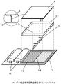
次に前記無線ガス検針システムに使用される無線アダプタにおける実装基板を説明する。図2は前記無線アダプタに内蔵されている基板実装形板状アンテナを持つ実装基板の外観構成図である。また図3はガスメータ1に前記板状アンテナを内蔵した無線アダプタ子機2を取り付けたときの外観構成図である。
【0026】
図2において8は板状アンテナの放射素子を形成する放射導体板、10は無線アダプタの制御回路を実装したプリント回路基板、11は片側の端部を放射導体板8に接続するとともにプリント回路基板10の放射導体板に対向した全面グランドに接続された短絡導体、12は前記プリント回路基板10の放射導体板側の全面グランドパターン(全面接地導体パターン)、14は高周波回路のアンテナ入出力端子に配線パターンを介して接続され、無線信号(高周波信号)を放射導体板8に給電する給電導体部、15は高周波回路をシールドするシールドケース、16はプリント回路基板10の表面に実装されるとともに無線アダプタの電源であるリチウム電池である。なお、全面グランドパターンは、放射導体板の特性に大きく関与する。例えば、全面グランドパターンの面積が広いほど、放射導体板から放射される電波の放射利得特性が良くなる可能性が高い。
【0027】
さらに図3に示すように前記プリント回路基板10に実装された無線機基板を樹脂製筐体に内蔵し無線アダプタ子機2として構成し、ガスメータ1の前面に取り付け接続して構成する。
【0028】
次に構成、動作及び作用について説明すると、図2における板状アンテナにおいて放射導体板8は端部に短絡導体11と給電導体部14を1枚の導体板により形成し、前記放射導体板8に対して短絡導体11及び給電導体部14は垂直に折り曲げて構成している。
【0029】
さらに短絡導体11と給電導体部14が一体として成型加工されている放射導体板8とプリント回路基板10の放射導体板8側片面全面グランド12とで板状アンテナを形成している。またプリント回路基板10上には無線機の電源であるリチウム電池16も実装されている構成である。そして前記プリント回路基板10上に形成された無線機を樹脂製筐体に内蔵し、無線アダプタ子機2または無線アダプタ親機3としてそれぞれガスメータ1または家屋壁面5などに取り付ける。
【0030】
また放射導体板8には利得を向上するため高導電率材料である銅を使用した構成である。
【0031】
また、プリント回路基板10は信号処理回路19と高周波回路18との間に導体からなるシールドシキリ17が取り付けられ、シールドシキリを樹脂コーティング外枠20の一部としてプリント回路基板の信号処理回路19と高周波回路18が樹脂コーティングされており、それを上部から覆うようにシールドケース15が接続されている。
【0032】
このような構成によれば、前記放射導体板8とプリント回路基板10の放射導体板8に対向した前記片面全面グランド12とで板状逆Fアンテナを構成することができることと、高周波回路とプリント回路基板上に樹脂コーティングをしようとする場合、高周波回路と信号処理回路の両方をそれぞれ枠取りし、それぞれ別枠で樹脂コーティングを実施していたものを1つの外枠で樹脂コーティングを実施することができるため、以上2つの理由により、構成部品を削減する事、さらに部品点数の削減と組み立て工数、調整工数の削減できる事、かつ高周波回路と信号処理回路の間の樹脂コーティング部未塗布部分がなくす事の3つが実現できる。
【0033】
なお、本実施例はガスメータの無線自動検針システムの無線アダプタを使用して説明したが、他の設備機器等の無線システムに使用される無線機でも良い。
【0034】
また、本実施例の構成は以下のどの実施例においても適用できると共に同様の効果がある。
【0035】
(実施例2)
図4は本発明の実施例2おける構成図である。
【0036】
図4において前記実施例と同一の構成要素については同一番号を付しているので説明は省略する。図4において、21は信号処理回路まで拡大したシールドケースである。
【0037】
このような構成によれば、高周波回路と信号処理回路の両方をシールドする場合にも1つのシールドケースで両方の部分をシールドすることができる。なお、このシールドケースは板状導体板の3辺を折り曲げて形成され、シールドケースの残りの折り曲げられていない1辺はシールドシキリの幅に合わせるという構成でも良い。
【0038】
(実施例3)
図5は本発明の実施例3における構成図である。
【0039】
図5において前記実施例と同一の構成要素については同一番号を付しているので説明は省略する。図5において、22は突起部を持つシールドシキリであり、23は孔部を持つシールドケースである。
【0040】
次に構成及び作用について説明すると、突起物を持つシールドシキリ22の突起部を、孔部を持つシールドケース23の孔部に挿入し、半田つけすることで、高周波回路のシールド効果を向上させることができる。
【0041】
(実施例4)
図6は本発明の実施例4における構成図である。
【0042】
図6において前記実施例と同一の構成要素については同一番号を付しているので説明は省略する。図6において、24はバネ性を有する突起部を持つシールドシキリである。
【0043】
次に構成及び作用について説明すると、バネ性を有する突起部を持つシールドシキリ24の突起部を、シールドケース21の内側に接触させることでシールドシキリ24とシールドケース21を電気的に導通させることで、半田つけすることなく、高周波回路のシールド効果を向上させることができる。
【0044】
なお、実施例では突起部で説明したがこれに限るものでなく、シールドシキリ24とシールドケースとを接触させる接触部であればよい。
【0045】
(実施例5)
図7は本発明の実施例5における構成図である。
【0046】
図7において前記実施例と同一の構成要素については同一番号を付しているので説明は省略する。図7において、25はシールドケース外枠部、26はシールドケースふた部である。
【0047】
次に構成及び作用について説明すると、シールドケース外枠部25をプリント回路基板10に接続し、そのあとこのシールドケース外枠部25を樹脂コーティングの外枠として樹脂をコーティングし、その後シールドケースふた部を上からかぶせ、シールドケース外枠部25とシールドケースふた部26を接触強度のみで保持させることができる。このため、樹脂コーティングの外枠を別に設ける必要もなく、シールドケース外枠部25の4面を上部の格子状部分でつなげているので、シールドケース外枠部25とシールドケースふた部26を半田つけすることなく接触強度だけで保持することができる。
【0048】
(実施例6)
図8は本発明の実施例6における構成図である。
【0049】
図8において前記実施例と同一の構成要素については同一番号を付しているので説明は省略する。図8において、27は板状導体板である。
【0050】
次に構成及び作用について説明すると、シールドシキリ17とシールドケース21の間に、板状導体板27がシールドシキリに取り付けられているので、実際に2重にシールドケースを設けることなく、低コストで2重シールド効果を実現することができる。
【0051】
なお、この板状導体板27は、基板と並行に取付る事を基本とするが、取付は、基板と並行でなくても良い。また、板状導体板27の大きさは、高周波回路か、信号処理部のどちらかを覆う形でもよいし、高周波回路と信号処理部の両方を覆う形でも良い。また、板状導体板27の大きさは限定しない。、
【0052】
【発明の効果】
以上説明したように本発明の無線回路は、高周波回路と信号処理回路との間にシールドシキリを設置しているため、高周波回路と信号処理回路のそれぞれを別々のコーティング枠で樹脂コーティングを実施していたものを1つの外枠で樹脂コーティングを実施することができ、かつ、高周波回路と信号処理回路の間の樹脂コーティング部未塗布部分がなくすることができる。
【図面の簡単な説明】
【図1】無線ガス自動検針システムのシステム構成図
【図2】本発明の実施例1における無線回路の構成図
【図3】本発明の実施例1における板状アンテナ内蔵無線アダプタのガスメータ取り付け構成図
【図4】本発明の実施例2における無線回路の構成図
【図5】本発明の実施例3における無線回路の構成図
【図6】本発明の実施例4における無線回路の構成図
【図7】本発明の実施例5における無線回路の構成図
【図8】本発明の実施例6における無線回路の構成図
【図9】従来の携帯無線機における無線回路の実装構成図
【符号の説明】
8 放射導体板
10 プリント回路基板
11 短絡導体
12 全面グランドパターン
14 給電導体部
15 シールドケース
16 リチウム電池
17 シールドシキリ
18 樹脂コーティングされた高周波回路
19 樹脂コーティングされた信号処理回路
20 樹脂コーティング外枠
21 信号処理回路まで拡大したシールドケース
22 突起部を持つシールドシキリ
23 孔部を持つシールドケース
24 バネ性を有する突起部を持つシールドシキリ
25 シールドケース外枠部
26 シールドケースふた部
27 板状導体板[0001]
BACKGROUND OF THE INVENTION
The present invention relates to a radio circuit of a radio used for remote control of an automatic gas meter reading system or equipment.
[0002]
[Prior art]
Conventionally, a monopole antenna, a loop antenna, or a plate-shaped inverted F antenna (hereinafter referred to as an inverted F antenna) is often used for a small wireless device. Among them, an inverted F antenna is small, thin, and has a relatively high gain, so that it is a mobile phone. It is often used as a built-in antenna for cordless telephones.
[0003]
FIG. 9 shows a conventional portable wireless device mounting structure. 9A is a front view, FIG. 9B is a side view, 40 is an inverted F antenna (unit), 41 is a radiating conductor plate that is a radiating element of the inverted F antenna, and 42 is a radiating conductor plate. Short-circuit conductor plate for grounding, 43 is a strip line for feeding a high-frequency signal, 44 is a feeding conductor plate for an inverted-F antenna connected to the strip line, and 45 is a high-frequency circuit on which a high-frequency circuit for transmitting and receiving radio signals is mounted. A printed circuit board on which a control circuit of the radio is mounted; 47 a shield case for shielding a high-frequency circuit or a printed circuit; 48 a ground conductor plate provided opposite to the radiation conductor plate; and 49 a ground The dielectric is loaded between the
[0004]
The inverted
[0005]
[Problems to be solved by the invention]
However, in the conventional configuration, when resin coating is to be performed on the high-frequency circuit and the printed circuit board, both the high-frequency circuit and the signal processing circuit are framed, and the resin coating is performed in a separate frame, respectively. The method of covering the shield case must be performed, and sufficient space must be secured for the frame of the resin coating, and the high-frequency circuit coating frame and the signal processing circuit between the high-frequency circuit and the signal processing circuit In order to install a shield case between the coating frame, it is necessary to have a resin-uncoated portion, and there is a problem that the resin coating cannot be performed on the wiring portion between the high-frequency circuit and the signal processing circuit.
[0006]
Also, if the high-frequency circuit is shielded alone and both the high-frequency circuit and the signal processing circuit are to be shielded, two shield cases are required: a high-frequency circuit shield case and a signal processing circuit shield case. There is also a problem that the cost becomes high considering the man-hours and material costs.
[0007]
In addition, when the shield case is divided into two parts, an outer frame part and a lid part, when the lid part is attached to the outer frame part by contact, strength cannot be obtained, and a connection method such as soldering the outer frame part and the lid part is required. .
[0008]
Further, in the above conventional example, when a shield case is placed on the high-frequency circuit unit and a short-circuit conductor is to be connected to the shield case, a separate conductor case is required, resulting in high cost.
[0009]
Further, when both the high-frequency circuit and the signal processing circuit are shielded and the short-circuit conductor of the inverted F antenna is to be connected, the high-frequency circuit shield case, the signal processing circuit shield case, and the two shield cases A short-circuit conductor has to be provided so as to cover it, and there has been a problem of high costs.
[0010]
SUMMARY OF THE INVENTION The present invention solves the above-mentioned problems, and in a large-sized component such as a battery or an RF unit, the mounting space and the dimension in the thickness direction are restricted. The resin coating is applied and both the high-frequency circuit and the signal processing circuit can be shielded at low cost. Even when the shield case is divided into two parts, the outer frame part and the lid part, the outer frame part and the lid part are connected by contact. It is possible to shield both the high-frequency circuit and the signal processing circuit and connect the short-circuit conductor of the inverted F antenna to achieve this effect at a low cost.
[0011]
[Means for Solving the Problems]
In order to solve the above-mentioned problems, the present invention provides a printed circuit board in which a shield consisting of a conductor is attached between a signal processing circuit and a high frequency circuit, and this shield is used as a part of the outer frame of the resin coating. Are connected between the signal processing circuit and the high-frequency circuit.
[0012]
Further, the shield case is formed by bending three sides of the plate-like conductor plate, and the other one side of the plate-like conductor plate that is not bent is adjusted to the width of the shield gap, thereby making this shield case a printed circuit. When connecting to a substrate, both the signal processing circuit and the high-frequency circuit can be shielded.
[0013]
The shield case is composed of two parts, an outer frame portion and a lid portion, and the outer frame portion has a surface facing the radiation conductor plate connected by a conductor such as a lattice.
[0014]
The printed circuit board has a shield gap made of a conductor between the signal processing circuit and the high-frequency circuit, and a plate-like conductor plate attached to the shield gap between the shield gap and the shield case.
[0015]
DETAILED DESCRIPTION OF THE INVENTION
The present invention provides a printed circuit board having a signal processing circuit and a high-frequency circuit wiring pattern on one side and a grounding conductor pattern on the other side, a radiation conductor plate facing the surface of the grounding conductor pattern, and the radiation A short-circuit conductor having one end connected to a conductor plate, a power supply conductor portion that supplies a high-frequency signal to the radiation conductor plate, and a shield case that shields a high-frequency circuit, and the printed circuit board includes the signal processing circuit and the high-frequency signal A shield circuit made of a conductor is attached between the circuit and the signal processing circuit of the printed circuit board and the high-frequency circuit are resin-coated using the shield cable as a part of the outer frame of the resin coating. Formed.
[0016]
As a result, when resin coating is to be applied to the high-frequency circuit and the printed circuit board, both the high-frequency circuit and the signal processing circuit are framed, and the ones that have been resin-coated in separate frames are combined into one outer frame. Since the resin coating is applied, the number of components can be reduced, the number of parts can be reduced, the number of assembly and adjustment processes can be reduced, and the uncoated part of the resin coating between the high-frequency circuit and the signal processing circuit can be eliminated. be able to.
[0017]
In the present invention, a shield gap is attached between the signal processing circuit and the high-frequency circuit, and when the shield case is connected to the printed circuit board, both the signal processing circuit and the high-frequency circuit are shielded. Thus, both the signal processing circuit and the high frequency circuit can be shielded.
[0018]
Further, the present invention improves the shielding effect of the high-frequency circuit by having the projection in the shield and the hole in the short-circuit conductor plate, and the short-circuit conductor plate is inserted and connected to the projection in the hole in the hole. be able to.
[0019]
Further, according to the present invention, the shield shim has a contact part having a spring property, and the connection between the short-circuit conductor plate and the shield shim is electrically contacted by the contact part having the spring property of the shield shim so that the shield property of the high frequency circuit is obtained. Can be improved without soldering.
[0020]
According to the present invention, the shield case includes an outer frame portion and a lid portion, and the outer frame portion is connected to a surface facing the radiation conductor plate, so that the outer frame of the shield and the outer surface of the resin coating are provided. The frame can also be used, and sufficient lid mounting strength can be provided by contact alone without soldering the outer frame portion and the lid portion.
[0021]
Further, the present invention attaches a shield made of a conductor between the signal processing circuit of the printed circuit board and the high frequency circuit, and further attaches a plate-like conductor plate between the shield and the shield case to the shield. Even when both the circuit and the signal processing circuit are shielded and the shorted conductor of the inverted F antenna is to be connected, this effect can be realized at low cost.
[0022]
【Example】
Example 1
[0023]
In FIG. 1, 1 is a gas meter that integrates and measures the gas usage of a consumer, 2 is a wireless adapter slave connected to the gas meter and communicates wirelessly, and 3 is a wireless adapter parent that communicates wirelessly with the wireless adapter slave. 4 is a T-NCU (Terminal-Network Control Unit), to which a wireless adapter base unit is connected and has a line control function, 5 is a wall surface of the house where the T-
[0024]
Next, the operation will be described. The meter reading center 7 of the gas supplier transmits a gas metering request to the
The wireless
[0025]
Next, a mounting board in a wireless adapter used in the wireless gas meter reading system will be described. FIG. 2 is an external configuration diagram of a mounting board having a board-mounted plate antenna built in the wireless adapter. FIG. 3 is an external configuration diagram when the wireless
[0026]
In FIG. 2, 8 is a radiating conductor plate forming a radiating element of a plate antenna, 10 is a printed circuit board on which a control circuit of the wireless adapter is mounted, and 11 is a printed circuit board having one end connected to the radiating
[0027]
Further, as shown in FIG. 3, the wireless device board mounted on the printed
[0028]
Next, the configuration, operation, and action will be described. In the plate-like antenna in FIG. 2, the
[0029]
Furthermore, a plate-like antenna is formed by the
[0030]
The radiating
[0031]
The printed
[0032]
According to such a configuration, a plate-like inverted F antenna can be configured by the
[0033]
In addition, although the present Example demonstrated using the radio | wireless adapter of the radio | wireless automatic meter-reading system of a gas meter, the radio | wireless machine used for radio | wireless systems, such as another installation apparatus, may be used.
[0034]
The configuration of the present embodiment can be applied to any of the following embodiments and has the same effect.
[0035]
(Example 2)
FIG. 4 is a configuration diagram in
[0036]
In FIG. 4, the same components as those in the above embodiment are given the same numbers, and the description thereof is omitted. In FIG. 4,
[0037]
According to such a configuration, even when both the high-frequency circuit and the signal processing circuit are shielded, both portions can be shielded by one shield case. The shield case may be formed by bending three sides of the plate-like conductor plate, and the remaining one side of the shield case not being bent may be adjusted to the width of the shield.
[0038]
(Example 3)
FIG. 5 is a configuration diagram in
[0039]
In FIG. 5, the same components as those in the above embodiment are given the same numbers, and the description thereof is omitted. In FIG. 5,
[0040]
Next, the configuration and operation will be described. The projecting portion of the
[0041]
Example 4
FIG. 6 is a configuration diagram in
[0042]
In FIG. 6, the same components as those in the above embodiment are given the same numbers, and the description thereof is omitted. In FIG. 6,
[0043]
Next, the configuration and operation will be described. By bringing the projection of the
[0044]
In addition, although demonstrated in the Example about the protrusion part, it is not restricted to this, What is necessary is just a contact part which contacts the
[0045]
(Example 5)
FIG. 7 is a configuration diagram in Embodiment 5 of the present invention.
[0046]
In FIG. 7, the same components as those in the above embodiment are given the same numbers, and the description thereof is omitted. In FIG. 7, 25 is a shield case outer frame part, and 26 is a shield case cover part.
[0047]
Next, the structure and operation will be described. The shield case
[0048]
(Example 6)
FIG. 8 is a configuration diagram in Embodiment 6 of the present invention.
[0049]
In FIG. 8, the same components as those in the above embodiment are given the same numbers, and the description thereof is omitted. In FIG. 8,
[0050]
Next, the configuration and operation will be described. Since the plate-
[0051]
The plate-
[0052]
【The invention's effect】
As described above, since the wireless circuit of the present invention has a shield gap between the high frequency circuit and the signal processing circuit, each of the high frequency circuit and the signal processing circuit is coated with a resin in a separate coating frame. It is possible to carry out resin coating with a single outer frame, and to eliminate the uncoated portion of the resin coating portion between the high frequency circuit and the signal processing circuit.
[Brief description of the drawings]
FIG. 1 is a system configuration diagram of a wireless gas automatic meter reading system. FIG. 2 is a configuration diagram of a wireless circuit in
DESCRIPTION OF
Claims (3)
前記接地導体パターンの面に対向させた放射導体板と、
前記放射導体板に一方の端部を接続した短絡導体と、
前記放射導体板に高周波信号を供給する給電導体部と、
前記信号処理回路と前記高周波回路との間に、前記信号処理回路と前記高周波回路とを周囲から取り囲むようにして形成された樹脂コーティング外枠を横切るようにして設けられた導体からなるシールドシキリと、
前記樹脂コーティング外枠と前記シールドシキリによって囲まれた箇所に形成して前記信号処理回路と前記高周波回路を覆う樹脂コーティングと、
前記高周波回路の上方および周囲三方をシールドするシールドケースを備え、
前記シールドケースと前記シールドシキリとを組み合わせて配置することで前記高周波回路を上面と周囲四方から取り囲む
ことを特徴とする無線回路。A printed circuit board having a signal processing circuit and a high-frequency circuit wiring pattern on one side, and a grounding conductor pattern on the other side;
A radiation conductor plate facing the surface of the ground conductor pattern;
A short-circuit conductor having one end connected to the radiation conductor plate;
A feeding conductor for supplying a high-frequency signal to the radiation conductor plate ;
Between the signal processing circuit and the high frequency circuit, a shield gap made of a conductor provided so as to cross a resin coating outer frame formed so as to surround the signal processing circuit and the high frequency circuit from the surroundings ; ,
A resin coating that covers the signal processing circuit and the high-frequency circuit by being formed at a location surrounded by the resin coating outer frame and the shield gap;
Comprising a shield case for shielding the upper and three sides of the high-frequency circuit,
A radio circuit characterized by surrounding the high-frequency circuit from the upper surface and surrounding four sides by arranging the shield case and shield shield in combination .
前記シールドケースはこの孔に前記シールドシキリの突起部を差し込んで接続することを特徴とする請求項2記載の無線回路。 It includes a protrusion on the shield sheet Kiri, comprising a hole in the shield case,
3. The radio circuit according to claim 2, wherein the shield case is connected by inserting a projection portion of the shield gap into the hole.
Priority Applications (1)
| Application Number | Priority Date | Filing Date | Title |
|---|---|---|---|
| JP2001210448A JP4524964B2 (en) | 2001-07-11 | 2001-07-11 | Wireless circuit |
Applications Claiming Priority (1)
| Application Number | Priority Date | Filing Date | Title |
|---|---|---|---|
| JP2001210448A JP4524964B2 (en) | 2001-07-11 | 2001-07-11 | Wireless circuit |
Publications (2)
| Publication Number | Publication Date |
|---|---|
| JP2003032138A JP2003032138A (en) | 2003-01-31 |
| JP4524964B2 true JP4524964B2 (en) | 2010-08-18 |
Family
ID=19045921
Family Applications (1)
| Application Number | Title | Priority Date | Filing Date |
|---|---|---|---|
| JP2001210448A Expired - Fee Related JP4524964B2 (en) | 2001-07-11 | 2001-07-11 | Wireless circuit |
Country Status (1)
| Country | Link |
|---|---|
| JP (1) | JP4524964B2 (en) |
Families Citing this family (3)
| Publication number | Priority date | Publication date | Assignee | Title |
|---|---|---|---|---|
| JP4716169B2 (en) * | 2005-04-22 | 2011-07-06 | 横河電機株式会社 | License management device |
| JP4647407B2 (en) * | 2005-06-17 | 2011-03-09 | 大井電気株式会社 | Waterproof case |
| US8694060B2 (en) * | 2008-06-17 | 2014-04-08 | Rosemount Inc. | Form factor and electromagnetic interference protection for process device wireless adapters |
Citations (7)
| Publication number | Priority date | Publication date | Assignee | Title |
|---|---|---|---|---|
| JPS59151497U (en) * | 1983-03-29 | 1984-10-11 | 日本電気ホームエレクトロニクス株式会社 | Shield partition plate |
| JPS60103894U (en) * | 1983-12-22 | 1985-07-15 | 日本ビクター株式会社 | Electromagnetic shield mechanism |
| JPH04287409A (en) * | 1991-03-15 | 1992-10-13 | Nippon Telegr & Teleph Corp <Ntt> | Small sized radio equipment |
| JPH08111609A (en) * | 1994-10-11 | 1996-04-30 | Murata Mfg Co Ltd | Antenna system |
| JPH11307968A (en) * | 1998-04-20 | 1999-11-05 | Matsushita Electric Ind Co Ltd | Heat-dissipating structure of electronic controller |
| JP2000165137A (en) * | 1998-11-24 | 2000-06-16 | Matsushita Electric Ind Co Ltd | Board mounted planar antenna |
| JP2000294950A (en) * | 1999-04-09 | 2000-10-20 | Matsushita Electric Ind Co Ltd | High-frequency apparatus |
-
2001
- 2001-07-11 JP JP2001210448A patent/JP4524964B2/en not_active Expired - Fee Related
Patent Citations (7)
| Publication number | Priority date | Publication date | Assignee | Title |
|---|---|---|---|---|
| JPS59151497U (en) * | 1983-03-29 | 1984-10-11 | 日本電気ホームエレクトロニクス株式会社 | Shield partition plate |
| JPS60103894U (en) * | 1983-12-22 | 1985-07-15 | 日本ビクター株式会社 | Electromagnetic shield mechanism |
| JPH04287409A (en) * | 1991-03-15 | 1992-10-13 | Nippon Telegr & Teleph Corp <Ntt> | Small sized radio equipment |
| JPH08111609A (en) * | 1994-10-11 | 1996-04-30 | Murata Mfg Co Ltd | Antenna system |
| JPH11307968A (en) * | 1998-04-20 | 1999-11-05 | Matsushita Electric Ind Co Ltd | Heat-dissipating structure of electronic controller |
| JP2000165137A (en) * | 1998-11-24 | 2000-06-16 | Matsushita Electric Ind Co Ltd | Board mounted planar antenna |
| JP2000294950A (en) * | 1999-04-09 | 2000-10-20 | Matsushita Electric Ind Co Ltd | High-frequency apparatus |
Also Published As
| Publication number | Publication date |
|---|---|
| JP2003032138A (en) | 2003-01-31 |
Similar Documents
| Publication | Publication Date | Title |
|---|---|---|
| JP4306970B2 (en) | Radiant enclosure | |
| EP1102347B1 (en) | Integrated antenna ground plate and EMC shield structure | |
| JP3664792B2 (en) | Portable radio | |
| CN102870276B (en) | Cavity-backed slot antenna with near-field-coupled parasitic slot | |
| US6285327B1 (en) | Parasitic element for a substrate antenna | |
| EP2458676B1 (en) | Antenna apparatus for portable terminal | |
| JP2002064601A (en) | Mobile telephone device and its built-in antenna | |
| EP1154517B1 (en) | Radio frequency antenna | |
| US9601831B2 (en) | Radio device | |
| CN101385193A (en) | Multipart case wireless communications device with multiple groundplane connectors | |
| JP2003069442A (en) | Radio module and radio communication apparatus with the radio module | |
| US20140240195A1 (en) | Electronic Device With Diverse Antenna Array Having Soldered Connections | |
| JP4435978B2 (en) | Substrate antenna incorporating elements that prevent energy coupling between antenna and conductor | |
| JPH10313212A (en) | Board mount plate antenna | |
| JP4524964B2 (en) | Wireless circuit | |
| KR100738265B1 (en) | Substrate antenna | |
| KR101305283B1 (en) | Portable terminal having antenna apparatus | |
| JP2006093998A (en) | Mobile communication apparatus | |
| CN111864346A (en) | Bluetooth antenna structure and bluetooth wearing equipment | |
| TWI225336B (en) | Module for transmitting and/or receiving radio data | |
| CN219801246U (en) | Electronic equipment | |
| JP2005020766A (en) | Mobile radio equipment | |
| CN218827793U (en) | Antenna structure for mobile device and mobile device | |
| JP2000165137A (en) | Board mounted planar antenna | |
| JP3960191B2 (en) | ANTENNA AND ELECTRIC DEVICE HAVING THE SAME |
Legal Events
| Date | Code | Title | Description |
|---|---|---|---|
| A621 | Written request for application examination |
Free format text: JAPANESE INTERMEDIATE CODE: A621 Effective date: 20080207 |
|
| RD01 | Notification of change of attorney |
Free format text: JAPANESE INTERMEDIATE CODE: A7421 Effective date: 20080312 |
|
| RD01 | Notification of change of attorney |
Free format text: JAPANESE INTERMEDIATE CODE: A7421 Effective date: 20091119 |
|
| A977 | Report on retrieval |
Free format text: JAPANESE INTERMEDIATE CODE: A971007 Effective date: 20091211 |
|
| A131 | Notification of reasons for refusal |
Free format text: JAPANESE INTERMEDIATE CODE: A131 Effective date: 20091222 |
|
| A521 | Written amendment |
Free format text: JAPANESE INTERMEDIATE CODE: A523 Effective date: 20100217 |
|
| TRDD | Decision of grant or rejection written | ||
| A01 | Written decision to grant a patent or to grant a registration (utility model) |
Free format text: JAPANESE INTERMEDIATE CODE: A01 Effective date: 20100511 |
|
| A01 | Written decision to grant a patent or to grant a registration (utility model) |
Free format text: JAPANESE INTERMEDIATE CODE: A01 |
|
| A61 | First payment of annual fees (during grant procedure) |
Free format text: JAPANESE INTERMEDIATE CODE: A61 Effective date: 20100524 |
|
| FPAY | Renewal fee payment (event date is renewal date of database) |
Free format text: PAYMENT UNTIL: 20130611 Year of fee payment: 3 |
|
| FPAY | Renewal fee payment (event date is renewal date of database) |
Free format text: PAYMENT UNTIL: 20130611 Year of fee payment: 3 |
|
| R250 | Receipt of annual fees |
Free format text: JAPANESE INTERMEDIATE CODE: R250 |
|
| LAPS | Cancellation because of no payment of annual fees |