JP3664792B2 - Portable radio - Google Patents
Portable radio Download PDFInfo
- Publication number
- JP3664792B2 JP3664792B2 JP01162296A JP1162296A JP3664792B2 JP 3664792 B2 JP3664792 B2 JP 3664792B2 JP 01162296 A JP01162296 A JP 01162296A JP 1162296 A JP1162296 A JP 1162296A JP 3664792 B2 JP3664792 B2 JP 3664792B2
- Authority
- JP
- Japan
- Prior art keywords
- antenna
- built
- shield
- antenna element
- shield chassis
- Prior art date
- Legal status (The legal status is an assumption and is not a legal conclusion. Google has not performed a legal analysis and makes no representation as to the accuracy of the status listed.)
- Expired - Fee Related
Links
Images


Classifications
-
- H—ELECTRICITY
- H01—ELECTRIC ELEMENTS
- H01Q—ANTENNAS, i.e. RADIO AERIALS
- H01Q1/00—Details of, or arrangements associated with, antennas
- H01Q1/12—Supports; Mounting means
- H01Q1/22—Supports; Mounting means by structural association with other equipment or articles
- H01Q1/24—Supports; Mounting means by structural association with other equipment or articles with receiving set
- H01Q1/241—Supports; Mounting means by structural association with other equipment or articles with receiving set used in mobile communications, e.g. GSM
- H01Q1/242—Supports; Mounting means by structural association with other equipment or articles with receiving set used in mobile communications, e.g. GSM specially adapted for hand-held use
- H01Q1/243—Supports; Mounting means by structural association with other equipment or articles with receiving set used in mobile communications, e.g. GSM specially adapted for hand-held use with built-in antennas
-
- H—ELECTRICITY
- H01—ELECTRIC ELEMENTS
- H01Q—ANTENNAS, i.e. RADIO AERIALS
- H01Q1/00—Details of, or arrangements associated with, antennas
- H01Q1/52—Means for reducing coupling between antennas; Means for reducing coupling between an antenna and another structure
- H01Q1/526—Electromagnetic shields
-
- H—ELECTRICITY
- H01—ELECTRIC ELEMENTS
- H01Q—ANTENNAS, i.e. RADIO AERIALS
- H01Q9/00—Electrically-short antennas having dimensions not more than twice the operating wavelength and consisting of conductive active radiating elements
- H01Q9/04—Resonant antennas
- H01Q9/0407—Substantially flat resonant element parallel to ground plane, e.g. patch antenna
- H01Q9/0421—Substantially flat resonant element parallel to ground plane, e.g. patch antenna with a shorting wall or a shorting pin at one end of the element
Description
【0001】
【発明の属する技術分野】
本発明は携帯電話機、コードレス電話機等の携帯無線機の内蔵アンテナ取付構造及びシールド構造に関する。
【0002】
近年、通信需要の拡大に伴って、携帯電話機等の携帯無線機が広く実用に供されている。携帯無線機は、通常携帯時における受信機能を確保するために、装置筐体内にアンテナを内蔵している。
【0003】
この内蔵アンテナは、共振周波数、帯域幅、利得等について所望の電気的特性が得られていることを前提に、小型化及び軽量化に適し、且つ組み立て性に優れたものであることが要求される。
【0004】
また、携帯無線機は、小型軽量化の要請により薄肉化されたケースの使用が必要であり、ケース内部には高密度実装された多数の電子部品が収容される。このような携帯無線機には、準マイクロ波帯と呼ばれる800〜900MHz前後の高周波帯域が利用されるため、ケースの軽量化を図りながらケース内部の電磁シールドを強化して、電磁干渉による様々な障害を防止する必要がある。
【0005】
【従来の技術】
従来の携帯電話機の内蔵アンテナとしては板状逆F形アンテナが知られている。この逆F形アンテナをプリント配線板に直接実装し、待機時における受信機能を確保している。
【0006】
また、携帯電話機の従来のシールド構造は、プリント配線板のグランドパターンにU字形ばねを半田付けし、リブを有する樹脂モールドケース内面にメッキ、静電塗装、アルミニウムの蒸着等により金属皮膜を形成し、U字形ばねをリブにかみ合わせてモールドケース内面に接触させていた。
【0007】
【発明が解決しようとする課題】
しかし、上述したような従来の内蔵アンテナ取付構造では、プリント配線板上に内蔵アンテナを実装していたため、プリント配線板の部品実装領域を確保するのが容易ではなく、携帯無線機の小型化・薄型化が困難であった。
【0008】
従来のシールド構造では、プリント配線板にU字形ばねを半田付けしていたため、ばねの取付工数が多くかかるという問題があると共に、高密度実装化には対応できないという問題があった。
【0009】
よって本発明の目的は、部品の高密度実装化に適した携帯無線機の内蔵アンテナ取付構造及びシールド構造を提供することである。
【0010】
【課題を解決するための手段】
本発明によると、携帯無線機の内蔵アンテナ取付構造であって、アンテナ搭載面を除いてその表面及び裏面が導電処理された樹脂モールド製シールドシャーシと;前記シールドシャーシ上に搭載された、送受信回路を有するプリント配線板と;前記シールドシャーシ上のアンテナ搭載面に取り付けられた金属板からなる内蔵アンテナと;前記送受信回路と前記内蔵アンテナとを接続する同軸ケーブルとを具備し;前記内蔵アンテナは平板状のアンテナエレメントと、該アンテナエレメントを前記シールドシャーシに短絡するばね性を有する短絡板を有しており、該短絡板と前記アンテナエレメントで前記シールドシャーシのエッジ部を挟み込むことにより前記内蔵アンテナは前記シールドシャーシに取り付けられ;前記同軸ケーブルの芯線が前記短絡板から所定距離離間して前記アンテナエレメントに半田付けされていることを特徴とする携帯無線機の内蔵アンテナ取付構造が提供される。
【0011】
内蔵アンテナをシールドシャーシに実装したため、プリント配線板の部品実装領域を十分に確保することができ、携帯無線機の小型化、薄型化及びコストダウンを図ることができる。
【0014】
【発明の実施の形態】
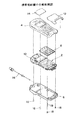
図1を参照すると、本発明の内蔵アンテナ取付構造及びシールド構造を有する携帯電話機の分解斜視図が示されている。符号2はプリント配線板アセンブリであり、液晶ディスプレイ10を有している。
【0015】
プリント配線板アセンブリ2上にキーパッド8が搭載され、フロントケース4及びリアケース6でプリント配線板アセンブリ2をサンドイッチして、ネジ18を締めつけることによりプリント配線板アセンブリ2、フロントケース4及びリアケース6が一体的に組み立てられる。
【0016】
リアケース6には通話時に引き出して使用されるロッドアンテナ16が引き出し及び収納可能に取り付けられている。フロントケース4にはカバー12及び表示窓14が取り付けられる。
【0017】
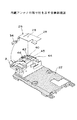
図2を参照すると、プリント配線板アセンブリ2を背面側から見た分解斜視図が示されている。プリント配線板アセンブリ2は、多層プリント配線板20をシールドシャーシ22及びフロントシールド24でサンドイッチして構成する。
【0018】
シールドシャーシ22は樹脂モールド製であり、アンテナ搭載面40及びバイブレータ搭載面41を除いてその表面及び裏面が斜線で示す如く導電処理されている。バイブレータ25がバイブレータ搭載面41に搭載される。
【0019】
同様に、フロントシールド24も樹脂モールド製であり、その全表面が導電処理されている。具体的には、この導電処理は無電解メッキで行われ、まず下地の銅をメッキした後、銅メッキの上にニッケルメッキが施される。
【0020】
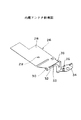
符号26は逆F形の内蔵アンテナを示しており、例えば銅等の金属板を折り曲げ加工及び打ち抜き加工して形成される。図4に最もよく示されているように、内蔵アンテナ26は平板状のアンテナエレメント28と、アンテナエレメント28に対して概略直角に折り曲げられた連結部32と、アンテナエレメント28に平行なグランドエレメント34と、短絡板(ショートピン)30を含んでいる。
【0021】
符号38は同軸ケーブルの外部導体半田付け固定部であり、グランドエレメント34に導通している。アンテナエレメント28と連結部32との間にはスリット33が形成されている。アンテナエレメント28は位置決め用の穴29を有している。グランドエレメント34は、グランドエレメント34をシールドシャーシ22に固定する係合突起36を有している。
【0022】
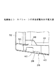
図3を参照すると、シールドシャーシ22はアンテナ搭載面40を有している。アンテナ搭載面40はメッキ処理されていずに絶縁性であり、格子状のリブ45と2つの位置決め用リブ44,46を含んでいる。
【0023】
格子状リブ45の中央にはアンテナエレメント28に形成された穴29に挿入される位置決め用の突起42が設けられている。
アンテナ26をシールドシャーシ22のアンテナ搭載面40に搭載するには、アンテナエレメント28の両サイドエッジを位置決め用リブ44,46の内側に合わせ、更にアンテナエレメント28の穴29中に位置決め用突起42を挿入することにより、アンテナ26をアンテナ搭載面40に位置決めして搭載する。
【0024】
この時、図5に示すようにばね性を有する短絡板30とアンテナエレメント28でシールドシャーシ22のエッジ部を挟み込む。短絡板40はシールドシャーシ22に形成されたニッケルメッキ膜48に圧接される。
【0025】
更に、図6に示すようにグランドエレメント34に形成された係合突起36がシールドシャーシ22に形成された穴23に係合し、グランドエレメント34がシールドシャーシ22に固定される。
【0026】
好ましくは、アンテナエレメント28のアンテナ搭載面40への固定を確実にするために、両面粘着テープを使用してアンテナエレメント28をアンテナ搭載面40に接着する。
【0027】
図7に示すように、同軸ケーブル50の一端にはプリント配線板20に搭載された送受信回路に接続される同軸コネクタ52が接続されている。同軸ケーブル50の他端部では外被が除去されて外部導体56がアンテナ26の外部導体固定部38に半田付けされている。
【0028】
アンテナエレメント28には同軸ケーブルの配線方向と概略平行なブリッジ57が形成されており、このブリッジ54の下を絶縁皮膜54を被った芯線(内部導体)58をくぐらせ、給電点60で芯線58がアンテナエレメント28に半田付けされている。
【0029】
即ち、図8(A)に示すように芯線58をブリッジ54の下をくぐらせ、図8(B)に示すように芯線58の直径よりもわずかばかり広い間隔を有する一対の突起62の間に芯線58を通すことにより、芯線を位置決めし、芯線58をアンテナエレメント28に半田付けする。
【0030】
これにより、アンテナ26の給電点60を短絡板30からあらかじめ計算した所定距離離間して設けることができる。同軸ケーブル50の配線方向と概略平行方向に伸長するブリッジ54の下を芯線58をくぐらせてから芯線をアンテナエレメント28に半田付けしているため、給電点60での芯線58への負荷を少なくすることができる。
【0031】
更に、内蔵アンテナ26(逆F型アンテナ)のグランド面はプリント配線板20をシールドするシールドシャーシ22の導電性裏面と共通化することができる。
【0032】
従って、アンテナエレメント28をシールドメッキされていないシャーシのアンテナ搭載面40に搭載することを可能とし、且つプリント配線板20にアンテナ搭載領域を設ける必要がない。よって、プリント配線板を小型化でき、携帯電話機自身の小型化を達成できる。
【0033】
図9を参照すると、本発明の他の実施形態の内蔵アンテナ取付構造が示されている。本実施形態では、アンテナ搭載面40の格子状リブ45で画成されたポケット47中に誘電体64を挿入する。
【0034】
これにより、内蔵アンテナ26のアンテナ特性を向上することができ、より小さな内蔵アンテナでも十分な性能を発揮することができる。本実施形態の他の構成は、上述した実施形態と同様であるのでその説明を省略する。
【0035】
次に図10を参照して、本実施形態にかかる携帯電話機の送信信号の流れを概略的に説明する。送信信号の流れに沿って、電圧制御発振器(高周波発振器)66、アイソレータ70及び高周波フィルタ72をプリント配線板20上に高密度実装するためには、電圧制御発振器66の近くにアイソレータ70及び高周波フィルタ72を実装しなければならない。
【0036】
プリント配線板20の裏面に実装されたミキサー64で主信号Sと電圧制御発振器66からのキャリアがミキシングされ、プリアンプ68で増幅される。このプリアンプ68で増幅された信号がアイソレータ70及び高周波フィルタ72を介してロッドアンテナ16に接続されたコネクタ74に供給される。
【0037】
このように、電圧制御発振器66の近くにアイソレータ70及び高周波フィルタ72を実装しているため、プリアンプ68で増幅された信号が電圧制御発振器66に回り込み変調精度を劣化させていた。これを防止するために、電圧制御発振器66とアイソレータ70及び高周波フィルタ72との間を電磁シールドする必要がある。
【0038】
図11を参照すると、本発明シールド構造の第1実施形態分解斜視図が示されている。プリント配線板20は内部にグランド層を有する多層プリント配線板であり、その表面にはこのグランド層に接続された一対の(1つのみ図示)パッド92が露出している。
【0039】
プリント配線板20上には電圧制御発振器66に隣接してアイソレータ70及び高周波フィルタ72が実装されている。符号76は受信用の電子部品を示している。
【0040】
符号80はリン青銅から形成された金属シールド板であり、アイソレータ70及び高周波フィルタ72の配置に応じた屈曲した形状をしている。金属シールド板80はプリント配線板20に対して垂直に実装される本体部分82と、この本体部分82に対して概略直角に折り曲げられた複数の屈曲部84を有している。各屈曲部84には舌片86が切り起こしにより形成されている。各舌片86はばね性を有しており、弾性変形可能である。
【0041】
金属シールド板80の本体部分82から下方に突出して一対の位置決め用突起88が設けられており、更に半田付け用の一対の足90が横方向に突出している。
【0042】
プリント配線板20にはこの位置決め用の突起88が挿入される一対の(1つのみ図示)位置決め穴89が形成されている。
しかして、金属シールド板80の一対の突起88をプリント配線板20の位置決め穴89に挿入することにより、金属シールド板80を位置決めしてプリント配線板20に実装する。そして、金属シールド板80の一対の足90をプリント配線板20のパッド92に半田付けする。
【0043】
プリント配線板20の上からその表面がニッケルメッキされたシールドシャーシ22をかぶせ、両者をねじ止めすることにより金属シールド板80の舌片86がシールドシャーシ22に圧接され、電圧制御発振器66とアイソレータ70及び高周波フィルタ72との間を効果的に電磁シールドすることができる。
【0044】
本実施形態のシールド構造は、金属シールド板80の本体部分82を立ててプリント配線板20に実装し、本体部分82に対して概略90°折り曲げられた舌片86をシールドシャーシ22に圧接しているので、シールド板80の設置にあまりスペースを取ることなく、高密度実装された電子部品間を効果的に電磁シールドすることができる。
【0045】
図12を参照すると、本発明シールド構造の第2実施形態分解斜視図が示されている。本実施形態の金属シールド板80′は金属シールド板を位置決めするための位置決め構造が上述した第1実施形態と相違する。本実施形態の他の構成は上述した第1実施形態と同様であるので、その説明を省略する。
【0046】
即ち、本実施形態の金属シールド板80′は、図13に最も良く示されるように受信用電子部品76にかぶせられる一対の位置決め用の当て94と、図14に最もよく示されるように、金属シールド板80′がアイソレータ70と受信用電子部品76との間に挿入されたとき、アイソレータ70に当接する位置決め用の切り起こし96とを有している。
【0047】
このように、一対の当て94が電子部品76にかぶせられるため、金属シールド板80′を位置決めすることができ、更に切り起こし96がアイソレータ70に当接するため、金属シールド板80′をがたつくことなくプリント配線板20上に実装することができる。金属シールド板80′の足90はプリント配線板20のパッド92に半田付けされる。
【0048】
本実施形態でも図11に示すようにシールドシャーシ22がプリント配線板20に上方からかぶせられるため、金属シールド板80′の舌片86がシールドシャーシ22に圧接される。
【0049】
また、上述した第1実施形態と同様に、高密度実装された電子部品間を効果的に電磁シールドすることができる。更に本実施形態では、プリント配線板20に位置決め用の穴を設ける必要がないので、多層プリント配線板のパターニングの自由度が大きくなる。
【0050】
上述した第2実施形態では、位置決め用の当て94を受信用電子部品76にかぶせているが、本発明はこれに限定されるものではなく、金属シールド板80′の形状を変えて当て94をアイソレータ70又は高周波フィルタ72に当接させるようにしてもよい。
【0051】
更に、位置決め用の当て94は必ずしも一対設ける必要はなく、1つのみ設けていずれかの電子部品70,72,76の一面に当てを押しつけることにより、金属シールド板80′を位置決めするようにしてもよい。
【0052】
【発明の効果】
本発明の内蔵アンテナ取付構造によれば、内蔵アンテナをプリント配線板ではなくシールドシャーシに実装するようにしたので、内蔵アンテナがプリント配線板の実装領域を妨げることなく、プリント配線板の高密度実装が可能となる。
【図面の簡単な説明】
【図1】本発明の内蔵アンテナ取付構造及びシールド構造を有する携帯電話機の分解斜視図である。
【図2】プリント配線板アセンブリの分解斜視図である。
【図3】内蔵アンテナのシールドシャーシへの取り付けを示す分解斜視図である。
【図4】内蔵アンテナ斜視図である。
【図5】短絡板とシールドシャーシの係合状態を示す拡大図である。
【図6】図3のA部分拡大断面図である。
【図7】内蔵アンテナの背面図である。
【図8】同軸ケーブル芯線の固定方法説明図である。
【図9】内蔵アンテナの取付構造の他の実施形態分解斜視図である。
【図10】送信信号の流れを示す概略図である。
【図11】本発明シールド構造の第1実施形態分解斜視図である。
【図12】本発明シールド構造の第2実施形態分解斜視図である。
【図13】図12のA方向矢視図である。
【図14】図12のB方向矢視図である。
【符号の説明】
2 プリント配線板アセンブリ
4 フロントケース
6 リアケース
20 プリント配線板
22 シールドシャーシ
26 内蔵アンテナ
28 アンテナエレメント
30 短絡板
34 グランドエレメント
40 アンテナ搭載面
66 電圧制御発振器
70 アイソレータ
72 高周波フィルタ
80,80′ 金属シールド板
86 舌片[0001]
BACKGROUND OF THE INVENTION
The present invention relates to a built-in antenna mounting structure and a shield structure of a portable wireless device such as a mobile phone and a cordless phone.
[0002]
In recent years, with the expansion of communication demand, portable wireless devices such as mobile phones have been widely put into practical use. In order to ensure a reception function when the portable wireless device is normally carried, an antenna is built in the device casing.
[0003]
This built-in antenna is required to be suitable for downsizing and weight reduction and to be excellent in assembling, on the premise that desired electrical characteristics such as resonance frequency, bandwidth and gain are obtained. The
[0004]
In addition, the portable wireless device requires the use of a thinned case in response to a demand for a reduction in size and weight, and a large number of electronic components mounted at high density are accommodated inside the case. Since such a portable wireless device uses a high frequency band of about 800 to 900 MHz called a quasi-microwave band, the electromagnetic shield inside the case is strengthened while reducing the weight of the case, and various types of electromagnetic interference are caused. It is necessary to prevent obstacles.
[0005]
[Prior art]
As a built-in antenna of a conventional mobile phone, a plate-like inverted F-shaped antenna is known. This inverted-F antenna is directly mounted on a printed wiring board to ensure a reception function during standby.
[0006]
In addition, the conventional shield structure of a cellular phone is such that a U-shaped spring is soldered to the ground pattern of a printed wiring board, and a metal film is formed on the inner surface of the resin mold case having ribs by plating, electrostatic coating, aluminum deposition, or the like. The U-shaped spring is engaged with the rib and brought into contact with the inner surface of the mold case.
[0007]
[Problems to be solved by the invention]
However, in the conventional built-in antenna mounting structure as described above, since the built-in antenna is mounted on the printed wiring board, it is not easy to secure a component mounting area of the printed wiring board. Thinning was difficult.
[0008]
In the conventional shield structure, since the U-shaped spring is soldered to the printed wiring board, there is a problem that it takes a lot of man-hours for mounting the spring and there is a problem that it cannot cope with high-density mounting.
[0009]
Accordingly, an object of the present invention is to provide a built-in antenna mounting structure and a shield structure of a portable radio device suitable for high-density mounting of parts.
[0010]
[Means for Solving the Problems]
According to the present invention, there is a built-in antenna mounting structure for a portable radio device, and a resin-molded shield chassis whose front and back surfaces are electrically conductive except for the antenna mounting surface; and a transceiver circuit mounted on the shield chassis A built-in antenna made of a metal plate attached to an antenna mounting surface on the shield chassis; a coaxial cable connecting the transmission / reception circuit and the built-in antenna; and the built-in antenna is a flat plate And a built-in antenna by sandwiching an edge portion of the shield chassis between the short-circuit plate and the antenna element. Attached to the shield chassis; the core of the coaxial cable is Built-in antenna mounting structure of a portable wireless apparatus characterized in that it is soldered to the antenna element from the serial short circuit plate a predetermined distance apart from is provided.
[0011]
Since the built-in antenna is mounted on the shield chassis, a component mounting area of the printed wiring board can be sufficiently secured, and the portable radio can be reduced in size, thickness, and cost.
[0014]
DETAILED DESCRIPTION OF THE INVENTION
Referring to FIG. 1, an exploded perspective view of a mobile phone having a built-in antenna mounting structure and a shield structure according to the present invention is shown.
[0015]
A keypad 8 is mounted on the printed
[0016]
A
[0017]
Referring to FIG. 2, an exploded perspective view of the printed
[0018]
The
[0019]
Similarly, the
[0020]
[0021]
[0022]
Referring to FIG. 3, the
[0023]
At the center of the grid-
In order to mount the
[0024]
At this time, as shown in FIG. 5, the edge portion of the
[0025]
Further, as shown in FIG. 6, the engaging
[0026]
Preferably, in order to secure the
[0027]
As shown in FIG. 7, a
[0028]
The
[0029]
That is, as shown in FIG. 8A, the
[0030]
Thereby, the
[0031]
Furthermore, the ground plane of the built-in antenna 26 (inverted F type antenna) can be shared with the conductive back surface of the
[0032]
Therefore, the
[0033]
Referring to FIG. 9, there is shown a built-in antenna mounting structure according to another embodiment of the present invention. In the present embodiment, the dielectric 64 is inserted into the
[0034]
Thereby, the antenna characteristics of the built-in
[0035]
Next, with reference to FIG. 10, a flow of transmission signals of the mobile phone according to the present embodiment will be schematically described. In order to mount the voltage controlled oscillator (high frequency oscillator) 66, the
[0036]
The main signal S and the carrier from the voltage controlled
[0037]
As described above, since the
[0038]
Referring to FIG. 11, there is shown an exploded perspective view of the first embodiment of the shield structure of the present invention. The printed
[0039]
An
[0040]
[0041]
A pair of
[0042]
The printed
Accordingly, the
[0043]
The printed
[0044]
In the shield structure of this embodiment, the
[0045]
Referring to FIG. 12, an exploded perspective view of a shield structure according to a second embodiment of the present invention is shown. The metal shield plate 80 'of this embodiment is different from the first embodiment described above in the positioning structure for positioning the metal shield plate. Since other configurations of the present embodiment are the same as those of the first embodiment described above, description thereof is omitted.
[0046]
That is, the metal shield plate 80 'of the present embodiment includes a pair of
[0047]
In this way, since the pair of
[0048]
Also in the present embodiment, as shown in FIG. 11, the
[0049]
Further, similarly to the above-described first embodiment, it is possible to effectively shield between electronic components mounted with high density. Furthermore, in this embodiment, since there is no need to provide positioning holes in the printed
[0050]
In the second embodiment described above, the
[0051]
Further, it is not always necessary to provide a pair of
[0052]
【The invention's effect】
According to the built-in antenna mounting structure of the present invention, since the built-in antenna is mounted not on the printed wiring board but on the shield chassis, the built-in antenna does not interfere with the mounting area of the printed wiring board, and the printed wiring board is mounted with high density. Is possible.
[Brief description of the drawings]
FIG. 1 is an exploded perspective view of a mobile phone having a built-in antenna mounting structure and a shield structure according to the present invention.
FIG. 2 is an exploded perspective view of a printed wiring board assembly.
FIG. 3 is an exploded perspective view showing attachment of a built-in antenna to a shield chassis.
FIG. 4 is a perspective view of a built-in antenna.
FIG. 5 is an enlarged view showing an engagement state between the short-circuit plate and the shield chassis.
6 is an enlarged cross-sectional view of a part A in FIG. 3;
FIG. 7 is a rear view of the built-in antenna.
FIG. 8 is an explanatory diagram of a method for fixing a coaxial cable core wire.
FIG. 9 is an exploded perspective view of another embodiment of a built-in antenna mounting structure.
FIG. 10 is a schematic diagram showing a flow of a transmission signal.
FIG. 11 is an exploded perspective view of the first embodiment of the shield structure of the present invention.
FIG. 12 is an exploded perspective view of a shield structure according to a second embodiment of the present invention.
13 is a view in the direction of arrow A in FIG.
14 is a view in the direction of arrow B in FIG.
[Explanation of symbols]
2 Printed
Claims (6)
アンテナ搭載面を除いてその表面及び裏面が導電処理された樹脂モールド製シールドシャーシと;
前記シールドシャーシ上に搭載された、送受信回路を有するプリント配線板と;
前記シールドシャーシ上のアンテナ搭載面に取り付けられた金属板からなる内蔵アンテナと;
前記送受信回路と前記内蔵アンテナとを接続する同軸ケーブルとを具備し;
前記内蔵アンテナは平板状のアンテナエレメントと、該アンテナエレメントを前記シールドシャーシに短絡するばね性を有する短絡板を有しており、該短絡板と前記アンテナエレメントで前記シールドシャーシのエッジ部を挟み込むことにより前記内蔵アンテナは前記シールドシャーシに取り付けられ;
前記同軸ケーブルの芯線が前記短絡板から所定距離離間して前記アンテナエレメントに半田付けされていることを特徴とする携帯無線機。A portable radio,
A resin-molded shield chassis whose front and back surfaces are electrically conductive except for the antenna mounting surface;
A printed wiring board having a transmission / reception circuit mounted on the shield chassis;
A built-in antenna made of a metal plate attached to an antenna mounting surface on the shield chassis;
A coaxial cable connecting the transceiver circuit and the built-in antenna;
The built-in antenna has a flat antenna element and a short-circuit plate having a spring property to short-circuit the antenna element to the shield chassis, and the edge portion of the shield chassis is sandwiched between the short-circuit plate and the antenna element. The internal antenna is attached to the shield chassis;
A portable wireless device, wherein a core wire of the coaxial cable is soldered to the antenna element at a predetermined distance from the short-circuit plate.
Priority Applications (2)
| Application Number | Priority Date | Filing Date | Title |
|---|---|---|---|
| JP01162296A JP3664792B2 (en) | 1996-01-26 | 1996-01-26 | Portable radio |
| US08/710,536 US5874920A (en) | 1996-01-26 | 1996-09-19 | Portable radio equipment, and built-in antenna mounting structure and shielding structure for the portable radio equipment |
Applications Claiming Priority (1)
| Application Number | Priority Date | Filing Date | Title |
|---|---|---|---|
| JP01162296A JP3664792B2 (en) | 1996-01-26 | 1996-01-26 | Portable radio |
Related Child Applications (1)
| Application Number | Title | Priority Date | Filing Date |
|---|---|---|---|
| JP2004205447A Division JP2005020766A (en) | 2004-07-13 | 2004-07-13 | Mobile radio equipment |
Publications (2)
| Publication Number | Publication Date |
|---|---|
| JPH09205312A JPH09205312A (en) | 1997-08-05 |
| JP3664792B2 true JP3664792B2 (en) | 2005-06-29 |
Family
ID=11783028
Family Applications (1)
| Application Number | Title | Priority Date | Filing Date |
|---|---|---|---|
| JP01162296A Expired - Fee Related JP3664792B2 (en) | 1996-01-26 | 1996-01-26 | Portable radio |
Country Status (2)
| Country | Link |
|---|---|
| US (1) | US5874920A (en) |
| JP (1) | JP3664792B2 (en) |
Families Citing this family (33)
| Publication number | Priority date | Publication date | Assignee | Title |
|---|---|---|---|---|
| IN192428B (en) * | 1996-09-26 | 2004-04-24 | Matsushita Electric Ind Co Ltd | |
| US6204825B1 (en) * | 1997-04-10 | 2001-03-20 | Intermec Ip Corp. | Hybrid printed circuit board shield and antenna |
| SE511926C2 (en) * | 1997-04-16 | 1999-12-20 | Ericsson Telefon Ab L M | Screen enclosure as well as process for making and using a screen enclosure and mobile phone with screen enclosure |
| USD419565S (en) * | 1998-04-17 | 2000-01-25 | Motorola, Inc. | Accessory housing for a portable radio communication device |
| EP0978729A3 (en) * | 1998-08-07 | 2002-03-20 | Hitachi, Ltd. | High-frequency transmitter-receiving apparatus for such an application as vehicle-onboard radar system |
| JP3640549B2 (en) * | 1998-11-11 | 2005-04-20 | 松下電器産業株式会社 | Built-in antenna and portable wireless device equipped with the built-in antenna |
| US6466862B1 (en) * | 1999-04-19 | 2002-10-15 | Bruce DeKock | System for providing traffic information |
| US6407709B1 (en) | 1999-07-16 | 2002-06-18 | Garmin Corporation | Mounting device with integrated antenna |
| SE522419C2 (en) * | 1999-10-29 | 2004-02-10 | Ericsson Telefon Ab L M | Module aerial |
| SE515832C2 (en) | 1999-12-16 | 2001-10-15 | Allgon Ab | Slot antenna arrangement |
| EP1164709B1 (en) * | 1999-12-28 | 2003-06-04 | Mitsubishi Denki Kabushiki Kaisha | Cellular telephone |
| US6400562B1 (en) * | 2000-01-31 | 2002-06-04 | Compal Electronics, Inc. | Portable computer with detachable decorative piece |
| US6600659B1 (en) | 2000-03-09 | 2003-07-29 | Avaya Technology Corp. | Electronic stacked assembly |
| US6329949B1 (en) | 2000-03-09 | 2001-12-11 | Avaya Technology Corp. | Transceiver stacked assembly |
| WO2001076006A1 (en) * | 2000-03-30 | 2001-10-11 | Avantego Ab | Antenna arrangement |
| AU2001260923A1 (en) * | 2000-05-19 | 2001-12-03 | Avantego Ab | Antenna arrangement |
| WO2001093367A1 (en) * | 2000-06-01 | 2001-12-06 | Mitsubishi Denki Kabushiki Kaisha | Portable wireless terminal |
| DE10105254C2 (en) * | 2001-02-06 | 2003-01-09 | Siemens Ag | Radio module with antenna |
| KR100416885B1 (en) * | 2001-07-27 | 2004-02-05 | (주)신아정보통신 | Small antenna of wireless data communication |
| TW549613U (en) * | 2002-09-09 | 2003-08-21 | Joymax Electronics Co Ltd | Connector metal mask shell body improved structure with antenna |
| KR100960570B1 (en) * | 2003-01-06 | 2010-06-03 | 삼성전자주식회사 | Portable computer |
| KR100652620B1 (en) * | 2003-07-30 | 2006-12-06 | 엘지전자 주식회사 | Mobile phone having internal antenna |
| JP2005311866A (en) * | 2004-04-23 | 2005-11-04 | Sony Corp | Mounting structure of antenna and electronics device |
| JP2006211634A (en) * | 2004-12-27 | 2006-08-10 | Matsushita Electric Ind Co Ltd | Antenna |
| US7908080B2 (en) | 2004-12-31 | 2011-03-15 | Google Inc. | Transportation routing |
| JP2006345191A (en) * | 2005-06-08 | 2006-12-21 | Toshiba Corp | Portable terminal |
| DE102006006846B3 (en) * | 2006-02-15 | 2007-08-30 | Tyco Electronics Amp Gmbh | Electric power distributor and electric punched grid therefor |
| US7764246B2 (en) * | 2007-09-29 | 2010-07-27 | Cheng Uei Precision Industry Co., Ltd. | Wireless device and method for improving antenna characteristic of the wireless device |
| JP4648939B2 (en) * | 2007-10-29 | 2011-03-09 | 富士通株式会社 | antenna |
| JP2009296377A (en) | 2008-06-05 | 2009-12-17 | Toshiba Corp | Electronic apparatus |
| JP4564578B2 (en) * | 2009-11-17 | 2010-10-20 | 株式会社東芝 | Electronics |
| US9160070B2 (en) * | 2010-02-16 | 2015-10-13 | William N. Carr | Radiation-hardened RFID tags |
| CN208655894U (en) * | 2018-08-12 | 2019-03-26 | 瑞声精密制造科技(常州)有限公司 | Antenna system and mobile terminal |
Family Cites Families (7)
| Publication number | Priority date | Publication date | Assignee | Title |
|---|---|---|---|---|
| JPH01245721A (en) * | 1988-03-28 | 1989-09-29 | Matsushita Electric Works Ltd | Radio equipment |
| JP3308558B2 (en) * | 1991-05-02 | 2002-07-29 | 富士通株式会社 | Antenna module |
| JP2705392B2 (en) * | 1991-09-04 | 1998-01-28 | 日本電気株式会社 | Portable radio |
| US5300938A (en) * | 1992-12-07 | 1994-04-05 | Motorola, Inc. | Antenna system for a data communication receiver |
| US5493702A (en) * | 1993-04-05 | 1996-02-20 | Crowley; Robert J. | Antenna transmission coupling arrangement |
| JP2874151B2 (en) * | 1993-12-28 | 1999-03-24 | 矢崎総業株式会社 | Connector connection detection device |
| US5428362A (en) * | 1994-02-07 | 1995-06-27 | Motorola, Inc. | Substrate integrated antenna |
-
1996
- 1996-01-26 JP JP01162296A patent/JP3664792B2/en not_active Expired - Fee Related
- 1996-09-19 US US08/710,536 patent/US5874920A/en not_active Expired - Lifetime
Also Published As
| Publication number | Publication date |
|---|---|
| JPH09205312A (en) | 1997-08-05 |
| US5874920A (en) | 1999-02-23 |
Similar Documents
| Publication | Publication Date | Title |
|---|---|---|
| JP3664792B2 (en) | Portable radio | |
| JP4461597B2 (en) | Wireless card module | |
| CN1192699C (en) | Shielding apparatus for electronic derices | |
| KR102002874B1 (en) | Antenna device for portable terminal | |
| JP2002064601A (en) | Mobile telephone device and its built-in antenna | |
| EP0911988B1 (en) | Antenna connection for a portable radio | |
| CA2287329A1 (en) | Multi-layered shielded substrate antenna | |
| JPH11220420A (en) | Portable radio equipment | |
| JP2003069442A (en) | Radio module and radio communication apparatus with the radio module | |
| KR20040081120A (en) | Emc-arrangement for a device employing wireless data transfer | |
| EP1093675B1 (en) | Substrate antenna incorporating an element preventing the coupling of energy between antenna and conductors | |
| JP3056118B2 (en) | Built-in antenna structure | |
| JP3374604B2 (en) | Wireless communication device | |
| CN110622493B (en) | Communication device and method for assembling a communication device | |
| JP2000216630A (en) | Transmitter-receiver with antenna | |
| JPH10163748A (en) | Plane antenna and portable radio device using the same | |
| US7064719B2 (en) | Multi-frequency antenna module for an electronic apparatus | |
| KR100738265B1 (en) | Substrate antenna | |
| JP2001267826A (en) | Fitting structure of chip type antenna for transmitting- receiving unit | |
| US20060079105A1 (en) | Devices and methods for creating an electrical connection | |
| JP2005020766A (en) | Mobile radio equipment | |
| JPH10313212A (en) | Board mount plate antenna | |
| JP2006093998A (en) | Mobile communication apparatus | |
| EP1463211A1 (en) | Portable radiotelephone with reduced specific absorption rate | |
| JP3275513B2 (en) | Mobile communication equipment |
Legal Events
| Date | Code | Title | Description |
|---|---|---|---|
| A977 | Report on retrieval |
Free format text: JAPANESE INTERMEDIATE CODE: A971007 Effective date: 20040611 |
|
| A131 | Notification of reasons for refusal |
Free format text: JAPANESE INTERMEDIATE CODE: A131 Effective date: 20040622 |
|
| A521 | Written amendment |
Free format text: JAPANESE INTERMEDIATE CODE: A523 Effective date: 20040713 |
|
| TRDD | Decision of grant or rejection written | ||
| A01 | Written decision to grant a patent or to grant a registration (utility model) |
Free format text: JAPANESE INTERMEDIATE CODE: A01 Effective date: 20050329 |
|
| A61 | First payment of annual fees (during grant procedure) |
Free format text: JAPANESE INTERMEDIATE CODE: A61 Effective date: 20050330 |
|
| R150 | Certificate of patent or registration of utility model |
Free format text: JAPANESE INTERMEDIATE CODE: R150 |
|
| FPAY | Renewal fee payment (event date is renewal date of database) |
Free format text: PAYMENT UNTIL: 20080408 Year of fee payment: 3 |
|
| FPAY | Renewal fee payment (event date is renewal date of database) |
Free format text: PAYMENT UNTIL: 20090408 Year of fee payment: 4 |
|
| FPAY | Renewal fee payment (event date is renewal date of database) |
Free format text: PAYMENT UNTIL: 20090408 Year of fee payment: 4 |
|
| FPAY | Renewal fee payment (event date is renewal date of database) |
Free format text: PAYMENT UNTIL: 20100408 Year of fee payment: 5 |
|
| FPAY | Renewal fee payment (event date is renewal date of database) |
Free format text: PAYMENT UNTIL: 20110408 Year of fee payment: 6 |
|
| FPAY | Renewal fee payment (event date is renewal date of database) |
Free format text: PAYMENT UNTIL: 20110408 Year of fee payment: 6 |
|
| FPAY | Renewal fee payment (event date is renewal date of database) |
Free format text: PAYMENT UNTIL: 20120408 Year of fee payment: 7 |
|
| FPAY | Renewal fee payment (event date is renewal date of database) |
Free format text: PAYMENT UNTIL: 20130408 Year of fee payment: 8 |
|
| FPAY | Renewal fee payment (event date is renewal date of database) |
Free format text: PAYMENT UNTIL: 20140408 Year of fee payment: 9 |
|
| LAPS | Cancellation because of no payment of annual fees |