JP4508190B2 - Antenna and wireless communication device - Google Patents
Antenna and wireless communication device Download PDFInfo
- Publication number
- JP4508190B2 JP4508190B2 JP2006523881A JP2006523881A JP4508190B2 JP 4508190 B2 JP4508190 B2 JP 4508190B2 JP 2006523881 A JP2006523881 A JP 2006523881A JP 2006523881 A JP2006523881 A JP 2006523881A JP 4508190 B2 JP4508190 B2 JP 4508190B2
- Authority
- JP
- Japan
- Prior art keywords
- circuit
- antenna
- reactance
- radiation electrode
- electrode
- Prior art date
- Legal status (The legal status is an assumption and is not a legal conclusion. Google has not performed a legal analysis and makes no representation as to the accuracy of the status listed.)
- Active
Links
Images


Classifications
-
- H—ELECTRICITY
- H01—ELECTRIC ELEMENTS
- H01Q—ANTENNAS, i.e. RADIO AERIALS
- H01Q9/00—Electrically-short antennas having dimensions not more than twice the operating wavelength and consisting of conductive active radiating elements
- H01Q9/04—Resonant antennas
- H01Q9/0407—Substantially flat resonant element parallel to ground plane, e.g. patch antenna
- H01Q9/0442—Substantially flat resonant element parallel to ground plane, e.g. patch antenna with particular tuning means
-
- H—ELECTRICITY
- H01—ELECTRIC ELEMENTS
- H01Q—ANTENNAS, i.e. RADIO AERIALS
- H01Q1/00—Details of, or arrangements associated with, antennas
- H01Q1/12—Supports; Mounting means
- H01Q1/22—Supports; Mounting means by structural association with other equipment or articles
- H01Q1/24—Supports; Mounting means by structural association with other equipment or articles with receiving set
- H01Q1/241—Supports; Mounting means by structural association with other equipment or articles with receiving set used in mobile communications, e.g. GSM
- H01Q1/242—Supports; Mounting means by structural association with other equipment or articles with receiving set used in mobile communications, e.g. GSM specially adapted for hand-held use
- H01Q1/243—Supports; Mounting means by structural association with other equipment or articles with receiving set used in mobile communications, e.g. GSM specially adapted for hand-held use with built-in antennas
-
- H—ELECTRICITY
- H01—ELECTRIC ELEMENTS
- H01Q—ANTENNAS, i.e. RADIO AERIALS
- H01Q5/00—Arrangements for simultaneous operation of antennas on two or more different wavebands, e.g. dual-band or multi-band arrangements
- H01Q5/30—Arrangements for providing operation on different wavebands
- H01Q5/307—Individual or coupled radiating elements, each element being fed in an unspecified way
- H01Q5/342—Individual or coupled radiating elements, each element being fed in an unspecified way for different propagation modes
- H01Q5/357—Individual or coupled radiating elements, each element being fed in an unspecified way for different propagation modes using a single feed point
- H01Q5/364—Creating multiple current paths
- H01Q5/371—Branching current paths
-
- H—ELECTRICITY
- H01—ELECTRIC ELEMENTS
- H01Q—ANTENNAS, i.e. RADIO AERIALS
- H01Q21/00—Antenna arrays or systems
- H01Q21/30—Combinations of separate antenna units operating in different wavebands and connected to a common feeder system
Landscapes
- Engineering & Computer Science (AREA)
- Computer Networks & Wireless Communication (AREA)
- Variable-Direction Aerials And Aerial Arrays (AREA)
- Details Of Aerials (AREA)
Description
この発明は、無線通信に利用されるアンテナ及び無線通信機に関するものである。 The present invention relates to an antenna and a wireless communication device used for wireless communication.
近年、携帯電話等の無線通信機において、広帯域化のために複共振化やマルチバンド化が進められている。そして、複数の共振周波数を制御して、広帯域な送受信が可能なアンテナが研究されている。また、周波数を可変させて広帯域化を図ったアンテナも考えられている。
従来、このようなアンテナとしては、例えば特許文献1〜特許文献3に開示されたものがある。
In recent years, in wireless communication devices such as mobile phones, multi-resonance and multi-band have been promoted to increase the bandwidth. An antenna capable of transmitting and receiving in a wide band by controlling a plurality of resonance frequencies has been studied. In addition, an antenna having a wide bandwidth by changing the frequency is also considered.
Conventionally, as such an antenna, for example, there are antennas disclosed in
特許文献1に開示されたアンテナは、 逆F型アンテナ装置である。具体的には、アンテナ素子が、接地導体上に平行に配置され、少なくとも1つの結合素子が、これら接地導体とアンテナ素子との間に、平行に設けられている。そして、アンテナ素子が、短絡導体によって接地導体に電気的に接続されると共に、給電用同軸ケーブルの給電点に接続されている。このように、アンテナ素子の他に結合素子を備えることにより、2つの共振周波数を得るようにしている。
The antenna disclosed in
特許文献2に開示されたアンテナは、アンテナ素子と、このアンテナ素子に直列あるいは並列接続して共振回路を形成する可変容量素子とを備え、上記制御電圧を可変容量素子に印加して、共振周波数を変化させるようになっている。
The antenna disclosed in
特許文献3に開示されたアンテナは、放射素子と同調回路が直列に接続された構成をなし、同調回路は、第1インダクタンス素子と可変容量素子を有した並列回路とが直列に接続された構成をなす。そして、直列接続された第1アンテナエレメントと第2アンテナエレメントとによって第1の共振周波数を得、また、第1アンテナエレメントのみで第2の共振周波数を得る。さらに、給電素子から設けた第3アンテナエレメントによって、第3の共振周波数を得るようにしている。
The antenna disclosed in
しかし、上記した従来のアンテナでは、次のような問題がある。
特許文献1に開示のアンテナでは、逆F型アンテナ装置であるので、携帯電話等のような小型で薄型の無線通信機に実装する場合には、接地導体からアンテナ素子迄の高さを小さくしなければならないため、結合素子の取付位置が低い位置に限定されてしまう。このため、複共振の共振周波数の制御には限界があり、その帯域幅は、逆Fアンテナ素子の帯域幅の1.5倍程度しか広がらない。そして、比帯域幅は数%程度が限界であった。
However, the conventional antenna described above has the following problems.
Since the antenna disclosed in
一方、特許文献2に開示のアンテナでは、上記制御電圧によって、共振周波数を変化させることができるが、可変容量素子でなる周波数可変用の共振回路をアンテナ素子の給電部付近に設けているので、給電部とアンテナ素子との整合条件が変化してしまう。このため、複雑な整合回路が必要不可欠となる。これに対して、周波数可変用の共振回路をアンテナ素子の先端部に設ける例が開示されている。この例では、複雑な回路構成を必要としない反面、電界が最大(電流密度最小)のアンテナ素子先端部に、共振回路を設けているので、共振周波数を大きく変化させることができない。また、1つの可変容量素子を制御してアンテナの共振周波数を所望の範囲で変化させるには、大きな上記制御電圧が必要であり、携帯電話等の無線通信機に求められる低電圧化の要求に応えることができない。
On the other hand, in the antenna disclosed in
また、特許文献3に開示のアンテナでは、複共振可能で且つ共振周波数を変化させることができるが、第3アンテナエレメントが同調回路を介さずに給電素子と並列に接続されているので、第3の共振周波数は大きく変化させることができない。そして、並列回路が放射素子の給電部付近に設けられているので、上記特許文献2に開示のアンテナと同様の問題点を有する。
Further, the antenna disclosed in
この発明は、上述した課題を解決するためになされたもので、低電圧で、複数の共振周波数を同時に所望範囲だけ変化させることができるアンテナ及び無線通信機を提供することを目的とする。 The present invention has been made to solve the above-described problems, and an object of the present invention is to provide an antenna and a wireless communication device that can change a plurality of resonance frequencies by a desired range at a low voltage at the same time.
上記課題を解決するために、請求項1の発明は、先端開放の放射電極を周波数可変回路を介して給電電極に接続してなる第1アンテナ部と、上記周波数可変回路の途中に接続された先端開放の追加放射電極と上記給電電極とでなる第2アンテナ部とを具備するアンテナであって、上記周波数可変回路を、上記給電電極に接続され且つそのリアクタンス値を直流の制御電圧で変化可能な第1リアクタンス回路に、上記第1アンテナ部の放射電極に接続された第2リアクタンス回路を直列に接続して構成し、上記第2アンテナ部の追加放射電極を、上記第1及び第2リアクタンス回路の接続点から分岐することにより、上記第1アンテナ部を、上記給電電極と第1リアクタンス回路と第2リアクタンス回路と放射電極とで構成し、上記第2アンテナ部を、上記給電電極と第1リアクタンス回路と追加放射電極とで構成した。
かかる構成により、第1アンテナ部が、給電電極と周波数可変回路と放射電極とで構成され、第2アンテナ部が給電電極と周波数可変回路の第1リアクタンス回路と追加放射電極とで構成される。これにより、第1アンテナ部による共振周波数と第2アンテナ部による共振周波数との複共振状態を得ることができる。そして、周波数可変回路の第1リアクタンス回路のリアクタンス値を変化させることにより、第1アンテナ部の共振周波数と第2アンテナ部の共振周波数とが同時に変化する。すなわち、周波数可変回路によって、複数の共振周波数を同時に所望範囲だけ変化させることができる。ところで、単共振のアンテナで広帯域化を図る場合には、大きな制御電圧を周波数可変回路に加えて、共振周波数を広い範囲で変化させる必要がある。しかし、この発明のアンテナであれば、低い制御電圧で、周波数の異なる複数の共振周波数を同時に変化させることができるので、低電圧の制御電圧を用いて、広帯域化を図ることができる。しかも、複数の共振周波数を異なる量で変化させることもできる。
In order to solve the above-mentioned problem, the invention of
With this configuration, the first antenna unit is configured by the feeding electrode, the frequency variable circuit, and the radiation electrode, and the second antenna unit is configured by the power feeding electrode, the first reactance circuit of the frequency variable circuit, and the additional radiation electrode. Thereby, the double resonance state of the resonance frequency by the 1st antenna part and the resonance frequency by the 2nd antenna part can be obtained. Then, by changing the reactance value of the first reactance circuit of the frequency variable circuit, the resonance frequency of the first antenna unit and the resonance frequency of the second antenna unit change simultaneously. In other words, the frequency variable circuit can change a plurality of resonance frequencies by a desired range at the same time. By the way, in order to achieve a wide band with a single resonance antenna, it is necessary to apply a large control voltage to the frequency variable circuit to change the resonance frequency in a wide range. However, with the antenna of the present invention, a plurality of resonance frequencies having different frequencies can be simultaneously changed with a low control voltage, so that a wide band can be achieved using a low voltage control voltage. In addition, the plurality of resonance frequencies can be changed by different amounts.
請求項2の発明は、請求項1に記載のアンテナにおいて、第2リアクタンス回路は、そのリアクタンス値を制御電圧で変化可能である構成とした。
かかる構成により、第2リアクタンス回路のリアクタンス値を制御電圧によって所望範囲で変化させることができ、この結果、第1アンテナ部の共振周波数を多彩に変化させることができる。
According to a second aspect of the present invention, in the antenna according to the first aspect, the second reactance circuit is configured such that the reactance value can be changed by a control voltage.
With this configuration, the reactance value of the second reactance circuit can be changed within a desired range by the control voltage, and as a result, the resonance frequency of the first antenna unit can be variously changed.
請求項3の発明は、請求項1に記載のアンテナにおいて、第2リアクタンス回路は、そのリアクタンス値が固定値である構成とした。
かかる構成により、周波数可変回路のリアクタンス値は、第1リアクタンス回路の可変リアクタンス値と第2リアクタンス回路の固定リアクタンス値との和になり、第1リアクタンス回路のリアクタンス値を変えることで、第1及び第2アンテナ部の共振周波数が同時に変化する。
According to a third aspect of the present invention, in the antenna according to the first aspect, the reactance value of the second reactance circuit is a fixed value.
With this configuration, the reactance value of the frequency variable circuit is the sum of the variable reactance value of the first reactance circuit and the fixed reactance value of the second reactance circuit. By changing the reactance value of the first reactance circuit, the first and The resonance frequency of the second antenna unit changes simultaneously.
請求項4の発明は、請求項2に記載のアンテナにおいて、第1リアクタンス回路は、可変容量素子を含む直列回路又は可変容量素子を含む並列回路であり、第2リアクタンス回路は、可変容量素子を含む直列回路又は可変容量素子を含む並列回路であり、第1及び第2リアクタンス回路の可変容量素子の同極同士を接続して第1及び第2リアクタンス回路の接続点とし、可変容量素子の容量を制御するための制御電圧をこの接続点に印加する構成とした。 According to a fourth aspect of the present invention, in the antenna according to the second aspect, the first reactance circuit is a series circuit including a variable capacitance element or a parallel circuit including a variable capacitance element, and the second reactance circuit includes a variable capacitance element. A series circuit or a parallel circuit including a variable capacitance element, the same polarity of the variable capacitance elements of the first and second reactance circuits are connected to each other as a connection point of the first and second reactance circuits, and the capacitance of the variable capacitance element A control voltage for controlling the voltage is applied to this connection point.
請求項5の発明は、請求項3に記載のアンテナにおいて、第1リアクタンス回路は、可変容量素子を含む直列回路又は可変容量素子を含む並列回路であり、第2リアクタンス回路は、固定容量素子を含む直列回路又は固定容量素子を含む並列回路であり、第1リアクタンス回路の可変容量素子を第2リアクタンス回路に接続して第1及び第2リアクタンス回路の接続点とし、可変容量素子の容量を制御するための制御電圧をこの接続点に印加する構成とした。 According to a fifth aspect of the present invention, in the antenna according to the third aspect, the first reactance circuit is a series circuit including a variable capacitance element or a parallel circuit including a variable capacitance element, and the second reactance circuit includes a fixed capacitance element. A series circuit including a fixed capacitance element or a parallel circuit including a fixed capacitance element, wherein the variable capacitance element of the first reactance circuit is connected to the second reactance circuit as a connection point of the first and second reactance circuits, and the capacitance of the variable capacitance element is controlled. For this purpose, a control voltage is applied to this connection point.
請求項6の発明は、請求項1ないし請求項5のいずれかに記載のアンテナにおいて、インダクタを、第1リアクタンス回路と第2リアクタンス回路とを跨ぐように、第1及び第2リアクタンス回路に並列に接続した構成とする。
かかる構成により、当該インダクタを使用することで、第1アンテナ部や第2アンテナ部でカバーする周波数よりも低い周波数帯で共振する第3のアンテナ部を構成することができる。
According to a sixth aspect of the present invention, in the antenna according to any one of the first to fifth aspects, the inductor is parallel to the first and second reactance circuits so as to straddle the first reactance circuit and the second reactance circuit. The configuration is connected to
With this configuration, by using the inductor, it is possible to configure a third antenna unit that resonates in a frequency band lower than the frequency covered by the first antenna unit or the second antenna unit.
請求項7の発明は、請求項1ないし請求項6のいずれかに記載のアンテナにおいて、追加放射電極は、共振周波数を制御するためのインダクタを介して、接続点から分岐している構成とした。 According to a seventh aspect of the present invention, in the antenna according to any one of the first to sixth aspects, the additional radiation electrode is branched from the connection point via an inductor for controlling the resonance frequency. .
請求項8の発明は、請求項1ないし請求項7のいずれかに記載のアンテナにおいて、追加放射電極とは別体の1つ以上の追加放射電極を接続点から分岐させた構成とする。
かかる構成により、さらなる多共振化が可能となる。
The invention according to
With this configuration, further multiple resonances can be achieved.
請求項9の発明は、請求項1ないし請求項8のいずれかに記載のアンテナにおいて、追加放射電極とは別体の追加放射電極を放射電極の途中に接続した構成とする。 According to a ninth aspect of the present invention, in the antenna according to any one of the first to eighth aspects, an additional radiation electrode separate from the additional radiation electrode is connected in the middle of the radiation electrode.
請求項10の発明は、請求項9に記載のアンテナにおいて、別体の追加放射電極をインダクタを介して放射電極に接続した構成とする。 According to a tenth aspect of the present invention, in the antenna according to the ninth aspect, a separate additional radiation electrode is connected to the radiation electrode via an inductor.
請求項11の発明は、請求項1ないし請求項10のいずれかに記載のアンテナにおいて、第1アンテナ部は、給電電極と放射電極の開放先端とが間隔を介して対向配置されたループ形状をなす構成とした。
かかる構成により、給電電極と放射電極の開放先端との間隔を変化させることにより、第1アンテナ部のリアクタンス値を変えることができる。
An eleventh aspect of the present invention is the antenna according to any one of the first to tenth aspects, wherein the first antenna portion has a loop shape in which a feeding electrode and an open tip of a radiation electrode are arranged to face each other with a gap therebetween. The structure was made.
With this configuration, the reactance value of the first antenna unit can be changed by changing the distance between the feeding electrode and the open tip of the radiation electrode.
請求項12の発明は、請求項1ないし請求項11のいずれかに記載のアンテナにおいて、給電電極と周波数可変回路と放射電極と追加放射電極等のアンテナ要素の全て又は一部を誘電体基体上に形成した構成とする。
かかる構成により、誘電体基体の誘電率を変化させることにより、第1及び第2アンテナ部のリアクタンス値を変えることができる。
According to a twelfth aspect of the present invention, in the antenna according to any one of the first to eleventh aspects, all or part of the antenna elements such as a feeding electrode, a variable frequency circuit, a radiation electrode, and an additional radiation electrode are disposed on a dielectric substrate. It is set as the structure formed in.
With this configuration, the reactance values of the first and second antenna units can be changed by changing the dielectric constant of the dielectric substrate.
請求項13の発明は、請求項1ないし請求項12のいずれかに記載のアンテナにおいて、第1アンテナ部の放射電極,第2アンテナ部の追加放射電極,及び1つ以上の別体の追加放射電極のうちのいずれかの電極又は全ての電極において、その電極の途中又は開放先端を、インダクタ単体又はリアクタンス回路を介してグランドに接続した構成とする。
かかる構成により、インダクタ単体又はリアクタンス回路に基づく新たな共振を得ることができる。
According to a thirteenth aspect of the present invention, in the antenna according to any one of the first to twelfth aspects, the radiation electrode of the first antenna unit, the additional radiation electrode of the second antenna unit, and one or more separate additional radiations In any or all of the electrodes, the middle or open end of the electrode is connected to the ground via a single inductor or a reactance circuit.
With this configuration, a new resonance based on a single inductor or a reactance circuit can be obtained.
請求項14の発明は、請求項13に記載のアンテナにおいて、リアクタンス回路は、直列共振回路又は並列共振回路のいずれかの回路、又はこれら直列共振回路と並列共振回路との複合回路である構成とした。 According to a fourteenth aspect of the present invention, in the antenna according to the thirteenth aspect, the reactance circuit is a circuit of either a series resonance circuit or a parallel resonance circuit, or a composite circuit of the series resonance circuit and the parallel resonance circuit. did.
請求項15の発明は、請求項13又は請求項14に記載のアンテナにおいて、FMの電波,VHF帯の電波,及びUHF帯の電波を受信可能に設定した構成とする。 According to a fifteenth aspect of the present invention, the antenna according to the thirteenth or fourteenth aspect is configured to be able to receive FM radio waves, VHF band radio waves, and UHF band radio waves.
そして、請求項16の発明に係る無線通信機は、請求項1ないし請求項15のいずれかに記載のアンテナを具備する構成とした。 A wireless communication device according to a sixteenth aspect of the present invention includes the antenna according to any one of the first to fifteenth aspects.
以上詳しく説明したように、請求項1ないし請求項15の発明のアンテナによれば、複共振状態を実現することができ、しかも、低い制御電圧で、広帯域化を図ることができるという優れた効果がある。これにより、携帯電話等のように、低電源電圧化が要求される無線通信機等にも適用することができる。
特に、請求項2の発明に係るアンテナによれば、周波数可変回路の第2リアクタンス回路も可変であるので、第1アンテナ部の共振周波数をより多彩に変化させることができる。
また、請求項3の発明に係るアンテナによれば、周波数可変回路の第2リアクタンス回路が固定であるので、低コストで、第1及び第2アンテナ部の共振周波数に異なる変化量を与えることができる。
また、請求項6の発明に係るアンテナによれば、インダクタンスを追加して使用することで、給電電極とこのインダクタと放射電極とでなる第3のアンテナ部を構成することができ、新たに低い共振周波数の帯域を確保することができる。
また、請求項8の発明に係るアンテナによれば、さらなる多共振化が可能となり、マルチメディアに対応したマルチバンドのアンテナを提供することができる。
また、請求項13ないし請求項15の発明に係るアンテナによれば、アンテナ体積を小さく保ちながら、新たな共振を付加させることができる。
特に、請求項14の発明に係るアンテナにおいて、リアクタンス回路を直列共振回路とすることで、この直列共振回路が接続された電極の共振周波数に対する影響を小さくすることができ、また、リアクタンス回路を並列共振回路とすることで、装荷インダクタの定数を小さくすることが可能となり、チップ部品が持つ自己共振周波数の問題を解決することができる。さらに、リアクタンス回路を直列共振回路と並列共振回路との複合回路にすることで、直列共振回路の持つ利点と並列共振回路の持つ利点との双方の利点を得ることができる。
そして、請求項16の発明によれば、低電圧で、広帯域の送受信が可能な無線通信機を提供することができる。
As described above in detail, according to the antennas of the first to fifteenth inventions, it is possible to realize a double resonance state and to achieve a wide band with a low control voltage. There is. Accordingly, the present invention can also be applied to a wireless communication device that requires a low power supply voltage, such as a mobile phone.
In particular, according to the antenna of the second aspect of the present invention, the second reactance circuit of the frequency variable circuit is also variable, so that the resonance frequency of the first antenna unit can be varied more variously.
According to the antenna of the third aspect of the invention, since the second reactance circuit of the frequency variable circuit is fixed, it is possible to give different changes to the resonance frequencies of the first and second antenna units at low cost. it can.
Further, according to the antenna of the sixth aspect of the invention, the third antenna portion including the feeding electrode, the inductor, and the radiation electrode can be configured by using an additional inductance, which is newly low. A resonance frequency band can be secured.
Further, according to the antenna of the eighth aspect of the invention, further multi-resonance can be realized, and a multiband antenna corresponding to multimedia can be provided.
According to the antennas of the thirteenth through fifteenth aspects, a new resonance can be added while keeping the antenna volume small.
In particular, in the antenna according to the invention of claim 14, by making the reactance circuit a series resonance circuit, the influence on the resonance frequency of the electrode to which the series resonance circuit is connected can be reduced, and the reactance circuit is connected in parallel. By using a resonance circuit, the constant of the loaded inductor can be reduced, and the problem of the self-resonance frequency of the chip component can be solved. Further, by making the reactance circuit a composite circuit of a series resonance circuit and a parallel resonance circuit, it is possible to obtain both the advantages of the series resonance circuit and the advantages of the parallel resonance circuit.
According to the invention of claim 16, it is possible to provide a radio communication device capable of transmitting and receiving a wide band with a low voltage.
以下、この発明の最良の形態について図面を参照して説明する。 The best mode of the present invention will be described below with reference to the drawings.
図1は、この発明の第1実施例に係るアンテナを示す概略平面図である。
この実施例のアンテナ1は、携帯電話等の無線通信機に設けられている。
図1に示すように、アンテナ1は、無線通信機の回路基板100の非グランド領域101に形成されており、グランド領域102上に搭載されている送受信部110との間で高周波信号のやり取りを行う。また、直流の制御電圧Vcが、送受信部110内に設けられている受信周波数制御部120からアンテナ1に入力されるようになっている。
FIG. 1 is a schematic plan view showing an antenna according to a first embodiment of the present invention.
The
As shown in FIG. 1, the
アンテナ1は、第1アンテナ部2と第2アンテナ部3とを有し、これら第1及び第2アンテナ部2,3が周波数可変回路4を共有した構造になっている。
The
第1アンテナ部2は、放射電極6を周波数可変回路4を介して給電電極5に接続してなる。具体的には、インダクタ111,112で構成される整合回路が非グランド領域101上に形成され、導体パターンである給電電極5がこの整合回路を介して送受信部110に接続されている。すなわち、給電電極5は、第1アンテナ部2の給電部をなす。また、放射電極6は、給電電極5に周波数可変回路4を介して接続され、その開放先端60が給電電極5に所定の間隔Gを介して対向する形状の導体パターンである。これにより、第1アンテナ部2は、全体として、ループ形状をなす。そして、間隔Gによって給電電極5と放射電極6との間に容量が生じるため、この間隔Gの大きさを変化させることにより、第1アンテナ部2のリアクタンス値を所望値に変えることができる。
The
周波数可変回路4は、第1アンテナ部2の給電電極5と放射電極6との間に介設され、リアクタンス値の可変によって第1アンテナ部2の電気長を変え、第1アンテナ部2の共振周波数を可変とする回路である。
周波数可変回路4は、給電電極5に接続され且つそのリアクタンス値を制御電圧Vcで変化可能な第1リアクタンス回路4a(図1で「jX1」と記す)に、放射電極6に接続された第2リアクタンス回路4b(図1で「jX2」と記す)を接続した回路構造になっている。
第1リアクタンス回路4aとしては、可変容量素子を含む直列回路又は可変容量素子を含む並列回路がある。
一方、第2リアクタンス回路4bとしては、制御電圧Vcによってそのリアクタンス値が制御可能な回路、即ち可変容量素子を含む直列回路又は可変容量素子を含む並列回路や、そのリアクタンス値が固定な回路、即ち固定容量素子を含む直列回路又は固定容量素子を含む並列回路である。
これら第1リアクタンス回路4aと第2リアクタンス回路4bとの接続点Pが、高周波カット用抵抗121及びDCパスコンデンサ122を介して受信周波数制御部120に接続されている。
これにより、受信周波数制御部120からの制御電圧Vcが接続点Pに印加されると、第1及び第2リアクタンス回路4a,4bのリアクタンス値が制御電圧Vcの大きさに対応して変化する。
The frequency
The frequency
As the
On the other hand, as the
A connection point P between the
Thus, when the control voltage Vc from the reception
第2アンテナ部3は、周波数可変回路4の途中に接続された先端開放の追加放射電極7と給電電極5とでなる。
具体的には、導体パターンの追加放射電極7が、第1及び第2リアクタンス回路4a,4bの接続点Pに、第2アンテナ部3の共振周波数を制御するための共振周波数調整用インダクタ70を介して接続されている。これにより、第2アンテナ部3は、給電電極5と周波数可変回路4の第1リアクタンス回路4aと追加放射電極7とで構成される。そして、制御電圧Vcが接続点Pに印加されて、周波数可変回路4の第1リアクタンス回路4aのリアクタンス値が変化すると、第2アンテナ部3の電気長が変わり、第2アンテナ部3の共振周波数が可変となる。
The
Specifically, the
次に、この実施例のアンテナが示す作用及び効果について説明する。
図2は、複共振の可変状態を説明するための線図であり、図3は、低電圧で広帯域化が可能であることを説明するための線図である。
上記したように、第1アンテナ部2が、給電電極5と周波数可変回路4と放射電極6とで構成され、第2アンテナ部3が給電電極5と周波数可変回路4の第1リアクタンス回路4aと追加放射電極7とで構成されているので、第1アンテナ部2による共振周波数f1と第2アンテナ部3による共振周波数f2との2共振状態を得ることができる。そして、放射電極6の長さを追加放射電極7よりも長く設定しておくと、第1アンテナ部2による共振周波数f1が第2アンテナ部3による共振周波数f2よりも低くなり、図2の実線で示すリターンロス曲線S1を得る。そこで、第2リアクタンス回路4bが、上記したように、制御電圧Vcで制御可能な可変回路である場合には、制御電圧Vcを受信周波数制御部120から周波数可変回路4の接続点Pに印加することにより、第1及び第2リアクタンス回路4a,4bのリアクタンス値が変化して、第1アンテナ部2の電気長が変化する。この結果、図2の破線で示すリターンロス曲線S2で示すように、第1アンテナ部2の共振周波数f1が制御電圧Vcの大きさに対応した変化量M1だけ移動して、周波数f1′に至る。そして、同時に、第2アンテナ部3の共振周波数f2が、可変容量素子のリアクタンス値の変化に対応した変化量M2だけ移動して、周波数f2′に至る。したがって、第1及び第2リアクタンス回路4a,4bの部品設定によって、共振周波数f1の変化量M1と共振周波数f2の変化量M2を等しくしたり、異ならしめたりして、これら共振周波数f1,f2を所望範囲で変化させることができる。また、第2リアクタンス回路4bもリアクタンス値が可変であるので、第1アンテナ部2の共振周波数f1を多彩に変化させることができる。
Next, the operation and effect exhibited by the antenna of this embodiment will be described.
FIG. 2 is a diagram for explaining a variable state of multiple resonances, and FIG. 3 is a diagram for explaining that a wide band can be achieved with a low voltage.
As described above, the
また、この実施例のアンテナ1によれば、低電圧の制御電圧Vcで広帯域化を図ることができる。すなわち、図3の(a)に示すように、共振周波数f1のみの単共振のアンテナで周波数f1〜f3迄の送受信が可能なように広帯域化を図る場合、大きな制御電圧Vcを周波数可変回路に加えて、共振周波数f1を変化量Mだけ変化させ、周波数f1〜周波数f3まで変化させるようにしなければならない。したがって、このようなアンテナは低電圧化が要求される携帯電話等の無線通信機には適当でない。
これに対して、この実施例のアンテナ1では、2共振状態の共振周波数f1,f2を制御電圧Vcによって同時に変化させることができる。このため、図3の(b)に示すように、共振周波数f2を所望周波数f2′(=f3)まで変化させると共に、共振周波数f1を共振周波数f2の最低周波数f2以上の周波数f1′まで変化させるようにすることで、周波数f1〜f3迄の広帯域の送受信が可能となる。このとき、共振周波数f1,f2の変化量はそれぞれM1,M2であり、いずれの変化量も単共振の場合の変化量Mに比べて極めて小さい。すなわち、このアンテナ1では、僅かな変化量M1や変化量M2だけ変化させる低電圧の制御電圧Vcによって、共振周波数f1,f2を周波数f1〜f3の範囲で変化させることができるので、周波数がf1〜f3という広帯域での送受信が可能になる。したがって、この実施例のアンテナ1を用いることで、携帯電話等のように、低電源電圧化が要求される無線通信機等でも広帯域の送受信が可能となる。
また、このアンテナ1において、単共振の場合と同じ大きさの制御電圧Vcを周波数可変回路4に印加した場合には、周波数f1〜f3を遙かに越えた広い範囲での送受信が可能となる。周波数可変回路4の部品の設定いかんによって、単共振の場合の帯域の倍以上の帯域を確保することもできる。
In addition, according to the
On the other hand, in the
In the
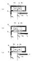
図4は、この発明の第2実施例に係るアンテナを示す概略平面図であり、図5は、直列回路の第1リアクタンス回路4aの具体例を示す回路図であり、図6は、可変の第2リアクタンス回路4bの具体例を示す回路図である。
この実施例のアンテナ1は、第1実施例の第1リアクタンス回路4a及び第2リアクタンス回路4bに対して具体的な可変の直列回路を適用したものである。
第1リアクタンス回路4aとしては、可変容量素子を含む直列回路又は可変容量素子を含む並列回路があるが、この実施例では、可変容量素子を含む直列回路を適用した。ところで、可変容量素子を含む直列回路としては、図5の(a)及び(b)に示す直列回路が挙げられる。この例では、図5の(a)の直列回路を適用した。
一方、第2リアクタンス回路4bとしては、可変容量素子を含む直列回路又は可変容量素子を含む並列回路や、固定容量素子を含む直列回路又は固定容量素子を含む並列回路があるが、この実施例では、可変容量素子を含む直列回路又は可変容量素子を含む並列回路を適用した。ところで、可変容量素子を含む直列回路又は可変容量素子を含む並列回路としては、図6の(a)〜(d)に示す回路が挙げられる。この例では、可変回路である図6の(a)の直列回路を適用した。
FIG. 4 is a schematic plan view showing an antenna according to a second embodiment of the present invention, FIG. 5 is a circuit diagram showing a specific example of the
In the
As the
On the other hand, as the
すなわち、図4に示すように、給電電極5に接続されたインダクタ41に、可変容量素子としての可変容量ダイオード42のアノード側を接続した直列回路で第1リアクタンス回路4aを構成し、放射電極6に接続されたインダクタ43に、可変容量素子としての可変容量ダイオード44のアノード側を接続した直列回路で第2リアクタンス回路4bを構成した。そして、これら可変容量ダイオード42,44の同極同士(カソード側同士)を接続し、その接続点Pを、高周波カット用抵抗121及びDCパスコンデンサ122を介して受信周波数制御部120に接続している。ところで、可変容量ダイオード42,44のアノード側の電位を共にゼロ電位にする必要があることから、インダクタ4cをインダクタ41の給電電極5側の端部とインダクタ43の放射電極6側の端部との間に接続した。
これにより、制御電圧Vcが受信周波数制御部120から周波数可変回路4の接続点Pに印加されると、可変容量ダイオード42,44の容量値が変化して、第1アンテナ部2の電気長が変化し、第1アンテナ部2の共振周波数が制御電圧Vcの大きさに対応した共振周波数に変位する。これと同時に、第2アンテナ部3の共振周波数も、可変容量ダイオード42のリアクタンス値の変化に対応して変位する。
That is, as shown in FIG. 4, the
Accordingly, when the control voltage Vc is applied from the reception
なお、この実施例では、直列接続回路である第1リアクタンス回路4aに接続される第2リアクタンス回路4bとして、インダクタ43と可変容量ダイオード44とを直列に接続した図6の(a)に示す回路を適用したが、これに限るものではなく、可変容量ダイオード44を含むあらゆる直列回路又は並列回路を適用することができる。したがって、第2リアクタンス回路4bとして、図6の(d)に示す並列回路のいずれをも適用することができる。
In this embodiment, as the
次に、この発明の第3実施例について説明する。
図7は、この発明の第3実施例に係るアンテナを示す概略平面図であり、図8は、固定の第2リアクタンス回路4bの具体例を示す回路図である。
上記第2実施例では、第1リアクタンス回路4aとして、可変容量素子を含む直列回路を適用し、第2リアクタンス回路4bとして、可変容量素子を含む直列回路又は可変容量素子を含む並列回路を適用したが、この実施例では、第2リアクタンス回路4bとして、固定容量素子を含む直列回路又は固定容量素子を含む並列回路を適用した。
ところで、固定容量素子を含む直列回路又は固定容量素子を含む並列回路としては、図8の(a)〜(e)に示す回路が挙げられる。この例では、固定回路である図8の(a)の直列回路を適用した。
Next explained is the third embodiment of the invention.
FIG. 7 is a schematic plan view showing an antenna according to a third embodiment of the present invention, and FIG. 8 is a circuit diagram showing a specific example of the fixed
In the second embodiment, a series circuit including a variable capacitance element is applied as the
Incidentally, examples of the series circuit including the fixed capacitance element or the parallel circuit including the fixed capacitance element include the circuits illustrated in FIGS. In this example, the series circuit of FIG. 8A which is a fixed circuit is applied.
具体的には、図7に示すように、周波数可変回路4の第1リアクタンス回路4aを、上記第1実施例と同様に、インダクタ41と可変容量ダイオード42との直列回路で構成し、第2リアクタンス回路4bを、固定容量素子としてのコンデンサ45とインダクタ43との直列回路で構成した。そして、第1リアクタンス回路4aの可変容量ダイオード42を第2リアクタンス回路4bのコンデンサ45に接続して、その接続点Pに、可変容量ダイオード42の容量を制御するための制御電圧Vcを印加するようにした。
Specifically, as shown in FIG. 7, the
かかる構成により、第2リアクタンス回路4bのリアクタンス値が固定であるので、高価な可変容量ダイオード44等を必要とせず、その分低コストで製造することができる。
その他の構成、作用及び効果は、上記第2実施例と同様であるので、その記載は省略する。
With such a configuration, since the reactance value of the
Other configurations, operations, and effects are the same as those of the second embodiment, and thus description thereof is omitted.
なお、この実施例では、直列接続回路である第1リアクタンス回路4aに接続される第2リアクタンス回路4bとして、インダクタ43とコンデンサ45とを直列に接続した図8の(a)に示す回路を適用したが、これに限るものではなく、コンデンサ45を含むあらゆる直列回路又は並列回路を適用することができる。したがって、第2リアクタンス回路4bとして、図8の(e)に示す並列回路を適用することもできる。すなわち、図9に示すように、インダクタ43とコンデンサ45とを並列に接続した並列回路で第2リアクタンス回路4bを構成し、可変容量ダイオード42のカソード側を第2リアクタンス回路4bに接続することで、この実施例と同様の作用効果を得ることができる。
In this embodiment, the circuit shown in FIG. 8A in which an
次に、この発明の第4実施例について説明する。
図10は、この発明の第4実施例に係るアンテナを示す概略平面図であり、図11は、並列回路の第1リアクタンス回路4aの具体例を示す回路図である。
上記第2及び第3実施例では、第1リアクタンス回路4aとして、可変容量素子を含む直列回路を適用したが、この実施例では、第1リアクタンス回路4aとして、可変容量素子を含む並列回路を適用した。
ところで、可変容量素子を含む並列回路としては、図11の(a)及び(b)に示す回路が挙げられる。この例では、図11の(a)の並列回路を適用した。
すなわち、図10に示すように、インダクタ47及び共用のコンデンサ48でなる直列回路を、インダクタ41及び可変容量ダイオード42でなる直列回路に並列に接続して、並列回路の第1リアクタンス回路4aを構成した。また、第2リアクタンス回路4bにおいても同様に、インダクタ46及び共用のコンデンサ48でなる直列回路を、インダクタ43及び可変容量ダイオード44でなる直列回路に並列に接続して、並列回路の第2リアクタンス回路4bを構成した。
そして、可変容量ダイオード42,44の同極同士を接続して、その接続点Pに可変容量ダイオード42,44の容量を制御するための制御電圧Vcを印加するようにした。
Next explained is the fourth embodiment of the invention.
FIG. 10 is a schematic plan view showing an antenna according to the fourth embodiment of the present invention, and FIG. 11 is a circuit diagram showing a specific example of the
In the second and third embodiments, a series circuit including a variable capacitance element is applied as the
By the way, as a parallel circuit including a variable capacitance element, the circuits shown in FIGS. In this example, the parallel circuit of FIG.
That is, as shown in FIG. 10, a series circuit composed of an
The same polarity of the
かかる構成により、周波数可変回路4の第1リアクタンス回路4aが並列回路になっているので、直列回路を用いた場合に比べて、第1リアクタンス回路4aのリアクタンス値を大きく変化させることができる。
また、インダクタ46,47のいずれかをチョークコイルとして用いることにより、第1及び第2リアクタンス回路4a,4bの一方を直列回路構成のリアクタンス回路とし、他方を並列回路構成のリアクタンス回路とすることができる。したがって、例えばインダクタ46をチョークコイルとして用いることで、第2アンテナ部3を、給電電極5とインダクタ41及び可変容量ダイオード42の直列回路と追加放射電極7とで構成することとなり、かかる条件下で、共振周波数f2の設定と可変範囲が決まることとなる。なお、コンデンサ48は、直流カット用のコンデンサとして機能する。
その他の構成、作用及び効果は、上記第2及び第3実施例と同様であるので、その記載は省略する。
With this configuration, since the
Further, by using one of the
Other configurations, operations, and effects are the same as those in the second and third embodiments, and thus description thereof is omitted.
なお、この実施例では、並列回路である第1リアクタンス回路4aに接続される第2リアクタンス回路4bとして、図8の(c)に示す並列回路を接続した例を示したが、これに限るものではなく、第2リアクタンス回路4bとして、図6及び図8に示すあらゆる回路を適用することができることは勿論である。したがって、図12に示すような変形が可能である。すなわち、第1リアクタンス回路4aと第2リアクタンス回路4bとの接続の組合せとして、図12の(a)に示すように、図11の(a)の並列回路と図6の(d)に示す可変並列回路の組合せや、図12の(b)に示すように、図11の(b)の並列回路と図8の(a)に示す固定直列回路の組合せ、及び図12の(c)に示すように、図11の(a)の並列回路と図8の(d)に示す固定並列回路の組合せ等を採用することができる。
In this embodiment, an example is shown in which the parallel circuit shown in FIG. 8C is connected as the
次に、この発明の第5実施例について説明する。
図13は、この発明の第5実施例に係るアンテナを示す概略平面図であり、図14は付加したインダクタの特性によって生じるリターンロス曲線図であり、図14の(a)は、インダクタをチョークコイルとして設定した場合を示し、図14の(b)は、インダクタを共振周波数調整用として設定した場合を示す。
この実施例は、図13に示すように、インダクタ40を周波数可変回路4の第1及び第2リアクタンス回路4a,4bを跨ぐように並列に付加した点が、上記第1ないし第4実施例と異なる。
ここでは、第1リアクタンス回路4aとして図5の(a)に示した可変直列回路を採用すると共に、第2リアクタンス回路4bとして、図6の(b)に示した可変回路を採用して構成した周波数可変回路4に、インダクタ40を並列に接続した例について説明する。
すなわち、インダクタ40を給電電極5と放射電極6との間に配し、その両端を、可変容量ダイオード42,44のカソード側にそれぞれ接続した。
Next explained is the fifth embodiment of the invention.
FIG. 13 is a schematic plan view showing an antenna according to a fifth embodiment of the present invention, FIG. 14 is a return loss curve diagram caused by the characteristics of the added inductor, and FIG. FIG. 14B shows the case where the inductor is set for adjusting the resonance frequency.
As shown in FIG. 13, this embodiment is different from the first to fourth embodiments in that an
Here, the variable series circuit shown in FIG. 5A is adopted as the
That is, the
したがって、インダクタ40をチョークコイルとして設定することで、雑音を帯域内から除去することができると共に、任意の共振周波数のみを大きく動かすことができる。これにより、図14の(a)の実線リターンロス曲線S1及び破線リターンロス曲線S2で示すように、共振周波数f1の変化量M1が共振周波数f2の変化量M2よりも大きくなるように、共振周波数f1のみを大きく変化させることができる。
Therefore, by setting the
また、インダクタ40を共振周波数調整用インダクタとして設定することで、給電電極5とこのインダクタ40と放射電極6とでなる第3のアンテナ部を構成することができる。この結果、図14の(b)の実線リターンロス曲線S1に示すように、第1アンテナ部2の共振周波数f1よりも低い周波数領域に、この第3のアンテナ部による新たな共振周波数f0を生成して、その低い帯域を確保することができる。また、破線リターンロス曲線S2に示すように、インダクタ40のインダクタンス値を調整することで、第3のアンテナ部の共振周波数f0を任意に変化させることができる。
その他の構成、作用及び効果は、上記第1ないし第4実施例と同様であるので、その記載は省略する。
In addition, by setting the
Other configurations, operations, and effects are the same as those in the first to fourth embodiments, and thus description thereof is omitted.
なお、この実施例では、第1リアクタンス回路4aとして、図5の(a)に示した可変直列回路を採用すると共に、第2リアクタンス回路4bとして、図6の(b)に示した可変回路を採用して、周波数可変回路4を構成したが、インダクタ40を第1及び第2リアクタンス回路4a,4bを跨ぐように並列に付加してあればよく、周波数可変回路4の構造に限定はない。したがって、図15に示すようなアンテナを考えることができる。
すなわち、図15の(a)に示すように、上記第2実施例で適用した構造の周波数可変回路4に、インダクタ40を並列に接続しても、この実施例と同様の作用効果を得ることができる。また、図15の(b)に示すように、第2リアクタンス回路4bに、インダクタ43とコンデンサ45との直列回路を採用しても、この実施例と同様の作用効果を得ることができる。
In this embodiment, the variable series circuit shown in FIG. 5A is adopted as the
That is, as shown in FIG. 15 (a), even if the
次に、この発明の第6実施例について説明する。
図16は、この発明の第6実施例に係るアンテナを示す概略平面図である。
この実施例は、上記第4実施例において、第2アンテナ部3の追加放射電極7とは別体の追加放射電極7′を共振周波数調整用インダクタ71を介して接続点Pに接続すると共に、追加放射電極6′を共振周波数調整用インダクタ61を介して放射電極6に接続した構成とした。そして、制御電圧Vcを接続点Pに印加するようにした。
これにより、給電電極5と第1リアクタンス回路4aと共振周波数調整用インダクタ71と追加放射電極7′とで第3のアンテナ部が形成されると共に、給電電極5と周波数可変回路4と追加放射電極6′とによって第4のアンテナ部が形成され、4共振のアンテナを実現することができる。すなわち、さらなる多共振化が可能となり、マルチメディアに対応したマルチバンドのアンテナを提供することができる。
その他の構成、作用及び効果は、上記実施例と同様であるので、その記載は省略する。
Next explained is the sixth embodiment of the invention.
FIG. 16 is a schematic plan view showing an antenna according to the sixth embodiment of the present invention.
In this embodiment, in the fourth embodiment, an
As a result, a third antenna portion is formed by the feeding
Since other configurations, operations, and effects are the same as those in the above-described embodiment, description thereof is omitted.
次に、この発明の第7実施例について説明する。
図17は、この発明の第7実施例に係るアンテナを示す斜視図である。
この実施例は、給電電極5と周波数可変回路4と放射電極6と追加放射電極7等のアンテナ要素を所定の誘電体基体上に形成した構成とする。
この実施例では、図17に示すように、図15の(a)に示したアンテナを誘電体基体8表面に形成した例について説明する。
Next, a seventh embodiment of the present invention will be described.
FIG. 17 is a perspective view showing an antenna according to the seventh embodiment of the present invention.
In this embodiment, antenna elements such as the feeding
In this embodiment, as shown in FIG. 17, an example in which the antenna shown in FIG. 15A is formed on the surface of the
具体的には、誘電体基体8は、正面80と両側面81,82と上面83と下面84と裏面85とを有する直方体状をなし、回路基板100の非グランド領域101上に載置されている。
そして、給電電極5が、この誘電体基体8の左側において、正面80から上面83に亘ってパターン形成されている。非グランド領域101上には、パターン113が形成され、インダクタ112を通じて送受信部110に接続されている。そして、給電電極5の一方の端部5aがこのパターン113に接続され、他方の端部5bが周波数可変回路4に接続されている。この周波数可変回路4において、第1リアクタンス回路4aのインダクタ41及び可変容量ダイオード42と第2リアクタンス回路4bのインダクタ43及び可変容量ダイオード44は、それぞれチップ部品であり、上面83上に形成されたパターン48を介して接続されている。
そして、インダクタ40が、この第1リアクタンス回路4a及び第2リアクタンス回路4bを跨ぐようにして、上面83上に形成されている。すなわち、パターン48と平行なパターン49が形成され、このパターン49の途中にインダクタ40が介設されている。
放射電極6は、パターン48,49の接続部から上面83の上隅を右方に延び、側面81を下降した電極部6aを有する。そして、電極部6bが、電極部6aと連続した状態で、下面84の左方に延び、側面82を上昇している。そして、この電極部6bの上端が、上面83上に隅に形成された電極部6cに連結している。すなわち、放射電極6は、電極部6a〜6cで成り、全体としてループ形状をなす。
また、周波数可変回路4の可変容量ダイオード42,44との接続部からは、パターン72が引き出され、上面83及び正面80を伝わって、非グランド領域101上の形成され受信周波数制御部120に至るパターン123と接続している。そして、パターン72の途中に、高周波カット用抵抗121が介設されている。
追加放射電極7は、上記のようなパターン72に対して垂直方向を向くように、パターン形成され、共振周波数調整用インダクタ70を介してパターン72に接続されている。
Specifically, the
The
An
The
Further, the
The
かかる構成により、誘電体基体8の誘電率を変化させることにより、第1及び第2アンテナ部2,3のリアクタンス値を調整することができる。
その他の構成、作用及び効果は、上記第1ないし第6実施例と同様であるので、その記載は省略する。
なお、この実施例では、給電電極5等のアンテナ要素のほぼ全てを誘電体基体8に形成したが、アンテナ要素の一部を誘電体基体8に形成しても良い。また、この実施例では、図15の(a)に示したアンテナを誘電体基体8表面に形成したが、これに限るものではなく、上記した全ての実施例のアンテナを誘電体基体8表面に形成することができることは勿論である。
With this configuration, the reactance values of the first and
Other configurations, operations, and effects are the same as those in the first to sixth embodiments, and thus description thereof is omitted.
In this embodiment, almost all of the antenna elements such as the feeding
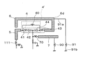
次に、この発明の第8実施例について説明する。
図18は、この発明の第8実施例に係るアンテナを示す概略平面図であり、図19は付加したインダクタの特性によって生じるリターンロス曲線図である。
この実施例は、図18に示すように、第2アンテナ部3の追加放射電極7の途中に単体のインダクタ90を接続した点が、上記実施例とは異なる。
具体的には、インダクタ90の一方端90aを追加放射電極7の先端部側に接続すると共に、他方端90bをグランド領域102(図1参照)に接続した。
Next, an eighth embodiment of the present invention will be described.
FIG. 18 is a schematic plan view showing an antenna according to the eighth embodiment of the present invention, and FIG. 19 is a return loss curve diagram caused by the characteristics of the added inductor.
As shown in FIG. 18, this embodiment is different from the above embodiment in that a
Specifically, one end 90a of the
かかる構成により、図19のリターンロス曲線S1で示すように、インダクタ111と給電電極5と周波数可変回路部分4′とによる共振周波数がf0であり、インダクタ111と給電電極5と周波数可変回路4と放射電極6とによる共振周波数がf1であり、インダクタ111と給電電極5と周波数可変回路4と共振周波数調整用インダクタ70と追加放射電極7とによる共振周波数がf2であるとすると、インダクタ111と給電電極5と周波数可変回路4と共振周波数調整用インダクタ70と追加放射電極7とインダクタ90とによる共振周波数faが新たに生成される。
インダクタ90としては、追加放射電極7とグランド領域102に接続した状態で、高インピーダンスとなるインダクタが選択されており、これにより、アンテナ利得の劣化を防止している。そして、このように高インピーダンスのインダクタ90を採用することで、インダクタ111と給電電極5と周波数可変回路4と共振周波数調整用インダクタ70と追加放射電極7とによる共振周波数f2に大きな影響を与えることなく、分岐元の追加放射電極7が持つ周波数より低い周波数である新たな共振周波数faを生成することができる。かかる低周波の共振周波数を電極のみで形成する場合には、相当長い電極を用いなければならず、アンテナ体積が大きくなってしまう。しかし、この実施例のように、電極を用いずにインダクタ90で新たな共振周波数faを生成することで、アンテナ体積の小型化を図ることができる。
また、可変容量ダイオード42,44を含む周波数可変回路4が給電電極5と放射電極6との間及び給電電極5と追加放射電極7との間に介在しているので、制御電圧Vcを周波数可変回路4に印加することで、図19の破線で示すリターンロス曲線S2のように、共振周波数f0,fa,f1,f2を全体的に変化させることができる。
そして、共振周波数f0,fa,f1,f2を適宜設定することで、FMの電波,VHF帯の電波,及びUHF帯の電波が受信可能となる。
その他の構成、作用及び効果は、上記実施例と同様であるので、その記載は省略する。
With this configuration, as shown by the return loss curve S1 in FIG. 19, the resonance frequency of the
As the
Further, since the frequency
Then, by appropriately setting the resonance frequencies f0, fa, f1, and f2, it is possible to receive FM radio waves, VHF band radio waves, and UHF band radio waves.
Since other configurations, operations, and effects are the same as those in the above-described embodiment, description thereof is omitted.
なお、この実施例では、インダクタ90を第2アンテナ部の追加放射電極7の途中に接続した構成としたが、インダクタ90を追加放射電極7の開放先端部7a側に設けても良い。但し、インダクタ90を開放先端部7a側に近づけすぎると、アンテナ利得が劣化するおそれがあるので、この点を留意して、インダクタ90を追加放射電極7に接続することが好ましい。
また、この実施例では、インダクタ90を第2アンテナ部の追加放射電極7にのみ接続した構成としたが、インダクタ90を追加放射電極7に接続せず、第1アンテナ部2の放射電極6の途中にのみ接続しても良い。
さらに、この実施例では、インダクタ90に1つのインダクタ90を接続したが、これに限らず、複数のインダクタ90を並列に接続することもできる。
In this embodiment, the
In this embodiment, the
Furthermore, in this embodiment, one
次に、この発明の第9実施例について説明する。
図20は、この発明の第9実施例に係るアンテナを示す概略平面図であり、図21は、付加した2つのインダクタの特性によって生じるリターンロス曲線図である。
この実施例は、図20に示すように、第1アンテナ部2の放射電極6の途中にも単体のインダクタ91を接続した点が、上記第8実施例とは異なる。
具体的には、インダクタ91の一方端91aを放射電極6の折曲部6dに接続すると共に、他方端91bをグランド領域102に接続した。
これにより、図21のリターンロス曲線S1で示すように、インダクタ111と給電電極5と周波数可変回路部分4′とによる共振周波数f0、インダクタ111と給電電極5と周波数可変回路4と共振周波数調整用インダクタ70と追加放射電極7とインダクタ90とによる共振周波数fa、インダクタ111と給電電極5と周波数可変回路4と放射電極6とによる共振周波数f1、インダクタ111と給電電極5と周波数可変回路4と共振周波数調整用インダクタ70と追加放射電極7とによる共振周波数f2の他に、インダクタ111と給電電極5と周波数可変回路4と放射電極6とインダクタ91とによって、分岐元の放射電極6が持つ周波数より低い周波数である新たな共振周波数fbが新たに生成される。
このインダクタ91もインダクタ90と同様に高インピーダンスなインダクタであり、
共振周波数fbは、共振周波数faとf1との間に位置する低い共振周波数である。
そして、制御電圧Vcを周波数可変回路4に印加することで、図21の破線で示すリターンロス曲線S2のように、共振周波数f0,fa,fb,f1,f2を全体的に変化させることができる。
その他の構成、作用及び効果は、上記第8実施例と同様であるので、その記載は省略する。
Next, a ninth embodiment of the present invention will be described.
FIG. 20 is a schematic plan view showing an antenna according to a ninth embodiment of the present invention, and FIG. 21 is a return loss curve diagram caused by the characteristics of the two added inductors.
As shown in FIG. 20, this embodiment is different from the eighth embodiment in that a
Specifically, one
Accordingly, as shown by the return loss curve S1 in FIG. 21, the resonance frequency f0 by the
This
The resonance frequency fb is a low resonance frequency located between the resonance frequencies fa and f1.
Then, by applying the control voltage Vc to the frequency
Other configurations, operations, and effects are the same as those in the eighth embodiment, and thus description thereof is omitted.
次に、この発明の第10実施例について説明する。
図22は、この発明の第10実施例に係るアンテナを示す概略平面図であり、図23は、付加した3つのインダクタの特性によって生じるリターンロス曲線図である。
この実施例は、図22に示すように、第2アンテナ部3の追加放射電極7とは別体の追加放射電極6′,7′が設けられたアンテナにおいて、追加放射電極6′,7′にも、単体のインダクタ92,93をそれぞれ接続した点が、上記第8及び第9実施例とは異なる。
具体的には、インダクタ92の一方端92aを放射電極6の折曲部6eに接続すると共に、他方端92bをグランド領域102に接続した。そして、インダクタ93の一方端93aを追加放射電極7′の開放先端に接続すると共に、他方端93bをグランド領域102に接続した。
これにより、図23のリターンロス曲線S1で示すように、共振周波数f0,fa,f1,f2の他に、インダクタ111と給電電極5と周波数可変回路4と放射電極6と共振周波数調整用インダクタ61と追加放射電極6′とインダクタ92とによって、分岐元の追加放射電極6′が持つ周波数より低い周波数である新たな共振周波数fbが新たに生成され、インダクタ111と給電電極5と周波数可変回路4と共振周波数調整用インダクタ71と追加放射電極7′とインダクタ93とによって、分岐元の追加放射電極7′が持つ周波数より低い周波数である新たな共振周波数fcが新たに生成される。
これらのインダクタ92,93もインダクタ90,91と同様に高インピーダンスなインダクタであり、共振周波数fbは、共振周波数faとf1との間に位置する低い周波数であり、共振周波数fcは、共振周波数f0とfaとの間に位置する低い周波数である。
そして、制御電圧Vcを周波数可変回路4に印加することで、図23の破線で示すリターンロス曲線S2のように、共振周波数f0,fc,fa,fb,f1,f2を全体的に変化させることができる。
その他の構成、作用及び効果は、上記第8及び第9実施例と同様であるので、その記載は省略する。
Next, a tenth embodiment of the present invention will be described.
FIG. 22 is a schematic plan view showing an antenna according to the tenth embodiment of the present invention, and FIG. 23 is a return loss curve diagram caused by the characteristics of the three added inductors.
In this embodiment, as shown in FIG. 22, in an antenna provided with additional radiation electrodes 6 'and 7' separate from the
Specifically, one
Accordingly, as shown by the return loss curve S1 in FIG. 23, in addition to the resonance frequencies f0, fa, f1, and f2, the
These
Then, by applying the control voltage Vc to the frequency
Other configurations, operations, and effects are the same as those in the eighth and ninth embodiments, and thus description thereof is omitted.
次に、この発明の第11実施例について説明する。
図24は、この発明の第11実施例に係るアンテナを示す概略平面図であり、図25は、付加した直列共振回路の特性によって生じるリターンロス曲線図であり、図26は、インダクタ単体のリアクタンスと直列共振回路のリアクタンスとを比較して示す線図である。
この実施例は、図24に示すように、第2アンテナ部3の追加放射電極7に、リアクタンス回路としての直列共振回路9を接続した点が、上記第8ないし第10実施例と異なる。
具体的には、直列共振回路9を直列接続されたインダクタ94とコンデンサ95とで構成し、インダクタ94の一方端94aを追加放射電極7の先端部側に接続すると共に、コンデンサ95の一方端95aをグランド領域102に接続した。
これにより、図25のリターンロス曲線S1で示すように、共振周波数f0,f1,f2の他に、インダクタ111と給電電極5と周波数可変回路4と共振周波数調整用インダクタ70と追加放射電極7と直列共振回路9による共振周波数faが新たに生成される。
そして、制御電圧Vcを周波数可変回路4に印加することで、図25の破線で示すリターンロス曲線S2のように、共振周波数f0,fa,f1,f2を全体的に変化させることができる。
Next, an eleventh embodiment of the present invention will be described.
FIG. 24 is a schematic plan view showing an antenna according to an eleventh embodiment of the present invention, FIG. 25 is a return loss curve diagram caused by the characteristics of the added series resonance circuit, and FIG. 26 is a reactance of a single inductor. It is a diagram which shows and compares the reactance of a series resonant circuit.
As shown in FIG. 24, this embodiment differs from the eighth to tenth embodiments in that a
Specifically, the
As a result, as shown by the return loss curve S1 in FIG. 25, in addition to the resonance frequencies f0, f1, and f2, the
Then, by applying the control voltage Vc to the frequency
ところで、図26のリアクタンス曲線R1に示すように、直列共振回路9のような直列共振回路では、リアクタンス曲線R2で示すインダクタ90〜93のようなインダクタ単体に比べて、周波数に対するリアクタンスの変化勾配が大きい。したがって、追加共振に必要なインダクタ単体のリアクタンスと直列共振回路のリアクタンスとが同値であれば、分岐元の電極(この実施例では追加放射電極7)が持つ共振周波数でのリアクタンスは、インダクタ単体の場合と比べて直列共振回路の方が大きくなる。すなわち、この実施例において、インダクタ90の代わりに直列共振回路9を追加放射電極7に接続することで、インダクタ111と給電電極5と周波数可変回路4と共振周波数調整用インダクタ70と追加放射電極7とよる共振周波数f2に大きな影響を与えることなく、新たな共振周波数faを得ることができ、この結果、動作特性に優れたアンテナを提供することができる。
その他の構成、作用及び効果は、上記第8ないし第10実施例と同様であるので、その記載は省略する。
Incidentally, as shown in the reactance curve R1 of FIG. 26, in the series resonance circuit such as the
Other configurations, operations, and effects are the same as those in the eighth to tenth embodiments, and thus description thereof is omitted.
次に、この発明の第12実施例について説明する。
図27は、この発明の第12実施例に係るアンテナを示す概略平面図であり、図28は、付加した直列共振回路の特性によって生じるリターンロス曲線図である。
この実施例は、図27に示すように、第2アンテナ部3の追加放射電極7に、リアクタンス回路としての並列共振回路9′を接続した点が、上記第11実施例と異なる。
具体的には、並列共振回路9′を並列接続されたインダクタ94′とコンデンサ95′とで構成し、並列共振回路9′の一方端9a′を追加放射電極7の先端部側に接続すると共に、他方端の一方端9b′をグランド領域102に接続した。
これにより、図28のリターンロス曲線S1で示すように、共振周波数f0,f1,f2の他に、インダクタ111と給電電極5と周波数可変回路4と共振周波数調整用インダクタ70と追加放射電極7と並列共振回路9′による共振周波数faが新たに生成される。
そして、制御電圧Vcを周波数可変回路4に印加することで、図28の破線で示すリターンロス曲線S2のように、共振周波数f0,fa,f1,f2を全体的に変化させることができる。
Next, a twelfth embodiment of the present invention will be described.
FIG. 27 is a schematic plan view showing an antenna according to the twelfth embodiment of the present invention, and FIG. 28 is a return loss curve diagram caused by the characteristics of the added series resonance circuit.
As shown in FIG. 27, this embodiment is different from the eleventh embodiment in that a parallel resonance circuit 9 'as a reactance circuit is connected to the
Specifically, the parallel
As a result, as shown by the return loss curve S1 in FIG. 28, in addition to the resonance frequencies f0, f1, and f2, the
Then, by applying the control voltage Vc to the frequency
ところで、上記第11実施例の直列共振回路9で大きなリアクタンスを得るためには、定数(nH)の大きなインダクタ94を用いる必要がある。一般には、インダクタ94としてはチップ部品を用いる。そして、大きな定数のチップ部品を用いると、自己共振周波数が下がり、その誘導性が劣化する。これに対して、この実施例のように、並列共振回路9′を用いることで、小さな定数のインダクタ94′で大きなリアクタンスを得ることができる。したがって、並列共振回路9′を用いることで、チップ部品が抱える自己共振周波数の問題を解決することができる。
その他の構成、作用及び効果は、上記第11実施例と同様であるので、その記載は省略する。
Incidentally, in order to obtain a large reactance in the
Other configurations, operations, and effects are the same as those in the eleventh embodiment, and thus description thereof is omitted.
次に、この発明の第13実施例について説明する。
図29は、この発明の第13実施例に係るアンテナを示す概略平面図であり、図30は、付加した直列共振回路の特性によって生じるリターンロス曲線図である。
この実施例は、図29に示すように、第2アンテナ部3の追加放射電極7に、リアクタンス回路として、直列共振回路9と並列共振回路9′との複合回路10を接続した点が、上記第11及び第12実施例と異なる。
具体的には、直列共振回路9と並列共振回路9′とを直列に接続して、複合回路10を構成し、直列共振回路9のインダクタ94の一方端94aを追加放射電極7の先端部側に接続すると共に、並列共振回路9′の一方端9b′をグランド領域102に接続した。
これにより、図30のリターンロス曲線S1で示すように、共振周波数f0,f1,f2の他に、インダクタ111と給電電極5と周波数可変回路4と共振周波数調整用インダクタ70と追加放射電極7と複合回路10による共振周波数faが新たに生成される。
そして、制御電圧Vcを周波数可変回路4に印加することで、図30の破線で示すリターンロス曲線S2のように、共振周波数f0,fa,f1,f2を全体的に変化させることができる。
Next, a thirteenth embodiment of the present invention will be described.
FIG. 29 is a schematic plan view showing an antenna according to the thirteenth embodiment of the present invention, and FIG. 30 is a return loss curve diagram caused by the characteristics of the added series resonance circuit.
In this embodiment, as shown in FIG. 29, the
Specifically, the series
As a result, as shown by the return loss curve S1 in FIG. 30, in addition to the resonance frequencies f0, f1, and f2, the
Then, by applying the control voltage Vc to the frequency
かかる構成により、追加放射電極7による共振周波数f2に大きな影響を与えることなく、新たな共振周波数faを得ることができるという直列共振回路9の利点と、インダクタチップ部品が抱える自己共振周波数の問題を解決することができるという並列共振回路9′の利点との双方を享受することができる。
その他の構成、作用及び効果は、上記第11及び第12実施例と同様であるので、その記載は省略する。
With this configuration, there are the advantages of the
Other configurations, operations, and effects are the same as those in the eleventh and twelfth embodiments, and thus the description thereof is omitted.
なお、この発明は、上記実施例に限定されるものではなく、発明の要旨の範囲内において種々の変形や変更が可能である。
例えば、上記実施例では、追加放射電極を共振周波数調整用インダクタを介して周波数可変回路4の接続点Pや放射電極6の途中に接続した例を挙げて説明したが、図31に示すように、第2アンテナ部3を構成する追加放射電極7とは別体の追加放射電極6′を放射電極6の途中に直接形成することもできる。
In addition, this invention is not limited to the said Example, A various deformation | transformation and change are possible within the range of the summary of invention.
For example, in the above embodiment, the example has been described in which the additional radiation electrode is connected to the connection point P of the frequency
1…アンテナ、 2…第1アンテナ部、 3…第2アンテナ部、 4…周波数可変回路、 4a…第1リアクタンス回路、 4b…第2リアクタンス回路、 5…給電電極、 6…放射電極、 6′,7,7′…追加放射電極、 9…直列共振回路、 9′…並列共振回路、 10…複合回路、 40,41,43,46,47,90〜94,94′,111,112…インダクタ、 42,44…可変容量ダイオード、 45,48,95,95′…コンデンサ、 60…開放先端、 61,70,71…共振周波数調整用インダクタ、 100…回路基板、 101…非グランド領域、 102…グランド領域、 110…送受信部、 120…受信周波数制御部、 121,DC…高周波カット用抵抗、 122…パスコンデンサ、 G…間隔、 M,M1,M2…変化量、 P…接続点、 Vc…制御電圧、 f0,fa,fb,fc,f1,f2…共振周波数。
DESCRIPTION OF
Claims (16)
上記周波数可変回路を、上記給電電極に接続され且つそのリアクタンス値を直流の制御電圧で変化可能な第1リアクタンス回路に、上記第1アンテナ部の放射電極に接続された第2リアクタンス回路を直列に接続して構成し、
上記第2アンテナ部の追加放射電極を、上記第1及び第2リアクタンス回路の接続点から分岐することにより、
上記第1アンテナ部を、上記給電電極と第1リアクタンス回路と第2リアクタンス回路と放射電極とで構成し、
上記第2アンテナ部を、上記給電電極と第1リアクタンス回路と追加放射電極とで構成した、
ことを特徴とするアンテナ。A second antenna comprising a first antenna portion formed by connecting a radiation electrode having an open end to a power supply electrode via a frequency variable circuit, an additional radiation electrode having an open end connected in the middle of the frequency variable circuit, and the power supply electrode. An antenna comprising an antenna unit,
The frequency variable circuit is connected in series to a first reactance circuit connected to the power supply electrode and the reactance value of which can be changed by a DC control voltage, and a second reactance circuit connected to the radiation electrode of the first antenna unit. Connect and configure,
By branching the additional radiation electrode of the second antenna part from the connection point of the first and second reactance circuits ,
The first antenna unit is composed of the feeding electrode, a first reactance circuit, a second reactance circuit, and a radiation electrode,
The second antenna part is composed of the feeding electrode, the first reactance circuit, and an additional radiation electrode.
An antenna characterized by that.
ことを特徴とする請求項1に記載のアンテナ。The second reactance circuit can change its reactance value with the control voltage.
The antenna according to claim 1.
ことを特徴とする請求項1に記載のアンテナ。The reactance value of the second reactance circuit is a fixed value.
The antenna according to claim 1.
上記第2リアクタンス回路は、可変容量素子を含む直列回路又は可変容量素子を含む並列回路であり、
上記第1及び第2リアクタンス回路の可変容量素子の同極同士を接続して上記第1及び第2リアクタンス回路の接続点とし、上記可変容量素子の容量を制御するための上記制御電圧をこの接続点に印加する、
ことを特徴とする請求項2に記載のアンテナ。The first reactance circuit is a series circuit including a variable capacitance element or a parallel circuit including a variable capacitance element,
The second reactance circuit is a series circuit including a variable capacitance element or a parallel circuit including a variable capacitance element,
The same polarity of the variable capacitance elements of the first and second reactance circuits are connected to serve as a connection point of the first and second reactance circuits, and the control voltage for controlling the capacitance of the variable capacitance elements is connected to the connection. Apply to point,
The antenna according to claim 2.
上記第2リアクタンス回路は、固定容量素子を含む直列回路又は固定容量素子を含む並列回路であり、
上記第1リアクタンス回路の可変容量素子を上記第2リアクタンス回路に接続して上記第1及び第2リアクタンス回路の接続点とし、上記可変容量素子の容量を制御するための上記制御電圧をこの接続点に印加する、
ことを特徴とする請求項3に記載のアンテナ。The first reactance circuit is a series circuit including a variable capacitance element or a parallel circuit including a variable capacitance element,
The second reactance circuit is a series circuit including a fixed capacitance element or a parallel circuit including a fixed capacitance element,
The variable capacitance element of the first reactance circuit is connected to the second reactance circuit to be a connection point of the first and second reactance circuits, and the control voltage for controlling the capacitance of the variable capacitance element is connected to the connection point. Apply to
The antenna according to claim 3.
ことを特徴とする請求項1ないし請求項5のいずれかに記載のアンテナ。An inductor is connected in parallel to the first and second reactance circuits so as to straddle the first reactance circuit and the second reactance circuit.
The antenna according to any one of claims 1 to 5, wherein
ことを特徴とする請求項1ないし請求項6のいずれかに記載のアンテナ。The additional radiation electrode branches from the connection point via an inductor for controlling the resonance frequency,
The antenna according to any one of claims 1 to 6, wherein the antenna is provided.
ことを特徴とする請求項1ないし請求項7のいずれかに記載のアンテナ。One or more additional radiation electrodes that are separate from the additional radiation electrode are branched from the connection point,
The antenna according to any one of claims 1 to 7, characterized in that
ことを特徴とする請求項1ないし請求項8のいずれかに記載のアンテナ。An additional radiation electrode separate from the additional radiation electrode was connected in the middle of the radiation electrode,
The antenna according to any one of claims 1 to 8, wherein
ことを特徴とする請求項9に記載のアンテナ。The separate additional radiation electrode is connected to the radiation electrode via an inductor,
The antenna according to claim 9.
ことを特徴とする請求項1ないし請求項10のいずれかに記載のアンテナ。The first antenna portion has a loop shape in which the feeding electrode and the open tip of the radiation electrode are arranged to face each other with a gap therebetween.
The antenna according to any one of claims 1 to 10, wherein
ことを特徴とする請求項1ないし請求項11のいずれかに記載のアンテナ。All or part of the antenna elements such as the feeding electrode, the frequency variable circuit, the radiation electrode, and the additional radiation electrode are formed on the dielectric substrate.
The antenna according to any one of claims 1 to 11, characterized in that:
ことを特徴とする請求項1ないし請求項12のいずれかに記載のアンテナ。One or all of the radiation electrode of the first antenna part, the additional radiation electrode of the second antenna part, and the one or more separate additional radiation electrodes, or in the middle or open of the electrode The tip was connected to ground via a single inductor or a reactance circuit.
The antenna according to any one of claims 1 to 12, wherein the antenna is provided.
ことを特徴とする請求項13に記載のアンテナ。The reactance circuit is either a series resonant circuit or a parallel resonant circuit, or a composite circuit of these series resonant circuit and parallel resonant circuit.
The antenna according to claim 13.
ことを特徴とする請求項13又は請求項14に記載のアンテナ。FM radio waves, VHF band radio waves, and UHF band radio waves can be received.
The antenna according to claim 13 or claim 14, wherein
ことを特徴とする無線通信機。The antenna according to any one of claims 1 to 15 is provided.
A wireless communication device.
Applications Claiming Priority (5)
| Application Number | Priority Date | Filing Date | Title |
|---|---|---|---|
| JP2005020199 | 2005-01-27 | ||
| JP2005020199 | 2005-01-27 | ||
| JP2005241890 | 2005-08-23 | ||
| JP2005241890 | 2005-08-23 | ||
| PCT/JP2005/022342 WO2006080141A1 (en) | 2005-01-27 | 2005-12-06 | Antenna and wireless communication device |
Publications (2)
| Publication Number | Publication Date |
|---|---|
| JPWO2006080141A1 JPWO2006080141A1 (en) | 2008-06-19 |
| JP4508190B2 true JP4508190B2 (en) | 2010-07-21 |
Family
ID=36740175
Family Applications (1)
| Application Number | Title | Priority Date | Filing Date |
|---|---|---|---|
| JP2006523881A Active JP4508190B2 (en) | 2005-01-27 | 2005-12-06 | Antenna and wireless communication device |
Country Status (5)
| Country | Link |
|---|---|
| US (1) | US7375695B2 (en) |
| EP (1) | EP1843432B1 (en) |
| JP (1) | JP4508190B2 (en) |
| CN (2) | CN103022704B (en) |
| WO (1) | WO2006080141A1 (en) |
Cited By (1)
| Publication number | Priority date | Publication date | Assignee | Title |
|---|---|---|---|---|
| US8552916B2 (en) | 2009-11-27 | 2013-10-08 | Fujitsu Limited | Antenna and radio communication apparatus |
Families Citing this family (124)
| Publication number | Priority date | Publication date | Assignee | Title |
|---|---|---|---|---|
| DE102004001899A1 (en) * | 2004-01-14 | 2005-08-11 | Md Elektronik Gmbh | Trap arrangement |
| FI20055420A0 (en) | 2005-07-25 | 2005-07-25 | Lk Products Oy | Adjustable multi-band antenna |
| FI119009B (en) | 2005-10-03 | 2008-06-13 | Pulse Finland Oy | Multiple-band antenna |
| FI118782B (en) | 2005-10-14 | 2008-03-14 | Pulse Finland Oy | Adjustable antenna |
| US20070248116A1 (en) | 2006-04-21 | 2007-10-25 | Masashi Hamada | Communication control apparatus and method of controlling same |
| WO2008007606A1 (en) * | 2006-07-11 | 2008-01-17 | Murata Manufacturing Co., Ltd. | Antenna and radio ic device |
| US8618990B2 (en) | 2011-04-13 | 2013-12-31 | Pulse Finland Oy | Wideband antenna and methods |
| WO2008078437A1 (en) * | 2006-12-22 | 2008-07-03 | Murata Manufacturing Co., Ltd. | Antenna structure and wireless communication apparatus with that antenna structure |
| EP2104178A4 (en) * | 2007-01-19 | 2014-05-28 | Murata Manufacturing Co | Antenna unit and wireless communication apparatus |
| US7573425B2 (en) | 2007-03-20 | 2009-08-11 | Industrial Technology Research Institute | Antenna for radio frequency identification RFID tags |
| FI20075269A0 (en) | 2007-04-19 | 2007-04-19 | Pulse Finland Oy | Method and arrangement for antenna matching |
| KR100867527B1 (en) | 2007-05-30 | 2008-11-06 | 삼성전기주식회사 | Tunable loop antenna |
| JP2009049868A (en) * | 2007-08-22 | 2009-03-05 | Hitachi Cable Ltd | Tuning type antenna module with frequency correction circuit and manufacturing method thereof |
| EP2182583B1 (en) * | 2007-08-24 | 2016-08-10 | Murata Manufacturing Co. Ltd. | Antenna apparatus and radio communication device |
| FI120427B (en) | 2007-08-30 | 2009-10-15 | Pulse Finland Oy | Adjustable multiband antenna |
| KR20120102173A (en) * | 2007-09-13 | 2012-09-17 | 퀄컴 인코포레이티드 | Antennas for wireless power applications |
| TWI420741B (en) * | 2008-03-14 | 2013-12-21 | Advanced Connectek Inc | Multi-antenna module |
| TWI411158B (en) * | 2008-04-09 | 2013-10-01 | Acer Inc | A multiband folded loop antenna |
| TWI359530B (en) * | 2008-05-05 | 2012-03-01 | Acer Inc | A coupled-fed multiband loop antenna |
| JP5009240B2 (en) * | 2008-06-25 | 2012-08-22 | ソニーモバイルコミュニケーションズ株式会社 | Multiband antenna and wireless communication terminal |
| JP2010041071A (en) * | 2008-07-31 | 2010-02-18 | Toshiba Corp | Antenna device |
| WO2010016298A1 (en) * | 2008-08-05 | 2010-02-11 | 株式会社村田製作所 | Antenna and wireless communication machine |
| WO2010044086A1 (en) * | 2008-10-13 | 2010-04-22 | Galtronics Corporation Ltd. | Multi-band antennas |
| JP5131481B2 (en) * | 2009-01-15 | 2013-01-30 | 株式会社村田製作所 | ANTENNA DEVICE AND RADIO COMMUNICATION DEVICE |
| US8339322B2 (en) | 2009-02-19 | 2012-12-25 | Galtronics Corporation Ltd. | Compact multi-band antennas |
| US8593348B2 (en) | 2009-04-07 | 2013-11-26 | Galtronics Corporation Ltd. | Distributed coupling antenna |
| JP5287474B2 (en) * | 2009-04-24 | 2013-09-11 | 株式会社村田製作所 | Antenna device |
| JP5003729B2 (en) * | 2009-06-18 | 2012-08-15 | 株式会社村田製作所 | Antenna and wireless communication device |
| JP5321290B2 (en) * | 2009-06-30 | 2013-10-23 | 株式会社村田製作所 | Antenna structure |
| US20120249387A1 (en) | 2009-11-02 | 2012-10-04 | Galtronics Corporation Ltd. | Distributed reactance antenna |
| FI20096134A0 (en) | 2009-11-03 | 2009-11-03 | Pulse Finland Oy | Adjustable antenna |
| JP5399866B2 (en) * | 2009-11-16 | 2014-01-29 | 三菱電線工業株式会社 | Antenna device substrate and antenna device |
| FI20096251A0 (en) | 2009-11-27 | 2009-11-27 | Pulse Finland Oy | MIMO antenna |
| US8847833B2 (en) | 2009-12-29 | 2014-09-30 | Pulse Finland Oy | Loop resonator apparatus and methods for enhanced field control |
| FI20105158A (en) * | 2010-02-18 | 2011-08-19 | Pulse Finland Oy | SHELL RADIATOR ANTENNA |
| US9406998B2 (en) | 2010-04-21 | 2016-08-02 | Pulse Finland Oy | Distributed multiband antenna and methods |
| JP5602484B2 (en) * | 2010-04-26 | 2014-10-08 | 京セラ株式会社 | Portable electronic devices |
| US8325103B2 (en) * | 2010-05-07 | 2012-12-04 | Nokia Corporation | Antenna arrangement |
| EP2418728A1 (en) * | 2010-08-09 | 2012-02-15 | Sony Ericsson Mobile Communications AB | Antenna arrangement, dielectric substrate, PCB & device |
| TWI449262B (en) * | 2010-10-05 | 2014-08-11 | Univ Nat Sun Yat Sen | A dual-wideband mobile communication device |
| WO2012099084A1 (en) * | 2011-01-19 | 2012-07-26 | 株式会社村田製作所 | Mems module, variable reactance circuit and antenna device |
| FI20115072A0 (en) | 2011-01-25 | 2011-01-25 | Pulse Finland Oy | Multi-resonance antenna, antenna module and radio unit |
| US8648752B2 (en) | 2011-02-11 | 2014-02-11 | Pulse Finland Oy | Chassis-excited antenna apparatus and methods |
| US9673507B2 (en) | 2011-02-11 | 2017-06-06 | Pulse Finland Oy | Chassis-excited antenna apparatus and methods |
| US9166279B2 (en) | 2011-03-07 | 2015-10-20 | Apple Inc. | Tunable antenna system with receiver diversity |
| US9246221B2 (en) | 2011-03-07 | 2016-01-26 | Apple Inc. | Tunable loop antennas |
| CN102800942A (en) * | 2011-05-31 | 2012-11-28 | 深圳光启高等理工研究院 | Antenna and multiple input multiple output (MIMO) antenna with same |
| CN102683902B (en) * | 2011-03-14 | 2015-07-29 | 深圳光启高等理工研究院 | The dual-polarized radio-frequency (RF) base station antenna of a kind of Meta Materials |
| CN102891355B (en) * | 2011-05-31 | 2016-08-03 | 深圳光启智能光子技术有限公司 | A kind of antenna and there is the mimo antenna of this antenna |
| CN102800945A (en) * | 2011-05-31 | 2012-11-28 | 深圳光启高等理工研究院 | Antenna and multiple input multiple output (MIMO) antenna with same |
| CN102801827B (en) * | 2011-05-31 | 2015-05-27 | 深圳光启高等理工研究院 | Mobile phone |
| CN102810733B (en) * | 2011-05-31 | 2016-05-04 | 深圳光启创新技术有限公司 | A kind of dual polarized antenna and there is the MIMO antenna of this dual polarized antenna |
| CN102810728A (en) * | 2011-05-31 | 2012-12-05 | 深圳光启高等理工研究院 | Wireless local area network system |
| CN102904007B (en) * | 2011-05-31 | 2016-08-03 | 深圳光启智能光子技术有限公司 | A kind of dual polarized antenna and there is the mimo antenna of this dual polarized antenna |
| CN102799220B (en) * | 2011-05-31 | 2015-04-22 | 深圳光启智慧科技有限公司 | Notebook computer |
| CN102800943A (en) * | 2011-05-31 | 2012-11-28 | 深圳光启高等理工研究院 | Dual-polarized antenna and MIMO (multiple input multiple output) antenna with same |
| CN102800935B (en) * | 2011-05-31 | 2015-05-27 | 深圳光启高等理工研究院 | Mobile phone |
| CN102904006A (en) * | 2011-05-31 | 2013-01-30 | 深圳光启高等理工研究院 | Mobile phone |
| CN102810730B (en) * | 2011-05-31 | 2017-02-01 | 深圳光启高等理工研究院 | Dual-polarization antenna and MIMO (Multiple Input Multiple Output) antenna with same |
| CN102800947B (en) * | 2011-05-31 | 2016-05-04 | 深圳光启高等理工研究院 | A kind of dual polarized antenna and there is the MIMO antenna of this dual polarized antenna |
| CN103036016B (en) * | 2011-05-31 | 2016-06-29 | 深圳光启智能光子技术有限公司 | Wireless router |
| CN102810726B (en) * | 2011-05-31 | 2016-01-20 | 深圳光启智能光子技术有限公司 | A kind of wireless local area network (WLAN) system |
| CN102798872B (en) * | 2011-05-31 | 2015-04-22 | 深圳光启高等理工研究院 | Navigation device |
| CN102891354A (en) * | 2011-05-31 | 2013-01-23 | 深圳光启高等理工研究院 | Wireless router |
| CN102800946B (en) * | 2011-05-31 | 2015-09-09 | 深圳光启创新技术有限公司 | A kind of dual polarized antenna and there is the mimo antenna of this dual polarized antenna |
| CN102800934B (en) * | 2011-05-31 | 2016-01-13 | 深圳光启高等理工研究院 | The equipment of bluetooth module and application bluetooth module |
| WO2012162992A1 (en) * | 2011-05-31 | 2012-12-06 | 深圳光启高等理工研究院 | Dual-polarized antenna and mimo antenna having the dual-polarized antenna |
| CN102809986B (en) * | 2011-05-31 | 2016-04-20 | 深圳光启智慧科技有限公司 | A kind of notebook computer |
| CN102810731B (en) * | 2011-05-31 | 2015-03-11 | 深圳光启创新技术有限公司 | Dual-polarized antenna and MIMO (multiple input multiple output) antenna with same |
| CN102810167A (en) * | 2011-06-24 | 2012-12-05 | 深圳光启高等理工研究院 | Reader-writer, electronic label and radio frequency identification system |
| CN102811374A (en) * | 2011-06-30 | 2012-12-05 | 深圳光启高等理工研究院 | Handheld China mobile multimedia broadcasting (CMMB) terminal |
| US8866689B2 (en) | 2011-07-07 | 2014-10-21 | Pulse Finland Oy | Multi-band antenna and methods for long term evolution wireless system |
| CN103069648B (en) * | 2011-07-11 | 2015-10-21 | 松下电器(美国)知识产权公司 | Antenna assembly and radio communication device |
| CN102882546B (en) * | 2011-07-14 | 2015-03-18 | 深圳光启高等理工研究院 | Radio frequency device based on SOC (System On Chip) |
| CN102882540B (en) * | 2011-07-14 | 2015-05-20 | 深圳光启高等理工研究院 | Wireless communication system based on SOC (System on Chip) |
| CN102882563B (en) * | 2011-07-14 | 2015-07-15 | 深圳光启高等理工研究院 | Near field communicating system and communication method based on SOC |
| US9450291B2 (en) | 2011-07-25 | 2016-09-20 | Pulse Finland Oy | Multiband slot loop antenna apparatus and methods |
| JPWO2013051188A1 (en) * | 2011-10-06 | 2015-03-30 | パナソニック インテレクチュアル プロパティ コーポレーション オブアメリカPanasonic Intellectual Property Corporation of America | ANTENNA DEVICE AND WIRELESS COMMUNICATION DEVICE |
| US9123990B2 (en) | 2011-10-07 | 2015-09-01 | Pulse Finland Oy | Multi-feed antenna apparatus and methods |
| US9240627B2 (en) * | 2011-10-20 | 2016-01-19 | Htc Corporation | Handheld device and planar antenna thereof |
| PL2774212T3 (en) | 2011-11-03 | 2017-07-31 | Nokia Technologies Oy | Apparatus for wireless communication |
| US9531058B2 (en) | 2011-12-20 | 2016-12-27 | Pulse Finland Oy | Loosely-coupled radio antenna apparatus and methods |
| US9484619B2 (en) | 2011-12-21 | 2016-11-01 | Pulse Finland Oy | Switchable diversity antenna apparatus and methods |
| US9350069B2 (en) * | 2012-01-04 | 2016-05-24 | Apple Inc. | Antenna with switchable inductor low-band tuning |
| JP5590060B2 (en) * | 2012-03-28 | 2014-09-17 | 株式会社村田製作所 | Multiband antenna device design method |
| US8988296B2 (en) | 2012-04-04 | 2015-03-24 | Pulse Finland Oy | Compact polarized antenna and methods |
| US20130285863A1 (en) * | 2012-04-26 | 2013-10-31 | Microsoft Corporation | Reconfigurable Multi-band Antenna |
| TWI502817B (en) * | 2012-10-04 | 2015-10-01 | Acer Inc | Communication device |
| CN103731176B (en) * | 2012-10-12 | 2016-03-30 | 宏碁股份有限公司 | Communicator |
| US9979078B2 (en) | 2012-10-25 | 2018-05-22 | Pulse Finland Oy | Modular cell antenna apparatus and methods |
| US10069209B2 (en) | 2012-11-06 | 2018-09-04 | Pulse Finland Oy | Capacitively coupled antenna apparatus and methods |
| US8842047B2 (en) * | 2012-11-29 | 2014-09-23 | Htc Corporation | Portable communication device and adjustable antenna thereof |
| WO2014086034A1 (en) * | 2012-12-07 | 2014-06-12 | 华为终端有限公司 | Pcb applied in wireless terminal and wireless terminal |
| JP2014146851A (en) * | 2013-01-25 | 2014-08-14 | Panasonic Corp | Antenna device and portable terminal including the antenna device |
| US9647338B2 (en) | 2013-03-11 | 2017-05-09 | Pulse Finland Oy | Coupled antenna structure and methods |
| US10079428B2 (en) | 2013-03-11 | 2018-09-18 | Pulse Finland Oy | Coupled antenna structure and methods |
| EP2979322A4 (en) * | 2013-03-26 | 2016-11-23 | Samsung Electronics Co Ltd | Planar antenna apparatus and method |
| US9634383B2 (en) | 2013-06-26 | 2017-04-25 | Pulse Finland Oy | Galvanically separated non-interacting antenna sector apparatus and methods |
| TWM470398U (en) * | 2013-07-19 | 2014-01-11 | Chi Mei Comm Systems Inc | Antenna device |
| CN103441333B (en) * | 2013-08-21 | 2017-02-08 | 深圳汉阳天线设计有限公司 | Synchronous dual-frequency circuit board radiating antenna |
| US9680212B2 (en) | 2013-11-20 | 2017-06-13 | Pulse Finland Oy | Capacitive grounding methods and apparatus for mobile devices |
| EP3057177B1 (en) | 2013-11-22 | 2019-07-24 | Huawei Device Co., Ltd. | Adjustable antenna and terminal |
| US9590308B2 (en) | 2013-12-03 | 2017-03-07 | Pulse Electronics, Inc. | Reduced surface area antenna apparatus and mobile communications devices incorporating the same |
| US10205244B2 (en) * | 2013-12-19 | 2019-02-12 | Intel IP Corporation | Platform independent antenna |
| US9350081B2 (en) | 2014-01-14 | 2016-05-24 | Pulse Finland Oy | Switchable multi-radiator high band antenna apparatus |
| US9325080B2 (en) * | 2014-03-03 | 2016-04-26 | Apple Inc. | Electronic device with shared antenna structures and balun |
| US10290940B2 (en) * | 2014-03-19 | 2019-05-14 | Futurewei Technologies, Inc. | Broadband switchable antenna |
| CN104201464B (en) * | 2014-08-05 | 2018-02-02 | 西安电子科技大学 | A kind of frequency reconfigurable three-frequency antenna and method |
| US9948002B2 (en) | 2014-08-26 | 2018-04-17 | Pulse Finland Oy | Antenna apparatus with an integrated proximity sensor and methods |
| US9973228B2 (en) | 2014-08-26 | 2018-05-15 | Pulse Finland Oy | Antenna apparatus with an integrated proximity sensor and methods |
| US9722308B2 (en) | 2014-08-28 | 2017-08-01 | Pulse Finland Oy | Low passive intermodulation distributed antenna system for multiple-input multiple-output systems and methods of use |
| GB2529884B (en) | 2014-09-05 | 2017-09-13 | Smart Antenna Tech Ltd | Reconfigurable multi-band antenna with independent control |
| WO2016034900A1 (en) * | 2014-09-05 | 2016-03-10 | Smart Antenna Technologies Ltd | Reconfigurable multi-band antenna with four to ten ports |
| GB2529886A (en) * | 2014-09-05 | 2016-03-09 | Smart Antenna Technologies Ltd | Reconfigurable multi-band antenna with four to ten ports |
| CN104577334B (en) * | 2015-02-11 | 2017-07-21 | 小米科技有限责任公司 | Anneta module and mobile terminal |
| CN106159450A (en) * | 2015-03-26 | 2016-11-23 | 联想(北京)有限公司 | Loop aerial and electronic equipment |
| KR102288148B1 (en) * | 2015-04-24 | 2021-08-10 | 엘지이노텍 주식회사 | Antenna module |
| US10680331B2 (en) * | 2015-05-11 | 2020-06-09 | Carrier Corporation | Antenna with reversing current elements |
| US9906260B2 (en) | 2015-07-30 | 2018-02-27 | Pulse Finland Oy | Sensor-based closed loop antenna swapping apparatus and methods |
| US10431891B2 (en) | 2015-12-24 | 2019-10-01 | Intel IP Corporation | Antenna arrangement |
| US20170358838A1 (en) * | 2016-06-09 | 2017-12-14 | Futurewei Technologies, Inc. | Load-adaptive aperture tunable antenna |
| CN107093788B (en) * | 2017-03-17 | 2020-07-14 | 江苏省东方世纪网络信息有限公司 | Low profile antenna |
| US10615486B2 (en) | 2017-06-28 | 2020-04-07 | Intel IP Corporation | Antenna system |
| CN111295800B (en) * | 2017-10-30 | 2021-08-17 | 株式会社村田制作所 | Antenna device and communication device |
Citations (6)
| Publication number | Priority date | Publication date | Assignee | Title |
|---|---|---|---|---|
| JP2001298378A (en) * | 2000-04-14 | 2001-10-26 | Fujitsu Ten Ltd | On-vehicle antenna device |
| JP2002076750A (en) * | 2000-08-24 | 2002-03-15 | Murata Mfg Co Ltd | Antenna device and radio equipment equipped with it |
| JP2002158529A (en) * | 2000-11-20 | 2002-05-31 | Murata Mfg Co Ltd | Surface-mounted antenna structure and communications equipment provided with the same |
| JP2002271123A (en) * | 2001-03-09 | 2002-09-20 | Mitsubishi Materials Corp | Antenna module and substrate for antenna |
| JP2004320611A (en) * | 2003-04-18 | 2004-11-11 | Yokowo Co Ltd | Variable tuning type antenna and mobile radio using the same |
| JP2004328128A (en) * | 2003-04-22 | 2004-11-18 | Alps Electric Co Ltd | Antenna system |
Family Cites Families (14)
| Publication number | Priority date | Publication date | Assignee | Title |
|---|---|---|---|---|
| US4145693A (en) * | 1977-03-17 | 1979-03-20 | Electrospace Systems, Inc. | Three band monopole antenna |
| WO2001093369A1 (en) * | 2000-05-31 | 2001-12-06 | Bae Systems Information And Electronic Systems Integration, Inc. | Wideband meander line loaded antenna |
| JP4019639B2 (en) * | 2001-02-07 | 2007-12-12 | 松下電器産業株式会社 | Antenna device |
| FI115871B (en) * | 2001-04-18 | 2005-07-29 | Filtronic Lk Oy | Procedure for setting up an antenna and antenna |
| KR20020091785A (en) * | 2001-05-31 | 2002-12-06 | 니혼도꾸슈도교 가부시키가이샤 | Electronic parts and mobile communication device using the same |
| US6670925B2 (en) * | 2001-06-01 | 2003-12-30 | Matsushita Electric Industrial Co., Ltd. | Inverted F-type antenna apparatus and portable radio communication apparatus provided with the inverted F-type antenna apparatus |
| JP3958110B2 (en) | 2001-06-01 | 2007-08-15 | 松下電器産業株式会社 | Inverted F-type antenna device and portable radio communication device |
| JP2003060408A (en) * | 2001-06-05 | 2003-02-28 | Murata Mfg Co Ltd | Filter component and communication apparatus |
| US6765536B2 (en) * | 2002-05-09 | 2004-07-20 | Motorola, Inc. | Antenna with variably tuned parasitic element |
| JP4075650B2 (en) * | 2003-03-18 | 2008-04-16 | 日本電気株式会社 | Antenna device and transmission / reception device |
| JPWO2004109850A1 (en) * | 2003-06-04 | 2006-07-20 | 株式会社村田製作所 | Frequency variable antenna and communication device having the same |
| US7129907B2 (en) * | 2003-10-03 | 2006-10-31 | Sensor Systems, Inc. | Broadband tunable antenna and transceiver systems |
| US7202790B2 (en) * | 2004-08-13 | 2007-04-10 | Sensormatic Electronics Corporation | Techniques for tuning an antenna to different operating frequencies |
| US7592961B2 (en) * | 2005-10-21 | 2009-09-22 | Sanimina-Sci Corporation | Self-tuning radio frequency identification antenna system |
-
2005
- 2005-12-06 CN CN201210375560.6A patent/CN103022704B/en active Active
- 2005-12-06 EP EP05814673.9A patent/EP1843432B1/en active Active
- 2005-12-06 JP JP2006523881A patent/JP4508190B2/en active Active
- 2005-12-06 CN CN200580047329.2A patent/CN101111972B/en active Active
- 2005-12-06 WO PCT/JP2005/022342 patent/WO2006080141A1/en active Application Filing
-
2007
- 2007-07-27 US US11/829,653 patent/US7375695B2/en active Active
Patent Citations (6)
| Publication number | Priority date | Publication date | Assignee | Title |
|---|---|---|---|---|
| JP2001298378A (en) * | 2000-04-14 | 2001-10-26 | Fujitsu Ten Ltd | On-vehicle antenna device |
| JP2002076750A (en) * | 2000-08-24 | 2002-03-15 | Murata Mfg Co Ltd | Antenna device and radio equipment equipped with it |
| JP2002158529A (en) * | 2000-11-20 | 2002-05-31 | Murata Mfg Co Ltd | Surface-mounted antenna structure and communications equipment provided with the same |
| JP2002271123A (en) * | 2001-03-09 | 2002-09-20 | Mitsubishi Materials Corp | Antenna module and substrate for antenna |
| JP2004320611A (en) * | 2003-04-18 | 2004-11-11 | Yokowo Co Ltd | Variable tuning type antenna and mobile radio using the same |
| JP2004328128A (en) * | 2003-04-22 | 2004-11-18 | Alps Electric Co Ltd | Antenna system |
Cited By (1)
| Publication number | Priority date | Publication date | Assignee | Title |
|---|---|---|---|---|
| US8552916B2 (en) | 2009-11-27 | 2013-10-08 | Fujitsu Limited | Antenna and radio communication apparatus |
Also Published As
| Publication number | Publication date |
|---|---|
| EP1843432A4 (en) | 2009-05-27 |
| EP1843432B1 (en) | 2015-08-12 |
| WO2006080141A1 (en) | 2006-08-03 |
| CN103022704B (en) | 2015-09-02 |
| CN101111972B (en) | 2015-03-11 |
| EP1843432A1 (en) | 2007-10-10 |
| US7375695B2 (en) | 2008-05-20 |
| US20070268191A1 (en) | 2007-11-22 |
| CN103022704A (en) | 2013-04-03 |
| CN101111972A (en) | 2008-01-23 |
| JPWO2006080141A1 (en) | 2008-06-19 |
Similar Documents
| Publication | Publication Date | Title |
|---|---|---|
| JP4508190B2 (en) | Antenna and wireless communication device | |
| Deng et al. | A reconfigurable filtering antenna with integrated bandpass filters for UWB/WLAN applications | |
| JP4632176B2 (en) | Antenna and wireless communication device | |
| JP5051296B2 (en) | Antenna and wireless communication device | |
| KR101533126B1 (en) | Antenna with active elements | |
| JP4775771B2 (en) | ANTENNA DEVICE AND RADIO COMMUNICATION DEVICE | |
| US7760150B2 (en) | Antenna assembly and wireless unit employing it | |
| US9190733B2 (en) | Antenna with multiple coupled regions | |
| JP3660623B2 (en) | Antenna device | |
| JP4775770B2 (en) | ANTENNA DEVICE AND RADIO COMMUNICATION DEVICE | |
| JP5131481B2 (en) | ANTENNA DEVICE AND RADIO COMMUNICATION DEVICE | |
| JP6465109B2 (en) | Multi-antenna and radio apparatus including the same | |
| JP4858860B2 (en) | Multiband antenna | |
| JP2005318336A (en) | Antenna and radio communications device | |
| JPH10284919A (en) | Antenna system | |
| US8648763B2 (en) | Ground radiator using capacitor | |
| JP2012160817A (en) | Antenna and wireless communication device | |
| JP6791460B2 (en) | Antenna device and electronic equipment | |
| CN114447583A (en) | Antenna and electronic equipment | |
| US20110285596A1 (en) | Inductively coupled band selectable and tunable antenna | |
| JP4720720B2 (en) | Antenna structure and wireless communication apparatus including the same | |
| WO2012090721A1 (en) | Frequency-variable circuit and multiband antenna device | |
| KR101776263B1 (en) | Metamaterial antenna | |
| US11367963B2 (en) | Antenna device | |
| JP2009194864A (en) | Antenna apparatus |
Legal Events
| Date | Code | Title | Description |
|---|---|---|---|
| A131 | Notification of reasons for refusal |
Free format text: JAPANESE INTERMEDIATE CODE: A131 Effective date: 20090317 |
|
| A521 | Request for written amendment filed |
Free format text: JAPANESE INTERMEDIATE CODE: A523 Effective date: 20090514 |
|
| TRDD | Decision of grant or rejection written | ||
| A01 | Written decision to grant a patent or to grant a registration (utility model) |
Free format text: JAPANESE INTERMEDIATE CODE: A01 Effective date: 20100413 |
|
| A01 | Written decision to grant a patent or to grant a registration (utility model) |
Free format text: JAPANESE INTERMEDIATE CODE: A01 |
|
| A61 | First payment of annual fees (during grant procedure) |
Free format text: JAPANESE INTERMEDIATE CODE: A61 Effective date: 20100426 |
|
| FPAY | Renewal fee payment (event date is renewal date of database) |
Free format text: PAYMENT UNTIL: 20130514 Year of fee payment: 3 |
|
| R150 | Certificate of patent or registration of utility model |
Ref document number: 4508190 Country of ref document: JP Free format text: JAPANESE INTERMEDIATE CODE: R150 Free format text: JAPANESE INTERMEDIATE CODE: R150 |
|
| FPAY | Renewal fee payment (event date is renewal date of database) |
Free format text: PAYMENT UNTIL: 20130514 Year of fee payment: 3 |
|
| FPAY | Renewal fee payment (event date is renewal date of database) |
Free format text: PAYMENT UNTIL: 20140514 Year of fee payment: 4 |