JP6465109B2 - Multi-antenna and radio apparatus including the same - Google Patents

Multi-antenna and radio apparatus including the same Download PDF

Info

Publication number
JP6465109B2
JP6465109B2 JP2016523544A JP2016523544A JP6465109B2 JP 6465109 B2 JP6465109 B2 JP 6465109B2 JP 2016523544 A JP2016523544 A JP 2016523544A JP 2016523544 A JP2016523544 A JP 2016523544A JP 6465109 B2 JP6465109 B2 JP 6465109B2
Authority
JP
Japan
Prior art keywords
feeding
radiating element
radiating
antenna
power
Prior art date
Legal status (The legal status is an assumption and is not a legal conclusion. Google has not performed a legal analysis and makes no representation as to the accuracy of the status listed.)
Expired - Fee Related
Application number
JP2016523544A
Other languages
Japanese (ja)
Other versions
JPWO2015182677A1 (en
Inventor
稔貴 佐山
稔貴 佐山
龍太 園田
龍太 園田
井川 耕司
耕司 井川
Current Assignee (The listed assignees may be inaccurate. Google has not performed a legal analysis and makes no representation or warranty as to the accuracy of the list.)
AGC Inc
Original Assignee
Asahi Glass Co Ltd
Priority date (The priority date is an assumption and is not a legal conclusion. Google has not performed a legal analysis and makes no representation as to the accuracy of the date listed.)
Filing date
Publication date
Application filed by Asahi Glass Co Ltd filed Critical Asahi Glass Co Ltd
Publication of JPWO2015182677A1 publication Critical patent/JPWO2015182677A1/en
Application granted granted Critical
Publication of JP6465109B2 publication Critical patent/JP6465109B2/en
Expired - Fee Related legal-status Critical Current
Anticipated expiration legal-status Critical

Links

Images

Classifications

    • HELECTRICITY
    • H01ELECTRIC ELEMENTS
    • H01QANTENNAS, i.e. RADIO AERIALS
    • H01Q1/00Details of, or arrangements associated with, antennas
    • H01Q1/52Means for reducing coupling between antennas; Means for reducing coupling between an antenna and another structure
    • HELECTRICITY
    • H01ELECTRIC ELEMENTS
    • H01QANTENNAS, i.e. RADIO AERIALS
    • H01Q1/00Details of, or arrangements associated with, antennas
    • H01Q1/48Earthing means; Earth screens; Counterpoises
    • HELECTRICITY
    • H01ELECTRIC ELEMENTS
    • H01QANTENNAS, i.e. RADIO AERIALS
    • H01Q1/00Details of, or arrangements associated with, antennas
    • H01Q1/52Means for reducing coupling between antennas; Means for reducing coupling between an antenna and another structure
    • H01Q1/521Means for reducing coupling between antennas; Means for reducing coupling between an antenna and another structure reducing the coupling between adjacent antennas
    • H01Q1/523Means for reducing coupling between antennas; Means for reducing coupling between an antenna and another structure reducing the coupling between adjacent antennas between antennas of an array
    • HELECTRICITY
    • H01ELECTRIC ELEMENTS
    • H01QANTENNAS, i.e. RADIO AERIALS
    • H01Q21/00Antenna arrays or systems
    • H01Q21/28Combinations of substantially independent non-interacting antenna units or systems
    • HELECTRICITY
    • H01ELECTRIC ELEMENTS
    • H01QANTENNAS, i.e. RADIO AERIALS
    • H01Q3/00Arrangements for changing or varying the orientation or the shape of the directional pattern of the waves radiated from an antenna or antenna system
    • H01Q3/24Arrangements for changing or varying the orientation or the shape of the directional pattern of the waves radiated from an antenna or antenna system varying the orientation by switching energy from one active radiating element to another, e.g. for beam switching
    • HELECTRICITY
    • H01ELECTRIC ELEMENTS
    • H01QANTENNAS, i.e. RADIO AERIALS
    • H01Q9/00Electrically-short antennas having dimensions not more than twice the operating wavelength and consisting of conductive active radiating elements
    • H01Q9/04Resonant antennas
    • H01Q9/30Resonant antennas with feed to end of elongated active element, e.g. unipole
    • H01Q9/42Resonant antennas with feed to end of elongated active element, e.g. unipole with folded element, the folded parts being spaced apart a small fraction of the operating wavelength

Landscapes

  • Details Of Aerials (AREA)
  • Variable-Direction Aerials And Aerial Arrays (AREA)

Description

本発明は、マルチアンテナ及びそれを備える無線装置(例えば、携帯電話などの携帯無線機)に関する。   The present invention relates to a multi-antenna and a wireless device including the same (for example, a portable wireless device such as a mobile phone).

近年、ダイバーシティアンテナやMIMOといった複数のアンテナを備えるマルチアンテナの無線技術が普及しており、マルチアンテナのアイソレーションを高める技術が求められていた。また、携帯電話や携帯機器等の無線装置に搭載されるアンテナは、携帯機器の小型化に伴い、小型化が求められていた。   In recent years, a multi-antenna wireless technology including a plurality of antennas such as a diversity antenna and MIMO has become widespread, and a technology for improving the isolation of the multi-antenna has been demanded. Further, the antenna mounted on a wireless device such as a mobile phone or a mobile device has been required to be downsized as the mobile device is downsized.

アイソレーションを高める技術として、非特許文献1において、従来技術の図12Aと比較して、図12Bに示すように、アンテナ素子(ダイポール)A,B間に無給電素子Cを新たに配置することにより、追加のカップリング経路を作成してキャンセル電流を発生させる手法が報告されている。   As a technique for improving the isolation, a non-patent document 1 is that a parasitic element C is newly arranged between antenna elements (dipoles) A and B as shown in FIG. Thus, a method for generating an additional coupling path and generating a cancel current has been reported.

また、アイソレーションを高める別の技術として、特許文献1において、図13に示すようにアンテナユニット120,130と、結合導体線140と、さらに接地導電線150とを備えているアンテナが提案されている。ここでは、結合導体線140および接地導体線150を設けることで、アンテナユニット120,130によって励起される共振モードの干渉を減らす手法が報告されている。   As another technique for increasing isolation, Patent Document 1 proposes an antenna including antenna units 120 and 130, a coupling conductor line 140, and a ground conductive line 150 as shown in FIG. Yes. Here, a method has been reported in which the coupling conductor line 140 and the ground conductor line 150 are provided to reduce interference in the resonance mode excited by the antenna units 120 and 130.

或いは、スペースロスを減らしつつアイソレーションを高める技術として、特許文献2において、図14に示すように、給電素子510,520と無給電素子530とを非接触で結合させて多周波化させたアンテナが提案されている。具体的には、特許文献2では、無給電素子に容量結合させる手法が報告されている。   Alternatively, as a technique for improving the isolation while reducing the space loss, as shown in FIG. 14, an antenna in which the feed elements 510 and 520 and the parasitic element 530 are coupled in a non-contact manner to increase the frequency as shown in FIG. Has been proposed. Specifically, Patent Document 2 reports a method of capacitive coupling to a parasitic element.

A.C.K. Mak, et al., “Isolation Enhancement Between Two Closely Packed Antennas,” IEEE Trans. Antennas Propag., vol. 56, no. 11, Nov. 2008, pp. 3411−3419A. C. K. Mak, et al. “Isolation Enhancement Between Two Closed Packed Antennas,” IEEE Trans. Antenna Propag. , Vol. 56, no. 11, Nov. 2008, pp. 3411-3419

日本国特開2013−214953号公報Japanese Unexamined Patent Publication No. 2013-214953 日本国特開2013−223125号公報Japanese Unexamined Patent Publication No. 2013-223125

しかしながら、上記非特許文献1の構成では、図12Bに示すように、アンテナ素子A,Bに加えて無給電素子Cが必要となり、部品点数が多くなるため、実装性を損なうおそれがある。   However, in the configuration of Non-Patent Document 1, as shown in FIG. 12B, the parasitic elements C are required in addition to the antenna elements A and B, and the number of parts increases, which may impair the mountability.

さらに、図13に示す上記特許文献1のように、アンテナユニット120,130によって励起された共振モードの干渉を減らすためには、結合導体線140および接地導体線150を設ける必要があり、部品点数が多くなるため、実装性を損なうおそれがある。   Further, as in Patent Document 1 shown in FIG. 13, in order to reduce interference in the resonance mode excited by the antenna units 120 and 130, it is necessary to provide the coupling conductor line 140 and the ground conductor line 150, and the number of parts Therefore, the mountability may be impaired.

一方、図14に示すように、上記特許文献2のような放射導体である無給電素子(放射導体)530と給電素子510とを容量結合させる給電方式では、給電素子と無給電素子の配置や形状などの制約が多い。そのため、製造上の誤差などで、放射導体と容量板との相対的な位置関係、例えば間隔LGや、間隔LA,LB,LC,LFなどが設計値からずれることによって容量値が大きく変化して、インピーダンスマッチングがとれなくなるおそれがある。また、使用による振動などによって無給電素子と給電素子との相対的な位置関係が変化しても同様のことが発生するおそれがある。このように、容量結合では給電素子と無給電素子の位置ずれに対するロバスト性が低い。   On the other hand, as shown in FIG. 14, in the feeding method in which the parasitic element (radiating conductor) 530 that is a radiation conductor and the feeding element 510 are capacitively coupled as in Patent Document 2, the arrangement of the feeding element and the parasitic element is There are many restrictions such as shape. For this reason, due to manufacturing errors and the like, the relative positional relationship between the radiation conductor and the capacitor plate, for example, the distance LG and the distances LA, LB, LC, LF, etc. deviate from the design value, and the capacitance value changes greatly. , Impedance matching may not be achieved. In addition, the same may occur even if the relative positional relationship between the parasitic element and the feeding element changes due to vibration or the like due to use. Thus, in the capacitive coupling, the robustness with respect to the positional deviation between the feeding element and the parasitic element is low.

そこで、本発明は上記事情に鑑み、実装性及び位置ロバスト性を損なうことなく高いアイソレーションを得ることができる、マルチアンテナ及びそれを備える無線装置の提供を目的とする。   In view of the above circumstances, an object of the present invention is to provide a multi-antenna and a wireless device including the multi-antenna that can obtain high isolation without impairing mountability and position robustness.

上記目的を達成するため、本発明のマルチアンテナは、グランドプレーンと、第1の給電点と、前記第1の給電点とは異なる第2の給電点と、前記第1の給電点に接続される第1の給電素子と、前記第2の給電点に接続され、かつ、キャンセル電流が発生する第2の給電素子と、前記第1の給電素子及び前記第2の給電素子と電磁界結合することにより給電され、放射導体として機能する放射素子とを備え、前記放射素子は、前記第1の給電素子と電磁界結合することにより給電され、放射導体として機能する第1の放射素子と、前記第2の給電素子と電磁界結合することにより給電され、放射導体として機能する第2の放射素子とを備え、前記第1の放射素子と前記第2の放射素子とが、互いに異なる平面に、前記平面に直交する方向からの平面視において交差するように配置される

In order to achieve the above object, a multi-antenna of the present invention is connected to a ground plane, a first feeding point, a second feeding point different from the first feeding point, and the first feeding point. A first feeding element, a second feeding element connected to the second feeding point and generating a cancel current, and the first feeding element and the second feeding element are electromagnetically coupled to each other. powered by, e Bei a radiating element functioning as a radiation conductor, the radiating element is powered by combining said first feed element and the electromagnetic field, a first radiating element functioning as a radiation conductor, A second radiating element that is fed by electromagnetic coupling with the second feeding element and functions as a radiating conductor, wherein the first radiating element and the second radiating element are in different planes. From a direction perpendicular to the plane They are arranged to intersect in a plan view.

実装性及び位置ロバスト性を損なうことなく、高いアイソレーションを得ることができる。   High isolation can be obtained without impairing mountability and position robustness.

本発明の一実施形態のアンテナ装置の解析モデルの一例を示した斜視図である。It is the perspective view which showed an example of the analysis model of the antenna apparatus of one Embodiment of this invention. 図1の主要部の拡大図である。It is an enlarged view of the principal part of FIG. 図1のアンテナ装置のYZ方向のA−A’断面図である。It is A-A 'sectional drawing of the YZ direction of the antenna apparatus of FIG. 図1のアンテナ装置のYZ方向のB−B’断面図である。FIG. 3 is a B-B ′ cross-sectional view in the YZ direction of the antenna device of FIG. 1. 図1のアンテナ装置のYZ方向のC−C’断面図である。FIG. 3 is a cross-sectional view taken along the line C-C ′ in the YZ direction of the antenna device of FIG. 1. 図1のアンテナの電流の流れを示す図である。It is a figure which shows the flow of the electric current of the antenna of FIG. 図1のアンテナ装置のマッチング特性S11を示した図である。It is the figure which showed the matching characteristic S11 of the antenna apparatus of FIG. 図1のアンテナ装置のアイソレーション特性S21を示した図である。It is the figure which showed the isolation characteristic S21 of the antenna apparatus of FIG. 本発明の他の実施形態のアンテナ装置の解析モデルの一例を示した斜視図である。It is the perspective view which showed an example of the analysis model of the antenna device of other embodiment of this invention. 図6Aに示すアンテナ装置を無線装置へ実装した平面図である。FIG. 6B is a plan view of the antenna device shown in FIG. 6A mounted on a wireless device. 図6Aのアンテナ装置のマッチング特性S11を示した図である。It is the figure which showed the matching characteristic S11 of the antenna apparatus of FIG. 6A. 図6Aのアンテナ装置のアイソレーション特性S21を示した図である。It is the figure which showed the isolation characteristic S21 of the antenna apparatus of FIG. 6A. 本発明の他の実施形態のアンテナ装置の解析モデルの一例を示した斜視図である。It is the perspective view which showed an example of the analysis model of the antenna device of other embodiment of this invention. 図8のアンテナ装置のYZ方向のA−A’断面図である。It is A-A 'sectional drawing of the YZ direction of the antenna apparatus of FIG. 図8のアンテナ装置のYZ方向のB−B’断面図である。It is B-B 'sectional drawing of the YZ direction of the antenna apparatus of FIG. 図8のアンテナ装置のYZ方向のC−C’断面図である。It is C-C 'sectional drawing of the YZ direction of the antenna apparatus of FIG. 本発明のさらに他の実施形態のアンテナ装置の解析モデルの一例を示した斜視図である。It is the perspective view which showed an example of the analysis model of the antenna device of further another embodiment of this invention. 図10のアンテナ装置のYZ方向のA−A’断面図である。It is A-A 'sectional drawing of the YZ direction of the antenna apparatus of FIG. 図10のアンテナ装置のYZ方向のB−B’断面図である。FIG. 11 is a B-B ′ sectional view of the antenna device of FIG. 10 in the YZ direction. 図10のアンテナ装置のYZ方向のC−C’断面図である。It is C-C 'sectional drawing of the YZ direction of the antenna apparatus of FIG. 従来技術におけるアンテナ装置の一例の平面図である。It is a top view of an example of the antenna device in a prior art. 従来例1におけるアンテナ装置の一例の平面図である。It is a top view of an example of the antenna apparatus in the prior art example 1. 従来例2におけるアンテナ装置の一例の平面図である。It is a top view of an example of the antenna apparatus in the prior art example 2. 従来例3におけるアンテナ装置の一例の平面図である。It is a top view of an example of the antenna apparatus in the prior art example 3.

<第1実施形態>
図1は、本発明の第1実施形態であるアンテナ装置1の動作を解析するためのコンピュータ上のシミュレーションモデルを示した斜視図である。電磁界シミュレータとして、Microwave Studio(登録商標)(CST社)を使用した。
<First Embodiment>
FIG. 1 is a perspective view showing a simulation model on a computer for analyzing the operation of the antenna device 1 according to the first embodiment of the present invention. Microwave Studio (registered trademark) (CST) was used as an electromagnetic field simulator.

アンテナ装置1は、第1の給電点11と、第2の給電点21と、グランドプレーン70と、第1の給電素子10と、第2の給電素子20と、第1の放射素子30と、第2の放射素子40とを備えている。第1の給電素子10は第1の放射素子30単体に対する給電部位であり、第2の給電素子20は第2の放射素子40単体に対する給電部位であり、アンテナ装置1としての給電部位ではない。アンテナ装置1としての給電部位は、第1の給電点11及び第2の給電点21の2つであり、アンテナ装置1はマルチアンテナである。   The antenna device 1 includes a first feeding point 11, a second feeding point 21, a ground plane 70, a first feeding element 10, a second feeding element 20, a first radiating element 30, A second radiating element 40. The first feeding element 10 is a feeding part for the first radiating element 30 alone, and the second feeding element 20 is a feeding part for the second radiating element 40 alone, not the feeding part as the antenna device 1. There are two feeding sites as the antenna device 1, the first feeding point 11 and the second feeding point 21, and the antenna device 1 is a multi-antenna.

第1の給電点11及び第2の給電点21はグランドプレーン70を利用した所定の伝送線路や給電線等に接続される給電部位である。所定の伝送線路の具体例として、マイクロストリップライン、ストリップライン、グランドプレーン付きコプレーナウェーブガイド(導体面とは反対側の表面にグランドプレーンが配置されたコプレーナウェーブガイド)などが挙げられる。給電線としては、フィーダー線や同軸ケーブルが挙げられる。   The first feeding point 11 and the second feeding point 21 are feeding parts connected to a predetermined transmission line or feeding line using the ground plane 70. Specific examples of the predetermined transmission line include a microstrip line, a strip line, and a coplanar waveguide with a ground plane (a coplanar waveguide having a ground plane disposed on the surface opposite to the conductor surface). Examples of the feeder line include a feeder line and a coaxial cable.

本実施形態では、第1の給電点11及び第2の給電点21は、例えば、グランドプレーン70の外縁部71の中央部の近傍であって、中央部を軸として対称形状になるように、グランドプレーン70の異なる面に設けられている。   In the present embodiment, the first feeding point 11 and the second feeding point 21 are, for example, in the vicinity of the central portion of the outer edge portion 71 of the ground plane 70 and are symmetrical about the central portion. It is provided on a different surface of the ground plane 70.

グランドプレーン70は2枚の基板である第1の基板80及び第2の基板90に挟まれている。第1の基板80及び第2の基板90は、グランドプレーン70をグランド基準とする給電点11,21とを夫々備えている。グランドプレーン70は、図1の場合、基板80と基板90に挟まれた内層形成された部位であるが、これに限られない。本実施形態では、第1の基板80(手前側)には、第1の給電素子10と第2の放射素子40とが配設されており、第2の基板90(奥側)には、第2の給電素子20と第1の放射素子30とが配設されている。   The ground plane 70 is sandwiched between a first substrate 80 and a second substrate 90 which are two substrates. The first substrate 80 and the second substrate 90 are respectively provided with feeding points 11 and 21 with the ground plane 70 as a ground reference. In the case of FIG. 1, the ground plane 70 is a portion where an inner layer is formed between the substrate 80 and the substrate 90, but is not limited thereto. In the present embodiment, the first feeding element 10 and the second radiating element 40 are disposed on the first substrate 80 (front side), and the second substrate 90 (back side) is disposed on the first substrate 80 (front side). A second feeding element 20 and a first radiating element 30 are arranged.

図2は、図1のアンテナ装置1の主要部の拡大図である。第1の給電素子10及び第2の給電素子20は、グランドプレーン70をグランド基準とする第1の給電点11及び第2の給電点21にそれぞれ接続された導体である。   FIG. 2 is an enlarged view of a main part of the antenna device 1 of FIG. The first feeding element 10 and the second feeding element 20 are conductors respectively connected to the first feeding point 11 and the second feeding point 21 with the ground plane 70 as a ground reference.

図2に示すように、第1の給電素子10及び第2の給電素子20は、放射素子30及び放射素子40から所定距離離れて配置された導体である。本実施形態では、第1の給電素子10は放射素子30から、第2の給電素子20は放射素子40から、それぞれZ軸に平行な方向成分を有する間隔を空けて、即ち、グランドプレーン70と基板80,90の分離れて、配置されている。しかし、給電素子10,20、放射素子30,40、並びにグランドプレーン70のZ軸に平行な高さ方向における各位置は図2のように全て同じであってもよいし、又は一部のみが同じでもよいし、或いは互いに異なっていてもよい。   As shown in FIG. 2, the first feeding element 10 and the second feeding element 20 are conductors arranged at a predetermined distance from the radiating element 30 and the radiating element 40. In the present embodiment, the first feeding element 10 is from the radiating element 30 and the second feeding element 20 is from the radiating element 40 with a space having a directional component parallel to the Z axis, that is, with the ground plane 70. The substrates 80 and 90 are separated and arranged. However, the positions of the feeding elements 10 and 20, the radiating elements 30 and 40, and the ground plane 70 in the height direction parallel to the Z-axis may be all the same as shown in FIG. They may be the same or different from each other.

第1の給電素子10は第1の給電点11を介して、第2の給電素子20は第2の給電点21を介して例えば、実装される給電回路86(例えば、不図示のICチップ等の集積回路)に接続される。給電回路86は、例えば、第1の基板80(図2の手前側)又は第2の基板90(図2の奥側)のいずれか一方にまとめて実装されてもよく、第1の基板80及び第2の基板90の両方に、それぞれの給電素子10,20に対応する給電回路を実装してもよい。或いは、給電回路86を基板80,90の外に配置して配線によりアンテナ装置1の給電点11,21と接続してもよい。第1の給電点11及び第2の給電点21と給電回路86は、少なくともスイッチ素子を含み又はスイッチ素子85と接続されており、さらに上記の異なる複数の種類の伝送線路や給電線を介して接続されてもよい。   For example, the first feeding element 10 is provided via the first feeding point 11, and the second feeding element 20 is provided via the second feeding point 21, for example, a feeding circuit 86 (for example, an IC chip (not shown) or the like). Integrated circuit). For example, the power supply circuit 86 may be mounted on either the first substrate 80 (front side in FIG. 2) or the second substrate 90 (back side in FIG. 2). In addition, a power feeding circuit corresponding to each of the power feeding elements 10 and 20 may be mounted on both the second substrate 90 and the second substrate 90. Alternatively, the feeding circuit 86 may be arranged outside the boards 80 and 90 and connected to the feeding points 11 and 21 of the antenna device 1 by wiring. The first feeding point 11 and the second feeding point 21 and the feeding circuit 86 include at least a switching element or are connected to the switching element 85, and further through the above-described different types of transmission lines and feeding lines. It may be connected.

ここで、基板80は、上記スイッチ素子85を給電点11に接続するためのストリップ導体84を備えた伝送線路を有してもよい。ストリップ導体84は、例えば、グランドプレーン70との間に基板80を挟むように基板80の表面(内表面)に形成された信号線である。同様に、基板90は、スイッチ素子85を給電点21に接続するためのストリップ導体94を備えた伝送線路を有してもよい。ストリップ導体94は、例えば、グランドプレーン70との間に基板90を挟むように基板90の表面(内表面)に形成された信号線である。   Here, the substrate 80 may have a transmission line including a strip conductor 84 for connecting the switch element 85 to the feeding point 11. The strip conductor 84 is, for example, a signal line formed on the surface (inner surface) of the substrate 80 so as to sandwich the substrate 80 with the ground plane 70. Similarly, the substrate 90 may have a transmission line including a strip conductor 94 for connecting the switch element 85 to the feeding point 21. The strip conductor 94 is a signal line formed on the surface (inner surface) of the substrate 90 so that the substrate 90 is sandwiched between the strip conductor 94 and the ground plane 70, for example.

スイッチ素子85は、第1の給電素子10と第2の給電素子20とのいずれか一方を択一的に選択して給電回路86に接続する素子である。スイッチ素子85は、基板80,90のどちらかに配置され、給電回路86に接続している。第1の給電素子10を励起させる場合、スイッチ素子85によって、給電回路86を第1の給電素子10の給電点側端部16と接続された給電点11へ接続させ、第2の給電素子20と接続された給電点21を開放端にする。第2の給電素子20を励起させる場合、スイッチ素子85によって、給電回路86を第2の給電素子20の給電点側端部26と接続された給電点21へ接続させ、第1の給電素子10の給電点側端部16と接続された給電点11を開放端にする。このように、スイッチ素子85により、第1の給電素子10による励起と第2の給電素子20による励起を相補的に切り替え可能である。   The switch element 85 is an element that selectively connects one of the first power supply element 10 and the second power supply element 20 to the power supply circuit 86. The switch element 85 is disposed on one of the substrates 80 and 90 and is connected to the power supply circuit 86. When exciting the first feeding element 10, the switch element 85 connects the feeding circuit 86 to the feeding point 11 connected to the feeding point side end 16 of the first feeding element 10, and the second feeding element 20. The feeding point 21 connected to is made an open end. When exciting the second feeding element 20, the switching element 85 connects the feeding circuit 86 to the feeding point 21 connected to the feeding point side end portion 26 of the second feeding element 20, and the first feeding element 10. The feeding point 11 connected to the feeding point side end 16 is set as an open end. Thus, the switch element 85 can complementarily switch the excitation by the first feeding element 10 and the excitation by the second feeding element 20.

給電回路86において、給電点11と給電点21とで異なるマッチングの空間、周波数、偏波面、時間等の特性で励振するように設定し、スイッチ素子85でこの設定に沿うよう切り替えることで、アンテナ装置1は、ダイバーシティの機能を実現することができる。従って、アンテナ装置1は、その時々で、通信状態がより良好なアンテナの電波を採用するよう選択できる。   In the feed circuit 86, the feed point 11 and the feed point 21 are set so as to be excited with different matching space, frequency, polarization plane, time, and other characteristics, and the switch element 85 is switched so as to follow this setting. The device 1 can realize a diversity function. Therefore, the antenna device 1 can be selected from time to time so as to adopt the radio wave of the antenna with a better communication state.

複数の放射素子30,40を利用することにより、マルチバンド化、ワイドバンド化、指向性制御等の実施が容易となる。また、複数のアンテナが一つの無線装置(無線通信装置)に搭載されてもよい。或いは、放射素子は、第1の給電素子10及び第2の給電素子20で共通であってもよい。   By using the plurality of radiating elements 30 and 40, implementation of multiband, wideband, directivity control and the like becomes easy. A plurality of antennas may be mounted on one wireless device (wireless communication device). Alternatively, the radiating element may be common to the first feeding element 10 and the second feeding element 20.

アンテナ装置1は、2つの給電点11,21を備えることによって、MIMO(Multiple Input Multiple Output)アンテナとして機能することができる。また、アンテナ装置1は、前記2つの給電点11,21によって、第1の給電素子と第2の給電素子両方を励起したとしても、第1の給電点11と第2の給電点21との間のアイソレーションを高く保つことが出来る。   The antenna device 1 can function as a MIMO (Multiple Input Multiple Output) antenna by including two feeding points 11 and 21. Moreover, even if the antenna device 1 excites both the first feeding element and the second feeding element by the two feeding points 11 and 21, the first feeding point 11 and the second feeding point 21 Isolation between them can be kept high.

ここで、給電素子10,20及び放射素子30,40は、本実施形態の場合、図2に示すように基板80,90の表面に設けられているが、基板80,90の内部に設けられてもよい。例えば、給電素子10,20と給電素子10,20に接する媒質とを含んで構成されたチップ部品が基板80又は/及び90に実装される。これにより、媒質に接した給電素子10,20を基板80,90に容易に実装できる。   Here, in the case of this embodiment, the feeding elements 10 and 20 and the radiating elements 30 and 40 are provided on the surfaces of the substrates 80 and 90 as illustrated in FIG. 2, but are provided inside the substrates 80 and 90. May be. For example, a chip component including the power feeding elements 10 and 20 and a medium in contact with the power feeding elements 10 and 20 is mounted on the substrate 80 and / or 90. Thereby, the power feeding elements 10 and 20 in contact with the medium can be easily mounted on the substrates 80 and 90.

基板80,90は、誘電体、磁性体、又は誘電体と磁性体との混合物を基材とする基板である。誘電体の具体例として、樹脂、ガラス、ガラスセラミックス、LTCC(Low Temperature Co−Fired Ceramics)、アルミナなどが挙げられる。誘電体と磁性体との混合物の具体例として、FeやNi、Coなどの遷移元素、SmやNdなどの希土類元素を含む金属あるいは酸化物のいずれかを有していればよく、例えば、六方晶系フェライト、スピネル系フェライト(Mn−Zn系フェライト、Ni−Zn系フェライトなど)、ガーネット系フェライト、パーマロイ、センダスト(登録商標)などが挙げられる。   The substrates 80 and 90 are substrates based on a dielectric material, a magnetic material, or a mixture of a dielectric material and a magnetic material. Specific examples of the dielectric include resin, glass, glass ceramics, LTCC (Low Temperature Co-Fired Ceramics), and alumina. As a specific example of a mixture of a dielectric and a magnetic material, it is sufficient to have either a transition element such as Fe, Ni, or Co, or a metal or oxide containing a rare earth element such as Sm or Nd. Examples thereof include crystal ferrite, spinel ferrite (Mn—Zn ferrite, Ni—Zn ferrite, etc.), garnet ferrite, permalloy, Sendust (registered trademark), and the like.

或いは、放射素子30,40がスマートフォン(無線装置)などのカバーガラスの表面に設けられる場合、放射素子30,40は、銅や銀などの導体ペーストをカバーガラスの表面に塗って焼成して形成されるとよい。このときの導体ペーストとして、カバーガラスに利用される化学強化ガラスの強化が鈍らない程度の温度で焼成できる低温焼成可能な導体ペーストを利用するとよい。また、酸化による導体の劣化を防ぐために、メッキなどを施してもよい。また、カバーガラスには加飾印刷が施されていてもよく、加飾印刷された部分に導体が形成されていてもよい。また、配線などを隠す目的でカバーガラスの周縁に黒色隠蔽膜が形成されている場合、放射素子30,40が黒色隠蔽膜上に形成されてもよい。   Alternatively, when the radiating elements 30 and 40 are provided on the surface of a cover glass such as a smartphone (wireless device), the radiating elements 30 and 40 are formed by applying a conductive paste such as copper or silver on the surface of the cover glass and baking it. It is good to be done. As the conductor paste at this time, a conductor paste that can be fired at a low temperature that can be fired at a temperature at which the strengthening of the chemically strengthened glass used for the cover glass is not dulled may be used. Further, plating or the like may be applied to prevent deterioration of the conductor due to oxidation. Further, the cover glass may be subjected to decorative printing, and a conductor may be formed on the decorative printed portion. Further, when a black masking film is formed on the periphery of the cover glass for the purpose of concealing the wiring and the like, the radiating elements 30 and 40 may be formed on the black masking film.

図3A〜図3Cは図1及び図2のアンテナ装置1の主要部のYZ軸方向の断面図を示す。詳しくは、図2に示したアンテナ装置1の、図3AはA−A’断面、図3BはB−B’断面、図3CはC−C’断面を示す。図1〜図3Cに示した本実施形態では、第1の給電素子10は、第1の放射素子30とZ軸に平行な方向での平面視において重複しており、第2の給電素子20は、第2の放射素子40とZ軸に平行な方向での平面視において重複している。しかし、第1の給電素子10と第1の放射素子30、第2の給電素子20と第2の放射素子40、の夫々が非接触で給電可能な距離離れていれば、Z軸に平行な方向での平面視において必ずしも重複していなくてもよい。或いは、X軸又はY軸に平行な方向などの任意の方向での平面視において重複していてもよい。給電素子、放射素子の他の配置構成は、別の実施形態として後述する。   3A to 3C are cross-sectional views in the YZ-axis direction of the main part of the antenna device 1 of FIGS. 1 and 2. Specifically, FIG. 3A shows an A-A ′ section, FIG. 3B shows a B-B ′ section, and FIG. 3C shows a C-C ′ section of the antenna device 1 shown in FIG. 2. In the present embodiment shown in FIGS. 1 to 3C, the first feeding element 10 overlaps the first radiating element 30 in a plan view in a direction parallel to the Z-axis, and the second feeding element 20 Are overlapped with the second radiating element 40 in plan view in a direction parallel to the Z-axis. However, if each of the first feeding element 10 and the first radiating element 30 and the second feeding element 20 and the second radiating element 40 are separated from each other by a distance that can be fed in a non-contact manner, they are parallel to the Z axis. It does not necessarily have to overlap in plan view in the direction. Or you may overlap in planar view in arbitrary directions, such as a direction parallel to an X-axis or a Y-axis. Other arrangement configurations of the feeding element and the radiating element will be described later as another embodiment.

第1の給電素子10は、グランドプレーン70をグランド基準とする給電点11に接続された給電素子の一例である。第1の給電素子10は、第1の放射素子30に対して非接触で高周波的に結合して給電可能な導体である。第2の給電素子20は、グランドプレーン70をグランド基準とする給電点21に接続された給電素子の一例である。第2の給電素子20は、放射素子40に対して非接触で高周波的に結合して給電可能な導体である。   The first feeding element 10 is an example of a feeding element connected to the feeding point 11 with the ground plane 70 as a ground reference. The first feeding element 10 is a conductor that can be fed to the first radiating element 30 in a non-contact and high-frequency manner. The second power feeding element 20 is an example of a power feeding element connected to the power feeding point 21 with the ground plane 70 as a ground reference. The second power feeding element 20 is a conductor that can be fed to the radiation element 40 in a non-contact manner in a high frequency manner.

第1及び第2の給電素子10,20は、例えば、給電素子10,20の少なくとも一部とグランドプレーン70とがグランドプレーン70の法線方向における平面視で重複しないように配置された線状の導体である。グランドプレーン70の法線方向は、図1の場合、Z軸に平行な方向である。   For example, the first and second feeding elements 10 and 20 are linearly arranged so that at least a part of the feeding elements 10 and 20 and the ground plane 70 do not overlap in a plan view in the normal direction of the ground plane 70. Conductor. The normal direction of the ground plane 70 is a direction parallel to the Z axis in the case of FIG.

第1及び第2の給電素子10,20は、それぞれ、給電点接続部13,23と、先端部12,22とを備える。給電点接続部13,23と先端部12,22との間に折れ曲がり部14,24があり、給電点接続部13,23と先端部12,22とは90°の角度を有する連続形状である。   The first and second feeding elements 10 and 20 include feeding point connection parts 13 and 23 and tip parts 12 and 22, respectively. Bending portions 14 and 24 are provided between the feed point connection portions 13 and 23 and the tip end portions 12 and 22, and the feed point connection portions 13 and 23 and the tip end portions 12 and 22 are continuous shapes having an angle of 90 °. .

第1及び第2の給電素子10,20は線状の導体部分を有する線状導体である。給電点接続部13,23は、例えば、XY平面に平行なグランドプレーン70の外縁部71から離れる方向に、給電点11,21を起点にまず折れ曲がり部14,24まで延伸している。先端部12,22は、折れ曲がり部14,24から端部15,25まで延伸する線状導体である。   The first and second feeding elements 10 and 20 are linear conductors having linear conductor portions. For example, the feeding point connection parts 13 and 23 are first extended from the feeding points 11 and 21 to the bent parts 14 and 24 in a direction away from the outer edge 71 of the ground plane 70 parallel to the XY plane. The tip portions 12 and 22 are linear conductors extending from the bent portions 14 and 24 to the end portions 15 and 25.

図1及び図2には、グランドプレーン70に平行且つ外縁部71に直角な方向に延伸する給電素子10,20の給電点接続部13,23が例示されている。グランドプレーン70に平行且つ外縁部71に直角な方向は、図1の場合、Y軸に平行な方向である。折れ曲がり部14,24は、外縁部71から直角の方向(Y軸方向)から端部15,25方向(X軸方向)へ延伸方向が変わる部分である。   1 and 2 illustrate feed point connection portions 13 and 23 of the feed elements 10 and 20 that extend in a direction parallel to the ground plane 70 and perpendicular to the outer edge portion 71. In the case of FIG. 1, the direction parallel to the ground plane 70 and perpendicular to the outer edge portion 71 is a direction parallel to the Y axis. The bent portions 14 and 24 are portions where the extending direction changes from the direction perpendicular to the outer edge portion 71 (Y-axis direction) to the end portions 15 and 25 (X-axis direction).

さらに、給電素子10,20の先端部12,22は、折れ曲がり部14,24から離れる方向であって、X軸方向と平行の方向に、端部15,25に向かって延伸している。図1の場合、第1及び第2の給電素子10,20は、左右及び厚み方向で点対称となっている。   Furthermore, the front end portions 12 and 22 of the power feeding elements 10 and 20 extend toward the end portions 15 and 25 in a direction away from the bent portions 14 and 24 and in a direction parallel to the X-axis direction. In the case of FIG. 1, the first and second feeding elements 10 and 20 are point symmetric in the left and right and thickness directions.

図1には、XY平面内に配置されたL字状の2つの給電素子10,20が例示されているが、給電素子10,20は、折れ曲がり部14,24の角度は、90°でなくてもよく、給電素子10,20は曲線や直線状などの他の形状であってよい。また、給電素子10,20は、基板80,90のXY平面内で延在する導体部分と、XY平面とは異なる平面内(基板内面又は内部)で延在する導体部分とを有する導体でもよい。   FIG. 1 illustrates two L-shaped feeding elements 10 and 20 arranged in the XY plane. In the feeding elements 10 and 20, the angle of the bent portions 14 and 24 is not 90 °. Alternatively, the feeding elements 10 and 20 may have other shapes such as a curve or a straight line. The power feeding elements 10 and 20 may be conductors having a conductor portion extending in the XY plane of the substrates 80 and 90 and a conductor portion extending in a plane (inner surface or inside of the substrate) different from the XY plane. .

第1の放射素子30は、第1の給電素子10から離れて配置され、第1の給電素子10と電磁界結合(電磁界共振結合)することにより給電されて放射導体として機能する放射素子の一例である。即ち、第1の放射素子30は、第1の給電素子10が共振することにより給電され、放射導体として機能する。
第1の放射素子30は、第1の給電素子10から非接触で給電を受ける給電部50を有する線状導体である。図1〜図3Cにおいて、第1の放射素子30と第1の給電素子10は、互いに電磁界結合可能な距離で離れて配置されている。
The first radiating element 30 is arranged away from the first feeding element 10 and is fed by electromagnetic field coupling (electromagnetic resonance coupling) with the first feeding element 10 to function as a radiation conductor. It is an example. In other words, the first radiating element 30 is fed by the resonance of the first feeding element 10 and functions as a radiating conductor.
The first radiating element 30 is a linear conductor having a power feeding unit 50 that receives power from the first power feeding element 10 in a non-contact manner. In FIG. 1 to FIG. 3C, the first radiating element 30 and the first feeding element 10 are arranged apart from each other by a distance capable of electromagnetic field coupling.

図1〜図3Cに示す実施形態では、第1の放射素子30は、折れ線状の導体であり、端部31から折れ曲がり部35まで延伸する部位である第1の平行部32と、折れ曲がり部35から折れ曲がり部36まで第1の平行部32から離れるように延伸する傾斜部33と、折れ曲がり部36から端部37まで延伸する部位である第2の平行部34とを備えている。第2の平行部34が、第2の給電素子20の先端部22と近接して平行して延伸している。   In the embodiment shown in FIG. 1 to FIG. 3C, the first radiating element 30 is a broken line conductor, and the first parallel portion 32 that is a portion extending from the end portion 31 to the bent portion 35 and the bent portion 35. And an inclined portion 33 that extends from the first parallel portion 32 to the bent portion 36 and a second parallel portion 34 that is a portion that extends from the bent portion 36 to the end portion 37. The second parallel portion 34 extends close to and parallel to the distal end portion 22 of the second power feeding element 20.

具体的には、放射素子30は2つの折れ曲がり部35,36を有する連続形状であり、傾斜部33と第1の平行部32との間は折れ曲がり部35で延伸方向が変わっている。所定の角度で屈折する折れ曲がり部35から折れ曲がり部36に向かって、傾斜部33として、グランドプレーン70及び給電素子10から離れる方向に延伸する。折れ曲がり部36から他方の開放端である端部37に向かって、第2の平行部34として、第2の給電素子20の先端部22と近接して平行して延伸している。詳しくは、第1の放射素子30は、第2の給電素子20の先端部22の近傍であって、第2の給電素子20よりもグランドプレーン70から離れた位置で延伸する第2の平行部34を含んでいる。さらに、前記第2の平行部34は、第2の給電素子20が配置されていない部分に延伸する部分、即ち、第1の給電素子10よりも長く、第1の平行部32と反対側へグランドプレーン70の外縁部71に沿って延伸している延伸部39(図1参照)を含んでいる。   Specifically, the radiating element 30 has a continuous shape having two bent portions 35 and 36, and the extending direction is changed at the bent portion 35 between the inclined portion 33 and the first parallel portion 32. The inclined portion 33 extends in a direction away from the ground plane 70 and the power feeding element 10 from the bent portion 35 refracted at a predetermined angle toward the bent portion 36. From the bent part 36 toward the end part 37 which is the other open end, a second parallel part 34 is extended in close proximity to the tip part 22 of the second feeding element 20. Specifically, the first radiating element 30 is in the vicinity of the distal end portion 22 of the second feeding element 20 and is a second parallel portion extending at a position farther from the ground plane 70 than the second feeding element 20. 34 is included. Further, the second parallel portion 34 extends to a portion where the second power feeding element 20 is not disposed, that is, is longer than the first power feeding element 10 and to the side opposite to the first parallel portion 32. An extending portion 39 (see FIG. 1) extending along the outer edge portion 71 of the ground plane 70 is included.

また、同様に、放射素子40は2つの折れ曲がり部45,46を有する連続形状であり、傾斜部43と第1の平行部42との間は折れ曲がり部45で延伸方向が変わっている。所定の角度で屈折する折れ曲がり部45から折れ曲がり部46に向かって、傾斜部43として、グランドプレーン70及び給電素子20から離れる方向に延伸する。折れ曲がり部46から他方の開放端である端部47に向かって、第2の平行部44として、第1の給電素子10の先端部12と近接して平行して延伸している。さらに、前記第2の平行部44は、第2の給電素子20よりも長く、第1の平行部42と反対側へグランドプレーン70の外縁部71に沿って延伸している延伸部49(図1参照)を含んでいる。   Similarly, the radiating element 40 has a continuous shape having two bent portions 45 and 46, and the extending direction of the bent portion 45 is changed between the inclined portion 43 and the first parallel portion 42. From the bent portion 45 refracted at a predetermined angle toward the bent portion 46, the inclined portion 43 extends in a direction away from the ground plane 70 and the power feeding element 20. A second parallel portion 44 extends in parallel with the distal end portion 12 of the first power feeding element 10 from the bent portion 46 toward the end portion 47 that is the other open end. Further, the second parallel portion 44 is longer than the second feeding element 20 and extends along the outer edge portion 71 of the ground plane 70 to the opposite side of the first parallel portion 42 (see FIG. 1).

なお、第1の給電素子10の先端部12と第2の放射素子40の第2の平行部44の一部又は全部と平行して近接して配置されている。第1の給電素子10と第2の放射素子40で容量結合や電磁界結合をしたとしても、第1の給電素子10と第1の放射素子30との電磁界結合の強度と比較して大幅に小さい。   Note that the tip portion 12 of the first power feeding element 10 and the second parallel portion 44 of the second radiating element 40 are arranged in parallel and in close proximity to each other. Even if capacitive coupling or electromagnetic coupling is performed between the first feeding element 10 and the second radiating element 40, it is significantly larger than the strength of electromagnetic coupling between the first feeding element 10 and the first radiating element 30. Small.

上述のように、放射素子30,40は、例えば、グランドプレーン70の外縁部71の外側に配置された線状の放射導体部分を有する線状導体である。放射素子30は、例えば、外縁部71に対してグランドプレーン70とは反対側に、外縁部71から所定の最短距離離れた状態で、外縁部71に平行な方向に延在している導体部分(第1の平行部)32を有している。例えば、所定の最短距離とは、放射素子30の基本モードの共振周波数における真空中の波長をλとする場合、給電部50と、給電点11のグランド基準であるグランドプレーン70の外縁部71との最短距離は、0.0034λ以上0.21λ以下である。外縁部71に平行な方向は、図1の場合、X軸に平行な方向である。放射素子30が、外縁部71に沿った第1の平行部32を有することによって、例えばアンテナ装置1の位置ロバスト性が向上する。As described above, the radiating elements 30 and 40 are linear conductors each having a linear radiating conductor portion disposed outside the outer edge portion 71 of the ground plane 70, for example. The radiating element 30 is, for example, a conductor portion extending in a direction parallel to the outer edge portion 71 at a predetermined shortest distance from the outer edge portion 71 on the side opposite to the ground plane 70 with respect to the outer edge portion 71. (First parallel portion) 32 is provided. For example, the predetermined shortest distance is the outer edge 71 of the power supply 50 and the ground plane 70 that is the ground reference of the power supply point 11 when the wavelength in vacuum at the resonance frequency of the fundamental mode of the radiating element 30 is λ 0. shortest distance between is 0.0034Ramuda 0 or 0.21Ramuda 0 or less. In the case of FIG. 1, the direction parallel to the outer edge portion 71 is a direction parallel to the X axis. When the radiating element 30 includes the first parallel portion 32 along the outer edge portion 71, for example, the position robustness of the antenna device 1 is improved.

図1には、XY平面内に配置された折れ線状の放射素子30が例示されているが、放射素子30は、曲線や直線、L字状などの他の形状であってよい。また、放射素子30は、XY平面内で延在する導体部分と、XY平面とは異なる平面内で延在する導体部分とを有する導体でもよい。   Although FIG. 1 illustrates a polygonal radiating element 30 arranged in the XY plane, the radiating element 30 may have another shape such as a curve, a straight line, or an L shape. Further, the radiating element 30 may be a conductor having a conductor portion extending in the XY plane and a conductor portion extending in a plane different from the XY plane.

放射素子40は、放射素子30と同一又は同様の形状を有しているとよいため、その詳細な構成についての説明は簡略する。放射素子40は、一方の端部41と他方の端部47とを有し、端部41から47までに折れ曲がり部45,46で2回折れ曲がって延伸している折れ線状のアンテナ導体である。放射素子40は、例えば、外縁部71に対してグランドプレーン70とは反対側に、外縁部71から所定の最短距離離れた状態で、外縁部71に平行な方向に延在している導体部分(第1の平行部)42を有している。同様に、放射素子40は、傾斜部43と第2の平行部44とをさらに有している。
このように構成される第2の放射素子40は、第2の給電素子20が共振することにより電磁界結合によって給電され、放射導体として機能する。
Since the radiating element 40 may have the same or similar shape as the radiating element 30, a detailed description of its configuration is simplified. The radiating element 40 is a bent line-shaped antenna conductor that has one end 41 and the other end 47, and is bent by two bent portions 45 and 46 extending from the ends 41 to 47. The radiating element 40 is, for example, a conductor portion extending in a direction parallel to the outer edge portion 71 at a predetermined shortest distance from the outer edge portion 71 on the side opposite to the ground plane 70 with respect to the outer edge portion 71. (First parallel portion) 42 is provided. Similarly, the radiating element 40 further includes an inclined portion 43 and a second parallel portion 44.
The second radiating element 40 configured in this way is fed by electromagnetic coupling when the second feeding element 20 resonates and functions as a radiating conductor.

第1の放射素子30と第2の放射素子40は、互いに異なる方向に延伸する導体であり、給電素子10,20から互いに離れる方向に延伸する導体である。このとき、Z軸に平行な方向での平面視において、放射素子30と放射素子40が交差するように配置すると、アンテナ装置1の実装面積を減らすことができる。放射素子30と放射素子40は、図1の場合、互いに異なるXY平面内に配置された導体であるが、互いに同一の平面内に配置された導体でもよい。また、放射素子30と放射素子40は、図1の場合、一直線上に位置しているが、互いに異なる直線上に位置してもよい。例えば、Z軸に平行な方向での平面視において、図1の場合、給電素子10の端部15に対してグランドプレーン70から遠い側と近い側に配置されてもよい。   The first radiating element 30 and the second radiating element 40 are conductors that extend in different directions, and are conductors that extend in a direction away from the feeding elements 10 and 20. At this time, when the radiating element 30 and the radiating element 40 are arranged so as to intersect each other in plan view in a direction parallel to the Z axis, the mounting area of the antenna device 1 can be reduced. In the case of FIG. 1, the radiating element 30 and the radiating element 40 are conductors arranged in different XY planes, but may be conductors arranged in the same plane. Further, in the case of FIG. 1, the radiating element 30 and the radiating element 40 are located on a straight line, but may be located on different straight lines. For example, in a plan view in a direction parallel to the Z axis, in the case of FIG. 1, the end 15 of the power feeding element 10 may be disposed on the side far from the ground plane 70 and closer to the side.

給電素子10,20と放射素子30,40は、例えば、互いに電磁界結合可能な距離で離れて配置されている。放射素子30は、給電部50で給電素子10を介して電磁界結合によって非接触で給電される。このように給電されることによって、放射素子30は、アンテナの放射導体として機能する。図1に示すように、放射素子30が2点間を結ぶ線状導体である場合、半波長ダイポールアンテナと同様の共振電流(分布)が放射素子30上に形成される。すなわち、放射素子30は、所定の周波数の半波長で共振するダイポールアンテナとして機能(以下、ダイポールモードという)する。また、放射素子がループ状導体であってもよい。放射素子がループ状導体である場合、ループアンテナと同様の共振電流(分布)が放射素子上に形成される。すなわち、放射素子は、所定の周波数の1波長で共振するループアンテナとして機能(以下、ループモードという)する。なお、放射素子40は、給電部60で給電素子20を介して電磁界結合によって非接触で給電されるが、放射素子30と同様であるため、その詳細についての説明は省略する。   The feeding elements 10 and 20 and the radiating elements 30 and 40 are arranged, for example, separated by a distance capable of electromagnetic coupling to each other. The radiating element 30 is fed in a contactless manner by electromagnetic coupling through the feeding element 10 in the feeding section 50. By being fed in this way, the radiating element 30 functions as a radiating conductor of the antenna. As shown in FIG. 1, when the radiating element 30 is a linear conductor connecting two points, a resonance current (distribution) similar to that of a half-wave dipole antenna is formed on the radiating element 30. That is, the radiating element 30 functions as a dipole antenna that resonates at a half wavelength of a predetermined frequency (hereinafter referred to as a dipole mode). Further, the radiating element may be a loop conductor. When the radiating element is a loop conductor, a resonance current (distribution) similar to that of the loop antenna is formed on the radiating element. That is, the radiating element functions as a loop antenna that resonates at one wavelength of a predetermined frequency (hereinafter referred to as a loop mode). Note that the radiating element 40 is fed in a non-contact manner by electromagnetic coupling through the feeding element 20 in the feeding unit 60, but since it is the same as the radiating element 30, a detailed description thereof will be omitted.

電磁界結合とは、電磁界の共鳴現象を利用した結合であり、例えば非特許文献(A.Kurs, et al,”Wireless Power Transfer via Strongly Coupled Magnetic Resonances,”Science Express,Vol.317,No.5834,pp.83−86,Jul.2007.)に開示されている。電磁界結合は、電磁界共振結合又は電磁界共鳴結合とも称され、同じ周波数で共振する共振器同士を近接させ、一方の共振器を共振させると、共振器間に作られるニアフィールド(非放射界領域)での結合を介して、他方の共振器にエネルギーを伝送する技術である。また、電磁界結合とは、静電容量結合や電磁誘導による結合を除いた高周波における電界及び磁界による結合を意味する。なお、ここでの静電容量結合や電磁誘導による結合を除いたとは、これらの結合が全くなくなることを意味するのではなく、影響を及ぼさない程度に小さいことを意味する。   The electromagnetic field coupling is a coupling utilizing the resonance phenomenon of the electromagnetic field, for example, non-patent literature (A. Kurs, et al, “Wireless Power Transfer via Strongly Coupled Magnetic Resonances,” Science Express, Vol. 3). 5834, pp. 83-86, Jul. 2007.). Electromagnetic coupling is also referred to as electromagnetic resonance coupling or electromagnetic resonance coupling. When two resonators that resonate at the same frequency are brought close to each other and one of the resonators resonates, a near field (non-radiation) is created between the resonators. This is a technique for transmitting energy to the other resonator via coupling in the field region. Further, the electromagnetic field coupling means coupling by an electric field and a magnetic field at a high frequency excluding capacitive coupling and electromagnetic induction coupling. Here, excluding the capacitive coupling or coupling by electromagnetic induction does not mean that these couplings are eliminated at all, but means that the coupling is small enough not to be affected.

給電素子10,20と放射素子30,40を電磁界結合させることによって、衝撃に対して強い構造が得られる。すなわち、電磁界結合の利用によって、給電素子10,20と放射素子30,40を物理的に接触させることなく、給電素子10,20を用いて放射素子30,40に給電できるため、物理的な接触が必要な接触給電方式に比べて、衝撃に対して強い構造が得られる。   A structure strong against impact can be obtained by electromagnetically coupling the feeding elements 10 and 20 and the radiating elements 30 and 40. That is, by using the electromagnetic field coupling, the feeding elements 10 and 20 can be fed to the radiating elements 30 and 40 without physically contacting the feeding elements 10 and 20 and the radiating elements 30 and 40. Compared to a contact power supply method that requires contact, a structure that is strong against impact can be obtained.

また、電磁界結合で給電する場合の方が、静電容量結合で給電する場合に比べて、給電素子10,20と放射素子30,40の離間距離(結合距離)の変化に対して、動作周波数における放射素子30,40の動作利得(アンテナ利得)は低下しにくい。ここで、動作利得とは、アンテナの放射効率×リターンロスで算出される量であり、入力電力に対するアンテナの効率として定義される量である。したがって、給電素子10,20と放射素子30,40を電磁界結合させることで、給電素子10,20と放射素子30,40の配置位置を決める自由度を高めることができ、位置ロバスト性も高めることができる。   Further, when the power is fed by electromagnetic coupling, the operation is performed with respect to the change in the separation distance (coupling distance) between the feeding elements 10 and 20 and the radiation elements 30 and 40, compared to the case of feeding by capacitive coupling. The operating gain (antenna gain) of the radiating elements 30 and 40 at the frequency is unlikely to decrease. Here, the operating gain is an amount calculated by antenna radiation efficiency × return loss, and is an amount defined as antenna efficiency with respect to input power. Therefore, the electromagnetic coupling between the feeding elements 10 and 20 and the radiating elements 30 and 40 can increase the degree of freedom in determining the arrangement positions of the feeding elements 10 and 20 and the radiating elements 30 and 40, and also improve the position robustness. be able to.

最近では、手への馴染みやすさへの考慮や、ディスプレイの視認性を向上及び/又は外因からの圧力での破壊の防止のため、ディスプレイやボディ全体が曲面へ所定量変形・湾曲可能になるよう柔軟性をもった携帯機器(無線装置)が提案されている。このような携帯機器に搭載されるアンテナは、ある程度曲がった場合でも送受信できるよう、外的要因による変化を内部で補償できる位置ロバスト性が高い構造が望ましい。   Recently, the display and the entire body can be deformed and curved into a curved surface by a predetermined amount to consider familiarity with the hand, improve the visibility of the display, and / or prevent breakage due to external pressure. A portable device (wireless device) having such flexibility has been proposed. An antenna mounted on such a portable device preferably has a structure with high position robustness capable of internally compensating for a change caused by an external factor so that transmission and reception can be performed even when the antenna is bent to some extent.

なお、位置ロバスト性が高いとは、給電素子10,20及び放射素子30,40の配置位置等がずれても、放射素子30,40の動作利得に与える影響が低いことを意味する。また、給電素子10,20と放射素子30,40の配置位置を決める自由度が高いため、アンテナ装置1の設置に必要なスペースを容易に縮小できる点で有利である。また、電磁界結合の利用によって、容量板などの余計な部品を構成してなくても、給電素子10,20を用いて放射素子30,40に給電できるため、静電容量結合で給電する場合に比べて、簡易な構成での給電が可能である。   Note that high position robustness means that even if the arrangement positions of the feeding elements 10 and 20 and the radiating elements 30 and 40 are shifted, the influence on the operation gain of the radiating elements 30 and 40 is low. Further, since the degree of freedom in determining the arrangement positions of the feeding elements 10 and 20 and the radiating elements 30 and 40 is high, it is advantageous in that the space required for installing the antenna device 1 can be easily reduced. In addition, by using electromagnetic field coupling, power can be fed to the radiating elements 30 and 40 using the power feeding elements 10 and 20 without configuring extra parts such as a capacitive plate. Compared to the above, power supply with a simple configuration is possible.

また、給電素子10が放射素子30に給電する部位である給電部50は、図1の場合、放射素子30の一方の端部31と他方の端部37との間の中央部38以外の部位(中央部38と端部31との間の部位)に位置している。このように、給電部50を放射素子30の基本モードの共振周波数における最も低いインピーダンスになる部分(中央部38)以外の放射素子30の部位に位置させることによって、アンテナ装置1のインピーダンスマッチングを容易に取ることができる。   Further, in the case of FIG. 1, the power feeding unit 50, which is a site where the power feeding element 10 feeds the radiating element 30, is a site other than the central portion 38 between one end 31 and the other end 37 of the radiating element 30. It is located at (a part between the central part 38 and the end part 31). As described above, the impedance matching of the antenna device 1 is facilitated by positioning the power feeding unit 50 at the site of the radiating element 30 other than the portion (central portion 38) having the lowest impedance at the resonance frequency of the fundamental mode of the radiating element 30. Can be taken to.

給電部50は、放射素子30と給電素子10とが最近接する放射素子30の導体部分のうち給電点11に最も近い部分で定義される部位である。   The power feeding unit 50 is a part defined by a portion closest to the feeding point 11 among conductor portions of the radiating element 30 where the radiating element 30 and the power feeding element 10 are closest to each other.

放射素子30のインピーダンスは、ダイポールモードの場合、放射素子30の中央部38から端部31又は端部37の方に離れるにつれて高くなる。電磁界結合における高インピーダンスでの結合の場合、給電素子10と放射素子30間のインピーダンスが多少変化しても一定以上の高インピーダンスで結合していればインピーダンスマッチングに対する影響は小さい。よって、マッチングを容易に取るために、放射素子30の給電部50は、放射素子30の高インピーダンスの部分に位置させることが好ましい。   In the dipole mode, the impedance of the radiating element 30 increases as the distance from the central portion 38 of the radiating element 30 toward the end portion 31 or the end portion 37 increases. In the case of coupling with high impedance in electromagnetic coupling, even if the impedance between the feed element 10 and the radiating element 30 changes slightly, the effect on impedance matching is small if the coupling is performed with a high impedance above a certain level. Therefore, in order to make matching easy, it is preferable that the power feeding unit 50 of the radiating element 30 be positioned at a high impedance portion of the radiating element 30.

例えば、アンテナ装置1のインピーダンスマッチングを容易に取るために、給電部50は、放射素子30の基本モードの共振周波数における最も低いインピーダンスになる部分(中央部38)から放射素子30の全長の1/8以上(好ましくは、1/6以上、さらに好ましくは、1/4以上)の距離を離した部位に位置するとよい。図1の場合、放射素子30の全長は、放射素子40の全長L40と同じであり、給電部50は、中央部38に対して端部31側に位置している。   For example, in order to easily perform impedance matching of the antenna device 1, the power feeding unit 50 is 1 / of the total length of the radiating element 30 from a portion (central portion 38) having the lowest impedance at the resonance frequency of the fundamental mode of the radiating element 30. It may be located at a site separated by a distance of 8 or more (preferably 1/6 or more, more preferably 1/4 or more). In the case of FIG. 1, the total length of the radiating element 30 is the same as the total length L40 of the radiating element 40, and the power feeding portion 50 is located on the end portion 31 side with respect to the central portion 38.

第2の給電素子20が第2の放射素子40に給電する部位である給電部60は、放射素子40に給電する部位であるが、放射素子30と同じ機能を有しているとよいため、その詳細な構成についての説明は省略する。   The power feeding unit 60, which is a part that feeds power to the second radiating element 40 by the second power feeding element 20, is a part that feeds power to the radiating element 40, but may have the same function as the radiating element 30. A description of the detailed configuration is omitted.

なお、放射素子の基本モードの共振がループモードの場合、給電部50,60は、放射素子の基本モードの共振周波数における最も高いインピーダンスになる部分からループの内周側の周長の3/16以下(好ましくは、1/8以下、さらに好ましくは、1/16以下)の距離を離した範囲内の部位に位置するとよい。   When the resonance of the fundamental mode of the radiating element is a loop mode, the power feeding units 50 and 60 are 3/16 of the circumference on the inner circumference side of the loop from the portion having the highest impedance at the resonance frequency of the fundamental mode of the radiating element. It is good to be located in the site | part within the range which separated the distance of the following (preferably 1/8 or less, More preferably, 1/16 or less).

また、給電素子10,20の共振の基本モードを与える電気長をLe10,Le20、放射素子30,40の共振の基本モードを与える電気長をLe30,Le40、放射素子30,40の基本モードの共振周波数fにおける給電素子10,20または放射素子30,40上での波長をλとして、Le10,Le20が、(3/8)・λ以下であり、かつ、Le30,Le40が、放射素子30の共振の基本モードがダイポールモードである場合、(3/8)・λ以上(5/8)・λ以下であり、放射素子30,40の共振の基本モードがループモードである場合、(7/8)・λ以上(9/8)・λ以下であることが好ましい。Further, the electrical length giving the fundamental mode of resonance of the feeding elements 10 and 20 is Le10 and Le20, the electrical length giving the fundamental mode of resonance of the radiating elements 30 and 40 is Le30 and Le40, and the resonance of the fundamental mode of the radiating elements 30 and 40 is performed. The wavelength on the feeding elements 10 and 20 or the radiating elements 30 and 40 at the frequency f 1 is λ, and Le10 and Le20 are (3/8) · λ or less, and Le30 and Le40 are When the fundamental mode of resonance is a dipole mode, it is (3/8) · λ or more and (5/8) · λ or less, and when the fundamental mode of resonance of the radiating elements 30 and 40 is a loop mode, (7 / 8) · λ or more and (9/8) · λ or less is preferable.

前記Le10,Le20は、(3/8)・λ以下が好ましい。また、グランドプレーン70の有無を含めその形状に自由度を与えたい場合には、(1/8)・λ以上(3/8)・λ以下がより好ましく、(3/16)・λ以上(5/16)・λ以下が特に好ましい。Le20がこの範囲内であれば、給電素子10,20が放射素子30,40の設計周波数(共振周波数f)にて良好に共振するため、アンテナ装置1のグランドプレーン70に依存せずに給電素子10,20と放射素子30,40とが共鳴して良好な電磁界結合が得られ好ましい。The Le10 and Le20 are preferably (3/8) · λ or less. In addition, when it is desired to give flexibility to the shape including the presence or absence of the ground plane 70, (1/8) · λ or more (3/8) · λ or less is more preferable, and (3/16) · λ or more ( 5/16) · λ or less is particularly preferable. If Le20 is within this range, the feeding elements 10 and 20 resonate well at the design frequency (resonance frequency f 1 ) of the radiating elements 30 and 40, so that the feeding is performed without depending on the ground plane 70 of the antenna device 1. The elements 10 and 20 and the radiating elements 30 and 40 resonate, and favorable electromagnetic field coupling is obtained, which is preferable.

また、外縁部71が放射素子30,40に沿うようにグランドプレーン70が形成された場合、給電素子10,20は外縁部71との相互作用により、給電素子10,20とグランドプレーン上に、共振電流(分布)を形成することができ、放射素子30,40と共鳴して電磁界結合する。そのため、給電素子10,20の電気長Le10,Le20の下限値は特になく、給電素子10,20が放射素子30,40と物理的に電磁界結合できる程度の長さであればよい。また、電磁界結合が実現しているとは整合が取れているということを意味している。また、この場合、給電素子10,20が放射素子30,40の共振周波数に合わせて電気長を設計する必要がなく、給電素子10,20を放射導体として自由に設計することが可能になるため、アンテナ装置1の多周波化(マルチバンド化)を容易に実現できる。例えば、給電素子10と放射素子30は互いに異なる共振周波数を有し、給電素子20と放射素子40は互いに異なる共振周波数を有していてもよい。なお、放射素子30,40に沿うグランドプレーン70の外縁部71は、給電素子10,20の電気長と合計して設計周波数(共振周波数f11)の(1/4)・λ以上の長さであることがよい。Further, when the ground plane 70 is formed so that the outer edge portion 71 follows the radiating elements 30 and 40, the power feeding elements 10 and 20 are caused to interact with the outer edge portion 71 on the power feeding elements 10 and 20 and the ground plane. A resonance current (distribution) can be formed, and the electromagnetic field coupling occurs in resonance with the radiating elements 30 and 40. For this reason, there is no particular lower limit value for the electrical lengths Le10 and Le20 of the power feeding elements 10 and 20, as long as the power feeding elements 10 and 20 can be physically electromagnetically coupled to the radiation elements 30 and 40. Also, the realization of electromagnetic field coupling means that matching is achieved. In this case, the feeding elements 10 and 20 do not need to be designed in electrical length according to the resonance frequency of the radiating elements 30 and 40, and the feeding elements 10 and 20 can be freely designed as a radiating conductor. The multi-frequency (multi-band) of the antenna device 1 can be easily realized. For example, the feeding element 10 and the radiating element 30 may have different resonance frequencies, and the feeding element 20 and the radiating element 40 may have different resonance frequencies. The outer edge portion 71 of the ground plane 70 along the radiation elements 30 and 40 has a length equal to or greater than (1/4) · λ of the design frequency (resonance frequency f 11 ) in total with the electrical length of the power feeding elements 10 and 20. It is good that it is.

なお給電素子10,20の物理的な長さL10,L20は、整合回路などを含んでいない場合、放射素子の基本モードの共振周波数における真空中の電波の波長をλとして、実装される環境による短縮効果の短縮率をkとしたとき、λg1=λ・kによって決定される。ここでkは、給電素子20の環境の実効比誘電率(εr1)および実効比透磁率(μr1)などの給電素子が設けられた誘電体基材等の媒質(環境)の比誘電率、比透磁率、および厚み、共振周波数などから算出される値である。すなわち、L20は、(3/8)・λg1以下である。給電素子10,20の物理的な長さL10,L20は、Le20を与える物理的な長さであり、その他の要素を含まない理想的な場合、Le10,Le20と等しい。給電素子20が、整合回路などを含む場合、L10,L20は、ゼロを超え、Le20以下が好ましい。L20はインダクタ等の整合回路を利用することにより短く(サイズを小さく)することが可能である。Note that the physical lengths L10 and L20 of the power supply elements 10 and 20 are mounted in an environment where the wavelength of the radio wave in vacuum at the resonance frequency of the fundamental mode of the radiating element is λ 0 when a matching circuit or the like is not included. when the fractional shortening of the shortening effect was k 1 by, it is determined by λ g1 = λ 0 · k 1 . Here, k 1 is the relative dielectric constant of a medium (environment) such as a dielectric substrate provided with a feeding element such as an effective relative dielectric constant (ε r1 ) and an effective relative permeability (μ r1 ) of the environment of the feeding element 20. It is a value calculated from the rate, relative permeability, thickness, resonance frequency, and the like. That is, L20 is (3/8) · λ g1 or less. The physical lengths L10 and L20 of the feeding elements 10 and 20 are physical lengths that give Le20, and are equal to Le10 and Le20 in an ideal case that does not include other elements. When the feed element 20 includes a matching circuit or the like, L10 and L20 exceed zero and are preferably Le20 or less. L20 can be shortened (smaller in size) by using a matching circuit such as an inductor.

また、放射素子30,40の電気長Le30,Le40は、放射素子の共振の基本モードがダイポールモード(放射素子の両端が開放端であるような線状の導体)である場合、(3/8)・λ以上(5/8)・λ以下が好ましく、(7/16)・λ以上(9/16)・λ以下がより好ましく、(15/32)・λ以上(17/32)・λ以下が特に好ましい。また、高次モードを考慮すると、前記Le31は、(3/8)・λ・m以上(5/8)・λ・m以下が好ましく、(7/16)・λ・m以上(9/16)・λ・m以下がより好ましく、(15/32)・λ・m以上(17/32)・λ・m以下が特に好ましい。ただし、mは高次モードのモード数であり、自然数である。mは1〜5の整数が好ましく、1〜3の整数が特に好ましい。m=1の場合は基本モードである。Le30,Le40がこの範囲内であれば、放射素子30,40が充分に放射導体として機能し、アンテナ装置1の効率が良く好ましい。   The electrical lengths Le30 and Le40 of the radiating elements 30 and 40 are (3/8) when the fundamental mode of resonance of the radiating element is a dipole mode (a linear conductor in which both ends of the radiating element are open ends). ) · Λ to (5/8) · λ or less, preferably (7/16) · λ to (9/16) · λ or less, more preferably (15/32) · λ to (17/32) · λ The following are particularly preferred: In consideration of higher order modes, the Le31 is preferably (3/8) · λ · m or more and (5/8) · λ · m or less, and (7/16) · λ · m or more (9/16). ) · Λ · m or less, more preferably (15/32) · λ · m or more and (17/32) · λ · m or less. However, m is the number of modes in the higher order mode and is a natural number. m is preferably an integer of 1 to 5, and particularly preferably an integer of 1 to 3. When m = 1, it is a basic mode. If Le30 and Le40 are within this range, the radiating elements 30 and 40 sufficiently function as a radiating conductor, and the efficiency of the antenna device 1 is preferable.

また同様に、放射素子の共振の基本モードがループモード(放射素子がループ状の導体)である場合、前記Le30,Le40は、(7/8)・λ以上(9/8)・λ以下が好ましく、(15/16)・λ以上(17/16)・λ以下がより好ましく、(31/32)・λ以上(33/32)・λ以下が特に好ましい。また、高次モードについては、前記Le30,Le40は、(7/8)・λ・m以上(9/8)・λ・m以下が好ましく、(15/16)・λ・m以上(17/16)・λ・m以下がより好ましく、(31/32)・λ・m以上(33/32)・λ・m以下が特に好ましい。   Similarly, when the fundamental mode of resonance of the radiating element is a loop mode (the radiating element is a loop-shaped conductor), Le30 and Le40 are (7/8) · λ or more and (9/8) · λ or less. It is preferably (15/16) · λ or more and (17/16) · λ or less, more preferably (31/32) · λ or more and (33/32) · λ or less. For the higher order mode, the Le30 and Le40 are preferably (7/8) · λ · m or more and (9/8) · λ · m or less, and (15/16) · λ · m or more (17 / 16) · λ · m or less is more preferable, and (31/32) · λ · m or more and (33/32) · λ · m or less is particularly preferable.

なお放射素子30,40の物理的な長さL30,L40は、放射素子の基本モードの共振周波数における真空中の電波の波長をλとして、実装される環境による短縮効果の短縮率kをとしたとき、λg2=λ・kによって決定される。ここでkは、放射素子30の環境の実効比誘電率(εr2)および実効比透磁率(μr2)などの放射素子が設けられた誘電体基材等の媒質(環境)の比誘電率、比透磁率、および厚み、共振周波数などから算出される値である。すなわち、L30,L40は、放射素子の共振の基本モードがダイポールモードである場合、(3/8)・λg2以上(5/8)・λg2以下、放射素子の共振の基本モードがループモードである場合、(7/8)・λg2以上(9/8)・λg2以下である。放射素子30,40の物理的な長さL30,L40は、それぞれLe30,Le40を与える物理的な長さであり、その他の要素を含まない理想的な場合、Le30,Le40と等しい。L30,L40は、インダクタ等の整合回路を利用することにより短くしたとしても、ゼロを超え、Le30,Le40以下が好ましく、Le30,Le40の0.4倍以上1倍以下が特に好ましい。Note that the physical lengths L30 and L40 of the radiating elements 30 and 40 are obtained by setting the shortening rate k 2 of the shortening effect depending on the mounting environment, where λ 0 is the wavelength of the radio wave in the vacuum at the resonance frequency of the fundamental mode of the radiating element. , It is determined by λ g2 = λ 0 · k 2 . Here, k 2 is a relative dielectric constant of a medium (environment) such as a dielectric substrate provided with a radiating element such as an effective relative dielectric constant (ε r2 ) and an effective relative magnetic permeability (μ r2 ) of the environment of the radiating element 30. It is a value calculated from the rate, relative permeability, thickness, resonance frequency, and the like. That is, when the fundamental mode of resonance of the radiating element is a dipole mode, L30 and L40 are (3/8) · λ g2 or more and (5/8) · λ g2 or less, and the fundamental mode of resonance of the radiating element is a loop mode. Is (7/8) · λ g2 or more and (9/8) · λ g2 or less. The physical lengths L30 and L40 of the radiating elements 30 and 40 are physical lengths that give Le30 and Le40, respectively. In an ideal case that does not include other elements, the physical lengths L30 and L40 are equal to Le30 and Le40. Even if L30 and L40 are shortened by using a matching circuit such as an inductor, it exceeds zero, preferably Le30 and Le40, and more preferably 0.4 to 1 and less than Le30 and Le40.

また、図1に示すように給電素子10,20とグランドプレーン70の外縁部71との相互作用を利用できる場合において、給電素子10,20を前述のように放射導体として機能させてもよい。放射素子30,40は、給電素子10,20によって給電部50,60で非接触に電磁界結合で給電されることにより、例えば、λ/2ダイポールアンテナとして機能する放射導体である。一方、給電素子10,20は、放射素子30,40に対して給電可能な線状の給電導体であるが、給電点11,21で給電されることにより、モノポールアンテナ(例えば、λ/4モノポールアンテナ)として機能することも可能な放射導体である。放射素子30,40の共振周波数をf、給電素子10,20の共振周波数を共振周波数fとは異なるfと設定し、給電素子10,20の長さを周波数fで共振するモノポールアンテナとして調整すれば、給電素子10,20の放射機能を利用することができ、アンテナ装置1の多周波化(マルチバンド化)を容易に実現できる。Further, as shown in FIG. 1, when the interaction between the feeding elements 10 and 20 and the outer edge portion 71 of the ground plane 70 can be used, the feeding elements 10 and 20 may function as a radiation conductor as described above. The radiating elements 30 and 40 are radiating conductors that function as, for example, a λ / 2 dipole antenna by being fed by the feeding elements 10 and 20 by the electromagnetic field coupling in a non-contact manner by the feeding units 50 and 60. On the other hand, the feeding elements 10 and 20 are linear feeding conductors that can feed power to the radiating elements 30 and 40, but are fed at feeding points 11 and 21, thereby providing a monopole antenna (for example, λ / 4). It is a radiation conductor that can also function as a monopole antenna. The resonance frequency of the radiation elements 30 and 40 is set to f 1 , the resonance frequency of the feed elements 10 and 20 is set to f 2 different from the resonance frequency f 1, and the length of the feed elements 10 and 20 is resonated at the frequency f 2. If adjusted as a pole antenna, the radiation function of the feed elements 10 and 20 can be used, and the antenna device 1 can be easily multi-frequency (multi-band).

給電素子10,20の放射機能を利用したときの物理的な長さL10,L20は、整合回路などを含んでいない場合、給電素子10,20の共振周波数fにおける真空中の電波の波長をλとして、実装される環境による短縮効果の短縮率をkとしたとき、λg3=λ・kによって決定される。ここでkは、給電素子10,20の環境の実効比誘電率(εr1)および実効比透磁率(μr1)などの給電素子が設けられた誘電体基材等の媒質(環境)の比誘電率、比透磁率、および厚み、共振周波数などから算出される値である。すなわち、L20は、(1/8)・λg3以下(3/8)・λg3以下であり、好ましくは、(3/16)・λg3以上(5/16)・λg3以下である。給電素子10、20の物理的な長さL20は、Le20を与える物理的な長さであり、その他の要素を含まない理想的な場合、Le20と等しい。給電素子10,20が、整合回路などを含む場合、物理的な長さL10,L20は、ゼロを超え、電気長Le10,Le20以下が好ましい。L10,L20はインダクタ等の整合回路を利用することにより短く(サイズを小さく)することが可能である。Physical length L10 upon utilizing radiation function of the feed element 10, 20, L20, if does not contain such a matching circuit, the wavelength of the radio wave in vacuum at the resonance frequency f 2 of the feed element 10 and 20 λ 1 is determined by λ g3 = λ 1 · k 1 , where k 1 is the shortening rate of the shortening effect depending on the mounted environment. Here, k 1 is a medium (environment) such as a dielectric substrate provided with a feeding element such as an effective relative permittivity (ε r1 ) and an effective relative permeability (μ r1 ) of the environment of the feeding elements 10 and 20. It is a value calculated from relative permittivity, relative permeability, thickness, resonance frequency, and the like. That is, L20 is (1/8) · λ g3 or less (3/8) · λ g3 or less, and preferably (3/16) · λ g3 or more (5/16) · λ g3 or less. The physical length L20 of the feeding elements 10 and 20 is a physical length that gives Le20, and is equal to Le20 in an ideal case that does not include other elements. When the feeding elements 10 and 20 include a matching circuit or the like, the physical lengths L10 and L20 are preferably greater than zero and less than or equal to the electrical lengths Le10 and Le20. L10 and L20 can be shortened (smaller in size) by using a matching circuit such as an inductor.

また、放射素子30,40の基本モードの共振周波数における真空中の電波波長をλとする場合、給電素子10,20と放射素子30,40との最短距離xは、0.2×λ以下(より好ましくは、0.1×λ以下、更に好ましくは、0.05×λ以下)であると好適である。給電素子10,20と放射素子30,40をこのような最短距離xだけ離して配置することによって、放射素子30,40の動作利得を向上させる点で有利である。In the case of the radio wave wavelength in vacuum at the resonant frequency of the fundamental mode of the radiating elements 30, 40 and lambda 0, the shortest distance x between the feed elements 10 and 20 and the radiating element 30 and 40, 0.2 × lambda 0 Or less (more preferably, 0.1 × λ 0 or less, and still more preferably 0.05 × λ 0 or less). Disposing the feeding elements 10 and 20 and the radiating elements 30 and 40 apart by such a shortest distance x is advantageous in that the operating gain of the radiating elements 30 and 40 is improved.

なお、最短距離xとは、給電素子10,20と放射素子30,40において、最も近接している部位間の直線距離である。また、給電素子10,20と放射素子30,40は、両者が電磁界結合していれば、任意の方向から見たときに、交差しても交差しなくてもよいし、その交差角度も任意の角度でよい。   The shortest distance x is a linear distance between the closest parts of the power feeding elements 10 and 20 and the radiating elements 30 and 40. Further, the feeding elements 10 and 20 and the radiating elements 30 and 40 may or may not intersect when viewed from an arbitrary direction as long as they are electromagnetically coupled to each other. Any angle is acceptable.

最短距離xとなる位置は給電素子10,20と放射素子30,40との結合が強い部位であり、最短距離xで並走する距離が長いと、放射素子30,40のインピーダンスが高い部分と低い部分の両方と強く結合することになるため、インピーダンスマッチングが取れない場合がある。よって、放射素子30,40のインピーダンスの変化が少ない部位のみと強く結合するために最短距離xで並走する距離は短い方がインピーダンスマッチングの点で有利である。   The position where the shortest distance x is located is a portion where the coupling between the feeding elements 10 and 20 and the radiating elements 30 and 40 is strong, and when the parallel running distance at the shortest distance x is long, the radiating elements 30 and 40 have high impedance. Since it is strongly coupled to both of the lower portions, impedance matching may not be achieved. Therefore, in order to strongly couple only with a portion where the impedance change of the radiating elements 30 and 40 is small, it is advantageous in terms of impedance matching that the distance of parallel running at the shortest distance x is short.

具体的には、最短距離xで並走する距離は、ダイポールモードの場合は、放射素子30,40の長さの3/8以下であることが好ましい。例えば、図1の寸法例としては、給電素子10と放射素子30が電磁界結合する並走距離xは放射素子30の長さのおおよそ2.2/8である。   Specifically, in the dipole mode, the distance traveled in parallel at the shortest distance x is preferably 3/8 or less of the length of the radiating elements 30 and 40. For example, in the dimension example of FIG. 1, the parallel running distance x at which the feeding element 10 and the radiating element 30 are electromagnetically coupled is approximately 2.2 / 8 of the length of the radiating element 30.

図1の場合、最短距離xは、給電素子10の折れ曲がり部14と端部15との間に位置する先端部12と、放射素子30の折れ曲がり部35と端部31との間に位置する第1の平行部32に位置する給電部50との最短距離である。及び、給電素子20の折れ曲がり部24と端部25との間に位置する先端部22と、放射素子40の折れ曲がり部45と端部41との間に位置する第1の平行部42に位置する給電部60との最短距離である。なお、基板80,90に変形が生じた場合に、放射素子30,40において、給電部50,60の位置が、傾斜部33,43になることもありうる。   In the case of FIG. 1, the shortest distance x is the first distance 12 between the bent portion 14 and the end portion 15 of the feeding element 10 and the bent portion 35 and the end portion 31 of the radiating element 30. This is the shortest distance from the power feeding unit 50 located in one parallel portion 32. And the front-end | tip part 22 located between the bending part 24 and the edge part 25 of the electric power feeding element 20 and the 1st parallel part 42 located between the bending part 45 and the edge part 41 of the radiation element 40 are located. This is the shortest distance from the power supply unit 60. When the substrates 80 and 90 are deformed, the positions of the power feeding units 50 and 60 in the radiating elements 30 and 40 may be inclined portions 33 and 43, respectively.

図1の放射素子30は、給電素子10によって給電部50で非接触に給電されることにより、特に、電磁界結合で給電されることにより、ダイポールモードで動作するアンテナ(例えば、λ/2ダイポールアンテナ)として機能する放射導体である。放射素子40についても同様である。   The radiating element 30 in FIG. 1 is an antenna (for example, a λ / 2 dipole) that operates in a dipole mode by being fed non-contactly by the feeding unit 50 by the feeding element 10, particularly by being fed by electromagnetic coupling. It is a radiation conductor that functions as an antenna. The same applies to the radiating element 40.

一方、給電素子10,20は、放射素子30,40に対して給電可能な線状の給電導体であるが、給電点11,21で給電されることにより、モノポールモードで動作するアンテナ(例えば、λ/4モノポールアンテナ)として機能することも可能な放射導体である。   On the other hand, the feeding elements 10 and 20 are linear feeding conductors that can feed power to the radiating elements 30 and 40, but are fed by feeding points 11 and 21, so that antennas that operate in a monopole mode (for example, , Λ / 4 monopole antenna).

放射素子30は、中央部38に対して端部31寄りに給電部50を有しているので、給電素子10と高インピーダンスで電磁界結合する。同様に、放射素子40は、中央部48に対して電磁界結合する方の端部41寄りに給電部60を有しているので、給電素子20と高インピーダンスで電磁界結合する。   Since the radiating element 30 has the power feeding part 50 closer to the end part 31 with respect to the central part 38, the radiating element 30 is electromagnetically coupled to the power feeding element 10 with high impedance. Similarly, since the radiating element 40 has the power feeding part 60 near the end 41 that is electromagnetically coupled to the central part 48, the radiating element 40 is electromagnetically coupled to the power feeding element 20 with high impedance.

給電素子10,20が高インピーダンスで放射素子30と放射素子40のいずれにもマッチングした状態、つまり、電磁界結合している状態では、アンテナ装置1の指向性は、第1の給電素子10と第2の給電素子20の中間を取るYZ平面に対して、環境が一様であれば線対称になる。   In a state where the feeding elements 10 and 20 have high impedance and match both the radiating element 30 and the radiating element 40, that is, in a state where the feeding is performed, the directivity of the antenna device 1 is the same as that of the first feeding element 10. If the environment is uniform with respect to the YZ plane that takes the middle of the second feeding element 20, it becomes line symmetric.

図4は放射素子の共振周波数における電流の大きさと向きを示すシミュレーション図である。図4は第1の給電素子10を励起したときの電流の流れを示す平面概略説明図である。なお、図1の実施形態では、給電素子10,20の先端部12,22と放射素子30,40の第1の平行部32,42はZ方向で重なっているが、図4では説明のため位置をずらして記載している。また、図4では、第1の放射素子30と第2の放射素子40は、交差して表されているが、夫々が配置される基板80,90が異なっているため、短絡はしていない。   FIG. 4 is a simulation diagram showing the magnitude and direction of the current at the resonance frequency of the radiating element. FIG. 4 is a schematic plan view illustrating the flow of current when the first feeding element 10 is excited. In the embodiment of FIG. 1, the tip end portions 12 and 22 of the power feeding elements 10 and 20 and the first parallel portions 32 and 42 of the radiating elements 30 and 40 overlap in the Z direction. The position is shifted. In FIG. 4, the first radiating element 30 and the second radiating element 40 are shown crossing each other, but are not short-circuited because the substrates 80 and 90 on which they are arranged are different. .

図4において、電流の大きさは矢印の太さで示す。図中、白抜き矢印で示すように、励起された電流の位相に依らず、第2の給電素子に電流を相互に打ち消すように逆向きの電流(キャンセル電流)を発生させて、第2の給電素子における電流値が低下する。   In FIG. 4, the magnitude of the current is indicated by the thickness of the arrow. In the figure, as indicated by the white arrow, the second feeding element generates reverse currents (cancellation currents) so as to cancel each other regardless of the phase of the excited current. The current value in the feed element decreases.

例えば、図4の場合では、第1の放射素子30において、第1の給電素子10によって励起されることにより、Ia方向に電流が流れる。さらに、第1の放射素子30の第2の平行部34は第2の給電素子20の先端部22よりも長くグランドプレーン70に沿って延伸している(延伸部39に該当)ので、第1の放射素子30の電流Iaがグランドプレーン70に影響することで、グランドプレーン70を介して第2の給電素子20に電流Iaが流れる。このように作成される経路において、電流Iaは共振電流として分布する。   For example, in the case of FIG. 4, the first radiating element 30 is excited by the first feeding element 10, whereby a current flows in the Ia direction. Furthermore, since the second parallel portion 34 of the first radiating element 30 extends along the ground plane 70 longer than the tip 22 of the second feeding element 20 (corresponding to the extending portion 39), the first When the current Ia of the radiating element 30 affects the ground plane 70, the current Ia flows to the second feeding element 20 through the ground plane 70. In the path thus created, the current Ia is distributed as a resonance current.

一方、第1の給電素子10が給電点11によって給電・励起されることにより、グランドプレーン70内で給電点11へ収束するように電流Ibが発生し、さらにその電流Ibは収束する向きに第2の給電素子20へ流れる。この時、第2の放射素子40は、周囲の電磁界、特に第1の放射素子30に流れる電流が作成する電磁界の影響を受けて、Ib方向の電流が流れている。ここで、第2の放射素子40を通って、第2の給電素子20に流れる電流Ibとグランドプレーン70内で給電点11により発生する電流Ibは一体となって電流の経路を作成している。このように作成される経路において、電流Ibは共振電流として分布する。   On the other hand, when the first feeding element 10 is fed and excited by the feeding point 11, a current Ib is generated so as to converge to the feeding point 11 in the ground plane 70, and further, the current Ib is converged in the direction of convergence. Flows to the second feeding element 20. At this time, the current in the Ib direction flows through the second radiating element 40 under the influence of the surrounding electromagnetic field, in particular, the electromagnetic field created by the current flowing through the first radiating element 30. Here, the current Ib flowing through the second radiating element 40 to the second feeding element 20 and the current Ib generated by the feeding point 11 in the ground plane 70 are integrated to create a current path. . In the path thus created, the current Ib is distributed as a resonance current.

このように、意図的に作成した別のカップリング経路により共振電流を形成し、第2の給電素子20において打ち消しあう電流(キャンセル電流)として機能させ、第2の給電素子20における電流値を低下させている。   In this way, a resonance current is formed by another coupling path that is intentionally created and functions as a current (cancellation current) that cancels out in the second power feeding element 20, thereby reducing the current value in the second power feeding element 20. I am letting.

従って、電流の位相に依らず、第2の給電素子20における不要な電流が抑えられ、アイソレーションの特性を向上させることができる。従って、追加の無給電素子を配置しなくても、アイソレーションの特性を向上させることができるため、アンテナ装置としての実装性が向上する。   Therefore, an unnecessary current in the second feeding element 20 can be suppressed regardless of the phase of the current, and the isolation characteristics can be improved. Therefore, the isolation characteristic can be improved without arranging an additional parasitic element, so that the mountability as an antenna device is improved.

また、図4では、第1の給電素子10が給電点11によって給電・励起される例を示したが、第2の給電素子20が、給電点21によって、給電・励起されてよい。この場合も、構造の対称性から、別のカップリング経路により形成される共振電流が、第1の給電素子10においてキャンセル電流として機能し、アイソレーションの特性を向上させることができる。   FIG. 4 shows an example in which the
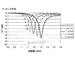
 first feeding element 10 is fed / excited by the feeding point 11, but the second feeding element 20 may be fed / excited by the feeding point 21. Also in this case, due to the symmetry of the structure, the resonance current formed by another coupling path functions as a cancel current in the first feeding element 10 and the isolation characteristics can be improved.

<S11,S21特性>
図5Aは、シミュレーション上で得られたアンテナ装置1のS11特性である。なお、S11特性とは、高周波電子部品等の特性の一種であり、本明細書においては周波数に対する反射損失(リターンロス)で表したマッチング特性とする。具体的に、図5Aは、図1のアンテナ装置1の構成において、給電素子10の給電点側端部16とグランドプレーン70の外縁部71との間の給電点11でギャップ給電したときのS11特性についての計算結果である。なお、設計周波数は、1.35GHzである。
<S11, S21 characteristics>
FIG. 5A shows the S11 characteristic of the antenna device 1 obtained in the simulation. The S11 characteristic is a kind of characteristic of a high-frequency electronic component or the like, and is a matching characteristic represented by a reflection loss (return loss) with respect to a frequency in this specification. Specifically, FIG. 5A shows the S11 when gap feeding is performed at the feeding point 11 between the feeding point side end portion 16 of the feeding element 10 and the outer edge portion 71 of the ground plane 70 in the configuration of the antenna device 1 of FIG. It is the calculation result about a characteristic. The design frequency is 1.35 GHz.

図5Bは、シミュレーション上で得られたアイソレーション特性S21を示す。なお、図5A及び図5Bを解析したときのシミュレーション条件の図1〜図3Cに示す各部の寸法は、単位をmmとすると、
給電素子及び放射素子とグランドプレーンとの最短距離 L13:5
先端部の長さ L12:18
第2の平行部の長さ L34:40
第2の平行部とグランドプレーンの距離 L37:10
給電素子の導体幅 W10:0.5
放射素子の導体幅 W30:0.5
給電素子の厚み T10:0.018
放射素子の厚み T30:0.018
基板及びグランドプレーンのY方向長さ L81:120
基板のX方向長さ L82:150
グランドプレーンのY方向長さ L71:70
給電素子10と20の距離 L83:7
グランドプレーンの厚み T70:0.0018
基板の厚み T80,T90:0.8
である。誘電体である基板80,90の比誘電率は3.3、tanδ=0.003である。なお、給電素子20は給電素子10と対称であって同じ寸法であり、放射素子40は放射素子30と対称であって同じ寸法であるとする。
FIG. 5B shows the isolation characteristic S21 obtained in the simulation. In addition, the dimension of each part shown to FIGS. 1-3C of the simulation conditions when FIG. 5A and FIG. 5B are analyzed, when a unit is mm,
The shortest distance between the feed element and the radiation element and the ground plane L13: 5
Tip length L12: 18
Length of second parallel portion L34: 40
Distance between second parallel portion and ground plane L37: 10
Conductor width of feeding element W10: 0.5
Conductor width of radiation element W30: 0.5
Thickness of feeding element T10: 0.018
Radiation element thickness T30: 0.018
Y direction length of substrate and ground plane L81: 120
The length of the substrate in the X direction L82: 150
Length of ground plane in Y direction L71: 70
Distance between feeding elements 10 and 20 L83: 7
Thickness of ground plane T70: 0.0018
Substrate thickness T80, T90: 0.8
It is. The relative permittivity of the substrates 80 and 90, which are dielectrics, is 3.3 and tan δ = 0.003. The feeding element 20 is symmetric with the feeding element 10 and has the same dimensions, and the radiating element 40 is symmetric with the radiating element 30 and has the same dimensions.

図5Aにおいて、マッチング特性でS11が最小値になるところがインピーダンス整合のとれる、インピーダンス整合周波数であり、この値を動作周波数とする。また、図5Bにおいて、S21の値が局所的に低下し、最小となるところが、アイソレーション極小周波数であって、この周波数で高いアイソレーションが取れる。   In FIG. 5A, the impedance matching frequency at which the impedance matching can be obtained at the point where S11 becomes the minimum value in the matching characteristics, and this value is set as the operating frequency. In FIG. 5B, the value where S21 locally decreases and becomes the minimum is the minimum frequency of isolation, and high isolation can be obtained at this frequency.

本発明の構成では、図4に示すように、第2の給電素子でキャンセル電流が発生することで、動作周波数付近のアイソレーションが向上している。従って、図5Aでの最小値である動作周波数付近で、図5Bで示すアイソレーション周波数S21もほぼ極小値となる。即ち、インピーダンス整合周波数と、アイソレーション極小周波数とが略一致する。   In the configuration of the present invention, as shown in FIG. 4, the cancellation current is generated in the second feeding element, so that the isolation near the operating frequency is improved. Therefore, the isolation frequency S21 shown in FIG. 5B is also a local minimum near the operating frequency that is the minimum value in FIG. 5A. That is, the impedance matching frequency and the isolation minimum frequency substantially coincide.

<第2実施形態>
上述のようなアンテナは搭載される端末(無線装置)の周囲の環境の影響により、アンテナ特性が変動するおそれがある。特に、搭載された端末の位置移動により、周囲の遮蔽物の環境が変化し、アンテナ特性がずれた場合は、そのずれた分を補正するためのチューニングが可能になるように、インピーダンス可変手段をさらに備えてもよい。
Second Embodiment
The antenna characteristics as described above may fluctuate due to the environment around the terminal (wireless device) on which the antenna is mounted. In particular, if the environment of the surrounding shielding object changes due to the movement of the installed terminal and the antenna characteristics deviate, the impedance variable means should be adjusted so that tuning to correct the deviation is possible. Further, it may be provided.

本実施形態において、インピーダンス可変手段を設けることにより、段階的なチューニングが可能となる。   In the present embodiment, stepwise tuning is possible by providing impedance varying means.

図6Aは、本発明の第2実施形態に係るアンテナ装置2の動作を解析するためのコンピュータ上のシミュレーションモデルを示した斜視図である。電磁界シミュレータとして、Microwave Studio(登録商標)(CST社)を使用した。   FIG. 6A is a perspective view showing a simulation model on a computer for analyzing the operation of the antenna device 2 according to the second embodiment of the present invention. Microwave Studio (registered trademark) (CST) was used as an electromagnetic field simulator.

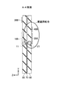
アンテナ装置2は、無線装置(無線通信装置)100の筐体50へ実装させてもよい。図6Bは、無線装置100の平面図であって、給電素子10,20及び放射素子30,40、並びにグランドプレーン70等のアンテナ装置2の構成要素の配置位置を見やすくするため、透視的に示した図である。   The antenna device 2 may be mounted on the housing 50 of the wireless device (wireless communication device) 100. FIG. 6B is a plan view of the wireless device 100 and is shown in a perspective view so as to make it easy to see the arrangement positions of the components of the antenna device 2 such as the feeding elements 10 and 20 and the radiating elements 30 and 40 and the ground plane 70. It is a figure.

無線装置100は、人が携帯可能な無線装置である。無線装置100の具体例として、情報端末機、携帯電話、スマートフォン、パソコン、ゲーム機、テレビ、音楽や映像のプレーヤーなどの電子機器が挙げられる。なお、他の実施形態のアンテナ装置も、無線装置へ実装させてもよい。   The wireless device 100 is a wireless device that can be carried by a person. Specific examples of the wireless device 100 include electronic devices such as an information terminal, a mobile phone, a smartphone, a personal computer, a game machine, a television, and a music and video player. Note that the antenna device according to another embodiment may be mounted on a wireless device.

本実施形態のアンテナ装置2と、図1のアンテナ装置1との違いは、本実施形態では、放射素子30,40にインピーダンス可変手段300,400をさらに設けたことである。インピーダンス可変手段300,400としては、例えばインダクタやキャパシタ、可変容量ダイオードである。インピーダンス可変手段は、スイッチのオンオフにより2値的に切り替えてもよいし、インピーダンスを連続的に変化させてもよい。   The difference between the antenna device 2 of the present embodiment and the antenna device 1 of FIG. 1 is that, in the present embodiment, the radiating elements 30 and 40 are further provided with impedance varying means 300 and 400. The impedance variable means 300, 400 is, for example, an inductor, a capacitor, or a variable capacitance diode. The impedance variable means may be switched in a binary manner by turning on and off the switch, or may continuously change the impedance.

このように設けられたインピーダンス可変手段300、400は、アンテナ装置2へ入力された外部信号によりインピーダンス値を直接制御する。或いは、アンテナ装置2は、例えば、インピーダンス可変手段300,400を制御することにより放射素子30及び放射素子40の基本モードの共振周波数を調整するマッチング回路を備え、結合状態を変化させることに連動して、共振周波数を調整してもよい。   The impedance variable means 300 and 400 provided in this way directly control the impedance value by an external signal input to the antenna device 2. Alternatively, the antenna device 2 includes, for example, a matching circuit that adjusts the resonance frequency of the fundamental mode of the radiating element 30 and the radiating element 40 by controlling the impedance variable means 300 and 400, and interlocks with changing the coupling state. Then, the resonance frequency may be adjusted.

図7A,7Bは、図6Aのようにインピーダンス可変手段300,400を設けることにより、段階的なチューニングを行ったS11特性図である。   7A and 7B are S11 characteristic diagrams in which stepwise tuning is performed by providing impedance variable means 300 and 400 as shown in FIG. 6A.

一例として図6Aのように放射素子30,40に直列に挿入されたインピーダンス可変手段300,400のインダクタ値を変化させてシミュレーションを行ったグラフを示す。図7A,7Bの寸法測定条件は、図5A,図5Bの条件に加えて、インピーダンス可変手段300,400を設置する位置は、単位をmmとして、
端部から可変インダクタまでの距離 L300,L400:29.5
である。
As an example, as shown in FIG. 6A, a graph is shown in which simulation is performed by changing the inductor values of the impedance variable means 300 and 400 inserted in series with the radiating elements 30 and 40. 7A and 7B, in addition to the conditions of FIG. 5A and FIG. 5B, the position where the impedance variable means 300 and 400 are installed is in units of mm.
Distance from end to variable inductor L300, L400: 29.5
It is.

図7のシミュレーションでは、インピーダンス可変手段のインダクタを変化させた。   In the simulation of FIG. 7, the inductor of the impedance variable means is changed.

本実施形態においても、上述の実施形態同様に、図4のように、第2の給電素子20において、意図的に作成した別のカップリング経路により、打ち消しあう電流(キャンセル電流)を発生させることで、電流値を低下させている。従って、アンテナ全体のアイソレーションが高められる。従って、追加の無給電素子を配置しなくても、アンテナ全体のアイソレーションが高められる。即ち、給電素子でキャンセル電流が発生することで、動作周波数付近のアイソレーションが向上している。   Also in the present embodiment, as in the above-described embodiment, as shown in FIG. 4, the second feeding element 20 generates a current (cancellation current) that cancels out by another coupling path that is intentionally created. Thus, the current value is reduced. Therefore, the isolation of the whole antenna is increased. Therefore, the isolation of the entire antenna can be improved without arranging an additional parasitic element. That is, the cancellation current is generated in the feed element, so that the isolation near the operating frequency is improved.

さらに、本実施形態において、インピーダンス可変手段によりインダクタ値を制御することで、インピーダンス整合周波数を制御するときも、同様のキャンセル電流が発生するので、アイソレーション極小周波数も制御することができる。従って、S11が最小値である動作周波数付近で、それぞれのインダクタ値に対して、対応するS21も極小値となる。即ち、インピーダンス整合周波数と、アイソレーション極小周波数とが略一致する。なお、アイソレーション極小周波数は周囲と比べて比較的小さい値になっている箇所で、値の大小による差はここでは考慮しない。   Furthermore, in the present embodiment, by controlling the inductor value by the impedance variable means, the same cancellation current is generated when the impedance matching frequency is controlled, so that the isolation minimum frequency can also be controlled. Therefore, S21 corresponding to each inductor value is also a minimum value in the vicinity of the operating frequency where S11 is the minimum value. That is, the impedance matching frequency and the isolation minimum frequency substantially coincide. Note that the isolation minimum frequency is a relatively small value compared to the surroundings, and the difference due to the magnitude of the value is not considered here.

また、インピーダンス可変手段により、インピーダンス整合周波数とアイソレーション極小周波数の両方を制御する。図7A及び図7Bのグラフからわかるように、インピーダンス整合周波数(動作周波数)を調整して変化させた場合であっても、給電素子でキャンセル電流が発生することで、動作周波数付近のアイソレーションが向上しているので、インピーダンス整合周波数とアイソレーション極小周波数が略一致する。   Further, both the impedance matching frequency and the isolation minimum frequency are controlled by the impedance variable means. As can be seen from the graphs of FIGS. 7A and 7B, even when the impedance matching frequency (operating frequency) is adjusted and changed, the cancellation current is generated in the feed element, so that the isolation near the operating frequency is achieved. Since the impedance is improved, the impedance matching frequency and the isolation minimum frequency substantially coincide with each other.

よって、図7Bでは、インピーダンス可変手段によりインピーダンス整合周波数を変化するにつれて(図7A参照)、アイソレーション極小周波数も略一致して変化するように制御されている。   Therefore, in FIG. 7B, as the impedance matching frequency is changed by the impedance variable means (see FIG. 7A), the isolation minimum frequency is controlled so as to change substantially coincident.

従って、インピーダンス整合周波数とアイソレーション極小周波数を、多段階的なチューニングが可能となる。このような周波数の制御を用いることで、周波数特性を変えることが可能になり、変化する端末の周辺機器の環境へ対応することができる。   Therefore, the impedance matching frequency and the isolation minimum frequency can be tuned in multiple steps. By using such frequency control, it is possible to change the frequency characteristics and cope with the changing environment of the peripheral device of the terminal.

<第3実施形態>
上述の第1実施形態及び第2実施形態では、給電素子と放射素子はYZ方向で重なるように配置されていた。しかし、本発明は、図4に示すようキャンセル電流を発生させる構成例は、この構成に限られず、別の構成であってもよい。
<Third Embodiment>
In the first embodiment and the second embodiment described above, the feeding element and the radiating element are arranged to overlap in the YZ direction. However, in the present invention, the configuration example for generating the cancel current as shown in FIG. 4 is not limited to this configuration, and may be another configuration.

図8は、本発明の第3実施形態であるアンテナ装置3の動作を解析するためのコンピュータ上のシミュレーションモデルを示した斜視図である。図9A〜9Cは、図8のアンテナのYZ方向断面図である。   FIG. 8 is a perspective view showing a simulation model on a computer for analyzing the operation of the antenna device 3 according to the third embodiment of the present invention. 9A to 9C are cross-sectional views in the YZ direction of the antenna of FIG.

本実施形態では、給電素子と放射素子はZ方向で同じ位置には配置されていない点を除いて、上述の実施形態と同様の構成を有る。本実施形態では、A−A’断面では図9Aに示すように、第2の給電素子20Aと第2の放射素子40Aは、Z方向で少しずれた位置で電磁界結合する。同様に、C−C’断面では図9Cに示すように、第1の給電素子10Aと第1の放射素子30Aは、Z方向で少しずれた位置で電磁界結合する。   In the present embodiment, the feeding element and the radiating element have the same configuration as that of the above-described embodiment except that the feeding element and the radiating element are not arranged at the same position in the Z direction. In this embodiment, as shown in FIG. 9A in the A-A ′ cross section, the second feeding element 20 </ b> A and the second radiating element 40 </ b> A are electromagnetically coupled at a position slightly shifted in the Z direction. Similarly, in the C-C ′ cross section, as shown in FIG. 9C, the first feeding element 10 </ b> A and the first radiating element 30 </ b> A are electromagnetically coupled at a position slightly shifted in the Z direction.

このような構成でも、第1の放射素子10Aの放射部は、第2の給電素子20Aの近傍であって第2の給電素子20Aよりもグランドプレーン70から離れた位置で延伸する部分を含んでいる。さらに、第1の放射素子30Aの第2の給電素子20A近傍に延伸する部分は、第2の給電素子20Aが配置されていない部分に、電磁界結合する部分と反対側にグランドプレーン70の外縁部71に沿って延伸している。   Even in such a configuration, the radiating portion of the first radiating element 10A includes a portion extending in the vicinity of the second feeding element 20A and at a position farther from the ground plane 70 than the second feeding element 20A. Yes. Further, the portion of the first radiating element 30A that extends in the vicinity of the second feeding element 20A is the outer edge of the ground plane 70 on the side opposite to the portion that is electromagnetically coupled to the portion where the second feeding element 20A is not disposed. It extends along the portion 71.

第1の放射素子30Aの前記延伸部分と、励起する第1の給電素子10Aの電磁界により、図4に示すように、第2の給電素子20において、意図的に作成した別のカップリング経路により、打ち消しあう電流(キャンセル電流)を発生させることで、電流値を低下させている。従って、追加の無給電素子を配置しなくても、給電素子でキャンセル電流が発生することで、動作周波数付近のアイソレーションが向上し、インピーダンス整合周波数とアイソレーション極小周波数が略一致する。   As shown in FIG. 4, another coupling path intentionally created in the second feeding element 20 by the extended portion of the first radiating element 30A and the electromagnetic field of the first feeding element 10A to be excited. Thus, a current value is reduced by generating a canceling current (cancellation current). Therefore, even if an additional parasitic element is not disposed, a cancellation current is generated in the feeding element, so that isolation near the operating frequency is improved, and the impedance matching frequency and the isolation minimum frequency are substantially matched.

<第4実施形態>
図10は、本発明の第4実施形態であるアンテナ装置4の動作を解析するためのコンピュータ上のシミュレーションモデルを示した斜視図である。図11A〜11Cは、図10のアンテナのZ方向断面図である。
<Fourth embodiment>
FIG. 10 is a perspective view showing a simulation model on a computer for analyzing the operation of the antenna device 4 according to the fourth embodiment of the present invention. 11A to 11C are sectional views in the Z direction of the antenna of FIG.

本実施形態では、第1の給電素子10Bと第1の放射素子30Bが同じ基板に配置され、第2の給電素子20Bと第2の放射素子40Bが同じ基板に配置される。基板以外の寸法は、図1の構成と同様であるため、説明を割愛する。   In the present embodiment, the first feeding element 10B and the first radiating element 30B are arranged on the same substrate, and the second feeding element 20B and the second radiating element 40B are arranged on the same substrate. Since dimensions other than the substrate are the same as those in the configuration of FIG. 1, the description thereof is omitted.

本実施形態では、A−A’断面では図11Aに示すように、第2の給電素子20Bと第2の放射素子40Bは、同じ基板上であって、所定の距離X方向に離れた位置で電磁界結合する。同様に、C−C’断面では図11Cに示すように、第1の給電素子10Bと第1の放射素子30Bは、同じ基板上であって、X方向に離れた位置で電磁界結合する。   In this embodiment, as shown in FIG. 11A in the AA ′ cross section, the second feeding element 20B and the second radiating element 40B are on the same substrate and at a position separated in the predetermined distance X direction. Electromagnetic coupling. Similarly, in the C-C ′ cross section, as shown in FIG. 11C, the first feeding element 10 </ b> B and the first radiating element 30 </ b> B are electromagnetically coupled at positions separated from each other in the X direction on the same substrate.

このような構成でも、第1の放射素子30Bの放射部は、第2の給電素子20Bの近傍であって第2の給電素子20Bよりもグランドプレーン70から離れた位置で延伸する部分を含んでいる。さらに、第1の放射素子30Bの第2の給電素子20B近傍に延伸する部分は、第2の給電素子20Bが配置されていない部分に、電磁界結合する部分と反対側にグランドプレーン70の外縁部71に沿って延伸している。   Even in such a configuration, the radiating portion of the first radiating element 30B includes a portion extending in the vicinity of the second feeding element 20B and at a position farther from the ground plane 70 than the second feeding element 20B. Yes. Further, the portion of the first radiating element 30B extending in the vicinity of the second feeding element 20B is located on the outer edge of the ground plane 70 on the opposite side of the portion where the second feeding element 20B is not disposed to the portion where electromagnetic coupling is performed. It extends along the portion 71.

第1の放射素子30Bの前記延伸部分と、励起する第1の給電素子10Aの電磁界により、図4に示すように、第2の給電素子20において、意図的に作成した別のカップリング経路により、打ち消しあう電流(キャンセル電流)を発生させることで、電流値を低下させている。従って、追加の無給電素子を配置しなくても、給電素子でキャンセル電流が発生することで、動作周波数付近のアイソレーションが向上し、インピーダンス整合周波数とアイソレーション極小周波数が略一致する。   As shown in FIG. 4, another coupling path intentionally created in the second feeding element 20 by the extended portion of the first radiating element 30B and the electromagnetic field of the first feeding element 10A to be excited. Thus, a current value is reduced by generating a canceling current (cancellation current). Therefore, even if an additional parasitic element is not disposed, a cancellation current is generated in the feeding element, so that isolation near the operating frequency is improved, and the impedance matching frequency and the isolation minimum frequency are substantially matched.

上述の第1実施形態〜第4実施形態では、第1、第2の給電素子と放射素子は、最近接箇所は、平行に交差していた。しかし、電磁界結合する部分は、平行でなくてもよい。
給電素子10,20と放射素子30,40との交差角度が異なるアンテナ装置の実施形態バリエーションであってもよい。給電素子10,20と放射素子30,40は、どのような角度で交わっていても、両素子が電磁界結合していれば、放射素子30,40の動作利得は所望の値を確保できる。また、交差角度を変化させても、放射素子30,40の動作利得の特性には、ほとんど影響しない。
In the first to fourth embodiments described above, the first and second feeding elements and the radiating element intersect at the closest point in parallel. However, the portion to be electromagnetically coupled may not be parallel.
It may be a variation of the embodiment of the antenna device in which the crossing angle between the feeding elements 10 and 20 and the radiating elements 30 and 40 is different. Regardless of the angle at which the feeding elements 10 and 20 and the radiating elements 30 and 40 intersect, as long as both elements are electromagnetically coupled, the operation gain of the radiating elements 30 and 40 can ensure a desired value. Further, even if the crossing angle is changed, the operating gain characteristics of the radiating elements 30 and 40 are hardly affected.

なお、キャンセル電流を発生させるためには、例えば、第4実施形態のように第1の給電素子10Bと第1の放射素子30B、第2の給電素子20Bと第2の放射素子40Bが同じ基板に配置される構成例では、給電素子と放射素子が水平方向において近接するが、接触・交差させないように配置し、短絡させないようにする。   In order to generate a cancel current, for example, the first feeding element 10B and the first radiating element 30B, and the second feeding element 20B and the second radiating element 40B are formed on the same substrate as in the fourth embodiment. In the configuration example arranged in (1), the feeding element and the radiating element are close to each other in the horizontal direction, but they are arranged so as not to contact and cross each other and to prevent short circuit.

上述の実施形態では、放射素子は2つ配置されていた。しかし、本発明において、図4に示すようなキャンセル電流を発生させる構成例は、この構成に限られず、別の構成であってもよい。例えば、放射素子が1つであってもよい。   In the above-described embodiment, two radiating elements are arranged. However, in the present invention, the configuration example for generating the cancel current as shown in FIG. 4 is not limited to this configuration, and may be another configuration. For example, there may be one radiating element.

以上、アンテナを複数の実施形態により説明したが、本発明は上記実施形態に限定されるものではない。他の実施形態の一部又は全部との組み合わせや置換などの種々の変形及び改良が、本発明の範囲内で可能である。なお、各図面が示す部材の大きさや位置関係等は、説明を明確にするため誇張していることがある。   As mentioned above, although the antenna was demonstrated by several embodiment, this invention is not limited to the said embodiment. Various modifications and improvements such as combinations and substitutions with some or all of the other embodiments are possible within the scope of the present invention. Note that the size, positional relationship, and the like of the members shown in each drawing may be exaggerated for clarity of explanation.

例えば、アンテナは、図示の形態に限られない。例えば、アンテナは、放射素子に直接又は接続導体を介して間接的に接続された導体部分を有するものでもよいし、放射素子に高周波的(例えば、容量的)に結合された導体部分を有するものでもよい。   For example, the antenna is not limited to the illustrated form. For example, the antenna may have a conductor portion that is directly or indirectly connected to the radiating element via a connecting conductor, or has a conductor portion that is coupled to the radiating element in a high-frequency manner (for example, capacitively). But you can.

また、給電素子、放射素子は、直線的に延びる線状導体に限らず、曲がった導体部分を含むものでもよい。例えば、L字状の導体部分を含むものでもよいし、メアンダ形状の導体部分を含むものでもよいし、途中で分岐した導体部分を含むものでもよい。   Further, the feeding element and the radiating element are not limited to linear conductors extending linearly, but may include a bent conductor portion. For example, an L-shaped conductor portion may be included, a meander-shaped conductor portion may be included, or a conductor portion branched in the middle may be included.

また、グランドプレーンを有する伝送線路は、マイクロストリップラインに限られない。例えば、ストリップライン、グランドプレーン付きコプレーナウェーブガイド(導体面とは反対側の表面にグランドプレーンが配置されたコプレーナウェーブガイド)などが挙げられる。   Further, the transmission line having the ground plane is not limited to the microstrip line. For example, a stripline, a coplanar waveguide with a ground plane (a coplanar waveguide having a ground plane disposed on the surface opposite to the conductor surface), and the like can be given.

また、グランドプレーンは、図示の外形形状に限られず、他の外形形状を有する導体パターンでもよい。また、グランドプレーンは、平面状に形成された形態に限られず、曲面状に形成された形態でもよい。同様に、板状導体は、図示の外形形状に限られず、他の外形形状を有する導体でもよい。また、板状導体は、平面状に形成された形態に限られず、曲面状に形成された形態でもよい。   The ground plane is not limited to the illustrated outer shape, and may be a conductor pattern having another outer shape. Further, the ground plane is not limited to a planar shape, and may be a curved surface. Similarly, the plate conductor is not limited to the illustrated outer shape, and may be a conductor having another outer shape. Further, the plate-like conductor is not limited to a flat shape, and may be a curved shape.

また、「板状」には、「箔状」又は「フィルム状」の意味が含まれてよい。   Further, the “plate shape” may include the meaning of “foil shape” or “film shape”.

以上、マルチアンテナを実施形態及び実施例により説明したが、本発明は上記実施形態及び実施例に限定されるものではない。他の実施形態及び実施例の一部又は全部との組み合わせや置換などの種々の変形及び改良が、本発明の範囲内で可能である。   As described above, the multi-antenna has been described based on the embodiments and examples, but the present invention is not limited to the above-described embodiments and examples. Various modifications and improvements such as combinations and substitutions with part or all of other embodiments and examples are possible within the scope of the present invention.

本出願は、2014年5月30日に日本国特許庁に出願された特願2014−113074号に基づく優先権を主張するものであり、特願2014−113074号の全内容を本出願に援用する。   This application claims priority based on Japanese Patent Application No. 2014-1113074 filed with the Japan Patent Office on May 30, 2014, and the entire contents of Japanese Patent Application No. 2014-1113074 are incorporated in this application. To do.

1,2,3,4 アンテナ装置(マルチアンテナ)
10,20,10A,20A,10B,20B 給電素子
11,21 給電点
12,22 先端部(給電素子)
13,23 給電点接続部(給電素子)
14,24 折れ曲がり部(給電素子)
15,25 端部(給電素子)
16,26 給電点側端部(給電素子)
30,40,30A,40A,30B,40B 放射素子
31,41 端部(放射素子)
32,42 第1の平行部(放射素子)
33,43 傾斜部(放射素子)
34,44 第2の平行部(放射素子)
35,36,45,46 折れ曲がり部(放射素子)
37,47 端部
38,48 中央部(放射素子)
39,49 延伸部(放射素子)
50 給電部(放射素子30)
60 給電部(放射素子40)
70 グランドプレーン
71 外縁部(縁部)
80,90 基板
84,94 ストリップ導体
85 スイッチ素子
86 給電回路
100 無線装置
300,400 インピーダンス可変手段

1,2,3,4 antenna device (multi-antenna)
10, 20, 10A, 20A, 10B, 20B Feeding elements 11, 21 Feeding points 12, 22 Tip (feeding element)
13, 23 Feed point connection (feed element)
14, 24 Bent part (feeding element)
15, 25 End (feeding element)
16, 26 Feed point side end (feed element)
30, 40, 30A, 40A, 30B, 40B Radiating element 31, 41 End (radiating element)
32, 42 First parallel part (radiating element)
33,43 Inclined part (radiating element)
34, 44 Second parallel part (radiating element)
35, 36, 45, 46 Bent part (radiating element)
37, 47 Ends 38, 48 Center part (radiating element)
39, 49 Extending part (radiating element)
50 Power feeding unit (radiating element 30)
60 Power feeding unit (radiating element 40)
70 Ground plane 71 Outer edge (edge)
80, 90 Substrate 84, 94 Strip conductor 85 Switch element 86 Feed circuit 100 Radio apparatus 300, 400 Impedance variable means

Claims (15)

グランドプレーンと、
第1の給電点と、
前記第1の給電点とは異なる第2の給電点と、
前記第1の給電点に接続される第1の給電素子と、
前記第2の給電点に接続され、かつ、キャンセル電流が発生する第2の給電素子と、
前記第1の給電素子及び前記第2の給電素子と電磁界結合することにより給電され、放射導体として機能する放射素子とを備え、
前記放射素子は、
前記第1の給電素子と電磁界結合することにより給電され、放射導体として機能する第1の放射素子と、
前記第2の給電素子と電磁界結合することにより給電され、放射導体として機能する第2の放射素子とを備え、
前記第1の放射素子と前記第2の放射素子とが、互いに異なる平面に、前記平面に直交する方向からの平面視において交差するように配置される、
マルチアンテナ。
A ground plane,
A first feeding point;
A second feeding point different from the first feeding point;
A first feeding element connected to the first feeding point;
A second feeding element connected to the second feeding point and generating a canceling current;
It said first feeding element and is powered by the electromagnetic field coupling and the second feeding element, e Bei a radiating element functioning as a radiation conductor,
The radiating element is:
A first radiating element that is fed by electromagnetic coupling with the first feeding element and functions as a radiating conductor;
A second radiating element that is fed by electromagnetic coupling with the second feeding element and functions as a radiating conductor;
The first radiating element and the second radiating element are arranged to intersect with each other in different planes in a plan view from a direction orthogonal to the plane.
Multi antenna.
前記第2の給電点の近傍に延伸し、かつ、前記グランドプレーンの縁部に沿って延伸する部位を有する前記第1の放射素子と、
前記第1の給電点の近傍に延伸し、かつ、前記グランドプレーンの縁部に沿って延伸する部位を有する前記第2の放射素子とを備える、請求項に記載のマルチアンテナ。
The first radiating element extending in the vicinity of the second feeding point and having a portion extending along an edge of the ground plane;
2. The multi-antenna according to claim 1 , further comprising: the second radiating element that extends in the vicinity of the first feeding point and has a portion that extends along an edge of the ground plane.
前記第1の給電素子及び前記第2の給電素子の共振の基本モードを与える電気長をLe10,Le20、前記第1の放射素子及び前記第2の放射素子の共振の基本モードを与える電気長をLe30,Le40、前記放射素子の基本モードの共振周波数における前記第1の給電素子、前記第2の給電素子、前記第1の放射素子、または前記第2の放射素子上での波長をλとして、Le10,Le20が、(3/8)・λ以下であり、かつ、Le30,Le40が、(3/8)・λ以上(5/8)・λ以下である、請求項1または2に記載のマルチアンテナ。 The electrical length giving the fundamental mode of resonance of the first feeding element and the second feeding element is Le10, Le20, and the electrical length giving the fundamental mode of resonance of the first radiating element and the second radiating element is Le30, Le40, the wavelength on the first feeding element , the second feeding element, the first radiating element, or the second radiating element at the resonance frequency of the fundamental mode of the radiating element as λ , LE 10, LE20 is, is at (3/8) · lambda less and, Le30, Le40 is, (3/8) is · lambda or (5/8) · lambda less, according to claim 1 or 2 Multi-antenna. インピーダンス可変手段を有し、前記インピーダンス可変手段により、アイソレーション極小周波数を制御する、請求項1から3のいずれか一項に記載のマルチアンテナ。 The multi-antenna according to any one of claims 1 to 3 , further comprising an impedance variable unit, wherein the minimum impedance frequency is controlled by the impedance variable unit. 前記インピーダンス可変手段により、インピーダンス整合周波数と前記アイソレーション極小周波数とを制御する、請求項記載のマルチアンテナ。 5. The multi-antenna according to claim 4 , wherein the impedance variable means controls the impedance matching frequency and the minimum isolation frequency. 前記インピーダンス整合周波数と、前記アイソレーション極小周波数とが略一致する、請求項記載のマルチアンテナ。 The multi-antenna according to claim 5 , wherein the impedance matching frequency and the isolation minimum frequency substantially coincide with each other. 給電回路と、前記第1の給電点と前記第2の給電点と前記給電回路とに接続されたスイッチ素子とを備え、
前記第1の給電素子への給電と、前記第2の給電素子への給電とを、相補的に切り替え可能である、請求項1からのいずれか一項記載のマルチアンテナ。
A power feeding circuit; and a switch element connected to the first power feeding point, the second power feeding point, and the power feeding circuit,
The multi-antenna according to any one of claims 1 to 6 , wherein the power feeding to the first power feeding element and the power feeding to the second power feeding element can be switched complementarily.
前記第1の放射素子及び前記第2の放射素子の基本モードの共振周波数における真空中の波長をλとする場合、前記第1の給電素子と前記第1の放射素子との最短距離、及び前記第2の給電素子と前記第2の放射素子との最短距離が0.2×λ以下である、請求項1から7のいずれか一項に記載のマルチアンテナ。 If the wavelength in vacuum at the resonant frequency of the fundamental mode of the first radiating element and said second radiating element and the lambda 0, the shortest distance between the first feed element and the first radiation element, and the second shortest distance between the feed element and the second radiating element is 0.2 × lambda 0 or less, the multi-antenna according to any one of claims 1 to 7. 前記第1の放射素子は前記第1の給電素子から給電を受ける給電部を有し、前記第2の放射素子は前記第2の給電素子から給電を受ける給電部を有し、前記給電部は、前記第1の放射素子、前記第2の放射素子のそれぞれの基本モードの共振周波数における最も低いインピーダンスになる部分以外に位置する、請求項1からのいずれか一項に記載のマルチアンテナ。 Wherein the first radiating element has a feeding portion for receiving power from said first feed element, the second radiating element has a feeding portion for receiving power from the second feed element, each power supply unit The multi-antenna according to any one of claims 1 to 8 , wherein the multi-antenna is located in a portion other than a portion having the lowest impedance at a resonance frequency of each fundamental mode of the first radiating element and the second radiating element. . 前記第1の放射素子は前記第1の給電素子から給電を受ける給電部を有し、前記第2の放射素子は前記第2の給電素子から給電を受ける給電部を有し、前記給電部は、前記第1の放射素子、前記第2の放射素子のそれぞれの基本モードの共振周波数における最も低いインピーダンスになる部分から、前記第1の放射素子、前記第2の放射素子のそれぞれの全長の1/8以上の距離を離した部位に位置する、請求項1からのいずれか一項に記載のマルチアンテナ。 Wherein the first radiating element has a feeding portion for receiving power from said first feed element, the second radiating element has a feeding portion for receiving power from the second feed element, each power supply unit , said first radiating element, from the lowest becomes impedance portion at the resonance frequency of the respective fundamental mode of the second radiating element, wherein the first radiating element, each of the total length of the second radiating element The multi-antenna as described in any one of Claim 1 to 9 located in the site | part which separated the distance of 1/8 or more. 前記第1の給電素子と前記第1の放射素子とが最短距離で並走する距離、及び前記第2の給電素子と前記第2の放射素子とが最短距離で並走する距離は、前記第1の放射素子、前記第2の放射素子のそれぞれの長さの3/8以下である、請求項1から10のいずれか一項に記載のマルチアンテナ。 Wherein the first feeding element distance first and radiating elements run in parallel with the shortest distance, and the distance of said second feed element and the second radiating element is running parallel with the shortest distance, the first The multi-antenna according to any one of claims 1 to 10 , wherein the length of each of the first radiating element and the second radiating element is 3/8 or less. 前記第1の放射素子は前記第1の給電素子から給電を受ける給電部を有し、前記第2の放射素子は前記第2の給電素子から給電を受ける給電部を有し、前記第1の放射素子、前記第2の放射素子のそれぞれの基本モードの共振周波数における真空中の波長をλとする場合、前記給電部と、前記第1の給電点、前記第2の給電点のそれぞれのグランド基準であるグランドプレーンとの最短距離は、0.0034λ以上0.21λ以下である、請求項1から11のいずれか一項に記載のマルチアンテナ。 The first radiating element includes a power feeding unit that receives power from the first power feeding element , and the second radiating element includes a power feeding unit that receives power from the second power feeding element , When the wavelength in vacuum at the resonance frequency of the fundamental mode of each of the radiating element and the second radiating element is λ 0 , each of the feeding units, the first feeding point , and the second feeding point shortest distance, 0.0034Ramuda is 0 or more 0.21Ramuda 0 or less, the multi-antenna according to any one of claims 1 to 11 with the ground plane is the ground reference. グランドプレーンと、
第1の給電点と、
前記第1の給電点とは異なる第2の給電点と、
前記第1の給電点に接続される第1の給電素子と、
前記第2の給電点に接続され、かつ、キャンセル電流が発生する第2の給電素子と、
前記第1の給電素子及び前記第2の給電素子から給電される放射素子と、を備え、
前記放射素子は、
前記第1の給電素子と電磁界結合することにより給電され、放射導体として機能する第1の放射素子と、
前記第2の給電素子と電磁界結合することにより給電され、放射導体として機能する第2の放射素子とを備え、
前記第1の放射素子と前記第2の放射素子とが、互いに異なる平面に、前記平面に直交する方向からの平面視において交差するように配置され、
記第1の給電素子及び前記第2の給電素子が共振することにより放射導体として機能する、マルチアンテナ。
A ground plane,
A first feeding point;
A second feeding point different from the first feeding point;
A first feeding element connected to the first feeding point;
A second feeding element connected to the second feeding point and generating a canceling current;
A radiating element fed from the first feeding element and the second feeding element,
The radiating element is:
A first radiating element that is fed by electromagnetic coupling with the first feeding element and functions as a radiating conductor;
A second radiating element that is fed by electromagnetic coupling with the second feeding element and functions as a radiating conductor;
The first radiating element and the second radiating element are arranged to intersect with each other in different planes in a plan view from a direction orthogonal to the plane,
Before SL first feed element and the second feed element functions as a radiation conductor by resonating, multi-antenna.
前記第1の放射素子は、前記第1の給電素子共振周波数と異なる共振周波数を有し、
前記第2の放射素子は、前記第2の給電素子の共振周波数と異なる共振周波数を有する、請求項13に記載のマルチアンテナ。
The first radiating element has a resonance frequency different from a resonance frequency of the first feeding element;
The multi-antenna according to claim 13 , wherein the second radiating element has a resonance frequency different from a resonance frequency of the second feeding element .
請求項1から14のいずれか一項に記載のマルチアンテナを備える、無線装置。 A wireless device comprising the multi-antenna according to any one of claims 1 to 14 .
JP2016523544A 2014-05-30 2015-05-27 Multi-antenna and radio apparatus including the same Expired - Fee Related JP6465109B2 (en)

Applications Claiming Priority (3)

Application Number Priority Date Filing Date Title
JP2014113074 2014-05-30
PCT/JP2015/065315 WO2015182677A1 (en) 2014-05-30 2015-05-27 Multiple antenna and wireless device provided with same

Publications (2)

Publication Number Publication Date
JPWO2015182677A1 JPWO2015182677A1 (en) 2017-04-20
JP6465109B2 true JP6465109B2 (en) 2019-02-06

Family

ID=54699000

Family Applications (1)

Application Number Title Priority Date Filing Date
JP2016523544A Expired - Fee Related JP6465109B2 (en) 2014-05-30 2015-05-27 Multi-antenna and radio apparatus including the same

Country Status (5)

Country Link
US (1) US10205232B2 (en)
JP (1) JP6465109B2 (en)
CN (1) CN106415929B (en)
TW (1) TWI686009B (en)
WO (1) WO2015182677A1 (en)

Families Citing this family (18)

* Cited by examiner, † Cited by third party
Publication number Priority date Publication date Assignee Title
US10205244B2 (en) 2013-12-19 2019-02-12 Intel IP Corporation Platform independent antenna
US10566689B2 (en) * 2015-09-25 2020-02-18 Apple Inc. Antenna system
US10431891B2 (en) * 2015-12-24 2019-10-01 Intel IP Corporation Antenna arrangement
KR102350154B1 (en) * 2017-06-09 2022-01-11 미쓰비시덴키 가부시키가이샤 printed board
US10615486B2 (en) * 2017-06-28 2020-04-07 Intel IP Corporation Antenna system
CN109309283A (en) * 2017-07-27 2019-02-05 国基电子(上海)有限公司 Antenna assembly
CN108039584B (en) * 2017-12-01 2021-01-08 Oppo广东移动通信有限公司 Antenna assembly and electronic equipment
US11228095B2 (en) * 2018-06-29 2022-01-18 Google Llc Wearable devices with antennas plated on high permittivity housing materials
CN109149071B (en) * 2018-08-20 2021-05-07 瑞声光电科技(常州)有限公司 Antenna module and mobile terminal
JP6678722B1 (en) * 2018-10-31 2020-04-08 京セラ株式会社 Antenna, wireless communication module and wireless communication device
CN110011027A (en) * 2018-12-28 2019-07-12 瑞声科技(新加坡)有限公司 A kind of antenna, aerial array and base station
TWI701599B (en) * 2019-01-29 2020-08-11 國立臺灣大學 Contact switch and system thereof and interactive building block system carrying the contact switch
JP6820068B1 (en) * 2019-07-25 2021-01-27 Necプラットフォームズ株式会社 Wireless device
EP3793030A1 (en) 2019-09-12 2021-03-17 Nokia Solutions and Networks Oy Antenna
US20210111486A1 (en) * 2020-12-21 2021-04-15 Intel Corporation Antenna assembly with isolation network
CN115882200A (en) * 2021-09-26 2023-03-31 中兴通讯股份有限公司 Antenna and electronic device
CN116345122A (en) * 2021-12-22 2023-06-27 荣耀终端有限公司 Foldable electronic device and antenna system thereof
CN116345145A (en) * 2021-12-22 2023-06-27 荣耀终端有限公司 Foldable electronic device and antenna system thereof

Family Cites Families (20)

* Cited by examiner, † Cited by third party
Publication number Priority date Publication date Assignee Title
JP4363936B2 (en) 2002-09-26 2009-11-11 パナソニック株式会社 Antenna for wireless terminal device and wireless terminal device
JP2005057723A (en) 2003-07-18 2005-03-03 Matsushita Electric Ind Co Ltd Antenna module and antenna system
JP4278534B2 (en) * 2004-02-19 2009-06-17 富士通テン株式会社 Circularly polarized antenna, antenna device, and processing device
US20050099335A1 (en) 2003-11-10 2005-05-12 Shyh-Jong Chung Multiple-frequency antenna structure
JP2006042111A (en) * 2004-07-29 2006-02-09 Matsushita Electric Ind Co Ltd Antenna device
JP4257349B2 (en) 2005-09-08 2009-04-22 株式会社カシオ日立モバイルコミュニケーションズ Antenna device and wireless communication terminal
JP4422767B2 (en) 2005-10-06 2010-02-24 パナソニック株式会社 Antenna device for portable terminal and portable terminal
JP2007221344A (en) 2006-02-15 2007-08-30 Toshiba Corp Antenna system, ic loaded with same and portable terminal loaded with antenna system
US7453402B2 (en) * 2006-06-19 2008-11-18 Hong Kong Applied Science And Research Institute Co., Ltd. Miniature balanced antenna with differential feed
JP2008278219A (en) 2007-04-27 2008-11-13 Toshiba Corp Antenna device
JP5532847B2 (en) * 2009-11-20 2014-06-25 船井電機株式会社 Multi-antenna device and portable device
JPWO2011102143A1 (en) * 2010-02-19 2013-06-17 パナソニック株式会社 Antenna device and portable wireless terminal equipped with the same
JP5664322B2 (en) * 2011-02-21 2015-02-04 船井電機株式会社 Multi-antenna device and communication device
US20130082898A1 (en) 2011-04-11 2013-04-04 Kenichi Asanuma Antenna apparatus provided with two antenna elements and sleeve element for use in mobile communications
KR101779457B1 (en) 2011-04-22 2017-09-19 삼성전자주식회사 Antenna device for portable terminal
JP5076019B1 (en) * 2011-10-19 2012-11-21 株式会社東芝 ANTENNA DEVICE AND ELECTRONIC DEVICE HAVING THE ANTENNA DEVICE
TWI511378B (en) * 2012-04-03 2015-12-01 Ind Tech Res Inst Multi-band multi-antenna system and communiction device thereof
JP5631921B2 (en) * 2012-04-17 2014-11-26 太陽誘電株式会社 Multi-antenna and electronic device
WO2014013840A1 (en) * 2012-07-20 2014-01-23 旭硝子株式会社 Antenna device and wireless device provided with same
TWI539660B (en) 2013-05-03 2016-06-21 宏碁股份有限公司 Mobile device

Also Published As

Publication number Publication date
CN106415929B (en) 2019-11-15
TWI686009B (en) 2020-02-21
US10205232B2 (en) 2019-02-12
WO2015182677A1 (en) 2015-12-03
CN106415929A (en) 2017-02-15
US20170077599A1 (en) 2017-03-16
TW201603392A (en) 2016-01-16
JPWO2015182677A1 (en) 2017-04-20

Similar Documents

Publication Publication Date Title
JP6465109B2 (en) Multi-antenna and radio apparatus including the same
US10741929B2 (en) Antenna and wireless communication device
US9905919B2 (en) Antenna, antenna device, and wireless device
TWI600210B (en) Multi-band antenna
JP6614363B2 (en) ANTENNA DEVICE AND ELECTRONIC DEVICE
JP6311833B2 (en) Antenna device
WO2016148274A1 (en) Antenna and wireless communication device
WO2010050278A1 (en) Radio communication device
WO2012124247A1 (en) Antenna device, and wireless communication device
JP2019213241A (en) Antenna device and wireless apparatus
KR20060042232A (en) Reverse f-shaped antenna
WO2014132519A1 (en) Antenna, printed circuit board, and wireless communication device
JP2014053885A (en) Multi-band antenna
JP6229814B2 (en) Communication terminal device
US8797225B2 (en) Antenna device and communication terminal apparatus
JP5900660B2 (en) MIMO antenna and radio apparatus
WO2013145623A1 (en) Antenna unit and mobile wireless device equipped with same
JP6233319B2 (en) Multiband antenna and radio apparatus
WO2014203967A1 (en) Antenna device and wireless device provided therewith
TWI524589B (en) Low impedance slot fed antenna
WO2011099673A1 (en) Internal antenna using a terminal ground

Legal Events

Date Code Title Description
A621 Written request for application examination

Free format text: JAPANESE INTERMEDIATE CODE: A621

Effective date: 20180223

A131 Notification of reasons for refusal

Free format text: JAPANESE INTERMEDIATE CODE: A131

Effective date: 20181002

A521 Request for written amendment filed

Free format text: JAPANESE INTERMEDIATE CODE: A523

Effective date: 20181129

TRDD Decision of grant or rejection written
A01 Written decision to grant a patent or to grant a registration (utility model)

Free format text: JAPANESE INTERMEDIATE CODE: A01

Effective date: 20181211

A61 First payment of annual fees (during grant procedure)

Free format text: JAPANESE INTERMEDIATE CODE: A61

Effective date: 20181224

R150 Certificate of patent or registration of utility model

Ref document number: 6465109

Country of ref document: JP

Free format text: JAPANESE INTERMEDIATE CODE: R150

R250 Receipt of annual fees

Free format text: JAPANESE INTERMEDIATE CODE: R250

LAPS Cancellation because of no payment of annual fees