JP4507563B2 - Multiprocessor system - Google Patents
Multiprocessor system Download PDFInfo
- Publication number
- JP4507563B2 JP4507563B2 JP2003379294A JP2003379294A JP4507563B2 JP 4507563 B2 JP4507563 B2 JP 4507563B2 JP 2003379294 A JP2003379294 A JP 2003379294A JP 2003379294 A JP2003379294 A JP 2003379294A JP 4507563 B2 JP4507563 B2 JP 4507563B2
- Authority
- JP
- Japan
- Prior art keywords
- bus
- cache coherence
- directory
- cache
- processors
- Prior art date
- Legal status (The legal status is an assumption and is not a legal conclusion. Google has not performed a legal analysis and makes no representation as to the accuracy of the status listed.)
- Expired - Fee Related
Links
- 230000015654 memory Effects 0.000 claims description 168
- 230000008859 change Effects 0.000 claims description 15
- 230000005540 biological transmission Effects 0.000 claims description 5
- 230000008878 coupling Effects 0.000 description 29
- 238000010168 coupling process Methods 0.000 description 29
- 238000005859 coupling reaction Methods 0.000 description 29
- 238000005192 partition Methods 0.000 description 14
- 238000000926 separation method Methods 0.000 description 10
- 238000000034 method Methods 0.000 description 7
- 230000004044 response Effects 0.000 description 5
- 238000010586 diagram Methods 0.000 description 4
- 230000010365 information processing Effects 0.000 description 4
- 230000006870 function Effects 0.000 description 3
- 238000001693 membrane extraction with a sorbent interface Methods 0.000 description 3
- 230000000644 propagated effect Effects 0.000 description 3
- 230000009471 action Effects 0.000 description 2
- 230000015556 catabolic process Effects 0.000 description 2
- 238000006731 degradation reaction Methods 0.000 description 2
- 230000006872 improvement Effects 0.000 description 2
- 230000007246 mechanism Effects 0.000 description 2
- 230000007704 transition Effects 0.000 description 2
- 238000005266 casting Methods 0.000 description 1
- 230000006866 deterioration Effects 0.000 description 1
- 238000011982 device technology Methods 0.000 description 1
- 238000005516 engineering process Methods 0.000 description 1
- 238000010977 unit operation Methods 0.000 description 1
Images


Classifications
-
- G—PHYSICS
- G06—COMPUTING; CALCULATING OR COUNTING
- G06F—ELECTRIC DIGITAL DATA PROCESSING
- G06F12/00—Accessing, addressing or allocating within memory systems or architectures
- G06F12/02—Addressing or allocation; Relocation
- G06F12/08—Addressing or allocation; Relocation in hierarchically structured memory systems, e.g. virtual memory systems
- G06F12/0802—Addressing of a memory level in which the access to the desired data or data block requires associative addressing means, e.g. caches
- G06F12/0806—Multiuser, multiprocessor or multiprocessing cache systems
- G06F12/0815—Cache consistency protocols
- G06F12/0817—Cache consistency protocols using directory methods
-
- G—PHYSICS
- G06—COMPUTING; CALCULATING OR COUNTING
- G06F—ELECTRIC DIGITAL DATA PROCESSING
- G06F12/00—Accessing, addressing or allocating within memory systems or architectures
- G06F12/02—Addressing or allocation; Relocation
- G06F12/08—Addressing or allocation; Relocation in hierarchically structured memory systems, e.g. virtual memory systems
- G06F12/0802—Addressing of a memory level in which the access to the desired data or data block requires associative addressing means, e.g. caches
- G06F12/0806—Multiuser, multiprocessor or multiprocessing cache systems
- G06F12/0815—Cache consistency protocols
- G06F12/0831—Cache consistency protocols using a bus scheme, e.g. with bus monitoring or watching means
-
- G—PHYSICS
- G06—COMPUTING; CALCULATING OR COUNTING
- G06F—ELECTRIC DIGITAL DATA PROCESSING
- G06F12/00—Accessing, addressing or allocating within memory systems or architectures
- G06F12/02—Addressing or allocation; Relocation
- G06F12/08—Addressing or allocation; Relocation in hierarchically structured memory systems, e.g. virtual memory systems
- G06F12/0802—Addressing of a memory level in which the access to the desired data or data block requires associative addressing means, e.g. caches
- G06F12/0806—Multiuser, multiprocessor or multiprocessing cache systems
- G06F12/0813—Multiuser, multiprocessor or multiprocessing cache systems with a network or matrix configuration
Landscapes
- Engineering & Computer Science (AREA)
- Theoretical Computer Science (AREA)
- Physics & Mathematics (AREA)
- General Engineering & Computer Science (AREA)
- General Physics & Mathematics (AREA)
- Memory System Of A Hierarchy Structure (AREA)
- Multi Processors (AREA)
Description
本発明は、複数のCPUを持ちCPU間で主記憶を共有する共有メモリ型並列計算機におけるCPU間のキャッシュメモリの一致制御、すなわちCPU間キャッシュコヒーレンス制御方式に属する。 The present invention belongs to a cache memory matching control between CPUs in a shared memory parallel computer having a plurality of CPUs and sharing a main memory among the CPUs, that is, an inter-CPU cache coherence control system.
デバイス技術の進歩により、CPUの動作周波数の向上は急峻であり、これに対しCPUから主記憶をアクセスする際のメモリアクセスレイテンシは、CPUから主記憶までの物理的な距離や主記憶素子の特性に制約されることから、絶対時間での改善は緩やかである。つまりCPUの単位動作時間(=1秒÷動作周波数)を単位として見た場合、アクセスレイテンシ時間はむしろ延びる方向にあり、アクセスレイテンシが性能向上のボトルネックとなる傾向にある。 Due to advances in device technology, the operating frequency of the CPU has been sharply improved. On the other hand, the memory access latency when accessing the main memory from the CPU is the physical distance from the CPU to the main memory and the characteristics of the main memory element. Therefore, the improvement in absolute time is moderate. That is, when the unit operation time (= 1 second ÷ operation frequency) of the CPU is used as a unit, the access latency time tends to be rather extended, and the access latency tends to be a bottleneck for performance improvement.
この相対的なメモリアクセスレイテンシの悪化による性能低下を救う技術がキャッシュメモリである。キャッシュメモリは、高速小容量のバッファをCPUに近いところに用意し、使用頻度の高いデータのコピーを登録することで、実効的なメモリアクセスレイテンシを削減する技術である。 A cache memory is a technique that saves performance degradation due to the deterioration of the relative memory access latency. Cache memory is a technology that reduces effective memory access latency by preparing a high-speed small-capacity buffer near a CPU and registering a copy of frequently used data.
現代の計算機では、前述のキャッシュメモリを実装するCPUを複数個搭載し、CPU全部もしくは一部の間で主記憶を共有する共有メモリ型並列計算機の構成、もしくは共有メモリ型並列計算機のクラスタ構成を採用することが多い。CPUを複数搭載するのは、(1)性能向上、(2)可用性の向上(1つのCPUに障害が発生した場合にもシステムダウンを防ぐ)、を狙うことによる。計算機サービスに使用される「サーバ」と呼ばれる計算機では、最低でも2CPU以上の共有メモリ型並列計算機の構成が必須とされる。 In modern computers, a configuration of a shared memory parallel computer in which a plurality of CPUs on which the above-described cache memory is mounted is mounted and main memory is shared among all or a part of the CPU, or a cluster configuration of a shared memory parallel computer is used. Often adopted. The reason for mounting a plurality of CPUs is to (1) improve performance and (2) improve availability (to prevent system down even when a failure occurs in one CPU). In a computer called a “server” used for a computer service, a configuration of a shared memory parallel computer having at least 2 CPUs is essential.
このように、キャッシュメモリを持った複数のCPUが主記憶を共有する場合、キャッシュメモリの一致制御、いわゆるキャッシュコヒーレンス制御が問題になる。これはあるCPU(A)がキャッシュメモリに登録しているデータを別なCPU(B)がストア命令で更新した場合、その更新結果はCPU(A)のキャッシュメモリに反映される(キャッシュメモリ上のデータが更新される、もしくは無効化される)必要がある。 Thus, when a plurality of CPUs having a cache memory share main memory, cache memory matching control, so-called cache coherence control, becomes a problem. This is because when another CPU (B) updates data registered in a cache memory by a CPU (A) with a store instruction, the update result is reflected in the cache memory of the CPU (A) (on the cache memory). Data needs to be updated or invalidated).
このようなキャッシュメモリ一致制御は、一般的にはバスを通じた制御で行われる。これは、あるプロセッサによるデータの更新はバスを通じて全CPUにブロードキャストされる仕組みと、各CPUがバスを常時チェックしブロードキャストされた更新情報をキャッシュメモリに登録されているデータに反映させる(スヌープ動作)仕組みとにより実現される。 Such cache memory matching control is generally performed by control through a bus. This is because a data update by a processor is broadcast to all CPUs through a bus, and each CPU constantly checks the bus and reflects the broadcast update information in the data registered in the cache memory (snoop operation). Realized by the mechanism.
上記バスによるキャッシュコヒーレンス制御は、バス上でキャッシュコヒーレンスリクエストが輻輳を起こし得ることから、CPU数の多い大規模な共有メモリ型マルチプロセッサ構成を全てバスで実現すると各CPUの性能が低下する問題がある。この問題に対し、メモリ上のデータそれぞれに、どのプロセッサがキャッシュメモリにデータを登録しているかを覚えるディレクトリを設け、ディレクトリに登録された情報に基づき必要なプロセッサにのみキャッシュコヒーレンスリクエストを伝達することにより、バスに比べて輻輳の発生頻度を低下させることが出来る。本方式がいわゆるNUMA(Non-Uniform Memory Architecture)型マルチプロセッサである。NUMA型マルチプロセッサについては、情報処理学会誌情報処理Vol.34 No.1(1993年1月)、96〜105頁「マルチプロセッサの記憶システム(1)」を参考にされたい。 Since the cache coherence control by the bus can cause congestion of cache coherence requests on the bus, if all large-scale shared memory multiprocessor configurations with a large number of CPUs are realized by the bus, the performance of each CPU is degraded. is there. To solve this problem, provide a directory that remembers which processor is registering data in the cache memory for each data on the memory, and transmit a cache coherence request only to the required processor based on the information registered in the directory. Therefore, it is possible to reduce the occurrence frequency of congestion as compared with the bus. This method is a so-called NUMA (Non-Uniform Memory Architecture) type multiprocessor. Regarding the NUMA type multiprocessor, refer to Information Processing Society of Japan Information Processing Vol.34 No.1 (January 1993), pages 96 to 105 “Multiprocessor Storage System (1)”.
NUMA型はCPU間バスのように全てのCPUからのリクエストが集中する箇所がないことから、CPUの増加に従い性能をスケーラブルに高めることが出来るメリットがある。他方、バス型のマルチプロセッサであればリクエストをバスに送出した直後にコヒーレンス制御が低レイテンシで実行されるのに対し、NUMAではリクエストが発生するとこれに対して他CPUに対するコヒーレンス制御を行うか行わないかの判定を行う回路を経て、更にそこからコヒーレンス制御要求が対象CPUに伝達されるという手順を踏むことから、一般にコヒーレンス制御の遅延時間が大きく、小規模システムではバス型マルチプロセッサに性能で劣るというデメリットがある。 The NUMA type has no merit that the requests from all the CPUs are concentrated like the inter-CPU bus, so that the performance can be improved in a scalable manner as the number of CPUs increases. On the other hand, in the case of a bus type multiprocessor, coherence control is executed with low latency immediately after a request is sent to the bus, whereas in NUMA, when a request occurs, whether or not coherence control is performed for other CPUs. The delay time of the coherence control is generally large, and the performance of the bus type multiprocessor is small in a small-scale system because the coherence control request is further transmitted to the target CPU from there. There is a disadvantage that it is inferior.
特開平10−240707号公報では、バス型のマルチプロセッサを単位としてNUMAでこれらを結合したシステムを構築する技術を開示している。更に特開平10−240707では、NUMAシステムをパーティション分割した場合にNUMA制御を軽減できる技術を開示する。具体的には、主記憶をパーティション内でのみ使用する領域とパーティション間でも使用する領域とに分け、パーティション内で使用する領域へのアクセスに対してはパーティション内のバス型マルチプロセッサ群にのみブロードキャスト(マルチキャスト)することで、コヒーレンス制御オーバヘッドを低減する。例えば、このパーティションをバスでCPUが結合される範囲一つのみに設定した場合には、前記パーティション内のみで使用する領域に対するオペレーションはバスで高速に処理され、パーティション間でも使用する領域に対するオペレーションのみがNUMAで制御されることになり、スケーラビリティと高速性とを両立させることが出来る。 Japanese Laid-Open Patent Publication No. 10-240707 discloses a technique for constructing a system in which bus-type multiprocessors are combined as a unit using NUMA. Furthermore, Japanese Patent Laid-Open No. 10-240707 discloses a technique that can reduce NUMA control when a NUMA system is partitioned. Specifically, the main memory is divided into an area that is used only within a partition and an area that is used between partitions, and access to the area used within a partition is broadcast only to the bus type multiprocessor group in the partition. (Multicast) reduces the coherence control overhead. For example, if this partition is set to only one range where the CPU is coupled with the bus, the operation for the area used only within the partition is processed at high speed by the bus, and only the operation for the area used between the partitions is performed. Is controlled by NUMA, and both scalability and high speed can be achieved.
実際のシステムでは、特開平10−240707で定義されるパーティションといったものは、例えばプログラム毎に変更する、もしくはプログラム実行途中で演算処理をマイグレーションさせるために変更するなど、動的に設定する要求が発生しうる。しかし、特開平10−240707はパーティションの動的変更に関する技術は開示していない。 In an actual system, a partition defined in Japanese Patent Laid-Open No. 10-240707 has to be set dynamically, for example, changed for each program or changed to migrate arithmetic processing during program execution. Yes. However, Japanese Patent Laid-Open No. 10-240707 does not disclose a technique related to dynamic partition change.
本発明は、パーティションの動的は設定に対応した、バス型の高速性とNUMAのスケーラビリティとを両立するマルチプロセッサシステムの実現を目的とする。 An object of the present invention is to realize a multiprocessor system that is compatible with the dynamic setting of a partition and achieves both a bus-type high speed and a NUMA scalability.
各CPUを分割可能なバスによるバス接続とNUMAを実現するネットワーク接続との両方で接続する。バスが分割されずCPU間を結合される範囲は、バスによるコヒーレンス制御が実行される。バス接続が如何なる形態であっても、NUMAディレクトリには全CPUのアクセスを登録する。NUMAディレクトリの制御回路にバスの分割状態を記憶するグループ設定レジスタを設け、バスで接続されているCPU間のコヒーレンス制御については、別途バスにより実現されていることから、ディレクトリによるコヒーレンス制御リクエストを省略する制御を行う。バスが分割されているCPU間のコヒーレンス制御については、ディレクトリによるコヒーレンス制御をネットワークを通じて実行する。 Each CPU is connected by both a bus connection using a partitionable bus and a network connection for realizing NUMA. In the range where the bus is not divided and the CPUs are coupled, coherence control by the bus is executed. Regardless of the type of bus connection, all CPU accesses are registered in the NUMA directory. A group setting register for storing the bus division state is provided in the control circuit of the NUMA directory, and the coherence control between CPUs connected by the bus is realized by a separate bus, so the coherence control request by the directory is omitted. Control. As for coherence control between CPUs to which the bus is divided, the coherence control by the directory is executed through the network.
ジョブの実行形態に合わせてバスの分割形態を変更する場合には、同時にグループ設定レジスタも変更する。これにより、新たにバスが分割されたCPU間ではそれまでバスで実現されていたコヒーレンス制御をディレクトリによるコヒーレンス制御に切り替え、新たにバスが結合されたCPU間ではそれまでディレクトリにより実現されていたコヒーレンス制御をバスによるコヒーレンス制御に切り替える。 When changing the bus division mode according to the job execution mode, the group setting register is also changed at the same time. As a result, the coherence control previously realized with the bus between the CPUs to which the bus is newly divided is switched to the coherence control with the directory, and the coherence previously realized with the directory is between the CPUs to which the bus is newly connected. Switch control to coherence control by bus.
本発明により、パーティションの動的は設定に対応しつつ、バス型の高速性とNUMAのスケーラビリティとを両立するマルチプロセッサシステムを実現できる。 According to the present invention, it is possible to realize a multiprocessor system that achieves both bus-type high speed and NUMA scalability while the partition dynamics correspond to the setting.
以下、最初に本発明のマルチプロセッサシステムの動作の概要、次に本発明のマルチプロセッサシステムの動作の詳細として、
(1)バスを通したコヒーレンス制御
(2)NUMAネットワークを通したコヒーレンス制御
(3)バス結合の変更時の処理
を順に説明する。
[動作の概要]
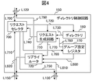
本節では、図1を用いて、本発明のマルチプロセッサシステムの動作の概要を示す。なお、説明における初期設定として、バス分割結合回路500、510、520は、500と520とが結合状態、510は分割状態だとする。つまり、CPU100とCPU200とはバスで結合されており、またCPU300とCPU400ともバスで結合されているが、CPU100&200とCPU300&400の間は分離されているとする。
Hereinafter, first, an overview of the operation of the multiprocessor system of the present invention, and then the details of the operation of the multiprocessor system of the present invention,
(1) Coherence control through the bus (2) Coherence control through the NUMA network (3) Processing when changing the bus coupling will be described in order.
[Overview of operation]
In this section, an outline of the operation of the multiprocessor system of the present invention is shown using FIG. As an initial setting in the description, it is assumed that the bus
この状態では、例えばCPU100発のキャッシュコヒーレンス要求はCPU200には部分バス140→バス分割結合回路500→部分バス240を通じて伝達することが出来る。他方、バス分割結合回路510は分割状態であるから、CPU100発のキャッシュコヒーレンス要求はバスを通じてCPU300に伝達されることはない。
In this state, for example, a cache coherence request from the
バスによるコヒーレンス制御とは別個に、ディレクトリによるコヒーレンス制御を実施する。CPU100からCPU300へのキャッシュコヒーレンス要求も、NUMAネットワーク1000を通じてであれば実施することができる。
Separately from the coherence control by the bus, the coherence control by the directory is performed. A cache coherence request from the
以上のような仕組みを生かして、次のコヒーレンス制御を実施する。
(A)バスで結合されたCPU同士で、かつキャッシュコヒーレンス制御対象のデータのアドレスがバスで結合された範囲の部分主記憶に対するものである場合には、バスでのみキャッシュコヒーレンス制御を行う。
(B)(A)以外のケースについては、NUMAネットワークを使ってキャッシュコヒーレンス制御を行う。
The following coherence control is carried out using the above mechanism.
(A) Cache coherence control is performed only on the bus if the CPUs are coupled to each other via the bus and the address of the data subject to cache coherence control is for a partial main memory in the range coupled by the bus.
(B) For cases other than (A), cache coherence control is performed using a NUMA network.
以下実例を示す。例えば、CPU100発のキャッシュコヒーレンス制御で、対象アドレスが部分主記憶180に対するものであれば、まず部分バス140→バス分割結合回路500→部分バス240を通じてCPU200に対してキャッシュコヒーレンス要求が伝達される。
An example is shown below. For example, in the cache coherence control issued by the
この要求に対して、部分主記憶180に対するアクセス情報をディレクトリ160に記憶するディレクトリ制御回路150は、ディレクトリ160に登録された情報から、もしキャッシュコヒーレンス制御がバスで結合されるCPU200に対してのみ必要と判定できれば、バスを通じてコヒーレンス制御が全て実行されていると判定し、NUMAネットワーク1000を通したキャッシュコヒーレンス制御を実行しない。ディレクトリ160に登録された情報から、もしキャッシュコヒーレンス制御がバスでは結合されないCPU300やCPU400に対しても必要と判定されれば、NUMAネットワークを通じてキャッシュコヒーレンス制御を実行する。なお、ディレクトリ制御回路150は、バスの分割結合状況をグループ設定レジスタ170に記憶している。また、ディレクトリ160には、バスで結合されていないCPU300、CPU400のアクセス情報だけでなく、バスで結合されるCPU200の情報も記憶している。部分主記憶280に対するアクセスに関しても、CPU100から見て部分主記憶280へはバスを通じてアクセスできることから、基本的には部分主記憶180(及びディレクトリ制御回路150)についてと同様の動作が部分主記憶280(及びディレクトリ制御回路250)について実行される。
In response to this request, the
上記の動作に対して、例えば、CPU100発のキャッシュコヒーレンス制御で、対象アドレスが部分主記憶380に対するものであれば、NUMA制御回路120は当該要求がバスで結合されていない部分主記憶380へのリクエストと判定し、コヒーレンス制御要求をNUMAネットワーク1000を通してディレクトリ制御回路350へ伝播する。ディレクトリ制御回路350はディレクトリ360に登録された情報に基づき、通常のNUMAによるキャッシュコヒーレンス制御を実施する。
For the above operation, for example, in the cache coherence control from the
キャッシュコヒーレンス制御動作の詳細は、別途動作詳細にて説明する。 Details of the cache coherence control operation will be described later in detail.
以上であるバス分割設定の時の定常的なキャッシュコヒーレンス制御方法の概要を説明した。次に、バス分割設定を変更する場合の動作概要を説明する。ここでは、バス分割結合回路500が結合状態から分割状態に遷移した場合を説明する。
The outline of the steady cache coherence control method at the time of the above-described bus division setting has been described. Next, an outline of the operation when changing the bus division setting will be described. Here, a case will be described in which the bus
先に述べたとおり、ディレクトリ160には、元よりCPU200のアクセス情報も登録されていることから、ディレクトリ制御回路150はグループ設定レジスタ170さえ変更すれば、CPU200に対してもNUMAネットワークを通じたキャッシュコヒーレンス制御を実行できる。故に、バス分割設定を変更する場合、バス分割結合回路500の設定を変更するだけでなく、NUMA制御回路120、220、320、420中のバス設定レジスタ130、230、330、430、及びディレクトリ制御回路150、250、350、450中のグループ設定レジスタ170、270、370、470を同時に変更する。この変更後には、今までバスを通じて行われていた、CPU100発の部分主記憶180に関するコヒーレンス制御でCPU200にのみ対する要求は、ディレクトリ制御回路150からNUMAネットワーク1000を通じてCPU200に対して実施されるようになり、また、主記憶280に関するコヒーレンス制御は、バスを使用せずNUMA制御回路120よりNUMAネットワーク1000を通じてディレクトリ260ベースで実施されるようになる。
As described above, since the access information of the
以上、バス設定が結合から分割に変更される場合の動作変更を説明したが、逆に分割から結合に変更される場合にも、基本的には上記と同様にバス分割結合回路500、510、520と同時にNUMA制御回路120、220、320、420中のバス設定レジスタ130、230、330、430、及びディレクトリ制御回路150、250、350、450中のグループ設定レジスタ170、270、370、470を変更することで、従来NUMAネットワーク1000を通じて実施されていたキャッシュコヒーレンス制御動作が結合した範囲ではバスによる動作に変更される。変更手順詳細は別途動作詳細にて説明する。
The operation change when the bus setting is changed from coupling to division has been described above. However, when the bus setting is changed from division to coupling, the bus
以上で、本発明システムの動作概要を説明した。次に、各構成要素の中身を含め、本発明システムの動作詳細を説明する。
[動作の詳細]
動作の詳細に入る前に、本発明で前提としているキャッシュコヒーレンスプロトコルを説明する。本発明では、各CPUのキャッシュコヒーレンス制御はMESIプロトコルに従うとする。MESIプロトコルでは、Cleanなデータ(=キャッシュメモリと主記憶との中身が一致しているデータ)は1CPU(Eステータス:Exclusive)もしくは複数CPU(Sステータス:Shared)が所有できるが、Modifiedデータ(=キャッシュメモリに更新された最新値があり主記憶には更新前の古い値が入っていることから中身が不一致を起こしているデータ)を所有できるのは1CPUのみ(Mステータス:Modified)というルールがある。故に、Sステータスの状態であるCPUがデータ更新を行うと、更新するCPU以外の各CPUへキャッシュ無効化要求が発生し、更新するCPUのみが更新後にMステータスでデータをキャッシュメモリに持つようになる。また、Mステータスにあるデータを他のCPUがアクセスした場合には、当該データはキャッシュメモリから主記憶に書き戻され、複数のCPUがCleanなデータをキャッシュメモリにSステータスで所有するようになる。
The outline of the operation of the system of the present invention has been described above. Next, details of the operation of the system of the present invention, including the contents of each component, will be described.
[Details of operation]
Before going into the details of the operation, the cache coherence protocol assumed in the present invention will be described. In the present invention, it is assumed that cache coherence control of each CPU follows the MESI protocol. In the MESI protocol, clean data (= data in which the contents of the cache memory and the main memory match) can be owned by one CPU (E status: Exclusive) or multiple CPUs (S status: Shared), but modified data (= There is a rule that only one CPU (M status: Modified) can have the latest value updated in the cache memory and the main memory contains the old value before the update, so that the contents are inconsistent. is there. Therefore, when a CPU in the S status state updates data, a cache invalidation request is issued to each CPU other than the CPU to be updated, and only the CPU to be updated has data in the cache memory with the M status after the update. Become. Further, when data in the M status is accessed by another CPU, the data is written back to the main memory from the cache memory, and a plurality of CPUs own the clean data in the cache memory with the S status. .
MESIプロトコルで最低限必要とされるトランザクション(=CPUから発生するデータ操作の要求)は、
・フェッチ要求(キャッシュへの新規登録)
・キャッシュ無効化要求(キャッシュデータの更新)
・キャストアウト要求(キャッシュからメモリへの書戻し)
の3つであり、本発明でも上記3つの要求がCPUから発生するとしている。
The minimum required transaction (= request for data operation generated from CPU) in the MESI protocol is as follows:
-Fetch request (new registration in the cache)
-Cache invalidation request (cache data update)
・ Castout request (write back from cache to memory)
In the present invention, the above three requests are generated from the CPU.
なお、図7中のIステータス2000はInvalidステータス(キャッシュ中のデータが無効である状態)、Eステータス2010は上記で説明したExclusiveステータス、Sステータス2030は上記で説明したSharedステータス、Mステータス2020は上記で説明したModifiedステータスである。load-miss(exclusive)とあるのは、フェッチ要求を出した結果キャッシュメモリにデータを登録したCPUが他に無いことが分かった場合、load-miss(not exclusive)とあるのは、フェッチ要求を出した結果キャッシュメモリにデータを登録したCPUが他にもあった場合、store-missはストア命令でキャッシュミスを起こしたために、一旦データをキャッシュメモリへのフェッチ要求を出し、フェッチ実行後にstoreを実行するためにキャッシュ無効化要求を出した場合を表す。
In FIG. 7, an
load-hit、store-hitはload命令、store命令を実行した時に結果としてキャッシュメモリがヒットした場合で、この場合もSステータスでstore-hitを起こした場合には、他CPUのキャッシュメモリを無効化するために、キャッシュ無効化要求を通達する必要がある。 load-hit, store-hit is a cache memory hit as a result when the load instruction, store instruction is executed. In this case, if the store-hit occurs in S status, the cache memory of the other CPU is invalidated. In order to achieve this, it is necessary to pass a cache invalidation request.
snoop-loadとあるのは他CPUからフェッチ要求を受けた場合、snoop-storeとあるのは他CPUからキャッシュ無効化要求を受けた場合である。Mステータスでsnoop-loadを受けると、主記憶にデータを書き戻すためのキャストアウトを実行する必要がある。
The snoop-load is when a fetch request is received from another CPU, and the snoop-store is when a cache invalidation request is received from another CPU. When snoop-load is received in the M status, it is necessary to execute castout for writing data back to the main memory.
上記キャッシュコヒーレンスプロトコルをベースとして、以下、最初の2節でバス分離結合設定を変更しない状態での定常的なキャッシュコヒーレンス動作をバス経由とネットワーク経由とに分けて説明し、最後の節でバス分離結合設定を変更する場合の動作について説明する。 Based on the above-mentioned cache coherence protocol, the following two sections explain the steady cache coherence operation without changing the bus separation / coupling setting in the first section. The operation for changing the combination setting will be described.
(1)バスを通したコヒーレンス制御
バスを通したコヒーレンス制御は、動作概要で説明したとおり、バスで結合されたCPU同士で、かつキャッシュコヒーレンス制御対象のデータのアドレスがバスで結合された範囲の部分主記憶に対するものである場合に行う。以下、バスを通したフェッチ要求の処理、キャッシュ無効化要求の処理、キャストアウト要求の処理を順次説明する。
(1) Coherence control through the bus As described in the operation outline, the coherence control through the bus is performed between the CPUs coupled by the bus and the address where the data address of the cache coherence control target is coupled by the bus. This is performed when it is for partial main memory. Hereinafter, processing of a fetch request through the bus, processing of a cache invalidation request, and processing of a castout request will be described in order.
(1)−1:フェッチ要求
本節では、バス分離結合回路500、510、520がそれぞれ結合、分離、結合という設定だったということを前提に、CPU100からの部分主記憶180及び部分主記憶280へのフェッチ要求がCPU200との間でどう制御されるかを説明する。
(1) -1: Fetch request In this section, it is assumed that the bus separation /
CPU100はload命令やstore命令でキャッシュメモリ110がミスを起こすと、信号線L100を通じてフェッチ要求パケットを出力する。最初に、この時のアドレスは、部分主記憶180へのリクエストであったとする。
When the
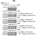
アドレスのマップについては図8に本実施例のアドレスマップを示す。各部分主記憶180、280、380、480は、その半分がローカルメモリとなっており、CPU100専用のローカル領域は部分主記憶180に、CPU200専用のローカル領域は部分主記憶280に、CPU300専用のローカル領域は部分主記憶380に、CPU400専用のローカル領域は部分主記憶480に確保される。なお、図8は各部分主記憶の容量を512メガバイトであるという前提で記載してある。図8の共有メモリ(A)4100と示されるのが部分主記憶180のローカルメモリを除いた半分、共有メモリ(B)4200と示されるのが部分主記憶280のローカルメモリを除いた半分、共有メモリ(C)4300と示されるのが部分主記憶380のローカルメモリを除いた半分、共有メモリ(D)4400と示されるのが部分主記憶480のローカルメモリを除いた半分である。故に、CPU100から見て、ローカルメモリ4000へのアクセスは部分主記憶180へのアクセス、共有メモリ(A)4100へのアクセスも部分」主記憶180へのアクセス、共有メモリ(B)4200へのアクセスが部分主記憶280へのアクセスとなる。
As for the address map, FIG. 8 shows an address map of this embodiment. Half of each partial
フェッチ要求パケットについて図9にそのフォーマットを示す。図9のうち先頭はコマンド5000であり、中身0000はフェッチ要求であることを示す。更に要求元プロセッサID5010に例えばCPU100によるキャッシュミスであれば0000、CPU200によるキャッシュミスであれば0001、CPU300によるキャッシュミスであれば0010、CPU400によるキャッシュミスであれば0011の値が入る。アドレス5020はフェッチをするアドレスである。
FIG. 9 shows the format of the fetch request packet. In FIG. 9, the head is a
以上、説明に戻るが、アドレスに対してCPU100から信号線L100に対してフェッチ要求パケットを出力したとする。NUMA制御回路は中身を図2に示すが、フェッチ要求はリクエストルータ600に到達したところで、バス設定レジスタ130の設定値とのチェックにより行き先の決定が行われる。バス設定レジスタ130の中身(32ビットとした)を図3に示すが、バス設定レジスタでは、下位4ビットを用いて(図中ビット132、134、136、138)、先程のメモリマップ上に見える共有メモリ(A)4100〜共有メモリ(D)4400が、当該NUMA制御回路から見て、それぞれバスで接続されているのか、バスは分割設定でバスではアクセス不可能なのかを表す。共有メモリ(A)4100に対応するのが最下位ビット138、共有メモリ(B)4200に対応するのがビット136、共有メモリ(C)4300に対応するのがビット134、共有メモリ(D)4400に対応するのがビット132である。中身は1であればバスで結合されているし0であればバスは分割されていることを表す。以上の設定値がバス設定レジスタ130からルータへと信号線L670を通じて伝播していることから、ルータは今回のパケットは部分主記憶180へのリクエストであると判定し、そのリクエストを信号線L610、L110を通じて部分バス140に出力する。
Returning to the description above, it is assumed that the fetch request packet is output from the
先述の通り、バス分離結合回路500は結合状態となっているので、同フェッチ要求はバス分離結合回路500を経由して部分バス240にも通達される。これにより、まずNUMA制御回路220は同リクエストを信号線L210を通じてスヌープすると、図2中(これはNUMA制御回路120の中身を示しているが、内部構成はNUMA制御回路220と同一)のセレクタ610を通してCPU200およびそのキャッシュメモリ210にフェッチ要求を通達する。
As described above, since the bus separation /
ここでスヌープした結果がミス(つまりキャッシュメモリ210には当該データが登録されていない)、もしくはメモリクリーン(つまりメモリの値が最新であったことが保障されたので、メモリからのフェッチを許可する)であれば、この情報がCPU200より信号線L200を通じてリプライされ、その信号はNUMA制御回路220内のリクエストルータ600、信号線L210を通じて部分バス240に通達され、さらにこの信号はバス分離結合回路500、部分バス140、信号線L120を通じて、当該アクセス対象となっている部分主記憶180に接続されるディレクトリ制御回路150に通知される。
Here, the result of snooping is miss (that is, the data is not registered in the cache memory 210) or memory clean (that is, the memory value is guaranteed to be the latest, so fetch from the memory is permitted. ), This information is replied from the
ディレクトリ制御回路150の内部を図4に示す。リクエストセレクタ700までは、元々フェッチ要求パケットが部分バス140に出た時点で部分主記憶180へのリクエストとして到達し、リクエストが保留されているが、このようにリクエストが保留されると同時に信号線L720を通じてディレクトリ160を検索する動作を行う。ディレクトリ160は、CPU100、200、300、400が主記憶をアクセスする単位(キャッシュブロックと一般に言う)毎に図5に示すようなエントリを用意するものであり(つまりディレクトリ160の中には図5に示されるようなエントリが多数入っている)、図5のビット162が1であることは当該ブロックがCPU100によりキャッシュメモリに登録された(ことが過去にあり、まだキャッシュメモリに残っている可能性があるということ。正確にはキャッシュメモリから既に消滅している可能性もあるが、ディレクトリではキャッシュメモリに登録されていることになる)ことを表し、同様にビット164はCPU200に、ビット166はCPU300に、ビット168はCPU400に対応する。
The inside of the
図5の例ではCPU100、200、300によりアクセスされていることになるが、本節の事例では、このパタンではなく、値が0100であったとする。つまり、他CPUについては、CPU200のみ当該データをキャッシュに取り込んでいる可能性があるとする。この信号が信号線L730を通じてリクエスト生成回路710に入るとリクエスト生成回路710は別途信号線780と通じて入るグループ設定レジスタ170の値と比較する。
In the example of FIG. 5, the
グループ設定レジスタ170の中身を図6に示す。グループ設定レジスタ170は32ビットのレジスタで、上位4ビットにCPU100、200、300、400に対応したビット172、174、176、178を持つ。それぞれのCPUが当該ディレクトリ制御回路から見てバスで結合されている場合は1、バスが分離されている場合は0が登録されている。
The contents of the
リクエスト生成回路は710は、図6のような情報から、ディレクトリ160でチェックされたCPU200がバスで結合されていることを判定できる。この場合は信号線L740を通じてリクエストセレクタ700にCPU200からのリプライを待つよう通達する。なお、もしディレクトリの値が0110でCPU300も当該データをキャッシュに登録していることになっている場合には、同時にリクエスト生成回路710は信号線740、リクエストセレクタ700、信号線L710、L150を通じてNUMAネットワーク1000経由でのキャッシュコヒーレンス制御も行うことになるが、これについては(2)節で詳しく説明するので、本節では前述の通りディレクトリの値は0100であったとして説明を続ける。
The
先述の通り、当該キャッシュブロックはディレクトリ160によりCPU200のキャッシュに登録された可能性があったが、CPU200よりキャッシュミスもしくはメモリクリーンのリプライがリクエストセレクタ700まで到達することで、リクエストセレクタ800は当該フェッチ要求に対しては部分主記憶180をアクセスすべきであることが判定できることから、信号線L720を通じてディレクトリ160へのCPU100分の登録を通知するとともに(これにより当該ディレクトリエントリの値は0100から1100に変更される)、信号線L750、L130を通じて部分主記憶180へフェッチリクエストを出力する。部分主記憶180はこれに対して図11に示されるフェッチリプライパケットを返答する。フェッチリプライパケットは、パケットのコマンド5200が値0010で、要求元プロセッサID5210(=リプライ送付先プロセッサID)を持ち、これとフェッチしたデータ本体5220(キャッシュブロック分のサイズを持つ)とから成る。
As described above, there is a possibility that the cache block is registered in the cache of the
このフェッチリプライパケットは、信号線L130から図4中の信号線L810、リプライルータ720、信号線L790、L120、部分バス140に出力され、更に信号線L110から図2中信号線L630を通じてセレクタ610に渡り、ここから信号線L680、L100を経由してキャッシュメモリ110及びCPU100へとリプライデータが戻る。
The fetch reply packet is output from the signal line L130 to the signal line L810, the
以上は、CPU200の返答がミスもしくはメモリクリーンであり、主記憶からデータを読むケースであったが、これがCPU200が図7中のMステータス2020であり(つまり最新のデータはCPU200のキャッシュメモリ210に存在する)、CPU200のキャッシュメモリ210に登録されているデータをCPU100が読み出す必要があるケースを次に説明する。
The above is a case where the response of the
この場合はミスもしくはメモリクリーンのステータスではなく、
CPU200からはキャストアウトパケットが出力される。キャストアウトパケットを図10に示す。コマンド5100は0001であり、その他に要求元プロセッサID5110(=書き込み元プロセッサIDであり今回の場合で言えばCPU200)、書き戻すべきアドレス5120、キャッシュブロック分のデータ5130から成る。
This is not a miss or memory clean status,
A cast-out packet is output from the
キャストアウトパケットはミスもしくはメモリクリーンのステータスと同様にディレクトリ制御回路150のリクエストセレクタ700に到達すると、信号線L750、L130を通じて部分主記憶180にデータを書き戻す。リクエストセレクタ700は、この書き戻し動作を待ち、後は前述ミスもしくはメモリクリーンのステータスの時と同様に部分主記憶180からデータを読み出す。(この際にディレクトリ160の当該エントリを0100から1100に変更することも前述の通りである)
なお、本節では部分主記憶180に対するアクセスについて説明したが、同様にバスで結合される部分主記憶280へのアクセスの場合も、ディレクトリ制御回路150の代わりにディレクトリ制御回路250が主体となるだけで、その動作は基本的に同一となる。
When the cast-out packet reaches the
In this section, access to the partial
(1)−2:キャッシュ無効化要求
本節では、CPU100が既にキャッシュメモリ110に登録しているデータ(他のCPUとの共有があり、キャッシュステータスは図7のSステータス2030である)に対してストアを実行する場合、他のCPUのキャッシュメモリをキャンセルする必要が発生する。本節では、この動作について説明する。なお、本節ではキャッシュ登録データの共有はCPU100とCPU200とで行われているとし、対象となるデータは部分主記憶180中に存在するものとする。つまり、ディレクトリ160の、当該データに対するエントリの値(図5相当)は1100であるとする。
(1) -2: Cache Invalidation Request In this section, for data that the
前節同様にしてキャッシュ無効化要求パケットがまずCPU100から信号線L100を通して出力される。キャッシュ無効化要求パケットを図12に示す。コマンド5300は0011、要求元プロセッサID5310は今回の場合はCPU100を示し、要求先プロセッサID5320は、CPU100から出力された時はNull(ここでは2進数でオール1とする)となる。要求先プロセッサID5310はNUMAネットワークを通じたコヒーレンス制御の際に意味のある値が入るフィールドであり、本節ではNullのままである。キャッシュ無効化要求パケットは更に無効化するアドレス5330を持つ。
As in the previous section, a cache invalidation request packet is first output from the
キャッシュ無効化要求パケットは、前節のフェッチ要求パケット同様にCPU100からCPU200及びディレクトリ制御回路150に伝達されるが、処理内容は次の3点が異なる。一つ目の違いは、CPU200に伝達された結果はキャッシュのミスやメモリクリーンステータスの代わりに、キャッシュ無効化成功のステータスが返されること。二つ目の違いは、ディレクトリ制御回路は、ステータスが帰っても部分主記憶180へのアクセスを行わず、単にディレクトリ160の値の再設定を行うのみであること(本例では、1100から1000に変更)。三つ目の違いはCPU100へはフェッチデータが返る代わりにキャッシュ無効化完了のステータスが返ること。
The cache invalidation request packet is transmitted from the
なお、前節同様、部分主記憶180のデータに対するキャッシュ無効化も、同様にバスで結合される部分主記憶280のデータに対するキャッシュ無効化も、ディレクトリ制御回路150の代わりにディレクトリ制御回路250が主体となるだけで、その動作は基本的に同一となる。
As in the previous section, both the cache invalidation for the data in the partial
(1)−3:キャストアウト要求
Mステータス2020で登録していた情報を、他の新しいデータをキャッシュメモリ110に登録するために主記憶に書き戻す必要が発生した場合の動作を説明する(ここでは前節までと同様に部分主記憶180に対する書き戻し要求であるとする)。なお、Mステータス2020でデータを所有しているということは、同一キャッシュブロックを登録している可能性のあるCPUは他に無いことを表しているので、ディレクトリ160の当該エントリの値は1000となる。
(1) -3: Cast-out request The operation when the information registered in the
キャストアウトの場合も、最初にCPU100がキャストアウト要求パケットを信号線L100を通して出力する。キャストアウト要求パケットについては、(1)−1で図10を用いて説明した通りのフォーマットであり、今回のパタンでは要求元プロセッサIDにはCPU100が入る。
Also in the case of cast-out, the
キャストアウトは基本的には主記憶に対してデータを書き戻すだけのアクションであり、CPU間でのコヒーレンス制御は不要なので、キャストアウト要求パケットはフェッチ要求パケット同様にディレクトリ制御回路150に到達した後は、他のCPUのコヒーレンス制御を待つことなく、速やかに部分主記憶180への書き戻しを行う。具体的には図4のリクエストセレクタ700でコヒーレンス操作の完了を待つことなく、信号線L750、L130を通じて速やかに部分主記憶180へ書き戻す。
Castout is basically an action that only writes data back to the main memory, and coherence control between CPUs is unnecessary. Therefore, a castout request packet arrives at the
なお、本アクションにおけるディレクトリ160の操作だが、キャストアウトが実行される場合は基本的には当該CPU100のキャッシュメモリ110からは当該キャッシュデータブロックは消滅するので、ディレクトリ160のエントリの値は1000から0000に変更しても良い。但し、特別の命令を使用することで、キャッシュメモリ110から消滅させずにキャストアウトが実行できるような場合には、ディレクトリ160のエントリの値は1000のままとする必要がある。本実施例では後者を前提とし、ディレクトリ160は変更しないとする。
In this action, although the operation of the
前節同様、部分主記憶180のデータに対するキャストアウトも、同様にバスで結合される部分主記憶280のデータに対するキャストアウトも、ディレクトリ制御回路150の代わりにディレクトリ制御回路250が主体となるだけで、その動作は基本的に同一となる。
As in the previous section, the cast-out for the data in the partial
なお、本節ではCPU100が自分自身の都合でキャストアウトする場合を説明したが、他CPUからのフェッチ要求を受けてキャストアウトする場合の動作については、バスで結合された範囲については(1)−1で説明した通りである。バスが分離された範囲については次節で説明する。
In this section, the case where the
(2)NUMAネットワークを通したコヒーレンス制御
前述の通り、バスで結合されたCPU同士でない場合、もしくはバスで結合されたCPU同士でも、キャッシュコヒーレンス制御対象のデータのアドレスがバスで結合された範囲の部分主記憶に対するものでない場合は、NUMAネットワーク1000を通したキャッシュコヒーレンス制御となる。
(2) Coherence control through the NUMA network As described above, when the CPUs are not coupled to each other via the bus, or even between the CPUs coupled via the bus, the address of the data subject to cache coherence control is within the range coupled via the bus. If it is not for partial main memory, cache coherence control through the
本節では、NUMAネットワーク1000を通したコヒーレンス制御について、バスを通した制御との差分を中心に説明する。
In this section, the coherence control through the
(2)−1:フェッチ要求
ここでは、まずバスで結合されていない部分主記憶に対してNUMAネットワークを経由してフェッチ要求を発行する場合を説明する。この動作はNUMA制御回路120、220、320、420にて、フェッチ要求リクエストのアドレスとバス設定レジスタ130、230、330、430の値との関係で、バスが結合されていないことをNUMA制御回路内のリクエストルータ600で判定した場合、従来バスに信号線L610、L110を経由して出力していたフェッチ要求パケットを信号線L620、L140を経由してNUMAネットワーク1000へ出力する。NUMAネットワークはパケットの要求先アドレス5020を用いて行き先を例えば部分主記憶380と判定するとその部分主記憶に対応するディレクトリ制御回路350へとパケットを伝達する。 ディレクトリ制御回路内のリクエストセレクタ700に伝達された先は、基本的にディレクトリ160の情報を用いてコヒーレンス制御を行う基本概念は(1)−1節と同一だが、フェッチ要求パケットはバス経由で入ってきたのではないことから、ディレクトリを検索した結果、全てのコヒーレンス制御パケットをディレクトリ生成回路710で生成し、リプライルータ720、信号線L820、L150を経由して、コヒーレンス制御パケットもまたNUMAネットワーク1000を用いて対象プロセッサに分配しなければならない。分配したパケットはNUMA制御回路120、220、320、420に入り、セレクタ610を経由して各CPU100、200、300、400に通達される。この結果例えばMステータスのデータを持ったCPUが存在し、キャッシュメモリ上のデータを部分主記憶に書き戻す必要が出た場合にも、NUMA制御回路120、220、320、420を経由してNUMAネットワーク1000を通って書き戻す。
(2) -1: Fetch Request Here, a case where a fetch request is issued via a NUMA network to partial main memories that are not coupled via a bus will be described first. In this operation, the
要は、バスで結合されていない部分主記憶に対してNUMAネットワークを経由してフェッチ要求を発行する場合については、前節でバスを経由して実行していた動作全てが、基本的にNUMAネットワーク1000を経由して実行されることになる。 In short, when issuing a fetch request via the NUMA network to the partial main memory not connected by the bus, all the operations executed via the bus in the previous section are basically the NUMA network. 1000 will be executed.
NUMAネットワークを経由するフェッチ要求については、バスで結合される部分主記憶180、280、380、480に対するフェッチ要求だったが、ディレクトリ160、260、360、460を検索した結果、バスで結合されないCPU100、200、300、400もキャッシュメモリ110、210、310、410に登録しているケースがある。この場合には、(1)−1節でディレクトリ制御回路150内で、ディレクトリ160を検索した結果、CPU200のキャッシュメモリへの登録が分かり、リクエストセレクタ700に、バス結合されたCPU200についてのキャッシュコヒーレンス制御解消を待ってフェッチ要求パケットを保留していた部分の動作に次の変更が加わる。すなわち、ディレクトリ160を検索した結果、バスで結合されないCPU,例えばCPU300がキャッシュメモリに登録していることが判明した時点で、リクエスト生成回路710よりフェッチ要求パケットを生成し、リプライルータ720、信号線820、L150、NUMAネットワーク1000を経由して、NUMA制御回路320経由でCPU300に伝達し、このCPU300からのリプライが再びNUMA制御回路320及びNUMAネットワーク1000を経由してディレクトリ制御回路150に返答されるまでリクエストセレクタ700にリクエストを保持することになる。本リクエストの結果、CPU300からキャストアウト要求が発生した場合にも、同様にNUMA制御回路320とNUMAネットワーク1000を経由して、ディレクトリ制御回路にそのキャストアウト要求が伝播し、これを部分主記憶180に書き戻してからフェッチ動作をディレクトリ制御回路150が実行することになる。
The fetch request via the NUMA network is a fetch request for the partial
ディレクトリ160、260、360、460への設定内容については、(1)節と同様に、新たにフェッチを行ったCPUを新たにディレクトリに登録することになる。
As for the setting contents in the
(2)−2:キャッシュ無効化要求
NUMAネットワーク1000経由のキャッシュ無効化要求には、(2)−1と同様に、バスで結合されていない部分主記憶のデータに対するキャッシュ無効化要求の場合と、バスで結合されている部分主記憶のデータに対するキャッシュ無効化要求がバスで結合されていないCPUに対して発生するケースとがある。それぞれ基本的には(2)−1と同様であるが、但しフェッチリプライの代わりに、図13で示されるキャッシュ無効化完了パケットが返答されてくることになる。
(2) -2: Cache invalidation request Similarly to (2) -1, the cache invalidation request via the
本動作を行った場合にも(1)−2同様に、当該ディレクトリエントリの値は、キャッシュ無効化要求を行った1CPU以外は全て0に戻される。 Even when this operation is performed, the value of the directory entry is returned to 0 except for 1 CPU that has requested cache invalidation, as in (1) -2.
(2)−3:キャストアウト要求
NUMAネットワーク1000経由のキャストアウトは、バスが分離されてる部分主記憶180、280、380、480への書き戻しの際に発生するが、これもCPU100、200、300、400から書き戻し要求がNUMA制御回路120、220、320、420に伝達されると、バス設定レジスタ130、230、330、430の値に応じてリクエストルータ600によりNUMAネットワーク1000への出力が選択され、このキャストアウト要求パケットはNUMAネットワーク1000からディレクトリ制御回路150、250、350、450を経由して部分主記憶180、280、380、480に書き戻される。本実施例ではキャストアウトによる書き戻しの際にディレクトリの設定値を変更しないとしたが((1)−3参照)、NUMAネットワーク1000経由のキャストアウトでもこれは同じである。
(2) -3: Cast-out request Cast-out via the
(3)バス結合の変更時の処理
(1)(2)の動作により、ディレクトリ制御回路150、250、350、450内のディレクトリ160、260、360、460には、バス分離・結合に関わらず、当該データブロックをキャッシュメモリに登録してうる全てのCPUが登録されている。これにより、バス結合の状態が変更されても、変更後のバスの結合・分離に従ってディレクトリ160、260、360、460に従ったキャッシュコヒーレンス制御(バスで接続されるCPUの組についてはバスでの制御期待でNUMAネットワーク経由の制御なし)が実現できる。
(3) Processing at the time of changing the bus coupling (1) By the operation of (2), the
本節では、バス接続形態を変更する際の動作を図1を用いて更に説明する。例えばCPU100がバスの接続形態を変更したい場合には、まず信号線L10を通してサービスプロセッサ10に要求を通達する。サービスプロセッサは要求CPU100以外のCPU200、300、400を信号線L30、L50、L70を通じてストップさせ、これが完了するとバス分離結合回路500、510、520の設定値を変えるとともに、その変更の完了をCPU100に通知する。
In this section, the operation when changing the bus connection mode will be further described with reference to FIG. For example, when the
CPU100は、アドレス空間上に図8の通りマップされるバス設定レジスタ(A)〜(D)、グループ設定レジスタ(A)〜(D)(実体は、バス設定レジスタ130、230、330、430およびグループ設定レジスタ170、270、370、470をバス接続形態に応じた値に変更する。
The
なお、各レジスタへのアクセスは、(バスの接続形態がどう変化するか設定値により変わりうるために)設定値によらず、全てNUMAネットワーク1000を経由して実行される。例えばCPU100がバス設定レジスタ230を更新する場合には、NUMA制御回路120にて当該リクエストはNUMAネットワーク経由と判定され、NUMAネットワーク経由でNUMA制御回路220中のバス設定レジスタ230を設定することになる。
Note that access to each register is performed via the
以上の通り、バス分割結合回路500、510、520はサービスプロセッサ10が、バス設定レジスタ130、230、330、430及びグループ設定レジスタ170、270、370、470はCPU100、200、300、400自身が変更することにより、バスの分離結合形態に関する全ての設定が変更できる。変更後にサービスプロセッサ10を経由して全てのCPU100、200、300、400の動作を再開すると、以降変更後のバスの形態に従い、正しいキャッシュコヒーレンス制御が実行されることになる。
As described above, the bus
実施例1では、NUMA制御用に専用のNUMAネットワーク1000が存在することを前提としたが、以下にのべる実施例2では、NUMAネットワーク1000の代わりに、NUMAプロトコル用のパケットもバスを経由して実行される。
In the first embodiment, it is assumed that a
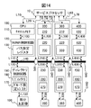
図14に実施例2のシステム構成を示す。図1に示される実施例1との違いは3点ある。 FIG. 14 shows a system configuration of the second embodiment. There are three differences from the first embodiment shown in FIG.
第1点目は、バス分割結合回路500、510、520をバスフィルター回路505、515、525に置き換えたことである。バスフィルター回路505、515、525は、NUMA制御用以外のパケットに対してはバス分割結合回路500、510、520と同様に機能する(つまりサービスプロセッサ10による設定により、パケットを通したり通さなくなったりする)が、NUMA制御用パケットに対しては、常にこれを通す機能を持つ。
The first point is that the bus
第2点目は、実施例1では例えばフェッチ要求パケットはバス結合のCPUの間でもNUMAネットワークでの結合のCPUの間でも、同じコマンド(0000)を使用していたが、これだとバスフィルター回路505、515、525がNUMA制御用とそれ以外との分類が出来なくなることを考慮し、最上位1ビットを1とするように変更する。つまり、バス間のフェッチリクエストではコマンドは0000だが、NUMA接続のプロセッサの間でのフェッチ要求パケットはコマンドを1000とすることになる。なお、本変更はNUMA制御回路120内のリクエストルータ600、及びディレクトリ制御回路150内のリクエスト生成回路710を変更することで実現する。
The second point is that in the first embodiment, for example, the fetch request packet uses the same command (0000) between the CPUs connected to the bus and the CPUs connected to the NUMA network. Considering that the
第3点目は、実施例1ではNUMAネットワーク1000に対してNUMA制御パケットをやり取りしていたNUMA制御回路120、220、320、420及びNUMAディレクトリ制御回路150、250、350、450のNUMAネットワーク1000への入出力の口を全て部分バス140、240、340、440に対する口と統合することである。
The third point is that the
なお、構成上の上記3点の変更とは別だが、実施例1でNUMA制御パケットがNUMAネットワーク1000により1対1で実行されていたことに対し、実施例2の構成では、パケットの伝達という観点だけで見れば、部分バス140、240、340、440の全てにNUMA制御パケットがブロードキャストされてしまうことがある。但し、実際にはアドレスやプロセッサIDにより各パケットは1対1で機能することから、実質的なパケットの処理については実施例1と差異はない。
Although different from the above three changes in configuration, the NUMA control packet is executed on a one-to-one basis by the
NUMA制御パケットがブロードキャスト伝達されてしまうことで、バスの上での輻輳が増加する危険があるが、ジョブの実行形態(例えば、あるユーザJOBをCPU100とCPU200とで並列実行する)に即したパーティションの設定(前述の例であればCPU100とCPU200とを同一のパーティションに設定する、つまり部分バス140と部分バス240との間は完全結合し、全てのリクエストを通す。但し部分バス240と部分バス340とはフィルターをかけ、NUMA制御パケットのみを通す設定とする)をすることで、実質的にNUMA制御パケットの発生頻度は著しく低減されるので、NUMA制御パケットのブロードキャストによる性能低下は問題にならない。
There is a risk that congestion on the bus increases due to broadcast transmission of a NUMA control packet, but a partition conforming to a job execution mode (for example, a user JOB is executed in parallel by the
上記の通り、NUMAネットワーク1000で制御していたパケットを部分バス140、240、340、440で伝達することにより、CPU間のネットワーク接続無しに本発明の特徴である性能のスケーラビリティを確保しながら、パーティション設定にも自由度があるマルチプロセッサが実現することになる。
As described above, by transmitting the packet controlled by the
200、300、400…CPU
210、310、410…キャッシュメモリ
220、320、420…NUMA制御回路
230、330、430…バス設定レジスタ
140、240、340、440…部分バス
250、350、450…ディレクトリ制御回路
260、360、460…ディレクトリ
270、370、470…グループ設定レジスタ
280、380、480…部分主記憶
132、134、136、138…バス設定ビット
162、164、166、168…ディレクトリビット
172、174、176、178…グループ設定ビット
500、510、520…バス分割結合回路
505、515、525…バスフィルター回路
5000、5100、5200、5300、5400…コマンド
L10〜L800…信号線。
200, 300, 400 ... CPU
210, 310, 410 ...
Claims (8)
キャッシュコヒーレンス要求をバス経由で各プロセッサにブロードキャストすることでキャッシュコヒーレンス制御を実現する手段と、
前記バスでのブロードキャストの範囲をシステム全体ではなくシステムの一部になるように該バスを分割設定する手段とを有し、
前記主記憶に対応して該主記憶の各データブロック毎にそのデータブロックをキャッシュメモリに登録したプロセッサのIDを記録するディレクトリを有し、
前記ディレクトリに記録されたIDの情報を用いて各プロセッサの間でキャッシュコヒーレンス制御を行う手段を有し、
前記バスで結合されるプロセッサ間は前記バスを介したキャッシュコヒーレンス要求の伝達によるキャッシュコヒーレンス制御を行い、
該バスの分割設定により互いに分断されたプロセッサ間では前記ディレクトリを用いたキャッシュコヒーレンス制御を行うことを特徴とするマルチプロセッサシステム。 A multiprocessor system having a plurality of processors each having a cache memory and a main memory shared by the plurality of processors,
Means for realizing cache coherence control by broadcasting a cache coherence request to each processor via a bus;
Means for dividing and setting the bus so that the range of the broadcast on the bus becomes a part of the system rather than the entire system,
Corresponding to the main memory, each data block of the main memory has a directory for recording the ID of the processor that registered the data block in the cache memory,
Means for performing cache coherence control between the processors using the ID information recorded in the directory;
Cache coherence control is performed between the processors coupled by the bus by transmitting a cache coherence request via the bus,
A multiprocessor system, wherein cache coherence control using the directory is performed between processors separated from each other by the division setting of the bus.
キャッシュコヒーレンス要求をバス経由で各プロセッサにブロードキャストすることでキャッシュコヒーレンス制御を実現する手段と、
前記バスでのブロードキャストの範囲をシステム全体ではなくシステムの一部になるように該バスを分割設定する手段とを有し、
前記部分主記憶の各々に対応して設けれら、各部分主記憶のデータブロック毎にそのデータブロックをキャッシュメモリに登録したプロセッサのIDを記録するディレクトリを有し、
前記ディレクトリに記録されたIDの情報を用いて各プロセッサの間でキャッシュコヒーレンス制御を行う手段を有し、
分割設定された前記バスで相互に結合されたプロセッサに対応する範囲の部分主記憶に含まれるデータに対するキャッシュコヒーレンス制御で、かつ該相互に結合されたプロセッサ間のキャッシュコヒーレンス制御の場合に、前記バスを用いたキャッシュコヒーレンス制御を行い、
前記バスの分割設定で分断されたプロセッサ間、もしくは前記バスで結合されたプロセッサ間であってもキャッシュコヒーレンス制御対象のデータが前記結合されたプロセッサに対応する範囲の部分主記憶ではなく、該範囲から外れる部分主記憶に含まれる場合には該ディレクトリを用いたキャッシュコヒーレンス制御を行うことを特徴とするマルチプロセッサシステム。 A plurality of processors each having a cache memory, and a plurality of partial main memories that are shared by the plurality of processors and provided respectively corresponding to each of the plurality of processors or processor groups A multiprocessor system having storage,
Means for realizing cache coherence control by broadcasting a cache coherence request to each processor via a bus;
Means for dividing and setting the bus so that the range of the broadcast on the bus becomes a part of the system rather than the entire system,
Provided corresponding to each of the partial main memory, for each data block of the partial main storage, having a directory for recording the ID of the processor that registered the data block in the cache memory,
Means for performing cache coherence control between the processors using the ID information recorded in the directory;
In the case of cache coherence control for data included in a partial main memory in a range corresponding to processors coupled to each other by the bus set to be divided, and in the case of cache coherence control between the mutually coupled processors, the bus Cache coherence control using
Cache coherence control target data is not a partial main memory in the range corresponding to the combined processor, even between the processors divided by the bus division setting or between the processors connected by the bus. A multiprocessor system that performs cache coherence control using the directory when it is included in a partial main memory that is out of scope.
Priority Applications (2)
| Application Number | Priority Date | Filing Date | Title |
|---|---|---|---|
| JP2003379294A JP4507563B2 (en) | 2003-11-10 | 2003-11-10 | Multiprocessor system |
| US10/886,036 US7159079B2 (en) | 2003-11-10 | 2004-07-08 | Multiprocessor system |
Applications Claiming Priority (1)
| Application Number | Priority Date | Filing Date | Title |
|---|---|---|---|
| JP2003379294A JP4507563B2 (en) | 2003-11-10 | 2003-11-10 | Multiprocessor system |
Publications (2)
| Publication Number | Publication Date |
|---|---|
| JP2005141606A JP2005141606A (en) | 2005-06-02 |
| JP4507563B2 true JP4507563B2 (en) | 2010-07-21 |
Family
ID=34544517
Family Applications (1)
| Application Number | Title | Priority Date | Filing Date |
|---|---|---|---|
| JP2003379294A Expired - Fee Related JP4507563B2 (en) | 2003-11-10 | 2003-11-10 | Multiprocessor system |
Country Status (2)
| Country | Link |
|---|---|
| US (1) | US7159079B2 (en) |
| JP (1) | JP4507563B2 (en) |
Families Citing this family (15)
| Publication number | Priority date | Publication date | Assignee | Title |
|---|---|---|---|---|
| US7437617B2 (en) * | 2005-02-11 | 2008-10-14 | International Business Machines Corporation | Method, apparatus, and computer program product in a processor for concurrently sharing a memory controller among a tracing process and non-tracing processes using a programmable variable number of shared memory write buffers |
| US7437618B2 (en) * | 2005-02-11 | 2008-10-14 | International Business Machines Corporation | Method in a processor for dynamically during runtime allocating memory for in-memory hardware tracing |
| US7418629B2 (en) * | 2005-02-11 | 2008-08-26 | International Business Machines Corporation | Synchronizing triggering of multiple hardware trace facilities using an existing system bus |
| JP4945200B2 (en) * | 2006-08-29 | 2012-06-06 | 株式会社日立製作所 | Computer system and processor control method |
| US8140817B2 (en) * | 2009-02-24 | 2012-03-20 | International Business Machines Corporation | Dynamic logical partition management for NUMA machines and clusters |
| JP5568939B2 (en) * | 2009-10-08 | 2014-08-13 | 富士通株式会社 | Arithmetic processing apparatus and control method |
| EP2546744B1 (en) | 2010-03-11 | 2017-05-10 | Fujitsu Limited | Software control device, software control method, and software control program |
| JP5623259B2 (en) | 2010-12-08 | 2014-11-12 | ピーエスフォー ルクスコ エスエイアールエルPS4 Luxco S.a.r.l. | Semiconductor device |
| US9478502B2 (en) * | 2012-07-26 | 2016-10-25 | Micron Technology, Inc. | Device identification assignment and total device number detection |
| US9237093B2 (en) * | 2013-03-14 | 2016-01-12 | Silicon Graphics International Corp. | Bandwidth on-demand adaptive routing |
| US10944694B2 (en) | 2016-12-06 | 2021-03-09 | Hewlett Packard Enterprise Development Lp | Predictive arbitration circuit |
| US10452573B2 (en) | 2016-12-06 | 2019-10-22 | Hewlett Packard Enterprise Development Lp | Scripted arbitration circuit |
| US10237198B2 (en) | 2016-12-06 | 2019-03-19 | Hewlett Packard Enterprise Development Lp | Shared-credit arbitration circuit |
| US10721185B2 (en) | 2016-12-06 | 2020-07-21 | Hewlett Packard Enterprise Development Lp | Age-based arbitration circuit |
| US10693811B2 (en) | 2018-09-28 | 2020-06-23 | Hewlett Packard Enterprise Development Lp | Age class based arbitration |
Citations (2)
| Publication number | Priority date | Publication date | Assignee | Title |
|---|---|---|---|---|
| JP2000250882A (en) * | 1999-02-26 | 2000-09-14 | Internatl Business Mach Corp <Ibm> | Method and system for avoiding lie block caused by collision of invalid transaction in unequal memory access system |
| JP2002304328A (en) * | 2001-02-15 | 2002-10-18 | Bull Sa | Coherence controller for multi-processor system, module incorporating the same, and multi-module architecture multi-processor system |
Family Cites Families (6)
| Publication number | Priority date | Publication date | Assignee | Title |
|---|---|---|---|---|
| JPH05108578A (en) * | 1991-10-19 | 1993-04-30 | Fuji Xerox Co Ltd | Information processing system |
| JPH0816474A (en) * | 1994-06-29 | 1996-01-19 | Hitachi Ltd | Multiprocessor system |
| JP3872118B2 (en) * | 1995-03-20 | 2007-01-24 | 富士通株式会社 | Cache coherence device |
| US5673413A (en) * | 1995-12-15 | 1997-09-30 | International Business Machines Corporation | Method and apparatus for coherency reporting in a multiprocessing system |
| JPH09198309A (en) * | 1996-01-17 | 1997-07-31 | Canon Inc | Information processing system, system control method and information processor |
| JP3849951B2 (en) | 1997-02-27 | 2006-11-22 | 株式会社日立製作所 | Main memory shared multiprocessor |
-
2003
- 2003-11-10 JP JP2003379294A patent/JP4507563B2/en not_active Expired - Fee Related
-
2004
- 2004-07-08 US US10/886,036 patent/US7159079B2/en not_active Expired - Fee Related
Patent Citations (2)
| Publication number | Priority date | Publication date | Assignee | Title |
|---|---|---|---|---|
| JP2000250882A (en) * | 1999-02-26 | 2000-09-14 | Internatl Business Mach Corp <Ibm> | Method and system for avoiding lie block caused by collision of invalid transaction in unequal memory access system |
| JP2002304328A (en) * | 2001-02-15 | 2002-10-18 | Bull Sa | Coherence controller for multi-processor system, module incorporating the same, and multi-module architecture multi-processor system |
Also Published As
| Publication number | Publication date |
|---|---|
| US20050102477A1 (en) | 2005-05-12 |
| JP2005141606A (en) | 2005-06-02 |
| US7159079B2 (en) | 2007-01-02 |
Similar Documents
| Publication | Publication Date | Title |
|---|---|---|
| JP3722415B2 (en) | Scalable shared memory multiprocessor computer system with repetitive chip structure with efficient bus mechanism and coherence control | |
| JP3661761B2 (en) | Non-uniform memory access (NUMA) data processing system with shared intervention support | |
| US7363462B2 (en) | Performing virtual to global address translation in processing subsystem | |
| JP3644587B2 (en) | Non-uniform memory access (NUMA) data processing system with shared intervention support | |
| US7577794B2 (en) | Low latency coherency protocol for a multi-chip multiprocessor system | |
| JP4848771B2 (en) | Cache coherency control method, chipset, and multiprocessor system | |
| KR100465583B1 (en) | Non-uniform memory access(numa) data processing system that speculatively forwards a read request to a remote processing node and communication method in the system | |
| US7765381B2 (en) | Multi-node system in which home memory subsystem stores global to local address translation information for replicating nodes | |
| US6636949B2 (en) | System for handling coherence protocol races in a scalable shared memory system based on chip multiprocessing | |
| US6826653B2 (en) | Block data mover adapted to contain faults in a partitioned multiprocessor system | |
| JP4507563B2 (en) | Multiprocessor system | |
| US20040093455A1 (en) | System and method for providing forward progress and avoiding starvation and livelock in a multiprocessor computer system | |
| US6266743B1 (en) | Method and system for providing an eviction protocol within a non-uniform memory access system | |
| US6279085B1 (en) | Method and system for avoiding livelocks due to colliding writebacks within a non-uniform memory access system | |
| JP2000010860A (en) | Cache memory control circuit, processor, processor system, and parallel processor system | |
| WO2014146424A1 (en) | Method for server node data caching based on limited data coherence state | |
| JP2001282764A (en) | Multiprocessor system | |
| US8332592B2 (en) | Graphics processor with snoop filter | |
| US6226718B1 (en) | Method and system for avoiding livelocks due to stale exclusive/modified directory entries within a non-uniform access system | |
| EP1611513B1 (en) | Multi-node system in which global address generated by processing subsystem includes global to local translation information | |
| JP3626609B2 (en) | Multiprocessor system | |
| US20110138101A1 (en) | Maintaining data coherence by using data domains | |
| JPH09311820A (en) | Multiprocessor system | |
| JP6631317B2 (en) | Arithmetic processing device, information processing device, and control method for information processing device | |
| US20020152358A1 (en) | Always succeeding change to dirty method |
Legal Events
| Date | Code | Title | Description |
|---|---|---|---|
| RD04 | Notification of resignation of power of attorney |
Free format text: JAPANESE INTERMEDIATE CODE: A7424 Effective date: 20060424 |
|
| A621 | Written request for application examination |
Free format text: JAPANESE INTERMEDIATE CODE: A621 Effective date: 20061006 |
|
| A977 | Report on retrieval |
Free format text: JAPANESE INTERMEDIATE CODE: A971007 Effective date: 20100203 |
|
| A131 | Notification of reasons for refusal |
Free format text: JAPANESE INTERMEDIATE CODE: A131 Effective date: 20100216 |
|
| A521 | Request for written amendment filed |
Free format text: JAPANESE INTERMEDIATE CODE: A523 Effective date: 20100315 |
|
| TRDD | Decision of grant or rejection written | ||
| A01 | Written decision to grant a patent or to grant a registration (utility model) |
Free format text: JAPANESE INTERMEDIATE CODE: A01 Effective date: 20100413 |
|
| A01 | Written decision to grant a patent or to grant a registration (utility model) |
Free format text: JAPANESE INTERMEDIATE CODE: A01 |
|
| A61 | First payment of annual fees (during grant procedure) |
Free format text: JAPANESE INTERMEDIATE CODE: A61 Effective date: 20100426 |
|
| FPAY | Renewal fee payment (event date is renewal date of database) |
Free format text: PAYMENT UNTIL: 20130514 Year of fee payment: 3 |
|
| FPAY | Renewal fee payment (event date is renewal date of database) |
Free format text: PAYMENT UNTIL: 20130514 Year of fee payment: 3 |
|
| FPAY | Renewal fee payment (event date is renewal date of database) |
Free format text: PAYMENT UNTIL: 20130514 Year of fee payment: 3 |
|
| LAPS | Cancellation because of no payment of annual fees |