JP4478680B2 - Transmit / receive signal interface - Google Patents
Transmit / receive signal interface Download PDFInfo
- Publication number
- JP4478680B2 JP4478680B2 JP2006520285A JP2006520285A JP4478680B2 JP 4478680 B2 JP4478680 B2 JP 4478680B2 JP 2006520285 A JP2006520285 A JP 2006520285A JP 2006520285 A JP2006520285 A JP 2006520285A JP 4478680 B2 JP4478680 B2 JP 4478680B2
- Authority
- JP
- Japan
- Prior art keywords
- signal
- waveguide
- port
- transmission
- optical
- Prior art date
- Legal status (The legal status is an assumption and is not a legal conclusion. Google has not performed a legal analysis and makes no representation as to the accuracy of the status listed.)
- Expired - Fee Related
Links
- 230000005540 biological transmission Effects 0.000 claims abstract description 138
- 230000003287 optical effect Effects 0.000 claims description 85
- 230000008878 coupling Effects 0.000 claims description 23
- 238000010168 coupling process Methods 0.000 claims description 23
- 238000005859 coupling reaction Methods 0.000 claims description 23
- 230000001902 propagating effect Effects 0.000 claims description 15
- 238000000034 method Methods 0.000 claims description 13
- 230000002427 irreversible effect Effects 0.000 claims description 12
- 230000005672 electromagnetic field Effects 0.000 claims description 5
- 230000002441 reversible effect Effects 0.000 claims description 4
- 238000000926 separation method Methods 0.000 description 23
- 238000004891 communication Methods 0.000 description 7
- 230000000694 effects Effects 0.000 description 4
- 239000013307 optical fiber Substances 0.000 description 4
- 230000035945 sensitivity Effects 0.000 description 4
- 238000002955 isolation Methods 0.000 description 3
- 230000036961 partial effect Effects 0.000 description 3
- 230000009467 reduction Effects 0.000 description 3
- 230000003321 amplification Effects 0.000 description 2
- 238000005516 engineering process Methods 0.000 description 2
- 239000000463 material Substances 0.000 description 2
- 238000003199 nucleic acid amplification method Methods 0.000 description 2
- 239000000382 optic material Substances 0.000 description 2
- 230000004044 response Effects 0.000 description 2
- 229910000859 α-Fe Inorganic materials 0.000 description 2
- 230000015556 catabolic process Effects 0.000 description 1
- 230000007423 decrease Effects 0.000 description 1
- 238000006731 degradation reaction Methods 0.000 description 1
- 230000008030 elimination Effects 0.000 description 1
- 238000003379 elimination reaction Methods 0.000 description 1
- 239000000835 fiber Substances 0.000 description 1
- 238000010438 heat treatment Methods 0.000 description 1
- 238000010348 incorporation Methods 0.000 description 1
- 230000000670 limiting effect Effects 0.000 description 1
- 230000007246 mechanism Effects 0.000 description 1
- 230000002829 reductive effect Effects 0.000 description 1
- 230000011664 signaling Effects 0.000 description 1
- 239000007787 solid Substances 0.000 description 1
Images


Classifications
-
- H—ELECTRICITY
- H01—ELECTRIC ELEMENTS
- H01P—WAVEGUIDES; RESONATORS, LINES, OR OTHER DEVICES OF THE WAVEGUIDE TYPE
- H01P5/00—Coupling devices of the waveguide type
- H01P5/08—Coupling devices of the waveguide type for linking dissimilar lines or devices
- H01P5/10—Coupling devices of the waveguide type for linking dissimilar lines or devices for coupling balanced lines or devices with unbalanced lines or devices
-
- H—ELECTRICITY
- H04—ELECTRIC COMMUNICATION TECHNIQUE
- H04B—TRANSMISSION
- H04B10/00—Transmission systems employing electromagnetic waves other than radio-waves, e.g. infrared, visible or ultraviolet light, or employing corpuscular radiation, e.g. quantum communication
- H04B10/25—Arrangements specific to fibre transmission
- H04B10/2575—Radio-over-fibre, e.g. radio frequency signal modulated onto an optical carrier
-
- H—ELECTRICITY
- H01—ELECTRIC ELEMENTS
- H01P—WAVEGUIDES; RESONATORS, LINES, OR OTHER DEVICES OF THE WAVEGUIDE TYPE
- H01P1/00—Auxiliary devices
- H01P1/32—Non-reciprocal transmission devices
-
- H—ELECTRICITY
- H04—ELECTRIC COMMUNICATION TECHNIQUE
- H04B—TRANSMISSION
- H04B1/00—Details of transmission systems, not covered by a single one of groups H04B3/00 - H04B13/00; Details of transmission systems not characterised by the medium used for transmission
- H04B1/38—Transceivers, i.e. devices in which transmitter and receiver form a structural unit and in which at least one part is used for functions of transmitting and receiving
- H04B1/40—Circuits
- H04B1/44—Transmit/receive switching
- H04B1/48—Transmit/receive switching in circuits for connecting transmitter and receiver to a common transmission path, e.g. by energy of transmitter
-
- H—ELECTRICITY
- H04—ELECTRIC COMMUNICATION TECHNIQUE
- H04B—TRANSMISSION
- H04B10/00—Transmission systems employing electromagnetic waves other than radio-waves, e.g. infrared, visible or ultraviolet light, or employing corpuscular radiation, e.g. quantum communication
- H04B10/25—Arrangements specific to fibre transmission
- H04B10/2575—Radio-over-fibre, e.g. radio frequency signal modulated onto an optical carrier
- H04B10/25752—Optical arrangements for wireless networks
- H04B10/25758—Optical arrangements for wireless networks between a central unit and a single remote unit by means of an optical fibre
- H04B10/25759—Details of the reception of RF signal or the optical conversion before the optical fibre
-
- H—ELECTRICITY
- H04—ELECTRIC COMMUNICATION TECHNIQUE
- H04B—TRANSMISSION
- H04B2210/00—Indexing scheme relating to optical transmission systems
- H04B2210/006—Devices for generating or processing an RF signal by optical means
Landscapes
- Engineering & Computer Science (AREA)
- Computer Networks & Wireless Communication (AREA)
- Signal Processing (AREA)
- Physics & Mathematics (AREA)
- Electromagnetism (AREA)
- Transceivers (AREA)
- Optical Communication System (AREA)
- Optical Modulation, Optical Deflection, Nonlinear Optics, Optical Demodulation, Optical Logic Elements (AREA)
- Communication Control (AREA)
Abstract
Description
(関連出願の援用)
本出願は、タイトルが「Bi−directional Antenna Interface and Optical Link with Low Intrinsic Noise Figure」の米国特許出願第60/488,748号(2003年7月14日出願)の優先権を主張する。その出願の開示全体は、本明細書において参考として援用される。
(Incorporation of related applications)
This application claims priority from US Patent Application No. 60 / 488,748 (filed 14 July 2003) with the title “Bi-directional Antenna Interface and Optical Link with Low Intrinsic Noise Figure”. The entire disclosure of that application is incorporated herein by reference.
(発明の背景)
本発明は、概して、伝送機能及び受信機能の双方を実行するアンテナ信号インターフェースのような信号インターフェースに関する。アンテナは、電流を運ぶことができる導電構造体である。電波を送受信するのにアンテナを用いることができる。時間変化電流がアンテナに電気的に接続されたならば、アンテナは電波を放射する。時間変化電磁界がアンテナにより受信されたならば、アンテナは時間変化電流を生じさせる。
(Background of the Invention)
The present invention relates generally to signal interfaces such as antenna signal interfaces that perform both transmission and reception functions. An antenna is a conductive structure that can carry current. An antenna can be used to transmit and receive radio waves. If a time-varying current is electrically connected to the antenna, the antenna radiates radio waves. If a time-varying electromagnetic field is received by the antenna, the antenna generates a time-varying current.
電力を効果的に運ぶのに信号インターフェースが用いられる。例えば、アンテナと、送信及び/または受信電子機器との間で電力を効果的に運ぶのにアンテナ信号インターフェースが用いられる。送信機アンテナインターフェースは、送信機をアンテナに電気的に接続する伝送線から電力を効果的に運ぶように設計されている。受信機アンテナインターフェースは、受信機に電気的に接続されている伝送線へアンテナからの電力を効果的に運ぶように設計されている。送受信機アンテナインターフェースは、送信機をアンテナに電気的に接続する伝送線から電力を効果的に運ぶように設計され、しかも、受信機に電気的に接続されている伝送線へアンテナからの電力を効果的に運ぶように設計されている送受信兼用のインターフェースである。 A signal interface is used to carry power effectively. For example, an antenna signal interface is used to effectively carry power between the antenna and the transmitting and / or receiving electronics. The transmitter antenna interface is designed to effectively carry power from a transmission line that electrically connects the transmitter to the antenna. The receiver antenna interface is designed to effectively carry power from the antenna to a transmission line that is electrically connected to the receiver. The transceiver antenna interface is designed to effectively carry power from the transmission line that electrically connects the transmitter to the antenna, and also delivers power from the antenna to the transmission line that is electrically connected to the receiver. It is a transmission / reception interface designed to carry effectively.
(詳細な説明)
図1Aには、当該技術分野で既知である一般的な送受信兼用の信号インターフェース100を示す。この信号インターフェース100は、伝送信号を受信する入力ポート102と、受信信号を移す出力ポート104とを含む。信号インターフェース100は、信号を送信及び受信する送受信兼用ポート106を含む。
(Detailed explanation)
FIG. 1A shows a general transmission /
信号インターフェース100は、送受信兼用ポート106と、通信システム内の送信及び受信電子機器との間で電力を運ぶのに用いられる。既知の信号インターフェースは、送信機を送受信兼用ポート106に電気的に接続する伝送線から電力を効果的に運び、しかも、受信機に電気的に接続されている伝送線へ送受信兼用ポート106からの電力を効果的に運ぶように設計されている。既知の信号インターフェースは、高度な送信−受信信号分離を達成するため、受信機を送信機から分離するようにも設計されている。
The
図1Bには、フェライトサーキュレータのような電子循環器120を含む既知の送受信兼用の信号インターフェースを示す。この循環器120は、送信機から伝送信号を受信する入力ポート122と、受信信号を受信機へ移す出力ポート124とを含む。循環器120は、信号を送信及び受信する送受信兼用ポート126をも含む。アンテナ128は送受信兼用ポート126に電気的に接続されている。
FIG. 1B shows a known signaling interface including an
循環器120は、送信及び受信が時間内に同時に発生できる全2重動作を可能にする。循環器は、当該技術分野で周知である3ポート非可逆電子装置である。循環器の1つのポートへ接続された信号は、それに続くポートへ指向されるが、逆の場合は異なる。動作中、送信機からの伝送信号は循環器120の入力ポート122へ伝播し、アンテナ128へ電気的に接続された送受信兼用ポート126へ指向される。アンテナ128から送信された信号は送受信兼用ポート126へ伝播し、受信機に接続された出力ポート124へ指向される。
The
理論的には、入力ポート122へ伝播する全部の伝送信号は、アンテナ128に接続された送受信兼用ポート126へ指向され、送受信兼用ポート126へ伝播する全部の送信された信号は、受信機に接続された出力ポート124へ指向される。しかし、実際には、入力ポート122へ伝播する伝送信号のごく一部分は、出力ポート124に漏れる。
Theoretically, all transmitted signals propagating to
循環器型の送受信兼用電子アンテナインターフェースは、増幅器と共にしばしば用いられている。例えば、伝送信号の振幅を増大させるのに用いられる送信ドライバ増幅器へ循環器120の入力ポート122を接続できる。受信信号を増幅するのに用いられる低雑音増幅器(LNA)へ循環器120の出力ポート124を接続できる。
Cardio-type transceiver antenna interfaces are often used with amplifiers. For example, the
多くの分野に対して、循環器120は、送信機と受信機との間で不適切な分離を行う。典型的な送信電力レベルを1.0〜10Wとする場合があり、(LNAの大きさ及び帯域幅に依存する)1〜10mWに及ぶ入力電力により典型的なLNAを損なうおそれがあるので、受信機−送信機分離は、欠くことができない。従って、受信−送信分離の30dBの最小限度が典型的に必要とされる。多くの分野に対して、受信−送信分離は、100dBよりも大きくすべきである。市販されている電子循環器は、10GHzまでの、3:1以下の部分的な帯域幅だけにわたる周波数で約14dBの分離を行う。しかし、部分的な帯域幅が増大するのにつれて、分離の大きさは減少する。その結果として、高感度LNAを損傷から保護するのにダイオードのような入力電力制限装置が、時々、用いられる。更に、このような広帯域の循環器は、1dB程度である場合がある著しい損失を典型的に有する。この損失は最小受信機雑音指数へ加わり、この損失を次の段の増幅により回復できない。
For many fields, the
同じか、または異なる周波数で同時に送信及び受信を実行するのにも、受信機−送信機分離は欠くことができない。劣った受信機−送信機分離は、伝送信号が受信機チャネルで伝播する幾らかの「漏れ」または「ブリードスルー」を引き起こすおそれがある。強い伝送信号のブリードスルーは、弱い所望の受信信号を受信機が検出することを阻止するおそれがある。 Receiver-transmitter separation is essential to perform transmission and reception simultaneously on the same or different frequencies. Poor receiver-transmitter separation can cause some “leakage” or “bleed-through” in which the transmitted signal propagates in the receiver channel. A strong transmission signal bleed-through may prevent the receiver from detecting a weak desired received signal.
更に、循環器が、循環器材料において非可逆性能を生じさせるのに必要とされる永久磁石を含むので、循環器は、比較的大きく、且つ重い装置である。循環器の大きさ及び重量は、フェイズドアレイアンテナ分野、並びに、宇宙ベース及び空中分野のような多くの分野に対して不所望である。 Furthermore, the circulator is a relatively large and heavy device because the circulator includes the permanent magnets required to produce irreversible performance in the circulatory material. The size and weight of the circulator is undesirable for many fields, such as the phased array antenna field, and the space-based and aerial fields.
図1Cには、電子スイッチ140を含む既知の送受信兼用の信号インターフェースを示す。このスイッチ140は、送信機から伝送信号を受信する入力ポート142と、受信信号を受信機へ移す出力ポート144とを含む。スイッチ140は、信号を送信及び受信する送受信兼用ポート146をも含む。アンテナ148は送受信兼用ポート146に電気的に接続されている。
FIG. 1C shows a known transmission / reception signal interface including an
スイッチ140は半2重動作を実行する。この半2重動作では、スイッチは受信信号を受信するか、または、伝送信号を送信することができるが、受信信号の受信と伝送信号の送信とを同時に行うことはできない。伝送信号及び受信信号が時間内に重複できないので、同時送受信は不可能である。スイッチ140の入力ポート142及び出力ポート144の分離は一般に、循環器120(図1B)の入力ポート122及び出力ポート124の分離よりも大きい40dBである。
The
その他の既知のアンテナインターフェースはダイプレクサを用いる。しかし、ダイプレクサは挟帯域幅装置であり、伝送及び受信信号の周波数帯域は、周波数において重複できない。また、ダイプレクサは、比較的高い損失を有する。更なるその他のアンテナインターフェースは、カップラ及び/またはタップを用いるが、このようなインターフェースは、比較的高い損失を有する。 Other known antenna interfaces use a diplexer. However, a diplexer is a narrow bandwidth device and the frequency bands of transmitted and received signals cannot overlap in frequency. Diplexers also have a relatively high loss. Still other antenna interfaces use couplers and / or taps, but such interfaces have a relatively high loss.
図2Aには、本発明による送受信兼用信号インターフェース200を示す。この信号インターフェース200は、送信機から伝送信号を受信する入力ポート202と、受信信号を受信機へ移す出力ポート204とを含む。信号インターフェース200は、信号を送信及び受信する送受信兼用ポート206をも含む。
FIG. 2A shows a transmission /
信号インターフェース200は、第1及び第2の進行波導波路212,214を有する非可逆導波路装置210を含み、第1及び第2の進行波導波路212,214は、第1の進行波導波路212と第2の進行波導波路214との間に電磁界が非可逆的に結合するように位置付けられている。電磁界が一方向に強結合された電磁界の非可逆結合であって、その他の方向に実質的に結合しないようにする電磁界の非可逆結合を意味するように、ここでは、「非可逆的」を定義する。1つの既知の非可逆装置は、図1Bに関連して説明した循環器120のようなフェライトサーキュレータである。本発明の信号インターフェースは、2つの進行波導波路間に非可逆結合を用いて、入力ポートと出力ポートとの間の分離を達成する。
The
本発明の一実施形態では、非可逆導波路装置210は光変調器である。光変調器は、連続的な非可逆結合を行うことができる。電気光学材料が、限定された電気光学係数を一方向に有するので、光変調器は一方向に良好な結合を行い、電気光学材料が、ごくわずかな、または零の電気光学係数をその他の方向に有するので、光変調器は、その他の方向にいかなる結合をも本質的に持たない。
In one embodiment of the invention, the
本発明のもう1つの実施形態では、非可逆導波路装置210は電子分布増幅器である。分布増幅器は、連続的な非可逆結合に対する集中定数近似を行うことができる。この実施形態では、分布増幅器が一方向に利得を有し、その他の方向にかなりの損失を有するように分布増幅器は設定されている。
In another embodiment of the present invention, the
動作中、伝送されるべき信号は入力ポート202へ伝播し、第1の進行波導波路212により送受信兼用ポート206へ伝達され、第2の進行波導波路214へ非可逆的に結合される。送受信兼用ポート206により受信された信号は第1の進行波導波路212から第2の進行波導波路214へ、その後、出力ポート204へ非可逆的に伝達される。導波路212と導波路214との間の非可逆結合のため、伝送信号のほんの少しが出力ポート204に結合されるが、伝送信号の大部分は送受信兼用ポート206に現れる。
In operation, the signal to be transmitted propagates to the
図2Bには、図2Aの非可逆導波路装置210の電磁気結合を表す表250を示す。表250は、送受信兼用信号インターフェース200(図2A)のポート間の様々な接続、様々なポート対間の所望の結合、並びに、所望の結合を達成する役割を果たす機構を要約する。例えば、多くの用途に対して、高い結合効率を入力ポート202から送受信兼用ポート206まで達成し、その一方で、これと同時に、指定されていない結合を逆方向に達成するのが望ましい。逆方向の結合を、このポート対202,206間の順方向の場合と同じにすることができる。これら2つのポート202,206を直接に接続することにより、このような性能を送受信兼用信号インターフェース200で達成できる。
FIG. 2B shows a table 250 representing the electromagnetic coupling of the
表250は、送受信兼用信号インターフェース200(図2A)が、低い結合効率を出力ポート204(図2A)から送受信兼用ポート206(図2A)まで達成し、その一方で、これと同時に、高い結合効率を送受信兼用ポート206から出力ポート204まで達成できることを指摘している。表250は、送受信兼用信号インターフェース200が、低い結合効率を入力ポート202と出力ポート204との間でどちらの方向でも達成できることも指摘している。2つの進行波導波路212,214が非可逆的に結合するので、送受信兼用信号インターフェース200は、これらの結果を達成できる。
Table 250 shows that the transmit / receive signal interface 200 (FIG. 2A) achieves low coupling efficiency from the output port 204 (FIG. 2A) to the transmit / receive port 206 (FIG. 2A), while at the same time high coupling efficiency. Can be achieved from the transmission /
図3Aには、本発明による電子送受信兼用アンテナインターフェース300の一実施形態を示す。アンテナインターフェース300は、送信機から伝送信号を受信する入力ポート302と、受信信号を受信機へ移す出力ポート304とを含む。アンテナインターフェース300は、信号を送信及び受信する送受信兼用ポート306をも含む。アンテナ308は、送受信兼用ポート306に電気的に接続されている。
FIG. 3A shows an embodiment of an electronic
更に、アンテナインターフェース300は進行波増幅器310を含む。進行波増幅器310は、複数の比較的低い利得の増幅器段316により非可逆的に電気的に結合された第1及び第2の進行波導波路312,314を有する。進行波増幅器310内の連続する比較的低い利得の増幅器段316の出力は、第2の進行波導波路314に沿って配置されたタップに供給することにより一緒に結合される。
In addition, the
入力ポート302は第1の進行波導波路312の入力端318へ電気的に接続されている。送受信兼用ポート306は第2の進行波導波路314の出力端320に電気的に接続されている。出力ポート304は第2の進行波導波路314の入力端322へ電気的に接続されている。第1の進行波導波路312の出力端324は特性インピーダンスにより終端されている。
The
進行波増幅器は当該技術分野で周知であり、広帯域幅(例えば、1〜20GHz)にわたって高利得の増幅を行うのにしばしば用いられる。進行波増幅器310は、複数の比較的低い利得の増幅器段316を用いて第1の進行波導波路312と第2の進行波導波路314との間で信号を非可逆的に結合することにより高利得の増幅を一方向に行う。
Traveling wave amplifiers are well known in the art and are often used to provide high gain amplification over a wide bandwidth (eg, 1-20 GHz). Traveling
動作中、伝送信号が第1の進行波導波路312に沿って進行するにつれて、増幅された出力信号を発生させるように、伝送信号のエネルギーの一部分は取り出され、比較的低い利得の増幅器段316へ供給される。しかし、個々の比較的低い利得の増幅器段316の出力が、第2の進行波導波路314に沿って双方向へ進行する信号を発生させるので、送信電力の半分は出力ポート304へ運ばれる。受信装置がLNAであり、高い送信電力が用いられる場合のような幾つかの用途では、伝送信号の幾らかを出力ポート304から阻止することを必要とする場合がある。
In operation, as the transmission signal travels along the first
図3Bには、本発明による電子送受信兼用アンテナインターフェース350のもう1つの実施形態を示す。アンテナインターフェース350は図3Aのアンテナインターフェース300に類似する。しかし、アンテナインターフェース350では、分布増幅器316が異なって設定されている。アンテナインターフェース350では、入力ポート302は第1の進行波導波路312の出力端324に電気的に接続されている。アンテナ308は第1の進行波導波路312の入力端318に接続されている。出力ポート304は第2の進行波導波路314の出力端320に電気的に接続されている。
FIG. 3B shows another embodiment of the electronic
全2重動作では、受信信号は、進行波増幅器310を通って伝播し、ここで、受信信号が増幅される。伝送信号は、アンテナ308へ第1の進行波導波路312に沿って「逆へ」送られる。幾らかの入力の保護を要求できるように、送信電力は、比較的低い利得の増幅器段316の各々の入力端に現れる。電力を分布増幅器316へ切り換えることにより半2重動作を達成できる。
In full duplex operation, the received signal propagates through traveling
図3Bに関連して説明した電子送受信兼用アンテナインターフェース350は、比較的低い雑音指数を具えることができる。その理由は、送受信兼用ポート306での受信信号が入力を分布増幅器310へ供給するためである。しかし、電子送受信兼用アンテナインターフェース300,350の帯域幅は光素子の帯域幅よりも小さい。極めて広い帯域幅の送受信兼用アンテナインターフェースを必要とする用途に対して、例えば、100:1程度の部分的な帯域幅を用いるこれら用途に対して、送受信兼用信号インターフェースの光実施形態を用いることができる。
The electronic transmit / receive
図4Aには、全2重動作を行う本発明の電気光学送受信兼用アンテナインターフェース400を示す。アンテナインターフェース400は、光入力ポート402、RF入力ポート404、RF送受信兼用ポート406及び光出力ポート408を含む。アンテナ410はRF送受信兼用ポート406に電気的に接続されている。フォトダイオードのような光検出器412の出力端はRF入力ポート404に電気的に接続されている。
FIG. 4A shows an electro-optic transmission /
アンテナインターフェース400は、光導波路416と、この光導波路416と電気光学通信するように位置付けられた電気導波路418とを有する電気光学変調器414をも含む。光導波路材料の電気光学係数によるRF場と光場との結合を意味するように、ここでは、「電気光学通信」を定義する。RF場が電気光学(e−o)係数により光屈折率を変える時に電気光学通信が生じる。
The
光導波路416の一端は、連続波(CW)光ビームを発生するCWレーザ420に光学的に接続されている。光導波路416の他端は、光出力ポート408へ光学的に接続されている。電気導波路418の一端はRF入力ポート404へ電気的に接続されている。電気導波路418の他端はRF送受信兼用ポート406に電気的に接続されている。
One end of the
動作中、受信信号はアンテナ410により受信され、その後、RF送受信兼用ポート406を通って電気導波路418へ伝播する。次に、受信信号は、TW電極構造体418に伝播する伝送信号に対して非可逆的に光導波路416に伝播するCW光ビームへ結合される。変調されたCW光ビームは光出力ポート408を通って伝播する。
In operation, the received signal is received by the
第2の進行波導波路を通って伝播する第2の電磁波を導入することにより、送受信兼用信号インターフェース200に関連して説明した2つの導波路間の非可逆結合を高めることができる。2つの導波路での伝播速度が整合され、いわゆる速度整合状態であるならば、電気導波路418と光導波路414との間で効果的な結合を達成できる。このことは、電気進行波導波路418での受信信号が導波路414での光波と共に伝播する場合である。逆に言えば、伝播速度が整合しないならば、効率の悪い結合が2つの導波路間に存在する。電気進行波導波路418での信号が、導波路414での光波の伝播方向と逆方向に伝播している時、伝播速度の不整合の極端な場合が生じる。このことは、電気進行波導波路418での伝送信号が導波路414での光波と逆に伝播する場合である。
By introducing the second electromagnetic wave propagating through the second traveling wave waveguide, the irreversible coupling between the two waveguides described in relation to the transmission /
RF伝送信号は光搬送波に変調され、光検出器412に伝播する。この光検出器では、光搬送波はRF伝送信号へ変換し直される。RF伝送信号は電気導波路418へ伝播し、次に、RF送受信兼用ポート406を通って、RF伝送信号が放射するアンテナ410へ伝播する。電気光学送受信兼用アンテナインターフェース400は受信信号を受信し、これと同時に伝送信号を時間内に送信できるので、全2重動作を行うことができる。
The RF transmission signal is modulated into an optical carrier and propagates to the
アンテナインターフェースが線形回路網であり、従って、場が線形回路網内で重ね合わされるので、全2重動作を達成できる。従って、複数の刺激へのアンテナインターフェース400の応答は、すべてのその他の刺激が零に等しい個々に加えられた各刺激へのアンテナインターフェース400の応答の合計に相当する。例えば、伝送信号が伝播し、受信信号が零に等しければ、電気導波路418は、アンテナの出力インピーダンスだけを終端負荷とみなす。また、受信信号が伝播し、伝送信号が零に等しければ、電気導波路418は、送信ドライバの出力インピーダンスだけを終端負荷とみなす。
Full duplex operation can be achieved because the antenna interface is a linear network and therefore the fields are superimposed in the linear network. Thus, the response of the
図4Bには、比較的高度な送信−受信ポート分離と共に半2重動作を行う本発明の電気光学送受信兼用アンテナインターフェース430を示す。アンテナインターフェース430は図4Aのアンテナインターフェース400に類似する。しかし、アンテナインターフェース430は、CWレーザ420と光入力ポート402との間に光学的に結合された光スイッチ432を含む。
FIG. 4B shows an electro-optic transmit / receive
アンテナインターフェース430の動作は図4Aのアンテナインターフェース400の動作に類似する。しかし、伝送中、信号が光出力ポート408に現れないようにするため、伝送中、光スイッチ432を開いてCW光ビームを失わせる。伝送中、CW光ビームを失わせることは、送信−受信ポート分離を増大させる。その他の実施形態では、CWレーザ420での光放出を刺激する電気または光ポンプを制御してCW光ビームを失わせる。更なるその他の実施形態では、電気光学変調器414を制御して、インターフェースの出力ポート408での電力を最小限に抑える。
The operation of the
図4Cには、CW光ビームを局部発振器で変調する本発明の電気光学送受信兼用アンテナインターフェース440を示す。このアンテナインターフェース440は図4Aのアンテナインターフェース400に類似する。しかし、アンテナインターフェース440は、CWレーザ420の出力端と光入力ポート402との間に光学的に結合された電気光学変調器442を含む。アンテナインターフェース440は、電気光学変調器442のRF入力端へ電気的に接続された出力端を有する局部発振器444をも含む。
FIG. 4C shows an electro-optic transmission /
アンテナインターフェース440の動作も図4Aのアンテナインターフェース400の動作に類似する。しかし、アンテナインターフェース440の電気光学変調器442は、CW光ビームを単一周波数の局部発振器信号で変調する。電気光学変調器414は受信信号を、単一周波数の局部発振器信号により変調されたCW光ビームに変調する。出力ポート408で結果として生じた光信号は、局部発振器444によって発生され、CW光ビームに変調された信号の周波数により周波数変換された、送受信兼用ポート406で受信された受信信号である。
The operation of the
図4Dには、光搬送波を発生するパルスレーザ452を含む本発明の電気光学送受信兼用アンテナインターフェース450を示す。このアンテナインターフェース450は図4Aのアンテナインターフェース400に類似する。しかし、アンテナインターフェース450は、パルス化された光ビームを発生するパルスレーザ452を含む。
FIG. 4D shows an electro-optic transmission /
アンテナインターフェース450の動作も図4Aのアンテナインターフェース400の動作に類似する。しかし、受信信号は、パルスレーザ452により発生されたパルス光ビームを変調する。アンテナ410から送受信兼用ポート406へ伝播する受信信号がパルス光ビームに作用すれば、周期的にサンプリングされた受信信号が光出力ポート408で発生される。
The operation of the
データを送信し、受信する送受信機として、図4A〜Dに示す電気光学送受信兼用アンテナインターフェースを設定できる。本発明の送受信機は、光検出器412の光入力端へ光学的に結合される光データ源454を含む。光データ源454は、送受信機により送信されるデータを発生する。送受信機は、光出力ポート408へ光学的に結合される復調器456をも含む。例えば、復調器456は、光信号をRF受信信号へ変換する光検出器と、RF受信信号を復調する電子復調器とを含むことができる。
As a transmitter / receiver for transmitting and receiving data, the electro-optic transmitting / receiving antenna interface shown in FIGS. The transceiver of the present invention includes an
図4Eには、本発明による電気光学単一指向性信号インターフェース460を示す。この信号インターフェース460は図4Aのアンテナインターフェース400に類似する。しかし、信号インターフェース460は、伝送信号を送信せず、単に受信信号を受信するように設計された単一指向性ポート462を含む。更に、RF電気入力ポート404は、電気導波路418の特性インピーダンスのようなインピーダンス464により終端されている。
FIG. 4E shows an electro-optic
信号インターフェース460の動作も図4Aのアンテナインターフェース400の動作に類似する。しかし、受信信号経路は、伝送信号がアンテナインターフェース400の受信信号から分離されたのと同じように、動作周波数の範囲にわたって終端インピーダンス464により発生されたいかなる雑音からも効果的に分離されている。光出力端408で雑音を最小限に抑えることは、信号インターフェース460に接続された受信機の信号対雑音比を改善する。
The operation of the
光出力端408で雑音を最小限に抑えることは、本発明による送受信兼用信号インターフェースの電気光学実施形態にとって重要である。その理由は、これらインターフェースは、アンテナとRF送受信兼用ポートとの間にLNAを含むことができないためである。伝送信号もアンテナとRF送受信兼用ポートとの間の信号経路に沿って進行するので、LNAを用いることができない。その結果として、本発明の信号インターフェースの多くの用途に対して、従来の電子LNAを用いず、低い雑音指数を達成するのが望ましい。
Minimizing noise at the
LNAを用いず、多くの実際的な通信システムで最小の雑音指数を達成するため、レーザRINのようなリンク内の雑音源を最小限に抑える必要がある。更に、変調器は、充分に感度の良い程度に低いスイッチング電圧を有する必要がある。要求された感度及び帯域幅を有する変調器は、現在、開発されている。例えば、0.3Vよりも低いVπを有するマッハツェンダ変調器は、本願明細書の譲渡人により開発されている。このような変調器を低雑音レーザと組み合わせれば、50GHzの帯域幅にわたって5dBの雑音指数を有する光ファイバリンクを達成できる。 In order to achieve minimum noise figure in many practical communication systems without using LNA, it is necessary to minimize noise sources in the link, such as laser RIN. Furthermore, the modulator needs to have a switching voltage that is low enough to be sensitive. Modulators with the required sensitivity and bandwidth are currently being developed. For example, a Mach-Zehnder modulator having a lower V [pi than 0.3V is developed by the assignee of the present application. When such a modulator is combined with a low noise laser, an optical fiber link having a 5 dB noise figure over a 50 GHz bandwidth can be achieved.
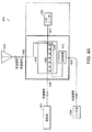
図5には、マッハツェンダ(MZ)干渉型変調器502を含む本発明の送受信兼用電気光学アンテナインターフェース500の一実施形態を示す。このアンテナインターフェース500は、光入力ポート504、光伝送信号入力ポート506、RF送受信兼用ポート508及び光出力ポート510を含む。アンテナ512はRF送受信兼用ポート508に電気的に接続されている。光伝送信号入力ポート506は、フォトダイオードのような光検出器514の入力端に光学的に結合されている。光検出器514の出力端はドライバ増幅器516の入力端515に電気的に接続されている。幾つかの実施形態では、RF伝送信号は、図5に点線により示すようにドライバ増幅器516の入力端515に直接に供給される。CWレーザ518は光入力ポート504へ光学的に結合されている。
FIG. 5 shows an embodiment of the transmission / reception combined use electro-
MZ変調器502は、光入力ポート504へ光学的に結合されている光入力端と、光出力ポート510へ光学的に結合されている光出力端とを有する。MZ変調器502は、進行波(TW)電極構造体518及び光導波路520を含む。ドライバ増幅器516の出力端はTW電極構造体518に電気的に接続されている。ドライバ増幅器516の出力インピーダンスはTW電極構造体518の一端を終端する。アンテナ512のインピーダンスはTW電極構造体518の他端を終端する。一実施形態では、MZ変調器502のTW電極構造体518は、受信信号をCW光ビームの光場と速度整合するように設計されている。速度整合は、MZ変調器502の帯域幅を維持しながら、MZ変調器の感度を改善できる。
一実施形態では、MZ変調器502のTW電極構造体518は比較的厚い。この実施形態では、TW電極構造体518の厚みは、過度の加熱損失または電気損失なしに、ドライバ増幅器516により増幅された信号を送信するのに充分であるように選択されている。一実施形態では、TW電極構造体518の厚みは、低いスイッチング電圧、従って、低いリンク雑音指数を達成するように選択されている。一実施形態では、電極構造体は、適度の(例えば、10ワットよりも少ない)送信電力で比較的低い損失を伴って比較的冷たい動作を行うように選択されている。このようなアンテナインターフェースは、典型的なフェイズドアレイの個々のアンテナ素子に対して充分である。
In one embodiment, the
動作中、受信信号はアンテナ512により受信され、次に、RF送受信兼用ポート508を通ってTW電極構造体518へ伝播する。この受信信号は次に、非可逆的にMZ変調器の光導波路520に伝播するCW光ビームに結合される。受信信号はCW光ビームに変調される。変調されたCW光ビームは、次に、光出力ポート510を通って伝播する。
In operation, the received signal is received by the
光ファイバ、導波路または自由空間に伝播する光伝送信号は光伝送信号入力ポート506により受信され、次に、光検出器514の入力端へ供給される。光検出器514はRF伝送信号を発生する。ドライバ増幅器516は、アンテナ512が放射するのに適するレベルまでRF伝送信号を増幅する。増幅された伝送信号は、速度整合方向と逆の方向へTW電極構造体518を通って伝播する。その結果として、アンテナインターフェース500の伝送信号は、光波を変調するのに比較的効率的ではない。しかし、変調効率の減少は、アンテナインターフェース500の送信−受信分離を増大させる。
The optical transmission signal propagating in the optical fiber, waveguide or free space is received by the optical transmission
送信−受信分離は幾つかのパラメータの関数である。送信−受信分離は伝播の方向の関数である。例えば、光信号と逆の方向へ伝播する電気信号に対するMZ変調器502の感度は、光信号の方向へ伝播する電気信号に対するMZ変調器502の感度よりも小さい。
Transmit-receive separation is a function of several parameters. Transmit-receive separation is a function of the direction of propagation. For example, the sensitivity of the
送信−受信分離はCW光信号の光電力の関数でもある。同時送受信が必要でない実施形態では、伝送中の光電力を減少させることにより送信−受信分離を増大できる。例えば、CWレーザ518が作動していないという制限では、送信−受信分離は無限である。従って、パルスによりCWレーザ518をオン及びオフすることにより、本発明のアンテナインターフェース500は、受信モードと送信モードとの間で理想的な(すなわち、オフモードで無限の分離を有する)電子切り換えの等価物を実装できる。
Transmit-receive separation is also a function of the optical power of the CW optical signal. In embodiments that do not require simultaneous transmission and reception, transmission-reception separation can be increased by reducing the optical power during transmission. For example, with the restriction that the
図6には、図5に関連して説明したレーザ518及びMZ変調器502と、pinフォトダイオード検出器とを含む受信リンクに対する平均リンク光検出器電流の関数として計算されたリンク雑音指数のグラフ600を示す。グラフは、変調器の様々な値Vπとレーザの相対強度雑音(RIN)とについて示す。
FIG. 6 shows a graph of link noise figure calculated as a function of average link photodetector current for a receive link including the
受信リンクの出力端に接続された光検出器が10mAよりも大きい電流を有する場合と、レーザの相対強度雑音(RIN)が充分に小さい場合とに、Vπ<0.3Vの要件を満たしている変調器が、5dBよりも小さい雑音指数を持つリンクを可能にすることをグラフ600は指摘している。このような変調器を本発明のアンテナインターフェースに用いることは、低い雑音指数のアンテナインターフェースをもたらす。従って、LNAの必要なしで、低い雑音指数を有するように本発明のアンテナインターフェースを構築できる。また、本発明のアンテナインターフェースは電子循環器を含まないので、電子循環器に起因する雑音指数のいかなる増大も存在しない。
When the photodetector connected to the output end of the receiving link has a current greater than 10 mA and when the relative intensity noise (RIN) of the laser is sufficiently small, the requirement of V π <0.3 V is satisfied.
比較的低い雑音指数の通信リンクを構築するのに本発明のアンテナインターフェースを用いることができる。本発明の電気光学送受信兼用アンテナインターフェースを用いる通信リンクには、3つの支配的な雑音源がある。第1の雑音源は、CWレーザ420(図4E)により発生された相対強度雑音(RIN)である。第2の雑音源は、終端インピーダンス464により発生された雑音である。第3の雑音源は、電気伝送線418により発生された熱雑音である。
The antenna interface of the present invention can be used to construct a relatively low noise figure communication link. There are three dominant noise sources in the communication link using the electro-optic transmitting / receiving antenna interface of the present invention. The first noise source is relative intensity noise (RIN) generated by the CW laser 420 (FIG. 4E). The second noise source is noise generated by the
固体レーザのように低いRINを有するレーザを選択することにより、CWレーザ420により発生されたRINを、無視できるレベルまで減少させることができる。アンテナインターフェースの所望の帯域幅内の最も低い周波数を超える周波数では、終端インピーダンス464により発生された雑音は重要でない。その理由は、光搬送波を変調するのに雑音は効力がないためである。終端インピーダンスにより発生された雑音が不整合方向へ伝播する(すなわち、速度整合方向と反対の方向へ伝播する)ので、効力のない変調が生じる。進行波電極で抵抗損により発生された熱雑音は、電極の長さに沿って統合される。
By selecting a laser with a low RIN, such as a solid state laser, the RIN generated by the
2dBよりも小さい雑音指数を有する広帯域低雑音増幅器は、市販されている。受動型光ファイバリンク(すなわち、能動型電子または光増幅器を用いないリンク)は、広帯域幅リンクに対して20〜30dB程度であるおそれがある比較的高い雑音指数を典型的に有する。変調器の集中定数電極のインピーダンスが入力インピーダンスに正確に整合すれば、受動型光リンク(すなわち、LNAを用いないリンク)に対する雑音指数限度は3dBに等しい。例えば、C.Cox氏等著,「Relationship Between Gain and Noise Figure of an Optical Analog Link」,カリフォルニア州サンフランシスコ,IEEE MTT−S Int.Microwave Symp.Dig.,1996年6月,p.1551〜1554を参照する。 Broadband low noise amplifiers with a noise figure smaller than 2 dB are commercially available. Passive fiber optic links (ie, links that do not use active electronic or optical amplifiers) typically have a relatively high noise figure that can be on the order of 20-30 dB for high bandwidth links. If the impedance of the modulator lumped electrode accurately matches the input impedance, the noise figure limit for a passive optical link (ie, a link without LNA) is equal to 3 dB. For example, C.I. Cox et al., “Relationship Between Gain and Noise Figure of an Optical Analog Link”, San Francisco, California, IEEE MTT-S Int. Microwave Symp. Dig. , June 1996, p. Reference is made to 1551-1554.
受動型光リンクで3dBより下に雑音指数を減少させるために雑音指数減少技術を用いることができる。例えば、発生源と変調器の集中定数電極構造体への入力との間のインピーダンス不整合を用いて雑音指数を減少させることができる。例えば、E.Ackerman氏等,「Input Impedance Conditions for Minimizing the Noise Figure of an Analog Optical Link」コロラド州デンバー,IEEE MTT−S Int.Microwave Symp.Dig.,1997年6月,p237〜240を参照する。この文書に記載された技術を用いて2.5dBの記録的な雑音指数を得た。 Noise figure reduction techniques can be used to reduce the noise figure below 3 dB in passive optical links. For example, an impedance mismatch between the source and the input to the modulator lumped electrode structure can be used to reduce the noise figure. For example, E.I. Ackerman et al., “Input Impedance Conditions for Minimizing the Noise Figure of an Analog Optical Link”, Denver, Colorado, IEEE MTT-S Int. Microwave Symp. Dig. , June 1997, p237-240. A record noise figure of 2.5 dB was obtained using the technique described in this document.
しかし、インピーダンス不整合技術は幾つかの制限を有する。例えば、インピーダンス不整合技術は、本質的に低周波数及び/または狭帯域幅技術である。その上、システムへ導入されたインピーダンス不整合は、不所望の副次的な悪影響を及ぼすおそれがある。例えば、インピーダンス不整合は、アンテナパターンの劣化を生じさせるおそれがある。 However, impedance mismatch techniques have some limitations. For example, impedance mismatch technology is essentially a low frequency and / or narrow bandwidth technology. Moreover, impedance mismatches introduced into the system can have undesirable side effects. For example, impedance mismatch may cause degradation of the antenna pattern.
進行波変調器を用いるリンクについて、リンク利得が充分に高く、レーザRINが充分に低い場合に達成できる雑音指数である最小達成可能な雑音指数を以下のように書くことができる。すなわち、
NFmin=10log[1+x]
ここで、xを、
For a link using a traveling wave modulator, the minimum achievable noise figure, which is the noise figure that can be achieved if the link gain is high enough and the laser RIN is low enough, can be written as: That is,
NF min = 10 log [1 + x]
Where x is

[sin(x)/x]2の項は、終端インピーダンスにより発生された逆伝播する雑音の影響を表す。残りの項は、単位長さα当たり幾らかのマイクロ波減衰をもたらす電極の抵抗損により発生された熱雑音の影響を表す。 The term [sin (x) / x] 2 represents the effect of backpropagating noise generated by the termination impedance. The remaining terms represent the effect of thermal noise generated by electrode resistance loss resulting in some microwave attenuation per unit length α.
図7A〜Cには、CWレーザと、進行波電極を有するMZ変調器と、pinフォトダイオード検出器とから成るリンクに対する計算された利得及び最小(すなわち、RIN=0)雑音指数データ対周波数のグラフ700を示す。このデータは、100MHzの周波数で30dBに等しいリンク利得を生じさせるVπの値及び平均光検出器電流を前提とする。2つの値の電極長さについて計算した結果をグラフ700に示す。2cmの電極に対するデータを点線により表し、4cmの電極長さに対するデータを破線で表す。すべてのグラフに対して、0.0015GHz−1cm−1に等しいとα1の値を仮定する。グラフ702は、0GHz−1/2cm−1に等しいα0に対するデータを表す。グラフ704は、α0=0.010GHz−1/2cm−1に対するデータを表す。グラフ706は、α0=0.043GHz−1/2cm−1に対するデータを表す。
7A-C shows the calculated gain and minimum (ie RIN = 0) noise figure data versus frequency for a link consisting of a CW laser, an MZ modulator with traveling wave electrodes, and a pin photodiode detector. A
グラフ702,704,706は、比較的広い帯域幅にわたって受動的に整合された光リンクに対して3dBの雑音指数限度を破ることができるということを指摘している。直感的には、この結果の理由は、送信−受信分離を行う同じ効果が、電気導波路418(図4E)の端部の終端インピーダンス464により発生された雑音からの分離をも行うということである。終端インピーダンス464により発生された雑音は典型的に、3dB雑音指数限度を生じさせる原因になっている。従って、終端インピーダンス464により発生された雑音の排除(または、少なくともかなりの減少)は、3dBよりも小さいリンク雑音指数を達成させることができる。
本発明の電気光学信号及びアンテナインターフェースは、多数の重要な特徴を有する。例えば、本発明のアンテナインターフェースはLNAを含まない。LNAを排除することは、非常に簡単なアンテナインターフェースをもたらし、高い送信電力により生じるおそれのある可能な増幅器被害を取り除く。また、本発明の電気光学アンテナインターフェースは電子循環器を含まない。電子循環器を排除することはインターフェースの重量を減少させ、送信−受信分離及び/または動作帯域幅を増大させることができる。 The electro-optic signal and antenna interface of the present invention has a number of important features. For example, the antenna interface of the present invention does not include an LNA. Eliminating the LNA provides a very simple antenna interface and removes possible amplifier damage that can be caused by high transmit power. The electro-optic antenna interface of the present invention does not include an electronic circulator. Eliminating electronic circulators can reduce the weight of the interface and increase transmit-receive separation and / or operating bandwidth.
更に、狭帯域または広帯域動作を行うように本発明の電気光学アンテナインターフェースを設計できる。また、本発明の電気光学アンテナインターフェースは、比較的低い雑音指数を有する受信機アンテナインターフェースを構成でき、適度な電力レベルを有する送信機インターフェースを構成できる。その上、本発明の電気光学アンテナインターフェースは、比較的低い損失と、高度な送信−受信分離とを有する。 Furthermore, the electro-optic antenna interface of the present invention can be designed to perform narrow band or wide band operation. Further, the electro-optic antenna interface of the present invention can constitute a receiver antenna interface having a relatively low noise figure, and can constitute a transmitter interface having an appropriate power level. Moreover, the electro-optic antenna interface of the present invention has relatively low loss and a high degree of transmit-receive separation.
本発明の信号及びアンテナインターフェースは、多数のその他の特徴を有する。例えば、本発明の信号及びアンテナインターフェースは、本明細書で記述したように本質的に広帯域であり、帯域幅を、比較的高い周波数まで延長できる。本発明の信号及びアンテナインターフェースは、本明細書で記述したように比較的小型、且つ、軽量でもある。例えば、アンテナ素子に物理的に装着すべき部品は変調器502及び送信ドライバ516だけである。より高い送信電力が要求されるならば、電力増幅器を含めることができる。遠く離れた位置にCWレーザ518を位置付けることができ、光ファイバを介してアンテナインターフェースへ結合できる。光ファイバを介してアンテナインターフェースへ伝送信号を結合すれば、アンテナインターフェースへの従来の電子供給を完全に排除できる。
The signal and antenna interface of the present invention has a number of other features. For example, the signal and antenna interface of the present invention is essentially broadband as described herein, and the bandwidth can be extended to relatively high frequencies. The signal and antenna interface of the present invention is also relatively small and lightweight as described herein. For example, the only components to be physically attached to the antenna element are the modulator 502 and the
本発明のアンテナインターフェースは多数の用途を有する。例えば、共形アンテナアレイ用の薄肉の開口アンテナに本発明のアンテナインターフェースを用いることができる。また、本発明のアンテナインターフェースは、比較的小型で、且つ、軽量であるので、空中及び人工衛星プラットフォームに特に適する。例えば、本発明のアンテナインターフェースを含む送信−受信モジュールの重量を、従来の送信/受信モジュールの重量の10%よりも少なくすることができる。 The antenna interface of the present invention has many uses. For example, the antenna interface of the present invention can be used for a thin-walled aperture antenna for a conformal antenna array. Also, the antenna interface of the present invention is particularly suitable for air and satellite platforms because it is relatively small and lightweight. For example, the weight of a transmit-receive module including the antenna interface of the present invention can be less than 10% of the weight of a conventional transmit / receive module.
(均等物)
特定の好適な実施形態に関して本発明を特に示し、説明したが、本明細書で規定した本発明の精神及び範囲から逸脱することなく、形態及び細部における様々な変更を行うことができることを当業者は理解すべきである。
(Equivalent)
While the invention has been particularly shown and described with respect to certain preferred embodiments, those skilled in the art will recognize that various changes in form and detail may be made without departing from the spirit and scope of the invention as defined herein. Should be understood.
Claims (28)
該受信されたRF受信信号を移す出力ポートに結合された一端と、レーザの出力部に結合された他端とを有し、第2の進行波を伝播する第2の導波路と、
該第1の導波路と該第2の導波路とを有する非可逆結合器と
を備えた送受信兼用信号インターフェースであって、
該非可逆結合器は、光学変調器であり、該非可逆結合器は、該第1の導波路からの電磁場が、該第1の導波路および該第2の導波路の長さに沿って連続した態様で該第2の導波路に結合されるように、該第1の導波路を該第2の導波路と近接するように位置付け、
該RF送受信兼用ポートからの該RF受信信号は、実質的に非可逆的に該第1の導波路から該第2の導波路へと結合し、該出力ポートを通過し、該RF入力ポートからの該RF伝送信号は、該第1の導波路を通過し該RF送受信兼用ポートに移る、信号インターフェース。A first traveling wave having one end coupled to an RF input port for receiving an RF transmission signal and another end coupled to an RF transmission / reception port for receiving the RF transmission signal and transmitting the RF transmission signal; A first waveguide propagating through
A second waveguide having one end coupled to the output port for transferring the received RF received signal and the other end coupled to the output of the laser and propagating a second traveling wave;
A transmission / reception signal interface comprising: a non-reciprocal coupler having the first waveguide and the second waveguide,
Continuous nonreciprocal coupler is an optical modulator, non-reversible coupler electromagnetic field from said first waveguide, along the length of said first waveguide and said second waveguide to be coupled to the second waveguide in the embodiment, positioned first waveguide so as to close and the second waveguide,
The RF received signal from the RF transceiver port is substantially irreversibly coupled from the first waveguide to the second waveguide, passed through the output port, and from the RF input port. The RF transmission signal of the signal passes through the first waveguide and moves to the RF transmission / reception port.
第1の導波路を介して第1の進行波を伝播し、第2の導波路を介して第2の進行波を伝播することと、
RF伝送信号の実質的な部分を該第2の導波路に結合せず、該第1の導波路を介して該RF伝送信号を送受信兼用ポートに伝播することと、
該送受信兼用ポートから該第1の導波路にRF受信信号を伝播することと、
該第1の導波路および該第2の導波路の長さに沿って連続した態様での該第1の導波路から該第2の導波路への該RF受信信号の結合が起こるように、該第1の導波路および該第2の導波路を互いに近接して配置することと、
該第2の導波路から出力ポートへと該RF受信信号を伝播することと
を包含する、方法。A method for interfacing a received signal and a transmitted signal,
Propagating a first traveling wave through a first waveguide and propagating a second traveling wave through a second waveguide;
Propagating the RF transmission signal to the transmit / receive port via the first waveguide without coupling a substantial portion of the RF transmission signal to the second waveguide;
Propagating an RF reception signal from the transmit / receive port to the first waveguide;
As binding of the RF signal received from the first waveguide in a state like that continuously along the length of the first waveguide and the second waveguide to the second waveguide occurs Placing the first waveguide and the second waveguide close to each other ;
Propagating the RF received signal from the second waveguide to an output port.
RF入力ポートにおいて前記RF伝送信号を受信することと、
光ビームを生成することと、
該RF受信信号を用いて該光ビームを変調し、該変調された光ビームを前記出力ポートへと移すことと、
該RF伝送信号を該RF送受信兼用ポートへと移すことと
をさらに包含する、請求項19〜23のいずれか一項に記載の方法。Receiving the RF reception signal at the RF transmission / reception port;
Receiving the RF transmission signal at an RF input port;
Generating a light beam;
Modulating the light beam with the RF received signal and transferring the modulated light beam to the output port;
The method according to any one of claims 19 to 23 , further comprising: transferring the RF transmission signal to the RF transmission / reception port.
Applications Claiming Priority (2)
| Application Number | Priority Date | Filing Date | Title |
|---|---|---|---|
| US48874803P | 2003-07-14 | 2003-07-14 | |
| PCT/US2004/022498 WO2005008832A2 (en) | 2003-07-14 | 2004-07-13 | Bi-directional signal interface |
Related Child Applications (1)
| Application Number | Title | Priority Date | Filing Date |
|---|---|---|---|
| JP2008301661A Division JP2009077428A (en) | 2003-07-14 | 2008-11-26 | Bi-directional signal interface |
Publications (2)
| Publication Number | Publication Date |
|---|---|
| JP2007532021A JP2007532021A (en) | 2007-11-08 |
| JP4478680B2 true JP4478680B2 (en) | 2010-06-09 |
Family
ID=34079452
Family Applications (2)
| Application Number | Title | Priority Date | Filing Date |
|---|---|---|---|
| JP2006520285A Expired - Fee Related JP4478680B2 (en) | 2003-07-14 | 2004-07-13 | Transmit / receive signal interface |
| JP2008301661A Pending JP2009077428A (en) | 2003-07-14 | 2008-11-26 | Bi-directional signal interface |
Family Applications After (1)
| Application Number | Title | Priority Date | Filing Date |
|---|---|---|---|
| JP2008301661A Pending JP2009077428A (en) | 2003-07-14 | 2008-11-26 | Bi-directional signal interface |
Country Status (8)
| Country | Link |
|---|---|
| US (3) | US7555219B2 (en) |
| EP (1) | EP1649539B1 (en) |
| JP (2) | JP4478680B2 (en) |
| KR (2) | KR100966222B1 (en) |
| CN (1) | CN1839511B (en) |
| AT (1) | ATE494643T1 (en) |
| DE (1) | DE602004030914D1 (en) |
| WO (1) | WO2005008832A2 (en) |
Cited By (6)
| Publication number | Priority date | Publication date | Assignee | Title |
|---|---|---|---|---|
| US9209840B2 (en) | 2012-07-30 | 2015-12-08 | Photonic Systems, Inc. | Same-aperture any-frequency simultaneous transmit and receive communication system |
| US9935680B2 (en) | 2012-07-30 | 2018-04-03 | Photonic Systems, Inc. | Same-aperture any-frequency simultaneous transmit and receive communication system |
| US10158432B2 (en) | 2015-10-22 | 2018-12-18 | Photonic Systems, Inc. | RF signal separation and suppression system and method |
| US10374656B2 (en) | 2012-07-30 | 2019-08-06 | Photonic Systems, Inc. | Same-aperture any-frequency simultaneous transmit and receive communication system |
| US10623986B2 (en) | 2015-10-22 | 2020-04-14 | Photonic Systems, Inc. | RF signal separation and suppression system and method |
| US11539392B2 (en) | 2012-07-30 | 2022-12-27 | Photonic Systems, Inc. | Same-aperture any-frequency simultaneous transmit and receive communication system |
Families Citing this family (45)
| Publication number | Priority date | Publication date | Assignee | Title |
|---|---|---|---|---|
| JP4478680B2 (en) | 2003-07-14 | 2010-06-09 | フォトニックシステムズ, インコーポレイテッド | Transmit / receive signal interface |
| US20050255812A1 (en) * | 2004-05-17 | 2005-11-17 | Samsung Electronics Co., Ltd. | RF front-end apparatus in a TDD wireless communication system |
| US20100117728A1 (en) * | 2005-03-10 | 2010-05-13 | Robert Ryan Riggsby | Signal Amplifiers Having Communications Paths that Automatically Terminate to a Matched Termination in Response to a Power Interruption and Related Methods |
| US7912431B2 (en) * | 2005-03-10 | 2011-03-22 | Commscope, Inc. Of North Carolina | Signal amplifiers having non-interruptible communication paths |
| US20060205442A1 (en) * | 2005-03-10 | 2006-09-14 | Neil Phillips | Bi-directional amplifier with non-interruptible port |
| US7809216B2 (en) | 2007-03-16 | 2010-10-05 | Photonic Systems, Inc. | Bi-directional signal interface and apparatus using same |
| JP4656156B2 (en) * | 2008-01-22 | 2011-03-23 | ソニー株式会社 | Optical communication device |
| US8433163B2 (en) * | 2008-04-21 | 2013-04-30 | Photonic Systems, Inc | Bi-directional signal interface with enhanced isolation |
| US8682170B2 (en) | 2011-05-20 | 2014-03-25 | The Trustees Of Princeton University | System and method for broadband RF interference cancellation |
| US8693810B2 (en) | 2008-11-05 | 2014-04-08 | The Trustees Of Princeton University | Optical counter-phase system and method of RF interference cancellation |
| JP5446552B2 (en) * | 2009-07-30 | 2014-03-19 | ソニー株式会社 | Wireless communication device, rotating structure, electronic device |
| JP5398553B2 (en) * | 2010-01-06 | 2014-01-29 | 三菱電機株式会社 | Optical transmission equipment for radio wave systems |
| US8755750B2 (en) | 2010-05-22 | 2014-06-17 | Photonic Systems, Inc. | Wide-bandwidth signal canceller |
| US8124505B1 (en) | 2010-10-21 | 2012-02-28 | Hrl Laboratories, Llc | Two stage plasma etching method for enhancement mode GaN HFET |
| US8853709B2 (en) | 2011-07-29 | 2014-10-07 | Hrl Laboratories, Llc | III-nitride metal insulator semiconductor field effect transistor |
| US9335568B1 (en) | 2011-06-02 | 2016-05-10 | Hrl Laboratories, Llc | Electro-optic grating modulator |
| US9250452B1 (en) | 2011-10-13 | 2016-02-02 | Hrl Laboratories, Llc | Tunable photonic RF circulator for simultaneous transmit and receive |
| US9337332B2 (en) | 2012-04-25 | 2016-05-10 | Hrl Laboratories, Llc | III-Nitride insulating-gate transistors with passivation |
| US20140349584A1 (en) * | 2013-05-24 | 2014-11-27 | Thorsten Clevorn | Communication device and method for performing radio communication |
| CN105556678B (en) | 2013-09-30 | 2018-04-10 | Hrl实验室有限责任公司 | normally-off III-nitride transistor with high threshold voltage and low on-resistance |
| US9699516B2 (en) | 2014-01-21 | 2017-07-04 | Commscope, Inc. Of North Carolina | Signal amplifiers that support MoCA communications at both active and passive output ports |
| US9240842B2 (en) | 2014-03-24 | 2016-01-19 | The United States Of America As Represented By The Secretary Of The Air Force | Isolation of RF signals using optical single side band modulation combined with optical filtering |
| US10276712B2 (en) | 2014-05-29 | 2019-04-30 | Hrl Laboratories, Llc | III-nitride field-effect transistor with dual gates |
| US10090585B2 (en) | 2015-08-23 | 2018-10-02 | The Trustees Of Columbia University In The City Of New York | Circuits and methods for antenna-based self-interference cancellation |
| US9812532B1 (en) | 2015-08-28 | 2017-11-07 | Hrl Laboratories, Llc | III-nitride P-channel transistor |
| US9780943B2 (en) | 2015-11-13 | 2017-10-03 | Northrop Grumman Systems Corporation | Broadband distributed amplifier based active duplexer |
| EP3378097A4 (en) | 2015-11-19 | 2019-09-11 | HRL Laboratories, LLC | Iii-nitride field-effect transistor with dual gates |
| US10581135B2 (en) | 2015-12-07 | 2020-03-03 | The Trustees Of Columbia University In The City Of New York | Circuits and methods for non-reciprocal circulators and transceivers using same |
| US9887862B2 (en) * | 2015-12-07 | 2018-02-06 | The Trustees Of Columbia University In The City Of New York | Circuits and methods for performing self-interference cancelation in full-duplex transceivers |
| US9735854B2 (en) * | 2016-01-18 | 2017-08-15 | Qorvo Us, Inc. | Systems for antenna swapping switching and methods of operation thereof |
| US9692469B1 (en) | 2016-02-23 | 2017-06-27 | Resonant Sciences, LLC | Interference signal cancellation over a broad frequency range |
| US9882654B1 (en) * | 2016-03-17 | 2018-01-30 | Hrl Laboratories, Llc | Jammer-suppressed photonic-enabled RF link |
| US9793972B1 (en) | 2016-04-04 | 2017-10-17 | Qorvo Us, Inc. | Multiple-input multiple-output (MIMO) antenna swapping circuit |
| CN106059617B (en) * | 2016-07-15 | 2019-02-01 | 上海捷士太通讯技术有限公司 | A kind of antenna integrated Universal wireless communication module |
| EP3488500A4 (en) | 2016-07-21 | 2020-04-15 | Tolga Dinc | Magnetic-free non-reciprocal circuits based on sub-harmonic spatio-temporal conductance modulation |
| US9960849B1 (en) * | 2016-12-22 | 2018-05-01 | Intel Corporation | Channelization for dispersion limited waveguide communication channels |
| US10355771B1 (en) | 2017-05-22 | 2019-07-16 | Resonant Sciences, LLC | RF repeater and mobile unit with cancellation of interference from a repeated signal |
| WO2019067294A1 (en) | 2017-09-26 | 2019-04-04 | Photonic Systems, Inc | Single-channel, full-time full-duplex wireless signal transmission system |
| US11349569B2 (en) * | 2018-10-26 | 2022-05-31 | Raytheon Company | Methods and apparatus for implementing an optical transceiver using a vapor cell |
| WO2020132611A1 (en) * | 2018-12-20 | 2020-06-25 | California Institute Of Technology | Spatial redistributors and methods of redistributing mm-wave signals |
| US11307395B2 (en) | 2019-05-23 | 2022-04-19 | Raytheon Company | Methods and apparatus for optical path length equalization in an optical cavity |
| WO2020256823A1 (en) | 2019-06-20 | 2020-12-24 | Raytheon Company | Methods and apparatus for tracking moving objects using symmetric phase change detection |
| EP3994808A1 (en) | 2019-07-03 | 2022-05-11 | Raytheon Company | Optical receiver comprising a rotatable optical resonator, and method for demodulating an optical signal using said receiver |
| US11199754B2 (en) | 2019-07-15 | 2021-12-14 | Raytheon Company | Demodulator with optical resonator |
| US20220140911A1 (en) * | 2020-10-31 | 2022-05-05 | Photonic Systems, Inc. | Bi-directional signal interface with suppression of reflected signals |
Family Cites Families (45)
| Publication number | Priority date | Publication date | Assignee | Title |
|---|---|---|---|---|
| GB848113A (en) * | 1957-08-20 | 1960-09-14 | Gen Electric Co Ltd | Improvements in or relating to electromagnetic wave switching arrangements |
| US5010342A (en) * | 1973-05-14 | 1991-04-23 | Jones Jr James R | Radar simulator |
| JPS57197934A (en) | 1981-05-29 | 1982-12-04 | Fujitsu Ten Ltd | Radio transmitter and receiver |
| FR2574943B1 (en) * | 1984-12-18 | 1987-05-22 | Thomson Csf | TRANSIENT ANALYZER SYSTEM |
| GB2181007A (en) * | 1985-09-27 | 1987-04-08 | Philips Electronic Associated | Distributed amplifier load arrangements |
| JPH0750265B2 (en) * | 1986-08-20 | 1995-05-31 | 川上 彰二郎 | Wideband traveling waveform optical modulator |
| US4801901A (en) * | 1987-03-13 | 1989-01-31 | Hittite Microwave Corporation | Non-ferrite non-reciprocal phase shifter and circulator |
| CA2011954C (en) | 1989-03-14 | 1994-02-22 | Hiroshi Hamano | Optical modulator |
| US4908820A (en) * | 1989-03-29 | 1990-03-13 | Hittite Microwave Corporation | Non-reciprocal bidirectional duplexer |
| US5287212A (en) | 1989-09-07 | 1994-02-15 | Cox Charles H | Optical link |
| US5105166A (en) * | 1989-11-30 | 1992-04-14 | Raytheon Company | Symmetric bi-directional amplifier |
| EP0430509A3 (en) * | 1989-11-30 | 1991-11-06 | Raytheon Company | Symmetric bi-directional amplifier |
| DE69113116T2 (en) * | 1990-05-29 | 1996-04-18 | Philips Electronics Nv | Slow-wave microstrip transmission line and arrangement with such a line. |
| JPH0773247B2 (en) * | 1991-03-08 | 1995-08-02 | 株式会社エイ・ティ・アール光電波通信研究所 | Optical transmission system for antenna feeding |
| US5309532A (en) * | 1991-12-02 | 1994-05-03 | The Regents Of The University Of California | Electro-optic intensity modulator with improved linearity |
| US5303079A (en) * | 1992-04-09 | 1994-04-12 | At&T Bell Laboratories | Tunable chirp, lightwave modulator for dispersion compensation |
| US6337660B1 (en) | 1993-09-17 | 2002-01-08 | The United States Of America As Represented By The Secretary Of The Navy | Fiber optic true time-delay array antenna feed system |
| US5389782A (en) * | 1994-05-13 | 1995-02-14 | The United States Of America As Represented By The Secretary Of The Navy | Optically powered amplifier used by an electromagnetic field sensor to amplify an electrical signal from an antenna |
| JPH098737A (en) | 1995-06-23 | 1997-01-10 | Tokin Corp | Reception system |
| US5602387A (en) * | 1995-06-26 | 1997-02-11 | The United States Of America As Represented By The Secretary Of The Air Force | Method of protecting an RF receiver in a hostile electromagnetic environment |
| US6525855B1 (en) * | 1996-07-19 | 2003-02-25 | British Telecommunications Public Limited Company | Telecommunications system simultaneously receiving and modulating an optical signal |
| DE19649085A1 (en) | 1996-11-27 | 1998-05-28 | Alsthom Cge Alcatel | Transmitting / receiving device and method for transmitting broadband signals and transmitting / receiving device for receiving broadband signals |
| US5977911A (en) | 1996-12-30 | 1999-11-02 | Raytheon Company | Reactive combiner for active array radar system |
| US6295395B1 (en) | 1997-01-31 | 2001-09-25 | The United States Of America As Represented By The Secretary Of Commerce | True time delay generation utilizing broadband light source with fiber chirp grating array and acousto-optic beam steering and 2-D architectures |
| JPH1152313A (en) | 1997-08-08 | 1999-02-26 | Mitsubishi Electric Corp | Optical modulation device |
| CN1302388A (en) * | 1997-08-18 | 2001-07-04 | 皮雷利·卡维系统有限公司 | Narrow band optical modulator with reduced power requirement |
| JP3959797B2 (en) * | 1997-09-17 | 2007-08-15 | 有限会社ケイラボラトリー | Lumped constant circulator |
| US6393177B2 (en) | 1998-01-20 | 2002-05-21 | United States Of America | True time delay generating system and method |
| US6137442A (en) | 1998-04-01 | 2000-10-24 | The United States Of America As Represented By The Secretary Of The Navy | Chirped fiber grating beamformer for phased array antennas |
| US6081232A (en) | 1998-07-06 | 2000-06-27 | The United States Of America As Represented By The Secretary Of The Army | Communication relay and a space-fed phased array radar, both utilizing improved mach-zehnder interferometer |
| US6175672B1 (en) | 1999-06-18 | 2001-01-16 | Raytheon Company | RF wide bandwidth lossless high performance low noise transmissive link |
| JP2001036169A (en) | 1999-07-23 | 2001-02-09 | Furukawa Electric Co Ltd:The | Bilateral pumping light amplifier |
| US6330098B1 (en) | 1999-10-06 | 2001-12-11 | Codeon Corporation | Apparatus for externally modulating two optical channels at the same time |
| US6320539B1 (en) | 2000-06-09 | 2001-11-20 | The United States Of America As Represented By The Secretary Of The Navy | Fiber-optic, wideband array antenna beamformer |
| US20020106141A1 (en) * | 2001-02-08 | 2002-08-08 | Codeon Corporation | Low-loss electrode designs for high-speed optical modulators |
| US6580843B2 (en) | 2001-04-05 | 2003-06-17 | Fujitsu Limited | Optical device |
| JPWO2002097521A1 (en) * | 2001-05-25 | 2004-09-16 | アンリツ株式会社 | Optical modulation device having excellent electrical characteristics by effectively suppressing thermal drift and method of manufacturing the same |
| JP3885528B2 (en) * | 2001-07-04 | 2007-02-21 | 株式会社日立製作所 | Light modulator |
| JP2003262841A (en) * | 2002-03-07 | 2003-09-19 | Fujitsu Ltd | Optical modulator and designing method |
| US6873750B2 (en) * | 2002-03-13 | 2005-03-29 | Telecommunications Research Laboratories | Electro-optic modulator with resonator |
| JP3936256B2 (en) * | 2002-07-18 | 2007-06-27 | 富士通株式会社 | Optical semiconductor device |
| JP3957217B2 (en) * | 2002-12-06 | 2007-08-15 | 富士通株式会社 | Light modulator |
| US7042305B2 (en) * | 2002-12-20 | 2006-05-09 | Com Dev Ltd. | Transmission line termination |
| JP4478680B2 (en) | 2003-07-14 | 2010-06-09 | フォトニックシステムズ, インコーポレイテッド | Transmit / receive signal interface |
| US7561803B2 (en) * | 2006-02-14 | 2009-07-14 | Photonic Systems, Inc. | Bi-directional signal interface using photonic coupler |
-
2004
- 2004-07-13 JP JP2006520285A patent/JP4478680B2/en not_active Expired - Fee Related
- 2004-07-13 EP EP04778144A patent/EP1649539B1/en not_active Not-in-force
- 2004-07-13 KR KR1020067000872A patent/KR100966222B1/en active IP Right Grant
- 2004-07-13 US US10/710,463 patent/US7555219B2/en active Active
- 2004-07-13 WO PCT/US2004/022498 patent/WO2005008832A2/en active Application Filing
- 2004-07-13 CN CN2004800236254A patent/CN1839511B/en not_active Expired - Fee Related
- 2004-07-13 KR KR1020097014602A patent/KR101222726B1/en active IP Right Grant
- 2004-07-13 DE DE602004030914T patent/DE602004030914D1/en active Active
- 2004-07-13 AT AT04778144T patent/ATE494643T1/en not_active IP Right Cessation
-
2008
- 2008-11-26 JP JP2008301661A patent/JP2009077428A/en active Pending
-
2009
- 2009-05-22 US US12/471,312 patent/US8868006B2/en active Active
- 2009-06-12 US US12/483,962 patent/US7826751B2/en active Active
Cited By (9)
| Publication number | Priority date | Publication date | Assignee | Title |
|---|---|---|---|---|
| US9209840B2 (en) | 2012-07-30 | 2015-12-08 | Photonic Systems, Inc. | Same-aperture any-frequency simultaneous transmit and receive communication system |
| US9935680B2 (en) | 2012-07-30 | 2018-04-03 | Photonic Systems, Inc. | Same-aperture any-frequency simultaneous transmit and receive communication system |
| US10374656B2 (en) | 2012-07-30 | 2019-08-06 | Photonic Systems, Inc. | Same-aperture any-frequency simultaneous transmit and receive communication system |
| US10425121B2 (en) | 2012-07-30 | 2019-09-24 | Photonic Systems, Inc. | Same-aperture any-frequency simultaneous transmit and receive communication system |
| US10651886B2 (en) | 2012-07-30 | 2020-05-12 | Photonic Systems, Inc. | Same-aperture any-frequency simultaneous transmit and receive communication system |
| US10879950B2 (en) | 2012-07-30 | 2020-12-29 | Photonic Systems, Inc. | Same-aperture any-frequency simultaneous transmit and receive communication system |
| US11539392B2 (en) | 2012-07-30 | 2022-12-27 | Photonic Systems, Inc. | Same-aperture any-frequency simultaneous transmit and receive communication system |
| US10158432B2 (en) | 2015-10-22 | 2018-12-18 | Photonic Systems, Inc. | RF signal separation and suppression system and method |
| US10623986B2 (en) | 2015-10-22 | 2020-04-14 | Photonic Systems, Inc. | RF signal separation and suppression system and method |
Also Published As
| Publication number | Publication date |
|---|---|
| EP1649539A2 (en) | 2006-04-26 |
| US7826751B2 (en) | 2010-11-02 |
| KR101222726B1 (en) | 2013-01-15 |
| DE602004030914D1 (en) | 2011-02-17 |
| JP2009077428A (en) | 2009-04-09 |
| WO2005008832A2 (en) | 2005-01-27 |
| KR100966222B1 (en) | 2010-07-01 |
| CN1839511A (en) | 2006-09-27 |
| US7555219B2 (en) | 2009-06-30 |
| US20050014472A1 (en) | 2005-01-20 |
| WO2005008832A3 (en) | 2005-03-24 |
| CN1839511B (en) | 2012-07-18 |
| US20090274466A1 (en) | 2009-11-05 |
| EP1649539B1 (en) | 2011-01-05 |
| KR20090088456A (en) | 2009-08-19 |
| US8868006B2 (en) | 2014-10-21 |
| US20090247074A1 (en) | 2009-10-01 |
| ATE494643T1 (en) | 2011-01-15 |
| JP2007532021A (en) | 2007-11-08 |
| KR20060037350A (en) | 2006-05-03 |
Similar Documents
| Publication | Publication Date | Title |
|---|---|---|
| JP4478680B2 (en) | Transmit / receive signal interface | |
| US7561803B2 (en) | Bi-directional signal interface using photonic coupler | |
| EP2132594B1 (en) | Bi-directional signal interface and apparatus using same | |
| JP2009077428A5 (en) | ||
| CN111431622B (en) | Photoelectric fusion continuous wave radar leakage interference elimination device and method | |
| US5109449A (en) | Variable optical fiber delay line | |
| JP2807651B2 (en) | Semiconductor electro-absorption optical modulator | |
| Meyer | Using fiber optics with analog RF signals | |
| JPH0354494B2 (en) | ||
| US3027453A (en) | Electrical duplexer employing a traveling wave tube as a directional coupler | |
| KR100743425B1 (en) | Rf front-end apparatus in tdd wireless communication system | |
| US20220140911A1 (en) | Bi-directional signal interface with suppression of reflected signals | |
| Stephens et al. | RF Fiber Optic Links for Avionics Applications | |
| Iwashita et al. | 4Gbit/s CPFSK transmission experiment through 155km single-mode fiber | |
| KR100759271B1 (en) | Optical transceiver which is used in rof communication system | |
| KR100906776B1 (en) | Interference suppress system filter module having switching low noise amplifier | |
| Johnson et al. | Components and applications for high-speed optical analog links | |
| JPH10186189A (en) | Transmission system with reception part | |
| CN114879387A (en) | Lithium niobate intensity modulator and optical transceiver module | |
| US7589887B2 (en) | Low loss fiber optic link using an optical amplifier | |
| JPH02281205A (en) | Variable optical fiber delay line | |
| CN116074175A (en) | Active backscattering 2ASK modulating device | |
| Bruno et al. | Rf Fiber Optic Links For Spacecraft And Aircraft Applications | |
| JPH10190587A (en) | Transmission/reception system | |
| Gosling | Radio frequency engineering: opportunity and challenge |
Legal Events
| Date | Code | Title | Description |
|---|---|---|---|
| A131 | Notification of reasons for refusal |
Free format text: JAPANESE INTERMEDIATE CODE: A131 Effective date: 20080827 |
|
| A521 | Request for written amendment filed |
Free format text: JAPANESE INTERMEDIATE CODE: A523 Effective date: 20081126 |
|
| A131 | Notification of reasons for refusal |
Free format text: JAPANESE INTERMEDIATE CODE: A131 Effective date: 20081219 |
|
| A601 | Written request for extension of time |
Free format text: JAPANESE INTERMEDIATE CODE: A601 Effective date: 20090310 |
|
| A602 | Written permission of extension of time |
Free format text: JAPANESE INTERMEDIATE CODE: A602 Effective date: 20090317 |
|
| A601 | Written request for extension of time |
Free format text: JAPANESE INTERMEDIATE CODE: A601 Effective date: 20090513 |
|
| A602 | Written permission of extension of time |
Free format text: JAPANESE INTERMEDIATE CODE: A602 Effective date: 20090520 |
|
| A521 | Request for written amendment filed |
Free format text: JAPANESE INTERMEDIATE CODE: A523 Effective date: 20090619 |
|
| TRDD | Decision of grant or rejection written | ||
| A01 | Written decision to grant a patent or to grant a registration (utility model) |
Free format text: JAPANESE INTERMEDIATE CODE: A01 Effective date: 20100215 |
|
| A01 | Written decision to grant a patent or to grant a registration (utility model) |
Free format text: JAPANESE INTERMEDIATE CODE: A01 |
|
| A61 | First payment of annual fees (during grant procedure) |
Free format text: JAPANESE INTERMEDIATE CODE: A61 Effective date: 20100315 |
|
| R150 | Certificate of patent or registration of utility model |
Ref document number: 4478680 Country of ref document: JP Free format text: JAPANESE INTERMEDIATE CODE: R150 Free format text: JAPANESE INTERMEDIATE CODE: R150 |
|
| FPAY | Renewal fee payment (event date is renewal date of database) |
Free format text: PAYMENT UNTIL: 20130319 Year of fee payment: 3 |
|
| FPAY | Renewal fee payment (event date is renewal date of database) |
Free format text: PAYMENT UNTIL: 20140319 Year of fee payment: 4 |
|
| R250 | Receipt of annual fees |
Free format text: JAPANESE INTERMEDIATE CODE: R250 |
|
| R250 | Receipt of annual fees |
Free format text: JAPANESE INTERMEDIATE CODE: R250 |
|
| R250 | Receipt of annual fees |
Free format text: JAPANESE INTERMEDIATE CODE: R250 |
|
| R250 | Receipt of annual fees |
Free format text: JAPANESE INTERMEDIATE CODE: R250 |
|
| R250 | Receipt of annual fees |
Free format text: JAPANESE INTERMEDIATE CODE: R250 |
|
| R250 | Receipt of annual fees |
Free format text: JAPANESE INTERMEDIATE CODE: R250 |
|
| LAPS | Cancellation because of no payment of annual fees |