JP4439154B2 - Method and apparatus for interleaved non-blocking packet buffer - Google Patents
Method and apparatus for interleaved non-blocking packet buffer Download PDFInfo
- Publication number
- JP4439154B2 JP4439154B2 JP2001521004A JP2001521004A JP4439154B2 JP 4439154 B2 JP4439154 B2 JP 4439154B2 JP 2001521004 A JP2001521004 A JP 2001521004A JP 2001521004 A JP2001521004 A JP 2001521004A JP 4439154 B2 JP4439154 B2 JP 4439154B2
- Authority
- JP
- Japan
- Prior art keywords
- memory
- address
- write
- port
- read
- Prior art date
- Legal status (The legal status is an assumption and is not a legal conclusion. Google has not performed a legal analysis and makes no representation as to the accuracy of the status listed.)
- Expired - Fee Related
Links
Images


Classifications
-
- G—PHYSICS
- G06—COMPUTING; CALCULATING OR COUNTING
- G06F—ELECTRIC DIGITAL DATA PROCESSING
- G06F12/00—Accessing, addressing or allocating within memory systems or architectures
- G06F12/02—Addressing or allocation; Relocation
- G06F12/06—Addressing a physical block of locations, e.g. base addressing, module addressing, memory dedication
- G06F12/0607—Interleaved addressing
-
- H—ELECTRICITY
- H04—ELECTRIC COMMUNICATION TECHNIQUE
- H04L—TRANSMISSION OF DIGITAL INFORMATION, e.g. TELEGRAPHIC COMMUNICATION
- H04L49/00—Packet switching elements
- H04L49/10—Packet switching elements characterised by the switching fabric construction
- H04L49/103—Packet switching elements characterised by the switching fabric construction using a shared central buffer; using a shared memory
-
- H—ELECTRICITY
- H04—ELECTRIC COMMUNICATION TECHNIQUE
- H04L—TRANSMISSION OF DIGITAL INFORMATION, e.g. TELEGRAPHIC COMMUNICATION
- H04L49/00—Packet switching elements
- H04L49/90—Buffering arrangements
-
- H—ELECTRICITY
- H04—ELECTRIC COMMUNICATION TECHNIQUE
- H04L—TRANSMISSION OF DIGITAL INFORMATION, e.g. TELEGRAPHIC COMMUNICATION
- H04L49/00—Packet switching elements
- H04L49/90—Buffering arrangements
- H04L49/9036—Common buffer combined with individual queues
-
- H—ELECTRICITY
- H04—ELECTRIC COMMUNICATION TECHNIQUE
- H04L—TRANSMISSION OF DIGITAL INFORMATION, e.g. TELEGRAPHIC COMMUNICATION
- H04L49/00—Packet switching elements
- H04L49/90—Buffering arrangements
- H04L49/9084—Reactions to storage capacity overflow
- H04L49/9089—Reactions to storage capacity overflow replacing packets in a storage arrangement, e.g. pushout
-
- H—ELECTRICITY
- H04—ELECTRIC COMMUNICATION TECHNIQUE
- H04L—TRANSMISSION OF DIGITAL INFORMATION, e.g. TELEGRAPHIC COMMUNICATION
- H04L49/00—Packet switching elements
- H04L49/15—Interconnection of switching modules
- H04L49/1515—Non-blocking multistage, e.g. Clos
- H04L49/1546—Non-blocking multistage, e.g. Clos using pipelined operation
Landscapes
- Engineering & Computer Science (AREA)
- Computer Networks & Wireless Communication (AREA)
- Signal Processing (AREA)
- Theoretical Computer Science (AREA)
- Physics & Mathematics (AREA)
- General Engineering & Computer Science (AREA)
- General Physics & Mathematics (AREA)
- Data Exchanges In Wide-Area Networks (AREA)
Description
【0001】
【発明の背景】
ネットワークスイッチは、スイッチに接続されたいくつかの入力ポートからデータパケットを受取り、データパケットをスイッチに接続されたいくつかの出力ポートに与える。スイッチは、データパケットに含まれるデスティネーションアドレスに依存して、データパケットを与えるべき出力ポートを判断する。入力ポートから受取られたデータパケットは、出力ポートに与えられる前にスイッチ内のメモリに記憶される。
【0002】
スイッチ内のメモリは、すべての入力ポートから受取られたすべてのデータパケットが出力ポートに与えられる前に記憶される共通メモリであり得る。非ブロッキングスイッチは、すべての入力ポートで受取られたすべてのデータが、出力ポートに与えられることを可能にする。非ブロッキングスイッチは、典型的にはポートごとに最大量のメモリを利用可能にするための共通メモリを含む。
【0003】
共通メモリスイッチの速度は、メモリバンド幅に依存する。メモリバンド幅はメモリアクセスタイムおよびメモリの幅に依存するが、これはすなわち、メモリアクセス時間ごとにアクセスされるバイトの数である。たとえば、もし共通メモリが64バイト幅であり、かつ80ナノ秒(ns)のアクセス時間を有していれば、64バイトを書込または読出するために80nsかかる。スイッチに接続される入力ポートが100メガビット(M)bps(秒当たりのビット)でデータを受取ると、1ビットは10nsごとに受取られ、8ビットバイトは80nsごとに受取られ、かつ64バイトは5120nsごとに受取られる。64バイトのデータが受取られた後で、書込メモリサイクルが行なわれて64バイト幅メモリへの単一のアクセスで64バイトを書込む。入力ポートは、5120nsごとにメモリバンド幅を80ns使用して、受取ったデータをメモリに書込む。こうして、80nsのアクセス時間を備えた64バイト幅メモリは、64(5120ns/80ns)の100Mbpsのポートをサポートできる。64ポートがスイッチに接続されていると、各ポートサイクルは80nsである。80nsポートサイクルは、各ポートに、ポートサイクルごとに1つのメモリアクセスを提供する。
【0004】
各ポートサイクルで利用可能であるメモリバンド幅を増大させると、以下のうちの1つ以上が必要となる:メモリアクセス時間の減少、メモリの幅(すなわち、メモリサイクルごとに読出/書込されるビット数)の増大、または、ポートの数の減少。メモリの幅の増大は、最小データパケットサイズによって制限される。メモリアクセス時間の減少は、メモリに対する最小メモリアクセス時間によって制限される。
【0005】
メモリバンド幅は、たとえば第1のデータパケットを第1のメモリバンクに書込み、第2のデータパケットを第2のデータバンクに書込むためのメモリバンクをインターリーブさせることによっても増大させることができる。しかしながら、スイッチ内のデータをインターリーブさせると、たとえばもしポートAおよびポートBの両方が同時に第1のメモリバンクへのアクセスを要求している場合、ブロッキングをまねくおそれがある。入力ポートと出力ポートとの間でのデータ転送のブロッキングは、パケットの脱落をもたらすおそれがある。よって、非ブロッキングスイッチにおいては、メモリバンド幅を増大させるために用いることはできない。
【0006】
【発明の要約】
スイッチにおけるパケットストレージマネージャは、スイッチに接続される入力ポートおよび出力ポートによって共有されるメモリのメモリバンド幅を増大させる。パケットストレージマネージャは、先行技術のシステムが逐次的な読出および書込サイクルを必要としたところを、単一のポートサイクルで、入力ポートのうちの1つに対する書込動作および出力ポートのうちの1つに対する読出動作の両方を行なう。書込および読出動作は、単一のメモリアクセスサイクルにおいて、メモリ内の異なったメモリに対して並行に行なわれる。メモリは、物理的にいくつかのバンクに分割される。バンクの数は、好ましくは2つまたは4つである。読出および書込動作は異なったバンクに対して行なわれる。
【0007】
パケットストレージマネージャは、ポートサイクルに依存して読出動作のためにメモリにおける読出アドレスを選択する読出アドレス論理と、読出アドレス論理によって選択された読出アドレスに依存して、書込動作のための書込アドレスを選択する書込アドレス論理とを含む。書込アドレスは、読出アドレスに依存して書込アドレスを選択して、読出および書込動作が単一のメモリアクセスで並行して行なわれるようにする。パケットストレージマネージャは、出力ポートごとのポート待ち行列と、ポート待ち行列には記憶されていないアドレスの空きリストとに依拠する。入来するパケットから、マネージャはネットワークデスティネーションを読出し、パケットが記憶されるべき適切な出力ポートを判断する。マネージャは、空きリストからメモリセグメントアドレスを除去することによりパケットセグメントをメモリに書込み、パケットが向けられるべき各ポート待ち行列の最後にセグメントアドレスを記憶し、セグメントアドレスによって特定されるメモリ内の場所にパケットセグメントを書込む。同時に、各ポート待ち行列の先頭でのアドレスは、マネージャによって読出されるべきパケットセグメントを識別する。
【0008】
パケットストレージマネージャ内の読出アドレス論理は、各出力ポートに対するポート待ち行列を含む。ポート待ち行列は、各入力ポートによってメモリに書込まれるデータのメモリ場所を記憶する。ポート待ち行列選択論理は、ポートサイクルに依存して、メモリアドレスが除去されるべきポート待ち行列を選択する。読出選択論理は、ポート待ち行列から除去されたメモリアドレスに依存して、読出されるべきメモリ場所を選択する。
【0009】
メモリは物理的にいくつかのバンクに分割される。バンクの数は好ましくは2つまたは4つである。パケットストレージマネージャ内の書込アドレス論理は、バンクごとのバンク空きリストを含む。各バンク空きリストは、メモリのバンク内の利用可能な場所のアドレスを記憶する。書込アドレス論理内の書込選択論理は、書込アドレスを除去すべきバンク空きリストのうちの1つを選択する。書込選択論理は、バンク空きリストを選択して、それによりデータパケットの順次的セグメントが、メモリの交互の奇数および偶数バンクに書込まれるようにする。
【0010】
書込アドレス論理はまた、バンクごとのバンク空きリストカウンタを含む。バンク空きリストカウンタは、バンク内の利用可能な場所のカウントを記憶する。書込選択論理は、バンク空きリストカウンタにおけるカウントに依存して、バンク空きリストを選択し得る。並行的な読出および書込動作は、同じポートに対するものであっても、または異なったポートに対するものであってもよい。
【0011】
上述の目的ならびに他の目的、およびこの発明の特徴ならびに利点は、添付の図面に示されるこの発明の好ましい実施例のより特定的な説明から明らかとなるであろうが、図面においては同様の要素には同様の参照符号が異なる図面を通して付与される。図面は必ずしも実物と同じスケールである必要はなく、この発明の原理を例示することが重視される。
【0012】
【発明の説明】
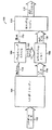
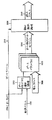
図1Aは、共通メモリスイッチ100のブロック図である。入力ポート102で受取られたすべてのデータは、セグメントバッファメモリ108に記憶されて、その後1つ以上の出力ポート112にスイッチされる。パケットストレージマネージャ106は、セグメントバッファメモリ108に対する書込および読出アクセスを制御する。パケットストレージマネージャ106を介して、入力ポート102に到着するデータパケットセグメントはセグメントバッファメモリ108に書込まれ、同じメモリアクセスサイクルにおいて、出力ポート112に対する別のデータパケットセグメントがセグメントバッファメモリ108から読出される。
【0013】
スイッチ100は、入力ポートエンジン104および出力ポートエンジン110を含む。データパケットは入力ポート102で順次的に受取られる。入力エンジン104は、受取ったデータパケット内のヘッダを検出して処理し、検出したヘッダからどの出力ポート112にデータパケットを転送するべきかを判断し、データパケットに対する転送ベクトル114を生成する。転送ベクトル114はビットマップであり、1つのビットが複数の出力ポート112の各々に対応し、データパケットがその出力ポート112に転送されるべきどうかを示す。転送ベクトル114は、パケットストレージマネージャ106に転送される。
【0014】
パケットストレージマネージャ106は、セグメントバッファメモリ108へのアクセスを提供する。パケットストレージマネージャ106は、セグメントバッファ108への読出および書込動作に対するセグメントバッファメモリアドレス122を提供し、マネージャ106内に記憶された各データパケットのセグメントバッファメモリ108における場所を記憶する。出力エンジン110は、選択制御信号120を介して、データパケットを転送するべき複数の出力ポート112のうちの1つを選択し、選択された出力ポート112に記憶されたデータパケットを与える。
【0015】
セグメントバッファメモリ108は、すべての入力ポート102および出力ポート112によって共有される共通メモリである。スイッチ100は非ブロッキング、すなわち、入力ポート102のいずれかに到着するデータパケットが出力ポート112のいずれかに転送されることをブロックされないものである。スイッチ100は、入力ポート102で受取られたデータパケットの入力ポートエンジン104による並行処理を提供し、かつ出力ポートエンジン110による出力ポート112に対する記憶されたデータパケットの処理を提供する。
【0016】
データパケットは入力ポート102のうちの1つで順次的に受取られるにつれて、シリアルデータはデータセグメントにグループ化される。データセグメントはバッファセグメントメモリ108に書込まれる。データセグメントの幅は、入力ポート102および出力ポート112によって用いられるネットワーキングプロトコルに依存して、予め定められる。たとえば、イーサネット(R)ネットワーキングプロトコルに対しては、データセグメントの幅は64バイトであるが、これはイーサネット(R)データパケットに対する最小データパケットサイズが64バイトであるためである。
【0017】
図1Bは、入力ポート102で受取られる先行技術のイーサネット(R)データパケット120を示すブロック図である。イーサネット(R)データパケットは、ヘッダ122、データフィールド134、およびフレームチェックシーケンス132を含む。ヘッダ122は、デスティネーションアドレス124、ソースアドレス126、および長さまたはタイプフィールド130を含む。データパケット120のサイズは、データフィールド134のサイズに依存し、これは64バイトから1500バイトにわたり得る。
【0018】
図2は、スイッチ100におけるセグメントバッファメモリ108による入力ポート108で受取られたデータの出力ポート112へのスイッチングを示すタイミング図である。タイミング図は、3ポートスイッチ(N=2)に対する図1Aにおけるブロック図に関連して説明され、すなわち、3つの入力ポート102および3つの出力ポート112が示される。
【0019】
時間200から時間202の間で、データセグメントは3つの入力ポート102の各々において順次的に受取られる。時間200および時間202の間のデータセグメントタイムスロット204は、入力ポート102でデータセグメントを受取るためにとられる時間である。データセグメントが受取られる間に、入力ポートエンジン104はデータパケットのヘッダ内のデスティネーションアドレス124から、どの出力ポート112にデータセグメントを転送するべきを判断する。時間202において、すべてのデータセグメントが受取られており、パケットストレージマネージャ106によってセグメントバッファメモリ108に書込まれることができる。パケットストレージマネージャ106は、時間206の前にすべての受取ったデータセグメントをセグメントバッファメモリ108に書込むが、このときに次のデータセグメントが受取られる。
【0020】
データセグメントタイムスロット204はポートサイクルタイムスロット208に分割され、データセグメントタイムスロット204ごとの1つのポートサイクルタイムスロット208が、スイッチ100に接続される各ポートに割当てられる。ポートサイクル時間208はメモリアクセスサイクルであり、すなわち、セグメントバッファメモリ108にアクセスするためのポートごとに提供される時間である。時間210で、パケットストレージマネージャ106は、入力ポート0 102において受取られたデータセグメントを、セグメントバッファメモリ108に書込む。時間212から時間214においては、パケットストレージマネージャ106は入力ポート1 102で受取られたデータセグメントをセグメントバッファメモリ108に書込む。時間214において、入力ポート0で受取られたデータセグメントはメモリにおいて利用可能であり、出力ポートエンジンによって読出されて出力ポート1に転送されることができる。時間214では、パケットストレージマネージャ106は入力ポート2 102で受取られたデータをセグメントバッファメモリ108に書込む。時間216において、入力ポート1で受取られたデータセグメントはメモリにおいて利用可能であり、出力ポートエンジンによって読出されて出力ポート2に転送されることができる。時間216では、パケットストレージマネージャ106が入力ポート0 102で受取られた次のデータセグメントをセグメントバッファメモリ108に書込む。時間218においては、入力ポート2で受取られたデータセグメントがバッファセグメントメモリ108において利用可能であり、出力ポートエンジン110によって読出されて出力ポート0 112に転送されることができる。
【0021】
こうして、データセグメントは入力ポート102で受取られると、パケットストレージマネージャ106によってセグメントバッファメモリ108に書込まれる。データセグメントは、受取られたデータセグメントが書込まれる間に、セグメントバッファメモリ108から読出されることができる。入力ポート102はセグメントバッファメモリ108への書込がブロックされることはなく、出力ポート112はセグメントバッファメモリ108からの読出をブロックされることがない。
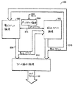
【0022】
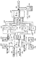
図3は、図1Aに示されるパケットストレージマネージャ106を示すブロック図である。パケットマネージャ106は、入力ポートエンジン104(図1A)からのセグメントバッファメモリ108への書込要求と、出力ポートエンジン110(図1A)からのセグメントバッファメモリ108からの読出要求とを、並行して扱う。
【0023】
パケットストレージマネージャ106は、読出アドレス論理300、読出アドレス論理302、ポートタイミング論理304およびアドレス選択論理312を含む。書込アドレス論理300は、入力ポート102(図1A)からのデータセグメントが記憶されるバッファセグメントメモリ108内の場所を提供する。読出アドレス論理300は、出力ポート112に対するデータパケットが記憶されているバッファセグメントメモリ108内の場所を提供する。
【0024】
アドレス選択論理312は、読出アドレス310および書込アドレス308をバッファセグメントメモリアドレス122に転送する。ポートタイミング論理304は、クロック306入力に応じてポートサイクル314を生成する。ポートタイミング論理304は、予め定められた数のクロック周期のポートサイクル時間208に対しポートサイクル314を生成し、予め定められたデータセグメントサイクル時間204ごとに各ポート102、112に対するポートサイクル314を生成する。データセグメントサイクル時間204は、入力ポート102(図1A)のいずれかで順次的にデータセグメントを受取るための時間に依存する。読出アドレス310および書込アドレス308は、ポートサイクル314に依存してポート102、112に対して選択される。ポートタイミング論理304によって、示されるように同じポートサイクル314が、書込アドレス論理300読出アドレス論理302に与えられるか、またはポートタイミング論理304によって、異なったポートサイクル314が、書込アドレス論理300および読出アドレス論理302に与えられてもよい。
【0025】
各ポートサイクル314の開始時に、読出アドレス論理302はポートサイクル314に依存して、ポートに対する読出アドレス論理302におけるポート待ち行列の先頭での先行して待ち行列に入れられた読出アドレス310を選択する。書込アドレス論理300は、読出アドレス論理302によって選択された読出アドレス310に依存して、ポートサイクル314に対する書込アドレスを選択する。
【0026】
アドレス選択論理312は、セグメントバッファメモリアドレス122を介して書込アドレス308および読出アドレス310をバッファセグメントメモリ108に転送する。セグメントバッファメモリ108に書込まれるべきデータパケットの書込アドレス308は、読出アドレス論理302内の待ち行列に入れられる。バッファセグメントメモリ108から読出されるべきデータパケットの読出アドレス302は、読出アドレス論理302内の待ち行列から外される。書込アドレス論理300および読出アドレス論理302は、図5、図6、図10および図11により詳細に示される。
【0027】
図4は、物理的に2つのバンク108Aおよび108Bに分割された、図1に示されたセグメントバッファメモリ108を示すブロック図である。セグメントバッファメモリ108の各バンクは関連のメモリアドレスであるアドレス A 400およびアドレス B 402を有する。二バンクアドレス選択論理404は、書込アドレス308に符号化されたセグメントバッファメモリ108のバンクに依存して、書込アドレス308をアドレス A 400またはアドレス B 402に転送する。二バンクアドレス選択論理404は、読出アドレス310に符号化されたバッファセグメントメモリ108のバンクに依存して、読出アドレス310をアドレス A 400またはアドレス B 402に転送する。たとえば、読出アドレス310および書込アドレス308の最上位のビット(「MSB」)を、セグメントバッファメモリ108Aおよび108Bのバンクを判断するために用いることができ、書込アドレス308および読出アドレス310は二バンクアドレス選択論理404によって転送される。書込アドレス論理300(図3)および読出アドレス論理304(図3)は、同じポートサイクル314(図2)の間に生成された読出アドレス308および書込アドレス310がセグメントバッファメモリ108A、Bの異なったバンクに対するものであることを確実にする。セグメントバッファメモリ108の一方のバンクに対する読出アクセスは、バッファセグメントメモリ108の他のバンクへの書込アクセスと並行して生じる。
【0028】
図5は、図4に示される2つのバンクのセグメントバッファメモリ108に対する図3に示される読出アドレス論理302を示すブロック図である。読出アドレス論理302は、ポート待ち行列選択論理512、ポート待ち行列510、および読出アドレス選択論理506を含む。ポート待ち行列510は、出力ポート112に与えられるべきデータパケットのセグメントバッファメモリにおけるアドレス場所を記憶する。出力ポート112ごとに別々のポート待ち行列510が与えられる。データセグメントがセグメントバッファメモリ108に書込まれるにつれて、データセグメントが書込まれた場所である書込アドレス308が1つ以上のポート待ち行列510に記憶される(または待ち行列に入れられる)。書込アドレス308が書込まれるべきポート待ち行列510は、ポート待ち行列選択論理512によって判断される。ポート待ち行列選択論理512は、転送ベクトル114に依存してポート待ち行列510を選択する。転送ベクトル114の生成は、図1Aを参照して説明した。
【0029】
ポート待ち行列510に記憶された書込アドレス308でのデータセグメントが、コピーが送られるべきすべての出力ポートによってセグメントバッファメモリ108から読出された後で、記憶された書込アドレス308はポート待ち行列510から外される。
【0030】
図6は、図3に示される2つのバンクのセグメントバッファメモリ108A、108Bに対する図2に示される書込アドレス論理300を示すブロック図である。2つのバンクのセグメントバッファメモリ108A、108Bに対する書込アドレス論理は、二バンク書込選択論理600、バンク Aに対する空きリスト606、バンク Bに対する空きリスト608、バンク Aに対する空きリストに対するカウント604、バンク Bに対する空きリストに対するカウント610、および書込アドレス選択論理602を含む。
【0031】
各空きリスト606、608は、データセグメントが書込まれるであろうセグメントバッファメモリのそれぞれのバンク108A、108Bにおける利用可能な場所を記憶する。バンク Aに対する空きリスト606は、セグメントバッファメモリ108Aのバンク Aにおける利用可能な場所を記憶し、バンク B 108Bに対する空きリストは、セグメントバッファメモリ108Bのバンク Bにおける利用可能な場所を記憶する。
【0032】
二バンク書込選択論理600は、ポートサイクル時間314の間に、読出アドレス310に依存して書込アドレス308が抽出されるべき空きリスト606、608を判断する。セグメントバッファメモリのバンク108A、108Bは、読出アドレス310のMSB、または読出アドレス310の他のビットに依存して選択され得る。たとえば、もし二バンク書込選択論理600が、読出アドレス310から、読出アドレス310はセグメントバッファメモリのバンク A108Aに対するものであると判断すると、書込アドレスはバンク Bに対する空きリスト608から抽出される。もし読出アドレス310が、バッファセグメントメモリのバンク B 108Bに対するものであれば、書込アドレスはバンク Aに対する空きリスト606から抽出される。こうして、データセグメントがセグメントバッファメモリ108の一方のバンクから読出されることができる一方、別のデータセグメントがセグメントバッファメモリ108の他方のバンクに書込まれる。
【0033】
もし二バンク書込選択論理600が、読出アドレスがバッファセグメントメモリのバンク A 108Aに対するものであると判断すると、これはENA B信号618によってバンク B空きリスト608をイネーブルし、それによりバンク B空きリスト608は書込アドレス選択論理602にバンク Bアドレス614を提供することができる。アドレスがバンク B空きリスト608から除去されると、二バンク書込選択論理600は獲得/更新カウントB信号616に更新カウント B信号を生成し、バンク Bに対する空きリストカウント610をデクリメントする。
【0034】
データセグメントが、書込アドレス308によって特定される場所でセグメントバッファメモリ108に書込まれる一方、書込アドレス308はそれぞれの空きリスト606、608から除去され、書込アドレス308は転送ベクトル114に依存して1つ以上のポート待ち行列306の最後に書込まれる。コピーカウント626が書込アドレス308に対してコピーカウント論理624に記憶される。コピーカウントは、マルチキャストパケット、すなわち1つ以上の出力ポート112に対して待ち行列に入れられるパケットを追跡するために用いられる。書込アドレス308は、読出アドレス308によって特定された場所が読出アドレス論理302(図3)によってすべて読出され、かつ書込アドレス308に関連のコピーカウントが0になった後で、それぞれの空きリスト606、608に返される。
【0035】
現在のポートサイクル314に対して読出されるべきデータセグメントがなく、書込まれるべきデータセグメントがあれば、二バンク書込選択論理600は空きリストカウント604、610に依存して書込アドレス308を抽出するべき空きリスト606、608を決定する。二バンク書込選択論理600は、獲得/更新カウント A信号622および獲得/更新カウント B信号616によって、バンク Aに対する空きリストカウント604およびバンク Bに対する空きリストカウント610から現在のカウントを獲得する。バンク Aに対する空きリストカウント632およびバンク Bに対する空きリストカウント630は、二バンク書込アドレス論理600に転送される。最大のカウントを備えた空きリストカウント604、610は、セグメントバッファメモリ108A、108Bの最も空いているバンクを示す。二バンク書込アドレス論理600はカウントを比較して、バンク Aカウント632またはバンク Bカウント630がより大きいかどうかに依存して、ENA A信号620またはENA B信号618を生成する。最大カウント604、610を備えた空きリスト606、608が選択される。書込アドレス308は選択された空きリスト606、608から選択される。こうして、データセグメントがセグメントバッファメモリ108に書込まれるにつれて、これらは均等に2つのバンクのセグメントバッファメモリ108A、108Bに分散される。
【0036】
図7は、図4に示される2つのバンクのセグメントバッファメモリ108に対する読出および書込アドレスに対するタイミングを示すタイミング図である。各データセグメントタイムスロット204において、スイッチ100に接続された64ポートごとにセグメントバッファメモリへの2つのアクセスが提供される。データセグメントタイムスロット204は、64ポートのいずれかでパケットセグメントを受取るための時間である。よって、データセグメント時間204は、スイッチ100に接続されるポートごとの、セグメントバッファメモリ108にパケットセグメントを記憶するために利用可能である最大の時間である。
【0037】
データセグメントタイムスロット204は、入力ポート112でデータが受取られる速度と、データ送信のために実現されるネットワークプロトコルとに依存する。たとえば、もし用いられるネットワークプロトコルが100メガヘルツイーサネット(R)であれば、1ビットは各ポートで10nsごとに受取られ、1バイトは80nsごとに受取られ、最小パケットサイズである64バイトは5120nsごとに受取られる。こうして、80nsのポートサイクル時間で、最小パケットサイズを、スイッチ100(図1A)に接続される各64 100MHzイーサネット(R)ポートで5120nsごとに記憶することができる。
【0038】
各ポートは、セグメントバッファメモリ108にアクセスするべきポートサイクル時間208を割当てられる。データセグメントは、ポートサイクル時間208ごとにセグメントバッファメモリ108における異なったアドレスに読出および書込を行なうことができる。ポートサイクル時間208は、データセグメントタイムスロット204およびスイッチ100に接続されるポートの数に依存する。
【0039】
時間700において、データセグメントタイムスロット208の開始で、フレームパルスはフレームパルス信号を発生させることにより生成される。フレームパルス信号は、ポートタイミング論理304(図3)を初期化するために用い得る。700で、ポート0に対するポートサイクル208が開始する。入力ポート0に対する書込アドレスは、バッファセグメントメモリ108Aに発信され得る一方、出力ポート0に対する読出アドレスはバッファセグメントメモリのBバンク108Bに送信され得る。
【0040】
時間702で、ポート1に対するポートサイクル208が開始する。入力ポート1に対する読出アドレスは、バッファセグメントメモリ108Aに発信され得る一方、出力ポート1に対する書込アドレスはバッファセグメントメモリのBバンク108Bに発信される。
【0041】
時間704で、データセグメントタイムスロット204の終了時に、フレームパルス信号を発生させることによりフレームパルスが生成される。ポートサイクルは、データセグメントタイムスロット204の間にスイッチに接続される64ポートごとに生成されている。
【0042】
図8は、図4に示される2つのバンクのセグメントバッファメモリ108A、108Bに対する読出および書込アドレスを選択するためのパケットストレージマネージャ106によって実行されるステップを示すフロー図である。図7に示されるようにポートサイクル208ごとに、読出および書込アドレスは同じポートに対するものであり、すなわち、入力ポート102および出力ポート112は同じポートである。しかしながら、入力ポート102および出力ポート112は示されるように同じポートである必要はなく、読出アドレスおよび書込アドレスは異なったポートに対するものであってもよい。図8は、図4から図7に関連して説明される。
【0043】
ステップ800において、二バンク書込選択論理600は、出力ポート112に対して保留された読出があるかどうかを判断する。もし保留された読出があれば、処理はステップ802に進む。もし保留された読出がなければ、処理はステップ822に続く。
【0044】
ステップ802において、二バンク書込選択論理600は、読出アドレスがどちらのセグメントバッファメモリのバンク108A、108Bに発信されるべきかをメモリアクセス論理312により判断する。もし読出アドレス310がバンク A 108Aに対するものであれば、処理はステップ812に進む。もし読出アドレス310がバンク B 108Bに対するものであれば、処理はステップ804に続く。
【0045】
ステップ804において、二バンク書込選択論理600がポートサイクル314に依存して保留された書込があるかどうかを判断する。もしポートに対して保留された書込があれば、処理はステップ810に進む。もしなければ、プロセスはステップ806に進む。
【0046】
ステップ810において、二バンク書込選択論理600は、バンク Aに対する空きリスト606から、セグメントバッファメモリのバンク A 108A内の利用可能な場所のアドレスを抽出する。バンク Aに対する空きリスト606からのバンク Aアドレス612は、書込アドレス選択論理602によって書込アドレス308として選択される。バンク Aに対する空きリストカウント604はデクリメントされる。書込アドレス308および読出アドレス310は、メモリアクセス論理312によってセグメントバッファメモリのそれぞれのバンク108A、108Bに転送される。プロセスはステップ808に進む。
【0047】
ステップ806において、読出アドレスがメモリアクセス論理312によってセグメントバッファメモリのバンク B 108Bに転送される。処理はステップ808に進む。
【0048】
ステップ808において、読出動作が完了した後で、コピーカウント論理624によって読出アドレスに対するコピーカウント626がデクリメントされる。読出アドレス310はバンク Bに対する空きリスト608に返され、コピーカウント626が0であればバンク Bに対する空きリストカウント610がインクリメントされる。処理はステップ820に進む。
【0049】
ステップ822において、書込選択論理600はポートに対して保留された書込があるかどうかを判断する。もしそのポートに対して書込が保留されていれば、処理はステップ824に続く。そうでなければ、処理はステップ820に続く。
【0050】
ステップ824において、書込選択論理600はセグメントバッファメモリのどちらのバンク108A、108Bが最も空いているかを、バンク Aに対する空きリストカウント604に記憶されているカウントおよびバンク Bに対する空きリストカウント610に記憶されているカウントから判断する。書込選択論理がセグメントバッファメモリのバンク A 108Aが最も空いていると判断すると、処理はステップ828に続く。二バンク書込選択論理600がセグメントバッファメモリのバンク B 108Bが最も空いていると判断すると、処理はステップ830に続く。
【0051】
ステップ828において、書込選択論理600は、バンク Aに対する空きリスト606からセグメントバッファメモリのバンク A 108Aにおける利用可能な場所のアドレスを除去する。バンク Aに対する空きリスト606からのバンク Aアドレス612は、書込アドレス選択論理602によって書込アドレス308として選択される。バンク Aアドレス612がバンク Aに対する空きリスト606から除去されると、バンク Aに対する空きリストカウント604がデクリメントされる。書込アドレス308は、メモリアクセス論理312(図3)によってバッファセグメントメモリのバンク A 108Aに転送される。
【0052】
ステップ830において、書込選択論理600は、バンク Bに対する空きリスト608から、セグメントバッファメモリのバンク B 108Bの利用可能な場所のアドレスを除去する。バンク Bに対する空きリスト608からのバンク Bアドレス614は、書込アドレス選択論理602によって書込アドレス308として選択される。バンク Bに対する空きリスト608からバンク Bアドレス614が除去されると、バンク Bに対する空きリストカウント610はデクリメントされる。書込アドレス308は、アドレス選択論理312(図3)によってバッファセグメントメモリのバンク B 108Bに転送される。
【0053】
ステップ812において、書込論理600は、ポートに対して保留された書込動作があるかどうかを判断する。もし保留された書込があれば、処理はステップ816に進む。なければ、処理はステップ814に進む。
【0054】
ステップ816において、書込選択論理600は、バンク Bに対する空きリスト608から、セグメントバッファメモリのバンクB 108Bの利用可能な場所のアドレスを除去する。バンク Bに対する空きリスト608からのバンク Bアドレス614は、書込アドレス選択論理602によって書込アドレス308として選択される。バンク Bに対する空きリスト608からバンク Bアドレス614が除去されると、バンク Bに対する空きリストカウント610がデクリメントされる。書込アドレス308および読出アドレス310は、メモリアクセス論理312(図3)によってバッファセグメントメモリのそれぞれのバンク108A、108Bに転送される。処理はステップ818に進む。
【0055】
ステップ814において、読出アドレス310は、アドレス選択論理312(図3)によってセグメントバッファメモリのバンク A 108Aに転送される。処理はステップ818に続く。
【0056】
ステップ818では、読出動作が終了すると、読出アドレスのコピーカウントはコピーカウント論理624によって減分される。読出アドレス310はバンク_Aに対する空きリスト606に返され、バンク_Aの空きリストカウント604はコピーカウントがゼロであるのなら増分される。処理はステップ820に続く。
【0057】
ステップ820では、ポートタイミング論理304(図2)は次のポートサイクル314に増分される。処理は次のポートサイクルに対してステップ800で続く。
【0058】
図9は図1Aに示されるセグメントバッファメモリを示すブロック図であり、セグメントバッファメモリは物理的に4個のバンク、すなわちセグメントバッファメモリ(バンク_A(偶数))(Ae)108Ae、セグメントバッファメモリ(バンク_A(奇数))(Ao)108Ao、セグメントバッファメモリ(バンクB(偶数))(Be)108Be、およびセグメントバッファメモリ(バンクB(奇数))(Bo)108Boに分けられる。メモリアドレスの2つのMSBに依存して、たとえばAまたはBのバンクを選択するMSBビットおよび奇数または偶数バンクを選択するMSB−1メモリアドレスに依存して、メモリは物理的に4個のバンクに分けられる。
【0059】
セグメントバッファメモリ108の各バンクは関連するメモリアドレス、すなわちアドレス_Ae 900、アドレス_Ao 902、アドレス_Be 904、およびアドレス_Bo 906を有する。メモリアクセス論理12は、書込アドレス308に符号化されるセグメントバッファメモリ108のバンクおよびポートサイクルに依存して、書込アドレス308をアドレス_Ae 900、アドレス_Ao 902、アドレス_Be 904またはアドレス_Bo 906に送る。メモリアドレス論理312は、読出アドレス310に符号化されるセグメントバッファメモリ108のバンクおよびポートサイクルに依存して、読出アドレス310をアドレス_Ae 900、アドレス_Ao 902、アドレス_Be 904またはアドレス_Bo 906に送る。
【0060】
データセグメント時間当り各ポートに与えられるメモリバンド幅は、各データセグメント時間において各ポートに対して2つのポートサイクル314、すなわち偶数ポートサイクルおよび奇数ポートサイクルを実施することにより、2倍に増加する。偶数バンク108Aeおよび108Beは偶数サイクルでアクセスされ、奇数バンク108Aoおよび108Boは奇数サイクルでアクセスされる。書込アドレス論理300(図2)および読出アドレス論理304(図2)は、各ポートサイクルで発行された読出アドレス308および書込アドレス310がバッファセグメントメモリ108Ae、108Ao、108Be、および108Boの異なるバンク用であることを確実にする。したがって、偶数サイクルの際、バンク_Ae 108Aeへの読出アクセスは、バンクBe 108Bへの書込アクセスと並行に起こる。
【0061】
データセグメント時間ごとに、各ポートに対して2つのポートサイクルを与え、かつ各ポートサイクルに並行な読出および書込アクセスを与えることにより、セグメントバッファメモリ108のバンド幅は、スイッチ100に接続される各ポートに対して4倍になる。したがって、各データセグメント時間において、各ポートに対して4回セグメントバッファメモリ108をアクセスすることができる。メモリアクセスは対で与えられ、1つの偶数バンクの読出動作がほかの偶数バンクへの書込動作と並行に行なわれる。
【0062】
図10は図9に示される四バンクセグメントバッファメモリ108に対する、図3に示される読出アドレス論理302を示すブロック図である。読出アクセス論理302(図3)は偶数/奇数ポート待ち行列選択論理1000、各出力ポート112に対するポート待ち行列510、および偶数/奇数読出アドレス選択論理1004を含む。四バンクセグメントバッファメモリ108に対して、ポートタイミング論理304(図3)は所定の数のクロック周期に偶数ポートサイクル106および奇数ポートサイクル108をそれぞれ生成し、各データセグメントタイムスロット204(図2)において偶数/奇数信号1010を生成する。偶数ポートサイクル1006および奇数ポートサイクル1008のタイミング図の例は図10と関連して説明される。
【0063】
ポート待ち行列510は既に図5と関連して記載されている。偶数/奇数ポート待ち行列選択論理1000は、奇数ポートサイクル1006および偶数ポートサイクル1008の状態ならびにポートタイミング論理304(図3)からの偶数/奇数信号1010に依存して、読出すべきポート待ち行列510を選択する。ポートに対して奇数ポートサイクル1006または偶数ポートサイクル1008のどちらかが活性状態の場合、ポートに対して読出すべき次のデータセグメントの場所504はポート待ち行列510から選択され、偶数/奇数読出アドレス選択論理1004に送られる。
【0064】
偶数/奇数読出アドレス場所選択論理1004は偶数ポートサイクル1006および奇数ポートサイクル1008の状態に依存して、ポート待ち行列510によって与えられるアドレス504を送る。場所504が奇数であり、かつ奇数ポートサイクル1008が活性状態にある場合、場所504は偶数/奇数読出アドレス選択論理1004に送られる。場所504が奇数でありかつ偶数ポートサイクル1006が活性状態にある場合、場所504は偶数/奇数読出アドレス選択論理1004に送られないが、場所504が偶数であるのなら場所504は送られる。したがって、データセグメント時間において、データセグメントがセグメントバッファメモリ108の奇数および偶数バンクに記憶されているのなら、ポートはセグメントバッファメモリ108からデータセグメントの2つの場所を読出し得る。
【0065】
図11は、図9に示される四バンクセグメントバッファメモリ108のための、図2に示される書込アドレス論理を示すブロック図である。四バンク書込選択論理1100はセグメントバッファメモリ108Ao、108Ae、108Boおよび108Beの4つのバンクの1つに対する書込アドレス308を選択する。バッファセグメントメモリ108Ao、108Ae、108Boおよび108Beの各バンクは、関連する空きリスト1112、1114、1116および1118ならびに空きリストカウント1102、1104、1106および1108を有する。
【0066】
四バンク書込選択論理1100は、読出アドレス310および偶数/奇数信号910に依存して、書込アドレスを抽出するべき空きリスト1112、1114、1116および1118を定める。四バンク書込選択論理1100は、偶数/奇数信号910からメモリアクセスが偶数サイクル用でありかつ読出アドレス310はバッファセグメントメモリ108AeのAeバンク用であると定めたなら、書込アドレスはBeバンクの空きリスト1106から抽出される。四バンク書込選択論理1100は、偶数/奇数信号910からメモリアクセスは偶数サイクル用であり、かつ読出アドレス310はバッファセグメントメモリ308BeのBeバンク用であると定めたなら、書込アドレスはAeバンクの空きリスト1112から抽出される。
【0067】
四バンク書込選択論理1100は読出アドレスがバッファセグメントメモリ108AeのAeバンク用であると定めるのなら、ENA_3信号1134を通してBeバンクの空きリスト1116を能動化し、それによりBeバンクの空きリスト1116は四バンク書込アドレス選択論理1120に対してBeバンクアドレス1126を与えることができる。Beバンク用の空きリストからアドレスが取除かれると、四バンク書込選択論理1100は獲得/更新カウントBe信号1140に更新カウントBe信号を生成して、バンク_Beの空きリストカウント1140を減分することにより、Beバンクの空きリスト1116を更新する。
【0068】
有効な読出アドレスがない場合、四バンク書込選択論理1100は空きリストカウント1102、1104、1106、および1108に依存して、書込アドレス308を抽出するべき空きリスト1112、1114、1116および1118を定める。最も大きい値を有する空きリストカウント1102、1104、1106および1108は、最大の利用可能な場所を有するセグメントバッファメモリ108Ae、108Ao、108Be、108Boのバンクを示す。空きリストカウント1102、1104、1106および1108における最大の利用可能な場所に関連する空きリスト1112、1114、1116および1118は選択されて、書込まれるべきセグメントバッファメモリ108の次の場所を与える。こうして、データが書込まれる際に、バッファセグメントメモリ108Ae、108Ao、108Boおよび108Beのバンク間で均等に配分される。
【0069】
たとえば、偶数のポートサイクルに対して読出アドレス310がなければ、四バンク書込選択論理1100は獲得/更新カウントAe信号1144および獲得/更新カウントBe1140信号を通して、Aeバンク用の空きリストカウント1102およびBeバンク用の空きリストカウント1106から現行のカウントを得る。バンク_Ae用の空きリストカウント1102およびバンク_Be用の空きリストカウント1106は四バンク書込アドレス論理1100に送られる。四バンク書込アドレス論理1000はカウント値を比較し、バンク_Aeのカウント1102およびバンク_Beのカウント1106のどちらが大きいかに依存して、ENA_1信号1130またはENA_3信号1134を生成する。
【0070】
空きリスト書込アドレス1122、1124、1126および1128のうち1つが選択されると、書込アドレス308は四バンク書込アドレス選択論理1120によってセグメントバッファメモリ108に送られる。コピーカウント626は書込アドレス308用のコピーカウント論理624に記憶される。コピーカウント626はマルチキャストパケットを管理するために用いられる、すなわちパケットが2つ以上の出力ポート112に対して待ち行列に入れられる。
【0071】
図12は図9に示される四バンクセグメントバッファメモリ108の読出および書込アドレスのタイミングを示すタイミング図である。各データセグメントタイムスロット204において、スイッチ100に接続される64個のポートの各々に対して、セグメントバッファメモリへのアクセスが4回与えられる。データセグメントタイムスロット204は64個のポートのうちのいずれかのポートでデータセグメントを受取る時間である。したがって、データセグメント時間204は、スイッチ100に接続される各ポートに対して、セグメントバッファメモリ108にデータセグメントを記憶するのに利用できる最長の時間である。
【0072】
各ポートは、セグメントバッファメモリ108をアクセスするべきポートサイクル時間208が割当てられている。データセグメントはポートサイクル時間208の間に、ポート用のデータセグメントメモリのバンクに対して読出または書込される。ポートサイクル時間208はデータセグメントタイムスロット204およびスイッチ100に接続されるポートの数に依存する。セグメントバッファメモリ108(図1A)のアクセス時間はポートサイクル時間208に依存する。
【0073】
1204において、各データセグメントタイムスロット204が開始されるとき、フレームパルス信号をパルス化することによりフレームパルスが生成される。フレームパルス信号はポートタイミング論理304(図3)を初期化するために用いることができる。1206において、ポート0用の偶数サイクルが開始される。ポート0用の書込アドレスはバッファセグメントメモリ108AeのAeバンクに送られ、ポート0の読出アドレスはバッファセグメントメモリ108BeのBeバンクに送られる。時間1214において、ポート32の奇数サイクルが開始され、ポート32の書込アドレスはバッファセグメントメモリ108BoのAoバンクに送られ、ポート32の読出アドレスはバッファセグメントメモリ108BoのBoバンクに送られる。ポート32の奇数サイクルの開始1214は、ポート0の偶数サイクルの開始1206後、ポートサイクル時間208の半分の時間から始まる。この偶数サイクルの開始および奇数サイクルの開始間の遅れにより、奇数サイクルおよび偶数サイクルにおいてバッファセグメントメモリ108に共通論理を使用することができる。共通論理が用いられないのなら、奇数サイクルの開始および偶数サイクルの開始は同じ時間にスケジュールされ得る。
【0074】
1218において、ポート0の奇数サイクルの開始は、データセグメントタイムスロット204の半分の時間に、ポート0の偶数サイクルの開始からポートタイムスロット208の半分の時間を加えた時間としてスケジュールされる。この時間は図12における遅延時間1220である。たとえば、データセグメントタイムスロット204が5120ns(64バイト、バイト当り8ビット、バイト当り10ns)であり、ポート0の偶数ポートサイクルの開始1206が0で始まるのなら、ポート0の奇数ポートサイクルの開始は、ポート0の偶数ポートサイクルの開始1206から2200ns(5120/2+40)にスケジュールされる。
【0075】
データセグメントタイムスロット204において、スイッチ100はデータセグメントサイズの倍数でないバイトカウントのデータパケットを受取ることができる。これらのデータパケットは最小のデータパケットとして受取られる時間とほぼ同じ時間をとる。たとえば、データセグメントタイムスロット204内で入力ポート0で受取られた65バイトのデータパケットを記憶するのに、ポート0の偶数サイクルの間最初の64バイトがセグメントバッファメモリ108に書込まれ、最後のバイトはポート0の奇数サイクルの際にセグメントバッファメモリ108に書込まれる。
【0076】
スイッチ100は1データセグメントより大きいデータパケットを受取ることができる。同じデータパケットのデータを受けながら、四バンク書込選択論理1100はパケット信号1138を通して、同じパケットの順次データセグメント用の書込アドレス208が交互の偶数および奇数空きリストから選択されることを確実にする。たとえば、最初のセグメントが偶数バンク_Bの空きリスト1116から選択された書込アドレス308に書込まれるのなら、次の順次セグメントはバンク_A 108Aoまたはバンク_B 108Boからの読出があるかどうかに依存して、奇数バンク_Bの空きリスト1108または奇数バンク_Aの空きリスト1114から選択された書込アドレス308に書込まれる。
【0077】
図13は図9に示される四バンクセグメントバッファメモリの偶数バンク用の読出および書込アドレスを選択するステップを示すフロー図である。
【0078】
図13は図9に示される四バンクセグメントバッファメモリの偶数バンク用の読出および書込アドレスを選択するステップを示すフロー図である。
セグメントバッファメモリ108Aeおよび108Beの偶数バンクは偶数ポートタイムスロットで選択される。同じステップは奇数ポートタイムスロットにおいてセグメントバッファメモリ108Aoおよび108Aeの奇数バンク用に読出および書込アドレスを選択するために行なわれる。図12に示されるように、偶数ポートタイムスロットの際の読出および書込動作は同じポートに対して発行される、すなわち入力ポート102および出力ポート112は同じポートである。入力ポート102および出力ポート112は示されているように同じポートである必要はなく、読出動作および書込動作は並行に異なるポートに対して発行され得る。図13は図9−図12に関連して記載される。
【0079】
ステップ1300において、4四バンク書込選択論理1100は出力ポート112用の保留読出を示す、読出選択論理1004からの有効な読出アドレス310があるかどうかを定める。保留の読出があるのなら、処理はステップ1304で続けられる。なければ、処理はステップ1328に続く。
【0080】
ステップ1304において、四バンク読出選択論理1004はメモリアクセス論理312によって読出アドレスがセグメントバッファメモリ108Aeおよび108Beのどの偶数バンクに発行されるのかを定める。読出アドレス310が偶数バンク_A 108Ae用であるのなら、処理はステップ108に進む。読出アドレス310が偶数バンク_B 108Be用であるのなら、処理はステップ1306に進む。
【0081】
ステップ1308において、四バンク書込選択論理1100は入力ポート102に対して保留の書込があるかどうかを定める。入力ポートに対して保留書込があるのなら、処理はステップ1320に進む。なければ、処理はステップ1318に進む。
【0082】
ステップ1320において、四バンク書込選択論理1100はENA_3信号1134を通して偶数バンク_Bの空きリスト1116からセグメントバッファメモリ108Beの偶数バンク_Bに対する利用可能なアドレスを抽出する。バンク_Bの偶数バンク_B空きリスト1116からの偶数バンク_Bアドレス1126は四バンク書込アドレス選択論理1120によって書込アドレス308として選択される。偶数バンク_B空きリストカウント1106は獲得/更新カウントBe信号1140によって減分される。書込アドレス308および読出アドレス310は四バンク読出/書込アドレス選択論理908(図9)を通してセグメントバッファメモリ108Aeおよび108Beのそれぞれの偶数バンクに送られる。処理はステップ1324に進む。
【0083】
ステップ1318において、読出アドレス310は四バンク読出/書込アドレス選択論理908によって、セグメントバッファメモリ108Aeの偶数バンク_Aに送られる。処理はステップ1324に進む。
【0084】
ステップ1324において、読出動作が終了すると、読出アドレス310は偶数バンク_Aの空きリスト1112に返され、コピーカウント626(図6)がゼロであれば偶数バンク_Aの空きリストカウント1102は増分される。処理はステップ1326に進む。
【0085】
ステップ1328において、四バンク書込選択論理1100はポートに対して書込の保留があるかどうか定める。ポートに対して書込保留があるのなら、処理はステップ1330に進む。なければ、処理はステップ1326に進む。
【0086】
ステップ1330において、四バンク書込選択論理1100は、偶数バンク_Aの空きリストカウント1102に記憶されるカウントおよび偶数バンク_Bの空きリストカウント1106に記憶されるカウントから、バッファセグメントメモリ108Aeおよび108Beのどの偶数バンクが最も空いているかを定める。書込選択論理はセグメントバッファメモリ108Aeの偶数バンク_Aが最も空いていることを定めると、処理はステップ1334に進む。四バンク書込選択論理1100はセグメントメモリ108Beの偶数バンク_Bが最も空いていると定めると、処理はステップ1336に続く。
【0087】
ステップ1334において、四バンク書込選択論理1100は偶数バンク_Aの空きリスト1112から、セグメントバッファメモリ108Aeの偶数バンク_Aの利用可能な場所のアドレスを取除く。偶数バンク_Aの空きリスト1112からのバンク_Aアドレス1122が、四バンク書込アドレス選択論理1120によって書込アドレス308として選択される。偶数バンク_Aアドレス1122が偶数バンク_Aの空きリスト1112から取除かれる際、偶数バック_Aの空きリストカウント1102は減分される。書込アドレス308は四バンク読出/書込アドレス選択論理908(図9)によって、セグメントバッファセグメントメモリ108Aeの偶数バンク_Aに送られる。
【0088】
ステップ1336において、四バンク書込選択論理1100は偶数バンク_Bの空きリスト1116から、セグメントバッファメモリ108Beの偶数バンク_Bから利用可能なアドレスを取除く。偶数バンク_Bの空きリスト1116からの偶数バンク_Bアドレス1126は、四バンク書込アドレス選択論理1120によって書込アドレス308として選択される。偶数バンク_Bアドレス1126が偶数バンク_Bの空きリスト1106から取除かれる際、偶数バンク_Bの空きリストカウント1106が減分される。書込アドレス308は四バンク読出/書込アドレス選択論理908(図9)によって、バッファセグメントメモリ108Beの偶数バンク_Bに送られる。
【0089】
ステップ1306において、四バンク書込選択論理1100はポートに対して書込動作が保留であるかどうか定める。書込保留があるのなら、処理はステップ1316に進む。なければ、処理はステップ1312に続く。
【0090】
ステップ1316において、四バンク書込選択論理1100は偶数バンク_Aの空きリスト1112から、セグメントバッファメモリ108Aeの偶数バンク_Aにおける利用可能なアドレスを取除く。偶数バンク_Bの空きリスト1116からの偶数バンクAアドレス1122は、四バンク書込アドレス選択論理1120によって、書込アドレス308として選択される。偶数バンク_Aアドレス1122が偶数バンク_Aの空きリスト1112から取除かれる際、偶数バンク_Aの空きリストカウント1102は減分される。書込アドレス308および読出アドレス310は、四バンク読出/書込アドレス選択論理908(図9)によって、セグメントバッファメモリ108Aeおよび108Beのそれぞれのバンクに送られる。処理はステップ1322に進む。
【0091】
ステップ1312において、読出アドレス310は、四バンク読出/書込アドレス選択論理908(図9)によって、セグメントバッファメモリ108Beの偶数バンク_Aに送られる。処理はステップ1322に進む。
【0092】
ステップ1322において、読出動作が終了すると、読出アドレス310は偶数バンク_Aの空きリスト1112に返され、コピーカウント626(図6)がゼロであれば偶数バンク_Aの空きリストカウント1102が増分される。処理はステップ1326に進む。
【0093】
ステップ1326において、次の偶数ポートタイムスロットの処理が始まる。次の偶数ポートサイクルはポートタイミング論理304(図3)によって定められる。
【0094】
本発明は、図4−図6に関連して記載されている2つのバンクまたは図9−図13に関連して記載される4つのバンクに分けられる、バッファセグメントメモリ108(図1A)に限定されない。バッファセグメントメモリ108は2N(ここでN=1、2、3、4…)個の任意な数のバンクに分けられ得る。
【0095】
本発明は特定的に示されかつ好ましい実施例を参照して記載されているが、前掲の特許請求の範囲によって含まれる発明の範囲から逸脱することなく、形および詳細においてさまざまな変形が可能であることは理解されるであろう。
【図面の簡単な説明】
【図1A】 非ブロッキング共通メモリスイッチのブロック図である。
【図1B】 入力ポートで受取られるべき先行技術のイーサネット(R)データパケットのブロック図である。
【図2】 スイッチ内の共通メモリによる入力ポートから出力ポートへの転送を示すタイミング図である。
【図3】 図1Aに示される、パケットストレージマネージャ106を示すブロック図である。
【図4】 物理的に2つのバンクに分割された、図1Aに示されるセグメントバッファメモリ108を示すブロック図である。
【図5】 図4に示される二バンクセグメントバッファメモリに対する図3に示される読出アドレス論理302を示すブロック図である。
【図6】 図4に示される二バンクセグメントバッファメモリに対する図3に示される書込アドレス論理を示すブロック図である。
【図7】 図4に示される二バンクセグメントバッファメモリに対する読出および書込アドレスのタイミングを示すタイミング図である。
【図8】 図4に示される二バンクセグメントバッファメモリに対する読出および書込アドレスを選択するためのステップを示すフロー図である。
【図9】 物理的に4つのバンクに分割された、図1Aに示されるセグメントバッファメモリを示すブロック図である。
【図10】 図9に示される四バンクセグメントバッファメモリに対する図3に示される読出アドレス論理を示すブロック図である。
【図11】 図9に示される四バンクセグメントバッファメモリに対する図3に示される書込アドレス論理を示すブロック図である。
【図12】 図9に示される四バンクセグメントバッファメモリに対する読出および書込アドレスのタイミングを示すタイミング図である。
【図13】 図9に示される四バンクセグメントバッファメモリの偶数のバッファに対する読出および書込アドレスを選択するためのステップを示すフロー図である。[0001]
BACKGROUND OF THE INVENTION
The network switch receives data packets from several input ports connected to the switch and provides the data packets to several output ports connected to the switch. The switch determines an output port to which the data packet is to be given, depending on the destination address included in the data packet. Data packets received from the input port are stored in memory in the switch before being applied to the output port.
[0002]
The memory in the switch may be a common memory that is stored before all data packets received from all input ports are presented to the output port. A non-blocking switch allows all data received at all input ports to be provided to the output port. Non-blocking switches typically include a common memory to make the maximum amount of memory available per port.
[0003]
The speed of the common memory switch depends on the memory bandwidth. Memory bandwidth depends on memory access time and memory width, which is the number of bytes accessed per memory access time. For example, if the common memory is 64 bytes wide and has an access time of 80 nanoseconds (ns), it takes 80 ns to write or read 64 bytes. When the input port connected to the switch receives data at 100 megabits (M) bps (bits per second), 1 bit is received every 10 ns, 8 bit bytes are received every 80 ns, and 64 bytes are 5120 ns. Received every time. After 64 bytes of data are received, a write memory cycle is performed to write 64 bytes with a single access to the 64 byte wide memory. The input port uses the memory bandwidth of 80 ns every 5120 ns to write the received data to the memory. Thus, a 64 byte wide memory with 80 ns access time can support 64 (5120 ns / 80 ns) 100 Mbps ports. If 64 ports are connected to the switch, each port cycle is 80 ns. The 80ns port cycle provides each port with one memory access per port cycle.
[0004]
Increasing the memory bandwidth available in each port cycle requires one or more of the following: reduced memory access time, memory width (ie read / write per memory cycle) Increase the number of bits) or decrease the number of ports. The increase in memory width is limited by the minimum data packet size. The reduction in memory access time is limited by the minimum memory access time for the memory.
[0005]
The memory bandwidth can also be increased, for example, by interleaving the memory bank for writing the first data packet to the first memory bank and writing the second data packet to the second data bank. However, interleaving the data in the switch can lead to blocking, for example if both port A and port B are requesting access to the first memory bank at the same time. Blocking data transfer between the input and output ports can lead to dropped packets. Thus, it cannot be used to increase the memory bandwidth in a non-blocking switch.
[0006]
SUMMARY OF THE INVENTION
The packet storage manager at the switch increases the memory bandwidth of the memory shared by the input and output ports connected to the switch. The packet storage manager uses a single port cycle to write to one of the input ports and one of the output ports where the prior art system required sequential read and write cycles. Both read operations are performed. Write and read operations are performed in parallel on different memories in the memory in a single memory access cycle. The memory is physically divided into several banks. The number of banks is preferably two or four. Read and write operations are performed on different banks.
[0007]
The packet storage manager has a read address logic for selecting a read address in the memory for the read operation depending on the port cycle, and a write for the write operation depending on the read address selected by the read address logic. Write address logic for selecting an address. The write address is selected depending on the read address so that the read and write operations can be performed in parallel with a single memory access. The packet storage manager relies on a port queue for each output port and a free list of addresses not stored in the port queue. From the incoming packet, the manager reads the network destination and determines the appropriate output port where the packet should be stored. The manager writes the packet segment to memory by removing the memory segment address from the free list, stores the segment address at the end of each port queue to which the packet should be directed, and in the location in memory specified by the segment address Write a packet segment. At the same time, the address at the beginning of each port queue identifies the packet segment to be read by the manager.
[0008]
Read address logic within the packet storage manager includes a port queue for each output port. The port queue stores memory locations for data written to memory by each input port. Port queue selection logic, depending on the port cycle, selects the port queue from which memory addresses are to be removed. The read selection logic selects the memory location to be read depending on the memory address removed from the port queue.
[0009]
The memory is physically divided into several banks. The number of banks is preferably two or four. The write address logic within the packet storage manager includes a bank free list for each bank. Each bank free list stores the addresses of available locations within a bank of memory. Write selection logic within the write address logic selects one of the bank empty lists from which the write address is to be removed. Write selection logic selects the bank free list so that sequential segments of data packets are written to alternating odd and even banks of memory.
[0010]
The write address logic also includes a bank free list counter for each bank. The bank free list counter stores a count of available locations in the bank. Write selection logic may select a bank empty list depending on the count in the bank empty list counter. Parallel read and write operations may be for the same port or for different ports.
[0011]
The above objects as well as other objects and features and advantages of the present invention will become apparent from the more specific description of the preferred embodiment of the invention as illustrated in the accompanying drawings, in which like elements Are given the same reference numerals throughout the different figures. The drawings are not necessarily on the same scale as the real thing, and emphasis is placed on illustrating the principles of the invention.
[0012]
DESCRIPTION OF THE INVENTION
FIG. 1A is a block diagram of the
[0013]
The
[0014]
The
[0015]
The
[0016]
As data packets are received sequentially at one of the
[0017]
FIG. 1B is a block diagram illustrating a prior art
[0018]
FIG. 2 is a timing diagram illustrating switching of data received at
[0019]
Between
[0020]
The data
[0021]
Thus, when a data segment is received at
[0022]
FIG. 3 is a block diagram illustrating the
[0023]
The
[0024]
[0025]
At the start of each
[0026]
The
[0027]
FIG. 4 is a block diagram illustrating the
[0028]
FIG. 5 is a block diagram illustrating the read
[0029]
After the data segment at
[0030]
FIG. 6 is a block diagram illustrating the
[0031]
Each
[0032]
The two-bank
[0033]
If the two-bank
[0034]
While the data segment is written to the
[0035]
If there is no data segment to be read for the
[0036]
FIG. 7 is a timing diagram showing timings for read and write addresses for the
[0037]
The data
[0038]
Each port is assigned a
[0039]
At
[0040]
At
[0041]
At
[0042]
FIG. 8 is a flow diagram illustrating the steps performed by the
[0043]
In step 800, the two bank write
[0044]
In
[0045]
In
[0046]
In
[0047]
In step 806, the read address is stored in the bank of segment buffer memory by
[0048]
In
[0049]
In
[0050]
In
[0051]
In
[0052]
In
[0053]
In
[0054]
In
[0055]
In step 814, read
[0056]
In step 818, when the read operation is complete, the copy count of the read address is decremented by the
[0057]
In
[0058]
FIG. 9 is a block diagram showing the segment buffer memory shown in FIG. 1A. The segment buffer memory is physically divided into four banks, that is, segment buffer memory (bank_A (even number)) (Ae) 108Ae, segment buffer memory ( Bank_A (odd number)) (Ao) 108Ao, segment buffer memory (bank B (even number)) (Be) 108Be, and segment buffer memory (bank B (odd number)) (Bo) 108Bo. Depending on the two MSBs of the memory address, for example, depending on the MSB bit that selects the A or B bank and the MSB-1 memory address that selects the odd or even bank, the memory is physically divided into four banks. Divided.
[0059]
Each bank of
[0060]
The memory bandwidth provided to each port per data segment time is doubled by performing two
[0061]
For each data segment time, the bandwidth of
[0062]
10 is a block diagram showing the
[0063]
[0064]
The even / odd read address
[0065]
11 is a block diagram illustrating the write address logic shown in FIG. 2 for the four bank
[0066]
Four-bank write
[0067]
If the four bank write
[0068]
If there is no valid read address, the four bank write
[0069]
For example, if there is no
[0070]
When one of the free list write addresses 1122, 1124, 1126 and 1128 is selected, the
[0071]
FIG. 12 is a timing chart showing the timing of the read and write addresses of the four bank
[0072]
Each port is assigned a
[0073]
At 1204, when each data
[0074]
At 1218, the start of the odd cycle of port 0 is scheduled as half the time of the data
[0075]
In the data
[0076]
The
[0077]
FIG. 13 is a flow chart showing steps for selecting read and write addresses for even banks of the four bank segment buffer memory shown in FIG.
[0078]
FIG. 13 is a flow chart showing steps for selecting read and write addresses for even banks of the four bank segment buffer memory shown in FIG.
Even banks of segment buffer memories 108Ae and 108Be are selected in even port time slots. The same steps are performed to select read and write addresses for the odd banks of segment buffer memories 108Ao and 108Ae in odd port time slots. As shown in FIG. 12, read and write operations during even port time slots are issued to the same port, ie,
[0079]
In
[0080]
In step 1304, four bank read
[0081]
In
[0082]
In
[0083]
In
[0084]
When the read operation is completed in step 1324, the
[0085]
In
[0086]
In
[0087]
In
[0088]
In
[0089]
In step 1306, the four bank write
[0090]
In
[0091]
In step 1312, read
[0092]
When the read operation is completed in
[0093]
In
[0094]
The present invention is limited to the buffer segment memory 108 (FIG. 1A) that is divided into two banks as described in connection with FIGS. 4-6 or four banks as described in connection with FIGS. 9-13. Not.
[0095]
Although the invention has been particularly shown and described with reference to preferred embodiments, various changes in form and detail are possible without departing from the scope of the invention as encompassed by the appended claims. It will be understood that there is.
[Brief description of the drawings]
FIG. 1A is a block diagram of a non-blocking common memory switch.
FIG. 1B is a block diagram of a prior art Ethernet data packet to be received at an input port.
FIG. 2 is a timing diagram showing a transfer from an input port to an output port by a common memory in the switch.
FIG. 3 is a block diagram illustrating the
FIG. 4 is a block diagram illustrating the
5 is a block diagram illustrating the read
6 is a block diagram illustrating the write address logic shown in FIG. 3 for the two bank segment buffer memory shown in FIG.
FIG. 7 is a timing diagram showing read and write address timings for the two-bank segment buffer memory shown in FIG. 4;
FIG. 8 is a flow diagram showing steps for selecting read and write addresses for the two bank segment buffer memory shown in FIG. 4;
FIG. 9 is a block diagram illustrating the segment buffer memory shown in FIG. 1A physically divided into four banks.
10 is a block diagram illustrating the read address logic shown in FIG. 3 for the four bank segment buffer memory shown in FIG. 9;
11 is a block diagram illustrating the write address logic shown in FIG. 3 for the four bank segment buffer memory shown in FIG.
FIG. 12 is a timing diagram showing read and write address timings for the four bank segment buffer memory shown in FIG. 9;
FIG. 13 is a flow diagram showing steps for selecting read and write addresses for an even number of buffers of the four bank segment buffer memory shown in FIG. 9;
Claims (30)
複数の入力ポートと、
複数の出力ポートと、
複数の入力ポートと複数の出力ポートとによって共有され、複数の入力ポートのいずれかから受取った入力データストリームを記憶し、複数の出力ポートのいずれかに出力データストリームを与えるメモリと、
複数の出力ポートの1つに対するメモリ読出動作をスケジュールし、並行して複数の入力ポートの1つに対するメモリ書込動作をスケジュールするパケットストレージマネージャとを含み、メモリ読出動作およびメモリ書込動作は単一のポートサイクルでメモリの異なった部分に対してスケジュールされ、
パケットストレージマネージャは、
ポートサイクルに依存して、メモリ読出動作のためのメモリにおける第1の場所に対する読出アドレスを選択する読出アドレス論理を含み、読出アドレス論理は、
複数の出力ポートの各々に対するポート待ち行列を含み、ポート待ち行列は入来パケット内のネットワークデスティネーションに依存して、パケットストレージマネージャによってメモリに書込まれたデータの場所のメモリアドレスを記憶し、読出アドレス論理はさらに、
ポートサイクルに依存して、メモリ読出アドレスを取除くべきポート待ち行列を選択するポート待ち行列選択論理を含み、読出すべきメモリ部分は、選択されたポート待ち行列の先頭から取除かれたメモリ読出アドレスに依存し、パケットストレージマネージャはさらに、
読出アドレス論理によって選択された読出アドレスに依存して、メモリ書込動作のためのメモリにおける第2の場所に対する書込アドレスを選択する書込アドレス論理を含む、スイッチ。A switch,
Multiple input ports,
Multiple output ports,
A memory shared by a plurality of input ports and a plurality of output ports, storing an input data stream received from any of the plurality of input ports, and providing an output data stream to any of the plurality of output ports;
A packet storage manager that schedules a memory read operation to one of the plurality of output ports and concurrently schedules a memory write operation to one of the plurality of input ports. Scheduled for different parts of the memory in one port cycle,
Packet storage manager
Depending on the port cycle, includes a read address logic that selects a read address for a first location in the memory for a memory read operation,
A port queue for each of the plurality of output ports, the port queue depending on the network destination in the incoming packet and storing the memory address of the location of the data written to memory by the packet storage manager; Read address logic further
Depending on the port cycle, includes port queue selection logic to select the port queue to remove the memory read address, the memory portion to be read is the memory read removed from the head of the selected port queue Depending on the address, the packet storage manager
A switch comprising write address logic that selects a write address for a second location in the memory for a memory write operation, depending on the read address selected by the read address logic.
アドレスの空きリストと、
空きリストから書込アドレスを取除くことにより、メモリにおける書込アドレスを与える書込選択論理とを含み、
読出アドレス論理は、書込アドレスをパケットセグメントが方向付けられる各ポート待ち行列の最後に記憶し、
パケットストレージマネージャは、書込アドレスによって指定されるメモリの別の部分にパケットセグメントを書込む、請求項1に記載のスイッチ。The write address logic is
A free list of addresses,
Write selection logic to provide a write address in memory by removing the write address from the free list;
Read address logic stores the write address at the end of each port queue to which a packet segment is directed;
The switch of claim 1, wherein the packet storage manager writes the packet segment to another portion of memory specified by the write address.
複数のバンクの各々に対する空きリストカウンタをさらに含み、空きリストカウンタはバンクにおける利用可能な場所のカウントを記憶し、書込選択論理はこのカウントに依存して空きリストの1つを選択する、請求項6に記載のスイッチ。The write address logic further includes a free list counter for each of the plurality of banks, the free list counter stores a count of available locations in the bank, and the write selection logic depends on this count to determine one of the free lists. The switch according to claim 6, wherein
複数の入力ポートと、
複数の出力ポートと、
複数の入力ポートと複数の出力ポートとによって共有され、複数の入力ポートのいずれかから受取った入力データストリームを記憶し、複数の出力ポートのいずれかに出力データストリームを与えるメモリと、
複数の出力ポートの1つに対するメモリ読出動作をスケジュールし、並行して複数の入力ポートの1つに対するメモリ書込動作をスケジュールするための手段とを含み、メモリ読出動作およびメモリ書込動作は単一のポートサイクルでメモリの異なった部分に対してスケジュールされ、
スケジュールするための手段は、
ポートサイクルに依存して、メモリ読出動作のためのメモリにおける読出アドレスを選択するための手段を含み、読出アドレスを選択するための手段は、
複数の出力ポートの各々に対するポート待ち行列を含み、ポート待ち行列は入来パケット内のネットワークデスティネーションに依存して、スケジュールするための手段によってメモリに書込まれたデータの場所のメモリアドレスを記憶し、読出アドレスを選択するための手段はさらに、
ポートサイクルに依存して、読出アドレスを取除くべきポート待ち行列を選択するための手段を含み、読出すべきメモリ部分は、選択されたポート待ち行列の先頭から取除かれた読出アドレスに依存し、スケジュールするための手段はさらに、
読出アドレスを選択するための手段によって選択された読出アドレスに依存して、メモリ書込動作のためのメモリにおける書込アドレスを選択するための手段とを含む、スイッチ。A switch,
Multiple input ports,
Multiple output ports,
A memory shared by a plurality of input ports and a plurality of output ports, storing an input data stream received from any of the plurality of input ports, and providing an output data stream to any of the plurality of output ports;
Means for scheduling a memory read operation for one of the plurality of output ports and scheduling a memory write operation for one of the plurality of input ports in parallel. Scheduled for different parts of the memory in one port cycle,
The means for scheduling is
Depending on the port cycle, including means for selecting a read address in the memory for a memory read operation, the means for selecting the read address comprises:
A port queue for each of the plurality of output ports, the port queue storing the memory address of the location of the data written to the memory by means for scheduling, depending on the network destination in the incoming packet The means for selecting the read address is further
Depending on the port cycle, including means for selecting a port queue to remove the read address, the memory portion to be read depends on the read address removed from the head of the selected port queue. The means for scheduling are further
Means for selecting a write address in the memory for a memory write operation depending on the read address selected by the means for selecting a read address.
アドレスの空きリストと、
空きリストから書込アドレスを取除くための手段とを含み、
読出アドレスを選択するための手段は、セグメントが方向付けられている各ポート待ち行列の最後に書込アドレスを記憶し、
取除くための手段は、スケジュールするための手段にパケットを書込むための書込アドレスを与え、スケジュールするための手段は、書込アドレスによって指定されたメモリの
別の部分にセグメントを書込む、請求項11に記載のスイッチ。Means for selecting a write address are:
A free list of addresses,
Means for removing the write address from the free list;
Means for selecting a read address stores a write address at the end of each port queue to which a segment is directed;
The means for removing provides a write address for writing the packet to the means for scheduling, and the means for scheduling writes the segment to another portion of the memory specified by the write address; The switch according to claim 11.
複数のバンクの各々に対する空きリストカウンタをさらに含み、空きリストカウンタはバンクにおける利用可能な場所のカウントを記憶し、書込アドレスを選択するための手段は空きリストカウンタにおけるカウントに依存して空きリストの1つを選択する、請求項17に記載のスイッチ。Means for selecting a read address are:
A free list counter for each of the plurality of banks, the free list counter storing a count of available locations in the bank, and means for selecting a write address depends on the count in the free list counter; The switch according to claim 17, wherein one of the switches is selected.
複数の入力ポートのいずれか1つからメモリにおける入力データストリームを受取るステップと、
メモリからの出力データストリームを複数の出力ポートのいずれか1つに与えるステップと、
複数の出力ポートの1つに対するメモリ読出動作をスケジュールし、並行して複数の入力ポートの1つに対するメモリ書込動作をスケジュールするステップとを含み、メモリ読出動作およびメモリ書込動作は単一のポートサイクルでメモリの異なった部分に対してスケジュールされ、メモリ読出動作およびメモリ書込動作をスケジュールするステップは、
ポートサイクルに依存して、メモリ読出動作のためのメモリにおける読出アドレスを選択するステップを含み、読出アドレスを選択するステップは、
複数の出力ポートの各々に対するポート待ち行列におけるメモリに書込まれたデータの場所のメモリアドレスを記憶するステップを含み、ポート待ち行列は入来パケット内のネットワークデスティネーションに依存し、読出アドレスを選択するステップはさらに、
ポートサイクルに依存して、読出アドレスを取除くべきポート待ち行列を選択するステップを含み、読出すべきメモリ部分は、選択されたポート待ち行列の先頭から取除かれた読出アドレスに依存し、メモリ読出動作およびメモリ書込動作をスケジュールするステップはさらに、
読出アドレスを選択するステップによって選択された読出アドレスに依存して、メモリ書込動作のためのメモリにおける書込アドレスを選択するステップと、
メモリ読出動作とメモリ書込動作とを、単一のポートサイクルでメモリの異なる部分にスケジューリングするステップとを含む、方法。A method for increasing the bandwidth of a common memory in a switch, comprising:
Receiving an input data stream in memory from any one of a plurality of input ports;
Providing an output data stream from the memory to any one of a plurality of output ports;
Scheduling a memory read operation to one of the plurality of output ports and concurrently scheduling a memory write operation to one of the plurality of input ports, wherein the memory read operation and the memory write operation are a single Scheduled for different parts of the memory in a port cycle and scheduling memory read and write operations
Depending on the port cycle, including selecting a read address in the memory for a memory read operation, selecting the read address includes:
Storing the memory address of the location of data written to memory in the port queue for each of a plurality of output ports, the port queue being dependent on the network destination in the incoming packet and selecting a read address The steps to
Depending on the port cycle, including selecting a port queue to remove the read address, the memory portion to be read depends on the read address removed from the head of the selected port queue and the memory The step of scheduling the read operation and the memory write operation further includes:
Selecting a write address in the memory for a memory write operation depending on the read address selected by the step of selecting a read address;
Scheduling a memory read operation and a memory write operation to different portions of the memory in a single port cycle.
アドレスの空きリストを与えるステップと、
空きリストから書込アドレスを取除くステップと、
セグメントが方向付けられている各ポート待ち行列の最後に書込アドレスを記憶するステップと、
書込アドレスによって指定されたメモリの別の部分にパケットセグメントを書込むためのアドレスを与えるステップとを含む、請求項21に記載の方法。The step of selecting the write address is:
Giving a free list of addresses;
Removing the write address from the free list;
Storing a write address at the end of each port queue to which a segment is directed;
And providing an address for writing the packet segment to another portion of the memory specified by the write address.
複数のバンクの各々に対して、利用可能な場所のカウントを空きリストカウンタに記憶するステップと、
空きリストカウンタにおけるカウントに依存して、空きリストのうちの1つを選択するステップとをさらに含む、請求項26に記載の方法。The step of selecting the write address is:
Storing a count of available locations in the free list counter for each of the plurality of banks;
27. The method of claim 26, further comprising: selecting one of the free lists depending on the count in the free list counter.
複数のバンクの各々に対する空きリストに利用可能な場所のアドレスを記憶するステップと、
複数の空きリストの1つを選択するステップと、
選択された空きリストから書込アドレスを取除くステップとをさらに含む、請求項22に記載の方法。The step of selecting the write address is:
Storing addresses of available locations in the free list for each of the plurality of banks;
Selecting one of a plurality of free lists;
23. The method of claim 22, further comprising: removing a write address from the selected free list.
Applications Claiming Priority (3)
| Application Number | Priority Date | Filing Date | Title |
|---|---|---|---|
| US09/386,589 | 1999-08-31 | ||
| US09/386,589 US6711170B1 (en) | 1999-08-31 | 1999-08-31 | Method and apparatus for an interleaved non-blocking packet buffer |
| PCT/CA2000/000946 WO2001017178A1 (en) | 1999-08-31 | 2000-08-21 | Method and apparatus for an interleaved non-blocking packet buffer |
Publications (3)
| Publication Number | Publication Date |
|---|---|
| JP2003508966A JP2003508966A (en) | 2003-03-04 |
| JP2003508966A5 JP2003508966A5 (en) | 2007-10-04 |
| JP4439154B2 true JP4439154B2 (en) | 2010-03-24 |
Family
ID=23526234
Family Applications (1)
| Application Number | Title | Priority Date | Filing Date |
|---|---|---|---|
| JP2001521004A Expired - Fee Related JP4439154B2 (en) | 1999-08-31 | 2000-08-21 | Method and apparatus for interleaved non-blocking packet buffer |
Country Status (7)
| Country | Link |
|---|---|
| US (1) | US6711170B1 (en) |
| JP (1) | JP4439154B2 (en) |
| CN (1) | CN1223156C (en) |
| AU (1) | AU6675700A (en) |
| CA (2) | CA2284231A1 (en) |
| GB (1) | GB2371443B (en) |
| WO (1) | WO2001017178A1 (en) |
Families Citing this family (25)
| Publication number | Priority date | Publication date | Assignee | Title |
|---|---|---|---|---|
| US6609113B1 (en) * | 1999-05-03 | 2003-08-19 | The Chase Manhattan Bank | Method and system for processing internet payments using the electronic funds transfer network |
| US8571975B1 (en) | 1999-11-24 | 2013-10-29 | Jpmorgan Chase Bank, N.A. | System and method for sending money via E-mail over the internet |
| US7007071B1 (en) | 2000-07-24 | 2006-02-28 | Mosaid Technologies, Inc. | Method and apparatus for reducing pool starvation in a shared memory switch |
| US6973078B2 (en) * | 2001-04-20 | 2005-12-06 | Sun Microsystems, Inc. | Method and apparatus for implementing low latency crossbar switches with integrated storage signals |
| EP1407362A4 (en) * | 2001-07-17 | 2007-01-24 | Alcatel Internetworking Inc | Switch fabric with dual port memory emulation scheme |
| US6801964B1 (en) * | 2001-10-25 | 2004-10-05 | Novell, Inc. | Methods and systems to fast fill media players |
| US6944728B2 (en) * | 2002-12-23 | 2005-09-13 | Intel Corporation | Interleaving memory access |
| US7103729B2 (en) * | 2002-12-26 | 2006-09-05 | Intel Corporation | Method and apparatus of memory management |
| US8861515B2 (en) * | 2003-04-22 | 2014-10-14 | Agere Systems Llc | Method and apparatus for shared multi-bank memory in a packet switching system |
| US7024544B2 (en) * | 2003-06-24 | 2006-04-04 | Via-Cyrix, Inc. | Apparatus and method for accessing registers in a processor |
| US7515584B2 (en) | 2003-09-19 | 2009-04-07 | Infineon Technologies Ag | Switching data packets in an ethernet switch |
| US7159049B2 (en) * | 2003-10-31 | 2007-01-02 | Lucent Technologies Inc. | Memory management system including on access flow regulator for a data processing system |
| US7162551B2 (en) * | 2003-10-31 | 2007-01-09 | Lucent Technologies Inc. | Memory management system having a linked list processor |
| US20060256793A1 (en) * | 2005-05-13 | 2006-11-16 | Freescale Semiconductor, Inc. | Efficient multi-bank buffer management scheme for non-aligned data |
| JP2006323729A (en) * | 2005-05-20 | 2006-11-30 | Hitachi Ltd | Device and system for performing multipath control |
| US7809009B2 (en) * | 2006-02-21 | 2010-10-05 | Cisco Technology, Inc. | Pipelined packet switching and queuing architecture |
| JPWO2008099472A1 (en) * | 2007-02-14 | 2010-05-27 | 富士通株式会社 | Data switch method and circuit |
| US8180978B1 (en) * | 2008-06-16 | 2012-05-15 | Wideband Semiconductors, Inc. | Address locked loop |
| US9112727B2 (en) * | 2012-08-22 | 2015-08-18 | Broadcom Corporation | Method and apparatus for probabilistic allocation in a switch packet buffer |
| CN107885667B (en) * | 2016-09-29 | 2022-02-11 | 北京忆恒创源科技股份有限公司 | Method and apparatus for reducing read command processing delay |
| US10168938B2 (en) * | 2016-11-25 | 2019-01-01 | Hughes Network Systems, Llc | LDPC decoder design to significantly increase throughput in ASIC by utilizing pseudo two port memory structure |
| CN111813326B (en) * | 2019-04-12 | 2024-04-19 | 建兴储存科技(广州)有限公司 | Solid-state storage device with multi-data stream writing function and related writing method thereof |
| US11972292B1 (en) * | 2020-03-30 | 2024-04-30 | XConn Technologies Holdings, Inc. | Interconnect switch using multi-bank scheduling |
| US11934318B2 (en) | 2022-06-07 | 2024-03-19 | XConn Technologies Holdings, Inc. | Multi-host memory sharing |
| US11947483B2 (en) | 2022-06-17 | 2024-04-02 | XConn Technologies Holdings, Inc. | Data flow management |
Family Cites Families (7)
| Publication number | Priority date | Publication date | Assignee | Title |
|---|---|---|---|---|
| US5161156A (en) * | 1990-02-02 | 1992-11-03 | International Business Machines Corporation | Multiprocessing packet switching connection system having provision for error correction and recovery |
| EP0513519A1 (en) | 1991-05-15 | 1992-11-19 | International Business Machines Corporation | Memory system for multiprocessor systems |
| JP3269273B2 (en) | 1994-09-02 | 2002-03-25 | 三菱電機株式会社 | Cell switching device and cell switching system |
| GB9618131D0 (en) | 1996-08-30 | 1996-10-09 | Sgs Thomson Microelectronics | Improvements in or relating to an ATM switch |
| US6222840B1 (en) * | 1996-12-30 | 2001-04-24 | Compaq Computer Corporation | Method and system for performing concurrent read and write cycles in network switch |
| US6122274A (en) * | 1997-11-16 | 2000-09-19 | Sanjeev Kumar | ATM switching system with decentralized pipeline control and plural memory modules for very high capacity data switching |
| US6137807A (en) * | 1997-12-05 | 2000-10-24 | Whittaker Corporation | Dual bank queue memory and queue control system |
-
1999
- 1999-08-31 US US09/386,589 patent/US6711170B1/en not_active Expired - Fee Related
- 1999-09-28 CA CA002284231A patent/CA2284231A1/en not_active Withdrawn
-
2000
- 2000-08-21 WO PCT/CA2000/000946 patent/WO2001017178A1/en active Application Filing
- 2000-08-21 GB GB0205269A patent/GB2371443B/en not_active Expired - Fee Related
- 2000-08-21 CA CA2383458A patent/CA2383458C/en not_active Expired - Fee Related
- 2000-08-21 CN CNB008149585A patent/CN1223156C/en not_active Expired - Fee Related
- 2000-08-21 JP JP2001521004A patent/JP4439154B2/en not_active Expired - Fee Related
- 2000-08-21 AU AU66757/00A patent/AU6675700A/en not_active Abandoned
Also Published As
| Publication number | Publication date |
|---|---|
| GB2371443B (en) | 2004-02-11 |
| GB0205269D0 (en) | 2002-04-17 |
| US6711170B1 (en) | 2004-03-23 |
| JP2003508966A (en) | 2003-03-04 |
| CA2284231A1 (en) | 2001-02-28 |
| CA2383458C (en) | 2011-04-26 |
| WO2001017178A1 (en) | 2001-03-08 |
| CN1385015A (en) | 2002-12-11 |
| CA2383458A1 (en) | 2001-03-08 |
| AU6675700A (en) | 2001-03-26 |
| GB2371443A (en) | 2002-07-24 |
| CN1223156C (en) | 2005-10-12 |
Similar Documents
| Publication | Publication Date | Title |
|---|---|---|
| JP4439154B2 (en) | Method and apparatus for interleaved non-blocking packet buffer | |
| US5923660A (en) | Switching ethernet controller | |
| US5604742A (en) | Communications system and method for efficient management of bandwidth in a FDDI station | |
| JP4334760B2 (en) | Networking system | |
| JP3777161B2 (en) | Efficient processing of multicast transmission | |
| JP4369660B2 (en) | Dynamic random access memory system with bank collision avoidance function | |
| US8107377B2 (en) | Reordering packets | |
| US5875189A (en) | Method and apparatus for multicast of ATM cells | |
| CA2415952C (en) | Method and apparatus for reducing pool starvation in a shared memory switch | |
| US5940597A (en) | Method and apparatus for periodically updating entries in a content addressable memory | |
| US6446173B1 (en) | Memory controller in a multi-port bridge for a local area network | |
| US20150016467A1 (en) | Port packet queuing | |
| WO2003043272A1 (en) | Overcoming access latency inefficiency in memories for packet switched networks | |
| JP2002541732A5 (en) | ||
| US7822915B2 (en) | Memory controller for packet applications | |
| US6598132B2 (en) | Buffer manager for network switch port | |
| US8027256B1 (en) | Multi-port network device using lookup cost backpressure | |
| JP2004536523A (en) | In-band message synchronization for distributed shared memory packet switching | |
| US7453878B1 (en) | System and method for ordering of data transferred over multiple channels | |
| US20030053470A1 (en) | Multicast cell buffer for network switch | |
| US20010014096A1 (en) | Method and apparatus for multicast of atm cells where connections can be dynamically added or dropped | |
| GB2349312A (en) | Ageing of data packets using queue pointers | |
| WO2002069601A2 (en) | Linking frame data by inserting qualifiers in control blocks | |
| JPH06164640A (en) | Data transmission system, interface module and priority-value generation means included in it | |
| US20020009082A1 (en) | Buffer unit and switching apparatus |
Legal Events
| Date | Code | Title | Description |
|---|---|---|---|
| A521 | Request for written amendment filed |
Free format text: JAPANESE INTERMEDIATE CODE: A523 Effective date: 20070807 |
|
| A621 | Written request for application examination |
Free format text: JAPANESE INTERMEDIATE CODE: A621 Effective date: 20070807 |
|
| TRDD | Decision of grant or rejection written | ||
| A01 | Written decision to grant a patent or to grant a registration (utility model) |
Free format text: JAPANESE INTERMEDIATE CODE: A01 Effective date: 20091215 |
|
| A01 | Written decision to grant a patent or to grant a registration (utility model) |
Free format text: JAPANESE INTERMEDIATE CODE: A01 |
|
| A61 | First payment of annual fees (during grant procedure) |
Free format text: JAPANESE INTERMEDIATE CODE: A61 Effective date: 20100105 |
|
| FPAY | Renewal fee payment (event date is renewal date of database) |
Free format text: PAYMENT UNTIL: 20130115 Year of fee payment: 3 |
|
| R150 | Certificate of patent or registration of utility model |
Free format text: JAPANESE INTERMEDIATE CODE: R150 |
|
| R250 | Receipt of annual fees |
Free format text: JAPANESE INTERMEDIATE CODE: R250 |
|
| S531 | Written request for registration of change of domicile |
Free format text: JAPANESE INTERMEDIATE CODE: R313531 |
|
| S533 | Written request for registration of change of name |
Free format text: JAPANESE INTERMEDIATE CODE: R313533 |
|
| R350 | Written notification of registration of transfer |
Free format text: JAPANESE INTERMEDIATE CODE: R350 |
|
| R250 | Receipt of annual fees |
Free format text: JAPANESE INTERMEDIATE CODE: R250 |
|
| LAPS | Cancellation because of no payment of annual fees |