JP4386989B2 - Liquid crystal display - Google Patents
Liquid crystal display Download PDFInfo
- Publication number
- JP4386989B2 JP4386989B2 JP12944899A JP12944899A JP4386989B2 JP 4386989 B2 JP4386989 B2 JP 4386989B2 JP 12944899 A JP12944899 A JP 12944899A JP 12944899 A JP12944899 A JP 12944899A JP 4386989 B2 JP4386989 B2 JP 4386989B2
- Authority
- JP
- Japan
- Prior art keywords
- light
- liquid crystal
- display panel
- display
- crystal display
- Prior art date
- Legal status (The legal status is an assumption and is not a legal conclusion. Google has not performed a legal analysis and makes no representation as to the accuracy of the status listed.)
- Expired - Lifetime
Links
Images


Landscapes
- Liquid Crystal (AREA)
- Devices For Indicating Variable Information By Combining Individual Elements (AREA)
- Light Guides In General And Applications Therefor (AREA)
- Cameras In General (AREA)
- Liquid Crystal Display Device Control (AREA)
- Control Of Indicators Other Than Cathode Ray Tubes (AREA)
Description
【0001】
【産業上の利用分野】
本発明は、液晶表示装置に関するものである。
【0002】
【従来の技術】
液晶表示パネルを用いた表示装置は、小型,軽量でかつ消費電力が少ないため、携帯用機器等に多く採用されている。近年では、液晶表示モニターにも採用されその市場は拡大しつつある。また、液晶表示パネルの画質改善が進み、静画では実用上問題ないレベルまで同上してきている。
【0003】
【発明が解決しようとする課題】
液晶表示パネルに動画を表示させると、画像の尾ひきがあらわれる。この尾ひきとは、たとえば黒バック画面に白いボールが動くと、白いボールのうしろに灰色の影があらわれる現象を言う。このように尾ひきが発生している状態を動画ボケと呼ぶ。
【0004】
動画ボケが発生する原因は大きくわけて2つあると考えられる。第1番目の原因は液晶の応答性である。ツイストネマティック(TN)液晶の場合、立ちあがり時間(透過率が0%から最大を100%として90%になるのに要する時間)と立ちさがり時間(最大透過率100%から10%の透過率になるのに要する時間)とを加えた時間(以後、この立ちあがり時間+立ちさがり時間を応答時間内と呼ぶ)は50msecである。垂直配向(VA)液晶の場合は同等である。
【0005】
応答時間が早い液晶モードもある。強誘電液晶である。ただし、この液晶は階調表示ができない。その他、反強誘電液晶,OCBモードの液晶も高速である。これらの高速液晶を用いれば第1番目の原因には対策を講ずることができる。
【0006】
第2番目の原因は、各画素の透過率がフィールド同期で変化することである。
【0007】
一般に、表示装置において、1フィールドの期間、つまり連続して画像が表示されているように見えるのは人間の眼の残光特性によるものである。CRTなどの表示装置は、蛍光体面を電子銃で走査して画像を表示するようにしているが、この場合、1フィールドの期間において、各画素はμsecオーダーの時間しか表示されない。つまり、CRTでは、各画素はほとんどの時間が黒表示で、μsecのオーダーの時間にだけ点灯(表示)されている。したがって、CRTの表示状態は、ほとんどの時間が黒表示となるため、画像が飛び飛びに見え、動画ボケは発生しない。
【0008】
これに対し、液晶表示パネルにおいては、ある画素の透過率は第1のフィールドの間は固定値である。つまり、フィールドごとに画素電極の電位は書きかえられる。そのため、人間が液晶表示パネルの画像をみると眼の残光特性により、表示画像がゆっくりと変化しているように見え、動画ボケが発生してしまう。これは上記の強誘電液晶のような、応答時間の早い液晶モードを用いても解消することはできない。
【0009】
本発明は、上記の課題に鑑みてなされたものであり、動画ボケを解消した表示パネルおよびその製造方法を得ることを目的とする。また、本発明の表示パネルを用いた表示装置、その製造方法、ビデオカメラ、投射型表示装置および画像処理方法を得ることを目的とする。
【0010】
【課題を解決するための手段】
上記の課題を達成するために、第1の本発明は、バックライトと、
前記バックライトの光出射面に配置された液晶表示パネルとを備え、
前記バックライトにあって、線状に発光領域を有する発光手段の数をn(本)とし、
前記液晶表示パネルの有効表示領域の縦幅をH(cm)とした時、次式を満足し、
【数1】
5(cm)≦H/n≦20(cm)
前記n(本)の発光手段のうち、少なくとも1(本)は非点灯状態に制御し、かつ他の発光手段は点灯状態に制御し、
前記液晶表示パネルの電圧を書きかえる画素行位置と、前記非点灯状態に制御する発光手段位置とを同一方向に移動させ、
前記電圧を書きかえる画素行位置に対応する前記発光手段は、非点灯状態に制御することを特徴とする液晶表示装置である。
また、第2の本発明は、バックライトと、
前記バックライトの光出射面に配置された液晶表示パネルとを備え、
前記バックライトにあって、線状に発光領域を有する発光手段の数をn0(本)、前記発光手段のうち、点灯状態の発光手段の数をn1(本)とした時、次式を満足し、
【数3】
(1/4)n0≦n1≦(3/4)n0
前記n0(本)の発光手段のうち、少なくとも1(本)は非点灯状態に制御し、
前記液晶表示パネルの電圧を書きかえる画素行位置と、前記非点灯状態に制御する発光手段位置とを同一方向に移動させ、
前記電圧を書きかえる画素行位置に対応する前記発光手段は、非点灯状態に制御することを特徴とする液晶表示装置である。
また、第3の本発明は、環境照度に対応させて、前記n1を変化させることを特徴とする第2の本発明の液晶表示装置である。
また、第4の本発明は、第1の導光部、及び第2の導光部を有するバックライトと、
液晶表示パネルとを備え、
前記第1の導光部は、前記液晶表示パネルの表示画面の上側を照明し、
前記第2の導光部は、前記液晶表示パネルの表示画面の下側を照明し、
前記第1の導光部は、前記液晶パネルを照明する光を放射する光出射面と、前記液晶表示パネルの上部に位置する第1の側面と、前記液晶表示パネルの中央部に位置する第2の側面を有し、
前記第2の導光部は、前記液晶パネルを照明する光を放射する光出射面と、前記液晶表示パネルの中央部に位置する第1の側面と、前記液晶表示パネルの下部に位置する第2の側面を有し、
前記第1の導光部の前記第1の側面に第1の発光手段が配置され、
前記第2の導光部の前記第2の側面に第2の発光手段が配置され、
前記第1の導光部の前記第2の側面と前記第2の導光部の前記第1の側面とがつなぎあわさった形状をしており、
前記バックライトの前記第1の導光部の光出射面、および前記第2の導光部の光出射面に、前記液晶表示パネルが配置され、
前記バックライトの前記第1の導光部に、前記液晶表示パネルの前記上側が配置され、
前記バックライトの前記第2の導光部に、前記液晶表示パネルの前記下側が配置され、
前記液晶表示パネルの表示画面の上側に映像信号を書き込んでいる際は、前記第2の発光手段が点灯し、前記第1の発光手段は消灯状態に制御され、
前記液晶表示パネルの表示画面の下側に映像信号を書き込んでいる際は、前記第1の発光手段が点灯し、前記第2の発光手段は消灯状態に制御されることを特徴とする液晶表示装置であるである。
また、第5の本発明は、前記第1の発光手段が発光した光は、前記第1の導光部と、前記第1の導光部と前記第2の導光部とがつなぎあわさった近傍部分を照明し、
前記第2の発光手段が発光した光は、前記第2の導光部と、前記第1の導光部と前記第2の導光部とがつなぎあわさった近傍部分を照明することを特徴とする第4の本発明の液晶表示装置である。
また、第6の本発明は、前記液晶表示パネルに入力される映像信号の駆動周期をF(Hz)とした時、前記発光手段が前記液晶表示パネルの表示画面を照明する走査周期Fs(Hz)は以下の条件を満足することを特徴とする第1、2または4の本発明の液晶表示装置である。
【数5】
1.2F≦Fs≦3F
また、第7の本発明は、第1のフィールドの画素の電圧データと、前記第1のフィールドの次の第2のフィールドの前記画素の電圧データを比較し、前記第2のフィールドの画素の電圧データを補正することを特徴とする第1、2または4の本発明の液晶表示装置である。
また、第8の本発明は、前記液晶表示パネルは、赤(R)、緑(G)、青(B)色の画素と、イエロー(Y)及び紫(P)色の画素のうち少なくとも一方の色の画素とを有していることを特徴とする第1、2または4の本発明の液晶表示装置である。
なお、本発明に関連する技術に係る発明は以下の通りである。
発明1は、複数の蛍光管と、
前記複数の蛍光管を被覆する導光板と、前記導光板の光出射側に配置された表示パネルと、前記蛍光管を順次点灯させる駆動手段とを具備することを特徴とする表示装置である。(図1を参照)
また、発明2は、複数の蛍光管と、前記複数の蛍光管を被覆する導光板と、前記導光板の光出射側に配置された表示パネルと、前記複数の蛍光管を順次点灯させる第1の駆動手段と、前記表示パネルを駆動する第2の駆動手段とを具備し、前記第1の駆動手段と第2の駆動手段とは同期をとって動作することをすることを特徴とする表示装置である。(図4を参照)
また、発明3は、表示パネルに印加する映像信号をデジタル化して記憶するステップと、前記記憶手段に記憶したデータから表示画像の全体平均輝度と最大輝度、最小輝度、輝度分布を求めるステップと、前記求められたデータから画像の平均輝度レベルを算出するステップとを具備することを特徴とする画像処理方法である。(図6を参照)
また、発明4は、導光板と、前記導光板の一端に配置された第1の白色光発生手段と、前記導光板の他端に配置された第2の白色光発生手段と、前記導光板の光出射側に配置された表示パネルとを具備し、前記第1の白色光発生手段と第2の白色光発生手段とは、交互に点灯することを特徴とする表示装置である。(図10を参照)
また、発明5は、前記白色光発生手段は、白色光を発生するLEDであることを特徴とする発明4記載の表示装置である。(図13を参照)
また、発明6は、導光板と、前記導光板のエッジ部に配置された複数の白色光発生手段と、前記導光板の光出射側に配置された表示パネルとを具備し、前記複数の白色光発生手段は、順次点灯することを特徴とする表示装置。(図18を参照)
また、発明7は、1画素に、赤フィルタと、緑フィルタと、青フィルタと、イエローフィルタとを具備することを特徴とする表示パネルである。(図20を参照)
また、発明8は、白色光を発生する光発生手段と、前記光発生手段の光出射方向をワイプする駆動手段と、前記白色光を変調する表示パネルと、前記表示パネルと光発生手段との間に配置された、光の進行方向を変化させるための光制御手段とを具備することを特徴とする表示装置である。(図26を参照)
また、発明9は、導光板と、前記導光板の光出射面に配置された偏光変換手段とを具備し、前記偏光変換手段の光出射面に配置された表示パネルであって、前記偏光変換手段は、微小な偏光プリズムがアレイ状に配置されて構成されており、前記偏光プリズムは微小な偏光分離面と、ミラーと、位相フィルムとを具備することを特徴とする表示パネルである。(図34を参照)
また、発明10は、導光板と、前記導光板の光出射面に形成または配置された誘電体多層膜からなるカラーフィルタと、表示パネルとを具備し、前記カラーフィルタの形成ピッチは、前記表示パネルの画素形成ピットと略一致していることを特徴とする表示装置である。(図35を参照)
また、発明11は、反射型の表示パネルと、前記反射型の表示パネルの光入射側に配置されたマイクロレンズアレイとを具備し、前記反射型の表示パネルの画素電極の一部に光拡散領域が形成されていることを特徴とする表示装置である。(図36を参照)
また、発明12は、少なくとも一方が光透過性を有する第1および第2の基板と、前記第1の基板側に形成された画素電極と、前記第1の基板および第2の基板のうち少なくとも一方に形成された樹脂からなる凸部または凹部と、前記凸部または凹部上に形成されたカラーフィルタと、前記カラーフィルタ側に形成された対向電極と、前記第1の基板と第2の基板間に挟持された垂直配向モードの液晶とを具備することを特徴とする表示パネルである。(図38を参照)
また、発明13は、に記載の本発明は、ストライプ状画素電極と、ストライプ状対向電極と、前記ストライプ状画素電極近傍およびストライプ状対向電極近傍のうち少なくとも一方の近傍を遮光する樹脂からなる遮光膜とを具備することを特徴とする表示パネルである。(図41を参照)
また、発明14は、マトリックス状の画素電極が配置された第1の基板と、マトリックス状にカラーフィルタが形成された第2の基板と、前記第1の基板と第2の基板間に挟持された光散乱状態の変化として光学像を形成する光変調層と、前記第1の基板および第2の基板のうち少なくとも一方に配置された光吸収シートとを具備することを特徴とする表示パネルである。(図48を参照)
また、発明15は、表示パネルと、前記表示パネルの光入射面に配置された光透過性を有し、かつ、微小な傾斜の繰り返し形状を有する傾斜手段とを具備することを特徴とする表示装置である。(図49を参照)
また、発明16は、周期的に微小な傾斜を有する反射膜と、前記反射膜上に形成された平坦化膜と、前記平坦膜上に形成された光透過性を有する画素電極とを具備することを特徴とする表示パネルである。(図67を参照)
また、発明17は、基板上に絶縁膜を形成する第1の工程と、前記絶縁膜上にレジストを配置する第2の工程と、前記レジストを開口部の間隔が異なり、かつ間隔が周期的に繰り返すように現像する第3の工程と、前記レジストを介して前記絶縁膜をエッチングすることにより、微小な傾斜を形成する第4の工程と、前記絶縁膜上に反射膜を形成する第5の工程とを行うことを特徴とする表示パネルの製造方法である。(図64を参照)
また、発明18は、マトリックス状に配置された誘電体多層膜からなるカラーフィルタを有する第1の基板と、前記カラーフィルタ上に形成された画素電極と、樹脂からなるカラーフィルタが形成された第2の基板と、前記第1の基板と第2の基板間に挟持された液晶層とを具備することを特徴とする表示パネルである。(図71を参照)
また、発明19は、反射電極がマトリックス状に配置された第1の基板と、前記反射電極に対応するようにマトリックスに配置されたマイクロレンズと、前記マイクロレンズに入射した光が前記反射電極で反射し、結像する位置に形成された遮光膜とを具備することを特徴とする表示パネルである。(図74を参照)
また、発明20は、反射電極がマトリックス状に配置された第1の基板と、前記反射電極上に形成された透明材料からなる回折格子とを具備することを特徴とする表示パネルである。(図80を参照)
また、発明21は、反射電極がマトリックス状に配置された第1の基板と、前記反射電極間に略焦点位置を有するマイクロレンズと、前記反射電極間に対面する位置に反射膜が形成された第2の基板と、前記第1の基板と第2の基板間に挟持された光変調層とを具備することを特徴とする表示パネルである。(図83を参照)
また、発明22は、マトリックス状に光透過性を有する画素が形成された第1の基板と、前記画素と重なるように形成された反射電極とを具備することを特徴とする表示パネルである。(図94を参照)
また、発明23は、第1の薄膜トランジスタと、第2の薄膜トランジスタと、第1の画素電極と、第2の画素電極とを具備し、前記第1の薄膜トランジスタのドレイン端子は前記第2の薄膜トランジスタのソース端子に接続され、前記第1の薄膜トランジスタのソース端子はソース信号線に接続され、前記第1の薄膜トランジスタのドレイン端子は前記第1の画素電極に接続され、前記第2の薄膜トランジスタのドレイン端子は前記第2の画素電極に接続されていることを特徴とする表示パネルである。(図97を参照)
また、発明24は、ポリシリコン技術で形成された第1の薄膜トランジスタおよび第2の薄膜トランジスタと、第1の画素電極と、第2の画素電極とを具備し、前記第1の薄膜トランジスタは前記第2の薄膜トランジスタよりも大きく、前記第1の薄膜トランジスタのドレイン端子は前記第1の画素電極に接続され、前記第2の薄膜トランジスタのドレイン端子は前記第2の画素電極に接続されていることを特徴とする表示パネルである。(図98を参照)
また、発明25は、光透過性を有する画素電極がマトリックス状に配置された第1の基板と、光透過性を有する対向電極が形成された第2の基板と、前記画素電極に形成された第1の反射膜と、前記対向電極に形成された第2の反射膜と、前記第1の基板と第2の基板間に挟持された光変調層とを具備し、少なくとも前記第1の反射膜に対向する位置には前記第2の反射膜が形成されておらず、少なくとも前記第2の反射膜に対向する位置には前記第1の反射膜が形成されていないことを特徴とする表示パネルである。(図101を参照)
また、発明26は、光透過性を有する画素電極がマトリックス状に配置された第1の基板と、光透過性を有する対向電極が形成された第2の基板と、前記画素電極に形成された第1の反射膜と、前記対向電極に形成された第2の反射膜と、前記第1の基板と第2の基板間に挟持された光変調層と、前記第1の反射膜に入射光を入射させる第1のマイクロレンズと、前記第2の反射膜に入射光を入射させる第2のマイクロレンズとを具備し、少なくとも前記第1の反射膜に対向する位置には前記第2の反射膜が形成されておらず、少なくとも前記第2の反射膜に対向する位置には前記第1の反射膜が形成されていないことを特徴とする表示パネルである。(図103(b)を参照)
また、発明27は、一画素行とばしに表示パネルに画像を書き込む第1の書き込みステップと、2画素行ごとに表示パネルに画像を書き込む第2の書き込みステップと、前記第1の書き込みステップと第2の書き込みステップとを切り替える切り替えステップとを具備することを特徴とする画像の表示方法である。(図106および図107を参照)
また、発明28は、第1のソースドライブ回路と、第2のソースドライブ回路と、複数のソース信号線とを具備し、前記ソース信号線は3本ごとに前記第1のソースドライブ回路と前記第2のソースドライブ回路とに交互に接続されていることを特徴とする表示パネルである。(図118を参照)
また、発明29は、表示パネルと、前記表示パネルを照明するバックライトと、前記バックライトを取り付ける取り付け台と、前記前記バックライトと前記表示パネル間を接着するゲルとを具備することを特徴とする表示装置である。(図120を参照)
また、発明30は、表示パネルと、前記表示パネルの前面に配置された透明板と、前記透明板の表面に形成されたUVコート膜と、前記透明板の裏面に形成または配置された位相差フィルムとを具備することを特徴とする表示装置である。(図121を参照)
また、発明31は、表示パネルと、バックライトと、前記表示パネルとバックライト間に配置された光制御手段とを具備し、前記光制御手段は、機械的に光進行方向を変更できることを特徴とする表示装置である。
【0011】
また、発明32は、表示領域と、前記表示領域の周辺部にポリシリコン技術で形成された第1および第2のソースドライプ回路とを具備し、
前記第1のソースドライプ回路と第1のドライプ回路間は信号処理回路が非連続であることを特徴とする表示パネルである。
【0012】
また、発明33は、表示領域のスイッチング素子用の半導体膜を形成する第1の工程と、前記スイッチング素子を駆動する半導体膜を形成する第2の工程を行うことを特徴とする表示パネルの製造方法である。(図128を参照)
また、発明34は、第1から第5の表示パネルと、光発光手段とを具備し、前記表示パネルが立方体状に配置され、中央部に前記光発生手段が配置されていることを特徴とする表示装置である。(図136を参照)
また、発明35は、表示パネルと、前記表示パネルの表面に形成または配置された透明電極と、前記透明電極に電流を流し、前記表示パネルの前面を加熱する電流印加手段と、前記透明電極の表面に配置されたエンボス加工されたシートまたは樹脂膜とを具備することを特徴とする表示装置である。(図143を参照)
また、発明36は、撮像手段と、表示パネルと、文字入力手段と、覆いとを具備することを特徴とするデジタルカメラである。(図145を参照)
また、発明37は、固体の光変調層と、前記光変調層の表面に形成された第1のストライプ状電極と、透明シートに形成された第2のストライプ状電極と、前記第1のストライプ状電極と第2のストライプ状電極間を所定の距離離して保持する隔離手段とを具備することを特徴とする表示装置である。(図147を参照)
また、発明38は、反射型の表示パネルと、前記表示パネルの光入射面に配置された凸レンズと、前記凸レンズの側面に配置された光発生手段と、前記表示パネルに表示された画像を拡大して観察者に見えるようにする拡大手段とを具備することを特徴とするビューファインダである。(図152を参照)
また、発明39は、反射型の表示パネルと、前記表示パネルの光入射面に配置された凸レンズと、前記凸レンズと前記表示パネルとを接着する光結合層と、前記凸レンズの前面から前記表示パネルを照明する光発生手段と、 前記表示パネルに表示された画像を拡大して観察者に見えるようにする拡大手段とを具備することを特徴とするビューファインダである。(図154を参照)
また、発明40は、電源ピンとデータを入力および出力のうち少なくとも一方をおこなうデータ手段とが一体化していることを特徴とする表示装置である。(図171を参照)
また、発明41は、バックライトと、前記バックライトからの光を斜め方向に出射する光制御プレートと、前記光制御プレートの光出射面に配置された表示パネルとを具備することを特徴とする表示装置である。(図176および図177を参照)
また、発明42は、のこぎり状に形成された反射膜を有する表示パネルと、前記表示パネルの裏面に配置されたバックライトとを具備することを特徴とする表示装置である。(図61、図66および図68を参照)
また、発明43は、隣接したのこぎり状に形成された反射膜間からバックライトからの光が出射されることを特徴とする発明42記載の表示装置である。(図61および図66を参照)
また、発明44は、映像を表示する表示パネルと、
前記表示パネルの背後に配置され、前記表示パネル上に表示される映像の変化に対応して前記表示パネルに光を投射する投光手段とを備えたことを特徴とする表示装置である。
【0013】
【発明の実施の形態】
以下、本発明の実施の形態を、図面を参照して説明する。
(実施の形態1)
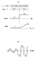
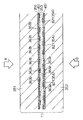
本発明の表示装置は、液晶表示パネルの動画ボケを解決するため、液晶表示パネルの各画素に印加する駆動回路と、バックライトを駆動する駆動回路とを同期をとって画像表示を行う。バックライトユニットにはたとえば10本の蛍光管を並列にならべて配置する。この蛍光管は3〜4本を組みとして順次点灯させ、また、その点灯位置を移動させる。一方、液晶表示パネルの各画素行に印加する(画素電極の電圧を書きかえる)位置も走査する。この走査と蛍光管の点灯とは同期をとる。また蛍光管は、画素に電圧を印加され書きかえられた画素上の液晶層の液晶が十分変化した後に、その画素行に対応する蛍光管を点灯するようにする。
【0014】
このように蛍光管の点灯タイミングと液晶表示パネルへ印加する電圧のタイミングとを同期を取る。つまり、液晶の変化が十分変化した領域にのみバックライトから光を照射し、画素を表示するのである。一方で、画素が表示されない時間が生じる。このためCRTの表示状態と同様の表示状態が実現し動画ボケが改善されるのである。
【0015】
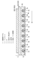
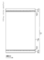
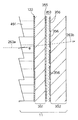
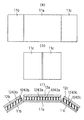
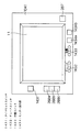
第1図は本発明の表示装置の断面図を示したものである。導光板15はアクリル樹脂,ポリカーボネート樹脂あるいはガラス基板もしくはプリズムシート等から構成される。この導光板15にはスリット状に穴13が複数形成されてあり、これらの穴13にはそれぞれ蛍光管14が挿入されている。蛍光管の太さは2〜3(mm)のものを採用し、導光板15は蛍光管の直径(太さ)よりも2〜3(mm)厚いものを用いる。
【0016】
蛍光管の本数は表示パネル11の大きさに左右されるが、一般的に表示領域を少なくとも3等分、好ましくは8等分以上に分割して表示する必要性があるから3本以上好ましくは8本以上の蛍光管を用いる。また、蛍光管の本数をn(本)とし、表示パネルの有効表示領域の縦幅をH(cm)とすると次式を満足するようにする。
【0017】
【数1】
5(cm)≦H/n≦20(cm)
さらに好ましくは
【0018】
【数2】
8(cm)≦H/n≦15(cm)
の関係を満足するようにする。
【0019】
H/nが小さすぎると蛍光管本数が多くなり高コストになる。一方、H/nが大きすぎると表示領域が暗くなり、また動画ボケが改善されにくくなる。
【0020】
導光板15の背面には反射シート16を配置する。反射シートはフィルム状のもの、あるいは板状のものを用いる。これらはシート等の上にアルミニウム(Al)、銀(Ag)、チタン(Ti)、金(Au)などの金属薄膜を蒸着したものであり、また金属薄膜の酸化を防止するため、金属薄膜の表面にSiO2などの無機材料からなる蒸着膜が形成されている。また、光沢性のある塗料を用いてもよい。その他、誘電体多層膜からなる誘電体ミラーを用いてもよい。
【0021】
ただし、この反射シート16は光を反射するものに限定するものではなく、表面を光拡散する性質のものを用いてもよい。たとえばオパールガラス等の微粉末を塗布したもの、酸化Ti(チタン)の微粉末を塗布したシートあるいは、板が例示される。
【0022】
表示パネル11はOCBモード(Optically Compensated Bend Mode)の液晶表示パネルを用いている。他のTNモード等の液晶表示パネルも用いることができるが説明を容易にするため高速応答のOCBモードまたは、メルク社の高速TN液晶を用いている。ただし、その他、反強誘電液晶を用いてもよい。
【0023】
なお、表示パネル11へは対向基板351側をバックライト12側に向けて配置しても、あるいはアレイ基板352側をバックライト12側に向けて配置してもよい。
【0024】
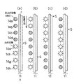
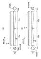
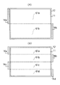
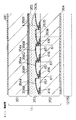
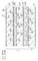
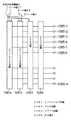
(図1)において、蛍光管14は図中矢印の方向に順次走査をして点灯させる。さらにこの点灯状態の説明を(図4)に示す。(図4)では蛍光管の点灯状態を白色で、また非点灯状態を斜線で示している。図中S矢印で示す位置は液晶表示パネルにおいて画素行の電圧を書きかえている位置を示している。なお、(図4)において紙面上を表示パネルの画面上部と、紙面下を表示パネルの画面下部として、表示パネルの走査は上から下方向とする。もちろん、実際には上下方向と下上方向とを交互に繰り返してもよい。
【0025】
(図4)においては説明を容易にするため、蛍光管14の本数を8本とし、内4本を点灯状態、残りの4本を非点灯状態であるとして説明するが、これに限定するものではなく、2本が点灯状態で、6本が消灯状態でもよく、逆に6本が点灯状態で2本が消灯状態でもよい。また蛍光管の本数は8本以上でもよい。この点灯の本数は表示領域の明るさと動画ボケの改善度合いを考慮して決定すればよい。
【0026】
点灯状態の蛍光管の本数をn1、蛍光管の本数をn0としたとき、実験および評価の結果、以下の条件を満足させることが好ましい。
【0027】
【数3】
(1/4)n0≦n1≦(3/4)n0
さらには、以下の条件を満足させることが好ましい。
【0028】
【数4】
(1/3)n0≦n1≦(2/3)n0
なお、本発明の実施例では発光管14を蛍光管としたがこれに限定するものではなく、EL表示管あるいは、線状の白色LEDあるいはエッジに配置した白色電球、白色LEDを線状の導光板(ファイバー)等で線状に発光領域を有するように構成したものでもよい。つまり、線状に発光領域を有するものであればいずれのものでもよい。
【0029】
また、S矢印位置と蛍光管の点灯位置とは同期をとって駆動を行うが、駆動周期は一般的な表示状態よりも速くすることが好ましい。速くするとは、たとえば一般的に表示パネルは60(Hz)周期で画素の電圧が書き換えられるが、これを60(Hz)以上(たとえば、100Hz)にすることをいう。
【0030】
その理由はフリッカが発生するためである。これはバックライトの点灯状態と液晶の画素の書き換えタイミングにより、微小な偏差が生じるためである。実験および評価の結果、フリッカの発生をなくすためには通常の周期(たとえば、60(Hz))を1Fとした場合、走査周期Fsは以下の条件を満足させるようにすることが好ましい。
【0031】
【数5】
1.2F≦Fs≦3F
さらには、以下の条件を満足させることが好ましい。
【0032】
【数6】
1.5F≦Fs≦2F
一般的には駆動回路の簡単さ、構成の容易さから、
【0033】
【数7】
Fs=2F
とすることが好ましい。もちろん、Fs≧2Fとすることが好ましいのであるが、駆動周波数が高くなると回路部品が高くなってしまう。また、1.5Fなどの駆動周期は、一時的に映像信号データをデジタル化してメモリに記憶する必要がでるため同様にコストが高くなる。
【0034】
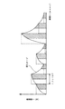
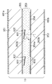
(図4(a))で示すようにS矢印の位置(画面の中央部)の画素行に電圧を印加している。S矢印の位置より画面上部の蛍光管14(14a,14b,14c,14d)は非点灯状態である。S矢印の位置より画面下部の蛍光管14(14e,14f,14g,14h)は点灯状態である。このことから(図4)では任意の画素行には電圧を印加してからFs/2の時間経過後、バックライトの蛍光管が点灯して画像が表示されることになる。
【0035】
各画素に印加された電圧により、液晶層の液晶は電気光学(V−T)特性に対応するように透過率を変化させる。この変化はFs/2時間内に終了する。終了後、バックライトの蛍光管が点灯し観察者に画像として見えるようになる。したがって、液晶が変化している間は画像が表示されず、かつ、この期間は黒表示であるため動画ボケは解消される。
【0036】
この状態をさらに理解を容易にするため、(図2)に説明図を記載する。(図2)において実線が任意の画素液晶の透過率の変化を示している。この場合は任意の画素とは表示領域の上部と考えればよい。理想的には点線のように矩形に変化することが好ましい。しかし、液晶には一定の立ちあがり時間および、立ち下がり時間が必要であるには実線のような透過率曲線となる。
【0037】
透過率曲線において斜線で示した位置(時間)が、バックライトで点灯していることを示している。つまり、液晶の変化が終了した時点で、この画素を照明する位置の蛍光管が点灯する。したがって、斜線部の面積が実効値として観察者に認識される。認識はCRTの表示状態と同様に飛び飛びとなる。
【0038】
なお、このように高速に点滅する蛍光管(灯)はヒューネット(株)、(株)ブライト研究所,市光工業(株)等が開発している。また、蛍光管の発光色は白色光に限定するものではなく、赤(R),緑(G),青(B)等でもよい。これらの発光色の蛍光管をフィールドシーケンシャルに駆動することによりカラー表示を行うことができるからである。発光素子がLEDの場合も同様である。
【0039】
(図4(a))→(図4(b))→(図4(c))→(図4(d))→(図4(a))に示すように点灯する蛍光管の位置は走査され、かつ、表示パネル11を書きかえると画素行位置も走査される。つまり画素に電圧が印加されてから(1/2)Fs後に表示される。もちろんのことながら、点灯する蛍光管の本数により電圧が印加されてから(1/3)Fs後に変更した(2/3)Fs後に変更したりすることができる。
【0040】
一般的に表示パネルを見る環境(室内)が明るいと表示領域を明るくする必要がある。その際は蛍光管の点灯本数を増加させる。表示領域が明るく、かつ室内が明るい場合、動画ボケは見えにくい。一方、環境(室内)が暗いと表示領域の輝度を低下させないと観察者の眼がつかれる。その際は蛍光管の点灯本数を減少させる。表示領域が暗くかつ室内が暗い場合、動画ボケが見えやすい。点灯本数を減少させることにより表示領域が黒表示される期間が長くなるため、動画ボケが改善される。
【0041】
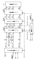
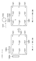
このように蛍光管の点灯本数を変更するには、リモートコントローラあるいは、切り換えスイッチ等を用いて手動で行う他に、(図7)に示すようにホトセンサ71で環境の明るさを自動検出して自動で行ってもよい。ホトセンサとしてはPINホトダイオード、ホトトランジスタ、CdSが例示される。
【0042】
PINホトダイオードあるいは、ホトトランジスタ等のホトセンサ71の出力は、オペアンプ73で増幅される。この際、外光の変化に対して一定の遅延時間を持たせるため、コンデンサC,抵抗Rからなる回路で一定の時定数をもたせる。オペアンプ73の出力は、その出力の大きさに応じて発振回路74で図中丸囲み数字1に示すように、ほとんどで、電圧Eが出力されていない状態から相当の期間電圧Eが出力されている状態の出力に変化する。さらに発振回路74の出力は増幅器75により増幅され蛍光管14のアノード76に印加される。一方、蛍光管14のフィラメント(カソード)77にも電圧Enが印加されており、紫外線光を発生し、蛍光管14は印加電圧Eの実効値に応じて発光する。なお、(図7)は蛍光管は熱陰極方式の場合であるが、冷陰極方式の蛍光管を用いてもよいことは言うまでもない。
【0043】
外光の明るさにより表示領域の輝度を決定するには、(図7)のように単純に外光の明るさだけで決定してもよいが、(図6)に示すように画像の状態(全体的あるいは部分的に明るい映像か、暗い映像か等)に応じて、表示領域の輝度を決定することが好ましい。もしくは外光と画像の状態の両方を考慮して決定する。
【0044】
(図6)において、61は輝度信号(Y信号)によりマッピングされる仮想的な表示領域とする。表示領域61は多数個の表示画素の組にマトリックス状に分離され、各表示画素の組内で演算を行う。その結果をメモリ62に蓄積する。この蓄積結果から輝度分布、所定レベル以上の明るさをもつ画素の個数(明領域個数)あるいは所定レベル以下の明るさの画素の個数等を求め、各求められた結果は乗算器64で重みづけされる。この演算結果は演算処理回路63に送られる。
【0045】
また、表示領域61のデータから画面の全体平均輝度、最大輝度(明るさ)、最小輝度(最も暗い画素)等が算出され、結果は先と同様に乗算器64で重みづけ処理されて、演算処理回路63に送られる。
【0046】
演算処理回路63はこれらの結果を総合的に判断して表示パネル11への転送データを求める。演算処理回路63は時系列的にデータを処理していくとともに、所定の時間内の表示領域のデータから判断して表示パネル11への出力を決定する。たとえば、明るい画素が続き、その間にわずかな期間だけ暗い画面が表示される場合は、表示パネル11への出力データは従前の状態から変化させない(画面の明暗を変化させない)。一方で徐々に暗い画面に変化している場合は、表示パネル11の輝度レベルを徐々に変化させる。また、星空のように暗い画面(たとえば夜空)に少しの輝点(たとえば星)がある場合は、画面全体を暗くするが、画面の1/4以上に領域に白い帯状の画像が表示される場合は画面を明るくする。このような制御は経験的にあるいは画像評価により求めて作製した判断ROMデータを参照して行う。
【0047】
また、判断ROMデータを用いて(図6)に示すような抽出各データへの重みづけ係数を求める。このようにバックライトの輝度制御を行うことにより、奥ゆき感のある映像を表示することができる。
【0048】
また、有機EL,表示パネルFEDなどの自己発光型の場合にも、(図6)(図7)の駆動方式を適用することができる。この場合はまた、ガンマカーブを変化させればよい。動画ボケ対策はCRT以外のディスプレイ、たとえば、PDP,DMD(DLP),ELなどドットマトリックス型の表示パネルに共通に発生するため、以下の事項、方法、装置はドットマトリックス型の表示パネルに共通して適用される。
【0049】
以上のように動画ボケを改善する1つの方法として、画像が見える時間(以後、画像開口時間と呼ぶ)を短くすることである。たとえば、表示パネル等を見える周期を“画像表示−黒表示−画像表示−黒表示……”とすればよい。画像表示をおこなっている時間をT1(sec)とし、黒表示の時間をT2(sec)とした時以下の条件を満足させることが好ましい。
【0050】
【数8】
0.3 ≦ (T1/(T1+T2))≦ 0.8
さらに好ましくは、以下の条件を満足させる。
【0051】
【数9】
0.4 ≦ (T1/(T1+T2))≦ 0.6
(T1/(T1+T2))の値が小さくなると、画像が暗くなりすぎる。一方、大きくなると、動画ボケは改善されない。
【0052】
(図5)は、赤(R),緑(G),青(B)発光の蛍光管をフィールドシーケンシャルに点灯させることにより、カラー表示を行う場合の説明図である。表示パネル11はモノクロ表示パネルを用いる。(図5(a))は従来のフィールドシーケンシャルの場合である。バックライトは常時点灯状態である。(図5(b))は本発明の点滅型のバックライトを使用した実施例である。斜線部が点灯状態である。1フィールド期間内にR,G,Bの3つの表示が行われ、それぞれ(R,G,B)の一部の期間の間にバックライトが点灯する。もちろん、蛍光管の点灯位置は走査する。
【0053】
なお(図1)において、導光板15の穴13に蛍光管14を挿入するとしたが、これに限定するものではなく、(図3)に示すように導光板15と蛍光管14とを一体として形成してもよく、また、板状の蛍光管を形成し、板状の各部が線状に発光するように構成してもよい。その他(図1)の穴13に蛍光管14を挿入し、穴を樹脂もしくはゲル等の光結合剤122で充填してもよい。充填を行うことにより光利用効率の向上を行うことができる。
【0054】
また、(図3)に示すように導光板15の光出射面にプリズムシート32および、前記プリズムシート32の出射面にプリズムのレンチをめだちにくくする拡散シート31を配置してもよい。プリズムシートは住友3M社が販売しており、また拡散シートは(株)キモトが販売しているライトアップシリーズを用いればよい。
(実施の形態2)
以上はバックライトの点灯状態を改良することにより動画ボケを改善する方法であった。この方法に加えて液晶の応答性を改善する駆動方法を採用することが好ましい。以下、その駆動方法について(図8)および(図9)を用いて説明をする。
【0055】
(図8)は従来の液晶表示パネルの駆動方法の説明図である。(図8)において、Fx(ただし、xは整数)はフィールド番号、Dx(ただし、xは整数)はソース信号線に印加する電圧に相当するデータ(以後、電圧データと呼ぶ),Vx(ただし、xは整数)は前記電圧データにより作られ、ソースドライブ回路からソース信号線に出力される電圧、Tx(ただし、xは整数)は画素201に前記電圧が印加されることにより液晶の透過率が変化し、前記電圧に対応する状態になったときの光の透過量である。
【0056】
本明細書では説明を容易にするために添え字xが大きいなどフィールドFxは光のフィールドであること、電圧データDxは値が大きいこと、印加電圧Vxは電圧が高いこと、透過量Txは透過量が大きいことつまり液晶の透過率が高いことを示すものとする。ただし液晶への印加電圧と透過量との関係は非線形特性を示すため透過量Txの添え字の大きさと実際の透過量とは比例しない。
【0057】
なお、(図8(a))では印加電圧Vxは、理解を容易にするために絶対とであらわしたが、液晶は交流駆動する必要があるため、(図8(b))で示すように1フィールドごとに対向電圧を中心に正および負極性の電圧を印加している。以上のことは以下の図面に対しても同様である。
【0058】
以下、1つの画素に注目して説明する。ソースドライブ回路は入力されるアナログ信号をサンプルホールドして電圧データDxを作成する。また前記ICは前記電圧データDxを一走査線線分保存し、ゲートドライブ回路と同期をとりソース信号線に印加する電圧Vxを出力する。今、フィールドで注目している画素(以後、単に画素と呼ぶ)への電圧データD1からD5に変化したとする。するとソースドライブICは電圧V5をソース信号線に出力し、前記電圧はゲートドライブICと同期がとられ画素に入力される。
【0059】
しかしながら、フィールドF4では、前記電圧V5が印加されても前記電圧V5に相当する所望値の透過量T5にならず、通常2〜3フィールド以上遅れて所望値のT5になる。これは液晶の立ちあがり速度つまり電圧を印加してから所望値の透過量になるまでの応答時間が遅いためである。
【0060】
(図9)は液晶の応答時間を改善する駆動方法の説明図である。(図9)では(図8)と同様に補正前の電圧データがフレーム番号F4でD1からD5に変化している場合を示している。
【0061】
(図9)ではフィールド番号F3のフィールドメモリの電圧データとフィールド番号F4のフィールドメモリの電圧データを順次比較し、たとえば、(図8)で示すように立ちあがり時間が遅いと、演算器が判定した場合はデータ補正器に信号を送る。データ補正器は前記信号にもとづきフィールド番号F4のフィールドメモリの前記画素の電圧データを補正する。この場合、フィールド番号F4の電圧データは前記電圧データD5よりも大きいデータ、つまりD7補正される。なお前記補正データはあらかじめ実験などにより定められている。
【0062】
以上の処理によって、電圧データは(図9)の補正電圧データ欄のようになる。前記データは順次D/A変換され、ソースドライブ回路に送られ、前記回路により(図9)の印加電圧が画素に印加される。フィールド番号F4で電圧V7が印加され、液晶は急激に立ちあがり、1フィールド時間内で定常透過量T5になる。以上のように電圧データを補正することにより、液晶の立ちあがり時間つまり応答速度は改善され、画像の尾ひきのない映像が得られる。
(実施の形態3)
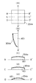
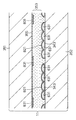
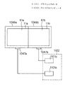
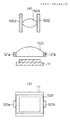
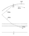
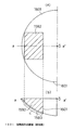
(図1)は3本以上の蛍光管を用いる方法であったが、(図10)に示すように2本の蛍光管14を用いても動画ボケを改善する表示装置を構成できる。(図10)は断面図である。
【0063】
(図10)は導光板15に特徴がある。導光板15は、中央部Aを中心としてくさび型あるいは、円弧状あるいはプリズム形をした二つの導光板15aおよび15bがつなぎあわさった形状をしている。導光板15aの部分の一端には蛍光管14aが配置され、蛍光管14aは主として導光板15aの部分を照明する。一方、導光板15bの部分の一端には蛍光管14bが配置され、蛍光管14bは主として導光板15bの部分を照明する。なお、図中にて2つの導光板15aと15bとが重なる部分Kは、滑らかに円弧状あるいは平面状に形成され、導光板15aと15bとの継ぎ目が目だたないように構成されている。
【0064】
蛍光管14aおよび14bの周囲はそれぞれ反射シート101aおよび101bで取りかこまれ、蛍光管14aおよび14bのから放射された光が効率よく導光板15に入力されるように構成されている。反射シート101aおよび101bとして商品名シルバーラックスなどがある。
【0065】
導光板15の表面にはプリズムシート32を配置するか、もしくは、直接導光板15をプレス加工を行うことにより、プリズム形状を形成する。この方がコストが安くなる。
【0066】
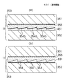
(図11)はバックライトの駆動方法の説明図である。図中S字にて指示する矢印は、(図4)の場合と同様に、映像信号を画素行に書き込んでいる位置を示している。(図11(a))は蛍光管14bが点灯状態であり、(図11(b))は蛍光管14aが点灯状態である。蛍光管14aと14bとは交互に、つまり、駆動周期Fsの1/2の期間点灯する。
【0067】
(図11(a))に示すように蛍光管14bが点灯している。つまり導光板15bが照明されている。その時には導光板15a上の表示パネル11の表示領域に画像が書き込まれている。
【0068】
(図11(b))では蛍光管14aが点灯している。つまり、導光板15aが照明されている。その時には導光板15b上の表示パネル11の表示領域61上に画像が書き込まれている。この状態をさらに詳しくすれば(図12)のようになる。(図12(a))には(図11(a))が対応し、(図12(b))には(図11(b))が対応する。照明領域は導光板15aまたは15bの領域よりも広くなる。そのため導光板の境目が目だたなくなる。
【0069】
以上のように蛍光管14aと14bを交互に点灯させる構成にすることにより、蛍光管を駆動するインバータ回路が小型化になり、かつ、低コスト化を実現できる。
【0070】
以上は、蛍光管14を用いる方式であったが、蛍光管14等の発光部は(図13)に示すように白色LED(light emitting diode)121を用いても構成することができる。白色LEDは日亜化学(株)がGaN系青色LEDのチップ表面にYAG(イットリウム・アルミニウム・ガーネット)系の蛍光体を塗布したものを販売している。その他、住友電気工学(株)が、ZnSe材料を使って製造した青色LEDの素子内に黄色に発光する層を設けた白色LEDを開発している。なお、発光素子として白色LEDに限定するものではなく、たとえばフィールドシーケンシャルに画像を表示する場合は、R,G,B発光のLEDを1つまたは複数のLEDを用いればよい。
【0071】
(図13)は白色LED等を発光素子14として用いた表示装置の断面図である。また、(図14)はバックライト12の表面図である。導光板15aのエッジ部にLEDアレイ141a,141bを光結合層122で取り付けたものである。光結合層122としては、サルチル酸メチル,エチレングリコール、アルコール,水等の液体,フェノール樹脂,アクリル樹脂,エポキシ樹脂,シリコン樹脂,低融点ガラス等の固体が例示される。光結合層122はLED121等が発生する光をよりよく導光板15aに導入するためのものである。光結合層122の透明材料は、屈折率が1.38以上1.55以下のものであれば、ほとんどのものを用いることができる。
【0072】
白色LED121には色むらが発生しやすい。その対策として光結合層122に光拡散剤を添加することは、色むら発生の抑制に効率がある。拡散剤によってLEDから発生する光が散乱するからである。拡散剤の添加とはTiあるいは、酸化Tiの微粉末を添加すること、あるいは、光結合層122の屈折率を異なる物質(あるいは液体)を混入させることにより白濁させることを言う。
【0073】
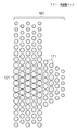
(図14)に示すようにLED122はアレイ状に形成される。またLEDアレイ141の裏面等には、金属板からなる放熱板(図示せず)が取りつけられている。LEDは比較的発熱量が大きいためである。
【0074】
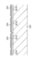
導光板15aは(図15)に示すように、多数のファイバー151が密集されて板状に形成されたものである。ファイバー151はガラスファイバーあるいは樹脂ファイバーが用いられる。ファイバー151は接着剤152でかためて板状にすることが好ましい。
【0075】
このように、ファイバー151で形成された導光板15aを用いることにより、LED121から発生した光はファイバー151に伝達されて線状の発光光源となる。なお、(図14)ではLEDアレイ141aと141bの2つを用いると図示したが、これに限定するものではなく、1つでも、また3つ以上でもよい。
【0076】
LEDアレイ141のLED121は(図4)に示す実施の形態と同様に、一部のLEDが点灯するとともに点灯位置は走査される。そのため、(図1)の表示装置と同一の表示状態(駆動状態)を実現できる。したがって(図1)のように棒状の蛍光管を用いずともドット状のLEDを用いても動画ボケを改善できる。
【0077】
ドット状のLED121を用いる場合、LED121の近傍は発光輝度が高く、この発光輝度のムラが表示パネル11を介して見えることがある。つまり、照明光のムラが発生するのである。この対策を(図16)に示す。導光板15の表面あるいは表示パネル11と導光板15間に配置したシート上に、光拡散部161を形成または配置する。光拡散部とは本来の光を拡散して表示パネル11に到達する光を減少させる機能を有するものの他、金属膜などで直接光を遮光して表示パネル11に到達する光を減少させるものが含まれる。
【0078】
光拡散部161は、(図16)に示すようにLED121の近傍にあるものは円弧状に大きく形成し、LED121から離れた位置にあるものは小さく形成する。また、光拡散部はスモークガラスのように全体にわたり光透過、あるいは光直進率を低下させる構成でもよいが、(図17)のように光拡散ドット171を形成する構成の方が好ましい。光拡散ドット171は、その大きさをLED121に近いところは大きく、遠いところは小さくなるように形成する。このように光拡散部161を形成することにより、バックライト12の照明光は全領域にわたり均一となる。
【0079】
なお、(図16)の構成は発光素子14としてLED121を用いる場合を例にあげて説明したが、これに限定するものではなく、(図11),(図1)のように蛍光管等の他の発光素子14を用いる場合にも適用できることは言うまでもない。つまり、発光素子14の近傍に光拡散部を形成または配置するという技術的思想は他の構成でも適用できる。たとえば、蛍光管であり、オプトニクス(株)が製造しているルナシリーズ等の蛍光球である。その他、東北電子(株)も同様の蛍光球を販売している。
【0080】
(図18)はLED121のかわりに、バックライト12の側面に棒状の蛍光管あるいは、EL素子を用いる場合である。(図18(a))は表示領域61aを照明する蛍光管14aをバックライト12の左上端に配置し、表示領域61bを照明する蛍光管14bをバックライト12の右下端に配置した例である。蛍光管14aと14bとは交互に点灯する。なお、交互とは完全に蛍光管14aが点灯している期間は蛍光管14bが消灯していることを意味するものではなく、蛍光管14aと14bの両方が点灯している期間あるいは、蛍光管14aと14bの両方が消灯している期間があってもよい。
【0081】
(図18(b))は4本の蛍光管を交互にバックライト12のエッジ部に配置する構成である。蛍光管14aは表示領域61aを照明し、蛍光管14bは表示領域61bを照明し、蛍光管14cは表示領域61cを、蛍光管14bは表示領域61dを照明する。蛍光管14は14a→14b→14c→14d→14a→と点灯させる。あるいは14a,14b→14c,14d→14d,14a→14b,14c→と2本ずつの組で順次点灯させる。
【0082】
なお、蛍光管14あるいはLED121の点灯は順次走査することに限定するものではなく、(図19)に示すように同時に複数(図19では2つ)の領域を点灯し、この点灯状態(図19(a))と(図19(b))の状態を交互に切り換えてもよい。
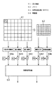
(実施の形態4)従来の透過型の表示パネルの1画素はR,G,Bの3色のカラーフィルタで形成されている。本発明の表示パネル、表示装置の1画素は(図20)に示すようにR,G,BとY(イエロー)のカラーフィルタを有する。Yのカラーフィルタを用いるのは表示画像の階調性を向上させるためである。たとえば、赤(R)いバラの花を人間が見ると、日光があたっている部分の赤は黄色がかかって見え、影になっている部分は青みがかかって見える。この状態を良好に再現しようとするとR,G,Bの3原色では良好に再現することができない。微妙なY(イエロー)の表示ができないからである。(図20)の一画素はR,G,B,Yの4つの色のカラーフィルタを具備する。(図6)に示す映像信号処理方法を用いてY表示をする箇所を求めてY表示を行う。
【0083】
(図20(a))は光の分光分布を長波長側からR→Y→G→Gと順に配置した実施例であり、(図20(b))は正方格子で構成した例である。また(図20(c))は高輝度表示に寄与するGのフィルタの面積を大きくした例である。また、(図20(d))はYのフィルタをR,G,Bのフィルタに比較して小さく構成した実施例である。その他(図21(a))に示すように同心円状に形成してもよく、また(図21(b))のように構成してもよい。
【0084】
(図22)はR,G,B,Yの4色を有する表示パネルに画像を表示するための駆動回路のブロック図である。
【0085】
映像信号はRGB信号変換ブロック221に入力される。同時に水平同期信号(HS),垂直同期信号(VS)が入力される。RGB信号変換ブロック221はマトリック変換し、赤(R),緑(G)および青(B)の8bitデジタルデータを出力する。このR,G,Bデータは次段のガンマ処理ブロック223に入力される。
【0086】
本発明の表示パネルはR,G,Bの画素の他にY(イエロー)の画素(カラーフィルタ)を有するため、Yデータ作成ブロック222でYデータを作成する。YデータはRデータ8bitとGデータ8bitから作成する。具体的にはR,Gデータを加えて平均もしくはRもしくは、Gデータを重みづけ平均し求める。求めたYデータは8bitデータとして次段のガンマ処理ブロック223に入力される。
【0087】
ガンマ処理ブロック223に入力された、R,G,BおよびYデータはROMテーブル(図示せず)で液晶の電気−光学的特性に適し、かつ、リニアに階調特性が変化するようにデータ変換される。出力データは9bitデータとなる。
【0088】
また、ガンマ処理ブロック223からデータはオフセット処理ブロック224に入力される。オフセット処理ブロックは液晶の立ちあがり電圧を加算する。通常立ちあがり電圧は1.2(V)〜1.8(V)である。
【0089】
オフセット処理ブロック224を出力した9bitデータは反転処理ブロック225に入力される。入力データは反転処理ブロック225に入力され、1フレーム(1F)もしくは、1水平走査期間(1H)毎に反映する映像データとなる。映像データは反転するとしてもMSBを“0”に、反転しない場合はMSBを“1”として処理され、10bitデータとして出力される。
【0090】
反転のタイミング信号はVD,HDパルスと、ユーザが行う駆動方式選択スイッチ(図示せず)で行う。駆動方式としては、フィールドごとに画素に印加する映像信号の極性を反転させる1F反転駆動,1水平走査期間ごとに映像信号の極性を反転させる。1H反転駆動,水平の1ドットごとに映像信号の極性を反転させる1カラム(C)反転駆動,上下左右の1ドットごとに画素に印加する映像信号の極性を反転させる1ドット(1D)反転駆動がある。本発明では、フリッカおよび輝度傾斜の発生を防止するため1D反転駆動を採用している。
【0091】
反転処理ブロック225から出力された映像データはD/A回路でD変換されてアナログデータとなり、表示パネル11に印加される。
【0092】
ここで重要なのは観察者が自由にNBとNWモードとを切り換えられる点である。表示パネル11への光入射状態,表示パネル11の観察方向により最適に表示画像が見えるようにNBとNWモードとを切り換える。当然のことながら、観察者の眼の位置、入射光の方向をホトセンサ等で自動検出し、自動的にNWモードとNBモードとを切り換えてもよい。このことは表示パネルが反射であろうと透過であろうとどちらでも適用できる。以上の制御は制御ブロック226で行う。
【0093】
ガンマ処理ブロック223についてさらに詳しく説明しておく。(図23)はノーマリホワイト(NW)モードでのガンマカーブを示している。実線が通常状態でのガンマカーブである自然な映像表示とするには、実際の自然色(本来の色)ではなく、記憶色あるいは人間の眼の特性(プレキンエ現象,対比現象等)を考慮して色再現を行う必要がある。一般的に明るい赤は朱色(黄みの赤)に表示することが好ましい。また黒は青紫ぎみに表示することが好ましい。
【0094】
これを実現するため、ガンマカーブを変化させる必要がある。(図6)の回路を用いて、まず映像の特徴を抽出する。明るい赤の箇所が存在すると、この箇所の色を黄みにする必要がある。そのためY(イエロー)色の画素を点灯させるために画像データ(図22)の回路で作成する。もしくは、G色のガンマカーブを(図23)の点線のように変化させて赤に緑を加える。もしくは、赤色のガンマカーブを(図23)の一点鎖線のように変化させる。暗い黒の箇所が存在すると、この箇所の色を青みにする必要がある。そのため、青のガンマカーブを(図23)の点線のように変化させる。これらのガンマカーブの変化は各画素あるいはエリアごとに行い処理する。
【0095】
より良好な色再現を行うためには、(図24)に示すようにR,G,B,Y画素に加えてP(紫)色の画素を形成すればよい。もしくは、R,G,Bの3原色に加えて、P(紫)の画素を形成あるいは配置すればよい。R,G,BとPの配置は(図24(a))のようにストライプ状に配置する構成が例示される。また(図24(b))のように配置してもよい。(図24(b))はRとG、GとP、BとYの組が心理補色の関係になっている。そのため色再現を良好にできる。
【0096】
P(紫)のデータを作成するのは容易であって、(図25)のようにRデータとBデータからPデータを作成するPデータ作成ブロック227を付加すればよい。その他の構成は(図22)と同様であるので説明を省略する。
【0097】
なお、(図20)(図21)あるいは(図24)で説明したR,G,Bの3原色意外のカラーフィルタ(色)を有する構成は液晶表示パネルに限定されるものではなく、PDP(プラズマディスプレイパネル),ELパネル,FPDなどの自己発光型表示パネルにも適用できる。発光色がR,G,B,Y等とすれば実現できるからである。
【0098】
また、(図22),(図25)に示す駆動回路および駆動方法も同様に自己発光型表示パネルにも適用できることは言うまでもない。ただし、各表示パネルにはオフセット処理ブロック、反転処理ブロックが必要ない場合もある。したがって本発明の技術的思想はYデータ作成ブロック222等を具備することである。(実施の形態5)
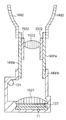
(図1)等の表示パネルは複数の発光素子14を用い、かつ、これらを順次点灯するという走査を行うことにより画像を表示するものであった。(図26)は1つの発光素子14(発光管等)を用いて表示装置の一部を点灯状態にし、画像を表示するものである。
【0099】
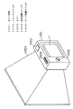
発光素子14は反射鏡262により一方向にのみ照明されるようにされている。またこの反射鏡は点0を中心として角度θの範囲を回転するように構成されている。この回転はパルスモータを用いることによって容易に実現できる。その他、レーザプリンタ等に用いられているガルバノミラーを用いても、これらが容易に実現できるであろう。ここでは説明を容易にするには反射鏡を回転するとして説明をする。
【0100】
(図26)において、261はミラーであり、表示パネル11の中央部を水平にされ、このミラーを中心として上、下方向のミラーは一定の角度をもって配置されている。ミラーは発光素子14から放射された光線263aを反射して光線263bとし、この光線263bを表示パネル11に垂直にもしくは、所定の角度をなすように入射するようにする。ミラー261の角度は263bの入射角度を一定にするように設定されている。
【0101】
反射鏡263が回転することにより、入射光263aはミラー261aに入射する。この入射光263aによりAの部分が照明される。拡散板32は入射光263aのムラを均一にして表示パネル11に入射する。次に入射光263aはミラー261bに入射しBの領域を照明する。次に入射光261cに入射し、Cの領域を照明する。以上のように反射鏡が回転するにつれて、表示パネル11の照明領域が変化する。つまり、この表示状態は(図1)の蛍光管14が順次点灯している状態と相似する。ミラー261kに入射した後はブランキング時間であり、このブランキング時間の間に反射鏡262は高速に回転し、ミラー261aの位置までもどり、再びミラー261aから順次入射光263aを入射させるようにする。このような動作を行うことにより表示パネル11の上面から順次画像が表示されるように構成できる。なお、画素行を書きかえるS点については(図4)で説明した事項と同様であるので説明を省略する。
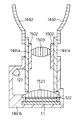
【0102】
(図26)の実施例は主として直視タイプの表示装置の実施例である。この技術的思想は、投射型表示装置にも適用することができる。(図27)は投射型表示装置の構成図である。(図27)においてMは(図26)に示した表示装置に相当するものである。しかし、投射型表示装置の場合は拡散板32は必要性がない。また発光素子14としてはメタルハライドランプ,超高圧水銀灯,ハロゲンランプ,キセノンランプ等の放電灯を用いる。表示パネル11からの光はフィールドレンズ272で集光され、投射レンズ271でスクリーン(図示せず)に拡大投影される。この(図27)の構成を採用することにより動画ボケの発生はなくなり、良好な画像表示を実現できる。
【0103】
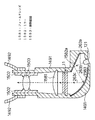
その他、直視表示パネル、携帯情報端末,パーソナルコンピュータ,電子カメラのモニター,ビデオカメラのモニター、投射型表示装置等の表示装置にも(図26)の技術的思想は適用できる。(図28)はその実施例の斜視図である。また(図30)は断面図である。発光素子14は棒状の蛍光管を用いる。(図30)に示すように反射鏡262を回転することにより、光263aが発生し、前記入射光263aは反射フレネルレンズ282に入射する。反射フレネルレンズ282により入射光は平行光に変換され、表示パネル11を照明する。
【0104】
表示パネル11は反射型の画素を有する反射型表示パネルである。また、反射フレネルレンズ282は反射面鏡をフレネルレンズ状に形成したものである。金属板を切削加工することにより、また、プレス加工したアクリル等の樹脂板に金属薄膜を蒸着したものが例示される。もちろんフレネルレンズでなくても放物面鏡でもよい。また、放物面鏡でなくともたとえば、だ円面鏡でもよい。
【0105】
表示パネル11と反射フレネルレンズ(放物面鏡)との位置関係は(図29)のようになる。放物面鏡の焦点位置Pに発光素子14が配置されている。またフレネルレンズは3次元状のものでも2次元状のものでもよい。発光素子14が点光源の場合は、3次元状のものを採用する。発光素子14から放射された光263aは放物面鏡291で平行光263bに変換される。変換された光263bは表示パネル11に角度θで入射する。この角度θは設計の問題であり、反射光263cが最も観察者に見やすいように(あるいは最も観察者の目に到達しないように)される。
【0106】
反射フレネルレンズ282は、ふた285に取りつけられており、表示パネル11は本体281に取りつけられている。ふた285は回転部286で自動に傾きを変更できる。ふた285をおりたたむことにより突起283と留め部284とが結合し、ふた283は表示パネル11および反射フレネルレンズ282を保護する。また留め部284にスイッチが構成されており、ふた282をあけると自動的に発光素子14が点灯し、また表示パネル11が動作するように構成されている。
【0107】
本体281には切り換えスイッチ(ターボスイッチ)が取りつけられているターボスイッチ281はノーマリブラックモード表示(NB表示)とノーマリホワイトモード表示(NW表示)とを切り換える。これは表示パネルとして反射型の高分子分散液晶表示パネルを用いる場合に特に有効になる。
【0108】
通常の明るさの外光の場合はNWモードで画像を表示する。NWモードは広視野角表示を実現できる。非常に外光に弱い場合に用いる。液晶層が透明状態のとき画素電極に反射した光を直接観察者が見ることになるため、表示画像を明るく見ることができる。視野角は極端に狭い。しかし、外光が微弱な場合でも表示画像を良好に見ることができるのでパーソナルユースで使用し、かつ短時間の使用であれば実用上支障がない。一般的にNBモード表示は使用することが少ないため、通常はNW表示とし、ターボスイッチ287を押さえつづけているときにのみNBモード表示となるように構成する。
【0109】
(図28)の表示装置の特徴として、ガンマ切り換えスイッチ288を装備している点がある。ガンマ切り換えスイッチ288はガンマカーブを1タッチで切り換えできるようにしたものである。これは白熱電球の照明下では表示パネルに入射する入射光の色温度は4800K程度の赤みの白となり、昼光色の蛍光灯で7000k程度の青み白となり、また屋外では6500k程度の白となる。したがって、(図28)の表示装置を用いる場所によって表示パネルの表示画像の色が異なる。特にこの違和感は蛍光灯の照明下から白熱電球の照明下に移動した時に大きい。この時にガマン切り換えスイッチ288を選択することにより正常に表示画像を見えるようにできる。
【0110】
ガンマ切り換えスイッチ288aは、白熱電球の光で良好な白表示となるように赤のガンマカーブを液晶の透過率(変調率)が小さくなるようにしている。288bは昼光色の蛍光灯に適用するように青の透過率(変調率)を小さくなるようにしている。288cは太陽光の下で最も良好な日表示となるようにしている。したがってユーザはガンマ切り換えスイッチ288a,288b,288cを選択することによりどんな照明光のもとでも良好な表示画像を見られる。
【0111】
発光素子14から放射される光263aは反射型フレネルレンズ282の一部を帯状に照明し、この照明された光は平行光に変換されて表示パネル11を帯状に照明する。したがって、この場合も(図26)あるいは(図4)の表示方法を実現できることになる。
【0112】
発光素子14が点光源の場合は、(図31(a))のように配置すればよい。点光源14が複数の場合は(図31(b))のように配置すればよい。なお、(図31(c))のように反射フレネルレンズ282は282aと282bのように複数の部分にしてもよい。
【0113】
(図32)は(図28)のように表示パネル11の表示領域を帯状に照明するものではなく、1つの発光素子を固定し、この発光素子14からの光を凸レンズで平行光に変換して表示パネル11を照明するものである。
【0114】
凸レンズとしてフレネルレンズ321を用い、フレネルレンズ321の平面側を発光素子14側に向けている。これは正弦条件を良好なものとするためである。フレネルレンズ321は表示パネル11上に直接あるいは間接的に配置している。また、フレネルレンズ321の中心の中心Pはふた283側によせている。この状態を(図33)に示す。観察者の眼322は表示パネル11の表示画像を斜め方向から見る。
【0115】
表示パネル11への光線の入射角度は、ふた283を回転中心286を中心として回転させて調整する。この構成により表示パネル321に良好な狭指向性の光が入射させることができる。
【0116】
また、(図34)は本発明の他の実施例における表示装置の構成図である。表示パネル11としては、TN液晶表示パネル等の偏光方式の表示パネル11を用いる。表示パネル11は入射側および出射側に偏光フィルム349を配置する。
【0117】
(図34)の導光板は中部が空調となっている。空調341はアクリル樹脂等の樹脂成型した箱342(バックライトケース)あるいは、ガラス基板を用いて構成する。バックライトケース342の中部を空調341(空間)にしているため軽量化することができる。バックライトケース342の裏面には反射シート16が取り付けられ、表面にはストライプ状の反射膜343が形成されている。
【0118】
発光素子14からの光はバックライトケース342内で乱反射をくりかえし、伝達される。バックライトケース342で乱反射した光は開口部462から出射する。つまり開口部462もストライプ状である。
【0119】
偏光変換板345は入射光263aを偏光変換して出射する。偏光変換345は入射光263aをP偏光またはS偏光に分離する誘電体多層膜からなる偏光分離層347と、分離された偏光を反射するミラー348および偏光の位相角を回転し、P偏光をS偏光に変換する位相フィルム346を有する。
【0120】
ここでは説明を容易にするため偏光分離膜はS偏光を透過し、P偏光を反射するとし、位相フィルム346はP偏光をS偏光に変換するとして説明する。
【0121】
バックライトケース342は表面にストライプ状の反射膜343、裏面に反射シート(もしくは光拡散シート)16が配置もしくは直接蒸着などの製造方法を用いて形成されている。そのため開口部462からのみ光を出射する。バックライトケース342から出射した光263aは、偏光変換板345に入射し、偏光分離膜347でP偏光が反射し、光263cとなる。この光263cは位相フィルム346で位相が90度(DEG.)回転させられ、光263dつまりS偏光となる。一方、偏光分離膜347を透過したS偏光263bはそのままプリズム板32aに入射する。同様にS偏光263dもプリズム板32aに入射する。
【0122】
以上のようにバックライトケース342から出射された光263aはすべてS偏光となるため光利用効率が従来に比較して倍になる。なお、プリズム32bは表示パネル11に入射する光の指向性を高めるために用いるものであり必須なものではない。また、拡散シートはS偏光263bと263dとの境目を目だちにくくするものである。
【0123】
次に、(図35)に示す表示装置はバックライト12に特徴がある。バックライトを構成する導光板15の裏面には反射シートが配置され、表面にはストライプ状に形成された誘電体多層膜からなるカラーフィルタ(以後、誘電体カラーフィルタと呼ぶ)を、形成したものである。誘電体カラーフィルタは別途他の透明基板上に形成し、この基板を導光板15に取り付けてもよい。
【0124】
誘電体カラーフィルタ357は、画素ピッチに同一あるいは相似する幅に形成されストライプ状である。誘電体カラーフィルタ357は誘電体膜を多層に形成することにより、赤(R),緑(G)あるいは青(B)の光を透過もしくは、反射するようにしたものである。その他;R,G,Bの3原色の他にY(イエロー),シアン,マゼンダ等の誘電体カラーフィルタでもよく、また、これらとR,G,Bの誘電体カラーフィルタとの両方もしくは任意の1つを用いてもよい。
【0125】
誘電体カラーフィルタ122と表示パネル11の基板間は光結合層122を用いて接着することにより、位置ずれが発生せず、また不要なハレーションの発生を防止できる。
【0126】
誘電体カラーフィルタ347R,347Bは347GはG光のみを透過する。347BはB光のみを透過するとして説明をする。ここでは347RはR光のみを透過する。
【0127】
誘電体カラーフィルタ347は、特定の光(R,G,B)を選択して透過し、他の光を導光板15内に反射する。したがって、樹脂からなるカラーフィルタのように光吸収が発生しないから、光利用効率が高い。つまり、発光素子14が発生する白色光をほとんどロスなしに、R,G,B等の光に分離して利用することができる。
(実施の形態6)
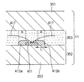
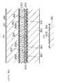
ここで、液晶表示パネルについて説明をしておく。(図35)において352は画素電極354等がマトリックス状に形成された基板(以後、アレイ基板と呼ぶ)、351は対向電極355が形成された基板(以後、対向基板と呼ぶ)である。なお、対向基板とはスイッチング素子等が形成された基板の対向に位置する基板の意味であり、対向電極355の形成の有無に左右されない。また、対向電極355もしくは、画素電極354にはカラーフィルタ356が形成される。通常このカラーフィルタはゼラチン樹脂,アクリル系樹脂に染料あるいは、顔料を添加することにより形成される。
【0128】
対向基板351とアレイ基板352間に液晶層を挟持させる。液晶層353として、TN液晶,STN液晶,強誘電液晶,反強誘電液晶,ゲストホスト液晶,コレステリック液晶、スメクティック液晶、または高分子分散液晶(以後、PD液晶と呼ぶ)が用いられる。特に光利用効率の観点からPD液晶を用いることが好ましい。
【0129】
PD液晶材料としてはネマティック液晶が好ましく、単一もしくは2種類以上の液晶性化合物や液晶性化合物以外の物質も含んだ混合物であってもよい。
【0130】
なお、先に述べた液晶材料のうち、異常光屈折率neと常光屈折率noの差の比較的大きいシアノビフェニル系のネマティック液晶、または、経時変化に安定なトラン系、クロル系のネマティック液晶が好ましく、中でもトラン系のネマティック液晶が散乱特性も良好でかつ、経時変化も生じ難く最も好ましい。
【0131】
樹脂材料としては透明なポリマーが好ましく、ポリマーとしては、製造工程の容易さ、液晶相との分離等の点より光硬化タイプの樹脂を用いる。具体的な例として紫外線硬化性アクリル系樹脂が例示され、特に紫外線照射によって重合硬化するアクリルモノマー、アクリルオリゴマーを含有するものが好ましい。中でもフッ素基を有する光硬化性アクリル樹脂は散乱特性が良好なPD液晶層353を作製でき、経時変化も生じ難く好ましい。
【0132】
また、前記液晶材料は、常光屈折率n0が1.49から1.54のものを用いることがこのましく、中でも、常光屈折率n0が1.50から1.53のものを用いることがこのましい。また、屈折率差△nが0.20以上0.30以下のものとを用いることが好ましい。n0,△nが大きくなると耐熱、耐光性が悪くなる。n0,△nが小さければ耐熱、耐光性はよくなるが、散乱特性が低くなり、表示コントラストが十分でなくなる。
【0133】
以上のことおよび検討の結果から、PD液晶の液晶材料の構成材料として、常光屈折率n0が1.50から1.53、かつ、△nが0.20以上0.30以下のトラン系のネマティック液晶を用い、樹脂材料としてフッ素基を有する光硬化性アクリル樹脂を採用することが好ましい。
【0134】
このような高分子形成モノマーとしては、2−エチルヘキシルアクリレート、2−ヒドロキシエチルアクリレート、ネオペンチルグリコールドアクリレート、ヘキサンジオールジアクリート、ジエチレングリコールジアクリレート、トリプロピレングリコールジアクリレート、ポリエチレングリコールジアクリレート、トリメチロールプロパントリアクリレート、ペンタエリスリトールアクリレート等々である。
【0135】
オリゴマーもしくはプレポリマーとしては、ポリエステルアクリレート、エポキシアクリレート、ポリウレタンアクリレート等が挙げられる。
【0136】
また、重合を速やかに行う為に重合開始剤を用いても良く、この例として、2−ヒドロキシ−2−メチル−1−フェニルプロパン−1−オン(メルク社製「ダロキュア1173」)、1−(4−イソプロピルフェニル)−2−ヒドロキシ−2−メチルプロパン−1−オン(メルク社製「ダロキュア1116」)、1−ビドロキシシクロヘキシルフェニルケトン(チバガイキー社製「イルガキュア184」)、ベンジルメチルケタール(チバガイギー社製「イルガキュア651」)等が掲げられる。その他に任意成分として連鎖移動剤、光増感剤、染料、架橋剤等を適宜併用することができる。
【0137】
なお、樹脂材料が硬化した時の屈折率npと、液晶材料の常光屈折率noとは略一致するようにする。液晶層353に電界が印加された時に液晶分子(図示せず)が一方向に配向し、液晶層353の屈折率がnoとなる。したがって、樹脂の屈折率npと一致し、液晶層353は光透過状態となる。屈折率npとnoとの差異が大きいと液晶層353に電圧を印加しても完全に液晶層353が透明状態とならず、表示輝度は低下する。屈折率npとnoとの屈折率差は0.1以内が好ましく、さらには0.05以内が好ましい。
【0138】
PD液晶層353中の液晶材料の割合はここで規定していないが、一般には40重量%〜95重量%程度がよく、好ましくは60重量%〜90重量%程度がよい。40重量%以下であると液晶滴の量が少なく、散乱の効果が乏しい。また95重量%以上となると高分子と液晶が上下2層に相分離する傾向が強まり、界面の割合は小さくなり散乱特性は低下する。
【0139】
PD液晶の水滴状液晶(図示せず)の平均粒子径または、ポリマーネットワーク(図示せず)の平均孔径は、0.5μm以上3.0μm以下にすることが好ましい。中でも、0.8μm以上1.6μm以下が好ましい。PD液晶表示パネル11が変調する光が短波長(たとえば、B光)の場合は小さく、長波長(たとえば、R光)の場合は大きくする。水滴状液晶の平均粒子径もしくはポリマー・ネットワークの平均孔径が大きいと、透過状態にする電圧は低くなるが散乱特性は低下する。小さいと、散乱特性は向上するが、透過状態にする電圧は高くなる。
【0140】
本発明にいう高分子分散液晶(PD液晶)とは、液晶が水滴状に樹脂、ゴム、金属粒子もしくはセラミック(チタン酸バリウム等)中に分散されたもの、樹脂等がスポンジ状(ポリマーネットワーク)となり、そのスポンジ状間に液晶が充填されたもの等が該当する。他に樹脂が層状となっているもの(特開平6−208126号公報、特開平6−202085号公報、特開平6−347818号公報、特開平6−250600号公報、特開平5−284542号公報、特開平8−179320号公報を参照)を包含する。また、液晶部とポリマー部とが周期的に形成され、かつ完全に分離させた光変調層を有するもの(特願平4ー54390号公報を参照)や、液晶成分がカプセル状の収容媒体に封入されているもの(NCAP)(特公平3−52843号公報を参照)も含む。さらには、液晶または樹脂等中に二色性、多色性色素を含有されたものも含む。また、類似の構成として、樹脂壁に沿って液晶分子が配向する構造(特開平6ー347765号公報を参照)もある。これらもPD液晶を呼ぶ。また、液晶分子を配向させ、液晶中353に樹脂粒子等を含有させたものもPD液晶である。また、樹脂層と液晶層を交互に形成し、誘電体ミラー効果を有するものもPD液晶である。さらに、液晶層は一層ではなく二層以上に多層に構成されたものも含む。
【0141】
つまり、PD液晶とは光変調層が液晶成分と他の材料成分とで構成されたもの全般をいう。光変調方式は主として散乱−透過で光学像を形成するが、他に偏光状態、旋光状態もしくは複屈折状態を変化させるものであってもよい。
【0142】
PD液晶において、各画素には液晶滴の平均粒子径あるいはポリマーネットワークの平均孔径が異なる部分(領域)を形成することが望ましい。異なる領域は2種類以上にする。平均粒子径などを変化させることによりT−V(散乱状態−印加電圧)特性が異なる。つまり、画素電極に電圧を印加すると、第1の平均粒子径の領域がまず、透過状態となり、次に第2の平均粒子径の領域が透過状態となる。したがって、視野角が広がる。
【0143】
画素電極上の平均粒子径などを異ならせるのには、周期的に紫外線の透過率が異なるパターンが形成されたマスクを介して、混合溶液に紫外線を照射することにより行う。
【0144】
マスクを用いてパネルに紫外線を照射することにより、画素の部分ごとにあるいはパネルの部分ごとに紫外線の照射強度を異ならせることができる。時間あたりの紫外線照射量が少ないと水滴状液晶の平均粒子径は大きくなり、多いと小さくなる。水滴状液晶の径と光の波長には相関があり、径が小さすぎても大きすぎても散乱特性は低下する。可視光では平均粒子径1.0〜2.0μmの範囲がよい。
【0145】
画素の部分ごとあるいはパネルの部分ごとの平均粒子径はそれぞれ0.1〜0.3μm異なるように形成している。なお、照射する紫外線強度は紫外線の波長、液晶溶液の材質、組成あるいはパネル構造により大きく異なるので、実験的に求める。
【0146】
PD液晶層の形成方法としては、2枚の基板の周囲を封止樹脂で封止した後、注入穴から混合溶液を加圧注入もしくは真空注入し、紫外線の照射または加熱により樹脂を硬化させ、液晶成分と樹脂成分を相分離する方法がある。その他、基板の上に混合溶液を滴下した後、他の一方の基板で挟持させた後、圧延し、前記混合溶液を均一は膜厚にした後、紫外線の照射または加熱により樹脂を硬化させ、液晶成分と樹脂成分を相分離する方法がある。
【0147】
また、基板の上に混合溶液をロールクオータもしくはスピンナーで塗布した後、他の一方の基板で挟持させ、紫外線の照射または加熱により樹脂を硬化させ、液晶成分と樹脂成分を相分離する方法がある。また、基板の上に混合溶液をロールクオータもしくはスピンナーで塗布した後、一度、液晶成分を洗浄し、新たな液晶成分をポリマーネットワークに注入する方法もある。また、基板に混合溶液を塗布し、紫外線などにより相分離させた後、他の基板と液晶層を接着剤ではりつける方法もある。
【0148】
その他、本発明の液晶表示パネルの光変調層は1種類の光変調層に限定されるものではなく、PD液晶層とTN液晶層あるいは強誘電液晶層などの複数の層で光変調層が構成されるものでもよい。また、第1の液晶層と第2の液晶層間にガラス基板あるいはフィルムが配置されたものでも良い。光変調層は3層以上で構成されるものでもよい。
【0149】
なお、本明細書では液晶層126はPD液晶としたが、表示パネルの構成、機能および使用目的によってはかならずしもこれに限定するものではなく、TN液晶層あるいはゲストホスト液晶層、ホメオトロピック液晶層、強誘電液晶層、反強誘電液晶層、コレステリック液晶層であってもよい。
【0150】
液晶層353の膜厚は3〜10μmの範囲が好ましく、さらには4〜7μmの範囲が好ましい。膜厚が薄いと散乱特性が悪くコントラストがとれず、逆に厚いと高電圧駆動を行わなければならなくなり、TFTをオンオフさせる信号を発生するXドライバ回路(図示せず)、ソース信号線に映像信号を印加するYドライバ回路(図示せず)の設計などが困難となる。
【0151】
液晶層353の膜厚制御としては、黒色のガラスビーズまたは黒色のガラスファイバー、もしくは、黒色の樹脂ビーズまたは黒色の樹脂ファイバーを用いる。特に、黒色のガラスビーズまたは黒色のガラスファイバーは、非常に光吸収性が高く、かつ、硬質のため液晶層353に散布する個数が少なくてすむので好ましい。
【0152】
画素電極354と液晶層353間および液晶層353と対向電極355間には(図13)に示すように絶縁膜(131)を形成することは有効である。絶縁膜131としてはTN液晶表示パネル等に用いられるポリイミド等の配向膜、ポリビニールアルコール(PVA)等の有機物、SiO2、SiNx、Ta2O3等の無機物が例示される。好ましくは、密着性等の観点からポリイミド等の有機物がよい。絶縁膜を電極上に形成することにより電荷の保持率を向上できる。そのため、高輝度表示および高コントラスト表示を実現できる。
【0153】
絶縁膜は液晶層353と電極354とが剥離するのを防止する効果もある。前記絶縁膜131が接着層および緩衝層としての役割をはたす。
【0154】
また、絶縁膜を形成すれば、液晶層353のポリマーネットワークの孔径(穴径)あるいは水滴状液晶の粒子径がほぼ均一になるという効果もある。これは対向電極355、画素電極354上に有機残留物がのこっていても絶縁膜で被覆するためと考えられる。被覆の効果はポリイミドよりもPVAの方が良好である。これはポリイミドよりもPVAの方がぬれ性が高いためと考えられる。しかし、パネルに各種の絶縁膜を作製して実施した信頼性(耐光性、耐熱性など)試験の結果では、TN液晶の配向膜等に用いるポリイミドを形成した表示パネルは経時変化がほとんど発生せず良好である。PVAの方は保持率等が低下する傾向にある。
【0155】
なお、有機物で絶縁膜を形成する際、その膜厚は0.02μm以上の0.1μmの範囲が好ましく、さらには0.03μm以上0.08μm以下が好ましい。
【0156】
以後、特に断らなければ液晶層353はPD液晶層として説明をする。
【0157】
基板352,351としてはソーダガラス,石英ガラス基板を用いる。他に金属基板,セラミック基板,シリコン単結晶,シリコン多結晶基板も用いることができる。またポリエステルフィルム,PVAフィルム等の樹脂フィルムをも用いることができる。つまり、本発明で基板とは、板状のものだけではなくシートなどのフィルム状のものでもよい。
【0158】
カラーフィルタ356はゼラチン,アクリル等の樹脂を染色したもの(樹脂カラーフィルター)が例示される。その他低屈折率の誘電体薄膜と高屈折率の誘電体薄膜とを交互に積層して光学的効果をもたせた誘電体カラーフィルタで形成してもよい(誘電体カラーフィルタと呼ぶ)。特に現在の樹脂カラーフィルタは赤色の純度が悪いため赤色のカラーフィルタを誘電体ミラーで形成することが好ましい。つまり、1または2色を誘電体多層膜からなるカラーフィルタで形成し、他の色を樹脂カラーフィルタで形成すればよい。
【0159】
(図36)の表示パネルは、液晶層353の光入射面にマイクロレンズを配置したものである。マイクロレンズは基板上にスタンパ技術を用いて樹脂を用いて微細な凸レンズを形成し、この凸レンズと基板間に凸部なり屈折率の低い樹脂を注ししたもの、基板に周期的な凹形状を形成し、この凹部に屈折率の低い樹脂または低融点ガラスを充填したもの、基板にイオン交換法により周期的な屈折率分布を形成したものが例示される。なお、マイクロレンズ361がマトリックス状に形成された基板等をマイクロレンズアレイ362と呼ぶ。
【0160】
表示パネルが空気と接する面には反射防止膜481(AIRコート)が施される。AIRコートは3層の構成あるいは2層構成がある。なお、3層の場合は広い可視光の波長帯域での反射を防止するために用いられ、これをマルチコートと呼ぶ。2層の場合は特定の可視光の波長帯域での反射を防止するために用いられ、これをVコートと呼ぶ。マルチコートとVコートは液晶表示パネルの用途に応じて使い分ける。
【0161】
マルチコートの場合は酸化アルミニウム(Al2O3)を光学的膜厚がnd=λ/4、ジルコニウム(ZrO2)をnd1=λ/2、フッ化マグネシウム(MgF2)をnd1=λ/4積層して形成する。通常、λとして520nmもしくはその近傍の値として薄膜は形成される。Vコートの場合は一酸化シリコン(SiO)を光学的膜厚nd1=λ/4とフッ化マグネシウム(MgF2)をnd1=λ/4、もしくは酸化イットリウム(Y2O3)とフッ化マグネシウム(MgF2)をnd1=λ/4積層して形成する。SiOは青色側に吸収帯域があるため青色光を変調する場合はY2O3を用いた方がよい。また、物質の安定性からもY2O3の方が安定しているため好ましい。
【0162】
画素電極354は金属薄膜からなる反射電極で表面をアルミニウム(Al)であるいは銀(Ag)で形成する。また、プロセス上の課題からTi等を中介させてAgなどの反射膜を形成する。なお、反射電極354は、誘電体多層膜からなる反射膜としてもよい。この場合は電極ではないので、電極とするため誘電体多層膜の表面にITOからなる電極もしくは、誘電体多層膜の下層に金属あるいはITOからなる電極を形成する。
【0163】
本発明の表示パネルの反射電極354あるいは反射膜643には微小な凹凸を形成してもよい。凹凸を形成することにより視野角が広くなる。TN液晶表示パネルの場合は微小凹凸の高さは0.3μm以上1.5μm以下にする。この範囲外だと偏光特性が悪くなる。また微小凹凸は形状をなめらかに形成する。たとえば円弧状、あるいはサインカーブ状である。
【0164】
形成の方法としては、画素となる領域に金属薄膜または絶縁膜により微小な凸部を形成する。または、前記膜をエッチングすることにより微小な凹部を形成する。この凹または凸部に反射電極354もしくは反射膜643となる金属薄膜を蒸着により形成し、反射電極354もしくは反射膜643とする。もしくは前記凹凸部上に絶縁膜などを一層または複数層形成し、その上に反射電極354などを形成する。以上のように凹または凸部に金属薄膜を形成することにより、凹または凸部の段差が適度に勾配がつき、なめらかに変化する凹凸部を形成できる。
【0165】
また、画素電極354が透過型の場合であっても、ITO膜を重ねて形成し、段差を形成することは効果がある。この段差で入射光が回折し、表示コントラストまたは視野角が向上するからである。
【0166】
反射電極354の下層にはスイッチング素子としての薄膜トランジスタ(TFT)等が形成されている。このスイッチング素子により反射電極354に電圧が印加される。スイッチング素子は薄膜トランジスタ(TFT)の他、薄膜ダイオード(TFD)、リングダイオード、MIM等の2端子素子、あるいはバリキャップ、サイリスタ、MOSトランジスタ、FET等であってもよい。なお、これらはすべてスイッチング素子または薄膜トランジスタと呼ぶ。さらに、スイッチング素子とはソニー、シャープ等が試作したプラズマにより液晶層に印加する電圧を制御するプラズマアドレッシング液晶(PALC)のようなものおよび光書き込み方式、熱書き込み方式も含まれる。つまり、スイッチング素子を具備するとはスイッチング可能な構造を示す。
【0167】
また、主として本発明の表示パネル11はドライバ回路と画素のスイッチング素子を同時に形成したものであるので、低温ポリシリコン技術で形成したものの他、高温ポリシリコン技術あるいはシリコンウエハなどの単結晶を用いて形成したものも技術的範囲にはいる。もちろん、アモルファスシリコン表示パネルも技術的範囲である。
【0168】
アレイ基板352の裏面には光吸収シート(光吸収板)364が光結合層122bで光学的に結合されている。光吸収シートとしては、シートの表面にカーボンを塗布したもの、黒色塗料を塗布したものが例示される。その他光結合層122bに直接カーボン等を添加してもよい。
【0169】
他に吸収材料としては、黒色の色素あるいは顔料を樹脂中に分散したものを用いても良いし、カラーフィルター356の様に、ゼラチンやカゼインを黒色の酸性染料で染色してもよい。黒色色素の例としては、単一で黒色となるフルオラン系色素を発色させて用いることもでき、緑色系色素と赤色系色素とを混合した配色ブラックを用いることもできる。
【0170】
以上の材料はすべて黒色の材料であるが、本発明の液晶表示パネルを投射型表示装置のライトバルブ等として用いる場合はこれに限定されるものではなく、R光を変調する液晶表示パネルの吸収材料はR光を吸収させれば良い。したがって、色素を用いて天然樹脂を染色したり、色素を合成樹脂中に分散した材料を用いることができる。たとえば、アゾ染料、アントラキノン染料、フタロシアニン染料、トリフェニルメタン染料などから適切な1種、もしくはそれらのうち2種類以上を組み合わせればよい。特に補色の関係にあるものを用いることが好ましい。たとえば、入射光が青色のとき、吸収材料を黄色に着色させる。
【0171】
このように裏面に光吸収シート364を配置もしくは光吸収膜を形成するのは、反射電極354間から基板352内に入力される光が反射して反射電極下のスイッチング素子に入射し、スイッチング素子がホトコンダクタ現象をひきおこすからである。光吸収シート364等を形成することによりスイッチング素子に入射する光はなくなる。
【0172】
液晶層353としてはPD液晶を用いる。反射電極354の周辺部Bには(図37)に示すように光吸収膜363が形成されている光吸収膜363としては先に説明した光吸収シート364の構成材料として同一のものを使用できる。
【0173】
光吸収膜363はPD液晶層353で散乱した光を吸収し、不要なハレーションの発生を防止するためである。不要なハレーションを抑制することにより、表示コントラストが高くなる。液晶層354が透過状態のときは入射光263aは、マイクロレンズ361で集光され(図37)に示す反射電極363のAの箇所で反射される。この際も、入射光263aが斜め方向から画素電極364に進入した場合は、光吸収膜363に照射され、前記光吸収膜363は吸収する。したがって、入射光の角度が異常な場合または観察者が表示パネルを見る方向が悪い場合は表示画像が見えなくなり、そのため観察者は良好に表示画像を見える位置に調整をする。
【0174】
表示パネルの視野角を広くするには(図38)に示すように、垂直配向モード(VA(Vertical Alignment)モード)の液晶を用いるとよい。画素電極354に対面する位置に、透明樹脂からなる凸部(もしくは凹部)を形成する。凸部は三角すい状,四角すい状,円すい状等が例示される。凸部はアクリル樹脂,ウレタン樹脂,ポリイミド樹脂の透明樹脂等、あるいは基板351をプレス加工すること形成される。また凸部間でかつ画素電極354間に対面する位置には、樹脂またはクロム(Cr)からなるブラックマトリックス(BM)382を形成する。垂直配向の液晶としては4'-methoxy-benzilidene-4-n-buthyl-aniline等が例示される。
【0175】
凸部381上にはカラーフィルタ356が形成され、そのカラーフィルタ356上に対向電極355が形成されている。なお、対向電極355上に凸部(凹部)381を形成してもよい。このように凸部381を形成することにより(図39(a))に示すように、P点を中心としてS1の領域の液晶分子391aは右に傾いて配向し、S2の領域の液晶分子391bは左に傾いて配向する。したがって視野角は広くなる。また、(図39(b))に示すように液晶353において、Aの領域はBの領域よりも相対的に液晶層の膜厚が薄くなる。そのため電圧印加によるAの領域の液晶層の液晶分子391の変化はB領域の液晶分子391よりも変化がはやくおこる。液晶層353内で2つの変化が同時におこることとなり視野角は広くなる。
【0176】
(図39)の液晶表示パネルはP点を点中心あるいは線中心として液晶分子391の配向状態が変化する。凸部381の形状としては多くの変形が考えられる。(図40(a))は四角すいの頂点もしくは底点をPとするものである。また、(図40(b))はPを線中心として画素上の凸部(凹部)を形成し、かつ隣接した画素201の凸部(凹部)の方向を変化させたものである。いずれも視野角の拡大効果は大きい。
【0177】
(図41)も視野角を拡大させる表示パネルの構成である。TFT等のスイッチング素子416はゲート信号線415およびソース信号線414の交点近傍に配置されている。TFT416のドレイン端子にはストライプ状の画素電極(以後、ストライプ状画素電極411と呼ぶ)411が形成されている。
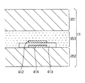
【0178】
ソース信号線414およびゲート信号線415は、液晶層353の比誘電率よりも低い誘電体膜413(以後、低誘電体膜と呼ぶ)で被覆されている。この低誘電体膜413によりストライプ状画素電極411とソース信号線414等が電磁的結合をひきおこすことを防止または制御している。低誘電体膜413としては、窒化シリコン(SiNX)、酸化シリコン(SiO2)、ポリイミド、ポリビニィールアルコール(PVA)、ゼラチン、アクリルが例示される。
【0179】
低誘電体膜413にはカーボン等の光吸収材が添加され、樹脂ブラックマトリックスとすることが好ましい。構成材料としては(図36)で説明した光吸収膜363と同じものを使用すればよい。ここでは説明を容易にするため、413は光吸収機能を有する樹脂ブラックマトリックス(以後、樹脂BMと呼ぶ)であるとして説明をする。
【0180】
一方、対向基板351にストライプ状の対向電極412(以後、ストライプ状対向電極と呼ぶ)およびカラーフィルタ356が形成されている。
【0181】
ストライプ状対向電極412はAl,Ti,Crの金属三層構成で形成される。ストライプ状対向電極412はブラックマトリックスとしても機能する。特に基板351と接する箇所は反射を防止するため6価クロム等で形成することが好ましい。その他対向基板351上に樹脂ブラックマトリックスからなるパターンを形成し、その上にITO等からなるストライプ状対向電極を形成してもよい。また、アクリル樹脂にカーボンなどを添加した有機導電体材料で形成してもよい。画素電極411も同様である。また、ストライプ状対向電極412の形成個所はソース信号線上あるいは近傍にのみ限定するものではなく、ゲート信号線上あるいは近傍に形成してもよい。
【0182】
なお、412はストライプ状対向電極としたが、ストライプ状に限定するものではなく、円弧状、円形状、三角錐状、円錐状、柱状など他の形状でもよい。つまり、画素電極411に対して対向電極として機能するものであればなんでもよい。画素電極411も同様である。
【0183】
液晶材料としてはΔnが大きいシアノビフェニール系を用いることが好ましい。また、ストライプ状画素電極411はITOで形成してもよい。ITOで形成すれば画素の開口率は向上する。
【0184】
(図41(b))で示すように、隣接したゲート信号線415上に絶縁膜(図示せず)を形成し、その上に電極418を形成することにより付加容量417(蓄積容量417)を形成している。また、電極418とストライプ状画素電極411とを接続している。なお、電極418はITOで形成してもよいし、Crなどの金属薄膜で形成してもよい。
【0185】
このようにストライプ状電極411と付加容量417とを接続することにより、ストライプ状画素電極411の電位を安定化する効果がある。そのためストライプ状画素電極411とストライプ状対向電極412間に発生する電気力線が安定して発生するようになる。
【0186】
(図42(a))は樹脂BM413がない場合の説明図である。ストライプ状画素電極411とストライプ状画素電極412間に電気力線417a、ストライプ状画素電極411とソース信号線414間に電気力線417bが発生する。液晶層353領域Bは、基板352に平行に電気力線417が発生しているため良好な光変調を行うことができる。液晶層353の領域Aの電気力線417a,417bは基板352に対して平行でない、ベクトル成分がある。したがって光変調に支障をきたし、ストライプ状対向電極412の周辺部から光漏れが発生する。
【0187】
(図42(b))は本発明の実施例の場合であり、かつソース信号線414上に樹脂BM413が形成されている場合である。なお、樹脂BM413は0.5μm以上2μm以下の膜厚に形成されている。樹脂BM413は比率電率が2以上10以下、さらに好ましくは2以上6以下の材料で形成されている。そのため、電気力線417bはほとんど発生しない。しかし、A領域で電気力線417aは発生する。そのため(図42(a))と同様に低いレベルではあるが、ストライプ状対向電極412の近傍で光ぬけが発生しようとする。本発明では413の低誘電体膜は光吸収膜材料で形成された樹脂BMであるのでA領域の光ぬけは遮光する。そのため光ぬけは発生せず、良好な光変調を行うことができる。
【0188】
本発明の実施例ではストライプ状画素電極411の近傍にも(図43)に示すように樹脂BM413bを形成している。ストライプ状画素電極411の近傍のA領域でも電気力線は基板352と平行でない成分が出現する。したし、樹脂BM413bを形成しているため、光ぬけの発生を防止することができる。
【0189】
なお、ストライプ状対向電極412、ストライプ状画素電極41のエッジから樹脂BMのエッジまでの距離をLとし、液晶層の膜厚をtとしたとき、以下の関係を満足させることが好ましい。
【0190】
【数10】
0.5≦L/t≦3.0
さらには、以下の関係を満足させることが好ましい。
【0191】
【数11】
1.0≦L/t≦2.0
L/tが小さすぎると光もれが発生しやすく、L/tが大きいと画素開口率を低下させ表示パネルの輝度を低下させる。
【0192】
なお、(図41)においてストライプ状対向電極412は対向基板351上に形成するとしたが、(図44)に示すように樹脂BM413上に直接形成してもよい。
【0193】
(図41)は1つのストライプ状画素電極411を有し、かつ、ストライプ状対向電極412を対向基板351上に形成した実施例であったが、(図45)に示すように、ストライプ状画素電極411を411a,411bと複数本形成し、ストライプ状対向電極412を412a,412b,412cというように複数本形成してもよい。ストライプ状対向電極412は絶縁膜451でソース信号線414と絶縁し、隣接画素と共通になるように形成されている。またストライプ状対向電極412とストライプ状画素電極411とは“く”の字状に形成している“く”の字状に形成することにより画素が青みがかかった色に、あるいは黄みがかかった色になる現象を抑制できる。“く”の字のθの角度はゲート信号線の垂直線を基準にして、5°≦θ≦30°とすることが好ましく、さらには10°≦θ≦20°とすることが好ましい。
【0194】
(図41)の表示パネルは、ストライプ状画素電極411で入射光を遮光する領域が発生するには画素開口率が低くなる欠点がある。(図46)の構成はこの欠点を対策する構成である。ただし、この構成は画素電極がストライプ状に限定されるものではない。
【0195】
マイクロレンズ基板362は、対向基板351に光結合層351で接着する。または、対向基板351内にマイクロレンズ361を配置または形成する。もしくはアレイ基板352に接着またはアレイ基板352内に形成または配置する。ここでは説明を容易にするために日本板硝子(株)が製造などしているイオン交換法で形成したマイクロレンズアレイ362を、対向基板351に接着した構成を例にあげて説明する。その他、(株)リコー、(株)オムロンが開発しているスタンパ技術で形成したマイクロレンズアレイを用いてもよい。また、レンズのカマボコレンズでもよく、フレネルレンズでもよく、回折効果により光を屈曲または進行方向を変化させるものでもよい。
【0196】
液晶層353がPD液晶(散乱型の光変調層)のとき、マイクロレンズ361の焦点距離t(μm)は、レンズの最大径をd(μm)としたとき、5d≦t≦20d以下となるようにする。されに好ましくは10d≦t≦18dとなるようにする。この範囲で最も表示輝度を高くでき、かつ、表示コントラスト向上効果が高い。
【0197】
本発明の表示パネルを投射型表示装置のライトバルブとして用いる場合は、以下の条件を満足させることが好ましい。投射レンズのFナンバーをFとし、このFからもとまる角度θ1(sinθ1=1/(2F))と、マイクロレンズのθ2(tanθ2=d/(2t))との関係は、θ1/3≦θ2≦θ1の関係を満足させるとよい。この範囲で高輝度表示と高コントラスト表示を両立できる。
【0198】
アレイ基板352には黒色塗料あるいはクロムなどの金属薄膜、誘電体ミラーで形成した膜あるいは遮光シート、板を配置する。もしくは(図36)の光吸収膜363と同様の光吸収膜461を形成する。ここでは説明を容易にするため、光吸収膜とする。また、マイクロレンズ361の焦点P位置に穴462(開口部)を形成または配置する。一例として、穴462はマイクロレンズ361の焦点に対応する位置に形成する。光吸収膜461は広義には遮光膜である。光吸収膜461はゼラチンなどからなるカラーフィルタを重ねて形成してもよい。また、光吸収膜461を形成した基板(図示せず)をアレイ基板352の表面などに配置または接着してもよい。また、光吸収膜461として偏光板、偏光シートなどを用いてもよい。また、回折格子などを形成してもよい。その他、アレイ基板352の光吸収膜を形成する箇所を研磨して白濁させたり、凹凸を形成してもよい。
【0199】
光吸収膜461の光吸収率は100%に近いことが好ましいことはいうまでもない。吸収率が50%以上で好ましい効果が大きく発揮される。また、吸収膜461を空気と接する面に形成または配置することにより冷却が容易となる。
【0200】
光吸収膜461は空冷の他、純水などで直接水冷してもよい。その他、1気圧以上好ましくは3気圧以上の水素で直接冷却することも効果がある。
【0201】
開口部462に点線で図示したようにカラーフィルタ356を形成または配置すれば1枚の表示パネルでカラー表示を実現できる。
【0202】
対向基板351およびアレイ基板352の厚みは、画素の開口率と焦点距離から決定する。(図46)のようにアレイ基板352と対向基板351の厚みが等しい(t1=t2)ときは、理想的にはマイクロレンズ361は、画素位置では画素サイズの1/4の領域を照明する。つまり、画素の開口率25%に対応することになる。画素開口率が1/4より大きい時は対向基板351の厚みを薄くする。逆の場合は光結合層122の厚みを厚くするなどして設計する。
【0203】
(図47)に示すように、マイクロレンズ361から液晶層353までの距離tとすると、焦点Pとの位置関係は以下のようにすることが好ましい。焦点P1は光吸収膜461の形成位置から+方向に距離tの位置であり、焦点P2は光吸収膜461から一方的に距離t離れた位置である。マイクロレンズ361の焦点位置PはこのP1からP2の範囲となるようにする。これは、画素開口率を関係があり、開口部462の面積を開口面積よりも小さくし、かつ、良好に画素開口部に光を入射できる範囲だからである。
【0204】
PD液晶層353が透明状態の時、入射光263は散乱されず、すべての入射光263は焦点Pに到達する。そのため、効率よく光が出射され、投射レンズの到達する。液晶層353が散乱状態のときは散乱した光は光吸収膜461で吸収または遮光される。そのため、アレイ基板352から出射されない。また、散乱光の出射割合は穴462径で決定される。穴462の面積が小さいほど穴462から出射する光が低下する。また、穴462から出射する光の割合は液晶層353に印加された電圧または散乱状態により変化する。
【0205】
(図46)の構成では、液晶層353が透過のときは効率よく穴462から出射し、散乱状態のときはほとんどの光は光吸収膜461で吸収される。したがって、PD液晶表示パネルの表示コントラストを大幅に向上できる。これは散乱モードの液晶に特有の効果であり、特に、投射型表示装置などのように表示パネルに入射する光の指向性が狭い装置に特有の現象である。理想的には穴462の面積を画素面積の1/2にすれば表示コントラストは2倍に、1/3にすれば3倍にすることができる。
【0206】
(図36)の表示パネルの構成において、反射電極354間から漏れる光を防止するためには、反射電極354間に樹脂ブラックマトリックスを形成すればよい。また、色純度を向上させるため、また隣接した画素で変調した光が画素に入射して不要な画像表示が発生することを防止するため、画素電極345上および対向電極355側にカラーフィルタ356を形成すればよい。たとえば対向電極355側にカラーフィルタ356R1が形成され、画素電極356R上にカラーフィルタ356R2が形成されているとする。液晶層353がPD液晶の場合、画素電極354Gで変調された光の一部は散乱光となり、画素電極354Rにも入射するが、この散乱光はカラーフィルタ356R1,356R2で吸収される。そのため、不要なハレーションが発生せず、画質が向上する。また反射電極354間には樹脂BM413が形成されているためアレイ基板352内へ光がほとんど侵入しない。さらに侵入した光は光吸収シート364で吸収される。したがってスイッチング素子(図示せず)に光が入射せずホトコンダクタ現象は全く発生しない。
(実施の形態7)
反射表示パネルの課題に、特に液晶層としてPD液晶を用いた反射型表示パネルの課題に反射電極で反射した光が直接、観察者の眼に入射し、表示画像の白黒が反転するということがある。
【0207】
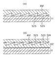
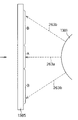
PD液晶表示パネルは液晶層353が白濁状態(散乱状態)の部分が白表示であり、光透過状態(透過状態:非散乱状態)が黒表示である。たとえば(図50(a))において、液晶層353が透明状態の場合、入射光263aは反射電極354で反射して対向基板351を出射する。この状態で観察者の眼が眼322aの位置であれば、NWモードの時、表示画像の表示は“白”、黒表示は“黒”と正しく表示される。しかし、観察者の眼が眼322bの位置であれば、眼322bに直接反射光263bが入射し、表示画像の白表示は“黒”、黒表示は“白”と反転して表示される(反転して見える)。この白黒反転現象をなくすためには、反射光263cのように極力反射光の角度θを大きくする必要がある。
【0208】
この課題に対応するため、本発明の表示パネルは(図50(b))に示すように表示パネル11の光入射面にノコギリ歯状の透過プリズム板(シート)491を配置している。プリズム板491はアレイ基板等の光入射側基板に光結合層122aで接着しても、また単に積載しても、あるいはアレイ基板上に直接樹脂等を用いて構成(形成しても)、アレイ基板等をプレス加工して構成(形成)してもよい。また、傾斜は(図51)に示すように背を向けるように配置する。
【0209】
傾斜の角度θ1は(図50(b))の基板352の垂直T0に対して以下の条件を満足するようにする。
【0210】
【数12】
40°≦θ1≦85°
好ましくは以下の条件を満足するようにする。
【0211】
【数13】
60°≦θ1≦80°
また、ピッチPは画素の対角長をdとするとき、以下の条件を満足させるようにする。
【0212】
【数14】
0.8≦P/d≦10
さらに好ましくは、以下の条件を満足させるようにする。
【0213】
【数15】
1.5≦P/d≦6
プリズム板491は、アクリル,ポリカーボネート,ポリエチレン,プロポリピレン樹脂を加工して形成することにより容易に形成できる。またガラス基板を切削あるいは、プレス加工することによっても形成することができる。
【0214】
(図49)に示すように、プリズム板491の表面には反射防止膜481を形成し、また、基板352の裏面に光吸収シート(膜)364を配置する。反射電極354の表面はAgで被覆している。また、反射電極354は誘電体ミラーとしてもよい。また、必要に応じて反射電極354の表面にマイクロオーダーの凹凸を形成してもよい。
【0215】
(図50(b))に示すようにθ2の角度で入射した入射光263aはプリズム板491によりθの角度の反射光263bとなる。つまり、θ2<θとなるため観察者の眼に反射光が直接入射することはほとんどなくなり、表示画像が白黒することはなくなる。
【0216】
プリズム板491において、画像表示に有効な入射光、出射光が通過しない領域には(図52(a))に示すように光吸収部521を形成する。光吸収部521は光吸収膜と363と同一材料を用いればよい。また光吸収部は遮光機能を有するものとしても実効的に用途として十分である。このように光吸収部521を形成(配置)することにより、プリズム板491内で不要なハレーションの発生を防止でき、表示コントラストの向上が望める。
【0217】
また(図52(b))に示すようにプリズム板491と透明のはりあわせ板522とをはりあわせる。もしくは一体として形成し、板状としてもよい。またはりあわせ板522をゲルもしくは樹脂を充填することにより代用してもよい。プリズム板491とはりあわせ板522との屈折率とは異ならせる。プリズム板491の屈折率n1は、はりあわせ板522の屈折率n2とはn1>n2とし、かつ、屈折率差Δn=n1−n2は以下の関係を満足させるようにする。
【0218】
【数16】
0.05≦Δn≦0.2
好ましくは、以下の関係を満足させるようにする。
【0219】
【数17】
0.1≦Δn≦0.15
また(図52(c))に図示したように、プリズム板491と平滑な平面板524間に樹脂,液体,ゲル等の充填材523を充填した構造でもよい。この場合も充填材523の屈折率をn2とし、前述の式に適合するようにすればよい。また、カラーフィルタ356は(図52(c))に示すように対向基板351もしくは、アレイ基板352間に配置もしくは形成してもよい。この場合は、液晶層353とプリズム板491間に位置する基板の厚みtは、画素サイズをdとしたとき(画素サイズが長方形の場合,d=(長辺+短辺)/2)、以下の関係を満足するようにする。
【0220】
【数18】
0.5≦t/d≦3
好ましくは、さらに以下の関係を満足するようにする。
【0221】
【数19】
0.8≦t/d≦2
また、プリズム板491はノコギリ歯状としたが、これに限定するものではなく、たとえば(図53(a))に示すように2つの斜面A,Cを有するノコギリ歯状でもよい。当然のことながらθ0の角度(DEG.)は小さい方が望ましいが、θ0(DEG.)は以下の条件を満足すれば実用上支障がない。
【0222】
【数20】
0°≦θ0≦45°
さらに好ましくは、以下の関係を満足するようにする。
【0223】
【数21】
0°≦θ0≦20°
また、Cの部分には光吸収部521を形成しておくことかが望ましい。
【0224】
その他、(図53(b))に示すようにA,B,Cの3つの面を有するものでもよい。またサインカーブ状,三角すい状,円すい状等を変形したものでもよい。また、ストライプ状あるいは、3次元状の凹凸状に形成したものでもよい。
【0225】
(図52)は斜面を表面にしたものであるが、これに限定するものではなく、(図54)に示すように斜面を表示パネル側に向け、平面を表面側としても同様の機能を実現できる。
【0226】
(図54)の変形例として、(図55(a))に示すように空間に充填材523を充填してもよいし、また(図52(c))と同様に(図55(b))に示すように、平面板524とプリズム板491との間にプリズム板491の屈折率よりも屈折率が大きい充填材523を充填してもよい。
【0227】
(図49)(図54)等の実施例は、表示パネルが反射型の場合である。表示パネル11が透過型の場合にも、プリズム板491を用いて表示画像が白黒反転することを防止できる。
【0228】
(図56)は画素電極356がITO等の透明電極で形成された場合である。プリズム板491の裏面には誘電体カラーフィルタ357が形成もしくは配置されている。表示パネル11に入射した光263aは、液晶層353を通過し、プリズム板491で屈折し誘電体カラーフィルタ357に入射する。この際入射角度が所定範囲にない場合、あるいは所定波長範囲内にない場合は誘電体カラーフィルタ357を透過する透過光263cとなる。誘電体カラーフィルタ357で反射した光はプリズム板491で屈曲し、反射光263bとなる。このようにして入射光263aは角度θの反射光263aに変換される。
【0229】
なお、プリズム板491の裏面に誘電体カラーフィルタ357を形成もしくは配置するとしたが、これに限定するものではなく、金属反射ミラーであってもよい。
【0230】
(図56)は表示装置を反射型として用いたものであったが、(図57)に示すように表示装置を透過型としてもよい。その実施例を(図57)に示す。(図57)では表示パネル11入射側にプリズム板491を光結合層491を介して取りつけている。そのため、入射光263aはプリズム板491により角度θの透過光263bとなり表示パネルを出射する。
【0231】
(図58)は透過型表示パネル11の出射面にプリズム板491を取り付けた構成である。プリズム板491の裏面にカラーフィルタ356を形成している。(図58)の構成でも入射光263aは角度θの出射光263bとなる。
【0232】
(図59)はプリズム板491を有する表示装置において、発光素子14と表示パネルとを一体として構成である。発光素子14は支持部591に取り付けられている。プリズム板491と表示パネルとが一体となるようにプリズム板491の周辺部をエポキシ樹脂等からなる封止樹脂で封止している。
【0233】
(図60)に示すように、発光素子14からの光263aは、プリズム板491のC面より入射し、A面での角度θ1は臨界角以上であるので、全反射して光263bとなり、反射電極354に入射する。反射光263cはプリズム491のA面で屈折してθ2の角度をなす出射光263cとなる。以上のようにして、発光素子14からの光は効率より表示パネル11の反射電極を照明する。
【0234】
以上の実施例はプリズム板491で入射光の方向を屈曲させるものであった。(図61)は反射電極354で入射光の方向を変化させるものである。(図61)は、断面図(説明図)である。
【0235】
反射電極354は、円弧状あるいは凹面状に形成されており、反射電極354はAl,Ag等の金属反射膜で形成される。また反射電極354の表面は図示していないが、反射電極354の変質等を防止するために、SiO2,SiNX等の無機材料で被覆されている。TFT等のスイッチング素子416はアクリル樹脂,ウレタン樹脂等の絶縁膜451で被覆され、絶縁膜451上に反射電極354aが形成されている。反射電極354aとTFT416のドレイン端子とは接続部611で接続されている。
【0236】
反射電極354aの形状(図62)に示すように円弧状にすることが好ましい。(図62(a))は1つの反射電極354aの平面図であり(図62(b))は(図62(a))のAA’線での断面図、(図62(c))は(図62(a))のBB’線での断面図。(図62(d))は(図62(a))のCC’線の断面図、(図62(e))は(図62(a))のDD’線での断面図である。
【0237】
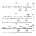
なお、(図62)では反射電極354aは円弧状としたが、(図63(a))のように凹面状としてもよい。また、(図63(b))のようにノコギリ歯状でもよい。また、(図63(b))は反射電極354上に透明樹脂631でノコギリ歯状の凸部を形成したものである。
【0238】
(図64)はノコギリ歯状等の凸部を有する反射電極354の製造方法の説明図である。まず、TFT等が形成されたアレイ基板352にアクリル樹脂あるいはSiO2等の膜641を形成する。この膜641上にレジスト塗布する(図64(a))。次にレジスト642を現象してパターニングする。パターニングは(図64(b))で示すように642aが最もほそく、642dが太くなるようにかつ、レジスト間の間隔が徐々に変化しているようにする(図64(b))。レジスト642間の間隔を変化させているため、エッチング箇所は(図64(c))に示すように644aが最も深くかつ広く、644dが最も浅くかつ狭くなる。次に(図64(d))に示すようにレジスト膜642を除去する。その後さらに膜641のエッチング液に浸せば、適度に角がエッチングされ(図64(e))のなめらかな傾斜を作製できる。その後、膜641上に反射膜643を蒸着することにより反射電極を形成することができる(図64(f))。なお、反射膜643は膜641との密着性を良好にするためTi,Cr,AgあるいはTi,Cr,Ag等の金属膜の複層構造とすることが好ましい。
【0239】
膜631は(図65(a))に示すようにノコギリ歯状、(図65(b))に示すように台形状でもよい。また、(図65(a))のように1つの反射電極354に対し、複数の凸部を形成しても、(図65(c))のように1つの反射電極354に対し、1つの凸部を形成してもよい。
【0240】
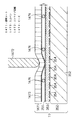
しかし、(図61)の構成では課題が発生する。それは(図61)のAの部分に電界が印加されにくく、PD液晶層が反射電極354に電圧が印加されても、白濁状態のままとなる点である。そのため、光反射率が低下する。
【0241】
この課題に対処するための構成が(図66)の構成である。反射膜643上にアクリル樹脂等の透明材料からなる平坦化膜631を形成し、前記平坦化膜631上にITOからなる透明画素電極345を形成したものである。透明画素電極345は複数の反射膜643に対して1つでもよく、また1つの反射膜の凸部に対し、1つの画素電極345を配置してもよい。
【0242】
(図66)のように形成することにより、(図61)のAで示したように電圧が印加されにくい部分がなくなり良好な光変調が行える。また、平坦化膜631を形成しているため画素電極354が平滑化され、液晶層353のギャップむらも発生しない。
【0243】
(図66)に示すように反射膜643の基板352の法線となす角度θ(DEG.)は以下の条件を満足することが好ましい。
【0244】
【数22】
60°≦θ≦85°
さらには、θ(DEG.)は以下の条件を満足することが好ましい。
【0245】
【数23】
70°≦θ≦85°
反射膜643と、画素電極354の配置状態は(図67)に図示する構成が考えられる。(図67(a))はスイッチング素子416としてのTFTのドレイン端子と画素電極354とが直接接続部611aで接続された構成である。反射膜643はどの電極とも接続されておらず、フローティング状態である。(図67(b))はTFTのドレイン端子と反射膜643とが接続部611aで接続され、さらに、反射膜643と画素電極354とが接続部611bで接続された構成である。ただし、反射膜643がAlの場合、ITOのAlとは電池反応するため、Cr,Tiあるいはカーボン等の導電体物質を介在させ電気的に接続する。(図63(c))は変形例であって、反射膜643上に直接ITO等の透明材料671を積層させ、かつ透明材料671で反射膜643を平滑化したものである。なお、この場合もITO671と反射膜643とが電池となることを防止するため、反射膜643と透明導電体(ITO)671間は絶縁膜等と分離しておく。
【0246】
なお、反射膜643は導電体材料からなる反射膜としたが、たとえば(図67(a)あるいは(図67(c))の場合等は反射膜643は導電性である必要ない。たとえば誘電体多層膜からなる誘電体ミラーとしてもよい。
【0247】
(図66)の構成は反射膜643上に画素電極354を形成することにより液晶層353全域に均一に電界が印加されるようにしたものである。他の実施例として、(図68)のように基板351と352の両方にノコギリ波状の電極を形成することによっても目的は達することができる。(図66)は対向基板351にカラーフィルタ356で凸部を形成したものである。この凸部上に対向電極355を形成している。当然のことながら、他の透明樹脂,無機材料等で凸部を形成し、この凸部上にカラーフィルタ356を形成してもよい。(図68)の実施例では反射膜を反射電極354としている。この(図66)の構成では液晶層353の膜厚は同一膜圧となるため液晶層に均一な電界が印加される。
【0248】
(図61)(図64)(図68)のように周期的な反射膜634凹凸の形成すると、回折現象が発生して光変調効率を低下させたり、回折像が発生して画像のにじみ等が発生することがある。この課題に対応するため、画素201R,201Gとの凸部の周期を変化させる。(図69(a))のAA’線での断面図を(図69(b))に示し、(図69(a))のBB’線の断面図を(図69(c))に示す。つまり、隣接した画素間で反射膜634のくりかえし同期が同相(周期が一致しない)とならないようにしている。このため、回折が発生しにくくなっている。またモアレ等も発生しにくい。
【0249】
(図69)の構成では凸部の周期が隣接した画素201間で90度位相をずらしているが、これに限定するものではなく、画素201R,201G,201Bで少しずつ(たとえば1/3周期ずつ等)ずらせてもよい。また、ランダムにずらせてもよい。また、(図69)では縦長方向に凸部を形成しているが、(図70ab)のように横方向に凸部を形成してもよい(図70のAA’断面参照)。この(図70)の構成では、入射光は両面の左右方向に反射する。
(実施の形態8)
以上のように(図61)(図64)(図68)の実施例では反射膜634により強制的に入射光の反射方向を変化させて、表示画像の白黒反転の現像を防止する構成であった。(図71)は所定角度の入射光のみを反射し、範囲外の入射光を透過させることにより表示画像の白黒反転現象を防止するものである。
【0250】
(図71)は本発明の表示パネルの断面図である。(図71)において樹脂からなる光吸収型のカラーフィルタ356が対向電極355に形成されている。一方、アレイ基板352には誘電体多層膜からなるカラーフィルタ357(誘電体カラーフィルタ)から形成されている。また誘電体カラーフィルタ357上にITO等の透明電極からなる画素電極354が形成されている。なお、以後、説明を容易にするためG光についてのみ説明する。しかし、他の色光についても同様である。
【0251】
(図72)に示すように入射光263aは樹脂カラーフィルタ356Gに入射し、G光以外の光は吸収されてG光の帯域の光のみが液晶層353および画素電極354にθ1の角度に入射する。今、説明を容易にするためθ1の角度で入射したとき誘電体カラーフィルタ357Gの分光反射率を(図73)の実線で示す。入射光の角度により分光分布が異なるのは、誘電体層に斜めに入射すると誘電体層中の光路長が長く、特性が長波長側にシフトするからである。逆に入射光が垂直に入射すると光路長が短くなり、特性が短波長側にシフトするからである。つまり誘電体カラーフィルタ357は入射光の角度により分光反射率分布が変化する。
【0252】
本発明は入射光263の入射角度により誘電体カラーフィルタの反射率(反射分布)が異なることを利用したものである。一方、樹脂カラーフィルタ354は入射光により分光分布がシフトするということはない(透過率が異なる)。本発明はこの性質を利用し、樹脂カラーフィルタ354で帯域制限をし、入射角が所定角度以内のときは誘電体カラーフィルタ357R,357G,357Bの特性は各入射する光の波長に応じて形成されている。
【0253】
入射光263cは画素電極354にθ2の角度で入射し、誘電体カラーフィルタ357Gの反射率は(図73)の実線であるから良好にG帯域の光は反射されて反射光263dとなる。入射光263aはθ1の角度で入射し、その時の誘電体カラーフィルタ357Gは点線で示されるから、G帯域の光のほとんどは透過してしまう。このようにして所定範囲で入射する光は透過してしまうため表示画像の白黒が反転するという現象は制御される。また誘電体カラーフィルタ357と樹脂カラーフィルタ354とで入射光の帯域制限をするため色純度が向上する。
【0254】
(図74)はマイクロレンズ361を用いて所定角度以内に入射する光は遮光し、表示画像の白黒反転を防止するものである。携帯型の表示装置(モバイル(携帯)機器)では、外光で画像を表示する。この外光は非常に平行性が良い場合が多い。たとえば、太陽光は虫メガネで集光できるように平行度が高い光線であり、また、室内光も天井の高い位置に蛍光灯が取りつけられているため平行度が高い。そのためレンズ等を用いて蛍光灯の像を結像させることができる。したがって、マイクロレンズ361は外光により焦点を結ばせることができる。
【0255】
(図74)においてマイクロレンズ361は外光を集光し、集光した光は反射電極354で反射して、遮光膜741で焦点を結ぶように構成されている。遮光膜741は(図36)の光吸収膜363と同様の材料からなる膜あるいは板、あるいはCr,Alなどの金属薄膜あるいは板もしくは光散乱性の物質等で構成される。
【0256】
(図75(a))に示すように表示パネル11に垂直に近い入射角度θ1で入射する光263aはマイクロレンズ361で集光され、その焦点は丁度、光吸収膜741に入射して吸収される。そのため表示パネル11から出射されることはない。一方、(図75(b))に示すように所定の角度θ2以上で入射する光263aは反射電極354で反射し、その焦点は光吸収膜741以外のところにある。そのため反射光263bは表示パネルから出射する。また、PD液晶層が散乱状態のときは、マイクロレンズ361で集光されることなくランダムに散乱される。そのため、一部は光吸収膜741で吸収されるがそのほとんどは表示パネルから出射し、観察者の眼に到達する。
【0257】
なお、(図75(b))で明らかなようにマイクロレンズの中心位置P1と画素の中心位置P2とは距離Lだけ偏差がある(図76参照)。この距離Lはマイクロレンズの形成位置から反射電極354までの距離tとの関係が、以下の範囲におさまるように定める必要がある。
【0258】
【数24】
2≦t/L≦30
さらに好ましくは以下の条件を満足する必要がある。
【0259】
【数25】
5≦t/L≦20
NWモードにおいて、PD液晶表示パネル等の散乱−透過状態の変化として光学像を形成する表示パネルの場合が、液晶355が透明状態の時、黒表示にする必要がある。この黒表示では反射電極354で正反射した光が観察者の眼に直接入射しないようにする必要がある。(図75)に示す実施例では、直接眼に入射する光は遮光膜741で遮光するから、表示画像の白黒反転現象は生じない。
【0260】
遮光膜741は反射光263b観察者の眼に直接入射しないようにするものであるから、すりガラスあるいはオパールガラス、あるいはTiを分散させた膜等の光散乱性を有するものでもよいことは言うまでもない。また、遮光膜741はマイクロレンズ361の光集光部を遮光するようにすればよいから、焦点位置に限定するものではなく、その近傍であればどこでもよい。また遮光膜741はマイクロレンズ基板362に形成せずともよい。たとえば別の基板に形成し、マイクロレンズ基板362あるいは対向基板351もしくは、アレイ基板352と接着等してもよい。また、遮光膜741は液晶層353が変調する光に対し、補色となる色素、染料を含むものでもよい。
【0261】
遮光膜741は(図77(a)に示すようにマイクロレンズ361の一部を帯状に遮光する形成(もしくは配置)してもよく、また、(図77(b))に示すようにマイクロレンズ361の光入射領域以外に遮光膜741を形成(もしくは配置)してもよい。また、(図77(c))に示すようにマイクロレンズ361の中心部を含む領域から遮光膜741を形成(もしくは配置)してもよく、(図77(d))に示すようにマイクロレンズ361の一部に形成(もしくは配置)してもよい。
【0262】
(図74)の構成はマイクロレンズ361は凸レンズの場合であったが、(図78)のように凹レンズ361aとしてもよい。この場合は、マイクロレンズ361aの周辺部に光吸収膜741で吸収される。また、入射光263aの角度が大きい場合は光吸収膜741で吸収されず表示パネル11から出射される。
【0263】
その他、(図79)のように反射電極354上にITO等の透明導電性材料からなる凸レンズまたは凹レンズ361bを形成し、対向基板351の表面等に光吸収膜741を形成する構成でもよい。なお、ITO等でレンズ361bを形成する場合は、該レンズ361bと反射電極354のAl膜とは絶縁材料451で絶縁しておくことが好ましい。
【0264】
また、入射光263を拡散させる目的であれば、(図80)に示すように反射電極354上にITOからなる2次元もしくは3次元状の回折格子801aを形成してもよい(図80(a))。もしくは、対向電極355上に回折格子801bを形成してもよい。(図80)に示す実施の形態の特性は、ITO等の透明でかつ導電性材料で回折格子801を形成することにより、液晶層353に均一に電界が印加されるようにし、かつ、回折格子801で入射光もしくは反射光が遮光されることがなく、かつ良好に光拡散するようにしたことである。回折格子801の材料、構成については(図167)と同様にすればよい。
【0265】
なお、以上の本発明の表示パネル、表示装置の実施例において主として対向基板351にカラーフィルタ356,357を形成するとしたが、これに限定するものではなく、(図82)に示すように誘電体カラーフィルタ357もしくは、樹脂カラーフィルタ356上にITOからなる画素電極354を形成してもよいことは言うまでもない。また、(図82)に示すように透明電極821となるITOとSiO2等の誘電体薄膜とを積層して反射電極を構成するとともに、画素電極もしくは対向電極としてもよい。
【0266】
(図66)などは画素電極の下層に反射膜643が配置または形成された構成であるが、反射膜643部は(図167)に示すように回折格子801としてもよい。
【0267】
(図167)は本発明の液晶表示パネルの断面図である。ただし、図面はモデル的に描いている。アレイ基板352上回折格子801が形成され、前記回折格子801上に反射膜643が形成されている。図167では回折格子801は矩形状に図示したがこれに限定するものではなく、三角形状、サインカーブ状、台形状のいずれであってもよい。また、一次元回折格子だけでなく、2次元回折格子でも良い。回折格子のピッチの一例として0.5μm以上20μm以下の範囲が好ましい。さらには1.5以上10μm以下の範囲が好ましい。また、高さは0.5μm以上8μm以下の範囲が好ましく、さらには1μm以上5μm以下の範囲が好ましい。
【0268】
また、画素電極354は(図167(b))で示すように微小な凹または凸もしくは凹凸1672を形成しておくとよい。凹凸の高さは0.5μm以上2μm以下とする。さらに好ましくは、0.8μm以上1.5μm以下とする。このように微細な凹凸1672を形成することのより、入射した光の方向が適度に屈折され視野角が広くなる。なお、微小凹凸354は(図167)の反射膜643に形成してよい。また、(図66)などの表示パネルの反射膜643に形成してもよいし、(図54)などの反射電極354に形成してもよい。また、微小凹凸1672を微小な拡散点とすることにより更に視野角などの改善効果が得られる。
【0269】
回折格子の材料としてはSiOx、SiNx、TaOx、ガラス系物質などの無機物質、レジストとして用いられる材料、ポリイミド、アクリル系樹脂などの有機物質などが例示される。材料の選定としては透明膜631の屈折率に対応して決める。透明膜631の屈折率は1.45〜1.55、回折格子の屈折率は1.45〜1.55のものがよく用いられる。
【0270】
回折格子801の形成材料としては、現状の無機材料としては、プロセス上形成・加工が容易なSiO2が適している。SiO2の屈折率は通常1.45〜1.50程度である。また、形成方法としてはSiO2を蒸着後、パターンマスクを形成しエッチングすればよい。あるいはガラス基板352あるいは351をフォトリソグラフティとドライエッチングの手法を用い直接に回折格子801を形成しても良い。また、有機材料としては液晶層353に用いるものと同一の透明なポリマーを用いるのが最適である。また、通常の半導体の製造に用いるレジスト材料なども用いることができる。上記のような材料を用いた回折格子801の形成方法としては、ロールクォーターあるいはスピンナー等で基板上に塗布し、パターンマスクを用いて必要な部分のみ重合するなどすればよい。また、ポリマー+ドーパントからからなる感光性樹脂を基板にスピンコートし、パターンマスクを介して露光したのち、減圧加熱によりドーパントを昇華させる方式でドライ現像する方法もある。
【0271】
回折格子801のピッチ、高さは変調する光の波長、液晶層353の屈折率及び光学系の光の指向性および必要とする回折効率などによりかなり異なる。従って、ピッチp・高さは光学系の光の指向性、回折角度、波長により決定すべきである。しかし回折格子801形成上のプロセス条件などに左右されることも多い。およそピッチは1μm〜15μmであり、中でも1μm〜10μmが最適である。これは本発明の液晶表示パネルを液晶投写型テレビに用いる際の投写レンズのF値を考慮して定めるべきである。およそF値が5.0のときピッチは5μm以下、7.0のときピッチは8μm以下に設定する。なお、プロセス上、回折格子801の形状はサインカーブ状あるいは台形状となることが多い。
【0272】
高さは、回折効率に大きく依存する。高さは0次光を0にしようとすると1〜4μm必要である。しかし、通常、0次光を完全に0にする必要はなく、回折効率が40〜70%でよいから高さは2〜3μmでよい。
【0273】
なお、回折格子801は透過型であってもよい。また、回折格子801の下層あるいは基板352が空気と接する面に反射膜を形成または配置してもよい。これらの回折格子801に関する事項/内容は(図80)の本発明の表示パネルあるいは表示装置についても同様である。
【0274】
光変調層353はTN液晶、PD液晶あるいはPLZTなどのいずれの種類光変調材料で形成してよいが、ここでは説明を容易にするため光変調層353はPD液晶であるとして(図168)を用いて説明する。(図168(a))は、PD液晶層353に電圧が印加され、透明状態である場合である。この場合は液晶層353に入射した光263aは液晶層353、画素電極354を透過し、回折格子801で回折される。したがって、(図50)で説明したような、反射光が直接に観察者の眼322bに入射することはない。
【0275】
(図168(a))はPD液晶層353が散乱状態の場合である。散乱状態の場合は入射した光263bは液晶層353で散乱され、散乱光263bとなる。したがって、入射光263aは回折されることはない。散乱光263bはノーマリホワイトモードの場合、観察者は白表示として認識する。
【0276】
以上のように、画素電極353の下層に回折格子801を形成することにより、反射光が直接に観察者の眼に到達する割合は大幅に減少する。そのため、視野角の広い高コントラクト表示を実現できる。
(実施の形態9)
以上の実施例は、外光で画像表示を行う構成について説明をした。しかし、全く外光がない場合は発光体、発光素子をもちいて表示パネルを照明する必要がある。
【0277】
(図83)はバックライト12により液晶層353を照明する構成である。(図83)の特徴は反射型の表示パネルにおいて、反射電極354のすきまからバックライト12の光を液晶層353に入射させ照明することである。
【0278】
バックライト12の表面にはストライプ状に反射膜343が形成されている。反射膜343間には開口部462があり、この開口部462を焦点位置とするマイクロレンズ361が配置されている。マイクロレンズ361はカマボコレンズ状(ストライプ状)である。なお、マイクロレンズ361がドット状の場合は、当然のことながら反射膜343はドット状の開口部462を有する構成にする。この開口部462をドット状のマイクロレンズ361の焦点位置とする。
【0279】
マイクロレンズアレイ362は反射電極354が形成された基板352に接着されている。またマイクロレンズ362の焦点位置は反射電極354間の光入射部832より入射する。このように画像表示に無効な領域(反射電極間)からバックライト12の光を入射させることにより画素開口率は低下せず、かつ良好に反射電極354を照明できるようになる。
【0280】
光入射部832から入射した光は反射ブラックマトリックス(反射BM)831で反射され反射電極354を照明する。反射BM831はAg,Al等の反射率の高い金属薄膜で形成することが好ましい。反射BM831は反射電極354を照明するとともに、(図83)のA方向から見たとき、反射電極354間から光ぬけが発生することを防止する機能を有する。
【0281】
このように光入射部832から光を入射させることにより、外光が全くない場合でも反射電極を照明することができ、またバックライト12の光利用効率も高くできる。なお、反射BM831は光拡散材などの光を拡散させる材料で構成してもよい。あるいは誘電体ミラーで構成してもよい。
【0282】
(図83)に示す実施の形態の作用は、(図84(a))に示すように、反射膜343間の開口部462から入射光263aが入射し、レンズ361で集光263bされて反射BM831で反射されて、反射光263cとなり反射電極354を照明するものであった。しかし、(図84(b))に示すようにマイクロレンズ361がなくとも、バックライト12からの光263bを集光することなく、光吸収部832から入射させ、反射BM831で反射させて反射光263cとしてもよい。(図84(b))の構成はバックライトの光利用効率は低下する方向にあるが、マイクロレンズアレイ362が不要で低コスト化を実現できる。
【0283】
マイクロレンズ361aはカマボコ型のものを用いるとしたが、配置は(図85)に示すように光入射部832下に形成(配置)すればよい。また、(図85(b))に示すようにカマボコ型のマイクロレンズ361a,362bを交差させて配置してもよい。
【0284】
また、反射BM831(図86)に示すようにくさび状もしくは、三角すい状等の凸部631上に形成してもよい。入射光263aは反射BM831で反射され反射光263bとなり反射電極354aを効率よく照明する。また、(図87)に示すように反射BM831上に凸レンズもしくは凹レンズ831を形成し、入射光を屈曲させて反射電極354を照明してもよい。また、(図88)に示すように画素電極354上にカラーフィルタ356を形成し、かつ、反射BM831上に平坦化膜451を形成してその上に対向電極を形成してもよい。このように反射BM831と対向電極355とを平坦化膜451で絶縁するのは、対向電極355のITOと反射BM831のAl薄膜とが接触して電池となるのを防止するとともに、反射BM831の形成による凹凸を軽減するためである。
【0285】
その他の構成として、(図89)のように反射電極354間832に光拡散層もしくは光拡散膜891を形成もしくは配置してもよい。光拡散層891に入射した光263は散乱することにより反射電極354を照明する。もちろんあわせて反射BM831を形成してもよい。
【0286】
光拡散層891は、PD液晶を常散乱状態とすることにより、あるいはアクリル樹脂等に酸化Ti等の金属微粒子を分散させることにより、あるいは異種の屈折率材料を混合させることにより形成する。
【0287】
なお、これまでの実施例において液晶層353はPD液晶層とすることが好ましいが、散乱性の光変調層として動的散乱モード(DSM)、強誘電液晶を厚く形成したもの、PLZTなどがある。その他STN,TN液晶などでもよい。
【0288】
(図83)等の実施例では(図90(a)に示すように反射電極354間からバックライトの光を入射させるとしたが、これに限定するものではなく、(図90(b))に示すように反射電極354の中央部等に透明電極等により光入射部832を形成し、この光入射部832から光を入射させてもよい。また、(図90(c))に示すように中央部に円状の透明部を形成し、この部分から入射光を入射してもよい。
【0289】
(図61)(図66)などの反射型表示パネルは、図の点線で示すように、裏面にバックライト(光発生手段/照明装置)15(12)を配置することにより、バックライトからの光で画像を表示させることができる。この構成の場合は光吸収シート364は取り除く。バックライト15から放射された光263aは反射膜643の裏面で反射し反射光263bとなり、反射膜と反射膜との隙間より出射し、今度は反射膜643の表面で反射して反射光263cとなる。反射膜643の両面は良好な反射面に形成されているからである。反射光263cは、液晶層353が透明状態の時はそのまま対向基板351から出射し、黒表示となる。液晶層353が散乱状態の時は散乱し、白表示となる。
【0290】
この構成では、それぞれ隣り合った反射膜643の隙間を利用して液晶層353に光を入射させるために開口率を低下させることもなく、また、フロントライト方式を用いる必要がなくなる。なお、バックライトはキセノンランプなどを用いる照明光学系を採用してもよい。したがって、投射型表示装置、ビューファインダにも用いることができる。また、(図66)に示す反射型画素の隙間を用いて照明する方式は(図66)(図68)(図71)(図102)の構成に用いてもよい。
【0291】
なお、反射膜643は完全に反射ではなく、半透過状態でもよい。例えば、反射膜643の反射率が70%で透過率を30%とする構成が例示される。
【0292】
たとえば、(図90(c))の構成の断面図は(図91(a))のようになる。透明電極821上に反射電極343が形成されている。光入射部832上に反射BM832が形成されている。(図91(b))は(図90(a))の構成に加えて対向電極355にカラーフィルタ356が形成された実施例である。
【0293】
また、(図83)等の実施例ではバックライト12からの光で照射するとしたが、バックライトとは光発生物と考えるべきである。一般的な面発光バックライトの他電球や、LEDバックライトまたは外光をミラーでおりまげて導入したもの等も含まれる。
【0294】
(図92(a))のようにR画素が354R,354G,354Bのストライプ状の場合も光入射部832から光を入射させればよいし、(図92(b))のように反射電極354の中央部に透明部を形成して光入射部832を形成してもよい。また(図92(c))のように縦方向に光入射部832aを形成し、かつ横方向に光入射部832bを形成してもよい。
【0295】
なお、(図93)のように反射電極343上に凸部631を形成し、かつ凸部631上に透明電極821を形成することにより、光変調効率を向上させることができる。
【0296】
反射電極363は、(図94)に示すように透明画素電極821上に絶縁膜451を形成し、その絶縁膜451上に形成してもよい。(図94)に示す構成の等価回路は(図95)のようになる。反射電極363が形成された部分は、誘電体層として451と液晶層353の2つが形成され、2つのコンデンサ951a,951bが形成される。一方透明電極821上に液晶層353のみであるから1つのコンデンサ951cが形成される。したがって、反射電極363が形成された部分は誘電体451と液晶層353で印加電圧が分圧される。分圧された箇所の液晶層353には電圧が印加されにくくなる。
【0297】
この状態を図示すると(図96)のようになる。図中の液晶層353において、透明電極821上のCの部分は最も強く電圧が印加される。反射電極363上のAの部分は、前記Cの部分よりも弱い電圧が印加される。Bの部分はCとAの中間程度の電圧が印加される。したがって、CとAの部分では液晶配向状態が異なるようになるから、視野角の拡大が実現できる。
【0298】
また、反射電極363と透明電極821とはそれぞれ異なるスイッチング素子に接続してもよい。なお、以下の実施例において反射電極363と透明電極821として説明するが、これに限定するものではなく、2つの電極とも反射電極あるいは透明電極であってもよい。
【0299】
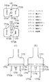
(図97)に示すように透明電極821はTFT416aに接続され、TFT416aのドレイン端子には、TFT416aのソース端子と接続されている。TFT416bのドレイン端子には反射電極363が接続されている。TFT416aはTFT416bよりもW/L(チャンネル幅/チャンネル長)が大きい。そのためTFT416aのオフリーク量はTFT416bよりも大きい。またTFT416bはTFT416aのドレイン端子に接続されているため(直列接続)TFT416bはオフリーク量が少ない。したがって、反射電極363上の液晶層353は1フィールドの間十分な電圧が印加される。透明電極821上の液晶層821はTFT416aがリークするため1フィールド間に印加される実効電圧が小さくなる。そのため、実効電圧が異なる2つの液晶層が生じるため視野角が大きくすることができる。もちろんのことながら、TFT416aのW/LをTFT416bのW/Lよりも小さくしてもよい。本方式は、複数のTFT416のリーク電流の量を異ならせることにより、2つの画素電極に印加される実効電圧を変化させるものであればよいからである。
【0300】
(図97(a))は2つのTFT416a,416bのゲート端子を同一ゲート信号線415に接続したものであるが、(図97(b))のように異なるゲート端子に接続してもよい。また(図97(c))のようにTFT416bを形成せず、コンデンサ951によって電極363に電圧を印加できるように構成してもよい。
【0301】
(図97(a)(b))はTFTを直列接続した構成であるが、(図98(a))に示すようにTFT416を並列にしてそれぞれ別の電極(821,363)に接続してもよい。また(図98(b))のように接続してもよい。
【0302】
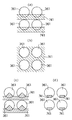
なお、透明電極821と反射電極363とは(図99(a))に示すようにくし型に組み合わせてもよいし、また(図99(b))のように同心円状に組み合わせてもよい。反射電極363と透明電極821とは重ねて形成する必要はなく、(図100(a)(b))のように反射電極363と透明電極821が重さならないように形成してもよいし、また、1つの画素に反射電極363、あるいは透明電極821を複数形成してもよい。
【0303】
なお、以上の実施例では反射電極363、透明電極821としたが、これに限定するものではなく、両方が反射電極、両方が透明電極とおきかえてもよい。
【0304】
(図101)の実施例は対向基板351およびアレイ基板352の両方に反射電極(反射膜)を形成し、A方向からもB方向からも表示画像を見えるようにした構成である。
【0305】
対向基板351の対向電極355上に絶縁膜451を形成し、その上にAlからなる反射膜363bを形成している。また、アレイ基板352には透明画素電極821上に絶縁膜451を形成しその上に反射膜363aを形成している。B方向から見たとき反射膜363bが見えるようにA方向からみたとき反射膜363aが見えるようにしている。そのため、反射型の表示パネルでありながら、A方向からもB方向からも表示画像が見える。反射膜363はドット状、あるいはストライプ状に形成される。
【0306】
(図102)は(図101)に加えて三角状あるいは円弧状の凸部631上に反射膜363を形成したものである。このように形成すれば入射光の角度が曲げられ、より良好に表示画像を見られる範囲が広がる。また、(図103(a))は(図102)の凸部631の角度を変化させたものである。
【0307】
(図103(b))はマイクロレンズ361の焦点位置に反射膜363を配置した実施例である。マイクロレンズ361aは入射光263aを集光する。集光した光は反射膜363aで反射する。マイクロレンズ361bは入射光263bを集光し、集光した光は反射膜363bで反射する。このように構成することにより入射光はすべて反射膜363では反射されるようになるから、開口率が向上する。
【0308】
(図83)(図86)(図94)(図101)(図103)などで説明した透過型あるいは反射と透過の両方のモードで画像を表示する表示装置/表示パネルには(図124)の光路制御板1242あるいは(図26)の反射鏡261の原理あるいは方式を応用してバックライト部(パネルの照明部)を構成することにより良好な指向性の画像表示を行うことができる。この説明図を(図176)に示す。(図176)のように光の方向を制御するのは(図48)などで説明したように観察者の眼に直接入射する光を抑制するためである。この現象は特にPD液晶の場合に問題になることが多い。
【0309】
(図176)はバックライト15の光出射側に光路制御板1242を配置した指向制御部1243の構成例である。光路制御板1242またはミラー261は透明樹脂内に埋め込まれている。これらの制御板などは画素行方向に配置されている。つまり、画面の上下に指向性があるように構成されている。光路制御板1242は樹脂内に封止されている例を例示しているが、これに限定するものではなく空洞中に配置されていてもよい。指向制御部1243は表示パネル11と光結合剤122でオプティカルカップリングされている。
【0310】
光路制御板1242は1mm以上10mm以下の間隔で配置される。制御板1242はバックライト15などからの光を(図176)に示す光路263のように斜め方向の光を出射する。そのため、表示パネル11の液晶層353が光透過状態の時は、光263は光変調層を通過し表示パネルを出射する。したがって、観察者の眼に直接入射することはない。光変調層353が散乱状態の時は光263は散乱し、白表示となる。
【0311】
指向制御部1243の代わりに(図177)に示すようにプリズム板491を表示パネル11の裏面に配置してもよい。プリズム板491はバックライト15とオプティカルカップリングさせる。プリズム板491を用いても表示パネル11に入射する光は斜め方向(図177の光路263参照)に入射させることができる。
(実施の形態10)
以上に説明した表示パネルは本発明の表示装置等にすべて用いることができる。以下図面を参照しながら本発明の表示装置について順次説明をする。
【0312】
(図104)は本発明の映像装置としての液晶モニタ(液晶テレビ)の説明図である。本発明の液晶モニタは2つの表示領域をつなぎあわせて、1つの、あるいは疑似的に1つの表示領域として用いることを目的としたものである。
【0313】
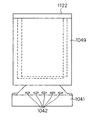
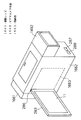
(図104(a))は液晶モニタを正面から見た図であり、(図104(b))は側面から見た図である。(図104(a))に示すように、表示パネル11は右側に寄せて取りつけられたような構成となっている。つまり左側にはパネルカバー1049があるが、右側は好ましくはその端部まで画像表示領域61である。もちろんパネル11の端部を保膜する緩衝材を配置してもよい。
【0314】
表示パネルが取り付けられたパネルカバー1049は、保持台1041に取り付け部1043を介して、取りつけネジ1044で取り付けられている。保持台1041には、電源オンオフスイッチ,クロックの位相スイッチ等の制御ボタン1042が取り付けられている。また、パネルカバー1049は取り付けネジ1044で容易に取りはずすことができ、取りはずした表示パネル11は、その上下の向きを逆にして保持台1041に取り付けることができる。また、逆むきに取り付けたとき、画面の走査方向は自動的に逆向きとするため、判別スイッチが別途設けられている。また、必要に応じて逆走査スイッチを制御スイッチ1042として配置しておく。また、取りつけネジ1044を用いず、保持台1041とパネルカバー1049をはめこみ式としてもよい。つまり容易に取りはずしができる構造のものであれば何でもよい。
【0315】
パネルカバー1049を上下逆転させて取りつけることが容易なように、パネルカバー1049からLVDSなどのパネルリンクコネクタ1045、バックライトなどに電源を供給するバックライトコネクタ1046が付加されており、これらのコネクタを保持台1041に差しこめるようになっている。なお、パネルリンクコネクタ1045はLVDS方式の差動信号が伝送されるコネクタであり、このコネクタを介してデジタル化された映像信号が表示パネル11に供給される。またバックライトコネクタ1116は、バックライトを構成する蛍光管および表示パネル11に電源を供給するコネクタである。
【0316】
保持台1041には、電源コネクタ1048とアナログ映像信号を入力するVGAコネクタ1047が配置されている。保持台1041内にアナログ映像信号をA/D変換してデジタル信号とする回路および映像信号および定電圧電源回路が配置されている。
【0317】
表示パネル11は、(図105)に示すようにパネルカバー1049a内に配置されている。(図105)は、説明を容易にするために、本発明の液晶モニタを2台並列に並べたところを示している。表示パネル11は表示領域の中央部Pがパネルカバー1049の中央に位置するように配置されている。したがって、図示するように、それぞれ正方向と逆方向とに取り付けた2つの表示パネル11を並列に並べた時、2つの表示領域61aおよび61bの画面中心P1とP2とを結ぶ直線が、該表示領域61aおよび61bの長手方向と平行になるように構成されている。
【0318】
表示パネル11には、左右の一片部のみにゲートドライバ1051が低温ポリシリコン技術で形成されているか、もしくはシリコンチップとしてCOG(チップオンガラス)技術で接続されている。また、上下の一片部のみにソースドライバ1052が低温ポリシリコン技術で形成されているか、もしくはシリコンチップとしてCOG技術で接続されている。したがってBで示すエッジ部は、そのぎりぎりまで画像を表示する表示領域に含まれる。
【0319】
パネルカバー1049bを逆に取り付けてパネルカバー1049aの横に配置すれば、(図110)に示すように表示領域61aと61bとから構成される1つの大きな横長の表示モニタとなる。たとえば表示パネルが4:3の1024×768ドットのXGA表示パネルであれば、1024×(768+768)ドットの8:3の表示パネルを得ることができる。
【0320】
パネルカバー1049aの走査方向が、図中XYで示す実線の走査方向であれば、逆取り付けしたパネルカバー1049bの走査方向は点線で示すように、逆走査にする必要がある。しかし、これは容易であってゲートドライバ1051およびソースドライバ1052のシフトレジスタの走査方向を逆にすればよい。そのため、パネルカバー1049に取り付け方向を自動的に検出するための自転検出スイッチを設けることあるいは逆走査スイッチを制御スイッチを制御ボタン1042として配置すればよい。
【0321】
(図110)に示すように、表示パネル11aはパーソナルコンピュータ1102内に配置されたグラフィックボード1101aから映像信号の供給を受け、表示パネル11bはグラフィックボード1101bから映像信号の供給をうける。グラフィックボード1101aがメインボードであり、グラフィックボード1101bがスレーブボード(従属ボード)として動作する。このメインとスレーブボードの制御は、例えばウインドウズ98のようなオペレーティングシステムによって制御される。そしてあたかも3:4の縦横比を有する二つの表示領域を、3:8の縦横比を有する、一つの横長の表示領域のように取り合うことができる。
【0322】
本発明の液晶モニタの効果は、パネルカバー1049の端部に表示領域を配置し、かつ、上下逆転させて取り付けることができるように構成したことにより、1種類の同一液晶モニタを製造しているにもかかわらず、ユーザが表示パネルを買い増すことにより容易に3:8の表示ディスプレイに変更できる点にある。また(図111)に示すようにユーザが表示領域61を見やすいように表示領域61aと61bとを角度をつけて配置できることである。
【0323】
(図112(a)(b))は本発明の他の実施例における液晶モニタの構成を示す図である。(図112(b))は平面図であり、(図112(a))は断面図である。2つの表示パネル11aと11bは1つの保持台1041に取り付けられており、パネルカバー1049aと1049bとはおりたためるように構成されている。パネルカバー1049aと1049bとは容易に平面状となるように支持部1122が設けられており、また、表示パネル11aと11bとがおりたたんだときに接触しないように、パネルカバー1049の一部に緩衝部材1121が取り付けられている。緩衝部材とはスポンジ,バネ,ゴム等が例示される。
【0324】
パネルカバー1049の裏面は、(図114)に示すように、保持台1041の取り付け部1043を填め込むための取り付け溝1141が設けられている。この溝1141と取り付け部1142によりパネルカバー1049は回転できるように構成されており、(図113)に示すように、表示部は使用時に際して90度回転し、かつ非使用時には折り畳んで収納できるように構成されている。
【0325】
(図112)等は2つの表示パネル11を用いて1つの表示領域61を構成する構成であった。(図115)は1つの表示パネル11に2つの表示領域61a,61bを形成した構成である。
【0326】
ゲートドライバ1051a,1051bが接続されたゲート信号線Gj(jは正の整数)は2つの表示領域61a,61bに共通である。また2つの表示領域61aと61b間に輝度分布が発生することを防止するため、ゲートドライバ1051aは奇数番目のゲート信号線を駆動し、ゲートドライバ1051bは偶数番目のゲート信号線を駆動する。これはゲート信号線の信号供給例と供給されない側間の電位差による表示の差異をめだたないようにするためである。一方、ソースドライバ1052aはグラフィックボード1101aから処理された映像信号を映像入力端子1151aより供給され、表示領域61aに第1の画像を表示する。同様にソースドライバ1052bはグラフィックボード1101bから処理された映像信号を映像入力端子1151bより供給され表示領域61bに第2の画像を表示する。この表示状態を(図116)に示す。
【0327】
(図116)の実施例では表示領域61aと61bの継ぎ目は発生しない。また、表示領域61aと61bではゲートドライブ1051が共通であるので、ゲートドライブの使用個数を低減でき低コスト化が望める。これらの構成、方法はNTSC、HDの動画を表示するテレビにも採用できることは言うまでもない。
【0328】
本発明の表示装置にNTSCあるいは1080iなどのインタレース信号を表示するため以下に説明する表示方法を採用している。(図106)(図107)は本発明の表示方法の説明図である。まず、(図107)に示す静止を表示する方法について説明をする。
【0329】
(図106(a))は入力されたインタレース信号の第1フレームを表示パネル11上にそのまま表示したときの画像61を示し、(図106(b))は入力されたインタレース信号の第2フレームを表示パネル11上にそのまま表示した画像61を示している。なお、第1および第2のフレームは、時間的に連続したフレームである。また、第1のフレームは奇数ラインを第2のクレームは偶数ラインを有するフレームである。
【0330】
まず、入力されたインタレース信号の第1フレームの第1ラインを表示パネル11上の第1ラインに表示する(1−1で示す)。次に、第1フレームの第3ラインを表示パネル11上の第3ラインに表示する(1−3で示す)。
【0331】
以下、第5ライン(1−5),第7ライン(1−7)…というように、第1フレームの映像信号を順次表示パネル上の奇数ラインに表示する。(図107(a))。
【0332】
一方、第2フレームの第2ラインを表示パネル11上の第2インチに表示する(2−1で示す)。次に第2フレームの第4ラインを表示する(2−4)。以下、順次繰り返すことにより(図107(b))の状態となる。したがって第1のフレームと第2のフレームで奇数ラインと偶数ラインが表示され1つの表示領域が完成する。以上の操作を第3フレーム(奇数)、第4フレーム(偶数)にも同様に施し、以後繰り返す。以上の表示モードを静止モード表示と呼ぶ。
【0333】
上記のように、入力されたインタレース信号の2フレーム期間で、第1のフレームの奇数ラインと第2のフレームの偶数ラインとからなる1フレームを表示すれば良いため、映像信号処理回路が簡略化され、かつ、高精細の表示画像を表示できる。
【0334】
次に、第2の表示方法について説明する。(図106(a))は入力されたインタレース信号の第1フレームを表示パネル11上に表示したときの画像状態を示し、(図106(b))は入力されたインタレース信号の第2フレームを表示パネル11上に表示した画像状態を示している。まず、入力されたインタレース信号の第1フレームの第1ラインを表示パネル11上の第1および第2のラインに同時に同じ表示をする。次に、第1フレームの第3ラインを表示パネル11上の第3および第4のラインに同時に表示する。以後、第5,第7ライン…というように、第1フレームのラインを順次表示パネル11上の奇数ラインと隣接偶数ラインに同時に表示する。その結果、(図106(b))に示す画像が得られる。一方、第2フレームにおいては、偶数ラインだけを表示パネル11上の偶数ラインと隣接奇数ラインに同時に表示する。ただし、表示パネル11の第1ラインには表示しない。つまり、第1のフレームと1ラインずれて画像を表示する。その結果、(図106(b))に示す画像が得られる。以上の操作を第3フレーム,第4フレームにも同様に施し、以後繰り返す。以上の表示モードを動画モード表示と呼ぶ。動画モード表示では、表示パネル11の第1ラインは1−1のみ、第2ラインは1−1と2−2が平均された表示、第3ラインは1−3と2−2が平均された表示となる。
【0335】
以上2つの表示方法について示したが、静止画の場合は(図107)の静止モード表示を選択し、動画の場合は(図106)の動画モード表示を選択するのが好ましい。静止画は画像が停止しているため、動画に比べて垂直方向の画像の不連続性が視認されやすい。そのため、静止画の場合は、動画モード表示でフレーム間での内挿(フレーム補間)を行うことにより、見かけ上の垂直解像度を確保することが好ましい。一方、動画は時間的な画像の変化が激しいため、動画モード表示を適用すると、いわゆる動画ボケ(ジャーキネス妨害等)が発生する。そのため、動画の場合は、動画モード表示でフレーム内での内挿(ライン補間)を行うことにより、動画ボケの発生を防止することが好ましい。
【0336】
通常、NTSC等のインタレース信号の表示画像を見る場合は動画モード表示で使用する。写真あるいは文字資料,文献等が連続して表示される場合(表示される場合)は静止モード表示に切りかえて使用する。
【0337】
静止モードと動画モードとの切り換えは表示装置に取り付けられた制御スイッチあるいは(図109)に示すリモートコントローラ(以後、リモコンと呼ぶ)を用いて行う。なお、インタレース信号から動画検出を行って、その結果により動画モード表示と静止モード表示とを切り換えてもよい。たとえば動画検出により画像のほとんどが動画であれば動画モード表示(図106)とし、ほとんどが静止画であれば静止モード表示(図107)に自動的に切り換える。
【0338】
リモートコントローラ1092は、“静止モード”,“チャンネル”,“タイマー”,“音量”などの状態を表示する表示パネル11を具備する。また、静止モード表示と動画モード表示とを切り換える静止モード切り換えスイッチを具備する。静止モード切り換えスイッチは一度押されると一定の期間、表示モードは静止モード表示となり、所定の期間が経過すると自動的に復帰して動画モード表示となるように構成されている。所定の期間はメモリに記憶され、デフォルト設定と、ユーザで変更設定とがある。これらの設定はリモコン1092のメニューキーと決定キーおよびカーソルキーを用いて行う。
【0339】
動画モード表示では、同時に2本のゲート信号線が選択(オン)される。また、静止モード表示では1本とばしにゲート信号線が選択されて走査される。この静止モード表示と動画モード表示とを容易に切り換えるため、本発明の表示パネル11のゲートドライブ回路1051は(図108)に示す構成となっている。
【0340】
ゲートドライブ回路1051は2つのシフトレジスタ回路1081a,1081bとラッチ回路1083、ドライブ回路1084および、ゲート信号線と接続される出力端子1085から構成される。シフトレジスタ回路1081aの出力は結果的に奇数番目の出力端子1085に接続されている。また、シフトレジスタ回路1081bの出力は結果的に偶数番目の出力端子1085に接続されている。シフトレジスタ回路は走査方向切り換え端子のロジックにより走査方法が反転する。また、データ端子からの入力データをクロック端子に同期させて順次シフトさせる。
【0341】
ラッチ回路1083はクロックに同期シフトレジスタからの出力結果をラッチして安定して保持する。なお、シフトレジスタ回路1081が安定したラッチ機能等をもつのであればラッチ回路1083は必要がない。また、ドライブ回路1084はTFTのオン電圧あるいはオフ電圧に適合するようにラッチ回路1083の出力をレベルシフト等する機能および低インピーダンス化する機能を有している。
【0342】
(図107)に示す静止モード表示において、第1のフレーム(奇数フレーム)ではシフトレジスタ回路1081aが動作する。シフトレジスタ回路1081bは非動作状態もしくはデータ端子2にデータが入力されない。そのため、出力端子1081の奇数番目にオン電圧が出力され、このオン電圧を印加されたゲート信号線に接続されたTFTがオンし、このオン電圧出力位置はシフトレジスタ回路1081aの動作にあわせてシフトする。また、第2のフレーム(偶数フレーム)ではシフトレジスタ回路1081bが動作する。シフトレジスタ回路1081aは実質的に非動作状態にされる。そのため、出力端子1081の偶数番目にオン電圧が出力され、このオン電圧出力位置はシフトレジスタ回路1081bの動作にあわせてシフトする。以上のように、シフトレジスタ回路1081aと1081bとを交互に動作させることにより、(図107)の表示が実現される。
【0343】
(図106)に示す動画モード表示では、シフトレジスタ回路1081aと1081bのデータ端子に同時にデータが印加される。入力されたデータはクロックに周期してデータ位置はシフトし、出力端子1085からは隣接した2本の出力端子からオン電圧が出力される。つまり2本のゲート信号線にオン電圧が印加され、このオン電圧位置はシフトする。この動作により(図106)の表示が実現される。
【0344】
以上のように、本発明の表示装置は(図108)に示すゲートドライブ回路1051を具備するため容易に動画モード表示と静止モード表示とを実現できる。
【0345】
次に、本発明の表示装置(表示パネル)のソースドライバ回路1052についても説明しておく。(図118)は本発明の表示装置のソースドライブ回路1052の配置状態を示している。ただし、説明を容易にするため、ソースドライバ回路1052aと1052bが配置されているとして説明する。なお、ソースドライバ回路1052aと1052bとは1つのICで構成することができる。
【0346】
(図118)で明らかなように、ソース信号線S1a,S1b,S1cにソースドライバ回路1052aが接続され、次の3本のソース信号線S2a,S2b,S2cはソースドライバ回路1052a接続されている。以後、同様にソース信号線S3a,S3b,S3cはソースドライバ回路1052aに、ソース信号線S4a,S4b,S4cはソースドライバ回路1052bというように、3本ごとに異なるソースドライバ回路1052に接続されている。3本としているのは、表示カラーフィルタがR,G,Bの3種類だからである。したがって、表示カラーフィルタが4種類の場合は4本ごとにする。
【0347】
隣接したソース信号線には、極性の異なる映像信号を印加する。ここで映像信号が対向電極355の電位よりも正方向の場合は“+”と示し、負方向の場合は“−”とする。たとえばソース信号線S1aが“+”であれば、S1bは“−”、S1cは“+”、S2aは“−”とする。
【0348】
このように隣接したソース信号線間に逆極性の信号を印加するのは画素電極354の電位がソース信号線414の電位によって影響されないようにするためである。(図117)に示すように、画素電極354とソース信号線414間には寄生容量1171がある。そのため(図117(a))に示すように、ソース信号線414aと414bに同一極性の映像信号が印加されると、画素電極354の電位A(V)がソース信号線414が+極性となると正方向に移動し、−極性となると負方向に移動する。(図117(b))のようにソース信号線414aと414bに逆極性の映像信号が印加されると、画素電極の電位A(V)寄生容量1171aと1171bが互いにキャンセルするため移動しない。そのため、良好な画像表示を実現できる。また本発明の表示装置では画素行ごとにも画素に印加する電圧極性を異ならせている。
【0349】
(図119)は本発明の表示方法の説明図である。(図119)において、まる印はソースドライバ回路1052aに接続された画素電極354(TFTを介してであるが)を示し、四角印はソースドライバ回路1052bに接続された画素電極354を示している。また、“R”,“G”,“B”はカラーフィルタの色を示し、“+”,“−”は画素電極354に印加された電圧を極性を示している。(図119(a))を第1のフレーム(フィールド)とすると、(図119(b))は第1のフレーム(フィールド)の次のフレーム(フィールド)の状態を示している。
【0350】
ソースドライバ回路1052はR,G,Bの3つの映像信号入力端子があり、この入力端子に印加された映像信号をサンプルホールドすることにより、各ソース信号線に映像信号が印加される。なお、(図119(a))と(図119(b))で明らかなように各画素電極354には、フレーム(フィールド)ごとに印加される電圧の極性は変化させている。
【0351】
(図119(a))の点線Aに示すように、ソースドライバ回路1052aが駆動するRの画素は3画素行連続して、+極性の電圧が印加され、点線Bに示すようにソースドライバ回路1052bが駆動するRの画素は3画素行連続して−極性の電圧が印加される。また、点線Cで示すようにソースドライバ回路1052aが駆動するBの画素は一画素行(1水平走査)期間の間、+極性の電圧が印加され、点線Dで示すようにソースドライバ回路1052bが駆動するBの画素は一画素行(1水平走査)期間の間、+極性の電圧が印加されている。
【0352】
以上のことから、ソースドライバ回路1052の各映像信号入力端子に印加される映像信号の極性は、3水平走査期間内の間変化しないことがわかる。映像信号の極性が変化しないことにより、映像信号処理回路の構成を簡単にすることができるとともに、ソース信号線の充電性能が向上し、画素電極354に理想的な形で電圧が印加できる。
【0353】
(図119(a))でもわかるように、本発明の表示方法では、隣接した画素には異なる極性の電極が印加されている。そのため画素電位が安定化し、良好な画素表示を行える。また(図119(b))でもわかるように、各画素は1フレーム(1フィールド)ごとに異なる極性を印加する交流駆動が行われており、フリッカの発生が全くない。
(実施の形態11)
近年の液晶表示は17インチから20インチ、さらに26インチと大型化の傾向にある。そのため表示パネルの自重が重たくなり、表示パネルが歪曲し、この歪曲に伴い、液晶層353のギャップが変化し、表示画像にムラができる。歪曲を防止するため表示パネルをネジ等を用いてメカニカルに取り付け台に固定するとさらに歪曲がひどくなる。
【0354】
この課題に対応するため、本発明の表示装置は(図120)の断面図に示すように表示パネル11とバックライト12間にゲルもしくは、液体1203を(以後、1203を取り付けゲルと呼ぶ)配置している。ゲル,液体としてエチレングリコール,シリコン樹脂,軟化エポキシ樹脂,フェノール樹脂,ゼラチン樹脂が例示される。またこのゲル中に光拡散材を分散される。光拡散剤とはゲル,液体自身が異種の屈折率を有する液体、ゲル等を混合させたもの(この場合は拡散材というよりはゲル,液体自身が光拡散材である)、酸化チタン,オパールガラス等の微粉末が例示される。この光拡散材によりバックライトの輝度ムラがなくなる。
【0355】
取り付けゲル1201は、バックライト12の表面と表面パネル11の裏面とを接着し、かつ緩衝層として機能する。接着剤1201は表示パネル11の全面に塗布することが好ましいが、一部を点状にあるいはストライプ状に塗布してもよい。この取り付けゲル1201は表示パネルを保持するが、不要な歪曲を発生させない。
【0356】
また表示パネル11を保持するため、(図120)に示すようにパネルホルダー1049aと表示パネル11間に緩衝材1121a,表示パネル11とパネルホルダー1049b間に緩衝材1121bを配置し、表示パネルの位置ずれを防止している。緩衝材としてウレタン樹脂等のスポンジ,シリコンゴム,発泡スチロール,バネ等が例示される。
【0357】
また、表示パネル11の上端の裏面には取り付け板1202が接着剤あるいは粘着剤1203により張り付けられている。この取り付け板1201はパネルホルダー1049aの保持部にひっかけられている。つまり、表示パネル11は取り付け板1202より吊り下げられた状態になっている。
【0358】
このように、緩衝剤1121、取り付けゲル1201、取り付け板1202により表示パネル11に無理な応力がかからないように、表示パネル11は取りつけられている。そのため表示パネルが大きくなっても、液晶層353の不均一が生じることはない。
【0359】
(図121)に示すように、表示パネル11の光出射面には透明板1211が配置されている。この透明板は表示パネル11に直接、外力が加わって破損することを防止する。また、手で表示領域に触れて、表示領域が汚れることを防止している。
【0360】
透明板1211の表面には硬度3H以上、さらに好ましくは4H以上の紫外線硬化(UV)樹脂が塗布されている。UV樹脂はAIR反射防止膜として機能するとともに透明1211が傷つくことを防止している。UV樹脂のかわりに2500オングストローム以上7500オングストローム以下のフッ化マグネシウム膜を形成してもよい。
【0361】
透明板1211の裏面には位相板346等を配置する。位相板346はポリビニールアルコール(PVA),フッ化ビニリデン,トリアセテート,ジアセテート,セロハン,ポリエーテルサルホン(PES),ポリエーテルエーテルサルホン(PEES),ポリサルホン,ポリカーボネート,ポリエチレンテレフタレート(PET),サラン,ポリアリレートなどの透明樹脂フィルムを延伸したもの、あるいはツイストネマティック液晶表示パネル、水晶等の光学結晶が例示される。位相板346としては、フィルム状もしくは板状のものが用いられる。また、加工容易性,寿命,特性の均一性およびコストからポリカーボネート,PES,PVAが最適である。また、上記材料を用いた延伸加工透明樹脂フィルムを複数枚を組み合わせたもの(はりあわせたもの)を用いることもできる。位相板346の位相差は波長λ(λ=500(nm))として、λ/2のものを用いる。つまり、表示パネル11の偏光板349bを出射した偏光を90度回転させるものを位相板346として採用する。なお、構成等によっては位相板349の位相差はλ/4のものを用い、偏光をだ円偏光としてもよい。またλ/2の位相差のフィルムの位相軸と偏光軸とを所定の角度で配置することにより、偏光を円偏光もしくはだ円偏光とすることもできる。
【0362】
本発明の表示装置は(図123(a))に示すように表示パネル11の側面に偏光板349cを配置している。偏光板349cは透明板1211bに張り付けられている。また、透明板1211bは表示パネルに対して角度をつけるようにしており、また(図123(b))に示すように折り畳むこともできる。
【0363】
透明板1211bにはりつけられた偏光板349cの偏光軸方向1221bは(図122)に示すように左右方向にする。また、表示パネル11の偏光板349bの偏光軸方向122aも左右方向にする。つまり、透明板1211bに取りつけられた偏光板349cの偏光軸の方向と、表示パネル11の出射側偏光板349bの偏光軸の方向を一致させるようにする。
【0364】
(図123(a))に示すように、側面の偏光板349cに入射した光263aは、偏光263bとなり透明板1211aに入射する。入射した偏光263bは位相板346により偏光方向が90度回転する。そのため、偏光263bは表示パネル11の偏光板349bに吸収されてしまう。したがって、表示パネル11の表示画像61は、側面等から入射する光により表示コントラストが低下することがない。
【0365】
液晶モニターの表示パネルに入射する光の指向性を狭くすることにより、表示パネル11の表示画像のコントラストは向上する。しかし、視野角が狭くなる。一方、表示パネル124に入射する光の指向性を広くすれば表示パネル11の表示画像61のコントラストは低下するが、視野角は広くなる。したがって、表示装置を多人数の人が見るときは視野角を広くすることを優先し、1人で見るときは表示画像のコントラストを優先する。
【0366】
この視野角等を変化させるには、(図124(a))の構成を採用する。バックライト12および表示パネル11は筐体1241に取り付けられている。バックライト12と表示パネル11間には指向制御部1243が配置され、指向制御部1243は(図124(a))のA,B方向に自由に自動的にあるいは手動で移動させることができる。指向制御部1243をA方向に移動させると表示パネル11に入射する光の指向性に狭くなり、B方向に移動させると表示パネル11に入射する光の指向性は広くなる(また、表示画像は明るくなる)。
【0367】
指向性制御部1243には光路制御板1242が配置されており、光路制御板1242は(図124(b))(図124(c))に示すように角度を可変できようにしている。丁度、ブラインドの板が光路制御板1242に該当する。この光路制御板1242の方向(角度)をかえることにより表示モニタの観察者は最も表示領域を見やすいように調整できる。
【0368】
(図125(a))は指向制御部1243をB方向(バックライト12の方向)に移動させた場合であり、(図125(b))は指向制御部1243をA方向(表示パネル11の方向)に移動させた場合である。
【0369】
(図125(a))の場合、バックライト12から放射された光263cは光路制御板1242で遮光されるが、光263a,263bは表示パネル11に入射する。そのため視野角は広くかつ表示画像も明るくなる。一方(図125(b))はバックライト12から放射された光263c,263bは光路制御板1242で遮光され、光263aしか表示パネル11に入射しない。そのため、視野角は狭くなり、かつ表示画像は暗くなるが、表示コントラストは高くなる。
【0370】
(図104)等は1つの表示パネルを有する場合であったが、本発明の表示装置はこれに限定するものではなく、(図126(a))に示すように中央の表示パネル11aの他に側面に表示パネル11b,11cを配置してもよい。またこの表示パネル11b,11cは(図126(b))に示すように表示パネル11aの前面におりたためるようにしてもよい。また、(図126(c))に示すように光路制御板1242aをバックライト12aの前面に、光路制御板1242bをバックライト12bの前面に、光路制御板1242cをバックライト12cの前面に配置してもよい。さらに、(図127)に示すように文字放送、映画の字幕など表示するテロップ画面に対応する表示パネル1271bを表示領域61の下端あるいは、側面に配置してもよい。このテロップ画面1271は自由に表示領域11の各辺に取りつけられるように構成しておくと好ましい。
(実施の形態12)
表示パネル11が大型になるとコストが高くなる。この課題に対応するためアレイ基板132にアモルファスシリコン薄膜を蒸着し、この薄膜をエキシマレーザー等を用いてアニールすることによりポリシリコン膜を形成する、低温ポリシリコン技術の開発が盛んである。エキシマレーザ装置は住友重機械工業等が開発している。これらのエキシマレーザ装置はスリット状にレーザビームを引き延ばし、この引き延ばしたレーザビームを基板上に移動させて、レーザアニールを行うものである。課題はこのスリット状にしたスリットの長さである。通常は20〜30(cm)程度である。そのため、このスリット長さにより作成できる表示パネル11のサイズが決定されてしまう。スリットの継ぎ目部の半導体特性が悪くなり、素子として機能しないためである。
【0371】
エキシマレーザアニールによる半導体膜形成は低コストにできるメリットがあるが、画素のTFT等、特性が悪くともよい部分まで、周辺ドライバと同時に形成してしまう必要があるという課題がある。この課題のため、製造スループットが向上できない。
【0372】
本発明の表示パネルの製造方法はこの課題に対処するため、周辺ドライバ回路を分割して形成し、また画素のTFT等の半導体膜は必要な箇所のみスポット状にアニールするものである。
【0373】
(図128)は本発明の表示パネルおよびその製造方法と製造装置を説明するための説明図である。(図128)では説明を容易にするため1枚のガラス基板1281に4つの表示パネル11a,11b,11c,11dを作製する場合について説明する。
【0374】
斜線部はエキシマレーザヘッド1282を示している。説明に必要なものはレーザヘッドではなく、スリット状ビーム幅L1である。今、説明を容易にするため表示領域61aの縦幅がビーム幅L1、であるとして説明する。また表示領域の横幅はL1よりも大きく、かつ必要なソースドライバ1052の全長はL1よりも大きいL2であるとして説明する。
【0375】
1枚のガラス基板1281をレーザアニールしようとすると1282c,1282d,1282dに示すように、少なくとも3回レーザヘッドを走査しなければ全表示領域をアニールできない。しかし、レーザヘッド1282を走査するとその継ぎ目、たとえばレーザヘッド1282cと1282d間の半導体は特性が悪くなる。この課題に対処するため、本発明はレーザヘッド1282のつき目箇所にトランジスタ素子を形成せず、ソースドライバ1052aと1052b,1052cと1052dというように分割している。
【0376】
分割した状態を(図129)に示す。(図129)において点線で囲った範囲がシフトレジスタ,ドライバ回路,インバータ,アナログスイッチ,トランスファゲートなどの半導体素子トランジスタ素子が形成された領域である。表示パネル11aは、2つのソースドライバ回路からなるソースドライバ回路群1052aと1052bから構成されている。(図129)からも明らかなように、継ぎ目となるAの範囲には半導体素子は形成されていない。形成されているのはAl等のメタル配線のみである。つまり、Aの範囲には(図129)に示すように電源配線1291,制御信号線1292等を形成し、スイッチング素子等の半導体素子を形成しない。このAの範囲はレーザヘッド1282(つまり、1スキャンする幅)の間に該当し、半導体の特性が悪いから良好な半導体素子を形成できないためである。Aの範囲(幅)はエキシマレーザ等のアニール手段の特性によるが、通常20μmから100μm程度である。
【0377】
以上のように、本発明の表示パネルでは、あらかじめレーザヘッドの間に位置する箇所に、ドライバ素子となる半導体素子を形成しないことを特徴としている。
【0378】
Aの範囲には半導体素子を形成しないので、この範囲に本来形成
(構成)すべき半導体素子はS1の部分に形成する。そのためAの近傍のドライバ回路は点線に示すように幅が広い範囲にわたっている。Aの範囲間にある画素電極354にはソース信号線414(414e,414f,414g,414h等)を配線する必要がある。そのため、ソース信号線414は図に示すように放射状に形成している。
【0379】
(図128)に示すようにレーザレッドはまず1282aの位置に位置決めされ、ゲートドライバ1051aのアモルファスシリコン膜にレーザ光を照射し、レーザアニールすることによりポリシリコン膜を形成する。次にゲートドライバ1051bを形成する箇所に移動し、アモルファスシリコン膜にレーザ光を照射し、レーザアニールする。その後、レーザヘッドは1282bの位置に移動し、ゲートドライバ1051c位置にレーザ光を照射しレーザアニールを行い、またゲートドライバ1051d位置にレーザー光を照射しレーザアニールを行う。
【0380】
ソースドライバの箇所も同様にレーザヘッドを1282cの位置に移動し、ソースドライバ1052aの形成位置にレーザ光を照射し、その後、1052e位置、1052bおよび1052c位置、1052fおよび1052g位置、1052d位置、1052h位置に移動してレーザアニールを行い、ポリシリコン膜を形成する。
【0381】
なお、本発明はソースドライバ回路もしくはゲートドライバ回路等の従来、連続して形成していた半導体素子を、レーザヘッドの幅等の装置の規制により分割することを特徴とするものである。したがって、レーザヘッドを1282c位置から移動し、1052a位置、表示領域61aの半導体膜を完成した後、連続して1052e位置に半導体膜を形成してもよいことは言うまでもない。次のスキャンは1282d位置から開始する。
【0382】
表示領域61は(図130)に示すようにスイッチング素子1302および画素電極345が形成されている。このうち半導体膜の形成が必要な箇所はゲート端子1302部のみである。つまり、画素コンタクトホール1301,ドレイン端子1303,ソース端子1304,ソース信号線414,ゲート信号線415の箇所にはレーザアニールする必要がない。
【0383】
そこでTFT等のスイッチング素子572を形成する位置にのみ、(図131)に示すようにレーザ光をスポット状に照射してレーザアニールを行う。レーザスポット1311は5(μm)〜30(μm)づつ少しずらしながら、さらに好ましくは5(μm)〜15(μm)づつレーザスポットを重ねることにより良好な半導体膜が形成される。このレーザスポット1311位置上にTFT572等を形成する。
【0384】
スポット状のレーザ光は(図133)に示すように、レーザ光1331をポリゴンミラー1332に照射し、第1レンズ1333および第2レンズ1334を用いてガラス基板1281に照射する。一度の位置決めで照射できる範囲Wは30(cm)程度である。この範囲外の箇所はレーザヘッドを移動し、位置決めを再度行い、照射する。
【0385】
スリット状のレーザ光を照射する装置の概要は(図134)に示す。レーザ光1331をレーザミラー1341a,1341b,1341cで反射しながら結像光学系1343に導く。結像光学系1343は(図134)に示すようにスリット状ビーム1342を形成し、このビーム1342をガラス基板1281に照射してレーザアニールを行う。なお、この光学系においてホモジナイザを用いるとよい。
【0386】
(図135)に示すように(図134)の光学系にスリット1351を配置してもよい。スリット1351は画素ピッチにあわせて形成されたレーザ光出射穴1352が形成されている。このスリットを表示領域61に順次移動させることにより、(図133)に示すようなポリゴンミラー1332を用いずとも一度に一画素行に該当する範囲の画素TFTの箇所にレーザ光を照射できる。したがって、高速にレーザアニールを行うことができる。
【0387】
(図132)に示すように第1ステージ(第1工程)で、まずガラス基板1281のマーカ1321を画像処理することにより位置検出を行い、ガラス基板1281の位置決めを行う。マーカ1321はアレイ形成プロセスでの使用するアライメントマーカである。位置決め行レーザヘッド1282a,1282cを操作し、必要箇所をレーザアニールする。なお、レーザヘッド1282は1つで行っても、また複数用いてもよい。
【0388】
次に第2ステージ(第2工程)でもマーカ1321により位置決めを行い、今度はポリゴンミラー1332を用いた光学系により、TFTを形成する箇所のレーザアニールを行う。なお、第1工程と第2工程とをいれかえてもよく、また第1工程と第2工程とを同時で(同一工程で)行ってもよい。
【0389】
(図136)は本発明の表示装置を5つ用いた立体表示装置である。(図137)は表示パネル11eを取りはずして上から見た場合の説明を行うための図である。表示パネル11eは物体等を上面から見たところを表示し、11aは物体等を前面から、11bは右側から、11dは左側から11cは後側からみたところを表示する。その後、表示パネル11eの反対面に、下側から見たところを表示する表示パネルを配置してもよい。
【0390】
(図136)に示す立体表示装置を用いることにより製図図面,コンピュータグラフィック,模型等を立体的に表示することが容易になる。
【0391】
表示パネル11は四角筐体1361に取り付けられている。また、1つの側面に電源コネクタ1048およびVGAコネクタ1047が取りつけられている。各表示パネル11は(図142)に示すようにパーソナルコンピュータ1102に接続されたグラフィックボード1101に接続されている。グラフィックボード1101aがメインボードであり、他のグラフィックボード1101b,1101c,1101d,1101eはスレーブボードである。このように接続することにより表示パネル11a,11b,11c,11d,11eに画像を容易に表示することができる。
【0392】
(図137)に示すように四角筐体1361の中央部に白色光を発生する蛍光ランプ1381が配置されている。この蛍光ランプ1381を用いず、各表示パネル11の裏面にそれぞれバックライト12を配置してもよい。ここでは説明を容易にするため蛍光ランプ1381を用いるとして説明する。表示パネル11は(図118)の構成にしたり(図120)(図121)(図124)などの構成を採用することが好ましい。このように本明細書に説明している事項はすべて記載していなくとも相互に組み合わせて用いてもよい。
【0393】
(図138)は断面図である。回路基板1384には表示パネル11の映像信号処理回路、ランプ1381の駆動回路が形成されている。ランプ1381は白色光を発光するが、場合によっては赤色光などの単色光等を発生するものでもよく、その他、白色LED,単色LED,EL発光体,蛍光管等でもよい。
【0394】
蛍光ランプ1381はソケット1382に取りつけられ、またこのソケット1383は高さが調整できるランプ台1383に積載されている。ランプ台1383はネジ式あるいはスプリング式により高さがすべての表示パネル11を均一に照明できる位置に設定できるようにしている。
【0395】
各表示パネル11とランプ1381との間には、光制御部1385が配置されている。光制御部1385はランプ1381からの光を表示パネル11の全域にわたり均一に照明するために用いる。具体的には(図139)の構成である。ランプ1381から放射された光はスモーク板1391に入射する。そのスモーク板1391の光出射側には凸フレネルレンズ321が配置されている。フレネルレンズ321は、正弦条件を良好にするため平面部と光源1381側に向けている。このフレネルレンズ321は発光源1381から放射される光を平行光に変換して表示パネル11を照明するためのものである。フレネルレンズ321の出射側には、プリズム板32およびプリズム板32あるいはフレネルレンズ321の溝の影響を軽減するため拡散シート31が配置されている。
【0396】
(図140)に示すようにアンプ1381から放射される光において、光制御部1385のA領域に入射する光263aは垂直となり、かつ光路長も短い、しかし、B領域に入射する光263bは斜め方向となりかつ光路長も長くなる。そのため矢印方向からA部を見る(つまり表示パネル11の中央部を見る)とランプ1381の像がみえてしまう。
【0397】
この対策のため、本発明では(図141)に示すように、スモーク板1391に中央部に大きな光拡散部171aをその周辺にいくにしたがって小さくなる拡散部171を配置している。光拡散部としては(図16)に示すものを用いればよい。このように構成することによりA領域に入射する光は適度に拡散もしくは遮光されて矢印方向からみてもランプ1381像を見えなくすることができる。
【0398】
なお、(図138)の空間1386内はファン(図示せず)により空気を循環させることにより、表示パネル11の温度を一定に保っている。またランプ1381は蛍光ランプの他、蛍光管,ハロゲンランプ,超高圧水銀灯,メタルハライドランプ,タングステンランプ,クリプトンランプ等でもよい。
(実施の形態13)
本発明の表示パネルおよび表示装置は、液晶モニタだけでなく(図143)に示すようなポケットテレビにも用いることができる。ポケットテレビには音量を可変できるスライドキー1433,選局するチューナキー1432が設けられている。またワンタッチで20分,30分,60分というようにタイマーをセットする時間とセットするスイッチ(タイマーセットスイッチ)1431が設けられている。また、本発明のポケットテレビは浴室でも使用できるように、(図144)に示すように表示パネル11の表面に透明電極1441が形成されている。この透明電極1441にリード線1442を介して電流を流す。すると透明電極1441は発熱し、表示パネル11の表面についた水滴を除去する。また、表示パネル11の表面を保護および水滴がつきにくいようにエンボス加工したシート1444が配置もしくは形成もしくは接着剤1443で取りつけられている。リード線1442は接着剤1445で固定される。なお、エンボス加工シート1444の裏面に透明電極1441を形成しておいてもよい。
【0399】
表示画像のコントラストを最も良好に見えるように調整するには工夫がいる。なぜならば表示画像を表示した状態では映像の内容によって、良好に見える角度が異なるからである。たとえば黒っぽいシーンの画面ではどうしても黒を中心に表示パネルの角度を調整してしまうし、白ぽいシーンの画面では白表示を中心に表示パネルの角度を調整してしまう。しかし、映像がビデオ画像(動画)である場合、表示されるシーンは次々と変わっていくため、最適な調整を行うことは困難であった。
【0400】
本発明はこの課題を解決するためモニター表示部を設けたものである。(図143)は黒表示のモニター表示部1434aと白表示のモニター表示部1434bとを設けた一実施例である。ただし、必ず両方のモニター表示部1434,1434bが必要ではなく、必要に応じて一方だけでもよい。
【0401】
モニター表示部1434aは映像の黒表示を示す。モニター表示部1434bは映像の白表示を示す。観察者は、モニター表示部1434の黒表示と白表示とが最良となるように調整して、表示領域11を見る角度を調整する。一般的に室内では照明光が表示領域に入射する方向は固定されているため、一度、表示領域の角度を調整すればよい。
【0402】
モニター表示部1434は液晶層353の光変調状態を示すものである。つまり、表示パネル11の周辺部かつ液晶が充填された箇所にモニター表示部1434が形成されている。
【0403】
黒表示のモニター表示部1434aには、モニター電極(図示せず)が形成されており、たえず、対向電極355とモニター電極間の液晶層には交流電圧が印加されている。この交流電圧とは最も画像の黒表示となる電圧である。また、液晶層353の部分には電極は形成されておらず、常時散乱状態である(白表示)。
【0404】
以上の構成により常時黒表示部と常時白表示部を作製できる。観察者はこの常時黒表示部(モニター表示部1434a)と常時白表示部部(モニター表示部1434b)とを見ながら(白表示と黒表示とがベストになるように調整しながら)、表示領域の角度を調整する。したがって、表示領域を見ずとも容易に最良に見えるように角度調整を行うことができる。
【0405】
(図143)において、モニター表示部1434は液晶層353を利用して構成あるいは形成するとしたが、これに限定するものではない。たとえばモニター1434aは透明基板の裏面に反射膜(反射板等)を形成または配置したものでもよい。つまり疑似的に透明の液晶層353を作製するのである。これが黒表示を示すことになる。また、モニター1434bは拡散板(拡散シート)の裏面に反射膜(反射板等)を形成または配置したものでもよい。拡散板の散乱特性は液晶層353の特性と同等にする。これが白表示を示すことになる。また、単に反射板あるいは拡散板(シート)で代用することもできる。以上のような疑似的に液晶層353と近似させたものを形成または配置することにより、モニター表示部を構成できる。
【0406】
なお、モニター表示部1434は表示部と別個にモニター表示部専用のパネルを製造し、これに黒表示1434a,白表示1434bのうち少なくとも一方を形成したものを取りつけてもよい。また、表示パネル11が透過型表示パネルの場合は、この表示パネルの液晶層、もしくは疑似的に作製等したものを用いればよいことは言うまでもない。また、モニター表示部1434は表示領域の周辺部を取り囲むようにして形成または配置してもよい。
【0407】
(図143)に示すような、モニター表示部1434は、表示パネル11がPD表示パネルである場合を主として説明したが、これに限定するものではなく、他の表示パネルの場合(STN液晶表示パネル、ECB表示パネル、DAP表示パネル、TN液晶表示パネル、強誘電液晶パネル、DSM(動的散乱モード)パネル、垂直配向モード表示パネル、ゲストホスト表示パネルなど)にも適用することができる。
【0408】
たとえばTN液晶表示パネルでは、白表示と黒表示のうち少なくとも一方の表示モニター1434を、実際にモニター用の液晶層を形成して、もしくは疑似的に液晶層と等価の表示モニター部1434を形成する。反射電極が鏡面の場合も微小な凹凸が形成された場合も同様である。
【0409】
モニター表示部1434を配置する技術的思想は、表示パネル11が反射型の表示パネルを用いた映像表示装置に限定されるものではなく、透過型の表示パネルを用いた映像表示装置にも適用することができる。白黒の表示状態をモニターするという概念では表示パネルが反射型であろうと透過型であろうと差異はないからである。また、この技術的思想は表示パネルの表示画像を直接観察する表示装置だけでなく、ビューファインダ、投射型表示装置(プロジェクター)、携帯電話のモニター、携帯情報端末、ヘッドマウントディスプレイなどにも適用できることは言うまでもない。
(実施の形態14)
また、(図145)に示すように、本発明の表示パネルおよび表示装置はオシロスコープ用のデジタルカメラにも用いることができる。(図145)においてオシロスコープの画面をカバーするカバー1453がカメラ本体1451に取り付けられている。また、カメラ本体1451には撮影モード,編集モード,文字入力モード等を切り換えるモード切り換えスイッチ1455、表示状態(画像入力状態)を切り換える表示切り換えスイッチ1454、およびシャッタ1452が設けられている。
【0410】
本発明のデジタルカメラは波形を取り込むことと、注釈を手書き入力することができる。また、(図146)に示すように入力した波形データはパソコンで処理することによりウインドウ表示領域1461aとして表示され、手書き入力されたデータは同様にウィンドウ表示領域1461bとして表示される。手書き入力されたデータは同様にウィンドウ表示領域1461bとして表示される。この表示領域はデータ処理(手続き文字は文字認識処理すること)によりウインドウ表示領域1461cと一体化される。
【0411】
手書き文字を入力するため、本発明の表示パネルは(図147)に示す構造となっている液晶層353として、PD液晶を用いている。PD液晶は固体であるため、液晶層353を押圧しても変形しないし、また、表示状態が変化することもない。液晶層353に接して(図148)に示すようにストライプ状の対向電極355が形成されている。ストライプ状対向電極355は液晶層353の対向電極となるとともに、ペン1472の位置検出手段としても用いる。透明シート1471の裏面にもストライプ状電極1473が形成されており、対向電極355とストライプ状電極1473とはビーズ1475を介して対面されている。ビーズ1475とは通常(ペンで押圧(圧力を印加)されていない)状態でストライプ状電極1473と対向電極355とを非接触にするためのものである。好ましくは樹脂ビーズを用いる、また、ゴム,スポンジ等の緩衝物を用いてもよい。
【0412】
ストライプ状電極1473と対向電極355との間tは50(μm)以上300(μm)以下とする。またストライプ状電極1473と対向電極355とは直交状態に配置されている。ペン1473により透明シート1471が押圧されるとしたと言えば(図148)のP点)、ストライプ状電極1473cと対向電極355c間に電流が流れる。この電流の大きさ等を測定することによりそのため座標検出を行うことができる。したがって、ペン入力座標位置を計測することができ、この座標位置からビットマップとしての文字入力を行うことができる。
【0413】
(図147)の表示パネルは対向基板351を有さないため軽量化を実現できる。また、界面が少なく表面反射がなく光利用効率が高い。好ましくは透明シートの表面に反射防止膜481を形成しておく、また透明シートの上に保護シートを添付して用いることが好ましい。
【0414】
(図145)において手書き文字入力は、導電体膜の接点位置により行うとしたがこれに限定するものではなく、圧電方式、電磁方式、導電シート方式、静電あるいは静電誘導方式、メカニカルな接点を用いた方式、光学的に位置を検出する方式等であっても良い。
(実施の形態15)
本発明の表示パネル、表示装置はビデオカメラ等のビューファインダにも用いることができる。以下、まず従来のビューファインダについて説明を行う。
【0415】
なお、本明細書では少なくとも発光素子などの光源(光発生手段)と、液晶表示パネルなどの自己発光形でない画像表示装置(光変調手段)を具備し、両者が一体となって構成されたものをビューファインダと呼ぶ。
【0416】
また、ビデオカメラとはビデオテープを用いるカメラの他に、FD、MO、MDなどのディスクに映像を記録するカメラ、電子スチルカメラ、デジタルカメラ、固体メモリに記録する電子カメラも該当する。
【0417】
ビューファインダの外観形状の一例を(図149)に示す。また、従来のビューファインダの断面の構成を(図150)に示す。1491はボデー、1492は接眼カバー、1502は接眼リングである。ボデー1491には液晶表示パネル11、光源としてのバックライトなどの光源が格納されている。接眼リング1502の内部には、拡大レンズ1503が配置されている。接眼リング1502の挿入度合いの調整により観察者の視力に合わせてピント調整ができる。
【0418】
表示パネル11は、液晶層の膜厚が4〜5μm程度であり、モザイク状の樹脂からなるカラーフィルタを有する。また、TN液晶表示パネルの両側にそれぞれ偏光子349a、検光子349bとして機能する偏光板が配置されている。ビューファインダは取り付け金具1493によりビデオカメラ本体に装着される。
【0419】
(図151)に主要要素の斜視図を示す。光源は、内部に蛍光管が配置された蛍光管ボックス1501と、その全面に配置される拡散板31とで構成されている。拡散板31は、蛍光管ボックス1501からの出射光を拡散し輝度が均一な面光源にするために用いる。
【0420】
従来のビューファインダの光発生手段としては、棒状の蛍光管を用いる。蛍光管は液晶表示パネルの表示領域の対角長が1インチ程度と小型の場合は直径が2〜5mmのものを用いる。液晶表示パネルの表示領域の対角長が1インチ以上の場合は前記蛍光管を複数本用いる場合が多い。蛍光管からは前方及び後方に光が放射される。蛍光管とTN液晶表示パネル11の間には拡散板31を配置する。拡散板31は蛍光管からの光を拡散させ、面光源化するために用いられる。前記拡散板31により面光源が形成され、前記面光源からの光が液晶表示パネル11に入射する。面光源の光発散面積は液晶表示パネル11の画像表示領域(有効表示領域)と同一もしくはそれ以上である。なお、蛍光管と拡散板31を用いずに面発光源を形成する発光素子もある。通常、平面蛍光ランプと呼ばれるものであり、ウシオ電機(株)等が製造、販売している(たとえば品名、UFU07F852等)。
【0421】
以上のようにして、発光素子からの光は拡散板31により散乱され、面光源が形成される。前記面光源からの光は偏光板349aにより直線偏光に変換される。TN液晶表示パネル11は、前記直線偏光の光を、印加された映像信号にもとづき変調する。偏光板349bは変調度合いに応じて光を遮光もしくは透過させる。以上のようにして画像が表示される。表示画像は偏光板349bと観察者間に配置された拡大レンズ1503により拡大して見ることができる。
【0422】
ビデオカメラは携帯性、操作性の点からコンパクト・軽量であることが要求される。そのため、ビューファインダ用ディスプレイとして、液晶表示パネルが導入されつつある。ところが、現状では液晶表示パネルを用いたビューファインダの消費電力はかなり大きい。
【0423】
例えば、有効表示領域が0.5インチTN液晶表示パネルを用いたビューファインダの消費電力は、TN液晶表示パネル11とその駆動回路が0.3W、光源が約0.4Wを消費し、計0.7Wという例がある。ビデオカメラは、コンパクト性および軽量性を確保するために、バッテリー(電池)の容量が限られている。ビューファインダの消費電力が大きい場合には、連続使用時間が短くなるので大きな問題となる。近年、特にビデオカメラの小型化が要望され、それにつれ、積載できるバッテリー容量も限られてきており、ますますビューファインダの低消費電力化の実現は不可欠となりつつある。
【0424】
また、蛍光管および反射板からなる螢光板ボックス1501は、輝度むらの少ない面光源にする必要がある。そこで、TN液晶表示パネル11と蛍光管間に拡散板31を配置する。光拡散度の低い拡散板31を用いると、蛍光管の発光パターンが現れ、それが液晶表示パネル11の表示領域を通して見え、表示品位を低下させる。そのため、拡散板31は拡散度の高いものを用いるが、一般に拡散度を高くすると拡散板31の光透過率が低下する。また、拡散板を出射する光のうち観察者の眼に到達する光束量が低下し、光利用率が低下する。
【0425】
発光素子の大きさも課題である。面光源を得るためには少なくとも発光面積は液晶表示パネル11の有効表示領域の面積よりも大きい必要がある。したがって、当然のことながら大きいものとなる。また、蛍光ランプの入力電圧が高いことも課題である。通常5V程度の直流電圧をインバータおよび昇圧コイルを用いて100〜200Vの交流電圧にして用いる必要がある。前記インバータ、昇圧コイルの総合電力効率は80%程度しかなく、ここでも電力損失が発生する。もちろん、昇圧コイルも大きく、相当の体積を必要とする。一例として、ウシオ電機(株)の0.7インチ液晶表示パネル用平面蛍光ランプと昇圧コイルとを組み合わせたモジュールサイズ(品名UFU07F852)では幅22.7mm、高さ22.8mm、奥行き11.3mmもあり、また、ガラス製であるため重量も重い。また高い交流電圧を用いるため不要ふく射も大きく、液晶表示パネルにビート障害をひきおこす。さらに蛍光管(冷陰極方式のもの)は暗黒状態では点灯しない、気温が低いと点灯しないという課題もある。
【0426】
本発明の目的は従来の例陰極方式の蛍光管の課題を解決する発光素子、低消費電力、小型、軽量のビューファインダおよびそれを用いたビデオカメラなどを提供することである。
【0427】
(図156)は本発明のビューファインダの断面図である。(図156)のビューファインダは本発明の反射型の表示パネル11を用いている。特にPD液晶表示パネルを用いることが好ましい。表示パネル11の出射面には凸レンズ1521が光結合層122を介して接着されている。光結合層122は凸レンズ1521と表示パネル11間の界面を低減し、光利用効率を向上させかつ、不要なハレーションの発生を防止する。
【0428】
凸レンズの斜め上方には蛍光管あるいは白色LED121等の発光素子が配置されている。発光素子121から放射された光263aは(図154)に示すように凸レンズ1521により狭指向性の光263bとなり、表示パネル11の反射電極にθの角度となり入射する。液晶層353が透明状態の時は反射し反射光263cとなり、また、液晶層353の光変調状態により入射光263bを散乱させる。散乱した光は拡大レンズ1503に入射する。
【0429】
凸レンズ1521は液晶層353で変調された光を集光する機能も有する(図154の263dを参照)。そのため表示パネル11の有効径に対して拡大レンズ1503の有効径が小さくてすむ。したがって拡大レンズ1503を小さくすることができビューファインダを低コスト化、および軽量化できる。
【0430】
なお、(図154)において表示パネル11はPD液晶表示パネルとして説明したがこれに限定するものではなく、TN液晶表示パネルのように偏光方式の表示パネルを用いてもよい。
【0431】
また(図154)において、凸レンズを表示パネル11に取りつけるとしたが、これに限定するものではなく、(図155(a))に示すように、表示パネル11の入射型の両凸レンズを配置してもよく、(図155(b))に示すように平凸レンズの平面部を光源121側に向けて配置してもよい。また(図155(c))のようにフレネルレンズでもよく、また(図155(d))のように凸レンズの一部を用いてもよい。その他、回折現象を用いて表示パネル11に光を入射させてもよい。
【0432】
本発明のビューファインダは(図157)に示すように拡大レンズ1503と表示パネル11間の距離を短くすることができる。つまりビューファインダを使用しない時は(図157)の状態にしてコンパクトにすることができる。また(図156)のように使用状態にすると筐体1491に取りつけられたセンサにより自動的に表示パネル11に電源が印加されるように構成されている。
【0433】
このような構成を実現するには、筐体を1491aと1491bの2つの分離し、筐体1491aに拡大レンズ1503等を配置し、筐体1491bに表示パネル11を配置すればよい。
【0434】
(図152)も本発明の反射型の表示パネルを使用したビューファインダの構成図である。(図152)では凸レンズ1521(以後、フロントレンズと呼ぶ)の側面には白色LED等の発光素子121が取り付けられている。フロントレンズ1521は(図154)に説明したように集光機能(光線263dを参照)を有する。また、フロントライトとしての機能を有する。フロントレンズ1521は(図152(b))に示すように表示パネル11の前面に配置され、レンズ1521の側面に発光素子121aと121bが取りつけられている。発光素子121は画像表示に有効な光が通過しない領域(無効領域)に配置する。
【0435】
(図153)で示すように発光素子121から放射された光263aは凸レンズ1521の界面で反射し反射光263bとなり、表示パネル11の液晶層353に入射する。また、光263cは直接表示パネル11の液晶層353に入射する。フロントレンズ1521は凸面となっているため光263aが凸面に入射する角度θは大きくなる。そのためほとんどの光が臨界角以上となる全反射して効率より表示パネル11を照明できる。したがって、フロントレンズ1521は照明光学系として機能するとともに集光レンズとして機能する。
【0436】
発光素子121は複数配置せずとも1つでもよい。また、点減されることにより容易に表示パネル11の照明輝度を変更できる。点減は白色LEDを用い、流す電流のデューティ比(オンオフ比)を変化させて行う。デューティ比の同期は60Hz以上にすることが好ましい。また、白色LEDの裏面には放熱板を取り付けることが好ましい。また、フロントレンズ1521はAIRコート処理をほどこしておく。
【0437】
(図159)は放物面鏡が形成された透明ブロック1592で0点に配置された点光減121からの光を略平行光に変換し、表示パネル11を照明するものである。表示パネル11は本発明等の透過型のものを使用する。
【0438】
放物面鏡は(図160)に示すように焦点0を中心とする凹面鏡であり、焦点0から放射された光を反射面1583で反射させることにより平行光に変換するものである。ただし、本発明の使用するものは完全な放物面鏡に限定するものではなく、だ円面鏡等でもよい、つまり発光源から放射される光を略平行光に変換するものであれば何でもよい。また、発光素子は点光源に限定するものではなく、たとえば細い蛍光管のように線状の光源でもよい。この場合は放物面は2次元状の放物面でもよい。
【0439】
(図160)に示すように発光素子が点光源の場合、使用部分1601は斜線部であるこの使用部1601に裏面にAlなどの膜を蒸着して反射面1592を形成する。反射面はAl,Agの金属材料の他、誘電体ミラーあるいは回折効果を用いたものでもよい。また、他の部材に反射面1592を形成して取りつけてもよい。
【0440】
(図159)に示すように焦点は0点にあるが、このように配置するとビューファインダの大きさが大きくなる。そのため放物面を形成した透明ブロック1592(A)に透明板1591(B)を接続した構成をしている。AとBの部分は一体化成型してもまた分離して形成し、その後、接着してもよい。
【0441】
白色LED121から放射された光は透明板1591内を全反射し(反射光263a,263b,263c,263d)放物面鏡(凹面鏡)1583に入射する。入射した光263d狭い指向性の光263eに変換され、表示パネルに入射し、フィールドレンズ1581で集光された拡大レンズ1503に入射する。フィールドレンズ1581はフロントレンズ1521等と同様にポリカーボネート,ゼオネックス,アクリル樹脂、ポリスチレン樹脂等で形成する。透明ブロック1592も同様の材料で形成する。中でも透明ブロック1592はポリカーボネートで形成する。ポリカーボネートは波長分散が大きい。しかし、照明系に用いるのであれば色ずれの影響は全く問題がない。したがって、屈折率が高いという特性を生かせるポリカーボネート樹脂で形成すべきである。屈折率が高いため、放物面の曲率をゆるくでき、小型化が可能になる。
【0442】
なお、反射面1583をAl等の金属薄膜で形成した場合は、酸化を防止するため、表面をUV樹脂等でコートするか、もしくはSiO2,フッ化マグネシウム等でコーティングしておく。
【0443】
白色LED121の裏面には放熱板1593を配置している。LED14の発光効率が悪いため、投入電力の大部分は熱となる。この熱は放物板1593に伝達され、効率よく空気中に放熱される。
【0444】
白色LED121から出射する光には色むら/輝度ムラがあるため、(図159)に示すように出射側に拡散シート(拡散板)31を配置または形成するとよい。拡散板31はフロスト加工したガラス板,チタンなどの拡散粒子を含有する樹脂板あるいはオパールガラスが該当する。また、キモト(株)が発売している拡散シート(ライトアップシリーズ)を用いてもよい。拡散板31により色むらがなくなり、また、拡散板31の面積が発光領域となるため、拡散板31の大きさを変更することにより発光面積を自由に設定することができる。
【0445】
拡散板31は板状のものの他、樹脂中に拡散剤を添加した接着剤であってもよく、その他、蛍光体を厚く積層したものでもよい。蛍光体は光散乱性が高いからである。拡散部は31に半球状に形成することにより指向性が広がり、また表示領域の周辺部まで均一に照明できるので好ましい。この拡散板(拡散シート)31がないと、表示画像に色むらが生じるので配置することは重要である。また白色LEDの色温度は6500ケルビン(K)以上と9000(K)とのものを用いることが好ましい。
【0446】
また、白色LED121の光出射側に色フィルタ(図示せず)を配置または形成することにより発光色の色温度を改善することができる。特に発光素子121が白色LEDの場合、青色に強いピークの光がでる帯域があり、また、このピークはLEDのバラツキが大きい。そのため、表示パネル11の表示画像の色温度バラツキが大きくなる。色フィルタを配置することにより、表示画像の色温度のバラツキを少なくすることができる。特に発光素子121として白色LEDを用いる場合、青色光の割合が多いので表示パネル11のカラーフィルタの色にあわせて、重点的に対策する。
【0447】
なお、色フィルタに添加する色素等を拡散板31中に添加すれば、色フィルタは必要でなくなることは言うまでもない。つまり、色素,染料を拡散板に添加したものを拡散板31とすればよい。また、色フィルタと誘電体多層膜からなるとして干渉膜フィルタを用いてもよい。
【0448】
発光素子の光出射に凸レンズ(図示せず)を取り付けてもよい。このように凸レンズを取り付けることにより狭指向性の発光素子121を得ることができる。凸レンズは樹脂レンズ,ガラスレンズのいずれであってもよい。また、凸レンズ形状が凸のみに限定されるものではなく、フレネルレンズ等の板状であっても凸レンズである。つまり集光機能を有するものを凸レンズと呼ぶ。
【0449】
(図159)はチップ形のLEDであるが、(図158)等に示すように樹脂モールドしたLEDを発光素子121として用いてもよい。(図158)等において発光チップは樹脂モールドされており、光出射側は樹脂レンズとなっている。底面は反射板が形成または配置され、側面にも反射板が形成もしくは配置されている。そのためチップからの光はすべて前面に出力され、樹脂レンズで集光される。その他発光素子としてオプトニクス社のルナシリーズ等の発光管を用いてもよい。
【0450】
白色LED121がチップタイプの場合、発光領域の直径は1(mm)程度である。放物面が大きい場合、表示パネルの有効表示領域の対角長が長い場合、直径1(mm)の対角長では小さい場合がある。つまり表示パネル11に入射する光の指向性が狭くなりすぎる。拡大レンズ1503の画角設計にもよるが、発光素子14の発光領域が小さいと、接眼カバー1492から少し眼の位置をはなすと表示画像がみえなくなる。したがって、(図159)に示すように光出射側に拡散板31を配置して、発光面積を大きくするとよい。
【0451】
白色LED121は定電流駆動を行う。定電流駆動を行うことにより温度依存による発光輝度変化が小さくなる。また、LED121はパルス駆動を行うことにより発光輝度を高くしたまま、消費電力を低減することができる。パルスのデューティ比は1/2〜1/4とし、周期は50Hz以上にする。周期が30Hzとか低いとフリッカが発生する。
【0452】
LED121の発光領域の対角長d(mm)は、表示パネル11の有効表示領域の対角長(観察者が見る画像表示に有効な領域の対角長)をm(mm)としたとき以下の関係を満足させることが好ましい。
【0453】
【数26】
(m/2)≦d≦(m/15)
さらには、以下の関係を満足させることが好ましい。
【0454】
【数27】
(m/3)≦d≦(m/10)
dが小さすぎると、表示パネル11を照明する光の指向性が狭くなりすぎ、観察者が見る表示画像は暗くなりすぎる。一方、dが大きすぎると、表示パネル11を照明する光の指向性が広くなりすぎ表示画像がコントラストが低下する。一例として表示パネル11の有効表示領域の対角長が0.5(インチ)(13(mm))の場合、LEDの発光領域は対角長もしくは、直径は2〜3(mm)が適正である。発光領域の大きさはLEDチップの光出射面に拡散シート31をはりつけるもしくは配置することにより、容易に目標にあった大きさを実現できる。
【0455】
略平行光とは指向性の狭い光という意味であり、完全な平行光を意味するものではなく、光軸に対し絞りこむ光線であっても広がる光線であってもよい。つまり面光源のように拡散光源でない光という意味で用いている。
【0456】
表示パネル11としては、本発明の表示パネルを用いる。表示パネル11はNBモードのPD液晶表示パネルである。したがって、画素が黒表示の場合は液晶層353は透明状態であり、照明263e光はそのまま画素電極354を透過する。一方、画素が白表示の場合は、液晶層353は散乱状態であり、画素に入射した照明光263eは散乱光となる。
【0457】
PD液晶表示パネルの場合、入射光の波長依存性と思われるが、R,G,Bの各画素に印加するバイアス電位が異なるという問題がある。つまり、対向電極の電位に対し、3原色の映像信号の電位を個別に調整する必要がある。特に赤色など長波長の光に対してこの程度が大きい。個別のバイアス調整を行わなければ、良好な黒表示を行うことができない。この現象は従来からよく用いられているTN液晶では生じない。
【0458】
そのため、3原色の映像信号のうち1つを基準としてバイアス電圧の調整をする必要がある。たとえば、Rの映像信号に対し、V1なるバイアス電圧と印加し、Bの映像信号に対してV2なるバイアス電圧を印加する。このことは3原色がシアン、イエロー、マゼンダの場合も同様である。つまり、映像信号の中心値をR,G,Bごとにと変化させる。
【0459】
液晶層353で散乱した光を吸収するため、ボデー1491の内面を黒色あるいは暗色にしておく。ボデー1491で散乱光を吸収するためである。表示パネル11の無効領域(画像表示に有効な光が通過しない領域部分)に黒塗料を塗布しておくことは有効である。
【0460】
液晶層353は画素電極354に印加された電圧の強弱にもとづいて入射光を散乱もしくは透過させる。透過した光は拡大レンズを通過して観察者の眼21に到達する。
【0461】
ビューファインダでは観察者がみる範囲は接眼ゴム等により固定されているため、ごく狭い範囲である。したがって狭指向性の光で表示パネル11を照明しても十分な視野角(視野範囲)を実現できる。そのため光源14の消費電力を大幅に削減できる。一例として0.5(インチ)の表示パネル11を用いたビューファインダにおいて、面光源方式では光源の消費電力は0.3〜0.35(W)必要であったが、本発明のビューファインダでは0.02〜0.04(W)で同一の表示画像の明るさを実現することができた。
【0462】
観察者は眼21を接眼ゴム1492で固定して表示画像をみる。ヒントの調整は接眼リング1502を移動させて行う。また、(図156)に示すような収縮機構を採用してもよい。
【0463】
さらにビューファインダの奥ゆきを短くするには、(図161)に示すように透明板1591を薄くして、透明板1591内で多重全反射させればよい。この場合は透明ブロック1592は凹面とするよりも(図161)に示すように平面状とした方が良好な結果が得られる場合が多い、なお、フィールドレンズ1581は必ず必要なものではない。しかし、ないと拡大レンズ1503の直径が大きくなる。
【0464】
また(図162)に示すように表示パネル11の出射側に透明ブロック1621を配置してもよい。反射面1583b部が(図159)のフィールドレンズ1581として機能する。表示パネル11を出射した光は263bはミラー1582で反射し、この反射光263cは反射面1583bに入射し、集光光263dとなって拡大レンズ1503に入射する。
【0465】
(図158)は透明光学系を透明ブロック1592とせず、凹面1583とした実施例である。また、透明板1591を採用せず、ミラー1582aで反射させてビューファインダの全長を短くしている。他の動作、構成等は(図159)と同様であるので説明を省略する。
【0466】
なお、発光素子121は1つに限定するものではなく、(図163)に示すように複数であってもよい。発光素子121aから出射した光263aミラー1582aで反射し、反射した光263bは放物面1583aに入射して略平行光の光263cに変換されて表示パネル11を照明する。一方、発光素子121bから出射された光263dはミラー1582bで反射し、反射した光263eは放物面1583bに入射してた略平行光の光263fに変換されて表示パネル11を照明する。このように、2つ以上の発光素子を用いることによりビューファインダの視野角は拡大する。
【0467】
また、(図164)に示すように、凸レンズ1651の代わりに凹面鏡を用いてもよい。バックライト1501等から放射された光263aは表示パネル11を透過し、凹面鏡1641bで集光される。凹面鏡1641bを反射した光256bは凹面鏡1641aで方向を曲げられ反射光263cとなる。凹面鏡1641aの位置を変化させることによりピント調整を行うことができる。
【0468】
凹面鏡1641は画像拡大機能を持つ。凹面鏡のかわりに凸面鏡を用いてもよい。もしくは凹面鏡と凸面鏡を組み合わせて光学系を構成してもよい。
【0469】
表示パネル11が反射型の場合、あるいは(図100)のように半透過型の場合は、(図165)に示すように、表示パネル11の全面からランプ121の光で照明してよい。ランプ121からの光は照明レンズ1651で略平行光にし、この略平行光により表示パネル11を証明する。(図165)の構成を採用することにより表示画像を明るくすることができる。
【0470】
(図166)は本発明のビューファインダをビデオカメラ本体1662内に組みこんだビデオカメラの斜視図である。ビデオカメラ本体1662には撮影レンズ1661が取りつけられている。また、直視モニターとして本発明の表示パネル11が取りつけられている。表示パネル11は格納部1663に格納される。
【0471】
(図104)(図166)などに示す本願発明の表示装置などは、情報化時代にマッチするようにネットワークに対応するように構成されている。(図169)はその説明図である。ネットワークは電力ケーブル1696に情報ケーブル1697を併設した構成となっている。電力ケーブル1696には変圧器1698、電力計1696を介して機器用の電力が供給される。一方、情報ケーブル1697には電話1961外部との情報接続手段を介してデータ接続できるように構成されている。
【0472】
ネットワークは宅内を張り巡らされており、各部屋にはコンセントパネル1694がネットワークへの入出力部として配置されている。このコンセントパネル1694にアンテナから入力したテレビ信号をデジタル化して出力するデジタルチューナ1693、テレビ/モニターなどの本発明の表示装置1692が接続される。各機器は情報ケーブル1697を介してデジタルデータあるいはアナログデータ、制御データを入出力する。信号が映像信号などの場合はHDブランキング、VDブランキング時間に表示パネルの画素数、種類、特殊制御コードなどを伝送するように制御される。また、送受信する映像データはJPEGあるいはMPEG2のエンコード、デコード処理をして伝送することが好ましい。またデータは誤差分散方式を用いることが好ましい。
【0473】
(図171)は本発明の表示パネル、装置あるいはシステムのコンセント1711の説明図である。コンセント1711は電源コンセントと情報コンセントとを一体化している。一体化とはモールドすること、ねじなどを用いて一つの部材に取り付けること、接着剤などを用いて一つにすること、機械的にかしめて一つにすることなどが例示される。(図171(a))は100Vあるいは200V電源の電力ピン1712とステレオピンジャックのような形状に構成された情報ピン1714を一体化した構成であり、(図171(b))は(図171(a))の構成に加えて接地ピン(アースピン)1717を配置したものである。
【0474】
コンセント1711の無理なコンセントの引き抜き、無理な挿入により、情報ピン1714が破損することを防止するため、コンセントには2つの保持ピン1713が取り付けられている。また、情報ピン1714の長さは電力ピン1712よりも短く形成されている(図171(c))参照。このように構成することによりコンセントが傾いても、あるいは無理な圧力が印加されても、コードを引っ張られて引き抜かれても破損などすることがない。
【0475】
また、(図171)に示すようにコンセントに段差部1719を形成し、この段差部1719をソケット(メス)1753に形成した穴(図示せず)の丁度挿入できるようにしておけば保持ピン1713を形成しなくともよい。また、保持ピン1713などの保持部(固定部)はパネル1694に形成してもよい。また、DINコネクタ状に構成してもよい。その他、ミニMDRコネクタ状、あるいはアンフェノールコネクタ状に構成してもよい。
【0476】
情報ピン1714は同軸ケーブルとの接続を想定して2端子(2接点)としているが、これに限定するものではなく、3端子(3接点)以上に構成してもよい。また、同軸ケーブルに限定するものではなく、ツイストペア線でもよく、その他IEEE1394の端子としてもよい。また、光ファイバーケーブルでもよい。その他、RS232C、セントロニクス仕様、USB仕様であってもよい。また、電話回線、パネルリンクなどのTMDS仕様、LVDS仕様の差動信号線、ISDN回線、モデムにより信号多重された信号線であってもよい。各仕様に合わせたコンセント1711形状にする。電線は亜鉛メッキ鋼線、アルミ覆鋼より線、鋼心アルミ合金より線などでもよい。また、必要に応じて、バリスタ、ZNR、サージアブソーバ、避雷器を付加しておくと良い。
【0477】
情報ピン1714を用いない構成も考えられる。例えば、(図175)に示すようにコンセント1711に赤外線LED1751を埋め込んだ構成である。パネル1694のソケット(メス)1753には受光部としてのPINホトダイオード1756を取り付ける。もちろんコンセント1711にPINホトダイオードを取り付け、ソケット(メス)1753にLEDを取り付ける構成でもよい。情報ケーブル1697と機器とのデータの入出力は、LED1751とPINホトダイオード1756などの光発光/受光素子を介して行う。以上のように光発光受光素子を用いれば物理的なピンは必要でない。したがって、情報ピンとはコンセントと一体化されたデータ送信あるいは受信部の意味に解釈するべきである。また、PINホトダイオードはホトトランジスタ、アバランシュホトダイオードなどの他のホトセンサでもよい。データの入出力をするためにはコンセント1711に受光素子と発光素子とを具備させ、またパネルに1694に発光素子と受光素子とを具備させればよい。
【0478】
その他、データの送受信はホトセンサに限定するものではなく、リレーなどメカニカルにデータを送受信するもの、あるいは電磁結合によりデータを送受信するもの、モデムなどを使用して音響で送受信するものでもよい。したがって、情報ケーブル1697は電気を伝達する配線の他、光ファイバーケーブル、マイクロ波などを伝達する導波管、音響伝達管でもよい。
【0479】
なお、LEDは半導体レーザーでもよい。また、半導体レーザーで直接に、情報ケーブル1697としての光ファイバーケーブルに光を入力する構成も考えられる。また、パネル1694のソケット1753には電力PINを挿入する穴1764および保持ピンを挿入する穴1755が設けられていることは言うまでもない。パネル1694は取り付け穴1752で建築部材にねじで取り付けられている。
【0480】
また、情報ピン1714を使用しない場合は、(図171(d))に示すように変換プラグ1716を電力ピン1712に接続して使用する。変換プラグ1716には延長電力ピン1715が取り付けられており、変換プラグ1716を接続することにより、電力ピン1712と延長電力ピン1715が接続される。
【0481】
情報ケーブル1697と電力ケーブル1696が一体化される場合は(図170)のように構成される。このように一体化されたケーブルをネットケーブル1703と呼ぶ。ネットケーブル1703の一端は被覆が剥がされ、銅線1702は電力ピン1712と接続され、情報ケーブル1697には情報ソケット1701が接続されている。
【0482】
(図172)はネットケーブル1703の断面構造を図示している。(図172(a))は情報ケーブル1697と電力ケーブル1696とを一体化被覆1725で一体化したものである。情報ケーブル1697は、芯線1722のポリエチレン、ポリエステルなどの絶縁線1721で取り囲まれており、絶縁線1723の周りを網線からなる外皮線1723が配置されている。外皮線1723の外側はポリエステル、ビニールなどの合成樹脂からなる保護被覆1726で保護されている。これらの形状は架橋ポリエチレン絶縁ビニルシースケーブル状にするとよい。また、電力ケーブル1696と情報ケーブル1697とは、ブチルゴムなの耐熱性の良好な材料を、キャブタイヤケーブル状に一体化被覆1725で一体化されている。また、ケーブル全体として架橋ポリエチレン絶縁ビニルシースケーブル状としてもよい。情報ケーブルまたはケーブル全体として、このような構成を取ることにより耐熱性が高くなり、誘電正接が小さくなり、誘電体層が小さくなり、可動性が良好となる。また、ケーブルの絶縁体は酸素指数の高い材料あるいは低ハロゲン材料を用いると良い。難燃性を高くすることができる。
【0483】
なお、接地線が必要な場合は接地線も一体化被覆1725で一体化される。また、一体化被覆1725の周囲を網線などで被覆し、シールド効果を発揮させる構造を採用することにより不要輻射が抑制されることは言うまでもない。また、鉄管内に前記一体化被覆1725を配置し、前記鉄管を接地してもよい。
【0484】
(図172(b))は情報ケーブル1697と電力ケーブル1696を住友3M社などが商品化している熱収縮性の一体化被覆1725(スミチューブ)で一体化に構成した例である。このように構成すれば、情報ケーブル1697と電力ケーブル1696とを別々に製造できるため製造歩留まりが向上する。
【0485】
(図173)は情報ソケット1701とコンセント1711とを接続した状態を示す断面図である。情報ピン1714は前端部1714aと後端部1714bとからなる。また、先端部1714aと後端部1714bとは絶縁部1735で絶縁されている。前端部は接続線1732aと接続され、後端部1732bは接続線1732bと接続されている。接続線は各機器のデータ入出力部と接続されている。情報ピン1714はリン青銅を錫メッキあるいはニッケルメッキしたものを採用し、おれることがないように直径を1mm以上4mm以下にする。
【0486】
先端部1714aは情報ソケット1701の内部接続金具1733と電気的に接続が取られる。先端部1714aは内部接続金具1733内の凸部1736で密接できるように構成されており、また、容易に抜けないように凸部1736の形状が設計されている。内部接続金具1734は情報ケーブルの芯線1722と接続されている。
【0487】
後端部1732bは情報ソケット1701の外部接続金具1734と接触することにより電気的な接続が取られている。また、外部接続金具1734は情報ケーブルの外皮線1723と接続が取られている。内部接続金具1733と外部接続金具1734とはテフロン樹脂、ポリエチレン樹脂などの誘電率が低くかつ絶縁性の高い絶縁部1735で絶縁されている。情報ケーブルと情報ソケット1701間はスミチューブなどの固定収縮チューブ1731で固定されている。
【0488】
なお、(図169)において、情報ケーブル1697と電力ケーブル1696とを並列させてネットワーク化するとしたがこれに限定するものではなく、電力ケーブルに多重させてデータを伝送してもよい。この場合は情報ケーブル1697を電力ケーブル1696に併設する必要はない。例えば(図174)に示すように情報ケーブル1697のデータを結合装置1741で電力ケーブル1696に多重(もしくは重畳)させればよい。このような装置としては1996年にビジコン(株)が販売したLAN用モデムがある。
【0489】
本発明の表示パネル,表示装置等において対向基板351、アレイ基板352はガラス基板、透明セラミック基板、樹脂基板、単結晶シリコン基板、金属基板などの基板を用いるように主として説明してきた。しかし、対向基板351、アレイ基板352は樹脂フィルムなどのフィルムあるいはシートを用いてもよい。たとえば、ポリイミド、PVA、架橋ポリエチレン、ポリプロピレン、ポリエステルシートなどが例示される。また、PD液晶の場合は、液晶層に直接対向電極あるいはTFTを形成してもよい(特開平2−317222号公報を参照)。つまり、アレイ基板または対向基板は構成上必要がない。また、日立製作所が開発しているIPSモード(櫛電極方式)の場合は、対向基板には対向電極は必要がない。
【0490】
光変調層353は液晶だけに限定するものではなく、厚み約100ミクロンの9/65/35PLZTあるいは6/65/35PLZTでもよい。また、光変調層353に蛍光体を添加したもの、液晶中にポリマーボール、金属ボールなどを添加したものなどでもよい。
【0491】
なお、355、354などの透明電極はITOとして説明したが、これに限定するものではなく、例えばSnO2、インジウム、酸化インジウムなどの透明電極でもよい。また、金などの金属薄膜を薄く蒸着したものを採用することもできる。また、有機導電膜、超微粒子分散インキあるいはTORAYが商品化している透明導電性コーティング剤「シントロン」などを用いてもよい。これらは、塗布などすることにより使用する。
【0492】
光吸収膜363は、アクリル樹脂などにカーボンなどを添加したものの他、六価クロムなどの黒色の金属、塗料、表面に微細な凹凸を形成した薄膜あるいは厚膜もしくは部材、酸化チタン、酸化アルミニウム、酸化マグネシウム、オパールガラスなどの光拡散物でもよい。また、黒色でなくとも光変調層353が変調する光に対して補色の関係のある染料、顔料などで着色されたものでもよい。また、ホログラムあるいは回折格子801でもよい。
【0493】
本発明の実施例では画素電極ごとにTFT、MIM、薄膜ダイオード(TFD)などのスイッチング素子を配置したアクティブマトリックス型として説明してきた。このアクティブマトリックス型もしくはドットマトリックス型とは液晶表示パネルの他、微小ミラーも角度の変化により画像を表示するTI社が開発しているDMD(DLP)も含まれる。
【0494】
本発明の各実施例の技術的思想は、液晶表示パネル他、EL表示パネル、LED表示パネル、FED(フィールドエミッションディスプレイ)表示パネルにも適用することができる。また、アクティブマトリックス型に限定するものではなく、単純マトリックス型でもよい。単純マトリックス型でもその交点が画素(電極)がありドットマトリックス型表示パネルと見なすことができる。もちろん、単純マトリックスパネルの反射型も本発明の技術的範疇である。その他、8セグメントなどの単純な記号、キャラクタ、シンボルなどを表示する表示パネルにも適用することができることはいうまでもない。これらセグメント電極も画素電極の1つである。
【0495】
プラズマアドレス型表示パネルにも本発明の技術的思想は適用できることはいうまでもない。その他、具体的に画素がない光書き込み型表示パネル、熱書き込み型表示パネル、レーザ書き込み型表示パネルにも本発明の技術的思想は適用できる。また、これらを用いた投射型表示装置も構成できるであろう。
【0496】
画素の構造も共通電極方式、前段ゲート電極方式のいずれでもよい。その他、画素行(横方向)に沿ってアレイ基板352にITOからなるストライプ状の電極を形成し、画素電極354と前記ストライプ状電極間に蓄積容量を形成してもよい。このように蓄積容量を形成することにより結果的に液晶層353に並列のコンデンサを形成することになり、画素の電圧保持率を向上することができる。低温ポリシリコン、高温ポリシリコンなどで形成したTFT416はオフ電流が大きい。したがって、このストライプ状電極を形成することは極めて有効である。
【0497】
また、表示パネルのモード(モードと方式などを区別せずに記載)は、PDモードの他、STNモード、ECBモード、DAPモード、TNモード、強誘電液晶モード、DSM(動的散乱モード)、垂直配向モード、ゲストホストモード、ホメオトロピックモード、スメクチックモード、コレステリックモードなどにも適用することができる。
【0498】
本発明の表示パネル/表示装置は、PD液晶表示パネル/PD液晶表示装置に限定するのもではなく、TN液晶、コレステリック液晶、強誘電液晶、反強誘電、OCBなどの他の液晶でもよい。その他、PLZT、エレクトロクロミズム、エレクトロルミネッセンス、LEDディスプレイ、ELディスプレイ、プラズマディスプレイ、プラズマアドレッシングのような方式でも良い。
【0499】
また、本発明の技術的思想はビデオカメラ、液晶プロジェクター、立体テレビ、プロジェクションテレビ、ビューファインダ、携帯電話のモニター、携帯情報端末およびそのモニター、デジタルカメラおよびそのモニター、ヘッドマウントディスプレイ、直視モニターディスプレイ、ノートパーソナルコンピュータ、ビデオカメラのモニター、電子スチルカメラのモニター、現金自動引き出し機のモニター、公衆電話のモニター、テレビ電話のモニター、パーソナルコンピュータモニター、液晶腕時計およびその表示部、家庭電器機器の液晶表示モニター、据え置き時計の時刻表示部、ポケットゲーム機器およびそのモニター、表示パネル用バックライトなどにも適用あるいは応用展開できることは言うまでもない。
【0500】
本明細書において各図面は理解を容易にまたは/および作図を容易にするため、省略または/および拡大縮小した箇所がある。たとえば(図154)のビューファインダの断面図では接眼カバー1492等を省略している。以上のことは以下の図面に対しても同様である。また、同一番号または、記号等を付した箇所は同一もしくは類似の形態あるいは機能または動作を有する。
【0501】
なお、各図面等で説明した内容は特に断りがなくとも、他の実施例等と組みあわせることができる。たとえば、(図35)の光吸収膜16を(図36),(図38)等の他の表示パネルに適用することができるし、(図36)の光吸収膜363を(図46)の表示パネルに適用することができる。また、(図46)のマイクロレンズ361を有する構成を(図45)のストライプ状画素電極を有する表示パネルに適用することができるし、また、(図61)の反射膜354を有する表示パネルに適用することができる。つまり、本発明書の表示パネルについて各図面および明細書で説明した事項は、個別に説明することなく相互に組み合わせた実施形態の表示パネルを構成できる。
【0502】
また、表示パネル11として(図24),(図35),(図36),(図38),(図40),(図41),(図49),(図94),(図115),(図118),(図97),(図86)などの本発明書で説明した表示パネルはいずれも用いることができる。
【0503】
また、(図1)の表示装置と(図14)表示装置の組み合わせ、(図1),(図136),(図147)の表示装置と(図32)の表示装置との組み合わせ、(図1),(図158)の表示装置と(図143)の表示装置の組み合わせ、あるいはさらに(図145)との組み合わせなど、相互に組みあわせた実施形態の表示装置を構成できる。(図6),(図22)の駆動回路と(図32)などの表示装置との組み合わせも構成できる。また(図17)の表示装置の構成を(図18)に適用することも考えられる。
【0504】
また、(図27)に示す投射型表示装置、(図157),(図162),(図164)などで説明するビューファインダのライトバルブとして本発明のいずれの表示パネルでも採用できることは言うまでもない。
【0505】
当然のことながら、本明細書で記載した事項は、相互に適用することができる。例えば一例としてあげれば、(図147)の透明シート1471、(図144)のエンボス加工シート1443の構造は(図1)、(図86)などの他の本発明の表示装置、表示パネルなどにも適用できる。また、(図141)の光拡散部171の構造、(図124)の光路制御板1242の構成、(図121)の透明板の構成、(図120)の保持部1204光拡散ゲル1201の構成は(図1)などの蛍光管を用いる直視表示装置、ビューファインダ、(図166)のビデオカメラなどにも適用できる。また、(図119)(図116)(図6)(図7)(図8)(図106)(図107)(図25)(図19)の駆動装置、駆動方法は、(図156)のビューファインダ、その他の表示装置にも適用できる。また、(図169)のネットワークシステム、(図171)(図172)(図173)の情報ソケットに関する事項は、(図10)(図32)(図159)などの表示装置、表示パネル、投射型表示装置などにも適用することができる。
【0506】
また、(図108)(図97)(図99)(図94)(図93)(図83)の構造は当然のように(図103)などの表示パネルなどにも適用できる。(図101)(図103)の反射部363の構造、(図71)(図68)(図67)(図68)(図61)(図45)(図46)(図43)(図41)(図38)の構造、(図143)のモニター表示部は、(図145)(図167)(図123)(図161)(図162)(図166)などの表示パネル、表示装置、ビューファインダにも適用できる。(図74)のマイクロレンズに関する事項、(図20)等のカラーフィルタに関する事項は(図13)の表示装置、(図86)の表示パネル、(図164)のビューファインダなどの表示装置にも適用できることは言うまでもない。
【0507】
(図49)(図54)(図56)のプリズム板に関する事項、(図34)(図29)のバックライトの構成は(図126)(図32)(図27)の表示装置、(図156)のビューファインダなどの表示パネル、表示装置にも適用できる。(図17)の光拡散ドット、(図14)の発光素子の接続方法などに関する構成は(図18)の表示装置にも適用できる。また、(図34)に示す偏光変換板345と、(図35)のバックライト部12および(図176)の指向制御部1243、(図86)の反射膜831、(図38)(図41)の液晶モード、(図49)のプリズム板に関する事項、(図98)の2TFT構成とをすべて採用したあるいは選択して採用した表示装置も構成できることは言うまでもない。つまり、個々の構成を組み合わせたものでもよい。
【0508】
また、同一符号、番号あるいは同一名称を記載したものは特にことわりがない場合は同一仕様、内容、事項あるいは類似仕様、内容、事項もしくは同一または類似の動作を行うものである。
【0509】
【発明の効果】
以上説明したように、本発明の表示パネルおよび表示装置は、それぞれの構成に応じて、動画ボケの改善,低コスト化および高輝度化等の効果がある。
【図面の簡単な説明】
【図1】 本発明の表示装置の断面図である。
【図2】 本発明の表示装置の動作の説明図である。
【図3】 本発明の表示装置の断面図である。
【図4】 本発明の表示装置の動作の説明図である。
【図5】 本発明の表示装置の動作の説明図である。
【図6】 本発明の表示装置の駆動方法の説明図である。
【図7】 本発明の表示装置の駆動回路の説明図である。
【図8】 本発明の表示装置の駆動方法の説明図である。
【図9】 本発明の表示装置の駆動方法の説明図である。
【図10】 本発明の表示装置の断面図である。
【図11】 本発明の表示装置の動作の説明図である。
【図12】 本発明の表示装置の動作の説明図である。
【図13】 本発明の表示装置の一部断面図である。
【図14】 本発明の表示装置の説明図である。
【図15】 本発明の表示装置の説明図である。
【図16】 本発明の表示装置の説明図である。
【図17】 本発明の表示装置の説明図である。
【図18】 本発明の表示装置の動作の説明図である。
【図19】 本発明の表示装置の動作の説明図である。
【図20】 本発明の表示パネルの画素構造の説明図である。
【図21】 本発明の表示パネルの画素構造の説明図である。
【図22】 本発明の表示装置の駆動回路ブロック図である。
【図23】 本発明の駆動回路の説明図である。
【図24】 本発明の表示パネルの画素構造の説明図である。
【図25】 本発明の表示装置の駆動回路ブロック図である。
【図26】 本発明の表示装置の説明図である。
【図27】 本発明の投射型表示装置の構成図である。
【図28】 本発明の表示装置の斜視図である。
【図29】 本発明の表示装置の説明図である。
【図30】 本発明の表示装置の説明図である。
【図31】 本発明の表示装置の説明図である。
【図32】 本発明の表示装置の説明図である。
【図33】 本発明の表示装置の説明図である。
【図34】 本発明の表示装置の構成図である。
【図35】 本発明の表示パネルの断面図である。
【図36】 本発明の表示パネルの断面図である。
【図37】 本発明の表示パネルの説明図である。
【図38】 本発明の表示パネルの断面図である。
【図39】 本発明の表示パネルの説明図である。
【図40】 本発明の表示パネルの説明図である。
【図41】 本発明の表示パネルの断面図および平面図である。
【図42】 本発明の表示パネルの説明図である。
【図43】 本発明の表示パネルの説明図である。
【図44】 本発明の表示パネルの説明図である。
【図45】 本発明の表示パネルの一画素の平面図である。
【図46】 本発明の表示パネルの断面図である。
【図47】 本発明の表示パネルの断面図である。
【図48】 本発明の表示パネルの断面図である。
【図49】 本発明の表示装置の断面図である。
【図50】 本発明の表示装置の説明図である。
【図51】 本発明の表示装置の説明図である。
【図52】 本発明の表示装置の説明図である。
【図53】 本発明の表示装置の説明図である。
【図54】 本発明の表示装置の断面図である。
【図55】 本発明の表示装置の説明図である。
【図56】 本発明の表示装置の断面図である。
【図57】 本発明の表示装置の説明図である。
【図58】 本発明の表示装置の説明図である。
【図59】 本発明の表示装置の説明図である。
【図60】 本発明の表示装置の説明図である。
【図61】 本発明の表示パネルの断面図である。
【図62】 本発明の表示パネルの説明図である。
【図63】 本発明の表示パネルの断面図である。
【図64】 本発明の表示パネルの製造方法の説明図である。
【図65】 本発明の表示パネルの説明図である。
【図66】 本発明の表示パネルの断面図である。
【図67】 本発明の表示パネルの断面図である。
【図68】 本発明の表示装置の断面図である。
【図69】 本発明の表示パネルの説明図である。
【図70】 本発明の表示パネルの説明図である。
【図71】 本発明の表示パネルの断面図である。
【図72】 本発明の表示パネルの説明図である。
【図73】 本発明の表示パネルの説明図である。
【図74】 本発明の表示パネルの断面図である。
【図75】 本発明の表示パネルの説明図である。
【図76】 本発明の表示パネルの説明図である。
【図77】 本発明の表示パネルの説明図である。
【図78】 本発明の表示パネルの説明図である。
【図79】 本発明の表示パネルの断面図である。
【図80】 本発明の表示パネルの断面図である。
【図81】 本発明の表示パネルの説明図である。
【図82】 本発明の表示パネルの説明図である。
【図83】 本発明の表示パネルの説明図である。
【図84】 本発明の表示パネルの説明図である。
【図85】 本発明の表示パネルの説明図である。
【図86】 本発明の表示パネルの断面図である。
【図87】 本発明の表示パネルの断面図である。
【図88】 本発明の表示パネルの断面図である。
【図89】 本発明の表示パネルの断面図である。
【図90】 本発明の表示パネルの説明図である。
【図91】 本発明の表示パネルの断面図である。
【図92】 本発明の表示パネルの説明図である。
【図93】 本発明の表示パネルの断面図である。
【図94】 本発明の表示パネルの断面図である。
【図95】 本発明の表示パネルの説明図である。
【図96】 本発明の表示パネルの画素の等価回路図である。
【図97】 本発明の表示パネルの画素の等価回路図である。
【図98】 本発明の表示パネルの画素の等価回路図である。
【図99】 本発明の表示パネルの説明図である。
【図100】 本発明の表示パネルの説明図である。
【図101】 本発明の表示パネルの断面図である。
【図102】 本発明の表示パネルの断面図である。
【図103】 本発明の表示パネルの断面図である。
【図104】 本発明の表示装置の外観図である。
【図105】 本発明の表示パネルの平面図である。
【図106】 本発明の表示装置の駆動方法の説明図である。
【図107】 本発明の表示装置の駆動方法の説明図である。
【図108】 本発明の表示装置のドライブ回路尾のブロック図である。
【図109】 本発明の表示装置のリモート制御装置の説明図である。
【図110】 本発明の表示装置の説明図である。
【図111】 本発明の表示装置の説明図である。
【図112】 本発明の表示装置の説明図である。
【図113】 本発明の表示装置の説明図である。
【図114】 本発明の表示装置の説明図である。
【図115】 本発明の表示パネルの説明図である。
【図116】 本発明の表示パネルの説明図である。
【図117】 本発明の表示パネルの説明図である。
【図118】 本発明の表示パネルの説明図である。
【図119】 本発明の表示パネルの駆動方法の説明図である。
【図120】 本発明の表示装置の一部断面図である。
【図121】 本発明の表示装置の一部断面図である。
【図122】 本発明の表示装置の説明図である。
【図123】 本発明の表示装置の説明図である。
【図124】 本発明の表示装置の説明図である。
【図125】 本発明の表示装置の説明図である。
【図126】 本発明の表示装置の説明図である。
【図127】 本発明の表示装置の説明図である。
【図128】 本発明の表示パネルの製造方法の説明図である。
【図129】 本発明の表示パネルの説明図である。
【図130】 本発明の表示パネルの説明図である。
【図131】 本発明の表示パネルの製造方法の説明図である。
【図132】 本発明の表示パネルの製造装置の説明図である。
【図133】 本発明の表示パネルの製造装置の説明図である。
【図134】 本発明の表示パネルの製造装置の説明図である。
【図135】 本発明の表示パネルの製造装置の説明図である。
【図136】 本発明の表示装置の外観図である。
【図137】 本発明の表示装置の説明図である。
【図138】 本発明の表示装置の説明図である。
【図139】 本発明の表示装置の説明図である。
【図140】 本発明の表示装置の説明図である。
【図141】 本発明の表示装置の説明図である。
【図142】 本発明の表示装置の説明図である。
【図143】 本発明の表示装置の説明図である。
【図144】 本発明の表示装置の断面図である。
【図145】 本発明の表示装置の説明図である。
【図146】 本発明の表示装置の説明図である。
【図147】 本発明の表示装置の説明図である。
【図148】 本発明の表示装置の説明図である。
【図149】 ビューファインダの外観図である。
【図150】 従来のビューファインダの構成図である。
【図151】 従来のビューファインダの構成図である。
【図152】 本発明のビューファインダの構成図である。
【図153】 本発明のビューファインダの説明図である。
【図154】 本発明のビューファインダの構成図である。
【図155】 本発明のビューファインダの説明図である。
【図156】 本発明のビューファインダの構成図である。
【図157】 本発明のビューファインダの構成図である。
【図158】 本発明のビューファインダの構成図である。
【図159】 本発明のビューファインダの構成図である。
【図160】 本発明のビューファインダの説明図である。
【図161】 本発明のビューファインダの構成図である。
【図162】 本発明のビューファインダの構成図である。
【図163】 本発明のビューファインダの構成図である。
【図164】 本発明のビューファインダの構成図である。
【図165】 本発明のビューファインダの構成図である。
【図166】 本発明のビデオカメラの外観図である。
【図167】 本発明の表示パネルの断面図である。
【図168】 本発明の表示パネルの説明図である。
【図169】 本発明の表示装置の説明図である。
【図170】 本発明の表示装置の説明図である。
【図171】 本発明の表示装置の説明図である。
【図172】 本発明の表示装置の説明図である。
【図173】 本発明の表示装置の説明図である。
【図174】 本発明の表示装置の説明図である。
【図175】 本発明の表示装置の説明図である。
【図176】 本発明の表示パネルの説明図である。
【図177】 本発明の表示パネルの説明図である。
【符号の説明】
11 液晶表示パネル
12 バックライト
13 穴
14 蛍光管(発光素子)
15 導光板
16 反射シート(反射板)
31 拡散シート(拡散板)
32 プリズムシート(プリズム板)
61 表示領域
62 メモリ
63 演算処理回路(MPU)
64 乗算器
71 ホトセンサ
72 光検出部
73 オペアンプ
74 発振回路
75 増幅器
76 アノード
77 フィラメント(カソード)
101 反射シート(反射板)
121 LED
122 光結合層
123 反射シート(反射膜)
141 LEDアレイ
151 ファイバー
161 光拡散部(スモーク板)
171 光拡散ドット
201 画素
221 RGB信号変換ブロック
222 Y(イエロー)データ作成ブロック
223 ガンマ処理ブロック
224 オフセット処理ブロック
225 反転処理ブロック
226 制御ブロック
227 P(紫)データ処理ブロック
261 ミラー
262 反射鏡
263 光線(光路)
271 投射レンズ
272 フィールドレンズ
281 本体
282 反射フレネルレンズ(反射型放物面鏡)
283 突起(凸部)
284 留め部(引っかけ手段)
285 ふた
286 回転部
287 切り替えスイッチ(ターボスイッチ)
288 ガンマ切り替えスイッチ(ボタン)
291 放物面鏡
321 フレネルレンズ
341 空間
342 バックライトケース
343 反射膜(反射ミラー)
345 偏光変換板
346 位相フィルム
347 偏光分離膜
348 ミラー
349 偏光板(偏光フィルム)
351 対向基板
352 アレイ基板
353 液晶層(光変調層)
354 画素電極(画素)
355 対向電極
356 (樹脂)カラーフィルタ
357 誘電体カラーフィルタ
361 マイクロレンズ
362 マイクロレンズアレイ
363 光吸収膜(遮光膜)
364 光吸収シート(光吸収板)
381 凸部(樹脂凹凸膜)
382 ブラックマトリックス(BM)
391 液晶分子
411 ストライプ状画素電極
412 ストライプ状対向電極
413 低誘電体膜(樹脂ブラックマトリックス)
414 ソース信号線
415 ゲート信号線
417 電気力線
451 絶縁膜
461 光吸収膜
462 開口部
463 薄膜トランジスタ(スイッチング素子)
471 ガラス基板(透明基板)
481 反射防止膜
491 プリズム板(プリズムシート)
521 光吸収部
522 はりあわせ板
523 樹脂(透明剤)
524 平面板
591 支持部
592 封止樹脂
593 ビーズ
611 接続部
631 透明樹脂
641 膜
642 レジスト
643 反射膜
671 透明導電体(ITO)
741 遮光膜(光吸収膜)
801 回折格子
831 反射BM
832 光入射部
361 カマボコ型マイクロレンズ
1041 保持台
1042 制御ボタン
1043 取り付け部
1044 取り付けねじ(取り付けジグ)
1045 パネルリンクコネクタ
1046 バックライトコネクタ
1047 VGAコネクタ
1048 電源コネクタ
1049 パネルカバー
1051 ゲートドライバ回路
1052 ソースドライバ回路
1081 シフトレジスタ回路
1083 ラッチ回路
1084 ドライブ回路
1085 出力端子
1091 静止切り替えスイッチ
1092 リモートコントローラ
1101 グラフィックボード
1102 パーソナルコンピュータ
1121 緩衝部材
1122 支持部
1141 取り付け溝
1142 取り付け部
1151 映像入力端子
1171 寄生容量
1201 光拡散ゲル
1202 取り付け部
1203 接着剤
1204 保持部
1211 透明板
1211 UVコート
1221 偏光方向
1241 筐体
1242 光路制御板
1243 指向制御部
1271 テロップ画面
1281 ガラス基板
1282 エキシマレーザヘッド
1291 電源配線
1292 信号線
1301 画素コンタクトホール
1302 ゲート端子
1303 ドレイン端子
1304 ソース端子
1311 レーザスポット
1331 レーザ光
1332 ポリゴンミラー
1333 第1レンズ
1334 第2レンズ
1341 ミラー
1342 スリット状ビーム
1351 スリット
1352 出射穴
1361 四角筐体
1381 蛍光ランプ
1382 ランプソケット
1383 ランプ台
1384 回路基板
1385 光制御部
1391 スモーク板
1431 タイマースイッチ
1432 チューナスイッチ
1433 音量スイッチ
1434 モニター表示部
1441 透明電極
1442 リード線
1443 封止樹脂
1444 エンボス加工シート(板)
1445 接着剤
1451 カメラ本体
1452 シャッタスイッチ
1453 カバー
1454 表示切り替えスイッチ
1455 モード切り替えスイッチ
1461 ウィンドウ表示領域
1471 透明シート
1472 入力ペン
1473 ストライプ電極
1474 ビーズ
1491 ボデー
1492 接眼カバー
1493 取り付け金具
1501 蛍光管ボックス
1502 接眼リング
1503 拡大レンズ
1521 フロントレンズ
1581 フィールドレンズ
1582 ミラー
1583 放物面鏡
1592 透明板
1601 放物面形成領域(使用部)
1621 透明ブロック
1661 撮影レンズ
1662 ビデオカメラ本体
1663 格納部
1691 電話(情報装置)
1692 表示装置(テレビ/モニタ)
1693 デジタルチューナ
1694 コンセントパネル
1695 電力計
1696 電力ケーブル
1697 情報ケーブル
1701 情報ソケット
1702 銅線
1703 ネットケーブル
1711 コンセント
1712 電力ピン
1713 保持ピン
1714 情報ピン
1715 延長電力ピン
1716 変換プラグ
1717 接地ピン
1719 段差部
1721 絶縁線
1722 芯線
1723 外皮線
1724 保護線
1725 一体化被覆
1725 保護被覆
1731 固定収縮チューブ
1732 接続線
1733 内部接続金具
1734 外部接続金具
1735 絶縁部
1741 結合装置
1751 赤外線LED
1752 取り付け穴
1753 ソケット(メス)
1754 電力ピン穴
1755 保持ピン穴
1756 PINホトダイオード[0001]
[Industrial application fields]
The present inventionIs a liquid crystal display deviceConcerningIs.
[0002]
[Prior art]
Display devices using a liquid crystal display panel are small, light and have low power consumption, and are therefore widely used in portable devices and the like. In recent years, it has been adopted for liquid crystal display monitors and its market is expanding. In addition, the image quality of the liquid crystal display panel has been improved, and it has been improved to a level where there is no practical problem with still images.
[0003]
[Problems to be solved by the invention]
When a moving image is displayed on the liquid crystal display panel, the tail of the image appears. This tail is a phenomenon in which, for example, when a white ball moves on a black back screen, a gray shadow appears behind the white ball. Such a state where the tail is generated is called moving image blur.
[0004]
It can be considered that there are two main causes of motion blur. The first cause is the response of the liquid crystal. In the case of twisted nematic (TN) liquid crystal, the rise time (the time required for the transmittance to reach 90% from 0% to 100%) and the rise time (the maximum transmittance of 100% to 10% transmittance) (The time required for this) is added (hereinafter, this rise time + rise time is referred to as response time) is 50 msec. The same is true for vertical alignment (VA) liquid crystals.
[0005]
There is also a liquid crystal mode with a quick response time. It is a ferroelectric liquid crystal. However, this liquid crystal cannot display gradation. In addition, antiferroelectric liquid crystal and OCB mode liquid crystal are also high speed. If these high-speed liquid crystals are used, measures can be taken for the first cause.
[0006]
The second cause is that the transmittance of each pixel changes in field synchronization.
[0007]
In general, it is due to the afterglow characteristics of human eyes that images appear to be displayed for one field period, that is, continuously. A display device such as a CRT displays an image by scanning a phosphor surface with an electron gun. In this case, each pixel is displayed only for a time of the order of μsec in one field period. That is, in the CRT, each pixel is displayed in black for most of the time, and is lit (displayed) only in the order of μsec. Therefore, the display state of the CRT is black for most of the time, so that the image appears to fly out and no moving image blur occurs.
[0008]
On the other hand, in the liquid crystal display panel, the transmittance of a certain pixel is a fixed value during the first field. That is, the potential of the pixel electrode is rewritten for each field. For this reason, when a human views an image on the liquid crystal display panel, the display image appears to change slowly due to the afterglow characteristics of the eyes, resulting in motion blur. This cannot be solved even by using a liquid crystal mode with a fast response time such as the above ferroelectric liquid crystal.
[0009]
The present invention has been made in view of the above problems, and an object of the present invention is to obtain a display panel that eliminates motion blur and a manufacturing method thereof. Another object of the present invention is to obtain a display device using the display panel of the present invention, a manufacturing method thereof, a video camera, a projection display device, and an image processing method.
[0010]
[Means for Solving the Problems]
In order to achieve the above object, the first aspect of the present invention includes a backlight,
A liquid crystal display panel disposed on the light exit surface of the backlight,
In the backlight, the number of light emitting means having linear light emitting regions is n (books),
When the vertical width of the effective display area of the liquid crystal display panel is H (cm), the following formula is satisfied.And
[Expression 1]
5 (cm) ≦ H / n ≦ 20 (cm)
Among the n (book) light emitting means, at least one (book) is controlled to be in a non-lighting state, and the other light emitting means is controlled to be in a lighting state,
The pixel row position where the voltage of the liquid crystal display panel is rewritten and the light emitting means position for controlling the non-lighting state are moved in the same direction,
The light emitting means corresponding to the pixel row position where the voltage is rewritten is controlled to be in a non-lighting state.This is a liquid crystal display device.
The second aspect of the present invention includes a backlight,
A liquid crystal display panel disposed on the light exit surface of the backlight,
In the backlight, when the number of light emitting means having linear light emitting regions is n0 (pieces) and the number of light emitting means in the lighting state among the light emitting means is n1 (pieces), the following equation is satisfied.And
[Equation 3]
(1/4) n0 ≦ n1 ≦ (3/4) n0
Of the n0 (light) emitting means, at least one (light) is controlled to be in a non-lighting state,
The pixel row position where the voltage of the liquid crystal display panel is rewritten and the light emitting means position for controlling the non-lighting state are moved in the same direction,
The light emitting means corresponding to the pixel row position where the voltage is rewritten is controlled to be in a non-lighting state.This is a liquid crystal display device.
In addition, the third aspect of the present invention corresponds to the environmental illuminance,N1The liquid crystal display device according to the second aspect of the present invention is characterized in that is changed.
The fourth aspect of the present invention is a backlight having a first light guide and a second light guide;
With a liquid crystal display panel,
The first light guide portion illuminates the upper side of the display screen of the liquid crystal display panel,
The second light guide part illuminates the lower side of the display screen of the liquid crystal display panel,
The first light guide unit includes a light emitting surface that emits light that illuminates the liquid crystal panel, a first side surface that is positioned above the liquid crystal display panel, and a first surface that is positioned at the center of the liquid crystal display panel. Has two sides,
The second light guide unit includes a light emitting surface that emits light that illuminates the liquid crystal panel, a first side surface that is positioned at a central portion of the liquid crystal display panel, and a first surface that is positioned below the liquid crystal display panel. Has two sides,
Of the first light guideAboveA first light emitting means is disposed on the first side surface;
Of the second light guideAboveA second light emitting means is disposed on the second side surface;
Of the first light guideAboveOf the second side surface and the second light guide section.AboveThe shape is connected to the first side,
Of the backlightA light exit surface of the first light guide portion, and a second light guide portion.The liquid crystal display panel is disposed on the light exit surface,
Of the backlightAboveIn the first light guide portion, the liquid crystal display panelAboveUp~ sideIs placed,
Of the backlightAboveIn the second light guide portion, the liquid crystal display panelAboveunder~ sideIs placed,
Of the liquid crystal display panelDisplay screenUp~ sideWhen the video signal is being written to the second light emitting means,The first light-emitting means is controlled to be turned off;
Of the liquid crystal display panelDisplay screenunder~ sideWhen the video signal is being written to the first light emitting means is litThe second light emitting means is controlled to be turned off.It is a liquid crystal display device characterized byIt is.
MaNo.5According to the present invention, the light emitted by the first light emitting means illuminates a vicinity of the first light guide unit, the first light guide unit, and the second light guide unit connected to each other. And
The light emitted by the second light-emitting means illuminates the vicinity of the second light guide unit, the first light guide unit, and the second light guide unit connected to each other. This is a liquid crystal display device according to a fourth aspect of the present invention.
The second6The present invention relates to the liquid crystal display panel.The driving cycle of the input video signal is F (Hz)The light emitting means illuminates the display screen of the liquid crystal display panel.Scan cycle Fs(Hz)Satisfies the following conditions:
[Equation 5]
1.2F ≦ Fs ≦ 3F
The second7The present invention compares the voltage data of the pixel in the first field with the voltage data of the pixel in the second field next to the first field, and corrects the voltage data of the pixel in the second field. The first characterized
The second8According to the present invention, the liquid crystal display panel has a pixel of at least one of red (R), green (G), and blue (B) pixels and yellow (Y) and purple (P) pixels. And characterized in that the
The invention related to the technology related to the present invention is as follows.
A display device comprising: a light guide plate covering the plurality of fluorescent tubes; a display panel disposed on a light emitting side of the light guide plate; and driving means for sequentially lighting the fluorescent tubes. (See Figure 1)
According to the second aspect of the present invention, a plurality of fluorescent tubes, a light guide plate covering the plurality of fluorescent tubes, a display panel disposed on a light emitting side of the light guide plate, and a first light source that sequentially turns on the plurality of fluorescent tubes. And a second driving means for driving the display panel, wherein the first driving means and the second driving means operate in synchronization with each other. Device. (See Figure 4)
In addition, the
According to a fourth aspect of the present invention, the light guide plate, the first white light generating means disposed at one end of the light guide plate, the second white light generating means disposed at the other end of the light guide plate, and the light guide plate The display device is provided with a display panel arranged on the light emission side, and the first white light generation means and the second white light generation means are alternately lit. (See Figure 10)
A fifth aspect of the present invention is the display device according to the fourth aspect, wherein the white light generating means is an LED that generates white light. (See Figure 13)
Further, the invention 6 includes a light guide plate, a plurality of white light generating means arranged at an edge portion of the light guide plate, and a display panel arranged on a light emitting side of the light guide plate, and the plurality of white light The display device is characterized in that the light generating means is sequentially turned on. (See Figure 18)
According to a seventh aspect of the present invention, a display panel includes a red filter, a green filter, a blue filter, and a yellow filter in one pixel. (See Figure 20)
The
The
A tenth aspect of the present invention includes a light guide plate, a color filter made of a dielectric multilayer film formed or disposed on a light emitting surface of the light guide plate, and a display panel, and the pitch of the color filters is the display pitch. The display device is characterized by being substantially coincident with a pixel formation pit of the panel. (See Figure 35)
The eleventh aspect of the invention includes a reflective display panel and a microlens array disposed on a light incident side of the reflective display panel, and diffuses light into a part of the pixel electrode of the reflective display panel. The display device is characterized in that a region is formed. (See Figure 36)
According to a twelfth aspect of the present invention, at least one of the first and second substrates having light transparency, the pixel electrode formed on the first substrate side, and at least one of the first substrate and the second substrate A convex portion or concave portion made of resin formed on one side, a color filter formed on the convex portion or concave portion, a counter electrode formed on the color filter side, the first substrate and the second substrate A display panel comprising a vertically aligned mode liquid crystal sandwiched therebetween. (See Figure 38)
Further, the invention according to the
Further, the
In addition, the
According to a sixteenth aspect of the present invention, there is provided a reflective film having a minute inclination periodically, a planarizing film formed on the reflective film, and a light-transmissive pixel electrode formed on the flat film. This is a display panel characterized by that. (See Figure 67)
According to the seventeenth aspect of the present invention, the first step of forming an insulating film on the substrate, the second step of arranging a resist on the insulating film, and the resist have different opening intervals and the intervals are periodic. The third step of repeating development, the fourth step of forming a minute inclination by etching the insulating film through the resist, and the fifth step of forming a reflective film on the insulating film And a process for producing a display panel. (See Figure 64)
According to the eighteenth aspect of the present invention, a first substrate having a color filter made of a dielectric multilayer film arranged in a matrix, a pixel electrode formed on the color filter, and a color filter made of a resin are formed. A display panel comprising: a second substrate; and a liquid crystal layer sandwiched between the first substrate and the second substrate. (See Figure 71)
According to the nineteenth aspect of the present invention, there is provided a first substrate on which reflective electrodes are arranged in a matrix, microlenses arranged in a matrix so as to correspond to the reflective electrodes, and light incident on the microlenses at the reflective electrodes. And a light-shielding film formed at a position where the light is reflected and imaged. (See Figure 74)
According to a twentieth aspect of the present invention, the display panel includes a first substrate on which the reflective electrodes are arranged in a matrix, and a diffraction grating made of a transparent material formed on the reflective electrode. (See Figure 80)
In the invention 21, the first substrate on which the reflective electrodes are arranged in a matrix, the microlens having a substantially focal position between the reflective electrodes, and the reflective film are formed at positions facing the reflective electrodes. A display panel comprising: a second substrate; and a light modulation layer sandwiched between the first substrate and the second substrate. (See Figure 83)
The invention 22 is a display panel including a first substrate on which light-transmitting pixels are formed in a matrix and a reflective electrode formed so as to overlap the pixels. (See Figure 94)
The invention 23 includes a first thin film transistor, a second thin film transistor, a first pixel electrode, and a second pixel electrode, and the drain terminal of the first thin film transistor is the second thin film transistor. Connected to a source terminal; a source terminal of the first thin film transistor is connected to a source signal line; a drain terminal of the first thin film transistor is connected to the first pixel electrode; and a drain terminal of the second thin film transistor is The display panel is connected to the second pixel electrode. (See Figure 97)
The invention 24 includes a first thin film transistor and a second thin film transistor formed by polysilicon technology, a first pixel electrode, and a second pixel electrode, and the first thin film transistor includes the second thin film transistor. The drain terminal of the first thin film transistor is connected to the first pixel electrode, and the drain terminal of the second thin film transistor is connected to the second pixel electrode. It is a display panel. (See Figure 98)
According to the twenty-fifth aspect of the present invention, a first substrate on which light-transmissive pixel electrodes are arranged in a matrix, a second substrate on which light-transmissive counter electrodes are formed, and the pixel electrodes are formed. A first reflective film; a second reflective film formed on the counter electrode; and a light modulation layer sandwiched between the first substrate and the second substrate, and at least the first reflective film. The display is characterized in that the second reflective film is not formed at a position facing the film, and the first reflective film is not formed at least at a position facing the second reflective film. It is a panel. (See Figure 101)
In the invention 26, a first substrate in which pixel electrodes having light transmittance are arranged in a matrix, a second substrate in which counter electrodes having light transmittance are formed, and the pixel electrodes are formed. A first reflective film, a second reflective film formed on the counter electrode, a light modulation layer sandwiched between the first substrate and the second substrate, and incident light on the first reflective film And a second microlens that allows incident light to be incident on the second reflective film, and at least a position facing the first reflective film is the second reflective lens. The display panel is characterized in that no film is formed and the first reflective film is not formed at least at a position facing the second reflective film. (See FIG. 103 (b))
According to the twenty-seventh aspect of the present invention, a first writing step of writing an image on the display panel every one pixel row, a second writing step of writing an image on the display panel every two pixel rows, the first writing step, and the first writing step And a switching step for switching between two writing steps. (Refer to FIG. 106 and FIG. 107)
The invention 28 further includes a first source drive circuit, a second source drive circuit, and a plurality of source signal lines, and the source signal lines are provided for every three source signal lines. The display panel is alternately connected to a second source drive circuit. (See Figure 118)
The invention 29 is characterized by comprising a display panel, a backlight for illuminating the display panel, a mounting base for mounting the backlight, and a gel for bonding the backlight to the display panel. Display device. (See Figure 120)
In addition, the invention 30 includes a display panel, a transparent plate disposed on the front surface of the display panel, a UV coat film formed on the surface of the transparent plate, and a phase difference formed or disposed on the back surface of the transparent plate. A display device comprising a film. (See Figure 121)
The
[0011]
Also,Invention 32Comprises a display area, and first and second source drive circuits formed by polysilicon technology in the periphery of the display area,
The display panel is characterized in that a signal processing circuit is discontinuous between the first source drive circuit and the first drive circuit.
[0012]
Also,Invention 33Is a method for manufacturing a display panel, comprising performing a first step of forming a semiconductor film for a switching element in a display region and a second step of forming a semiconductor film for driving the switching element. (See Figure 128)
Also,Invention 34Is a display device comprising first to fifth display panels and light emitting means, wherein the display panel is arranged in a cubic shape, and the light generating means is arranged in the center. is there. (See Figure 136)
Also,Invention 35Is disposed on the surface of the transparent electrode, a transparent electrode formed or disposed on the surface of the display panel, a current applying means for passing a current through the transparent electrode and heating the front surface of the display panel. A display device comprising an embossed sheet or a resin film. (See Figure 143)
Also,Invention 36Is a digital camera comprising imaging means, a display panel, character input means, and a cover. (See Figure 145)
Also,Invention 37Includes a solid light modulation layer, a first stripe electrode formed on the surface of the light modulation layer, a second stripe electrode formed on a transparent sheet, the first stripe electrode, and the first stripe electrode. And a separating means for holding the two striped electrodes apart from each other by a predetermined distance. (See Figure 147)
Also,Invention 38Is a reflection type display panel, a convex lens disposed on the light incident surface of the display panel, a light generating means disposed on a side surface of the convex lens, and an image displayed on the display panel by enlarging the image. And a magnifying means for making it visible. (See Figure 152)
Also,Invention 39Includes a reflective display panel, a convex lens disposed on the light incident surface of the display panel, a light coupling layer that bonds the convex lens and the display panel, and light that illuminates the display panel from the front surface of the convex lens. A viewfinder comprising: generating means; and magnifying means for enlarging an image displayed on the display panel so as to be visible to an observer. (See Figure 154)
Also,Invention 40Is a display device characterized in that a power supply pin and data means for performing at least one of data input and output are integrated. (See Figure 171)
Also,Invention 41Is a display device comprising: a backlight; a light control plate that emits light from the backlight in an oblique direction; and a display panel disposed on a light emission surface of the light control plate. . (See FIGS. 176 and 177)
Also,Invention 42Is a display device comprising a display panel having a reflective film formed in a saw shape and a backlight disposed on the back surface of the display panel. (See FIGS. 61, 66 and 68)
Also,Invention 43Is characterized in that light from the backlight is emitted between adjacent reflective films formed in a saw-like shape.invention42. A display device according to 42. (See FIG. 61 and FIG. 66)
Also,Invention 44Is a display panel that displays video,
A display device, comprising: a light projecting unit that is disposed behind the display panel and projects light onto the display panel in response to a change in an image displayed on the display panel.
[0013]
DETAILED DESCRIPTION OF THE INVENTION
Hereinafter, embodiments of the present invention will be described with reference to the drawings.
(Embodiment 1)
In order to solve the moving image blur of the liquid crystal display panel, the display device of the present invention performs image display by synchronizing the driving circuit applied to each pixel of the liquid crystal display panel and the driving circuit for driving the backlight. For example, 10 fluorescent tubes are arranged in parallel in the backlight unit. The fluorescent tubes are sequentially turned on in groups of 3 to 4, and the lighting positions are moved. On the other hand, the position to be applied to each pixel row of the liquid crystal display panel (rewriting the voltage of the pixel electrode) is also scanned. This scanning and the lighting of the fluorescent tube are synchronized. In addition, the fluorescent tube is turned on after the liquid crystal in the liquid crystal layer on the pixel which has been rewritten by applying a voltage to the pixel is sufficiently changed.
[0014]
In this way, the lighting timing of the fluorescent tube and the timing of the voltage applied to the liquid crystal display panel are synchronized. That is, light is emitted from the backlight only to a region where the change of the liquid crystal is sufficiently changed, and the pixel is displayed. Meanwhile, the pixel is displayedNaTime occurs. For this reason, a display state similar to the CRT display state is realized.ShiVideo blur is improved.
[0015]
FIG. 1 shows a cross-sectional view of a display device of the present invention. The
[0016]
The number of fluorescent tubes depends on the size of the
[0017]
[Expression 1]
5 (cm) ≦ H / n ≦ 20 (cm)
More preferably
[0018]
[Expression 2]
8 (cm) ≦ H / n ≦ 15 (cm)
To satisfy the relationship.
[0019]
If H / n is too small, the number of fluorescent tubes increases and the cost increases. On the other hand, if H / n is too large, the display area becomes dark and it is difficult to improve motion blur.
[0020]
A
[0021]
However, the
[0022]
The
[0023]
Note that the
[0024]
In FIG. 1, the
[0025]
In FIG. 4, for ease of explanation, it is assumed that the number of
[0026]
Number of lit fluorescent tubesTheWhen n1 and the number of fluorescent tubes are set to n0, it is preferable to satisfy the following conditions as a result of experiment and evaluation.
[0027]
[Equation 3]
(1/4) n0 ≦ n1 ≦ (3/4) n0
Furthermore, it is preferable to satisfy the following conditions.
[0028]
[Expression 4]
(1/3) n0 ≦ n1 ≦ (2/3) n0
In the embodiment of the present invention, the
[0029]
Further, although the S arrow position and the lighting position of the fluorescent tube are driven in synchronization, it is preferable that the driving cycle is made faster than the general display state. To make it faster means that, for example, the display panel generally rewrites the voltage of the pixel at a cycle of 60 (Hz), but this is set to 60 (Hz) or more (for example, 100 Hz).
[0030]
The reason is that flicker occurs. This is because a minute deviation occurs depending on the lighting state of the backlight and the rewrite timing of the liquid crystal pixels. As a result of experiment and evaluation, in order to eliminate the occurrence of flicker, when the normal cycle (for example, 60 (Hz)) is set to 1F, it is preferable that the scanning cycle Fs satisfies the following conditions.
[0031]
[Equation 5]
1.2F ≦ Fs ≦ 3F
Furthermore, it is preferable to satisfy the following conditions.
[0032]
[Formula 6]
1.5F ≦ Fs ≦ 2F
In general, because of the simplicity and configuration of the drive circuit,
[0033]
[Expression 7]
Fs = 2F
It is preferable that Of course, it is preferable to satisfy Fs ≧ 2F. However, when the driving frequency is increased, the circuit components are increased. In addition, a driving cycle such as 1.5F is similarly expensive because it is necessary to temporarily digitize the video signal data and store it in the memory.
[0034]
As shown in FIG. 4A, a voltage is applied to the pixel row at the position indicated by the arrow S (center portion of the screen). The fluorescent tube 14 (14a, 14b, 14c, 14d) at the upper part of the screen from the position of the arrow S is in a non-lighting state. The fluorescent tube 14 (14e, 14f, 14g, 14h) at the lower part of the screen from the position of the arrow S is in a lighting state. For this reason (FIG. 4), the fluorescent tube of the backlight is turned on and an image is displayed after a time of Fs / 2 has elapsed since the voltage was applied to an arbitrary pixel row.
[0035]
Depending on the voltage applied to each pixel, the liquid crystal in the liquid crystal layer changes its transmittance so as to correspond to the electro-optic (VT) characteristics. This change ends within Fs / 2 hours. After completion, the fluorescent tube of the backlight is turned on and can be seen as an image by the observer. Accordingly, no image is displayed while the liquid crystal is changing, and the moving image blur is eliminated because the display is black during this period.
[0036]
In order to make this state easier to understand, an explanatory diagram is shown in FIG. In FIG. 2, a solid line indicates a change in transmittance of an arbitrary pixel liquid crystal. In this case, the arbitrary pixel may be considered as the upper part of the display area. Ideally, it is preferable to change to a rectangle as shown by a dotted line. However, the liquid crystal has a transmittance curve such as a solid line when a certain rise time and fall time are required.
[0037]
The position (time) indicated by diagonal lines in the transmittance curve indicates that the backlight is lit. That is, when the change of the liquid crystal is completed, the fluorescent tube at the position where the pixel is illuminated is turned on. Therefore, the area of the shaded area is recognized by the observer as an effective value. Recognition is the same as the CRT display statusInFly away.
[0038]
In addition, such fluorescent tubes (lights) flashing rapidly are developed by Hunet Co., Ltd., Bright Research Laboratory, Ichiko Kogyo Co., Ltd., and the like. Further, the emission color of the fluorescent tube is not limited to white light, and may be red (R), green (G), blue (B), or the like. This is because color display can be performed by driving the fluorescent tubes of these emission colors in a field sequential manner. The same applies when the light emitting element is an LED.
[0039]
(FIG. 4 (a)) → (FIG. 4 (b)) → (FIG. 4 (c)) → (FIG. 4 (d)) → (FIG. 4 (a)) When scanning is performed and the
[0040]
Generally, when the environment (indoor) where the display panel is viewed is bright, the display area needs to be brightened. In that case, increase the number of fluorescent tubes. When the display area is bright and the room is bright, moving image blur is difficult to see. On the other hand, if the environment (inside the room) is dark, the viewer's eyes can be caught unless the brightness of the display area is reduced. In that case, the number of lit fluorescent tubes is reduced. When the display area is dark and the room is dark, it is easy to see moving image blur. Decreasing the number of lights increases the period during which the display area is displayed in black, thereby improving motion blur.
[0041]
In order to change the number of fluorescent tubes lit in this way, in addition to manually using a remote controller or a changeover switch, the brightness of the environment is automatically detected by a photosensor 71 as shown in FIG. It may be done automatically. Examples of the photosensor include a PIN photodiode, a phototransistor, and CdS.
[0042]
The output of the photosensor 71 such as a PIN photodiode or phototransistor is amplified by an
[0043]
In order to determine the brightness of the display area based on the brightness of the external light, it may be determined simply based on the brightness of the external light as shown in (FIG. 7), but the state of the image as shown in (FIG. 6). It is preferable to determine the luminance of the display area in accordance with (whether the image is entirely or partially bright or dark). Alternatively, it is determined in consideration of both the external light and the state of the image.
[0044]
In FIG. 6,
[0045]
Further, the overall average brightness, the maximum brightness (brightness), the minimum brightness (darkest pixel), etc. of the screen are calculated from the data in the
[0046]
The
[0047]
Further, using the determination ROM data, a weighting coefficient for each extracted data as shown in FIG. 6 is obtained. Thus, by controlling the brightness of the backlight, it is possible to display an image with a sense of depth.
[0048]
Also, in the case of a self-luminous type such as an organic EL or a display panel FED, the driving method shown in FIGS. 6 and 7 can be applied. In this case, the gamma curve may be changed. Since motion blur countermeasures commonly occur in displays other than CRT, such as PDP, DMD (DLP), EL, and other dot matrix type display panels, the following items, methods, and devices are common to dot matrix type display panels. Applied.
[0049]
As described above, one method for improving the motion blur is to shorten the time during which an image is visible (hereinafter referred to as an image opening time). For example, the period in which the display panel or the like can be viewed may be set as “image display-black display-image display-black display... It is preferable to satisfy the following conditions when the time during which the image is displayed is T1 (sec) and the time during which the black is displayed is T2 (sec).
[0050]
[Equation 8]
0.3 ≦ (T1 / (T1 + T2)) ≦ 0.8
More preferably, the following conditions are satisfied.
[0051]
[Equation 9]
0.4 ≦ (T1 / (T1 + T2)) ≦ 0.6
When the value of (T1 / (T1 + T2)) becomes small, the image becomes too dark. On the other hand, when it becomes larger, the motion blur is not improved.
[0052]
FIG. 5 is an explanatory diagram when color display is performed by lighting red (R), green (G), and blue (B) fluorescent tubes in a field sequential manner. The
[0053]
In FIG. 1, the
[0054]
Further, as shown in FIG. 3, a
(Embodiment 2)
The above is a method for improving the motion blur by improving the lighting state of the backlight. In addition to this method, it is preferable to employ a driving method that improves the response of the liquid crystal. Hereinafter, the driving method will be described with reference to (FIG. 8) and (FIG. 9).
[0055]
FIG. 8 is an explanatory diagram of a conventional method for driving a liquid crystal display panel. In FIG. 8, Fx (where x is an integer) is a field number, Dx (where x is an integer) is data corresponding to a voltage applied to the source signal line (hereinafter referred to as voltage data), Vx (where , X is an integer) generated from the voltage data and output from the source drive circuit to the source signal line, and Tx (where x is an integer) is applied to the
[0056]
In the present specification, for ease of explanation, the field Fx is a light field, for example, the subscript x is large, the voltage data Dx is large, the applied voltage Vx is high, and the transmission amount Tx is transmission. It indicates that the amount is large, that is, the transmittance of the liquid crystal is high. However, since the relationship between the voltage applied to the liquid crystal and the transmission amount shows nonlinear characteristics, the size of the subscript of the transmission amount Tx is not proportional to the actual transmission amount.
[0057]
In FIG. 8A, the applied voltage Vx is expressed as absolute for easy understanding. However, since the liquid crystal needs to be AC driven, as shown in FIG. 8B. Positive and negative voltages are applied around the opposing voltage for each field. The same applies to the following drawings.
[0058]
Hereinafter, description will be made with attention paid to one pixel. The source drive circuit samples and holds an input analog signal to create voltage data Dx. The IC stores the voltage data Dx for one scanning line, and outputs a voltage Vx applied to the source signal line in synchronization with the gate drive circuit. Assume that the voltage data D1 to D5 changes to a pixel focused on in the field (hereinafter simply referred to as a pixel). Then, the source drive IC outputs a voltage V5 to the source signal line, and the voltage is synchronized with the gate drive IC and input to the pixel.
[0059]
However, in the field F4, even if the voltage V5 is applied, the transmission amount T5 of a desired value corresponding to the voltage V5 is not achieved, and the desired value T5 is usually delayed by two or more fields. This is because the rise time of the liquid crystal, that is, the response time from application of voltage to the transmission amount of a desired value is slow.
[0060]
FIG. 9 is an explanatory diagram of a driving method for improving the response time of the liquid crystal. (FIG. 9) shows a case where the voltage data before correction is changed from D1 to D5 at the frame number F4 as in (FIG. 8).
[0061]
In FIG. 9, the voltage data of the field memory of field number F3 and the voltage data of the field memory of field number F4 are sequentially compared. For example, the operation unit determines that the rise time is slow as shown in FIG. In this case, a signal is sent to the data corrector. The data corrector corrects the voltage data of the pixel in the field memory of the field number F4 based on the signal. In this case, the voltage data of the field number F4 is corrected by data larger than the voltage data D5, that is, D7. The correction data is determined in advance by experiments or the like.
[0062]
With the above processing, the voltage data becomes like the correction voltage data column in FIG. The data is sequentially D / A converted and sent to a source drive circuit, and the applied voltage (FIG. 9) is applied to the pixel by the circuit. The voltage V7 is applied at the field number F4, the liquid crystal rises rapidly, and the steady transmission amount T5 is reached within one field time. By correcting the voltage data as described above, the rise time of the liquid crystal, that is, the response speed is improved, and an image without the tail of the image is obtained.
(Embodiment 3)
(FIG. 1) is a method using three or more fluorescent tubes. However, as shown in (FIG. 10), a display device that improves moving image blur can be configured even if two
[0063]
(FIG. 10) is characterized by the
[0064]
The surroundings of the
[0065]
The
[0066]
FIG. 11 is an explanatory diagram of a backlight driving method. In the figure, an arrow indicated by an S character indicates the position where the video signal is written in the pixel row, as in FIG. In FIG. 11A, the
[0067]
As shown in FIG. 11A, the
[0068]
In FIG. 11B, the
[0069]
As described above, by adopting a configuration in which the
[0070]
The above is a method using the
[0071]
FIG. 13 is a cross-sectional view of a display device using a white LED or the like as the
[0072]
The
[0073]
As shown in FIG. 14, the
[0074]
As shown in FIG. 15, the
[0075]
Thus, by using the
[0076]
As in the embodiment shown in FIG. 4, some of the
[0077]
When the dot-shaped
[0078]
As shown in FIG. 16, the
[0079]
In addition, although the structure of (FIG. 16) demonstrated and demonstrated the case where LED121 was used as the
[0080]
FIG. 18 shows a case where a rod-like fluorescent tube or an EL element is used on the side surface of the
[0081]
FIG. 18B shows a configuration in which four fluorescent tubes are alternately arranged on the edge portion of the
[0082]
Note that the lighting of the
(Embodiment 4) One pixel of a conventional transmissive display panel is formed by three color filters of R, G and B. One pixel of the display panel and display device of the present invention has R, G, B and Y (yellow) color filters as shown in FIG. The reason for using the Y color filter is to improve the gradation of the display image. For example, when a human sees a red (R) rose, the part is exposed to sunlight.ofRed is yellowHangingThe blue color is visible and shadedHangingappear. If this state is to be reproduced satisfactorily, the three primary colors R, G, and B cannot be reproduced satisfactorily. This is because subtle Y (yellow) cannot be displayed. One pixel (FIG. 20) includes four color filters of R, G, B, and Y. Using the video signal processing method shown in FIG. 6, a Y display location is obtained and Y display is performed.
[0083]
(FIG. 20A) is an example in which the spectral distribution of light is arranged in order of R → Y → G → G from the long wavelength side, and FIG. 20 (b) is an example of a square lattice. FIG. 20C shows an example in which the area of the G filter that contributes to high luminance display is increased. FIG. 20D shows an embodiment in which the Y filter is smaller than the R, G, and B filters. In addition, it may be formed concentrically as shown in FIG. 21 (a), or may be configured as shown in FIG. 21 (b).
[0084]
FIG. 22 is a block diagram of a drive circuit for displaying an image on a display panel having four colors of R, G, B, and Y.
[0085]
The video signal is input to the RGB
[0086]
Since the display panel of the present invention has Y (yellow) pixels (color filters) in addition to R, G, and B pixels, Y data is created by a Y
[0087]
R, G, B and Y data input to the
[0088]
Data is input from the
[0089]
The 9-bit data output from the offset
[0090]
The timing signal for inversion is performed by VD and HD pulses and a driving method selection switch (not shown) performed by the user. As a driving method, 1F inversion driving is performed to invert the polarity of the video signal applied to the pixel for each field, and the polarity of the video signal is inverted for each horizontal scanning period. 1H inversion drive, 1 column (C) inversion drive that inverts the polarity of the video signal for each horizontal dot, 1 dot (1D) inversion drive that inverts the polarity of the video signal applied to the pixel for each of the upper, lower, left, and right dots There is. In the present invention, 1D inversion driving is employed to prevent the occurrence of flicker and luminance gradient.
[0091]
The video data output from the
[0092]
What is important here is that the observer can freely switch between the NB and NW modes. The NB and NW modes are switched so that the display image can be viewed optimally depending on the light incident state on the
[0093]
The
[0094]
In order to realize this, it is necessary to change the gamma curve. First, the feature of the video is extracted using the circuit of FIG. If a bright red spot exists, the color of this spot needs to be yellow. Therefore, the image data (FIG. 22) circuit is used to light the Y (yellow) color pixel. Alternatively, the G color gamma curve is changed as shown by the dotted line in FIG. 23 to add green to red. Alternatively, the red gamma curve is changed as shown by the one-dot chain line in FIG. If a dark black spot exists, the color of this spot needs to be bluish. Therefore, the blue gamma curve is changed as shown by the dotted line in FIG. These changes in the gamma curve are performed for each pixel or area.
[0095]
In order to perform better color reproduction, pixels of P (purple) color may be formed in addition to R, G, B, and Y pixels as shown in FIG. Alternatively, in addition to the three primary colors of R, G, and B, P (purple) pixels may be formed or arranged. The arrangement of R, G, B, and P is exemplified by the arrangement of stripes as shown in FIG. 24 (a). Moreover, you may arrange | position like (FIG.24 (b)). In FIG. 24 (b), a set of R and G, G and P, and B and Y are in a relationship of complementary colors. Therefore, color reproduction can be improved.
[0096]
It is easy to create P (purple) data, and a P data creation block 227 for creating P data from R data and B data may be added as shown in FIG. The other configuration is the same as that shown in FIG.
[0097]
Note that the configuration having color filters (colors) other than the three primary colors R, G, and B described in (FIG. 20), (FIG. 21), or (FIG. 24) is not limited to a liquid crystal display panel. It can also be applied to self-luminous display panels such as plasma display panels), EL panels, and FPDs. This is because it can be realized if the emission color is R, G, B, Y or the like.
[0098]
Needless to say, the drive circuits and drive methods shown in FIGS. 22 and 25 can also be applied to a self-luminous display panel. However, each display panel may not require an offset processing block and an inversion processing block. Therefore, the technical idea of the present invention is to include the Y
A display panel such as (FIG. 1) uses a plurality of light-emitting
[0099]
The
[0100]
In FIG. 26,
[0101]
As the reflecting
[0102]
The embodiment of FIG. 26 is mainly an embodiment of a direct-view type display device. This technical idea can also be applied to a projection display device. FIG. 27 is a block diagram of a projection display device. In FIG. 27, M corresponds to the display device shown in FIG. However, in the case of a projection display device, the
[0103]
In addition, the technical idea of FIG. 26 can be applied to display devices such as direct-view display panels, portable information terminals, personal computers, electronic camera monitors, video camera monitors, and projection display devices. FIG. 28 is a perspective view of the embodiment. FIG. 30 is a cross-sectional view. The
[0104]
The
[0105]
The positional relationship between the
[0106]
The
[0107]
A changeover switch (turbo switch) is attached to the
[0108]
In the case of outside light of normal brightness, an image is displayed in the NW mode. The NW mode can realize a wide viewing angle display. Used when it is very sensitive to outside light. When the liquid crystal layer is in a transparent state, the viewer directly sees the light reflected by the pixel electrode, so that the display image can be seen brightly. The viewing angle is extremely narrow. However, since the displayed image can be viewed well even when the external light is weak, there is no practical problem if it is used for personal use and used for a short time. In general, since the NB mode display is rarely used, the NB mode display is normally set to the NB mode display only when the
[0109]
A characteristic of the display device of FIG. 28 is that a
[0110]
The
[0111]
The light 263a emitted from the
[0112]
When the
[0113]
(FIG. 32) does not illuminate the display area of the
[0114]
A
[0115]
The incident angle of the light beam on the
[0116]
FIG. 34 is a block diagram of a display device according to another embodiment of the present invention. As the
[0117]
The light guide plate of FIG. 34 has air conditioning in the middle. The
[0118]
The light from the
[0119]
The
[0120]
Here, for ease of explanation, it is assumed that the polarization separation film transmits S-polarized light and reflects P-polarized light, and the
[0121]
The
[0122]
As described above, since all the light 263a emitted from the
[0123]
Next, the display device shown in FIG. 35 is characterized by the
[0124]
The dielectric color filter 357 is formed in a stripe shape having the same or similar width to the pixel pitch. The dielectric color filter 357 is configured to transmit or reflect red (R), green (G), or blue (B) light by forming dielectric films in multiple layers. Others: In addition to the three primary colors of R, G, and B, dielectric color filters such as Y (yellow), cyan, and magenta may be used, and both of these and R, G, and B dielectric color filters or any One may be used.
[0125]
By adhering the
[0126]
The dielectric color filters 347R and 347B transmit only G light in 347G. 347B demonstrates as transmitting only B light. Here, 347R transmits only R light.
[0127]
The
(Embodiment 6)
Here, the liquid crystal display panel will be described. In FIG. 35,
[0128]
A liquid crystal layer is sandwiched between the
[0129]
Nematic liquid crystal is preferable as the PD liquid crystal material, and it may be a single or two or more kinds of liquid crystal compounds or a mixture containing substances other than the liquid crystal compounds.
[0130]
Of the liquid crystal materials described above, there are cyanobiphenyl-based nematic liquid crystals having a relatively large difference between the extraordinary refractive index ne and the ordinary-light refractive index no, or tran- and chlor-based nematic liquid crystals that are stable over time. Among them, a tolan-based nematic liquid crystal is most preferable because it has good scattering characteristics and hardly changes with time.
[0131]
As the resin material, a transparent polymer is preferable, and as the polymer, a photo-curing type resin is used from the viewpoint of easy manufacturing process and separation from the liquid crystal phase. Specific examples include ultraviolet curable acrylic resins, and those containing acrylic monomers and acrylic oligomers that are polymerized and cured by ultraviolet irradiation are particularly preferred. Among them, a photocurable acrylic resin having a fluorine group is preferable because it can produce a PD
[0132]
The liquid crystal material is preferably one having an ordinary light refractive index n0 of 1.49 to 1.54, and more preferably one having an ordinary light refractive index n0 of 1.50 to 1.53. Good. In addition, it is preferable to use one having a refractive index difference Δn of 0.20 or more and 0.30 or less. As n0 and Δn increase, heat resistance and light resistance deteriorate. When n0 and Δn are small, heat resistance and light resistance are improved, but scattering characteristics are lowered and display contrast is not sufficient.
[0133]
From the above and the results of the study, as a constituent material of the liquid crystal material of the PD liquid crystal, a tolan type nematic having an ordinary refractive index n0 of 1.50 to 1.53 and Δn of 0.20 to 0.30. It is preferable to use a photocurable acrylic resin having a fluorine group as a resin material using liquid crystal.
[0134]
Examples of such a polymer-forming monomer include 2-ethylhexyl acrylate, 2-hydroxyethyl acrylate, neopentyl glycolide acrylate, hexanediol diacrylate, diethylene glycol diacrylate, tripropylene glycol diacrylate, polyethylene glycol diacrylate, and trimethylolpropane. Triacrylate, pentaerythritol acrylate and the like.
[0135]
Examples of the oligomer or prepolymer include polyester acrylate, epoxy acrylate, polyurethane acrylate and the like.
[0136]
Further, a polymerization initiator may be used in order to perform the polymerization quickly. Examples of this include 2-hydroxy-2-methyl-1-phenylpropan-1-one ("Darocur 1173" manufactured by Merck & Co.), 1- (4-Isopropylphenyl) -2-hydroxy-2-methylpropan-1-one ("Darocur 1116" manufactured by Merck & Co., Inc.), 1-bidoxycyclohexyl phenyl ketone ("Irgacure 184" manufactured by Ciba Gaiky), benzylmethyl ketal ( Ciba Geigy's “Irgacure 651”) and the like. In addition, a chain transfer agent, a photosensitizer, a dye, a crosslinking agent, and the like can be appropriately used as optional components.
[0137]
Note that the refractive index np when the resin material is cured and the ordinary light refractive index no of the liquid crystal material are substantially matched. When an electric field is applied to the
[0138]
Although the ratio of the liquid crystal material in the PD
[0139]
The average particle diameter of the water droplet liquid crystal (not shown) of the PD liquid crystal or the average pore diameter of the polymer network (not shown) is preferably 0.5 μm or more and 3.0 μm or less. Among these, 0.8 μm or more and 1.6 μm or less is preferable. The light modulated by the PD liquid
[0140]
The polymer-dispersed liquid crystal (PD liquid crystal) referred to in the present invention is a liquid crystal dispersed in a resin, rubber, metal particles or ceramic (barium titanate, etc.) in the form of water droplets, or a resin or the like in a sponge form (polymer network). In other words, the liquid crystal is filled between the sponges. Other resin layers (Japanese Patent Laid-Open Nos. 6-208126, 6-202085, 6-347818, 6-250600, and 5-284542) And JP-A-8-179320). In addition, a liquid crystal part and a polymer part are periodically formed and have a light modulation layer completely separated (see Japanese Patent Application No. 4-54390), or a liquid crystal component is contained in a capsule-shaped storage medium. What is enclosed (NCAP) (refer to Japanese Patent Publication No. 3-52843) is also included. Furthermore, the thing which contained the dichroic and polychromatic pigment | dye in liquid crystal or resin etc. is also included. Further, as a similar configuration, there is a structure in which liquid crystal molecules are aligned along a resin wall (see JP-A-6-347765). These are also called PD liquid crystals. PD liquid crystal is also obtained by aligning liquid crystal molecules and adding resin particles or the like to 353 in the liquid crystal. A PD liquid crystal also has a dielectric mirror effect in which resin layers and liquid crystal layers are alternately formed. Further, the liquid crystal layer includes not only a single layer but also a liquid crystal layer composed of two or more layers.
[0141]
That is, PD liquid crystal refers to all liquid crystal layers in which a light modulation layer is composed of a liquid crystal component and other material components. In the light modulation method, an optical image is formed mainly by scattering-transmission, but the polarization state, the optical rotation state, or the birefringence state may be changed.
[0142]
In the PD liquid crystal, it is desirable to form portions (regions) in which the average particle diameter of the liquid crystal droplets or the average pore diameter of the polymer network is different in each pixel. There are two or more different areas. The TV (scattering state-applied voltage) characteristics differ by changing the average particle diameter and the like. That is, when a voltage is applied to the pixel electrode, the first average particle size region is first in the transmission state, and then the second average particle size region is in the transmission state. Accordingly, the viewing angle is widened.
[0143]
The average particle diameter or the like on the pixel electrode is varied by irradiating the mixed solution with ultraviolet rays through a mask in which patterns having different ultraviolet transmittances are periodically formed.
[0144]
By irradiating the panel with ultraviolet rays using a mask, the irradiation intensity of the ultraviolet rays can be varied for each pixel portion or each panel portion. When the amount of ultraviolet irradiation per hour is small, the average particle size of the water droplet-like liquid crystal is large, and when it is large, the average particle size is small. There is a correlation between the diameter of the water droplet-like liquid crystal and the wavelength of light, and the scattering characteristics are deteriorated if the diameter is too small or too large. For visible light, an average particle size of 1.0 to 2.0 μm is preferable.
[0145]
The average particle diameter of each pixel portion or each panel portion is different from each other by 0.1 to 0.3 μm. It should be noted that the intensity of the irradiated ultraviolet rays varies greatly depending on the wavelength of the ultraviolet rays, the material and composition of the liquid crystal solution, and the panel structure, and thus is determined experimentally.
[0146]
As a method for forming the PD liquid crystal layer, the periphery of the two substrates is sealed with a sealing resin, and then the mixed solution is pressure-injected or vacuum-injected from the injection hole, and the resin is cured by ultraviolet irradiation or heating, There is a method of phase-separating a liquid crystal component and a resin component. In addition, after dropping the mixed solution on the substrate, sandwiched between the other one of the substrates, rolled, after the uniform thickness of the mixed solution, the resin is cured by ultraviolet irradiation or heating, There is a method of phase-separating a liquid crystal component and a resin component.
[0147]
In addition, there is a method in which a mixed solution is applied onto a substrate with a roll quarter or spinner, and then sandwiched between the other substrates, the resin is cured by ultraviolet irradiation or heating, and the liquid crystal component and the resin component are phase separated. . There is also a method in which a mixed solution is applied onto a substrate with a roll quarter or spinner, and then the liquid crystal component is washed once and a new liquid crystal component is injected into the polymer network. There is also a method in which a mixed solution is applied to a substrate, phase-separated by ultraviolet rays or the like, and then another substrate and a liquid crystal layer are bonded with an adhesive.
[0148]
In addition, the light modulation layer of the liquid crystal display panel of the present invention is not limited to one type of light modulation layer, and the light modulation layer is composed of a plurality of layers such as a PD liquid crystal layer and a TN liquid crystal layer or a ferroelectric liquid crystal layer. It may be done. Further, a glass substrate or a film may be disposed between the first liquid crystal layer and the second liquid crystal layer. The light modulation layer may be composed of three or more layers.
[0149]
In the present specification, the liquid crystal layer 126 is a PD liquid crystal. However, the liquid crystal layer 126 is not necessarily limited to this depending on the configuration, function, and purpose of use of the display panel. A TN liquid crystal layer or a guest-host liquid crystal layer, a homeotropic liquid crystal layer, It may be a ferroelectric liquid crystal layer, an antiferroelectric liquid crystal layer, or a cholesteric liquid crystal layer.
[0150]
The film thickness of the
[0151]
For controlling the film thickness of the
[0152]
It is effective to form an insulating film (131) between the
[0153]
The insulating film also has an effect of preventing the
[0154]
In addition, when an insulating film is formed, there is an effect that the pore diameter (hole diameter) of the polymer network of the
[0155]
Note that when the insulating film is formed using an organic material, the film thickness is preferably in the range of 0.02 μm to 0.1 μm, and more preferably 0.03 μm to 0.08 μm.
[0156]
Hereinafter, the
[0157]
As the
[0158]
The
[0159]
In the display panel of FIG. 36, a microlens is arranged on the light incident surface of the
[0160]
An antireflection film 481 (AIR coating) is applied to the surface of the display panel that comes into contact with air. The AIR coat has a three-layer structure or a two-layer structure. In the case of three layers, it is used to prevent reflection in a wide wavelength band of visible light, and this is called multi-coat. In the case of two layers, it is used to prevent reflection in a specific visible light wavelength band, and this is called a V coat. Multi-coat and V-coat are used properly according to the application of the liquid crystal display panel.
[0161]
Aluminum oxide (Al2OThree) Has an optical film thickness of nd = λ / 4, zirconium (ZrO2) Nd1 = λ / 2, magnesium fluoride (MgF2) Is formed by stacking nd1 = λ / 4. Usually, a thin film is formed with λ as 520 nm or a value in the vicinity thereof. In the case of the V coat, silicon monoxide (SiO) has an optical film thickness of nd1 = λ / 4 and magnesium fluoride (MgF2) Nd1 = λ / 4, or yttrium oxide (Y2OThree) And magnesium fluoride (MgF)2) Is formed by stacking nd1 = λ / 4. Since SiO has an absorption band on the blue side, it is Y when modulating blue light.2OThreeIt is better to use In addition, Y2OThreeIs preferable because it is more stable.
[0162]
The
[0163]
Minute unevenness may be formed on the
[0164]
As a formation method, minute convex portions are formed by a metal thin film or an insulating film in a region to be a pixel. Alternatively, minute recesses are formed by etching the film. A metal thin film to be the
[0165]
Further, even when the
[0166]
A thin film transistor (TFT) or the like as a switching element is formed below the
[0167]
In addition, since the
[0168]
A light absorption sheet (light absorption plate) 364 is optically coupled to the back surface of the
[0169]
In addition, as the absorbing material, a black pigment or pigment dispersed in a resin may be used, or gelatin or casein may be dyed with a black acidic dye like the
[0170]
The above materials are all black materials, but the liquid crystal display panel of the present invention is not limited to this when used as a light valve or the like of a projection display device, and the absorption of the liquid crystal display panel that modulates R light. The material may absorb R light. Therefore, a natural resin can be dyed using a dye, or a material in which a dye is dispersed in a synthetic resin can be used. For example, an appropriate one from azo dyes, anthraquinone dyes, phthalocyanine dyes, triphenylmethane dyes, or a combination of two or more of them may be used. It is particularly preferable to use a complementary color. For example, when the incident light is blue, the absorbing material is colored yellow.
[0171]
As described above, the
[0172]
As the
[0173]
This is because the
[0174]
To widen the viewing angle of the display panel (FIG. 38), liquid crystal in a vertical alignment mode (VA (Vertical Alignment) mode) may be used. A convex portion (or a concave portion) made of a transparent resin is formed at a position facing the
[0175]
A
[0176]
In the liquid crystal display panel shown in FIG. 39, the alignment state of the
[0177]
(FIG. 41) is also the structure of the display panel which expands a viewing angle. A switching
[0178]
The
[0179]
It is preferable to add a light absorbing material such as carbon to the
[0180]
On the other hand, a stripe-shaped counter electrode 412 (hereinafter referred to as a stripe-shaped counter electrode) and a
[0181]
The stripe-shaped
[0182]
412 is a stripe-shaped counter electrode, but is not limited to a stripe shape, and may be other shapes such as an arc shape, a circular shape, a triangular pyramid shape, a conical shape, and a column shape. That is, anything that functions as a counter electrode with respect to the
[0183]
As the liquid crystal material, it is preferable to use a cyanobiphenyl system having a large Δn. The
[0184]
As shown in FIG. 41B, an additional film 417 (storage capacitor 417) is formed by forming an insulating film (not shown) on the adjacent
[0185]
By connecting the
[0186]
(FIG. 42A) is an explanatory diagram in the case where the
[0187]
FIG. 42B shows the case of the embodiment of the present invention and the case where the
[0188]
In the embodiment of the present invention, the
[0189]
It is preferable that the following relationship is satisfied, where L is the distance from the edge of the stripe-shaped
[0190]
[Expression 10]
0.5 ≦ L / t ≦ 3.0
Furthermore, it is preferable to satisfy the following relationship.
[0191]
## EQU11 ##
1.0 ≦ L / t ≦ 2.0
If L / t is too small, light leakage is likely to occur, and if L / t is large, the pixel aperture ratio is lowered and the brightness of the display panel is lowered.
[0192]
In FIG. 41, the stripe-
[0193]
FIG. 41 shows an example in which one striped
[0194]
The display panel shown in FIG. 41 has a disadvantage that the pixel aperture ratio is low in order to generate a region for blocking incident light at the
[0195]
The
[0196]
When the
[0197]
When the display panel of the present invention is used as a light valve of a projection display device, it is preferable to satisfy the following conditions. The relationship between the angle θ1 (sin θ1 = 1 / (2F)) obtained from this F and the microlens θ2 (tan θ2 = d / (2t)) is θ1 / 3 ≦ θ2 It is preferable to satisfy the relationship of ≦ θ1. Within this range, both high luminance display and high contrast display can be achieved.
[0198]
On the
[0199]
Needless to say, the light absorption rate of the
[0200]
The
[0201]
If a
[0202]
The thicknesses of the
[0203]
As shown in FIG. 47, when the distance t from the
[0204]
When the PD
[0205]
In the configuration of FIG. 46, when the
[0206]
In the configuration of the display panel shown in FIG. 36, a resin black matrix may be formed between the
(Embodiment 7)
The problem of the reflective display panel, particularly the problem of the reflective display panel using PD liquid crystal as the liquid crystal layer, is that the light reflected by the reflective electrode is directly incident on the eyes of the observer, and the black and white of the display image is reversed. is there.
[0207]
In the PD liquid crystal display panel, a portion where the
[0208]
In order to cope with this problem, the display panel of the present invention has a sawtooth transmission prism plate (sheet) 491 arranged on the light incident surface of the
[0209]
The inclination angle θ1 satisfies the following condition with respect to the vertical T0 of the
[0210]
[Expression 12]
40 ° ≦ θ1 ≦ 85 °
Preferably, the following conditions are satisfied.
[0211]
[Formula 13]
60 ° ≦ θ1 ≦ 80 °
The pitch P satisfies the following condition when the diagonal length of the pixel is d.
[0212]
[Expression 14]
0.8 ≦ P / d ≦ 10
More preferably, the following conditions are satisfied.
[0213]
[Expression 15]
1.5 ≦ P / d ≦ 6
The
[0214]
As shown in FIG. 49, an
[0215]
As shown in FIG. 50B,
[0216]
In the
[0217]
Further, as shown in FIG. 52 (b), the
[0218]
[Expression 16]
0.05 ≦ Δn ≦ 0.2
Preferably, the following relationship is satisfied.
[0219]
[Expression 17]
0.1 ≦ Δn ≦ 0.15
Further, as shown in FIG. 52C, a structure in which a
[0220]
[Formula 18]
0.5 ≦ t / d ≦ 3
Preferably, the following relationship is further satisfied.
[0221]
[Equation 19]
0.8 ≦ t / d ≦ 2
The
[0222]
[Expression 20]
0 ° ≦ θ0 ≦ 45 °
More preferably, the following relationship is satisfied.
[0223]
[Expression 21]
0 ° ≦ θ0 ≦ 20 °
Further, it is desirable to form a
[0224]
In addition, it may have three surfaces A, B, and C as shown in FIG. 53 (b). Also, a sine curve shape, a triangular conical shape, a conical shape or the like may be modified. Further, it may be formed in a stripe shape or a three-dimensional uneven shape.
[0225]
(FIG. 52) shows a surface with a slope, but the present invention is not limited to this. As shown in (FIG. 54), the same function is realized even when the slope is directed to the display panel and the plane is the surface. it can.
[0226]
As a modification of (FIG. 54), a
[0227]
Examples in FIGS. 49 and 54 are cases where the display panel is of a reflective type. Even when the
[0228]
FIG. 56 shows a case where the
[0229]
Although the dielectric color filter 357 is formed or arranged on the back surface of the
[0230]
In FIG. 56, the display device is used as a reflection type, but as shown in FIG. 57, the display device may be a transmission type. An example thereof is shown in FIG. In FIG. 57, a
[0231]
FIG. 58 shows a configuration in which a
[0232]
FIG. 59 shows a display device having a
[0233]
As shown in FIG. 60, the light 263a from the
[0234]
In the above embodiment, the direction of the incident light is bent by the
[0235]
The
[0236]
As shown in the shape of the
[0237]
In FIG. 62, the
[0238]
(FIG. 64) is an explanatory diagram of a manufacturing method of the
[0239]
The
[0240]
However, a problem occurs in the configuration of FIG. That is that an electric field is difficult to be applied to the portion A in FIG. 61, and the PD liquid crystal layer remains cloudy even when a voltage is applied to the
[0241]
A configuration for coping with this problem is the configuration shown in FIG. A
[0242]
By forming as shown in FIG. 66, a portion where it is difficult to apply a voltage as shown by A in FIG. 61 is eliminated, and good light modulation can be performed. In addition, since the
[0243]
As shown in FIG. 66, the angle θ (DEG.) Formed with the normal line of the
[0244]
[Expression 22]
60 ° ≦ θ ≦ 85 °
Furthermore, θ (DEG.) Preferably satisfies the following conditions.
[0245]
[Expression 23]
70 ° ≦ θ ≦ 85 °
The arrangement shown in FIG. 67 can be considered as the arrangement state of the
[0246]
The
[0247]
The configuration shown in FIG. 66 is such that a
[0248]
(FIG. 61) (FIG. 64) (FIG. 68) When the concave and convex portions of the
[0249]
In the configuration of FIG. 69, the period of the convex portion is shifted by 90 degrees between
(Embodiment 8)
As described above, in the embodiments shown in FIGS. 61, 64, and 68, the
[0250]
FIG. 71 is a cross-sectional view of the display panel of the present invention. In FIG. 71, a light
[0251]
As shown in FIG. 72,
[0252]
The present invention utilizes the fact that the reflectance (reflection distribution) of the dielectric color filter differs depending on the incident angle of the
[0253]
The incident light 263c is incident on the
[0254]
(FIG. 74) uses a
[0255]
In FIG. 74, the
[0256]
As shown in FIG. 75 (a), the
[0257]
As is clear from FIG. 75B, the center position P1 of the microlens and the center position P2 of the pixel have a deviation by a distance L (see FIG. 76). This distance L needs to be determined so that the relationship with the distance t from the microlens formation position to the
[0258]
[Expression 24]
2 ≦ t / L ≦ 30
More preferably, the following conditions must be satisfied.
[0259]
[Expression 25]
5 ≦ t / L ≦ 20
In the NW mode, a display panel that forms an optical image as a change in scattering-transmission state such as a PD liquid crystal display panel needs to display black when the
[0260]
Since the
[0261]
The
[0262]
The configuration of FIG. 74 is a case where the
[0263]
In addition, as shown in FIG. 79, a convex lens or
[0264]
For the purpose of diffusing the
[0265]
In the above embodiments of the display panel and display device of the present invention, the
[0266]
(FIG. 66) is a configuration in which a
[0267]
FIG. 167 is a cross-sectional view of the liquid crystal display panel of the present invention. However, the drawing is drawn as a model. A
[0268]
In addition, the
[0269]
Examples of the material for the diffraction grating include inorganic substances such as SiOx, SiNx, TaOx, and glass-based substances, materials used as resists, and organic substances such as polyimide and acrylic resins. The material is selected according to the refractive index of the
[0270]
As a material for forming the
[0271]
The pitch and height of the
[0272]
The height largely depends on the diffraction efficiency. The height needs to be 1 to 4 μm when zero order light is to be reduced to zero. However, normally, it is not necessary to completely reduce the zero-order light to zero, and the diffraction efficiency may be 40 to 70%, so that the height may be 2 to 3 μm.
[0273]
Note that the
[0274]
The
[0275]
FIG. 168 (a) shows the case where the PD
[0276]
As described above, by forming the
(Embodiment 9)
In the above embodiments, the configuration for displaying an image with external light has been described. However, when there is no external light, it is necessary to illuminate the display panel using a light emitter and a light emitting element.
[0277]
FIG. 83 shows a configuration in which the
[0278]
A
[0279]
The
[0280]
Light incident from the
[0281]
Thus, by making the light incident from the
[0282]
The action of the embodiment shown in FIG. 83 is that, as shown in FIG. 84 (a),
[0283]
Although the
[0284]
Further, as shown in the reflection BM 831 (FIG. 86), it may be formed on a
[0285]
As another configuration, a light diffusion layer or a
[0286]
The
[0287]
In the embodiments so far, the
[0288]
In the embodiment such as (FIG. 83), the light of the backlight is made incident between the
[0289]
(FIG. 61) Reflective type display panels such as (FIG. 66) are arranged so that the backlight (light generating means / illuminating device) 15 (12) is arranged on the back surface as shown by the dotted line in the figure. Images can be displayed with light. In the case of this configuration, the
[0290]
In this configuration, since the light is made incident on the
[0291]
Note that the
[0292]
For example, the cross-sectional view of the configuration of FIG. 90 (c) is as shown in FIG. 91 (a). A
[0293]
Further, in the embodiment (FIG. 83) and the like, it is assumed that the light is emitted from the
[0294]
Even when the R pixel has a stripe shape of 354R, 354G, and 354B as shown in FIG. 92 (a), light may be incident from the
[0295]
Note that the light modulation efficiency can be improved by forming the
[0296]
The
[0297]
This state is shown in FIG. 96. In the
[0298]
Further, the
[0299]
As shown in FIG. 97, the
[0300]
In FIG. 97 (a), the gate terminals of the two
[0301]
(FIG. 97 (a) (b)) is a configuration in which TFTs are connected in series. As shown in FIG. 98 (a),
[0302]
The
[0303]
In the above embodiment, the
[0304]
In the embodiment of FIG. 101, a reflective electrode (reflective film) is formed on both the
[0305]
An insulating
[0306]
(FIG. 102) is obtained by forming a
[0307]
FIG. 103B shows an embodiment in which a
[0308]
(FIG. 83) (FIG. 86) (FIG. 94) (FIG. 101) (FIG. 124) The display device / display panel for displaying an image in the transmission type or both the reflection and transmission modes described in FIG. By applying the principle or method of the optical path control
[0309]
FIG. 176 shows a configuration example of a
[0310]
The optical
[0311]
Instead of the directivity control unit 1243 (FIG. 177), a
(Embodiment 10)
All the display panels described above can be used for the display device of the present invention. Hereinafter, the display device of the present invention will be sequentially described with reference to the drawings.
[0312]
FIG. 104 is an explanatory diagram of a liquid crystal monitor (liquid crystal television) as the video apparatus of the present invention. The liquid crystal monitor of the present invention is intended to be used as one or a pseudo display area by connecting two display areas.
[0313]
(FIG. 104 (a)) is a view of the liquid crystal monitor as viewed from the front, and (FIG. 104 (b)) is a view as viewed from the side. As shown in FIG. 104 (a), the
[0314]
The
[0315]
A
[0316]
The holding table 1041 is provided with a
[0317]
The
[0318]
In the
[0319]
If the
[0320]
If the scanning direction of the
[0321]
As shown in FIG. 110, the
[0322]
The effect of the liquid crystal monitor of the present invention is that one type of the same liquid crystal monitor is manufactured by arranging a display area at the end of the
[0323]
(FIGS. 112A and 112B) are diagrams showing the configuration of a liquid crystal monitor in another embodiment of the present invention. (FIG. 112 (b)) is a plan view, and FIG. 112 (a) is a cross-sectional view. The two
[0324]
As shown in FIG. 114, the back surface of the
[0325]
(FIG. 112) etc. are the structures which comprise the one
[0326]
The gate signal line Gj (j is a positive integer) to which the
[0327]
In the embodiment of FIG. 116, the joint between the
[0328]
In order to display an interlace signal such as NTSC or 1080i on the display device of the present invention, a display method described below is adopted. (FIG. 106) (FIG. 107) is an explanatory diagram of the display method of the present invention. First, a method for displaying stillness shown in FIG. 107 will be described.
[0329]
(FIG. 106 (a)) shows an
[0330]
First, the first line of the first frame of the input interlace signal is displayed on the first line on the display panel 11 (indicated by 1-1). Next, the third line of the first frame is displayed on the third line on the display panel 11 (indicated by 1-3).
[0331]
Hereinafter, the video signals of the first frame are sequentially displayed on the odd lines on the display panel as the fifth line (1-5), the seventh line (1-7). (FIG. 107 (a)).
[0332]
On the other hand, the second line of the second frame is displayed on the second inch on the display panel 11 (indicated by 2-1). Next, the fourth line of the second frame is displayed (2-4). Thereafter, the state shown in FIG. Therefore, odd lines and even lines are displayed in the first frame and the second frame, and one display area is completed. The above operation is similarly applied to the third frame (odd number) and the fourth frame (even number), and is repeated thereafter. The above display mode is called a still mode display.
[0333]
As described above, the video signal processing circuit is simplified because it is sufficient to display one frame consisting of the odd lines of the first frame and the even lines of the second frame in the two frame periods of the input interlace signal. And a high-definition display image can be displayed.
[0334]
Next, the second display method will be described. (FIG. 106 (a)) shows the image state when the first frame of the input interlace signal is displayed on the
[0335]
Although the two display methods have been described above, it is preferable to select the still mode display (FIG. 107) for a still image and the moving image mode display (FIG. 106) for a moving image. Since the still image is stopped, the image discontinuity in the vertical direction is more visible than the moving image. Therefore, in the case of a still image, it is preferable to ensure an apparent vertical resolution by performing interpolation (frame interpolation) between frames in moving image mode display. On the other hand, since a moving image has a drastic change in temporal image, when moving image mode display is applied, so-called moving image blurring (jerkingness interference or the like) occurs. Therefore, in the case of a moving image, it is preferable to prevent the occurrence of moving image blur by performing interpolation (line interpolation) within a frame in the moving image mode display.
[0336]
Normally, when viewing a display image of an interlace signal such as NTSC, it is used in a moving image mode display. When pictures or text materials, documents, etc. are displayed continuously (if displayed), switch to the still mode display.
[0337]
Switching between the still mode and the moving image mode is performed using a control switch attached to the display device or a remote controller (hereinafter referred to as a remote controller) shown in FIG. Note that moving image detection may be performed from the interlace signal, and the moving image mode display and the still mode display may be switched depending on the result. For example, when most of the images are moving images, the moving image mode display is displayed (FIG. 106), and when most of the images are still images, the still mode display is automatically switched (FIG. 107).
[0338]
The
[0339]
In the moving image mode display, two gate signal lines are simultaneously selected (turned on). Further, in the static mode display, the gate signal line is selected and scanned one by one. In order to easily switch between the still mode display and the moving image mode display, the
[0340]
The
[0341]
The
[0342]
In the still mode display shown in FIG. 107, the
[0343]
In the moving image mode display shown in FIG. 106, data is simultaneously applied to the data terminals of the
[0344]
As described above, since the display device of the present invention includes the
[0345]
Next, the
[0346]
As is clear from FIG. 118, the
[0347]
Video signals having different polarities are applied to adjacent source signal lines. Here, “+” is indicated when the video signal is in the positive direction with respect to the potential of the
[0348]
The reason why the signal having the opposite polarity is applied between the adjacent source signal lines is to prevent the potential of the
[0349]
FIG. 119 is an explanatory diagram of the display method of the present invention. In FIG. 119, a circle mark indicates a pixel electrode 354 (through a TFT) connected to the
[0350]
The
[0351]
As shown by the dotted line A in FIG. 119 (a), a positive polarity voltage is applied to the R pixels driven by the
[0352]
From the above, it can be seen that the polarity of the video signal applied to each video signal input terminal of the
[0353]
As can be seen from FIG. 119 (a), in the display method of the present invention, electrodes having different polarities are applied to adjacent pixels. As a result, the pixel potential is stabilized and good pixel display can be performed. As can also be seen from FIG. 119 (b), each pixel is subjected to AC driving in which a different polarity is applied for each frame (one field), and flicker does not occur at all.
(Embodiment 11)
In recent years, liquid crystal displays tend to increase in size from 17 inches to 20 inches, and further to 26 inches. Therefore, the weight of the display panel is increased, the display panel is distorted, and the gap of the
[0354]
In order to cope with this problem, the display device of the present invention has a gel or liquid 1203 (hereinafter referred to as 1203 attached gel) disposed between the
[0355]
The
[0356]
Further, in order to hold the
[0357]
In addition, a mounting
[0358]
Thus, the
[0359]
As shown in FIG. 121, a
[0360]
The surface of the
[0361]
A
[0362]
In the display device of the present invention, a
[0363]
The
[0364]
As shown in FIG. 123A, the
[0365]
By narrowing the directivity of light incident on the display panel of the liquid crystal monitor, the contrast of the display image on the
[0366]
In order to change the viewing angle and the like, the configuration shown in FIG. 124 (a) is employed. The
[0367]
An optical path control
[0368]
(FIG. 125 (a)) is a case where the
[0369]
In the case of FIG. 125 (a), the light 263c emitted from the
[0370]
(FIG. 104) and the like are cases where one display panel is provided, but the display device of the present invention is not limited to this, and other than the
(Embodiment 12)
As the
[0371]
Formation of a semiconductor film by excimer laser annealing has an advantage that the cost can be reduced. However, there is a problem that it is necessary to form a portion such as a pixel TFT, which may have poor characteristics, at the same time as the peripheral driver. Due to this problem, the manufacturing throughput cannot be improved.
[0372]
In order to cope with this problem, the manufacturing method of the display panel of the present invention forms the peripheral driver circuit in a divided manner, and anneals the semiconductor film such as a pixel TFT in a spot shape only at a necessary portion.
[0373]
(FIG. 128) is an explanatory diagram for explaining the display panel, the manufacturing method and the manufacturing apparatus of the present invention. In FIG. 128, a case where four
[0374]
The shaded area indicates the excimer laser head 1282. What is necessary for the description is not the laser head but the slit beam width L1. For ease of explanation, it is assumed that the vertical width of the
[0375]
When laser annealing is performed on one
[0376]
The divided state is shown in FIG. In FIG. 129, a range surrounded by a dotted line is a region where semiconductor element transistor elements such as a shift register, a driver circuit, an inverter, an analog switch, and a transfer gate are formed. The
[0377]
As described above, the display panel of the present invention is characterized in that a semiconductor element to be a driver element is not formed in advance at a position between the laser heads.
[0378]
Since semiconductor elements are not formed in the range of A, they are originally formed in this range.
The semiconductor element to be configured is formed in the portion S1. Therefore, the driver circuit in the vicinity of A covers a wide range as shown by the dotted line. It is necessary to wire source signal lines 414 (414e, 414f, 414g, 414h, etc.) to the
[0379]
As shown in FIG. 128, the laser red is first positioned at 1282a, and the amorphous silicon film of the
[0380]
Similarly, in the source driver position, the laser head is moved to the
[0381]
The present invention is characterized in that a semiconductor element which has been conventionally formed continuously, such as a source driver circuit or a gate driver circuit, is divided according to device restrictions such as the width of a laser head. Therefore, it goes without saying that the semiconductor film may be continuously formed at the
[0382]
In the
[0383]
Therefore, laser annealing is performed by irradiating laser light in a spot shape only at a position where a switching element 572 such as a TFT is formed, as shown in FIG. The laser spot 1311 is slightly shifted by 5 (μm) to 30 (μm), and more preferably, a favorable semiconductor film is formed by overlapping the laser spots by 5 (μm) to 15 (μm). A TFT 572 and the like are formed on the position of the laser spot 1311.
[0384]
As shown in FIG. 133, the spot-shaped laser light irradiates the
[0385]
An outline of an apparatus for irradiating slit-shaped laser light is shown in FIG. The
[0386]
As shown in FIG. 135, a
[0387]
As shown in FIG. 132, in the first stage (first step), the
[0388]
Next, in the second stage (second process), positioning is performed by the
[0389]
FIG. 136 shows a stereoscopic display device using five display devices of the present invention. (FIG. 137) is a diagram for explaining the case where the
[0390]
By using the stereoscopic display device shown in FIG. 136, it becomes easy to display drafting drawings, computer graphics, models, and the like in three dimensions.
[0390]
The
[0392]
As shown in FIG. 137, a
[0393]
FIG. 138 is a cross-sectional view. On the
[0394]
The
[0395]
A
[0396]
As shown in FIG. 140, in the light emitted from the
[0397]
For this countermeasure, in the present invention, as shown in FIG. 141, the
[0398]
In the space 1386 (FIG. 138), the temperature of the
(Embodiment 13)
The display panel and display device of the present invention can be used not only for a liquid crystal monitor but also for a pocket television as shown in FIG. The pocket TV is provided with a
[0399]
There is a contrivance to adjust the contrast of the displayed image so that it looks the best. This is because, in a state where a display image is displayed, a good viewing angle varies depending on the content of the video. For example, in a black scene screen, the angle of the display panel is inevitably adjusted around black, and in a white scene screen, the angle of the display panel is adjusted around white display. However, when the video is a video image (moving image), the displayed scenes change one after another, and it is difficult to perform optimal adjustment.
[0400]
The present invention is provided with a monitor display unit to solve this problem. FIG. 143 shows an example in which a
[0401]
The
[0402]
The monitor display unit 1434 shows the light modulation state of the
[0403]
A monitor electrode (not shown) is formed on the
[0404]
With the above configuration, the always black display portion and the always white display portion can be manufactured. The observer always looks at the black display portion (monitor
[0405]
In FIG. 143, the monitor display portion 1434 is configured or formed using the
[0406]
Note that the monitor display unit 1434 may be manufactured by manufacturing a panel dedicated to the monitor display unit separately from the display unit and forming at least one of the
[0407]
The monitor display unit 1434 as shown in FIG. 143 has mainly described the case where the
[0408]
For example, in a TN liquid crystal display panel, at least one display monitor 1434 of white display and black display is actually formed with a liquid crystal layer for monitoring, or a display monitor unit 1434 equivalent to the liquid crystal layer is formed in a pseudo manner. . The same applies to the case where the reflective electrode is a mirror surface and the case where minute irregularities are formed.
[0409]
The technical idea of disposing the monitor display unit 1434 is not limited to the video display device using the reflective display panel as the
(Embodiment 14)
Further, as shown in FIG. 145, the display panel and the display device of the present invention can be used for an oscilloscope digital camera. In FIG. 145, a
[0410]
The digital camera of the present invention can capture waveforms and input annotations by handwriting. Further, as shown in FIG. 146, the input waveform data is displayed as a
[0411]
In order to input handwritten characters, the display panel of the present invention uses PD liquid crystal as the
[0412]
The distance t between the
[0413]
Since the display panel of FIG. 147 does not have the
[0414]
In FIG. 145, the handwritten character input is performed according to the contact position of the conductor film, but the present invention is not limited to this. Piezoelectric method, electromagnetic method, conductive sheet method, electrostatic or electrostatic induction method, mechanical contact Or a method of optically detecting the position.
(Embodiment 15)
The display panel and display device of the present invention can also be used in a viewfinder such as a video camera. Hereinafter, a conventional viewfinder will be described first.
[0415]
In the present specification, at least a light source such as a light emitting element (light generating means) and a non-self-luminous image display device (light modulating means) such as a liquid crystal display panel are provided, and both are integrated. Is called a viewfinder.
[0416]
In addition to a camera using a video tape, a video camera corresponds to a camera that records video on a disk such as FD, MO, and MD, an electronic still camera, a digital camera, and an electronic camera that records in a solid-state memory.
[0417]
An example of the appearance shape of the viewfinder is shown in FIG. FIG. 150 shows a cross-sectional configuration of a conventional viewfinder.
[0418]
The
[0419]
FIG. 151 shows a perspective view of main elements. The light source is composed of a
[0420]
A rod-like fluorescent tube is used as the light generating means of the conventional viewfinder. A fluorescent tube having a diameter of 2 to 5 mm is used when the diagonal length of the display area of the liquid crystal display panel is about 1 inch and is small. When the diagonal length of the display area of the liquid crystal display panel is 1 inch or more, a plurality of the fluorescent tubes are often used. Light is emitted forward and backward from the fluorescent tube. A
[0421]
As described above, the light from the light emitting element is scattered by the
[0422]
Video cameras are required to be compact and lightweight in terms of portability and operability. Therefore, liquid crystal display panels are being introduced as viewfinder displays. However, at present, the power consumption of a viewfinder using a liquid crystal display panel is considerably large.
[0423]
For example, the power consumption of a viewfinder using a 0.5 inch TN liquid crystal display panel with an effective display area is 0.3 W for the TN liquid
[0424]
In addition, the
[0425]
The size of the light emitting element is also an issue. In order to obtain a surface light source, at least the light emitting area needs to be larger than the area of the effective display area of the liquid
[0426]
An object of the present invention is to provide a light emitting element, a low power consumption, a small and light viewfinder, a video camera using the light emitting element, and the like that solve the problems of the conventional cathode type fluorescent tube.
[0427]
FIG. 156 is a cross-sectional view of the viewfinder of the present invention. The viewfinder shown in FIG. 156 uses the
[0428]
A light emitting element such as a fluorescent tube or a
[0429]
The
[0430]
In FIG. 154, the
[0431]
In FIG. 154, the convex lens is attached to the
[0432]
The viewfinder of the present invention can reduce the distance between the magnifying
[0433]
In order to realize such a configuration, the
[0434]
(FIG. 152) is also a configuration diagram of a viewfinder using the reflective display panel of the present invention. In FIG. 152, a
[0435]
As shown in FIG. 153, the light 263 a emitted from the
[0436]
One
[0437]
(FIG. 159) illuminates the
[0438]
As shown in FIG. 160, the parabolic mirror is a concave mirror centered on the
[0439]
As shown in FIG. 160, when the light emitting element is a point light source, the
[0440]
As shown in FIG. 159, the focal point is at the zero point, but the arrangement of this arrangement increases the size of the viewfinder. Therefore, the transparent plate 1591 (B) is connected to the transparent block 1592 (A) on which the paraboloid is formed. The portions A and B may be integrally molded or may be formed separately and then bonded.
[0441]
The light emitted from the
[0442]
When the reflecting
[0443]
A
[0444]
Since the light emitted from the
[0445]
The
[0446]
Further, the color temperature of the emission color can be improved by arranging or forming a color filter (not shown) on the light emitting side of the
[0447]
Needless to say, if a dye or the like added to the color filter is added to the
[0448]
A convex lens (not shown) may be attached to the light emission of the light emitting element. By attaching a convex lens in this way, a
[0449]
Although FIG. 159 is a chip-type LED, a resin-molded LED may be used as the light-emitting
[0450]
When the
[0451]
The
[0452]
The diagonal length d (mm) of the light emitting area of the
[0453]
[Equation 26]
(M / 2) ≦ d ≦ (m / 15)
Furthermore, it is preferable to satisfy the following relationship.
[0454]
[Expression 27]
(M / 3) ≦ d ≦ (m / 10)
If d is too small, the directivity of the light that illuminates the
[0455]
The substantially parallel light means light having narrow directivity, does not mean perfect parallel light, and may be a light beam narrowed down with respect to the optical axis or a light beam spreading. That is, it is used to mean light that is not a diffuse light source, such as a surface light source.
[0456]
As the
[0457]
In the case of a PD liquid crystal display panel, it is considered that the wavelength dependence of incident light is present, but there is a problem that bias potentials applied to R, G, and B pixels are different. That is, it is necessary to individually adjust the potentials of the three primary color video signals with respect to the potential of the counter electrode. This degree is particularly large for long wavelength light such as red. Unless individual bias adjustment is performed, good black display cannot be performed. This phenomenon does not occur in the conventionally used TN liquid crystal.
[0458]
Therefore, it is necessary to adjust the bias voltage with reference to one of the three primary color video signals. For example, a bias voltage V1 is applied to the R video signal, and a bias voltage V2 is applied to the B video signal. This is the same when the three primary colors are cyan, yellow, and magenta. That is, the center value of the video signal is changed for each of R, G, and B.
[0459]
In order to absorb the light scattered by the
[0460]
The
[0461]
In the viewfinder, the range seen by the observer is fixed by eyepiece rubber or the like, and is therefore a very narrow range. Therefore, even if the
[0462]
The observer fixes the eye 21 with the
[0463]
In order to further shorten the depth of viewfinder, the
[0464]
Further, as shown in FIG. 162, a transparent block 1621 may be disposed on the emission side of the
[0465]
FIG. 158 shows an example in which the transparent optical system is not a
[0466]
Note that the number of the
[0467]
Further, as shown in FIG. 164, a concave mirror may be used instead of the
[0468]
The concave mirror 1641 has an image enlargement function. A convex mirror may be used instead of the concave mirror. Or you may comprise an optical system combining a concave mirror and a convex mirror.
[0469]
When the
[0470]
FIG. 166 is a perspective view of a video camera in which the viewfinder of the present invention is incorporated in the video camera
[0471]
The display device of the present invention shown in (FIG. 104) (FIG. 166) and the like is configured to correspond to a network so as to match the information age. FIG. 169 is an explanatory diagram thereof. The network has a configuration in which an
[0472]
The network extends around the house, and an
[0473]
(FIG. 171) is an explanatory diagram of an
[0474]
In order to prevent the
[0475]
Further, as shown in FIG. 171, if a stepped
[0476]
The
[0477]
A configuration in which the
[0478]
In addition, data transmission / reception is not limited to the photosensor, but data transmission / reception mechanically such as a relay, data transmission / reception by electromagnetic coupling, and sound transmission / reception using a modem may be used. Therefore, the
[0479]
The LED may be a semiconductor laser. A configuration in which light is directly input to an optical fiber cable as the
[0480]
When the
[0481]
When the
[0482]
FIG. 172 shows a cross-sectional structure of the
[0483]
If a ground wire is required, the ground wire is also integrated with the
[0484]
(FIG. 172 (b)) is an example in which the
[0485]
FIG. 173 is a cross-sectional view showing a state where the
[0486]
The
[0487]
The
[0488]
In FIG. 169, the
[0489]
In the display panel and display device of the present invention, the
[0490]
The
[0491]
In addition, although transparent electrodes, such as 355 and 354, were demonstrated as ITO, it is not limited to this, For example, transparent electrodes, such as SnO2, indium, indium oxide, may be sufficient. Moreover, what thinly vapor-deposited metal thin films, such as gold | metal | money, can also be employ | adopted. Further, an organic conductive film, ultrafine particle dispersed ink, or a transparent conductive coating agent “Syntron” commercialized by TORAY may be used. These are used by coating or the like.
[0492]
The
[0493]
The embodiment of the present invention has been described as an active matrix type in which switching elements such as TFTs, MIMs, and thin film diodes (TFDs) are arranged for each pixel electrode. The active matrix type or dot matrix type includes not only a liquid crystal display panel but also a DMD (DLP) developed by TI, which displays an image by changing the angle of a minute mirror.
[0494]
The technical idea of each embodiment of the present invention can be applied to a liquid crystal display panel, an EL display panel, an LED display panel, and an FED (field emission display) display panel. Moreover, it is not limited to an active matrix type, and a simple matrix type may be used. Even in the simple matrix type, there are pixels (electrodes) at the intersection, and it can be regarded as a dot matrix type display panel. Of course, the reflection type of a simple matrix panel is also a technical category of the present invention. In addition, it goes without saying that the present invention can also be applied to a display panel that displays simple symbols such as 8 segments, characters, symbols, and the like. These segment electrodes are also one of the pixel electrodes.
[0495]
Needless to say, the technical idea of the present invention can also be applied to a plasma addressed display panel. In addition, the technical idea of the present invention can be applied to an optical writing display panel, a thermal writing display panel, and a laser writing display panel that do not have pixels. In addition, a projection display device using these can also be configured.
[0496]
The pixel structure may be either a common electrode type or a pre-stage gate electrode type. In addition, a stripe electrode made of ITO may be formed on the
[0497]
In addition to the PD mode, the display panel mode (described without distinguishing between mode and method) is STN mode, ECB mode, DAP mode, TN mode, ferroelectric liquid crystal mode, DSM (dynamic scattering mode), The present invention can also be applied to a vertical alignment mode, guest host mode, homeotropic mode, smectic mode, cholesteric mode, and the like.
[0498]
The display panel / display device of the present invention is not limited to the PD liquid crystal display panel / PD liquid crystal display device, but may be other liquid crystals such as TN liquid crystal, cholesteric liquid crystal, ferroelectric liquid crystal, antiferroelectric, and OCB. Other methods such as PLZT, electrochromism, electroluminescence, LED display, EL display, plasma display, and plasma addressing may be used.
[0499]
The technical idea of the present invention includes a video camera, a liquid crystal projector, a stereoscopic television, a projection television, a viewfinder, a mobile phone monitor, a portable information terminal and its monitor, a digital camera and its monitor, a head mounted display, a direct view monitor display, Notebook personal computer, video camera monitor, electronic still camera monitor, cash drawer monitor, pay phone monitor, video phone monitor, personal computer monitor, liquid crystal watch and its display, home appliance liquid crystal display monitor Needless to say, the present invention can also be applied or applied to a time display unit of a stationary clock, a pocket game machine and its monitor, a backlight for a display panel, and the like.
[0500]
In the present specification, each drawing is omitted or / and enlarged or reduced for easy understanding and / or drawing. For example, the
[0501]
It should be noted that the contents described in the drawings and the like can be combined with other embodiments and the like without particular notice. For example, the
[0502]
Further, as the display panel 11 (FIG. 24), (FIG. 35), (FIG. 36), (FIG. 38), (FIG. 40), (FIG. 41), (FIG. 49), (FIG. 94), (FIG. 115). , (FIG. 118), (FIG. 97), (FIG. 86), etc., any of the display panels described in the present invention can be used.
[0503]
Also, a combination of the display device of (FIG. 1) and (FIG. 14), a combination of the display device of (FIG. 1), (FIG. 136), (FIG. 147) and the display device of (FIG. 32), (FIG. 1), the display device of (FIG. 158) and the display device of (FIG. 143), or a combination of (FIG. 145), etc., can be combined to form the display device of the embodiment. A combination of the drive circuit shown in FIGS. 6 and 22 and a display device such as FIG. 32 can also be configured. It is also conceivable to apply the configuration of the display device of FIG. 17 to FIG.
[0504]
Further, it goes without saying that any of the display panels of the present invention can be employed as the light valve of the viewfinder described in the projection display device shown in (FIG. 27), (FIG. 157), (FIG. 162), (FIG. 164) and the like. .
[0505]
Of course, the matters described herein can be applied to each other. For example, as an example, the structure of the transparent sheet 1471 (FIG. 147) and the embossed sheet 1443 (FIG. 144) can be applied to other display devices and display panels of the present invention such as (FIG. 1) and (FIG. 86). Is also applicable. Further, the structure of the
[0506]
Further, the structures of (FIG. 108), (FIG. 97), (FIG. 99), (FIG. 94), (FIG. 93), and (FIG. 83) can be applied to a display panel of FIG. (FIG. 101) (FIG. 103)
[0507]
(FIG. 49) Matters related to the prism plate of (FIG. 54) and (FIG. 56), and the configuration of the backlight of (FIG. 34) (FIG. 29) is the display device of (FIG. 126) (FIG. 32) (FIG. 27). The present invention can also be applied to a display panel and a display device such as a viewfinder of 156). The configuration relating to the light diffusing dots in FIG. 17 and the connection method of the light emitting elements in FIG. 14 can be applied to the display device in FIG. Also, the
[0508]
In addition, items having the same reference numerals, numbers or names are used to perform the same specifications, contents, matters or similar specifications, contents, matters or the same or similar operations unless otherwise specified.
[0509]
【The invention's effect】
As described above, the display panel and the display device of the present invention have effects such as improvement of moving image blurring, reduction in cost, and increase in brightness according to the respective configurations.
[Brief description of the drawings]
FIG. 1 is a cross-sectional view of a display device of the present invention.
FIG. 2 is an explanatory diagram of the operation of the display device of the present invention.
FIG. 3 is a cross-sectional view of a display device of the present invention.
FIG. 4 is an explanatory diagram of the operation of the display device of the present invention.
FIG. 5 is an explanatory diagram of the operation of the display device of the present invention.
FIG. 6 is an explanatory diagram of a driving method of a display device of the present invention.
FIG. 7 is an explanatory diagram of a driver circuit of a display device of the present invention.
FIG. 8 is an explanatory diagram of a driving method of a display device of the present invention.
FIG. 9 is an explanatory diagram of a driving method of a display device of the present invention.
FIG. 10 is a cross-sectional view of a display device of the present invention.
FIG. 11 is an explanatory diagram of an operation of a display device of the present invention.
FIG. 12 is an explanatory diagram of an operation of a display device of the present invention.
FIG. 13 is a partial cross-sectional view of a display device of the present invention.
FIG. 14 is an explanatory diagram of a display device of the present invention.
FIG. 15 is an explanatory diagram of a display device of the present invention.
FIG. 16 is an explanatory diagram of a display device of the present invention.
FIG. 17 is an explanatory diagram of a display device of the present invention.
FIG. 18 is an explanatory diagram of an operation of a display device of the present invention.
FIG. 19 is an explanatory diagram of an operation of a display device of the present invention.
FIG. 20 is an explanatory diagram of a pixel structure of a display panel of the present invention.
FIG. 21 is an explanatory diagram of a pixel structure of a display panel of the present invention.
FIG. 22 is a drive circuit block diagram of a display device of the present invention.
FIG. 23 is an explanatory diagram of a drive circuit according to the present invention.
FIG. 24 is an explanatory diagram of a pixel structure of a display panel of the present invention.
FIG. 25 is a drive circuit block diagram of a display device of the present invention.
FIG. 26 is an explanatory diagram of a display device of the present invention.
FIG. 27 is a configuration diagram of a projection display device of the present invention.
FIG. 28 is a perspective view of a display device of the present invention.
FIG. 29 is an explanatory diagram of a display device of the present invention.
FIG. 30 is an explanatory diagram of a display device of the present invention.
FIG. 31 is an explanatory diagram of a display device of the present invention.
FIG. 32 is an explanatory diagram of a display device of the present invention.
FIG. 33 is an explanatory diagram of a display device of the present invention.
FIG. 34 is a block diagram of a display device of the present invention.
FIG. 35 is a cross-sectional view of a display panel of the present invention.
FIG. 36 is a cross-sectional view of a display panel of the present invention.
FIG. 37 is an explanatory diagram of a display panel of the present invention.
FIG. 38 is a cross-sectional view of a display panel of the present invention.
FIG. 39 is an explanatory diagram of a display panel of the present invention.
FIG. 40 is an explanatory diagram of a display panel of the present invention.
41A and 41B are a cross-sectional view and a plan view of a display panel of the present invention.
42 is an explanatory diagram of a display panel of the present invention. FIG.
43 is an explanatory diagram of a display panel of the present invention. FIG.
44 is an explanatory diagram of a display panel of the present invention. FIG.
FIG. 45 is a plan view of one pixel of the display panel of the present invention.
FIG. 46 is a cross-sectional view of a display panel of the present invention.
47 is a cross-sectional view of a display panel of the present invention. FIG.
FIG. 48 is a cross-sectional view of a display panel of the present invention.
FIG. 49 is a cross-sectional view of a display device of the present invention.
50 is an explanatory diagram of a display device of the present invention. FIG.
FIG. 51 is an explanatory diagram of a display device of the present invention.
52 is an explanatory diagram of a display device of the present invention. FIG.
FIG. 53 is an explanatory diagram of a display device of the present invention.
54 is a cross-sectional view of a display device of the present invention. FIG.
FIG. 55 is an explanatory diagram of a display device of the present invention.
FIG. 56 is a cross-sectional view of a display device of the present invention.
FIG. 57 is an explanatory diagram of a display device of the present invention.
FIG. 58 is an explanatory diagram of a display device of the present invention.
FIG. 59 is an explanatory diagram of a display device of the present invention.
FIG. 60 is an explanatory diagram of a display device of the present invention.
FIG. 61 is a cross-sectional view of a display panel of the present invention.
FIG. 62 is an explanatory diagram of a display panel of the present invention.
FIG. 63 is a cross-sectional view of a display panel of the present invention.
FIG. 64 is an explanatory diagram representing a display panel manufacturing method according to the present invention;
FIG. 65 is an explanatory diagram of a display panel of the present invention.
66 is a cross-sectional view of a display panel of the present invention. FIG.
FIG. 67 is a cross-sectional view of a display panel of the present invention.
FIG. 68 is a cross-sectional view of a display device of the present invention.
FIG. 69 is an explanatory diagram of a display panel of the present invention.
70 is an explanatory diagram of a display panel of the present invention. FIG.
71 is a cross-sectional view of a display panel of the present invention. FIG.
72 is an explanatory diagram of a display panel of the present invention. FIG.
73 is an explanatory diagram of a display panel of the present invention. FIG.
74 is a cross-sectional view of a display panel of the present invention. FIG.
75 is an explanatory diagram of a display panel of the present invention. FIG.
FIG. 76 is an explanatory diagram of a display panel of the present invention.
77 is an explanatory diagram of a display panel of the present invention. FIG.
78 is an explanatory diagram of a display panel of the present invention. FIG.
FIG. 79 is a cross-sectional view of a display panel of the present invention.
FIG. 80 is a cross-sectional view of a display panel of the present invention.
FIG. 81 is an explanatory diagram of a display panel of the present invention.
82 is an explanatory diagram of a display panel of the present invention. FIG.
FIG. 83 is an explanatory diagram of a display panel of the present invention.
84 is an explanatory diagram of a display panel of the present invention. FIG.
FIG. 85 is an explanatory diagram of a display panel of the present invention.
FIG. 86 is a cross-sectional view of a display panel of the present invention.
FIG. 87 is a cross-sectional view of a display panel of the present invention.
FIG. 88 is a cross-sectional view of a display panel of the present invention.
FIG. 89 is a cross-sectional view of a display panel of the present invention.
90 is an explanatory diagram of a display panel of the present invention. FIG.
FIG. 91 is a cross-sectional view of a display panel of the present invention.
92 is an explanatory diagram of a display panel of the present invention. FIG.
FIG. 93 is a cross-sectional view of a display panel of the present invention.
94 is a cross-sectional view of a display panel of the present invention. FIG.
FIG. 95 is an explanatory diagram of a display panel of the present invention.
FIG. 96 is an equivalent circuit diagram of a pixel in a display panel of the present invention.
FIG. 97 is an equivalent circuit diagram of a pixel of a display panel of the present invention.
FIG. 98 is an equivalent circuit diagram of a pixel in a display panel of the present invention.
FIG. 99 is an explanatory diagram of a display panel of the present invention.
FIG. 100 is an explanatory diagram of a display panel of the present invention.
FIG. 101 is a cross-sectional view of a display panel of the present invention.
FIG. 102 is a cross-sectional view of a display panel of the present invention.
FIG. 103 is a cross-sectional view of a display panel of the present invention.
FIG. 104 is an external view of a display device of the present invention.
FIG. 105 is a plan view of a display panel of the present invention.
106 is an explanatory diagram representing a driving method of a display device of the present invention. FIG.
107 is an explanatory diagram representing a driving method of a display device of the present invention. FIG.
FIG. 108 is a block diagram of a drive circuit tail of a display device of the present invention.
FIG. 109 is an explanatory diagram of a remote control device of a display device of the present invention.
110 is an explanatory diagram of a display device of the present invention. FIG.
111 is an explanatory diagram of a display device of the present invention. FIG.
112 is an explanatory diagram of a display device of the present invention. FIG.
FIG. 113 is an explanatory diagram of a display device of the present invention.
FIG. 114 is an explanatory diagram of a display device of the present invention.
FIG. 115 is an explanatory diagram of a display panel of the present invention.
FIG. 116 is an explanatory diagram of a display panel of the present invention.
FIG. 117 is an explanatory diagram of a display panel of the present invention.
FIG. 118 is an explanatory diagram of a display panel of the present invention.
FIG. 119 is an explanatory diagram representing a display panel driving method according to the present invention;
FIG. 120 is a partial cross-sectional view of a display device of the present invention.
FIG. 121 is a partial cross-sectional view of a display device of the present invention.
FIG. 122 is an explanatory diagram of a display device of the present invention.
FIG. 123 is an explanatory diagram of a display device of the present invention.
FIG. 124 is an explanatory diagram of a display device of the present invention.
FIG. 125 is an explanatory diagram of a display device of the present invention.
126 is an explanatory diagram of a display device of the present invention. FIG.
127 is an explanatory diagram of a display device of the present invention. FIG.
FIG. 128 is an explanatory diagram representing a manufacturing method of a display panel of the present invention.
FIG. 129 is an explanatory diagram of a display panel of the present invention.
FIG. 130 is an explanatory diagram of a display panel of the present invention.
FIG. 131 is an explanatory diagram representing a manufacturing method of a display panel of the present invention.
FIG. 132 is an explanatory diagram of a display panel manufacturing apparatus of the present invention.
FIG. 133 is an explanatory diagram of a display panel manufacturing apparatus of the present invention.
FIG. 134 is an explanatory diagram of a display panel manufacturing apparatus of the present invention.
FIG. 135 is an explanatory diagram of a display panel manufacturing apparatus of the present invention.
136 is an external view of a display device of the present invention. FIG.
FIG. 137 is an explanatory diagram of a display device of the present invention.
138 is an explanatory diagram of a display device of the present invention. FIG.
139 is an explanatory diagram of a display device of the present invention. FIG.
FIG. 140 is an explanatory diagram of a display device of the present invention.
FIG. 141 is an explanatory diagram of a display device of the present invention.
FIG. 142 is an explanatory diagram of a display device of the present invention.
FIG. 143 is an explanatory diagram of a display device of the present invention.
FIG. 144 is a cross-sectional view of a display device of the present invention.
FIG. 145 is an explanatory diagram of a display device of the present invention.
FIG. 146 is an explanatory diagram of a display device of the present invention.
FIG. 147 is an explanatory diagram of a display device of the present invention.
FIG. 148 is an explanatory diagram of a display device of the present invention.
FIG. 149 is an external view of a viewfinder.
FIG. 150 is a configuration diagram of a conventional viewfinder.
FIG. 151 is a configuration diagram of a conventional viewfinder.
FIG. 152 is a block diagram of the viewfinder of the present invention.
FIG. 153 is an explanatory diagram of the viewfinder of the present invention.
FIG. 154 is a block diagram of the viewfinder of the present invention.
FIG. 155 is an explanatory diagram of the viewfinder of the present invention.
FIG. 156 is a block diagram of the viewfinder of the present invention.
FIG. 157 is a block diagram of the viewfinder of the present invention.
FIG. 158 is a block diagram of the viewfinder of the present invention.
FIG. 159 is a block diagram of the viewfinder of the present invention.
FIG. 160 is an explanatory diagram of a viewfinder according to the present invention.
FIG. 161 is a configuration diagram of a viewfinder of the present invention.
FIG. 162 is a configuration diagram of a viewfinder of the present invention.
FIG. 163 is a block diagram of the viewfinder of the present invention.
FIG. 164 is a block diagram of the viewfinder of the present invention.
FIG. 165 is a block diagram of the viewfinder of the present invention.
FIG. 166 is an external view of a video camera of the present invention.
FIG. 167 is a cross-sectional view of a display panel of the present invention.
FIG. 168 is an explanatory diagram of a display panel of the present invention.
FIG. 169 is an explanatory diagram of a display device of the present invention.
FIG. 170 is an explanatory diagram of a display device of the present invention.
FIG. 171 is an explanatory diagram of a display device of the present invention.
FIG. 172 is an explanatory diagram of a display device of the present invention.
FIG. 173 is an explanatory diagram of a display device of the present invention.
FIG. 174 is an explanatory diagram of a display device of the present invention.
FIG. 175 is an explanatory diagram of a display device of the present invention.
FIG. 176 is an explanatory diagram of a display panel of the present invention.
FIG. 177 is an explanatory diagram of a display panel of the present invention.
[Explanation of symbols]
11 LCD panel
12 Backlight
13 holes
14 Fluorescent tube (light emitting device)
15 Light guide plate
16 Reflective sheet (reflector)
31 Diffusion sheet (Diffusion plate)
32 Prism sheet (prism plate)
61 Display area
62 memory
63 Arithmetic processing circuit (MPU)
64 multiplier
71 Photosensor
72 Photodetector
73 Operational Amplifier
74 Oscillator circuit
75 amplifier
76 Anode
77 Filament (Cathode)
101 Reflective sheet (reflective plate)
121 LED
122 optical coupling layer
123 Reflective sheet (reflective film)
141 LED array
151 fiber
161 Light diffusion part (smoked plate)
171 Light diffusion dot
201 pixels
221 RGB signal conversion block
222 Y (Yellow) data creation block
223 Gamma processing block
224 Offset processing block
225 Inversion processing block
226 Control block
227 P (purple) data processing block
261 mirror
262 Reflector
263 rays (light path)
271 Projection lens
272 Field lens
281 body
282 Reflective Fresnel lens (reflective parabolic mirror)
283 Protrusion (convex part)
284 Fastening (hooking means)
285 lid
286 Rotating part
287 Changeover switch (turbo switch)
288 Gamma switch (button)
291 Parabolic mirror
321 Fresnel lens
341 space
342 Backlight case
343 Reflective film (reflection mirror)
345 Polarization conversion plate
346 Phase film
347 Polarized light separation membrane
348 mirror
349 Polarizing plate (polarizing film)
351 Counter substrate
352 array substrate
353 Liquid crystal layer (light modulation layer)
354 Pixel electrode (pixel)
355 Counter electrode
356 (resin) color filter
357 Dielectric Color Filter
361 Microlens
362 Micro lens array
363 Light Absorption Film (Light-shielding Film)
364 Light Absorption Sheet (Light Absorption Plate)
381 Convex part (resin uneven film)
382 Black Matrix (BM)
391 Liquid crystal molecules
411 Striped pixel electrode
412 Striped counter electrode
413 Low dielectric film (resin black matrix)
414 Source signal line
415 Gate signal line
417 Electric field lines
451 Insulating film
461 Light Absorption Film
462 opening
463 Thin film transistor (switching element)
471 Glass substrate (transparent substrate)
481 Anti-reflective coating
491 Prism plate (prism sheet)
521 Light absorber
522 Bonding board
523 Resin (transparent agent)
524 plane plate
591 Support
592 Sealing resin
593 beads
611 connection
631 Transparent resin
641 membrane
642 resist
643 Reflective film
671 Transparent conductor (ITO)
741 Light-shielding film (light absorption film)
801 diffraction grating
831 Reflection BM
832 Light incident part
361 Kamaboko type micro lens
1041 Holding stand
1042 Control button
1043 Mounting part
1044 Mounting screw (mounting jig)
1045 Panel link connector
1046 Backlight connector
1047 VGA connector
1048 Power connector
1049 Panel cover
1051 Gate driver circuit
1052 Source driver circuit
1081 Shift register circuit
1083 Latch circuit
1084 Drive circuit
1085 Output terminal
1091 Static changeover switch
1092 Remote controller
1101 Graphics board
1102 Personal computer
1121 cushioning member
1122 Supporting part
1141 Mounting groove
1142 Mounting part
1151 Video input terminal
1171 parasitic capacitance
1201 Light diffusion gel
1202 Mounting part
1203 Adhesive
1204 holding part
1211 Transparent plate
1211 UV coat
1221 Polarization direction
1241 housing
1242 Optical path control board
1243 Orientation control unit
1271 Ticker screen
1281 Glass substrate
1282 Excimer laser head
1291 Power supply wiring
1292 signal line
1301 Pixel contact hole
1302 Gate terminal
1303 Drain terminal
1304 Source terminal
1311 Laser spot
1331 Laser light
1332 Polygon mirror
1333 First lens
1334 Second lens
1341 Mirror
1342 Slit beam
1351 Slit
1352 Outgoing hole
1361 square housing
1381 fluorescent lamp
1382 Lamp socket
1383 lamp stand
1384 circuit board
1385 Light control unit
1391 smoked board
1431 Timer switch
1432 Tuner switch
1433 Volume switch
1434 Monitor display
1441 Transparent electrode
1442 Lead wire
1443 Sealing resin
1444 Embossed sheet (plate)
1445 Adhesive
1451 Camera body
1452 Shutter switch
1453 cover
1454 Display changeover switch
1455 Mode selector switch
1461 Window display area
1471 transparent sheet
1472 Input pen
1473 stripe electrode
1474 beads
1491 body
1492 eyepiece cover
1493 Mounting bracket
1501 Fluorescent tube box
1502 eyepiece ring
1503 Magnifying lens
1521 Front lens
1581 field lens
1582 Mirror
1583 parabolic mirror
1592 Transparent plate
1601 Parabolic surface formation region (use part)
1621 Transparent block
1661 Photography lens
1662 Video camera body
1663 storage unit
1691 Telephone (information equipment)
1692 Display device (TV / monitor)
1693 digital tuner
1694 Outlet panel
1695 power meter
1696 power cable
1697 Information cable
1701 Information socket
1702 Copper wire
1703 Net cable
1711 outlet
1712 Power pin
1713 Holding pin
1714 Information Pin
1715 Extension power pin
1716 Conversion plug
1717 Ground pin
1719 Stepped part
1721 Insulated wire
1722 core wire
1723 skin line
1724 Protection line
1725 Integrated coating
1725 Protective coating
1731 Fixed shrink tube
1732 connecting line
1733 Internal connection bracket
1734 External connection bracket
1735 insulation
1741 coupling device
1751 Infrared LED
1752 mounting holes
1753 socket (female)
1754 power pin hole
1755 Holding pin hole
1756 PIN photodiode
Claims (8)
前記バックライトの光出射面に配置された液晶表示パネルとを備え、
前記バックライトにあって、線状に発光領域を有する発光手段の数をn(本)とし、
前記液晶表示パネルの有効表示領域の縦幅をH(cm)とした時、次式を満足し、
【数1】
5(cm)≦H/n≦20(cm)
前記n(本)の発光手段のうち、少なくとも1(本)は非点灯状態に制御し、かつ他の発光手段は点灯状態に制御し、
前記液晶表示パネルの電圧を書きかえる画素行位置と、前記非点灯状態に制御する発光手段位置とを同一方向に移動させ、
前記電圧を書きかえる画素行位置に対応する前記発光手段は、非点灯状態に制御することを特徴とする液晶表示装置。With backlight,
A liquid crystal display panel disposed on the light exit surface of the backlight,
In the backlight, the number of light emitting means having linear light emitting regions is n (books),
When the vertical width of the effective display area of the liquid crystal display panel is H (cm), the following equation is satisfied :
[Expression 1]
5 (cm) ≦ H / n ≦ 20 (cm)
Among the n (book) light emitting means, at least one (book) is controlled to be in a non-lighting state, and the other light emitting means is controlled to be in a lighting state,
The pixel row position where the voltage of the liquid crystal display panel is rewritten and the light emitting means position for controlling the non-lighting state are moved in the same direction,
The liquid crystal display device , wherein the light emitting means corresponding to the pixel row position where the voltage is rewritten is controlled to be in a non-lighting state .
前記バックライトの光出射面に配置された液晶表示パネルとを備え、
前記バックライトにあって、線状に発光領域を有する発光手段の数をn0(本)、前記発光手段のうち、点灯状態の発光手段の数をn1(本)とした時、次式を満足し、
【数3】
(1/4)n0≦n1≦(3/4)n0
前記n0(本)の発光手段のうち、少なくとも1(本)は非点灯状態に制御し、
前記液晶表示パネルの電圧を書きかえる画素行位置と、前記非点灯状態に制御する発光手段位置とを同一方向に移動させ、
前記電圧を書きかえる画素行位置に対応する前記発光手段は、非点灯状態に制御することを特徴とする液晶表示装置。With backlight,
A liquid crystal display panel disposed on the light exit surface of the backlight,
In the backlight, when the number of light emitting means having linear light emitting regions is n0 (pieces) and the number of light emitting means in the lighting state among the light emitting means is n1 (pieces), the following equation is satisfied. And
[Equation 3]
(1/4) n0 ≦ n1 ≦ (3/4) n0
Of the n0 (light) emitting means, at least one (light) is controlled to be in a non-lighting state,
The pixel row position where the voltage of the liquid crystal display panel is rewritten and the light emitting means position for controlling the non-lighting state are moved in the same direction,
The liquid crystal display device , wherein the light emitting means corresponding to the pixel row position where the voltage is rewritten is controlled to be in a non-lighting state .
液晶表示パネルとを備え、
前記第1の導光部は、前記液晶表示パネルの表示画面の上側を照明し、
前記第2の導光部は、前記液晶表示パネルの表示画面の下側を照明し、
前記第1の導光部は、前記液晶パネルを照明する光を放射する光出射面と、前記液晶表示パネルの上部に位置する第1の側面と、前記液晶表示パネルの中央部に位置する第2の側面を有し、
前記第2の導光部は、前記液晶パネルを照明する光を放射する光出射面と、前記液晶表示パネルの中央部に位置する第1の側面と、前記液晶表示パネルの下部に位置する第2の側面を有し、
前記第1の導光部の前記第1の側面に第1の発光手段が配置され、
前記第2の導光部の前記第2の側面に第2の発光手段が配置され、
前記第1の導光部の前記第2の側面と前記第2の導光部の前記第1の側面とがつなぎあわさった形状をしており、
前記バックライトの前記第1の導光部の光出射面、および前記第2の導光部の光出射面に、前記液晶表示パネルが配置され、
前記バックライトの前記第1の導光部に、前記液晶表示パネルの前記上側が配置され、
前記バックライトの前記第2の導光部に、前記液晶表示パネルの前記下側が配置され、
前記液晶表示パネルの表示画面の上側に映像信号を書き込んでいる際は、前記第2の発光手段が点灯し、前記第1の発光手段は消灯状態に制御され、
前記液晶表示パネルの表示画面の下側に映像信号を書き込んでいる際は、前記第1の発光手段が点灯し、前記第2の発光手段は消灯状態に制御されることを特徴とする液晶表示装置。A backlight having a first light guide and a second light guide;
With a liquid crystal display panel,
The first light guide portion illuminates the upper side of the display screen of the liquid crystal display panel,
The second light guide part illuminates the lower side of the display screen of the liquid crystal display panel,
The first light guide unit includes a light emitting surface that emits light that illuminates the liquid crystal panel, a first side surface that is positioned above the liquid crystal display panel, and a first surface that is positioned at the center of the liquid crystal display panel. Has two sides,
The second light guide unit includes a light emitting surface that emits light that illuminates the liquid crystal panel, a first side surface that is positioned at a central portion of the liquid crystal display panel, and a first surface that is positioned below the liquid crystal display panel. Has two sides,
First light emitting means is disposed on the first side of the first light guide portion,
Second light emitting means is disposed on the second side of the second light guide section,
Has the first said of said second side surface of the light guide portion and the second light guide section first shape and is combined tie side,
The liquid crystal display panel is disposed on the light exit surface of the first light guide portion of the backlight and the light exit surface of the second light guide portion ,
The first light guide portion of the backlight, the upper side of the liquid crystal display panel is disposed,
The second light guide section of the backlight, the lower side of the liquid crystal display panel is disposed,
When writing the video signal on the side of the display screen of the liquid crystal display panel, the second light emitting means is turned, the first light emitting means is controlled to off states,
The liquid crystal display, wherein when the video signal is written on the lower side of the display screen of the liquid crystal display panel, the first light emitting means is turned on and the second light emitting means is controlled to be turned off. apparatus.
前記第2の発光手段が発光した光は、前記第2の導光部と、前記第1の導光部と前記第2の導光部とがつなぎあわさった近傍部分を照明することを特徴とする請求項4記載の液晶表示装置。The light emitted by the first light-emitting means illuminates the vicinity of the first light guide unit, the first light guide unit and the second light guide unit connected,
The light emitted by the second light-emitting means illuminates the vicinity of the second light guide unit, the first light guide unit, and the second light guide unit connected to each other. The liquid crystal display device according to claim 4.
【数5】
1.2F≦Fs≦3FWhen the driving cycle of the video signal input to the liquid crystal display panel is F ( Hz), the scanning cycle Fs (Hz) at which the light emitting means illuminates the display screen of the liquid crystal display panel satisfies the following conditions. The liquid crystal display device according to claim 1 , 2 or 4.
[Equation 5]
1.2F ≦ Fs ≦ 3F
Priority Applications (2)
| Application Number | Priority Date | Filing Date | Title |
|---|---|---|---|
| JP12944899A JP4386989B2 (en) | 1999-05-11 | 1999-05-11 | Liquid crystal display |
| US09/386,991 US6992718B1 (en) | 1998-08-31 | 1999-08-31 | Illuminating apparatus, display panel, view finder, video display apparatus, and video camera mounting the elements |
Applications Claiming Priority (1)
| Application Number | Priority Date | Filing Date | Title |
|---|---|---|---|
| JP12944899A JP4386989B2 (en) | 1999-05-11 | 1999-05-11 | Liquid crystal display |
Publications (3)
| Publication Number | Publication Date |
|---|---|
| JP2000321993A JP2000321993A (en) | 2000-11-24 |
| JP2000321993A5 JP2000321993A5 (en) | 2006-04-06 |
| JP4386989B2 true JP4386989B2 (en) | 2009-12-16 |
Family
ID=15009738
Family Applications (1)
| Application Number | Title | Priority Date | Filing Date |
|---|---|---|---|
| JP12944899A Expired - Lifetime JP4386989B2 (en) | 1998-08-31 | 1999-05-11 | Liquid crystal display |
Country Status (1)
| Country | Link |
|---|---|
| JP (1) | JP4386989B2 (en) |
Families Citing this family (51)
| Publication number | Priority date | Publication date | Assignee | Title |
|---|---|---|---|---|
| JP4711541B2 (en) * | 2001-05-18 | 2011-06-29 | 京セラ株式会社 | Lighting panel, liquid crystal display device and portable terminal or display device |
| US7714824B2 (en) | 2001-06-11 | 2010-05-11 | Genoa Color Technologies Ltd. | Multi-primary display with spectrally adapted back-illumination |
| US8289266B2 (en) | 2001-06-11 | 2012-10-16 | Genoa Color Technologies Ltd. | Method, device and system for multi-color sequential LCD panel |
| EP2273481A3 (en) | 2001-06-11 | 2012-02-22 | Genoa Color Technologies Ltd. | Device, system and method for color display |
| JP3999501B2 (en) * | 2001-11-26 | 2007-10-31 | 株式会社日立製作所 | Liquid crystal display |
| JP2003248181A (en) * | 2002-02-25 | 2003-09-05 | Ricoh Co Ltd | Reflective spatial light modulator |
| JP4141708B2 (en) * | 2002-03-11 | 2008-08-27 | シャープ株式会社 | Liquid crystal display device and driving method thereof |
| EP1497820A4 (en) | 2002-04-11 | 2009-03-11 | Genoa Color Technologies Ltd | Color display devices and methods with enhanced attributes |
| KR100878269B1 (en) * | 2002-06-18 | 2009-01-13 | 삼성전자주식회사 | Liquid crystal display for performing time divisional color display, method of driving the same and backlight unit for liquid crystal display |
| US6972778B2 (en) * | 2002-06-27 | 2005-12-06 | Koninklijke Philips Electronics N.V. | Color re-mapping for color sequential displays |
| JP2004118153A (en) * | 2002-09-30 | 2004-04-15 | Mitsubishi Electric Corp | Projection display device |
| JP3781719B2 (en) * | 2002-11-15 | 2006-05-31 | Necライティング株式会社 | Ultraviolet surface light source, method for producing the same, and fluorescent transilluminator |
| JP4510397B2 (en) * | 2003-03-31 | 2010-07-21 | シャープ株式会社 | Liquid crystal display |
| JP2004302312A (en) * | 2003-03-31 | 2004-10-28 | Fujitsu Display Technologies Corp | Illumination device and liquid crystal display |
| JP3731593B2 (en) | 2003-09-08 | 2006-01-05 | セイコーエプソン株式会社 | Method for manufacturing transmissive screen member, transmissive screen member, transmissive screen, and rear projector |
| US7495722B2 (en) | 2003-12-15 | 2009-02-24 | Genoa Color Technologies Ltd. | Multi-color liquid crystal display |
| JP5345286B2 (en) * | 2003-12-15 | 2013-11-20 | ジェノア・カラー・テクノロジーズ・リミテッド | Multi-primary color liquid crystal display device and display method |
| JP4446852B2 (en) * | 2004-09-29 | 2010-04-07 | 株式会社ナナオ | Liquid crystal display |
| JP4152963B2 (en) * | 2005-03-10 | 2008-09-17 | 統寶光電股▲ふん▼有限公司 | Transflective liquid crystal display device and manufacturing method thereof |
| JP4475438B2 (en) | 2005-08-11 | 2010-06-09 | パイオニア株式会社 | Backlight device and liquid crystal display device |
| JP4736656B2 (en) * | 2005-09-14 | 2011-07-27 | 日本ビクター株式会社 | Display device |
| JP5042531B2 (en) * | 2006-06-02 | 2012-10-03 | シチズンホールディングス株式会社 | Display device |
| US7864271B2 (en) | 2006-06-19 | 2011-01-04 | Sharp Kabushiki Kaisha | Display device |
| JP2008083427A (en) * | 2006-09-28 | 2008-04-10 | Mitsubishi Electric Corp | Liquid crystal display device |
| KR101311630B1 (en) | 2006-10-12 | 2013-09-26 | 엘지디스플레이 주식회사 | Apparatus and method for driving LCD |
| JP4740888B2 (en) * | 2007-03-05 | 2011-08-03 | シャープ株式会社 | Liquid crystal display |
| JP2009086026A (en) * | 2007-09-27 | 2009-04-23 | Seiko Epson Corp | Electro-optical device and electronic equipment |
| KR101598393B1 (en) | 2009-06-08 | 2016-03-02 | 삼성디스플레이 주식회사 | Method of dimming a light source and display apparatus for performing the method |
| KR200454484Y1 (en) * | 2009-12-21 | 2011-07-06 | 이점용 | Menu board integrated lighting panel |
| EP3034302B1 (en) | 2010-03-03 | 2018-08-22 | Mitsubishi Chemical Corporation | Laminate |
| JP5104917B2 (en) * | 2010-07-21 | 2012-12-19 | カシオ計算機株式会社 | Driving method of display device |
| JP5052699B1 (en) * | 2011-03-18 | 2012-10-17 | シャープ株式会社 | Liquid crystal display device and liquid crystal television |
| US20140246982A1 (en) * | 2011-04-22 | 2014-09-04 | Sharp Kabushiki Kaisha | Display device, and display device control method |
| JP5851217B2 (en) * | 2011-11-25 | 2016-02-03 | シャープ株式会社 | LIGHT SOURCE MODULE, AND ELECTRONIC DEVICE AND LIQUID CRYSTAL DISPLAY DEVICE INCLUDING THE SAME |
| JP2013134917A (en) * | 2011-12-27 | 2013-07-08 | Sumitomo Chemical Co Ltd | Liquid crystal display device |
| JP5836869B2 (en) | 2012-04-09 | 2015-12-24 | キヤノン株式会社 | Display device and control method thereof |
| WO2014103777A1 (en) * | 2012-12-27 | 2014-07-03 | 凸版印刷株式会社 | Liquid crystal display device, liquid display device substrate, and production method for liquid crystal display device substrate |
| EP2950121B1 (en) * | 2013-01-25 | 2018-11-21 | Toppan Printing Co., Ltd. | Color filter substrate, liquid-crystal display device, and method for manufacturing color filter substrate |
| US9520094B2 (en) | 2013-10-22 | 2016-12-13 | Japan Display Inc. | Display device, electronic apparatus, and method for driving display device |
| JP2015114443A (en) * | 2013-12-11 | 2015-06-22 | キヤノン株式会社 | Display device and control method of display device |
| CN105793774B (en) | 2013-12-11 | 2017-09-01 | 佳能株式会社 | Lamp optical system, image projecting equipment and its control method |
| JP6270579B2 (en) * | 2014-03-26 | 2018-01-31 | シチズンファインデバイス株式会社 | Reflective liquid crystal display |
| CN107561846A (en) * | 2017-09-27 | 2018-01-09 | 李正云 | High transmission rate back projection splicing screen and its manufacture method |
| CN109324253B (en) * | 2018-09-30 | 2024-03-08 | 江西合力泰科技有限公司 | Detection device and method for glass after PIN is installed |
| CN110363112B (en) * | 2019-06-28 | 2022-06-17 | 北京京能高安屯燃气热电有限责任公司 | Method and system for checking wiring position of distribution cable |
| JP6784430B1 (en) * | 2020-04-07 | 2020-11-11 | mui Lab株式会社 | Display panel |
| CN115295744A (en) * | 2020-06-28 | 2022-11-04 | 湖北长江新型显示产业创新中心有限公司 | Display panel and display device |
| CN112341949B (en) * | 2020-11-03 | 2022-11-01 | 京东方科技集团股份有限公司 | Protective film, protective film attaching method, display module and display device |
| CN113985653B (en) * | 2021-10-20 | 2023-10-20 | 京东方科技集团股份有限公司 | Light-emitting element, backlight source, backlight module and display device |
| CN115016182B (en) * | 2022-06-06 | 2023-05-02 | 郴州恒维电子股份有限公司 | Glue sealing method for pin-mounted product |
| CN115609687A (en) * | 2022-11-14 | 2023-01-17 | 惠州市德赛西威汽车电子股份有限公司 | Cutting equipment and cutting method for display screen |
-
1999
- 1999-05-11 JP JP12944899A patent/JP4386989B2/en not_active Expired - Lifetime
Also Published As
| Publication number | Publication date |
|---|---|
| JP2000321993A (en) | 2000-11-24 |
Similar Documents
| Publication | Publication Date | Title |
|---|---|---|
| JP4386989B2 (en) | Liquid crystal display | |
| US6219113B1 (en) | Method and apparatus for driving an active matrix display panel | |
| US6218679B1 (en) | Display panel and display device using the same | |
| JP2001092370A (en) | Illuminator and display device using the same, and driving method of display device, and liquid crystal display panel | |
| US6992718B1 (en) | Illuminating apparatus, display panel, view finder, video display apparatus, and video camera mounting the elements | |
| KR100196774B1 (en) | Image display apparatus | |
| US5022750A (en) | Active matrix reflective projection system | |
| JP2001210122A (en) | Luminaire, video display device, method of driving video display device, liquid crystal display panel, method of manufacturing liquid crystal display panel, method of driving liquid crystal display panel, array substrate, display device, viewfinder and video camera | |
| US5108172A (en) | Active matrix reflective image plane module and projection system | |
| US6755534B2 (en) | Prismatic optical display | |
| TWI334046B (en) | Color filterless liquid crystal display device | |
| JP2010164976A (en) | Video display device | |
| JP3393979B2 (en) | Image display panel, image display device, projection display device and viewfinder using the same | |
| JP2000194067A (en) | Projection type display device, control method, display panel, video display device, view finder, control method for projection type display device and video camera | |
| JP2003035904A (en) | Backlight for color liquid crystal display | |
| JP2010152370A (en) | Liquid crystal display device | |
| JPH10333131A (en) | Display panel, manufacture of display panel, driving method for display panel, defect correcting method for display panel, and display device using display panel | |
| JP2010217906A (en) | Liquid crystal display | |
| JP2001264750A (en) | Liquid crystal display panel, method for driving the same, image display device, projection type display device, view finder, light receiving method and light transmitter device | |
| EP0485435B1 (en) | Module for reflective light encoding system | |
| JP2008525841A (en) | Liquid crystal display device and mobile communication terminal having the same | |
| JP2000078444A (en) | Viewfinder, display panel, production of display panel, video camera, video display device, production of microlens substrate, drive method for display panel, drive method for video display device and projection display device | |
| JP2002107750A (en) | Liquid crystal display panel and driving method therefor | |
| JP2010231214A (en) | Liquid crystal display | |
| JP3269294B2 (en) | Liquid crystal display panel, projection display device, and viewfinder |
Legal Events
| Date | Code | Title | Description |
|---|---|---|---|
| A521 | Written amendment |
Free format text: JAPANESE INTERMEDIATE CODE: A523 Effective date: 20060131 |
|
| A621 | Written request for application examination |
Free format text: JAPANESE INTERMEDIATE CODE: A621 Effective date: 20060131 |
|
| A977 | Report on retrieval |
Free format text: JAPANESE INTERMEDIATE CODE: A971007 Effective date: 20090324 |
|
| A131 | Notification of reasons for refusal |
Free format text: JAPANESE INTERMEDIATE CODE: A131 Effective date: 20090414 |
|
| A521 | Written amendment |
Free format text: JAPANESE INTERMEDIATE CODE: A523 Effective date: 20090612 |
|
| RD02 | Notification of acceptance of power of attorney |
Free format text: JAPANESE INTERMEDIATE CODE: A7422 Effective date: 20090612 |
|
| TRDD | Decision of grant or rejection written | ||
| A01 | Written decision to grant a patent or to grant a registration (utility model) |
Free format text: JAPANESE INTERMEDIATE CODE: A01 Effective date: 20090908 |
|
| A01 | Written decision to grant a patent or to grant a registration (utility model) |
Free format text: JAPANESE INTERMEDIATE CODE: A01 |
|
| A61 | First payment of annual fees (during grant procedure) |
Free format text: JAPANESE INTERMEDIATE CODE: A61 Effective date: 20090930 |
|
| R150 | Certificate of patent or registration of utility model |
Free format text: JAPANESE INTERMEDIATE CODE: R150 |
|
| FPAY | Renewal fee payment (event date is renewal date of database) |
Free format text: PAYMENT UNTIL: 20121009 Year of fee payment: 3 |
|
| FPAY | Renewal fee payment (event date is renewal date of database) |
Free format text: PAYMENT UNTIL: 20131009 Year of fee payment: 4 |
|
| S111 | Request for change of ownership or part of ownership |
Free format text: JAPANESE INTERMEDIATE CODE: R313113 |
|
| R350 | Written notification of registration of transfer |
Free format text: JAPANESE INTERMEDIATE CODE: R350 |
|
| R250 | Receipt of annual fees |
Free format text: JAPANESE INTERMEDIATE CODE: R250 |
|
| R250 | Receipt of annual fees |
Free format text: JAPANESE INTERMEDIATE CODE: R250 |
|
| S131 | Request for trust registration of transfer of right |
Free format text: JAPANESE INTERMEDIATE CODE: R313135 |
|
| SZ02 | Written request for trust registration |
Free format text: JAPANESE INTERMEDIATE CODE: R313Z02 |
|
| S131 | Request for trust registration of transfer of right |
Free format text: JAPANESE INTERMEDIATE CODE: R313135 |
|
| SZ02 | Written request for trust registration |
Free format text: JAPANESE INTERMEDIATE CODE: R313Z02 |
|
| R350 | Written notification of registration of transfer |
Free format text: JAPANESE INTERMEDIATE CODE: R350 |
|
| R250 | Receipt of annual fees |
Free format text: JAPANESE INTERMEDIATE CODE: R250 |
|
| R250 | Receipt of annual fees |
Free format text: JAPANESE INTERMEDIATE CODE: R250 |
|
| EXPY | Cancellation because of completion of term |