JP4378169B2 - Antenna and plasma processing apparatus for generating electric field in process chamber - Google Patents
Antenna and plasma processing apparatus for generating electric field in process chamber Download PDFInfo
- Publication number
- JP4378169B2 JP4378169B2 JP2003517906A JP2003517906A JP4378169B2 JP 4378169 B2 JP4378169 B2 JP 4378169B2 JP 2003517906 A JP2003517906 A JP 2003517906A JP 2003517906 A JP2003517906 A JP 2003517906A JP 4378169 B2 JP4378169 B2 JP 4378169B2
- Authority
- JP
- Japan
- Prior art keywords
- turn
- gap
- antenna
- loop
- plasma
- Prior art date
- Legal status (The legal status is an assumption and is not a legal conclusion. Google has not performed a legal analysis and makes no representation as to the accuracy of the status listed.)
- Expired - Fee Related
Links
Images


Classifications
-
- H—ELECTRICITY
- H01—ELECTRIC ELEMENTS
- H01J—ELECTRIC DISCHARGE TUBES OR DISCHARGE LAMPS
- H01J37/00—Discharge tubes with provision for introducing objects or material to be exposed to the discharge, e.g. for the purpose of examination or processing thereof
- H01J37/32—Gas-filled discharge tubes
- H01J37/32009—Arrangements for generation of plasma specially adapted for examination or treatment of objects, e.g. plasma sources
- H01J37/32082—Radio frequency generated discharge
- H01J37/321—Radio frequency generated discharge the radio frequency energy being inductively coupled to the plasma
-
- H—ELECTRICITY
- H01—ELECTRIC ELEMENTS
- H01J—ELECTRIC DISCHARGE TUBES OR DISCHARGE LAMPS
- H01J37/00—Discharge tubes with provision for introducing objects or material to be exposed to the discharge, e.g. for the purpose of examination or processing thereof
- H01J37/32—Gas-filled discharge tubes
- H01J37/32431—Constructional details of the reactor
- H01J37/32458—Vessel
- H01J37/32467—Material
Landscapes
- Physics & Mathematics (AREA)
- Engineering & Computer Science (AREA)
- Plasma & Fusion (AREA)
- Chemical & Material Sciences (AREA)
- Analytical Chemistry (AREA)
- Plasma Technology (AREA)
- Drying Of Semiconductors (AREA)
- Variable-Direction Aerials And Aerial Arrays (AREA)
Abstract
Description
本発明は、IC製造で用いられる半導体基板、またはフラットパネルディスプレイの応用例で用いられるガラスパネルのような基板を処理する装置および方法に関する。より具体的には本発明は、基板表面にわたって高度な処理の均一さで基板を処理できる改良されたプラズマ処理システムに関する。 The present invention relates to an apparatus and method for processing a substrate such as a semiconductor substrate used in IC manufacturing or a glass panel used in flat panel display applications. More specifically, the present invention relates to an improved plasma processing system that can process a substrate with a high degree of processing uniformity across the substrate surface.
プラズマ処理システムができて久しい。何年にもわたり、誘導結合されたプラズマ源、電子サイクロトロン共鳴(ECR)源、容量性ソースなどを利用するプラズマ処理システムが、半導体基板およびガラスパネルを処理するために導入され、さまざまな割合で用いられてきた。 It has been a long time since a plasma processing system was established. Over the years, plasma processing systems utilizing inductively coupled plasma sources, electron cyclotron resonance (ECR) sources, capacitive sources, etc. have been introduced to process semiconductor substrates and glass panels at various rates. Has been used.
処理中、複数の堆積および/またはエッチングステップが典型的に利用される。堆積中、材料は基板表面(ガラスパネルまたはウェーハの表面など)の上に堆積される。例えばさまざまな形態のシリコン、シリコン酸化物、シリコン窒化物、金属のような堆積された層が基板上に形成されえる。逆に、エッチングは、基板表面上の予め決められた領域から選択的に材料を除去するために利用されえる。例えば、バイア、コンタクト、またはトレンチのようなエッチングされた特徴が基板の層中に形成されえる。 During processing, multiple deposition and / or etching steps are typically utilized. During deposition, material is deposited on the substrate surface (such as the surface of a glass panel or wafer). For example, deposited layers such as various forms of silicon, silicon oxide, silicon nitride, metal may be formed on the substrate. Conversely, etching can be utilized to selectively remove material from a predetermined area on the substrate surface. For example, etched features such as vias, contacts, or trenches can be formed in the layers of the substrate.
プラズマ処理のある具体的な方法は、誘導性ソースを用いてプラズマを生成する。図1は、プラズマ処理に用いられる従来技術によるプラズマ処理リアクタ100を示す。典型的な誘導性プラズマ処理リアクタは、誘電体窓106上に配置されたアンテナまたは誘導コイル104を持つチャンバ102を含む。典型的にはアンテナ104は、第1RF電力源108に動作可能に結合される。さらにガスソース材料、例えばエッチャントソースガスを、誘電体窓106および基板112間のRFで誘導されたプラズマ領域に放出するように構成されたガスポート110がチャンバ102内に設けられる。基板112は、チャンバ102内に導入され、チャック114上に配置され、このチャックは一般に電極として働き、第2RF電力源116に動作可能に結合される。
One specific method of plasma treatment uses an inductive source to generate a plasma. FIG. 1 shows a
プラズマを発生するために、処理ガスがガスポート110を通してチャンバ102内に入れられる。それから第1RF電力源108を用いて電力が誘導コイル104に供給される。供給されたRFエネルギーは、誘電体窓106を通して結合し、大きな電界をチャンバ102内に誘導する。より具体的には、電界に応じて、回転電流がチャンバ102内に誘導される。電界は、チャンバ内に存在する少数の電子を加速し、それらを処理ガスのガス分子と衝突させる。これらの衝突により、イオン化および放電つまりプラズマ118のの開始に至る。この技術分野でよく知られるように、処理ガスの中性ガス分子は、これらの強い電界に曝されるとき、電子を失い、あとに正に帯電したイオンを残す。その結果、正に帯電したイオン、負に帯電した電子、および中性ガス分子(および/または原子)がプラズマ118内に含まれる。自由電子の生成速度がその消失速度を超えると、プラズマが点火する。
A process gas is introduced into the
いったんプラズマが形成されると、プラズマ内の中性ガス分子は、基板表面に向かって導かれる傾向がある。例を挙げれば、基板における中性ガス分子の存在に寄与するメカニズムの一つは、拡散である(すなわちチャンバ内での分子のランダムな動きである)。よって、中性種の層(例えば中性ガス分子)は典型的には基板112の表面に沿って見られる。対応して、底部電極114に電源が入ると、イオンは基板に向かって加速し、基板において中性種と共にエッチング反応を活性化する。
Once the plasma is formed, neutral gas molecules in the plasma tend to be directed toward the substrate surface. By way of example, one mechanism that contributes to the presence of neutral gas molecules in the substrate is diffusion (ie, random movement of molecules within the chamber). Thus, neutral species layers (eg, neutral gas molecules) are typically found along the surface of the
上述のような誘導性プラズマシステムに見受けられる一つの問題は、基板全体にわたってのエッチングパフォーマンスのバラツキ、例えば、不均一なエッチング速度である。すなわち、基板のある領域が、他の領域と異なるようにエッチングされる。その結果、集積回路に関連するパラメータ、すなわち微小寸法、アスペクト比などを制御するのが非常に困難である。さらに不均一なエッチング速度は、半導体回路のデバイス欠陥に結びつき、これは製造者にとってはより高いコストにつながる。さらに全体的なエッチング速度、エッチングプロファイル、マイクロローディング、選択性など、他の心配の種も存在する。 One problem found in inductive plasma systems as described above is variation in etch performance across the substrate, such as non-uniform etch rates. That is, a certain region of the substrate is etched so as to be different from other regions. As a result, it is very difficult to control parameters associated with the integrated circuit, i.e., micro dimensions, aspect ratio, and the like. Furthermore, non-uniform etching rates lead to device defects in the semiconductor circuit, which leads to higher costs for the manufacturer. There are also other concerns such as overall etch rate, etch profile, microloading, and selectivity.
近年において、これら不均一なエッチング速度は、基板の表面にわたるプラズマ密度のバラツキの結果、すなわち反応種(例えば正に帯電したイオン)が多かったり少なかったりする領域群を持つプラズマの結果であるとわかってきた。理論に拘束されたくないと願う反面で、プラズマ密度のバラツキは、電力結合、例えば、アンテナ、誘電体窓、および/またはプラズマの電力伝送特性に見いだされる非対称性によって作られると信じられている。もし電力結合が非対称であれば、誘導された電界の循環電流も非対称で、よってイオン化およびプラズマ開始も非対称であるというロジックが成り立つ。その結果、プラズマ密度のバラツキが見いだされる。例えば、ある種のアンテナ構成は、コイルの中心において強く、コイルの外周において弱い電流を誘導する。それに対応して、プラズマは、プロセスチャンバの中心に向かって集中する傾向がある(プラズマ118によって図1で示されるように)。 In recent years, these non-uniform etching rates have been found to be the result of plasma density variations across the surface of the substrate, that is, the result of plasmas with regions with more or less reactive species (eg, positively charged ions). I came. While wishing not to be bound by theory, it is believed that variations in plasma density are created by power coupling, eg, asymmetries found in antennas, dielectric windows, and / or plasma power transfer characteristics. If the power coupling is asymmetric, the logic holds that the induced current circulating current is also asymmetric, so that ionization and plasma initiation are also asymmetric. As a result, variation in plasma density is found. For example, certain antenna configurations induce strong currents at the center of the coil and weak currents at the outer periphery of the coil. Correspondingly, the plasma tends to concentrate towards the center of the process chamber (as shown in FIG. 1 by plasma 118).
非対称電力結合を克服する標準的な手法は、非対称性を補償または平衡することである。例えば、弱い電流領域における電流密度を増すために平面アンテナの対を用いること、異なる半径においてより多くの円形ループを形成するようにスパイラルアンテナに半径方向の部材を付加すること、誘電体窓の厚さを変化させて強電流領域の電流密度を低下させることがある。しかしこれらの平衡技術は、方位角については対称的な電力結合を提供しにくい。すなわちこれらは依然として、プラズマのバラツキに結びつく方位角についてのバラツキを持つ傾向があり、エッチングの均一性を得るのを困難にしている。 A standard approach to overcoming asymmetric power coupling is to compensate or balance the asymmetry. For example, using a pair of planar antennas to increase the current density in the weak current region, adding radial members to the spiral antenna to form more circular loops at different radii, the thickness of the dielectric window The current density in the high current region may be lowered by changing the height. However, these balancing techniques are difficult to provide symmetric power coupling with respect to azimuth. That is, they still tend to have variations in azimuth that lead to plasma variations, making it difficult to achieve etch uniformity.
さらに今日用いられるたいていのアンテナ構成は、ある程度の容量性結合をアンテナおよびプラズマ間に形成する。容量性結合は、アンテナおよびプラズマ間の電圧降下によって発生する。電圧降下は、典型的には、誘電体窓において、またはその近傍でシース電圧を発生する。たいていの場合、シース電圧は底部電極(電力が供給された)のようにふるまう傾向がある。すなわちプラズマのイオンは、シースを横切って加速され、よって負に帯電された結合窓に向かって加速する。その結果、加速されるイオンは、結合窓の表面に衝突する傾向にある。 In addition, most antenna configurations used today form some capacitive coupling between the antenna and the plasma. Capacitive coupling occurs due to a voltage drop between the antenna and the plasma. The voltage drop typically generates a sheath voltage at or near the dielectric window. In most cases, the sheath voltage tends to behave like a bottom electrode (powered). That is, plasma ions are accelerated across the sheath and thus toward the negatively charged coupling window. As a result, accelerated ions tend to strike the surface of the binding window.
これらの衝突イオンは、基板上に対してと実質的に同じ影響を結合窓に対して持つ。すなわちそれらは、結合窓表面上に材料をエッチングまたは堆積する。これは、不要な、および/または予測不能な結果を招きえる。例えば、堆積した材料は、結合窓上に積もり、有害な粒子源になりえ、特に材料が基板表面上に剥がれ落ちるときにはそうである。結合窓から材料を除去するのも同じ影響がある。結局、厚さの増加または減少は、例えば、電力結合の電力伝送特性(例えばアンテナ、誘電体窓、プラズマ)において処理のバラツキを招く。前述のように、処理のバラツキは不均一な処理に結びつき、半導体回路中のデバイス欠陥につながる。 These impact ions have substantially the same effect on the binding window as on the substrate. That is, they etch or deposit material on the bonding window surface. This can lead to unwanted and / or unpredictable results. For example, the deposited material can build up on the bonding window and become a source of harmful particles, particularly when the material falls off onto the substrate surface. Removing material from the bond window has the same effect. Eventually, an increase or decrease in thickness leads to process variations in, for example, power transfer characteristics of power coupling (eg, antenna, dielectric window, plasma). As described above, processing variations lead to non-uniform processing, leading to device defects in the semiconductor circuit.
上述のことを鑑みて、基板表面において均一な処理を行う改良された方法および装置が望まれる。また、アンテナおよびプラズマ間の容量性結合を低下する改良された方法および装置が望まれる。 In view of the foregoing, an improved method and apparatus for performing uniform processing on a substrate surface is desired. Also desired is an improved method and apparatus for reducing capacitive coupling between the antenna and the plasma.
本発明は、ある実施形態においては、電界をプロセスチャンバ内に発生するアンテナ構成に関する。大きくは、このアンテナ構成は、アンテナ軸の周囲に配置された第1ループを備える。この第1ループは、第1ターンギャップを持つ第1ターンであって、前記第1ターンの第1端部は、前記第1ターンギャップの第1の側にあり、前記第1ターンの第2端部は、前記第1ターンギャップの第2の側にある、第1ターンと、第2ターンギャップを持つ第2ターンであって、前記第2ターンの第1端部は、前記第2ターンギャップの第1の側にあり、前記第2ターンの第2端部は、前記第2ターンギャップの第2の側にあり、前記第2ターンは、前記第1ターンと同心円状であり、かつ同一平面上にあり、前記第1ターンから間隔が空けられ、前記アンテナ軸は前記第1ターンおよび前記第2ターンの中心を通る、第2ターンと、前記第1ターンおよび前記第2ターンに電気的に接続された第1電流パスコネクタであって、前記第1電流パスコネクタは、前記第1ターンおよび前記第2ターンの間にあり、かつ前記第1ターンおよび前記第2ターンと同一平面上にあり、前記第1ターンギャップおよび前記第2ターンギャップをつなぐスパニング部を備える、第1電流パスコネクタと、を備える。 The present invention, in one embodiment, relates to an antenna configuration that generates an electric field in a process chamber. In general, the antenna configuration comprises a first loop disposed around the antenna axis. The first loop is a first turn having a first turn gap, and a first end of the first turn is on a first side of the first turn gap, and a second turn of the first turn. An end is a second turn having a first turn and a second turn gap on a second side of the first turn gap, and the first end of the second turn is the second turn. On the first side of the gap, the second end of the second turn is on the second side of the second turn gap, the second turn is concentric with the first turn, and Are on the same plane, spaced from the first turn, and the antenna axis passes through the centers of the first and second turns, and is electrically connected to the first turn and the second turn. Connected first current path connector, wherein the first current path connector A current path connector is between the first turn and the second turn, and is coplanar with the first turn and the second turn, and spanning the first turn gap and the second turn gap. A first current path connector.
本発明は、他の実施形態においては、基板を処理するプラズマ処理装置に関する。大きくは、プロセスチャンバが提供され、この中において前記処理のためにプラズマが点火され、かつ維持される。多層アンテナは、前記プロセスチャンバ内のRFエネルギーを介して電界を発生するように構成され、前記アンテナは第1ループおよび第2ループを有し、これらアンテナは互いに実質的に類似であり、かつアンテナ軸について対称にアラインされる。前記第1ループは、第1ターンギャップを持つ第1ターンであって、前記第1ターンの第1端部は前記第1ターンギャップの第1の側にあり、前記第1ターンの第2端部は前記第1ターンギャップの第2の側にある、第1ターンと、第2ターンギャップを持つ第2ターンであって、前記第2ターンの第1端部は前記第2ターンギャップの第1の側にあり、前記第2ターンの第2端部は前記第2ターンギャップの第2の側にあり、前記第2ターンは、前記第1ターンと同心円状であり、かつ同一平面上にあり、前記第1ターンから間隔が空けられ、前記アンテナ軸は前記第1ターンおよび前記第2ターンの中心を通る、第2ターンと、を備える。第1ターン−第2ターンコネクタは、前記第1ターンの前記第2端部および前記第2ターンの前記第1端部の間に電気的に接続され、前記第1ターン−第2ターンコネクタは、前記第1ターンおよび前記第2ターンの間にあり、かつ前記第1ターンおよび前記第2ターンと同一平面上にあり、前記第1ターンギャップおよび前記第2ターンギャップをつなぐスパニング部を備える。 多層ウィンドウは、前記アンテナから前記プロセスチャンバへの前記RFエネルギーの通過を可能にするよう構成され、前記ウィンドウは第1レイヤおよび第2レイヤを有し、前記第2レイヤは、前記プラズマおよび前記アンテナの間に起こりえる容量性結合を抑制するよう構成される。 In another embodiment, the present invention relates to a plasma processing apparatus for processing a substrate. In general, a process chamber is provided in which a plasma is ignited and maintained for the treatment. A multi-layer antenna is configured to generate an electric field via RF energy in the process chamber, the antenna having a first loop and a second loop, the antennas being substantially similar to each other and the antenna Aligned symmetrically about the axis. The first loop is a first turn having a first turn gap, and a first end of the first turn is on a first side of the first turn gap, and a second end of the first turn. A second turn having a first turn and a second turn gap on a second side of the first turn gap, the first end of the second turn being a second turn of the second turn gap. 1 side, the second end of the second turn is on the second side of the second turn gap, the second turn is concentric with the first turn, and on the same plane There is a second turn spaced from the first turn, the antenna axis passing through the center of the first turn and the second turn. The first turn-second turn connector is electrically connected between the second end of the first turn and the first end of the second turn, and the first turn-second turn connector is A spanning portion that is between the first turn and the second turn and is coplanar with the first turn and the second turn and connects the first turn gap and the second turn gap. A multilayer window is configured to allow the RF energy to pass from the antenna to the process chamber, the window having a first layer and a second layer, the second layer comprising the plasma and the antenna Configured to suppress capacitive coupling that may occur during
本発明は他の実施形態においては、プロセスチャンバ内に電界を発生するアンテナ構成に関する。大きくは、このアンテナ構成は、第1ターンギャップを持つ第1ターンであって、前記第1ターンの第1端部は、前記第1ターンギャップの第1の側にあり、前記第1ターンの第2端部は、前記第1ターンギャップの第2の側にあり、前記第1ターンギャップは5°未満の中心角をなす、第1ターンと、第2ターンギャップを持つ第2ターンであって、前記第2ターンの第1端部は、前記第2ターンギャップの第1の側にあり、前記第2ターンの第2端部は、前記第2ターンギャップの第2の側にあり、前記第2ターンの第2端部は前記第2ターンギャップの第2の側にあり、前記第2ターンは、前記第1ターンと同心円状であり、かつ同一平面上にあり、前記第1ターンから間隔が空けられ、前記アンテナ軸は前記第1ターンおよび前記第2ターンの中心を通り、前記第2ターンギャップは5°未満の中心角をなし、前記第1ターンギャップは、前記第1ターンギャップの長さの50%および−50%の間の距離だけ前記第2ターンギャップと重なり合る第2ターンと、前記第1ターンおよび前記第2ターンに電気的に接続された第1電流パスコネクタであって、前記第1電流パスコネクタは、前記第1ターンギャップおよび前記第2ターンギャップをつなぐスパニング部を備える、第1電流パスコネクタと、を備える。 In another embodiment, the invention relates to an antenna configuration that generates an electric field in a process chamber. In general, the antenna configuration is a first turn having a first turn gap, and a first end of the first turn is on a first side of the first turn gap, and the first turn has a first turn gap. The second end is on the second side of the first turn gap, the first turn gap forming a central angle of less than 5 °, the first turn and the second turn having the second turn gap. A first end of the second turn is on a first side of the second turn gap, and a second end of the second turn is on a second side of the second turn gap; The second end of the second turn is on the second side of the second turn gap, the second turn is concentric with and coplanar with the first turn, and the first turn The antenna axis is spaced from the first turn and the first Passing through the center of the turn, the second turn gap forms a central angle of less than 5 °, and the first turn gap is a distance between 50% and -50% of the length of the first turn gap. A second turn overlapping a two-turn gap, and a first current path connector electrically connected to the first turn and the second turn, wherein the first current path connector is connected to the first turn gap. And a first current path connector including a spanning portion connecting the second turn gap.
本発明は、添付の図面中の図において限定としてではなく、例示によって示され、これら図面においては同様の参照番号は同様の要素を示す。 The present invention is illustrated by way of example and not limitation in the figures of the accompanying drawings, in which like reference numbers indicate like elements, and in which:
本発明は、以下にいくつかの実施形態を参照し添付の図面に示されるように詳細に説明される。以下の説明において、多くの具体的な詳細が述べられるが、これは本発明の完全な理解を促すためである。しかり当業者には、本発明はこれらの具体的な詳細の一部または全てなしでも実施しえることが自明であろう。あるいは、よく知られたプロセスステップは、本発明を不必要にぼかさないために詳細には説明されていない。 The present invention will now be described in detail with reference to a few embodiments as illustrated in the accompanying drawings. In the following description, numerous specific details are set forth in order to provide a thorough understanding of the present invention. It will be apparent to those skilled in the art that the present invention may be practiced without some or all of these specific details. In other instances, well known process steps have not been described in detail in order not to unnecessarily blur the present invention.
基板を処理するとき、プロセスエンジニアが改善しようと努力する最も重要なパラメータのうちの一つは、プロセス均一性である。ここでこの語が用いられるように、エッチング均一性は、基板表面にわたるエッチングプロセス全体の均一性をいい、エッチング速度、マイクロローディング、マスク選択比、アンダーレイヤ選択比、微小寸法制御、および側壁角および粗さのようなプロファイル特性が含まれる。例えばもしエッチングが非常に均一であれば、基板上の異なる点でのエッチング速度は実質的に同じであると期待される。この場合、基板のある領域が程度を過ぎた過度のエッチングをされ、他の領域が不十分にエッチングされるということは起こりにくい。 When processing a substrate, one of the most important parameters that process engineers strive to improve is process uniformity. As this term is used herein, etch uniformity refers to the uniformity of the entire etching process across the substrate surface, and includes etch rate, microloading, mask selectivity, underlayer selectivity, micro-dimension control, and sidewall angle and Profile characteristics such as roughness are included. For example, if the etch is very uniform, the etch rate at different points on the substrate is expected to be substantially the same. In this case, it is unlikely that a certain area of the substrate is excessively etched and the other area is not sufficiently etched.
本発明は、均一なエッチングを行うことができる基板を処理するプラズマ処理システムを提供する。プラズマ処理システムはさらに、RF電力源に動作可能に結合された実質的に円形のアンテナを含み、このアンテナは、基板が処理のためにプロセスチャンバ内に配置されるとき、基板によって定義される平面上に配置される。実質的に円形なアンテナは、RF電力源によって生成されたRFエネルギーでプロセスチャンバ内に電界を誘導するように構成される。実質的に円形のアンテナは、同心円ループ群の少なくとも一つの第1ペアを第1平面内に、同心円ループ群の少なくとも一つの第2ペアを第2平面内に持つ。同心円ループの第1ペアおよび同心円ループの第2ペアは、実質的に同一で、互いに共通の軸に沿って対称的にアラインされている。 The present invention provides a plasma processing system for processing a substrate capable of uniform etching. The plasma processing system further includes a substantially circular antenna operably coupled to the RF power source, the antenna being a plane defined by the substrate when the substrate is placed in the process chamber for processing. Placed on top. The substantially circular antenna is configured to induce an electric field in the process chamber with RF energy generated by the RF power source. The substantially circular antenna has at least one first pair of concentric loop groups in the first plane and at least one second pair of concentric loop groups in the second plane. The first pair of concentric loops and the second pair of concentric loops are substantially identical and are symmetrically aligned along a common axis.
プラズマ処理システムはさらに、アンテナおよびプロセスチャンバ間に配置された結合窓を含む。結合窓は、RFエネルギーがアンテナからプロセスチャンバ内部へ透過することを可能にする。さらに結合窓は、第1レイヤおよび第2レイヤを持つ。第2レイヤは、結合窓を通して通る電圧の少なくとも一部を吸収することによって窓およびプラズマ間に形成される電圧降下を低減させるように構成される。実質的に円形のアンテナおよびこの結合窓は協働して、実質的に均一なプロセス速度を基板表面にわたって実現するプロセスチャンバ内において、方位角について対称な(azimuthally symmetric)プラズマを形成するように構成される。 The plasma processing system further includes a coupling window disposed between the antenna and the process chamber. The coupling window allows RF energy to penetrate from the antenna into the process chamber. Further, the coupling window has a first layer and a second layer. The second layer is configured to reduce the voltage drop formed between the window and the plasma by absorbing at least a portion of the voltage passing through the coupling window. The substantially circular antenna and the coupling window cooperate to form an azimuthally symmetric plasma in a process chamber that achieves a substantially uniform process speed across the substrate surface. Is done.
本発明のある局面によれば、基板表面にわたるプロセス均一性は、均一なプラズマを作るよう構成された改良されたアンテナ構成を提供することによって達成される。前述のように、電力がアンテナに供給されて電界が誘導され、その結果、プロセスチャンバ内に循環電流が誘導される。対応して、電界は、プロセスチャンバ内の電子を加速し、電子が処理ガスのガス分子と衝突するようにし、その結果、処理ガスはプラズマをイオン化し開始させる。 According to one aspect of the invention, process uniformity across the substrate surface is achieved by providing an improved antenna configuration configured to produce a uniform plasma. As described above, power is supplied to the antenna to induce an electric field, which in turn induces a circulating current in the process chamber. Correspondingly, the electric field accelerates the electrons in the process chamber, causing the electrons to collide with gas molecules of the process gas, so that the process gas begins to ionize the plasma.
プラズマの発生に続いて、電力が下部電極に供給され、イオンが基板に向かって加速される。基板表面の加速されたイオンおよび中性反応種は、基板表面上に置かれた材料と反応し、よって基板を処理する。一般にプラズマの密度が基板のある領域で大きいとき、不均一な処理速度が引き起こされる。したがって改良されたアンテナ構成は、方位角について対称な電界を誘導することによってこれらのプラズマのバラツキを低減し、よってより均一な処理速度を実現する。 Following the generation of the plasma, power is supplied to the lower electrode and ions are accelerated toward the substrate. The accelerated ions and neutral reactive species on the substrate surface react with the material placed on the substrate surface, thus processing the substrate. In general, when the plasma density is high in certain areas of the substrate, non-uniform processing rates are caused. Thus, the improved antenna configuration reduces these plasma variations by inducing an electric field that is symmetric about the azimuth, thus achieving a more uniform processing speed.
ある実施形態において、改良されたアンテナは、方位角について対称な循環電流を発生するように構成される。理論には拘束されたくないと願う反面で、誘導された電界に応じて、電力結合の伝送線路特性は、方位角についてのバラツキを循環電流に生じると信じられている。これらの伝送線路特性は、アンテナ長に沿って高電圧および低電圧の変動する領域を形成する定在波を発生し、その結果、高電流密度および低電流密度の変動する領域を誘導された電界中に形成する。すなわち電圧が高いときには電流は低く、電圧が低いときには電流は高い。当業者によく知られるように、プラズマへの電力注入は、電流密度に依存する。例えば、電流密度が高いところではプラズマ密度は高い傾向にあり、電流密度が低いところではプラズマ密度は低い傾向にある。したがって方位角について非対称なプラズマは典型的には、電流密度が高電流および低電流の変動領域を持つときに発生する。 In certain embodiments, the improved antenna is configured to generate a circulating current that is symmetrical about the azimuth. While I do not want to be bound by theory, it is believed that depending on the induced electric field, the transmission line characteristics of the power coupling cause variations in azimuth in the circulating current. These transmission line characteristics generate standing waves that form high and low voltage fluctuating regions along the antenna length, resulting in induced electric fields in the high and low current density fluctuating regions. Form in. That is, when the voltage is high, the current is low, and when the voltage is low, the current is high. As is well known to those skilled in the art, power injection into the plasma depends on the current density. For example, the plasma density tends to be high where the current density is high, and the plasma density tends to be low where the current density is low. Therefore, asymmetric plasma with respect to azimuth typically occurs when the current density has high and low current fluctuation regions.
より具体的には、RFエネルギーの波長がアンテナ長よりも小さいとき、より多くの節が定在波パターンに現れる。一般に、定在波は以下の方程式によって支配され、アンテナの電気長=1/2(波長)×nであり、ここでn=節の数である。たいていのアンテナ構成は、約1 1/2から約2 1/2波長の長さであり、その結果、3個から5個の節を生じる。これらの節は、上述の低電圧に対応する。 More specifically, when the wavelength of the RF energy is smaller than the antenna length, more nodes appear in the standing wave pattern. In general, standing waves are governed by the following equation: antenna electrical length = 1/2 (wavelength) × n, where n = number of nodes. Most antenna configurations are about 1 1/2 to about 2 1/2 wavelengths long, resulting in 3 to 5 nodes. These clauses correspond to the low voltages described above.
改良されたアンテナは、伝送線路としてよりも電力配送システム中の集中回路要素として振る舞うように構成されることによってこの欠点を克服する。すなわち、改良されたアンテナは、動作周波数におけるRFエネルギーの波長よりも小さい見かけの長さを持つように構成される。その結果、節の数は減少され、よって誘導された電流の方位角についてのバラツキが実質的になくなり、伝送線路のアナロジーがもはや成立しない。 The improved antenna overcomes this drawback by being configured to behave as a lumped circuit element in a power distribution system rather than as a transmission line. That is, the improved antenna is configured to have an apparent length that is less than the wavelength of RF energy at the operating frequency. As a result, the number of nodes is reduced, so that the variation in induced current azimuth is virtually eliminated and the transmission line analogy no longer holds.
ある実施形態において、改良されたアンテナ構成は、シングルターンアンテナのように振る舞うマルチターンアンテナである。マルチターンアンテナは、複数のループを含む実質的に単一の伝導エレメントであり、これらのループは、近接して巻かれ、互いにスタックにされる。近接して巻き、ループ群を一緒にスタックにすることによって、アンテナの全体のサイズ(例えば外周)は、誘導される循環電流の強度に影響することなく、小さく作ることができる。さらにアンテナのサイズを小さくすることによって、アンテナの全体の長さが小さくでき、その結果、アンテナの伝送線路的な特性を低減する。さらにループ群が互いに近接して配置されるので、ターン間で見られる放射のバラツキは、典型的には低減される。対応して、改良されたアンテナ構成は、方位角について対称である循環電流を効果的に誘導する。したがって方位角について対称である循環電流は、方位角について対称であるプラズマを形成する傾向にあり、その結果、そのようなプラズマは基板表面において均一なプラズマ処理を実現する傾向にある。 In some embodiments, the improved antenna configuration is a multi-turn antenna that behaves like a single-turn antenna. A multi-turn antenna is a substantially single conductive element that includes a plurality of loops that are wound in close proximity and stacked together. By winding closely and stacking loops together, the overall size of the antenna (eg, the outer circumference) can be made small without affecting the strength of the induced circulating current. Further, by reducing the size of the antenna, the overall length of the antenna can be reduced, and as a result, the transmission line characteristics of the antenna are reduced. In addition, since the loop groups are placed in close proximity to each other, the variation in radiation seen between turns is typically reduced. Correspondingly, the improved antenna configuration effectively induces a circulating current that is symmetric about the azimuth. Thus, circulating currents that are symmetric with respect to azimuth tend to form plasmas that are symmetric with respect to azimuth, and as a result, such plasmas tend to achieve uniform plasma treatment on the substrate surface.
マルチターンスタックアンテナ構成の他の局面は自己遮蔽特性であり、すなわちプラズマは窓に隣接するターン群によってアンテナ端子電圧から遮蔽される。これにより容量性結合および後で起こる窓のエロージョンが大きく減少するが、これらについては以下に詳述する。 Another aspect of the multi-turn stack antenna configuration is the self-shielding property, i.e., the plasma is shielded from the antenna terminal voltage by a group of turns adjacent to the window. This greatly reduces capacitive coupling and subsequent window erosion, which are described in detail below.
本発明の他の局面によれば、改良された結合窓は、アンテナおよびプラズマ間で起こる容量性結合を低減するように構成される。たいていの電力結合構成(例えばアンテナ、結合窓、および電力)は、アンテナおよびプラズマ間である程度の容量結合を生む。容量結合は、アンテナおよびプラズマ間に起こる電圧降下によって作られる。この電圧降下は典型的には結合窓近傍にシース電圧を発生する。当業者にはよく知られるようにシース電圧はさらなるバラツキをプラズマに生じえる。例えばシース電圧は、プラズマを窓から引き離し、容量結合係数の低減を招く。さらにシース電圧は、イオンの結合窓への衝突によって大きな粒子汚染を作りえる。さらに窓のイオン衝突によって消費されるいくらかの電力は、プラズマ発生には典型的には利用不可能であり、それに応じて与えられた電力当たりのプラズマ密度を低下させる。 According to another aspect of the invention, the improved coupling window is configured to reduce capacitive coupling that occurs between the antenna and the plasma. Most power coupling configurations (eg, antenna, coupling window, and power) produce some capacitive coupling between the antenna and the plasma. Capacitive coupling is created by the voltage drop that occurs between the antenna and the plasma. This voltage drop typically generates a sheath voltage near the coupling window. As is well known to those skilled in the art, the sheath voltage can cause further variations in the plasma. For example, the sheath voltage pulls the plasma away from the window and causes a reduction in capacitive coupling coefficient. In addition, the sheath voltage can create large particle contamination by collision of ions with the binding window. In addition, some power consumed by window ion bombardment is typically not available for plasma generation and correspondingly reduces the plasma density per given power.
アンテナおよびプラズマ間の容量結合を低下させるために、改良された結合窓は、一緒に配置される誘電体層および遮蔽層を含むように構成される。プロセスチャンバ内に配置される層である遮蔽層は、電圧を結合窓の表面から遠ざけるように導く静電遮蔽として働くよう好ましくは構成される。遮蔽層は、プラズマとの容量結合を実質的に抑圧する。さらに遮蔽層は、容量性(静電、電位の勾配)電界を除去しつつ、一方で、誘導性(curlB、gradF=0のタイプ)電界を実質的に変化させないよう構成される。すなわち、結合窓は、結合窓を通しての直接的容量結合を阻止しつつ、一方で、アンテナが誘導的にプラズマを形成することを許すよう(遮蔽層に実質的な損失を与えず)構成される。 In order to reduce capacitive coupling between the antenna and the plasma, the improved coupling window is configured to include a dielectric layer and a shielding layer disposed together. The shielding layer, which is a layer disposed within the process chamber, is preferably configured to act as an electrostatic shield that directs the voltage away from the surface of the coupling window. The shielding layer substantially suppresses capacitive coupling with the plasma. Further, the shielding layer is configured to remove capacitive (electrostatic, potential gradient) electric fields while not substantially changing the inductive (curlB, gradF = 0) electric field. That is, the coupling window is configured to prevent direct capacitive coupling through the coupling window while allowing the antenna to inductively form a plasma (without substantial loss to the shielding layer). .
より具体的には、遮蔽層は、電気的に絶縁され、伝導性または半伝導性材料から形成される。したがってアンテナおよびプラズマ間でふつう起こる電圧降下は、こんどはアンテナおよび遮蔽層間で起こる。したがって結合窓の表面近傍のシース電圧は、実質的に低減され、その結果、誘導結合係数を増し、結合窓のイオン衝突による電力損失を低減する。 More specifically, the shielding layer is electrically insulated and formed from a conductive or semiconductive material. Thus, the voltage drop that normally occurs between the antenna and the plasma now occurs between the antenna and the shielding layer. Thus, the sheath voltage near the surface of the coupling window is substantially reduced, thereby increasing the inductive coupling coefficient and reducing power loss due to ion collisions of the coupling window.
さらに、グラウンドされていない静電遮蔽は、均一な静電界を作り、遮蔽の領域にわたる静電界の変化だけを遮蔽する。この最後の特徴は、プラズマの衝撃を促進するのに用いられえる。さらにこの遮蔽層は、プロセスチャンバの内部に露出されているので、好ましくはプラズマ処理の温度的、化学的、および物理的影響に耐える材料から形成される。 In addition, ungrounded electrostatic shielding creates a uniform electrostatic field and shields only changes in the electrostatic field across the area of shielding. This last feature can be used to promote plasma bombardment. Furthermore, since this shielding layer is exposed inside the process chamber, it is preferably formed from a material that withstands the thermal, chemical, and physical effects of plasma processing.
本発明の特徴および効果は、図および以下の議論を参照してよりよく理解されよう。 The features and advantages of the present invention may be better understood with reference to the figures and discussions that follow.
図2は、本発明のある実施形態によるプラズマ処理システム200を示し、これは、基板206を処理するためにその中でプラズマ204が点火され維持されるプロセスチャンバ202を含む。基板206は、処理されるべきワークピースを表し、これは例えば、エッチングされたり、堆積されたり、または他の方法で処理されたりするべき半導体基板、またはフラットパネルディスプレイに処理されるべきガラスパネルでありえる。さらにプロセスチャンバ202は、好ましくは実質的に円筒の形状であるよう構成され、実質的に鉛直なチャンバ壁208を持つ。しかし本発明は上述のものに限定されず、プロセスチャンバのさまざまな構成が用いられえることに注意されたい。
FIG. 2 illustrates a
プラズマ処理システム200はさらに、アンテナ構成210および結合窓構成212を含み、これらは電力をプラズマ204に結合するよう構成される。アンテナ構成210は、アンテナ構成210に約0.4MHzから約50MHzの範囲の周波数を持つRFエネルギーを供給するよう構成される第1RF電源214に結合される。結合窓212は、アンテナ構成210からの第1RFエネルギーがプロセスチャンバの内部に透過することを可能にする。好ましくは結合窓212は、基板206およびアンテナ構成210の間に配置される。
The
さらにアンテナ構成210は、プラズマ204の形成を促進するために結合窓に充分に近くなければならない。すなわち、アンテナ構成が結合窓により近いほど、チャンバ内で発生する電流の強度がより強くなる。さらにアンテナ構成210は、好ましくはプロセスチャンバ202および基板206と同軸上に構成される。アンテナ構成の対称的な配置は、基板表面にわたってプラズマの均一性を高めるが、全てのプロセスに必要とされるわけではないことが理解されるべきである。アンテナ構成210および結合窓212は、以下により詳細に説明される。
Furthermore, the
ガス注入器215が典型的にはチャンバ202内に備えられる。ガス注入器215は好ましくはチャンバ202の内側周囲の周りに配置され、ガス源材料、例えばエッチング剤材料ガスを結合窓212および基板206の間のRF誘導されたプラズマ領域に放出するように構成される。あるいはガス源材料はまた、チャンバそのものの壁に組み込まれたポートから、または誘電体窓内に構成されたシャワーヘッドを通して放出されえる。ガスの対称的な分布は、基板表面にわたるプラズマの均一性を向上しえるが、全てのプロセスについて必要とされるわけではないことを理解されたい。例示的なプラズマ処理システムで用いられえるガス分配システムの例は、「PLASMA PROCESSING SYSTEM WITH DYNAMIC GAS DISTRIBUTION CONTROL」と題された1999年11月15日に出願された米国特許出願第09/470,236号においてより詳細に記載され、ここで参照によって援用される。
A
たいていの場合、基板206はチャンバ202内に導入され、チャック216上に配置され、このチャックは処理中に基板を保持するように構成される。チャック216は、例えば、ESC(静電)チャックを表し、これは基板206を静電力でチャックの表面に固定する。典型的にはチャック216は、底部電極として働き、好ましくは第2RF電源218によってバイアスされる。さらにチャック216は、好ましくは実質的に円筒の形状に構成され、プロセスチャンバおよびチャックが円筒状に対称的であるようにプロセスチャンバ202と同軸上にアラインされる。チャック216はまた、基板206をローディングしたりアンローディングしたりする第1位置(不図示)、および基板を処理する第2位置(不図示)の間を動くように構成されえる。
In most cases, the
また図2を参照して、排気ポート220がチャンバ壁202およびチャック216の間に配置される。しかし排気ポートの実際の配置は、それぞれのプラズマ処理システムの特定の設計に基づいて変わりえる。しかし高度な均一性が非常に重要な場合においては、円筒状に対称的な排気ポートがかなり有益となりえる。好ましくは排気ポート220は、処理中に形成された副生成ガスを排気するように構成される。さらに排気ポート220は、典型的にはチャンバ202の外に位置するターボ分子ポンプ(不図示)に結合される。当業者にはよく知られるようにターボ分子ポンプは、チャンバ202内で適切な気圧を維持する。
Still referring to FIG. 2, an
さらにエッチング処理のような半導体処理の場合、処理チャンバ内の多くのパラメータは、高い許容誤差の結果を維持するために厳しく制御されなければならない。処理チャンバの温度は、そのようなパラメータのうちの一つである。エッチング許容誤差(etch tolerance)(および結果として生じる半導体ベースのデバイスのパフォーマンス)は、システム中の要素の温度変動に非常に敏感でありえるので、正確な制御が必要とされる。例として、温度制御を実現する例示的なプラズマ処理システムで用いられえる温度管理システムは、「TEMPERATURE CONTROL SYSTEM FOR PLASMA PROCESSING APPARATUS」と題された2001年10月16日に発行された米国特許第6,302,966号においてより詳細に記載され、この特許はここで参照によって援用される。 Furthermore, in the case of semiconductor processing, such as etching processing, many parameters within the processing chamber must be tightly controlled to maintain high tolerance results. The temperature of the processing chamber is one such parameter. Etch tolerance (and resulting semiconductor-based device performance) can be very sensitive to temperature variations of elements in the system, so precise control is required. As an example, a temperature management system that can be used in an exemplary plasma processing system that provides temperature control is US Pat. No. 6, issued October 16, 2001 entitled “TEMPERATURE CONTROL SYSTEM FOR PLASMA PROCESSING APPARATUS”. , 302,966, which is hereby incorporated by reference.
さらにプラズマ処理を通して厳しい制御を達成するのに他の重要な問題点は、プラズマ処理チャンバに利用される材料、例えばチャンバ壁のような内部表面である。さらに他の重要な問題点は、基板を処理するのに用いられるガス化学物質である。例として、例示的なプラズマ処理システムで用いられえる材料およびガス化学物質の両方は、同時係属中の「MATERIALS AND GAS CHEMISTRIES FOR PLASMA PROCESSING SYSTEMS」と題された1999年11月15日に出願された米国特許出願第09/440,794号に記載されており、この出願はここで参照によって援用される。 Furthermore, another important issue in achieving tight control throughout plasma processing is the material utilized in the plasma processing chamber, for example internal surfaces such as chamber walls. Yet another important issue is the gas chemistry used to process the substrate. By way of example, both materials and gas chemicals that can be used in an exemplary plasma processing system were filed on November 15, 1999, entitled “MATERIALS AND GAS CHEMISTRIES FOR PLASMA PROCESSING SYSTEMS”. US patent application Ser. No. 09 / 440,794, which is hereby incorporated by reference.
プラズマを作るために、処理ガスは、チャンバ202にガス注入器215を通して導入される。それから電力がRF電源214を用いてアンテナ構成210に供給され、大きな電界が結合窓212を通してチャンバ202内に誘導される。電界は、チャンバ内に存在する少数の電子を加速し、それらが処理ガスのガス分子と衝突するようにさせる。これらの衝突は、放電、つまりプラズマ204のイオン化および開始につながる。当業者にはよく知られるように、処理ガスの中性ガス分子は、これらの強電界に曝されると電子を失い、後に正に帯電したイオンを残す。その結果、正に帯電したイオン、負に帯電した電子、および中性ガス分子がプラズマ204の中に含まれる。
A process gas is introduced into the
プラズマがいったん形成されると、プラズマの中の中性ガス分子は、基板表面に向かって導かれる傾向にある。例として基板における中性ガス分子の存在に寄与するメカニズムのうちの一つは拡散である(例えばチャンバ内の分子のランダムな動き)。よって中性種のレイヤ(例えば中性ガス分子)は典型的には基板206の表面に沿って見いだされる。対応して、底面電極216に電力が供給されるとき、イオンは基板に向かって加速する傾向があり、基板において中性種と共に基板の処理、すなわちエッチング、堆積などを活性化する。
Once the plasma is formed, neutral gas molecules in the plasma tend to be directed toward the substrate surface. As an example, one of the mechanisms that contribute to the presence of neutral gas molecules in the substrate is diffusion (eg, random movement of molecules in the chamber). Thus, a layer of neutral species (eg, neutral gas molecules) is typically found along the surface of the
たいていの場合、プラズマ204は、主としてチャンバの上部領域(例えば活性化領域)に留まるが、プラズマの一部はチャンバ全体を埋める傾向がありえる。プラズマは、一般にそれが維持される場所に移動し、それはチャンバ内のほとんどすべての場所である。例として、プラズマは、ポンプ構成のベロー(例えば非活性領域)のような基板の下の領域を埋めえる。もしプラズマがこれらの領域に達すれば、それら領域のエッチング、堆積および/または浸食が進みえ、これは領域をエッチングしたり、堆積した材料が剥がれ落ちたりすることによってプロセスチャンバ内の粒子汚染につながる。
In most cases, the
さらに閉じ込められないプラズマは、非均一なプラズマを形成する傾向にあり、これはプロセスパフォーマンスにおけるバラツキにつながる。このようなプロセスパフォーマンスには、エッチング均一性、全体のエッチング速度、エッチングプロファイル、マイクロローディング、選択比などがある。前述の効果を低減するために、プラズマを閉じ込めるためにプラズマ閉じ込め構成が使用されえる。例として、プラズマを閉じ込める例示的なプラズマ処理システムで用いられえるプラズマ閉じ込め構成は、1999年11月15日に出願された「METHOD AND APPARATUS FOR CONTROLLING THE VOLUME OF PLASMA」と題された米国特許出願第09/439,759号においてより詳細に記載され、この出願はここで参照によって援用される。 In addition, unconfined plasmas tend to form non-uniform plasmas, which leads to variations in process performance. Such process performance includes etch uniformity, overall etch rate, etch profile, microloading, selectivity, and the like. In order to reduce the aforementioned effects, a plasma confinement configuration can be used to confine the plasma. As an example, a plasma confinement configuration that can be used in an exemplary plasma processing system for confining plasma is described in US patent application entitled “METHOD AND APPARATUS FOR CONTROLLING THE VOLUME OF PLASMA” filed on November 15, 1999. 09 / 439,759, which is described in greater detail, which application is hereby incorporated by reference.
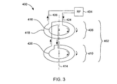
本発明の第1の局面によれば、プラズマ処理装置は、プラズマ処理システムのプロセスチャンバの内部において方位角について対称な(azimuthally symmetric)電界が誘導されるように、マルチターンアンテナ構成が設けられる。図3および4は、本発明のある実施形態によるマルチターンアンテナ構成400を示す。マルチターンアンテナ構成400は、RF電源404に動作可能に結合されたマルチターンアンテナ402を含み、これらは図2に示されるアンテナ210およびRF電源214にそれぞれ対応する。
According to a first aspect of the present invention, the plasma processing apparatus is provided with a multi-turn antenna configuration such that an azimuthally symmetric electric field is induced inside the process chamber of the plasma processing system. 3 and 4 illustrate a
前述のように、もしアンテナ長が波長に対して短いなら、電力結合の伝送線路記述はもはや適切ではなく、電力結合は集中定数回路要素として振る舞う。したがってマルチターンアンテナ402は、伝送されるエネルギーの波長よりも短い長さを持つように構成される。アンテナ長を短くすることによって、定在波パターン中に作られる節がより少なくなり、その結果、アンテナの方位角方向における高電圧および低電圧領域が実質的に減らされる。
As mentioned above, if the antenna length is short with respect to wavelength, the transmission line description for power coupling is no longer appropriate and power coupling behaves as a lumped circuit element. Accordingly, the
マルチターンアンテナ構成は、発生する電磁界が単一のターンアンテナからであるように見えるよう、互いに近接して配置された複数のターン群を持つよう好ましくは構成される。より具体的には、ターン群を互いに近接して配置することによってアンテナの容量を作る電流は増す。例えばもしアンテナが互いに近接した4ターンであるなら、プラズマを通る電流は、アンテナ中のそれの約4倍の強さになる傾向がある。対応して、この集中した電流は、より均一な集中したプラズマにつながる。その結果、アンテナの直径は、プロセスチャンバの直径に対してより小さくでき、よってこれでアンテナ長を小さくできる。アンテナの実際のサイズは、以下に詳細に説明される。 The multi-turn antenna configuration is preferably configured to have a plurality of turns arranged in close proximity to each other so that the generated electromagnetic field appears to be from a single turn antenna. More specifically, the current that creates the capacity of the antenna is increased by arranging the groups of turns close to each other. For example, if the antenna is four turns close to each other, the current through the plasma tends to be about four times as strong as that in the antenna. Correspondingly, this concentrated current leads to a more uniform concentrated plasma. As a result, the diameter of the antenna can be made smaller than the diameter of the process chamber, thus reducing the antenna length. The actual size of the antenna is described in detail below.
マルチターンアンテナ402は、実質的に円形であり、少なくとも第1平面内の同心円ループ群406の第1ペア、および第2平面内の同心円ループ群410の第2ペアを含む。好ましくは同心円ループ406の第1ペアおよび同心円ループ410の第2ペアは、実質的に同一であり、アンテナ軸414に沿って互いに対称的にアラインされる。実質的に円形のアンテナは、実質的に円形の電界を発生し、その結果、実質的に円形のプラズマを発生することに注意されたい。したがって、プロセスチャンバおよび基板が円形であるので、実質的に円形のプラズマはより均一な処理を基板表面において実行できる傾向にあるというロジックが成り立つ。
本発明は実質的に円形であるとして示され説明されてきたが、チャンバ設計におけるある程度の非対称性を持ったディスプレイまたは補償のためなど、異なる形状の基板を必要とする応用例のための代替の形状が使用されえることが理解されなければならない。例として、上述と同じ原理に従う楕円形、または円形の角を持つ長方形もうまく機能しえる。 Although the present invention has been shown and described as being substantially circular, an alternative for applications requiring differently shaped substrates, such as for displays or compensation with some asymmetry in the chamber design. It should be understood that shapes can be used. By way of example, an ellipse following the same principle as described above, or a rectangle with circular corners may work well.
さらに同心円ループ群406の第1ペアは、好ましくは同心円ループ群408の第2ペア上にスタックされる。単一平面アンテナは典型的には容量結合が増すが、これは端子電圧および全ての電圧の節が窓の直近に存在するからである。しかしスタックされたアンテナ、および同心円ループ群の第1ペアおよび同心円ループ群の第2ペア間の対称的なアライメントのために、高端子電圧は、同心円ループ群の第2ペアによって効果的に遮蔽される。より具体的には、第1同心円ループおよびプラズマ間に典型的に起こる電圧降下(例えば容量性結合)が大きく低減されるが、これは同心円ループ群の第2ペアが、電圧降下の伝導パスを提供し、よって電圧降下がプラズマに相互作用を及ばさないからである。
Further, the first pair of
さらに、同心円ループ群406の第1ペアは、好ましくは第1ターン416および第4ターン418を含み、同心円ループ群410の第2ペアは、好ましくは第2ターン420および第3ターン422を含む。さらに第1ターン416は実質的に第2ターン420と同一で、第2ターン420の上に配置され、第4ターン418は実質的に第3ターン422と同一で、第3ターン422の上に配置される。
Further, the first pair of
第1ターン416は動作可能に第2ターン420に結合され、第2ターン420は動作可能に第3ターン422に結合され、第3ターン422は動作可能に第4ターン418に結合され、それぞれのターンは、電流の向きがアンテナ軸414の周りに同じ向きになるよう構成される。ある実施形態において、マルチターンアンテナは、単一の伝導要素から形成される。しかしこれは限定ではなく、マルチターンアンテナは構造的にかつ電気的に互いに結合された別個の部品から形成されえる。さらにマルチターンアンテナ402は、入力リード424および出力リード426を含む。入力リード424は動作可能に第1ターン416に結合され、出力リード426は動作可能に第4ターン418に結合される。したがってRF電圧を入力リード424および出力リード426の間に印加することによって、RF電流がマルチターンアンテナ402を通して流れるよう構成される。
The
さらに図3および図4を参照して、第4ターン418は、第1ターン416よりもより大きい直径を持ち、第3ターン422は、第2ターン420よりもより大きい直径を持つ。外側ターン(例えば第3および第4ターン)はより大きい直径を持つが、それらは好ましくは内周ターン(例えば第1および第2ターン)の近傍に配置される。すなわち第4ターン418は好ましくは第1ターン416の近傍に配置され、第3ターン418は好ましくは第2ターン420の近傍に配置される。これらの近接配置によって、マルチターンアンテナは単一ターンアンテナのような形状であり、また単一ターンアンテナのように振る舞う(例えば実質的にターン間にはスペースがない)。したがって半径方向の高および低電流領域は実質的に低減される。
Still referring to FIGS. 3 and 4, the
当業者にはよく知られるように、2つの導体間の小さいスペースは、典型的には2つの導体間でアークを発生する。したがって外側および内側ターン間のスペースは、アークを起こさない距離に限定される。しかし本発明のある実施形態において、内側および外側ターンが互いになるべく接近して配置されつつも、一方で、実質的に内側および外側ターン間のアークを防止することを可能にするために、このスペースは誘電体材料で埋められる。例として、約0.2から約1cmの間のスペースを持つテフロン(登録商標)またはセラミック材料がうまく機能する。 As is well known to those skilled in the art, a small space between two conductors typically generates an arc between the two conductors. Thus, the space between the outer and inner turns is limited to a distance that does not cause an arc. However, in certain embodiments of the present invention, this space may be used to allow the inner and outer turns to be placed as close as possible to one another while substantially preventing arcing between the inner and outer turns. Is filled with a dielectric material. As an example, Teflon or ceramic material with a space between about 0.2 and about 1 cm works well.
さらにマルチターンアンテナは一般に銅から形成される。ある実現例では、マルチターンアンテナは銀でコーティングされた銅から形成される。しかしマルチターンアンテナは銅または銀でコーティングされた銅に限定はされず、任意の適切な伝導性金属が用いられえることに注意されたい。ある実施形態において、アンテナループの断面は、それぞれループを窓およびそれぞれの他のループに対して繰り返し位置決めするのが楽なように長方形である。しかしこれは限定ではなく、他の断面形状およびサイズが用いられえる。代替としては、アンテナループは、温度制御を促進するために(すなわちその中を流体を流すために)空洞のある導体から形成されえる。 Furthermore, the multi-turn antenna is generally formed from copper. In one implementation, the multi-turn antenna is formed from copper coated with silver. However, it should be noted that the multi-turn antenna is not limited to copper coated with copper or silver, and any suitable conductive metal can be used. In some embodiments, the cross section of the antenna loop is rectangular so that it is easy to repeatedly position each loop relative to the window and each other loop. However, this is not a limitation and other cross-sectional shapes and sizes can be used. Alternatively, the antenna loop may be formed from a hollow conductor to facilitate temperature control (ie, to flow fluid therethrough).
マルチターンアンテナの全体のサイズ、すなわち外側直径について、アンテナがプロセスチャンバの断面よりも小さい大きさに設定されることが一般には好ましく(絶対に必要というわけではなく)、これはプラズマを基板上の領域に集中させた状態に維持し、チャンバ壁への不要なプラズマ拡散を避けるためである。このプラズマ拡散は、プラズマ処理システムを動作させる電力をより多く必要とし、壁のエロージョンを増加させるなどの不利益をもたらす。さらにプラズマのサイズは一般に用いられるアンテナのサイズに対応するので、よってマルチターンアンテナは、均一なエッチング速度を実現するために、基板の直径と実質的に同様な外側直径を持たなければならない。例として、基板のサイズは典型的には約6から約12インチの間であり、よってある実施形態では、マルチターンアンテナは、約6および約12インチの間の外側直径を持つ。 For the overall size of the multi-turn antenna, i.e. the outer diameter, it is generally preferred (though not absolutely necessary) that the antenna is set to be smaller than the cross section of the process chamber, which causes the plasma on the substrate. This is to maintain a concentrated state in the region and avoid unnecessary plasma diffusion to the chamber wall. This plasma diffusion requires more power to operate the plasma processing system and has disadvantages such as increased wall erosion. Furthermore, since the size of the plasma corresponds to the size of the commonly used antenna, the multi-turn antenna must therefore have an outer diameter that is substantially similar to the diameter of the substrate in order to achieve a uniform etch rate. By way of example, the size of the substrate is typically between about 6 and about 12 inches, and thus in some embodiments, the multi-turn antenna has an outer diameter between about 6 and about 12 inches.
さらに詳述すれば、増加された電流容量のために、すなわちマルチターンアンテナは単一のターンのように振る舞うので、マルチターンアンテナは基板よりも小さく構成されえる。すなわち電流のより高い集中は、基板を処理するのに充分に大きいプラズマを発生する傾向にある。しかしより小さいアンテナの使用は全ての処理に必要とされるわけではなく、アンテナは基板よりも大きく構成されえることに注意されたい。しかしもし高度な均一性が重要であるなら、より小さいアンテナの使用はかなり有用でありえる。例として、12インチの基板を処理するためには、アンテナの直径は約6から約15インチの間で構成されえ、好ましくは約7から約11インチである。しかしこれは限定ではなく、アンテナの実際のサイズは、基板の特定のサイズにしたがって(例えばアンテナサイズはより小さいまたは大きい基板が関連するときに必要に応じて大きさを変更されえる)、またはそれぞれのプラズマ処理システムの特定の設計にしたがって変化しえる。 More specifically, because of the increased current capacity, i.e., the multi-turn antenna behaves like a single turn, the multi-turn antenna can be made smaller than the substrate. That is, the higher concentration of current tends to generate a plasma that is large enough to process the substrate. However, it should be noted that the use of smaller antennas is not required for all processes and the antenna can be configured larger than the substrate. However, if a high degree of uniformity is important, the use of smaller antennas can be quite useful. As an example, to process a 12 inch substrate, the antenna diameter may be comprised between about 6 and about 15 inches, and preferably is about 7 to about 11 inches. However, this is not a limitation and the actual size of the antenna depends on the specific size of the board (eg the antenna size can be resized as needed when smaller or larger boards are involved), or each Can vary according to the particular design of the plasma processing system.
用いられるRF周波数について、一般的なガイドラインとして、より低いRF周波数(例えば13MHz未満)は、定在波の効果を減らすことによって電力結合の伝送線路特性の効果を低減させる傾向にある。すなわちより低い周波数は、アンテナの方位角についての潜在的な非対称結合特性をより緩和する傾向にある。さらにより低いRF周波数において、アンテナおよびプラズマ間の容量性結合も緩和され、よって結合窓のイオン衝突が減少する。したがってRF電源の周波数は一般に約13MHz以下に構成され、好ましくは約0.4MHzおよび約13MHzの間であり、さらに好ましくは約4MHzである。より低い周波数の使用は全ての処理に必要とされるわけではないことに注意されたい。しかしもし高度の均一性が重要であるなら、低い周波数の使用はかなり有用でありえる。 As a general guideline for the RF frequencies used, lower RF frequencies (eg, less than 13 MHz) tend to reduce the effect of power coupled transmission line characteristics by reducing the effect of standing waves. That is, lower frequencies tend to more relax the potential asymmetric coupling characteristics for antenna azimuth. At even lower RF frequencies, capacitive coupling between the antenna and the plasma is also relaxed, thus reducing ion collisions in the coupling window. Accordingly, the frequency of the RF power supply is generally configured to be about 13 MHz or less, preferably between about 0.4 MHz and about 13 MHz, and more preferably about 4 MHz. Note that the use of lower frequencies is not required for all processes. However, if a high degree of uniformity is important, the use of lower frequencies can be quite useful.
前述のように、本発明の第1の局面の効果は数多くある。異なる実施形態または実現例は、以下の効果の一つ以上を持ちえる。本発明の一つの効果は、方位角について対称的なプラズマがプロセスチャンバ内に作られることである。その結果、プロセス均一性を高くでき、これは基板スループットを増し、デバイス欠陥を減らし、処理されている基板の全体的な生産性を上げる。本発明の他の効果は、本発明のアンテナ構成はそれ自身で遮蔽でき、よってアンテナおよびプラズマ間の容量性結合を低減させる。対応して、結合窓のイオン衝突が低減され、よって結合窓の寿命が延び、イオン衝突に関連付けられた粒子コンタミネーションが低減される。 As described above, there are many effects of the first aspect of the present invention. Different embodiments or implementations may have one or more of the following effects. One advantage of the present invention is that a plasma symmetric about the azimuth is created in the process chamber. As a result, process uniformity can be increased, which increases substrate throughput, reduces device defects, and increases the overall productivity of the substrate being processed. Another advantage of the present invention is that the antenna configuration of the present invention can be shielded by itself, thus reducing capacitive coupling between the antenna and the plasma. Correspondingly, binding window ion collisions are reduced, thus extending the lifetime of the binding window and reducing particle contamination associated with ion collisions.
本発明の第2の局面によれば、プラズマ処理装置は、アンテナおよびプラズマ間の容量性結合を実質的に低減するために多層結合窓構成を備える。本発明のこの局面の議論を進めるために、図5は、本発明のある実施形態による多層結合窓構成500を示す。多層結合窓構成500は、図2の結合窓212に対応しえる。多層結合窓500は、少なくとも第1レイヤ504および第2レイヤ506を含む。好ましくは第1レイヤ504は第2レイヤ506に接着されている。ある実現例では、2つのレイヤは互いに熱的に接着される。しかしこれは限定ではなく、他の接着プロセスが用いられえることに注意されたい。代替としては、レイヤ間にギャップ、すなわち真空ギャップまたはレイヤ間をガスが流れるギャップが設けられえ、一方で、前述の利点をも享受できることに注意されたい。さらに第2レイヤ506は、好ましくはプロセスチャンバの内側周辺表面の一部を形成する。
According to a second aspect of the invention, the plasma processing apparatus comprises a multilayer coupling window configuration to substantially reduce capacitive coupling between the antenna and the plasma. To further discussion of this aspect of the invention, FIG. 5 shows a multi-layer
まず第2レイヤを参照すれば、第2レイヤは、その表面上での電位差を少なくする静電遮蔽として振る舞うよう構成される。さらに第2レイヤは、電気的に絶縁され、好ましくは、アンテナからプラズマへの誘導性RFエネルギーの透過を促進できる伝導性または半伝導性材料から形成されるよう構成される。さらに第2レイヤは、プロセスチャンバ内のプラズマに曝されるので、第2レイヤは好ましくはプラズマに実質的に耐えうる材料から形成される。好ましい実施形態において、第2レイヤは、シリコンカーバイド(SiC)から形成される。たいていの場合、SiCは、プラズマ処理の熱的、化学的、および物理的影響に耐えうる。さらにSiCは一般に誘電体として分類され、しかし電流の流れに対してある程度の抵抗を示す。抵抗特性は遮蔽効果を生むものであり、誘電体特性は誘導性結合を許すものである。 Referring first to the second layer, the second layer is configured to behave as an electrostatic shield that reduces the potential difference on its surface. Further, the second layer is electrically isolated and is preferably configured to be formed from a conductive or semiconductive material that can facilitate the transmission of inductive RF energy from the antenna to the plasma. Furthermore, since the second layer is exposed to the plasma in the process chamber, the second layer is preferably formed from a material that can substantially withstand the plasma. In a preferred embodiment, the second layer is formed from silicon carbide (SiC). In most cases, SiC can withstand the thermal, chemical, and physical effects of plasma processing. Furthermore, SiC is generally classified as a dielectric, but exhibits some resistance to current flow. The resistance characteristics produce a shielding effect, and the dielectric characteristics allow inductive coupling.
第2レイヤの抵抗は、静電遮蔽としてレイヤが機能することを確実にしつつ、一方で、誘導性電界に影響を与えないための重要なパラメータである。たいていの場合、本発明で用いられる特定の抵抗レンジは、結合窓が用いられるアンテナの具体的な寸法、電力結合の動作周波数、および第2レイヤの厚さに依存する。例として、約100Ω−cmから約10kΩ−cmがうまく機能する。しかしもし望まれるなら、第2レイヤ(例えばSiC)が誘電体層としてより振る舞うようにさせるために、抵抗は、106Ω−mより大きく構成されえる。 The resistance of the second layer is an important parameter to ensure that the layer functions as electrostatic shielding while not affecting the inductive electric field. In most cases, the particular resistance range used in the present invention depends on the specific dimensions of the antenna in which the coupling window is used, the operating frequency of the power coupling, and the thickness of the second layer. As an example, about 100 Ω-cm to about 10 kΩ-cm works well. However, if desired, the resistance can be configured to be greater than 10 6 Ω-m in order to make the second layer (eg, SiC) behave more as a dielectric layer.
理論によって拘束されたくないと願う反面、第2レイヤの電気抵抗は、プラズマを形成するのに用いられる処理ガスに等電位表面を提供すると信じられる。例えば、プラズマの点火後、第2レイヤ上の電位は、プラズマが第2レイヤの近傍に位置するために大きく下げられる。さらに容量性電圧分割器が一般に形成され、例えば一定の容量を持つ誘電体第1レイヤによって形成される上部と、および点火前には伝導性第2レイヤおよびチャンバ壁によって、点火後には伝導性第2レイヤおよびプラズマによって形成される下部とからなる。点火前にはこの下部は小さい容量を持ち、よって点火を助ける大きな電圧が存在する(例えば放電を開始するためには、容量性電界が典型的には必要である)。点火後には、この下部は、この電圧が大きく下げられる大きな容量を持ち、よって大きな容量性電力結合には結びつかない。 While wishing not to be bound by theory, it is believed that the electrical resistance of the second layer provides an equipotential surface for the process gas used to form the plasma. For example, after the plasma is ignited, the potential on the second layer is greatly reduced because the plasma is located near the second layer. In addition, a capacitive voltage divider is generally formed, for example by an upper part formed by a dielectric first layer having a constant capacity, and a conductive second layer and chamber wall before ignition, and a conductive second layer after ignition. It consists of two layers and a lower part formed by plasma. Prior to ignition, this lower part has a small capacity, so there is a large voltage to aid ignition (eg, a capacitive electric field is typically required to initiate discharge). After ignition, this lower part has a large capacity at which this voltage can be greatly reduced and thus does not lead to a large capacitive power coupling.
こんどは第1レイヤを参照すれば、この第1レイヤは好ましくは、アンテナからプラズマへの誘導性RFエネルギーの透過を促進できる誘電体材料から形成される。さらに第1レイヤは、構造的に真空を維持するよう充分な強度を持って、かつチャンバの定期的クリーニング中に容易に扱えるよう充分に堅固に構成される。さらに第1レイヤは、窓の温度制御を可能にする優れた熱的特性を持つ誘電体材料から一般に形成される。例として、窒化シリコン(SiN)または窒化アルミニウム(AlN)から形成された誘電体材料がうまく機能する。しかしこれは限定ではなく、他の材料も用いられえることに注意されたい。例えば、アルミナおよび石英もうまく機能する。 Referring now to the first layer, this first layer is preferably formed from a dielectric material that can facilitate the transmission of inductive RF energy from the antenna to the plasma. Furthermore, the first layer is structurally strong enough to maintain a vacuum structurally and is sufficiently rigid to be easily handled during periodic cleaning of the chamber. Furthermore, the first layer is generally formed from a dielectric material with excellent thermal properties that allows window temperature control. As an example, dielectric materials formed from silicon nitride (SiN) or aluminum nitride (AlN) work well. However, it should be noted that this is not a limitation and that other materials can be used. For example, alumina and quartz work well.
多層結合窓500の全体の厚さは、アンテナRFエネルギーをプラズマに効率的に伝送できるよう充分に薄くしつつ、処理中に発生する圧力および熱に耐えるのに充分なよう構成される。好ましくは、多層結合窓の厚さは、約0.5および約1インチの間である。より好ましくは、多層結合窓の厚さは、約0.8インチである。さらに第1レイヤ504は、第2レイヤ506よりも厚い厚さを持たなければならない。好ましくは、第1レイヤの厚さは、約0.5および約1インチの間である。より好ましくは、第1レイヤの厚さは、約0.6インチである。さらに第2レイヤの厚さは、好ましくは、約0.1および約0.5インチの間である。より好ましくは、第2レイヤの厚さは、約0.2インチである。レイヤの実際の厚さは、それぞれのレイヤに選ばれた具体的な材料にしたがって変更されえる。
The overall thickness of the
ある実施形態においては、第1レイヤをプラズマへの曝露から保護し、かつ基板と接触するプラズマ領域に純粋な材料(例えばSiC)が面するように、第2レイヤは第1レイヤ全体を覆う。しかしこれは限定ではなく、他の構成が使用されえることに注意されたい。例えば第2レイヤは、第1レイヤのうちのアンテナ付近のプラズマに面する部分だけを覆うように構成されえる。 In some embodiments, the second layer covers the entire first layer so that the first layer is protected from exposure to the plasma, and the pure material (eg, SiC) faces the plasma region in contact with the substrate. However, it should be noted that this is not a limitation and that other configurations can be used. For example, the second layer may be configured to cover only the portion of the first layer that faces the plasma near the antenna.
結合窓のサイズがプラズマ処理チャンバのサイズに等しくなければならないという条件は存在しないことに注意されたい。しかし一般に小さい結合窓はコストを下げ、特にSiCのような高価な材料が採用されるときにはそうである。ある実施形態においては、結合窓の形状は、アンテナ構成の形状と一致するように構成され、よって結合窓は実質的に円形である。他の実施形態においては、結合窓の外側寸法は、アンテナを囲みえる電気的に伝導性を持つ要素への結合を少なくするために、アンテナの外側寸法を少しの距離だけ超えて外に伸びるよう構成されえる。ある例では、結合窓の外側寸法は、アンテナの外側寸法を約1インチ超えて外に伸びるように構成されえる。さらに他の実施形態においては、結合窓は実質的にアンテナと同じ、すなわち輪状の形状を持ちえる。 Note that there is no requirement that the size of the coupling window must be equal to the size of the plasma processing chamber. However, generally small bond windows reduce costs, especially when expensive materials such as SiC are employed. In some embodiments, the shape of the coupling window is configured to match the shape of the antenna configuration, so that the coupling window is substantially circular. In other embodiments, the outer dimension of the coupling window extends beyond the outer dimension of the antenna by a small distance to reduce coupling to an electrically conductive element surrounding the antenna. Can be configured. In one example, the outer dimension of the coupling window can be configured to extend outwardly about one inch beyond the outer dimension of the antenna. In still other embodiments, the coupling window may have substantially the same shape as the antenna, i.e., a ring shape.
採用される誘電体特性(例えば誘電率)について、一般的なガイドラインとしては、より低い誘電率、例えば約10未満が、定在波効果を減少させることによって電力結合の伝送線路特性の効果を減らす傾向にある。より具体的には、より低い誘電率は、伝送されるエネルギーの波長をより長くする傾向があり、これはアンテナを見かけ上短くし、よって定在波パターン中に少ししか節を作らないことになる。したがって、より低い誘電率は、アンテナの任意の潜在的な方位角について非対称な結合特性を緩和する傾向にある。 As a general guideline for the dielectric properties employed (eg, dielectric constant), lower dielectric constants, eg, less than about 10, reduce the effect of power coupled transmission line characteristics by reducing the standing wave effect. There is a tendency. More specifically, a lower dielectric constant tends to make the wavelength of the transmitted energy longer, which apparently shortens the antenna and thus creates fewer nodes in the standing wave pattern. Become. Thus, the lower dielectric constant tends to relax the asymmetric coupling characteristics for any potential azimuth angle of the antenna.
ある実施形態においては、結合窓の全体の誘電率は、好ましくは約10以下に構成される。低い誘電率の使用は全ての処理について必要とされるわけではないことに注意されたい。実際、方位角について高度に対称的である要求と、構造的および熱的設計の容易さとの間の妥協が典型的には必要となる。しかしもし高度な均一性が重要であるなら、低い誘電率の使用はかなり有用でありえる。 In some embodiments, the overall dielectric constant of the coupling window is preferably configured to be about 10 or less. Note that the use of a low dielectric constant is not required for all processes. Indeed, a compromise between the requirement of being highly symmetric with respect to azimuth and the ease of structural and thermal design is typically required. However, if a high degree of uniformity is important, the use of a low dielectric constant can be quite useful.
上述からわかるように、本発明の第2の局面の効果は多く存在する。異なる実施形態または実現例は、以下の効果のうちの一つ以上を持ちえる。例えば本発明は、アンテナおよびプラズマ間の容量性結合を実質的に減少する結合窓を提供する。その結果、プラズマのバラツキは実質的に減少される。例えば誘導性結合係数は典型的には維持され、結合窓のイオン衝突は低減され、プラズマ発生のためにより多くの電力が利用可能であり、すなわち与えられた電力についてはより高いプラズマ密度が得られる。さらにイオン衝突が低減されるので、イオン衝突と関連する粒子コンタミネーションが一般に低減され、その結果、変動する厚さの窓(すなわち材料が堆積したり除去されたりする)に関連するプロセスのバラツキが低減される。さらに本発明は、純粋な材料、すなわちSiCを利用するので、プロセスのバラツキを低減する傾向にある。 As can be seen from the above, there are many effects of the second aspect of the present invention. Different embodiments or implementations may have one or more of the following effects. For example, the present invention provides a coupling window that substantially reduces capacitive coupling between the antenna and the plasma. As a result, plasma variation is substantially reduced. For example, the inductive coupling coefficient is typically maintained, ion bombardment of the coupling window is reduced, and more power is available for plasma generation, i.e. higher plasma density is obtained for a given power . Further, since ion collisions are reduced, particle contamination associated with ion collisions is generally reduced, resulting in process variations associated with variable thickness windows (ie, material is deposited and removed). Reduced. Furthermore, the present invention utilizes a pure material, i.e. SiC, and therefore tends to reduce process variation.
さらに、上述のマルチターンアンテナおよび多層結合窓と共に、プラズマ処理システム中の基板の均一な処理をより向上させるために、追加の要素が採用されえることが考えられる。例として、結合窓およびマルチターンアンテナの近傍領域のプロセスチャンバ内での静磁界の半径方向のバラツキを制御するために、磁気構成物がマルチターンアンテナと共に構成されえる。そのような磁気構成物の例は、1999年11月15日に出願された「IMPROVED PLASMA PROCESSING SYSTEMS AND METHODS THEREFOR」と題された同時係属中の米国特許出願第09/439,661号に見られ、ここで参照によって援用される。 In addition, it is contemplated that additional elements may be employed with the multi-turn antenna and multi-layer coupling window described above to further improve the uniform processing of the substrate in the plasma processing system. As an example, a magnetic component can be configured with a multi-turn antenna to control radial variations in the static magnetic field within the process chamber in the vicinity of the coupling window and multi-turn antenna. Examples of such magnetic components can be found in co-pending US patent application Ser. No. 09 / 439,661, filed Nov. 15, 1999, entitled “IMPROVED PLASMA PROCESSING SYSTEMS AND METHODS THEREFOR”. , Incorporated herein by reference.
微小寸法が小さくなり続けるにつれて、方位角について対称的でないプラズマの許容誤差も小さくなる。短絡を防ぐために、アンテナターンは不完全であり、アンテナループの端部の間にはギャップが存在する。そのようなギャップは、プラズマが方位角について対称的であることを阻止しえる。図6は、ギャップ608を持つ、完全でないアンテナターン604の概略図である。第1角616によって定義される第1方位角扇形部612は、ギャップ608を含む。第2角624によって定義される第2方位角扇形部620は、ギャップ608を含まない。ギャップ608は、第1方位角扇形部612内のRF電力が第2方位角扇形部620内のRF電力よりも小さくなるように働く。ギャップをブリッジするために、さまざまな電流を流す要素が用いられてきた。そのようなブリッジ要素の非対称性によって、そのような要素は所望の均一性を提供できなくなる。
As micro-dimensions continue to get smaller, the tolerance of plasma that is not symmetrical about azimuth also becomes smaller. In order to prevent a short circuit, the antenna turn is incomplete and there is a gap between the ends of the antenna loop. Such a gap can prevent the plasma from being symmetric about the azimuth. FIG. 6 is a schematic diagram of an
図7は、本発明のある実施形態によって提供されるマルチターンアンテナ700の透視図である。マルチターンアンテナ700は、第1ターン704、第2ターン708、第3ターン712、および第4ターン716を備える。入力バス720は、第1ターン704に接続される。出力バス724は、第4ターン712に接続される。図8は、図7の破断面728の拡大された概略上面図であり、第3ターン712、第4ターン716、および出力バス724の一部を示す。第1ターン、第2ターン、および入力バス720は、図8においては簡潔さのために示されない。図9は、第3ターン712だけの上面図である。図8および図9に示されるように、第3ターン712は、第1端部804および第2端部808を持ち、ここで第3ターン712の第1端部804および第2端部808は第3ターンギャップ812によって分離される。第3ターン712は、アンテナ軸904上に中心付けられる。第3ターン712の半径906は、アンテナ軸904から第3ターン712上の点まで伸びる。第3ターン712の円周908は、第1端部804から第3ターン712に沿って第3ターンの第2端部808に向かい、ギャップ812を横切って第3ターン712の第1端部804に戻る第3ターンに沿う向きである。好ましくはギャップ812は、第3ターン712のうちのごく一部だけである。これらの図のいくつかは、ある要素をより明瞭に図示するために、ギャップ812のような要素は縮尺通りには描かれていない。示されるようにギャップ812は、アンテナ軸と角912を形成する。好ましくはギャップ812によって形成される角912は、7°未満である。より好ましくはギャップによって形成される角は、5°未満である。より好ましくはギャップによって形成される角は、3°未満である。第3ターンギャップ812の長さは、第3ターン712の円周に実質的に平行である。第3ターンの第1端部804の少なくとも一部とアンテナ軸904との間の距離は、第3ターンの第2端部808の少なくとも一部とアンテナ軸904との間の距離に等しい。これは、第3ターンの第1端部の内側部分と、第1端部の外側部分との間の点への半径は、第3ターンの第2端部の内側部分と、第3ターンの第2端部808の外側部分との間の点への半径に等しいことを意味する。螺旋の一部を形成するターンはこの定義には当てはまらないが、それは、螺旋のターンのうちの部分は、両方の端部が一致しないよう第1端部および第2端部が異なる半径を持つからである。より好ましくは、図9に示されるように第1端部804の半径は、第2端部808の半径に等しい。好ましくは、第3ターン712は実質的に円形である。より好ましくは、第3ターン712は示されるように円形である。
FIG. 7 is a perspective view of a
図10は、第4ターン716だけの上面図である。図8および図10に示されるように、第4ターン716は、第1端部816および第2端部820を有し、これらは第4ターンギャップ814によって分離される。第3ターン712は、第4ターン716から第3ターン−第4ターンギャップ828によって分離される。第3ターン−第4ターンギャップ828の長さは、第3ターン712および第4ターン716に対して半径方向であり、これは第3および第4ターン712、716の接線に実質的に垂直である。第4ターン716は、アンテナ軸904上に中心付けられる。第3ターン712および第4ターン716は、同心円状で同一平面上にあり、その結果、それらはアンテナ軸904上の同一の点の周りに中心付けられる。第4ターン716の半径1006は、アンテナ軸904から第4ターン716上の点へ伸び、その結果、第4ターン716は、第3ターン−第4ターンギャップ828のサイズにほぼ等しいだけ第3ターン712よりも大きい半径を持つ。第4ターン716の周囲1008は、第1端部816から第4ターン716に沿って第4ターンの第2端部820に向かい、ギャップ824を横切って第4ターン716の第1端部816に戻る第4ターンに沿う向きである。好ましくはギャップ824は、第4ターン716のうちのごく一部だけである。示されるようにギャップ824は、アンテナ軸と角1012を形成する。好ましくはギャップ824によって形成される角1012は、7°未満である。より好ましくはギャップによって形成される角は、5°未満である。より好ましくはギャップによって形成される角は、3°未満である。第4ターンギャップ824の長さは、第4ターン716の円周に実質的に平行である。この例では、第1端部816および第2端部820は、切り欠き角部1016を有する。第4ターンの第1端部816の少なくとも一部とアンテナ軸904との間の距離は、第4ターンの第2端部820の少なくとも一部とアンテナ軸904との間の距離に等しい。これは、第4ターンの第1端部の内側部分と、第1端部の外側部分との間の点への半径は、第4ターンの第2端部の内側部分と、第4ターンの第2端部820の外側部分との間の点への半径に等しいことを意味する。ここで第1端部の内側部分は、第1端部が切り欠きを作られなかったかのように、第1端部の切り欠き部1016を含むように定義され、第2端部の外側部分は、第2端部が切り欠きを作られなかったかのように、第2端部の切り欠き角部を含むように定義され、これはこれらの切り欠きがコネクタがそこにマウントされ、使用中にはこれら切り欠きが実際には埋められるからである。螺旋の一部を形成するターンはこの定義には当てはまらないが、それは、螺旋のターンのうちの部分は、両方の端部が一致しないよう第1端部および第2端部が異なる半径を持つからである。より好ましくは、図10に示されるように第1端部816の半径は、第2端部820の半径に等しい。好ましくは、第4ターン716は実質的に円形である。より好ましくは、第4ターン716は示されるように円形である。
FIG. 10 is a top view of only the
第3ターン−第4ターンコネクタ832は、電気的接続を第3ターン808の第2端部および第4ターン816の第1端部間に提供する。好ましい実施形態において、第3ターン−第4ターンコネクタ832は、スパニング部(spanning section)836、第3ターンコネクタレッグ840、および第4ターンコネクタレッグ844を備える。好ましくはスパニング部836は、スパニング部836に隣接する第3ターン712の周囲および第4ターン716の周囲に実質的に平行である。第3ターンコネクタレッグ840は、第3ターン712に対して実質的に半径方向である。第3ターンコネクタレッグ840は、第3ターンに対して実質的に半径方向であるとは、第3ターンコネクタレッグに隣接する第3ターンの部分の半径に実質的に平行であることを意味する。第4ターンコネクタレッグ844は、第4ターン716に対して実質的に半径方向である。示されるようにスパニング部836は、第3ターン712および第4ターン716のほぼ中間である。第3ターンコネクタレッグ840は、第3ターンギャップ812の端部に隣接する。第4ターンコネクタレッグ844は、第4ターンギャップ824の端部に隣接する。好ましい実施形態において、第3ターンギャップ812および第4ターンギャップ824は互いに隣接し、その結果、第3ターンギャップ812の端部は、破線850によって示されるように半径に沿い、第4ターンギャップ824の始点と一致する。これによりギャップは示されるように重なり合うことなく隣接する。他のバリエーションとしては、ギャップ812、814が、好ましくは0.0625インチ(1.5875mm)および−0.0625インチ(−1.5875mm)の間の距離だけ重なり合い、ここで負の値は、重なりが存在せずに代わりにギャップが離れており、その結果、第3ターンに沿って測定されると、第3ターンギャップの終点の半径および第4ターンギャップの始点の半径が0.0625インチより小さい値だけ離れていることを意味する。より好ましくは第3および第4ギャップの重なりは、0.005インチ(0.127mm)および−0.005インチ(−0.127mm)の間である。パーセンテージでいうと、第3および第4ターンギャップの重なりは、第3ターンギャップの長さの50%および−50%の間であり、ここで負の値は、重なりが存在せずに代わりにギャップが離れており、その結果、第3ターンに沿って測定されると、第3ギャップの終点の半径および第4ギャップの始点の半径が第3ターンギャップの長さの50%より小さい値だけ離れていることを意味する。より好ましくは、第3および第4ターンギャップの重なりは、第3ターンギャップの長さの25%および−25%の間である。最も好ましくは、第3および第4ターンギャップの重なりは、5%および−5%の間である。コネクタ832は、第3ターン712および第4ターン716と同一平面にある。
Third turn-
図11は、図7の切り欠き部728の拡大された概略上面図であり、第1ターン704、第2ターン708、および入力バス720の一部を示し、ここで第3ターン、第4ターン、および出力バスは簡単のために図11では示されない。図12は、第1ターン704単独の上面図である。図11および図12に示されるように、第1ターン704は、第1端部1104および第2端部1108を有し、ここで第1ターン704の第1端部1104および第2端部1108は、第1ターンギャップ1112によって分離される。第1ターン704は、アンテナ軸904上に中心付けられる。第1ターン704の半径1206は、アンテナ軸904から第1ターン704上の点まで伸びる。第1ターン704の円周1208は、第1端部1104から第1ターン704に沿って第1ターンの第2端部1108に向かい、ギャップ1112を横切って第1ターン704の第1端部1104に戻る第1ターンに沿う向きである。好ましくはギャップ1112は、第1ターン704のうちのごく一部だけである。示されるようにギャップ1112は、アンテナ軸と角1212を形成する。好ましくはギャップ1112によって形成される角1212は、7°未満である。より好ましくはギャップによって形成される角1212は、5°未満である。より好ましくはギャップによって形成される角は、3°未満である。第1ターンギャップ1112の長さは、第1ターン704の円周に実質的に平行である。第1ターンの第1端部1104の少なくとも一部とアンテナ軸904との間の距離は、第1ターンの第2端部1108の少なくとも一部とアンテナ軸904との間の距離に等しい。より好ましくは図12に示されるように第1端部1104の半径は、第2端部1108の半径に等しい。好ましくは第1ターン704は実質的に円形である。より好ましくは第1ターン704は示されるように円形である。
FIG. 11 is an enlarged schematic top view of the
図13は、第2ターン708単独の上面図である。図11および図13に示されるように、第2ターン708は、第1端部1116および第2端部1120を有し、ここで第2ターン708の第1端部1116および第2端部1120は、第2ターンギャップ1124によって分離される。第1ターン704は、第2ターン708から第1ターン−第2ターンギャップ1128によって分離される。第1ターン−第2ターンギャップ1128の長さは、第1および第2ターン704、708に対して半径方向である。第2ターン708は、アンテナ軸904上に中心付けられる。第1ターン704および第2ターン708同心状であり、その結果それらはアンテナ軸904上の同一の点の周りに中心付けられる。第2ターン708の半径1306は、アンテナ軸904から第2ターン708上の点まで伸び、その結果、第1ターン704の半径は第2ターン708の半径1306よりもほぼ第1ターン−第2ターンギャップ1128の長さだけ長い。第2ターン708の円周1308は、第1端部1116から第2ターン708に沿って第2ターンの第2端部1120に向かい、ギャップ1124を横切って第2ターン708の第1端部1116に戻る第2ターンに沿う向きである。好ましくはギャップ1124は、第2ターン708のうちのごく一部だけである。示されるようにギャップ1124は、アンテナ軸と角1312を形成する。好ましくはギャップ1124によって形成される角1312は、7°未満である。より好ましくはギャップによって形成される角1312は、5°未満である。より好ましくはギャップによって形成される角は、3°未満である。第2ターンギャップ1124の長さは、第2ターン708の円周に実質的に平行である。この例では、第1端部1116および第2端部1120は、切り欠き角部を有する。第2ターンの第1端部1116の少なくとも一部とアンテナ軸904との間の距離は、第2ターンの第2端部1120の少なくとも一部とアンテナ軸904との間の距離に等しい。より好ましくは図13に示されるように第1端部1116の半径は、第2端部1120の半径に等しい。好ましくは第2ターン708は実質的に円形である。より好ましくは第2ターン708は示されるように円形である。
FIG. 13 is a top view of the
第1ターン−第2ターンコネクタ1132は、第1ターンの第2端部1108および
第2ターンの第1端部1116間の電気的接続を提供する。好ましい実施形態においては、第1ターン−第2ターンコネクタ1132は、スパニング部1136、第1ターンコネクタレッグ1140、および第2ターンコネクタレッグ1144を備える。好ましくはスパニング部1136は、スパニング部1136に隣接する第1ターン704の周囲および第2ターン708の周囲に実質的に平行である。第1ターンコネクタレッグ1140は、第1ターン704に対して実質的に半径方向である。第2ターンコネクタレッグ1144は、第2ターン708に対して実質的に半径方向である。示されるようにスパニング部1136は、第1ターン704および第2ターン708のほぼ中間である。第1ターンコネクタレッグ1140は、第1ターンギャップ1112の端部に隣接する。第2ターンコネクタレッグ1144は、第2ターンギャップ1124の端部に隣接する。好ましい実施形態において、第1ターンギャップ1112および第2ターンギャップ1124は互いに隣接し、その結果、第1ターンギャップ1112の端部は、破線1150によって示されるように半径に沿い、第2ターンギャップ1124の始点と一致する。これによりギャップは示されるように重なり合うことなく隣接する。他のバリエーションとしては、ギャップ1112、1114が、好ましくは0.0625インチ(1.5875mm)および−0.0625インチ(−1.5875mm)の間の距離だけ重なり合い、ここで負の値は、重なりが存在せずに代わりにギャップが離れており、その結果、第1ターンに沿って測定されると、第1ターンギャップの終点の半径および第2ターンギャップの始点の半径が0.0625インチより小さい値だけ離れていることを意味する。より好ましくは第1および第2ギャップの重なりは、0.005インチ(0.127mm)および−0.005インチ(−0.127mm)の間である。パーセンテージでいうと、第1および第2ターンギャップの重なりは、第1ターンギャップの長さの50%および−50%の間であり、ここで負の値は、重なりが存在せずに代わりにギャップが離れており、その結果、第1ターンに沿って測定されると、第1ギャップの終点の半径および第2ギャップの始点の半径が第1ギャップの長さの50%より小さい値だけ離れていることを意味する。より好ましくは、第1および第2ターンギャップの重なりは、第1ターンギャップの長さの25%および−25%の間である。最も好ましくは、第1および第2ターンギャップの重なりは、5%および−5%の間である。コネクタ1132は、第1ターン704および第2ターン708と同一平面内にあり、好ましくは第1ターン704および第2ターン708と同一の高さを有する。
First turn-
図14は、部分728の概略透視図であり、第1ターン704、第2ターン708、第3ターン712、第4ターン716、入力バス720、出力バス724、第1ターン−第2ターンコネクタ1132、第3ターン−第4ターンコネクタ832、および第2ターン−第3ターンコネクタ1404を示す。
FIG. 14 is a schematic perspective view of the
動作時においてアンテナ700は、プラズマ処理チャンバ200内で使用されえる。電流「I」は、RF電源214から入力バス720を通って第1ターン704の第1端部1104に流れる。電流は、第1ターン704の第1端部1104から第1ターン704の第2端部1108に流れる。第1ターンギャップ1112は、第1ターンの第1端部および第1ターンの第2端部間の短絡を防止するために設けられる。それから電流は第1ターンの第2端部から第1ターンコネクタレッグ1140を通って第1ターンに対して実質的に半径方向の向きに流れ、それからスパニング部1136に沿ってスパニング部1136に隣接する第1ターン704および第2ターン708の円周に実質的に平行な向きに流れる。それから電流は、第2ターンコネクタレッグ1144を通って第2ターンに対して実質的に半径方向の向きに第2ターン708の第1端部1116に流れる。電流は、第2ターン708の第1端部1116から第2ターン708の第2端部1120に流れ、それから第2ターン−第3ターンコネクタ1404を通って第3ターン712の第1端部804に流れる。電流は、第3ターンの第1端部804から第3ターン712の第2端部808に流れる。第3ターンギャップ812は、第3ターン804の第1端部および第3ターン808の第2端部間の短絡を防止するために設けられる。電流はそれから第3ターン808の第2端部から第3ターンコネクタレッグ840を通って第3ターンに対して実質的に半径方向の向きに流れ、それからスパニング部836に沿ってスパニング部836に隣接する第3ターン712および第4ターン716の円周に実質的に平行な向きに流れる。それから電流は、第4ターンコネクタレッグ844を通って第4ターンに対して実質的に半径方向の向きに第4ターン716の第1端部816に流れる。電流はそれから、第4ターン816の第1端部から第4ターン820の第2端部に流れ、出力バス724を通って流れる。RF発生器は、電流「I」が交番する向きに流れるようにする。
In operation, the
第1ターン−第2ターンコネクタ1132のスパニング部1136は、第1ターンギャップ1112に隣接する第1ターンに実質的に平行で第1ターン704と同一平面内にある電流パスを提供する。さらに第1ターン−第2ターンコネクタ1132のスパンニング部1136は、第2ターンギャップ1124に隣接する第2ターン708に実質的に平行で第2ターン708と同一平面内にある電流パスを提供する。第1ターンギャップ1112および第2ターンギャップ1124を、これらが互いに隣接し、しかし重なり合わないように配置することによって、第1ターン704、第2ターン708、およびスパニング部1136は、ギャップまたはある位置で3つの電流を生じる重なりがない完全なループの形で2つのカレントパスを提供する。実現するにあたり小さいギャップまたは重なりが生じえるが、このようなギャップまたは重なりを最小化することが方位角について均一なRF励起を提供し、それにより均一なプラズマを発生するためには望ましい。スパニング部1136は、第1および第2ターン704、708間にあり、その結果、スパニング部1136によって提供される電流パスは第1ターン704および第2ターン708に近い。好ましくは、スパンニング部1136は、第1ターン704および第2ターン708間の実質的に中間であり、方位角についてより均一なRF励起を提供しつつ、かつ一方では第1ターン704および第2ターン708間のギャップを維持する。
The spanning
第3ターン−第4ターンコネクタ832のスパニング部836は、第3ターンギャップ812に隣接する第3ターンに実質的に平行で第3ターン712と同一平面内にある電流パスを提供する。さらに第3ターン−第4ターンコネクタ832のスパンニング部836は、第4ターンギャップ824に隣接する第4ターン716に実質的に平行で第4ターン716と同一平面内にある電流パスを提供する。第3ターンギャップ812および第4ターンギャップ824を、これらが互いに隣接し、しかし重なり合わないように配置することによって、第3ターン712、第4ターン716、およびスパニング部836は、ギャップまたはある位置で3つの電流を生じる重なりがない完全なループの形で2つのカレントパスを提供する。実現するにあたり小さいギャップまたは重なりが生じえるが、このようなギャップまたは重なりを最小化することが方位角について均一なRF励起を提供し、それにより均一なプラズマを発生するためには望ましい。スパニング部836は、第3および第4ターン712、716間にあり、その結果、スパニング部836によって提供される電流パスは第3ターン712および第4ターン716に近い。好ましくは、スパンニング部836は、第3ターン712および第4ターン716間の実質的に中間であり、方位角についてより均一なRF励起を提供しつつ、かつ一方では第3ターン712および第4ターン716間のギャップを維持する。
The spanning
第1ターンコネクタレッグ1140を第1ターン704の半径に沿って、第1ターン704の平面内に配置することによって、第1ターンコネクタレッグ1140を通って流れるRF励起によって生じた電流からの破壊(disruption)が最小にされる。これは、第1ターンコネクタレッグ1140を第1ターン704と同一の平面内に設けることによって第1ターンコネクタレッグの長さが最小化されえるようにすることで部分的には達成される。さらに第1ターンコネクタレッグ1140を第1ターン704に対して半径方向に設けることによっても、第1ターンコネクタレッグ1140からのRFの破壊(disruption)を最小化しえる。これらの理由のために、第2ターンコネクタレッグ1144は、第2ターン708に対して実質的に半径方向であり、スパニング部1136に対して実質的に垂直方向であり、第3ターンコネクタレッグ840は、第3ターン712に対して実質的に半径方向であり、スパニング部836に対して実質的に垂直方向であり、第4ターンコネクタレッグ844は、第4ターン716に対して実質的に半径方向であり、スパニング部836に対して実質的に垂直方向である。
By disposing the first
ギャップを有するそれぞれのターンは、ループの端部を分離するギャップを有するシングルループを作る。この構成は、小さなギャップを持つ個々のループ群が用いられず、それぞれのループの端部が異なる半径である螺旋を用いる他のアンテナとは異なる。 Each turn with a gap creates a single loop with a gap separating the ends of the loop. This configuration differs from other antennas that use a helix in which individual loop groups with small gaps are not used and the ends of each loop are of different radii.
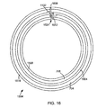
好ましい実施形態においては、アークを防止するために絶縁体が設けられる。図15は、第3ターン712、第4ターン716、および本発明の好ましい実施形態において用いられえる中央絶縁体1504上に取り付けられた第3ターン−第4ターンコネクタ832の上面図である。中央絶縁体1504は、ベースリング1508および上部リッジリング1512を備える。第3ターンギャップ絶縁体1516および第4ターンギャップ絶縁体1520も上部リッジを構成し、これらは上部リッジリング1512に接続される。ベースリング1508中のギャップ1524は、第2ターン−第3ターンコネクタのための通路を提供する。
In a preferred embodiment, an insulator is provided to prevent arcing. FIG. 15 is a top view of a third turn-
図16は、第1ターン704、第2ターン708、および中央絶縁体1504上に取り付けられた第1ターン−第2ターンコネクタ1132の上面図である。中央絶縁体1504はさらに底部リッジリング1604を備える。第1ターンギャップ絶縁体1608および第2ターンギャップ絶縁体1612も底部リッジを構成し、これらは底部リッジリング1604に接続される。外側リッジ1616は、第1ターン704の周囲に配置される。第2ターン−第3ターンコネクタのための通路を提供するギャップ1524は、ベースリング1508内に示される。
FIG. 16 is a top view of the first turn-
図17は、底部絶縁体1704の上面図である。底部絶縁体1704は、リングの形状をしており、中央溝1708、第1ターン溝1712、第2ターン溝1716、内側リッジ1720および外側リッジ1724を有する。
FIG. 17 is a top view of the
図18は、切断線18−18に沿った図17の底部絶縁体1704の断面図であり、これは第1ターン704、第2ターン708、第3ターン712、第4ターン716およびそこに取り付けられた中央絶縁体1504を有する。中央絶縁体1504の底部リッジリング1604は、底部絶縁体1704の中央溝内に取り付けられる。第1ターン704は、第1ターン溝1712内に取り付けられる。第2ターン708は、第2ターン溝1716内に取り付けられる。中央絶縁体1504の上部リッジリング1512は、第3ターン712および第4ターン716間のギャップを埋め、このギャップはアークを防止するのに充分な長さである。上部リッジリング1512は、第3ターン712および第4ターン716の上を伸び、その結果、上部リッジリング1512の表面に沿った、第3ターン712から第4ターン716までの距離は、アークを防止するのに必要とされる最小表面距離よりも大きい。底部絶縁体1704はファラデーシールド1804上に配置されえる。
18 is a cross-sectional view of the
図22は、ファラデーシールド1804の上面図である。ファラデーシールド1804は、結合の方位角についてのバラツキをさらに最小化し、容量性結合の程度を制御するために設けられえる。これは、ファラデーシールド1804をグラウンドに落とすか、特定の電圧をファラデーシールドに印加するか、またはファラデーシールドをフローティング状態にするかのいずれかによって実現されえる。アンテナのフットプリントがリングの形状であるので、ファラデーシールド1804はアンテナのフットプリントと一致するリング形状でありえる。好ましい実施形態においては、ファラデーシールド1804は、アンテナのフットプリントよりもわずかに大きく、リングの一部を横切る少なくとも一つの半径方向スロット2204を有するリング形状の伝導体材料である。図18は、ファラデーシールド1804の幅がアンテナの幅よりもわずかに大きいことを示す。他の好ましい実施形態においては、一つより多いスロットが設けられる。
FIG. 22 is a top view of the
図19は、入力バス720および出力バス724の切り欠き透視図である。この実施形態においては、入力バス720は、テーパが付けられた入力伝導バー1908に接続された入力コネクタ1904を備える。出力バス724は、テーパが付けられた出力伝導バー1916に接続された入力コネクタ1912を備える。テーパが付けられた伝導バー1908およびテーパが付けられた伝導バー1916は示されるようにアラインされ、互いに近接して配置される。I字形の誘電体部品1924がテーパが付けられた入力伝導バー1908およびテーパが付けられた出力伝導バー1916の間に配置され、テーパが付けられた入力伝導バー1908およびテーパが付けられた出力伝導バー1916の間でアークが発生することを防止する。テーパが付けられた入力伝導バー1908およびテーパが付けられた出力伝導バー1916のアライメントおよび近接配置は、テーパが付けられた入力伝導バー1908およびテーパが付けられた出力伝導バー1916によって発生されえるRF非対称性を最小化するのに役立つ。
FIG. 19 is a cutaway perspective view of the
本発明の実施形態においては、約600ボルトの電圧のとき、第3ターンギャップ812および第4ターンギャップ824は約0.125インチ(3.175mm)である。第3ターン712の第1端部804および第2端部808間の絶縁体1504の表面に沿ったパスの長さは、約0.25インチ(6.35mm)である。図18に示されるように絶縁体1504の表面に沿ったパスの長さは、絶縁体をターン端部を超えて伸ばすことによって長くすることができる。
In an embodiment of the present invention, the
図20は、RF電源2004に接続されたアンテナ構成2000の他の実施形態の概略図である。この実施形態においては、アンテナ構成は、第1ループ2006および第2ループ2010を備える。第1ループ2006は、第1ターン2016および第2ターン2018を備える。第2ループ2010は、第3ターン2020および第4ターン2022を備える。入力フィード2026は、RF電源2004から第1ターン2016の第1端部へ提供される。出力フィード2028は、第4ターン2022からRF電源2004へ接続される。第1スパニング部2032は、第3ターン2020および第4ターン2022の間に接続され、第1ターン2016および第2ターン2018と同一平面にあり、第1ターン2016のギャップおよび第2ターン2018のギャップをつなぐ。第3ターンレッグコネクタ2034は、第1スパニング部2032の第1端部を第3ターン2020に接続する。第4ターンレッグコネクタ2036は、第1スパニング部2032の第2端部を第4ターン2022に接続する。第2スパニング部2044は、第1ターン2016および第2ターン2018の間に接続され、第3ターン2020および第4ターン2022と同一平面にあり、第3ターン2020のギャップおよび第4ターン2022のギャップをつなぐ。第1ターンレッグコネクタ2046は、第2スパニング部2044の第1端部を第1ターン2016に接続する。第2ターンレッグコネクタ2048は、第2スパニング部2044の第2端部を第2ターン2018に接続する。第2ターン−第3ターンコネクタ2050は、第2ターン2018を第3ターン2020に接続する。以前の実施形態において説明されたように、ギャップは最小化される。また前述のように好ましくはそれぞれのターンのギャップは、7°未満の中心角をなす。より好ましくはそれぞれのターンのギャップは、5°未満の中心角をなす。最も好ましくはそれぞれのターンのギャップは、3°未満の中心角をなす。さらに第1ターンのギャップおよび第2ターンのギャップは、第1ターンのギャップ長の50%から−50%の間の範囲で重なり合い、第3ターンのギャップおよび第4ターンのギャップは、第3ターンのギャップ長の50%から−50%の間の範囲で重なり合う。より好ましくは、第1ターンのギャップおよび第2ターンのギャップは、第1ターンのギャップ長の25%から−25%の間の範囲で重なり合い、第3ターンのギャップおよび第4ターンのギャップは、第3ターンのギャップ長の25%から−25%の間の範囲で重なり合う。より好ましくは、第1ターンのギャップおよび第2ターンのギャップは、第1ターンのギャップ長の5%から−5%の間の範囲で重なり合い、第3ターンのギャップおよび第4ターンのギャップは、第3ターンのギャップ長の5%から−5%の間の範囲で重なり合う。さらに第1スパニング部は、第1ターンのギャップおよび第2ターンのギャップをつなぐ。第2スパニング部は、第3ターンのギャップおよび第4ターンのギャップをつなぐ。第1および第2スパニング部は、ギャップを補償する電流パスを提供する。スパニング部は、ギャップと同一平面にあり、ギャップと近接する。
FIG. 20 is a schematic diagram of another embodiment of an
動作時には、電流パスは、RF電源2004から入力フィード2026を通って第1ターン2016の第1端部に至る。電流は、第1ターン2016を回って第1ターンレッグコネクタ2046に接続された第1ターンの第2端部に達する。電流は第1ターンレッグコネクタ2046から第2スパニング部2044を通って第2ターンレッグコネクタ2048へ流れる。電流は第2レッグコネクタ2048から第2ターン2018の第1端部を通って第2ターン2018の第2端部へ達し、それから第2ターン−第3ターンコネクタ2050へ流れる。第2ターン−第3ターンコネクタ2050から、電流は第3ターン2020の第1端部を通って第3ターン2020を回り、第3ターン2020の第2端部へ流れる。電流パスは、第3ターン2020の第2端部から第3ターンレッグコネクタ2034を通って第1スパニング部2032の第1端部へ達し、それから第4ターンレッグコネクタ2036へ通じる。電流パスは、第4ターンレッグコネクタ2036から第4ターン2022の第1端部を通って第4ターン2022の第2端部へ通じる。第4ターン2022の第2端部から電流は、出力フィード2028を通ってRF源2004へ流れる。RF源2004は、電流「I」が交番する向きに流れるようにする。
In operation, the current path extends from the
第1スパニング部2032は、第1ターン2016のギャップおよび第2ターン2018のギャップを補償するための電流パスを提供する。第1スパニング部2032によって提供される電流パスは、第1ターン2016のギャップおよび第2ターン2018のギャップと同一平面で近接している。さらに第1スパニング部2032によって提供される電流パスは、第1ターン2016および第2ターン2018の周囲に実質的に平行である。同様に第2スパニング部2044は、第3ターン2020のギャップおよび第4ターン2022のギャップを補償するための電流パスを提供する。第2スパニング部2044によって提供される電流パスは、第3ターン2020のギャップおよび第4ターン2022のギャップと同一平面で近接している。さらに第2スパニング部2044によって提供される電流パスは、第3ターン2020および第4ターン2022の周囲に実質的に平行である。コネクタレッグ2026、2028、2046、2048、2050、2034、および2036は、非方位角方向の(non-azimuthal)電流を流し、この電流は方位角方向についての非対称性を生む。この非対称性は、コネクタレッグ群を対向する電流となるべく近接して配置することによって最小化されえる。この考えに基づいて、第3ターンレッグコネクタ2034は、第1ターンレッグコネクタ2046の近くに置かれ、その結果、第3ターンレッグコネクタ2034中の電流が第1ターンレッグコネクタ2046中の電流の向きと常に反対になる。同様に第2ターンレッグコネクタ2048は、第4ターンレッグコネクタ2036によって部分的にキャンセルされる。フィード2028は、入力フィード2026および第2ターン−第3ターンコネクタ2050によって部分的にキャンセルされる。
The first spanning
この実施形態については、コネクタレッグを対向する電流を互いに近接させて配置することによって、互いを少なくとも部分的にキャンセルし、それにより結果として生じる磁気ダイポールによって囲まれる領域を最小化して改善された方位角対称性を提供することが設計上好ましい。 For this embodiment, improved orientation is achieved by placing the connector legs in close proximity to each other, thereby at least partially canceling each other, thereby minimizing the area enclosed by the resulting magnetic dipole. It is preferred in design to provide angular symmetry.
この実施形態は、概略が示されているが、好ましくはそれぞれのターンは、前の実施形態において示されるようにリング状に形成される。リングは、円形または方形でありえるが、前の実施形態において説明されたように、ギャップに隣接するリングの両端は同じ半径を持っているべきである。前の実施形態において説明されたように誘電体材料がギャップ内およびターンおよびループ間に置かれてギャップサイズの減少を可能にする。 Although this embodiment is shown schematically, preferably each turn is formed in a ring shape as shown in the previous embodiment. The ring can be circular or square, but as explained in the previous embodiment, both ends of the ring adjacent to the gap should have the same radius. As described in the previous embodiment, a dielectric material is placed in the gap and between the turns and loops to allow a reduction in gap size.
図21は、RF電源2104に接続されたアンテナ構成2100の他の実施形態の概略図である。この実施形態においては、アンテナ構成は、第1ループ2106および第2ループ2110を備える。第1ループ2106は、第1ターン2116および第3ターン2118を備え、この第3ターンは第1ターン2116の内側にある。第2ループ2110は、第2ターン2120および第4ターン2122を備え、この第4ターンは第2ターン2120の外側にある。入力フィード2126は、RF電源2104から第1ターン2116の第1端部へ提供される。出力フィード2128は、第4ターン2122からRF電源2104へ接続される。第1スパニング部2132は、第1ターン2116および第2ターン2120の間に接続され、その結果、第1スパニング部は上部外側ターンから下部内側ターンへと伸びる。第2スパニング部2144は、第3ターン2118および第4ターン2122の間に接続され、その結果、第2スパニング部は上部内側ターンから下部外側ターンへと伸びる。第2ターン−第3ターンコネクタ2150は、第2ターン2120を第3ターン2118に接続する。以前の実施形態において説明されたように、ギャップは最小化される。また前述のように好ましくはそれぞれのターンのギャップは、7°未満の中心角をなす。より好ましくはそれぞれのターンのギャップは、5°未満の中心角をなす。最も好ましくはそれぞれのターンのギャップは、3°未満の中心角をなす。さらに第1ターンのギャップおよび第2ターンのギャップは、第1ターンのギャップ長の50%から−50%の間の範囲で重なり合い、第3ターンのギャップおよび第4ターンのギャップは、第3ターンのギャップ長の50%から−50%の間の範囲で重なり合う。より好ましくは、第1ターンのギャップおよび第2ターンのギャップは、第1ターンのギャップ長の25%から−25%の間の範囲で重なり合い、第3ターンのギャップおよび第4ターンのギャップは、第3ターンのギャップ長の25%から−25%の間の範囲で重なり合う。より好ましくは、第1ターンのギャップおよび第2ターンのギャップは、第1ターンのギャップ長の5%から−5%の間の範囲で重なり合い、第3ターンのギャップおよび第4ターンのギャップは、第3ターンのギャップ長の5%から−5%の間の範囲で重なり合う。第1ターンは、第2ターンと同じループ内にはないが、第2ターンは第1ターンに隣接し、その結果、隣接するターン内のギャップは上述の制限の中で重なり合う。第3ターンは、第4ターンと同じループ内にはないが、第3ターンは第4ターンに隣接し、その結果、隣接するターン内のギャップは上述の制限の中で重なり合う。さらに第1スパニング部2132は、第1ターン2116のギャップおよび第2ターン2120のギャップをつなぐ。第2スパニング部2144は、第3ターン2118のギャップおよび第4ターン2122のギャップをつなぐ。第1および第2スパニング部は、ギャップを補償する電流パスを提供する。
FIG. 21 is a schematic diagram of another embodiment of an
動作時には、電流パスは、RF電源2104から入力フィード2126を通って第1ターン2116の第1端部に至る。電流は、第1ターン2116を回って第1スパニング部2132に接続された第1ターンの第2端部に達する。電流は第1スパニング部2132から第2ターン2120の第1端部を通って第2ターンの第2端部へと流れ、それから第2ターン−第3ターンコネクタ2150に達する。第2ターン−第3ターンコネクタ2150から、電流は第3ターンの第1端部を通って第3ターン2118を回り、第3ターンの第2端部へ流れる。電流パスは、第3ターンの第2端部から第2スパニング部2144を通って、第4ターン2122の第1端部を通って、第4ターンの第2端部へ通じる。第4ターン2122の第2端部から電流は、出力フィード2128を通ってRF源2104へ流れる。RF源2104は、電流「I」が交番する向きに流れるようにする。
In operation, the current path extends from the
第1スパニング部2132は、第1ターン2116のギャップおよび第2ターン2120のギャップを補償するための電流パスを提供する。第1スパニング部2132によって提供される電流パスは、第1ターン2116または第2ターン2120と同一平面にはない。第1スパニング部2132によって提供される電流パスは、第1ターン2116および第2ターン2120の周囲に実質的に平行な成分を持つが、垂直および半径方向成分も持つ。同様に第2スパニング部2144は、第3ターン2118のギャップおよび第4ターン2122のギャップを補償するための電流パスを提供する。第2スパニング部2144によって提供される電流パスは、第3ターン2118および第4ターン2122と同一平面にはない。第2スパニング部2144によって提供される電流パスは、第3ターン2118および第4ターン2122の周囲に実質的に平行である成分を持つが、垂直および半径方向成分も持つ。第1スパニング部2132および第2スパニング部2144は、第2ターン−第3ターンコネクタ2150および出力フィード2128に近接し、それらの間に配置され、その結果、第1スパニング部2132および第2スパニング部2144からの垂直成分が、第2ターン−第3ターンコネクタ2150および出力フィード2128からの電流によって部分的にキャンセルされ、かつその結果、第1スパニング部2132からの半径方向の成分が、第2スパニング部2144からの半径方向成分によって部分的にキャンセルされる。このようにして、この実施形態については、コネクタレッグを対向する電流を互いに近接させて配置することによって、互いを少なくとも部分的にキャンセルし、それにより結果として生じる磁気ダイポールによって囲まれる領域を最小化して改善された方位角対称性を提供することが設計上好ましい。
The first spanning
この実施形態は、概略が示されているが、好ましくはそれぞれのターンは、前の実施形態において示されるようにリング状に形成される。リングは、円形または方形でありえるが、前の実施形態において説明されたように、ギャップに隣接するリングの両端は同じ半径を持っているべきである。前の実施形態において説明されたように誘電体材料がギャップ内およびターンおよびループ間に置かれてギャップサイズの減少を可能にする。 Although this embodiment is shown schematically, preferably each turn is formed in a ring shape as shown in the previous embodiment. The ring can be circular or square, but as explained in the previous embodiment, both ends of the ring adjacent to the gap should have the same radius. As described in the previous embodiment, a dielectric material is placed in the gap and between the turns and loops to allow a reduction in gap size.
前述の実施形態においてアンテナは第1ループおよび第2ループから形成され、ここで第1ループおよび第2ループは、同じ形状寸法であり、同軸であり、一方のループが他方のループの上に配置されるが、他のタイプのアンテナ構成も使用されえる。そのような構成は、単一ループを使用しえ、または第2ループが第1ループとは異なる幾何学的形状でありえる。ループは2ターンよりも多くてもよい。好ましくはループ内のギャップは、最小化され、その結果、ギャップは3°未満の中心角をなし、かつその結果、ギャップに隣接するターンの端部の半径は同一である。さらに好ましくは2つの隣接するターンのギャップは5%および−5%の間で重なり合う。さらに電流パスは、ギャップをつなぐように提供される。好ましくはダイポール要素は、互いを部分的にキャンセルするように用いられえる。さらに入力および出力フィードは、それらのダイポール効果を低減する他の方法として、それらの長さの一部について同軸でありえる。 In the previous embodiment, the antenna is formed from a first loop and a second loop, where the first loop and the second loop are the same geometry and are coaxial, with one loop positioned over the other loop. However, other types of antenna configurations can be used. Such a configuration may use a single loop or the second loop may be a different geometric shape than the first loop. The loop may be more than 2 turns. Preferably the gap in the loop is minimized so that the gap forms a central angle of less than 3 ° and as a result the radius of the end of the turn adjacent to the gap is the same. More preferably, the gap between two adjacent turns overlaps between 5% and -5%. In addition, current paths are provided to connect the gaps. Preferably, the dipole elements can be used to partially cancel each other. Furthermore, the input and output feeds can be coaxial for some of their lengths as another way to reduce their dipole effect.
本発明はいくつかの好ましい実施形態について説明されてきたが、本発明の範囲に入る改変、組み合わせ、および等価物が存在する。また本発明の方法および装置を実現する多くの代替の方法が存在する。したがって以下の添付の特許請求の範囲は、本発明の真の精神および範囲内に入る全てのそのような改変、組み合わせ、および等価物を含むと解釈されるべきである。 While this invention has been described in terms of several preferred embodiments, there are alterations, combinations, and equivalents that fall within the scope of this invention. There are also many alternative ways of implementing the method and apparatus of the present invention. Accordingly, the following appended claims should be construed to include all such modifications, combinations, and equivalents falling within the true spirit and scope of the invention.
Claims (13)
前記アンテナは、アンテナ軸の周囲に配置された第1ループを備え、
前記第1ループは、
第1ターンギャップを持つ第1ターンであって、前記第1ターンの第1端部は、前記第1ターンギャップの第1の側にあり、前記第1ターンの第2端部は、前記第1ターンギャップの第2の側にある、第1ターンと、
第2ターンギャップを持つ第2ターンであって、前記第2ターンの第1端部は、前記第2ターンギャップの第1の側にあり、前記第2ターンの第2端部は、前記第2ターンギャップの第2の側にあり、前記第2ターンは、前記第1ターンと同心円状であり、かつ同一平面上にあり、前記第1ターンから間隔が空けられ、前記アンテナ軸は前記第1ターンおよび前記第2ターンの中心を通る、第2ターンと、
前記第1ターンおよび前記第2ターンに電気的に接続された第1電流パスコネクタであって、前記第1電流パスコネクタは、前記第1ターンおよび前記第2ターンの間にあり、かつ前記第1ターンおよび前記第2ターンと同一平面上にあり、前記第1ターンギャップおよび前記第2ターンギャップをつなぐスパニング部を備える、第1電流パスコネクタと、
を備え、
前記第1ターンギャップは、前記第1ターンギャップの長さの50%および−50%の間の距離だけ前記第2ターンギャップと重なり合う、アンテナ。 A antenna for generating an electric field in the process chamber,
The antenna includes a first loop disposed around the antenna axis,
The first loop is:
A first turn having a first turn gap, wherein a first end of the first turn is on a first side of the first turn gap and a second end of the first turn is the first turn; A first turn on the second side of the one-turn gap;
A second turn having a second turn gap, wherein a first end of the second turn is on a first side of the second turn gap, and a second end of the second turn is the second turn On the second side of the two-turn gap, the second turn being concentric with and coplanar with the first turn, spaced from the first turn, and the antenna axis being the first turn A second turn passing through the center of one turn and the second turn;
A first current path connector electrically connected to the first turn and the second turn, wherein the first current path connector is between the first turn and the second turn; and A first current path connector comprising a spanning portion that is coplanar with one turn and the second turn and connects the first turn gap and the second turn gap;
With
The first turn gap by a distance of between 50% and 50% of the length of the first turn gap overlapping with the second turn gap, antenna.
前記第1ターンの前記第1端部の一部は、前記第1ターンの前記第2端部の一部と前記アンテナ軸との距離に等しいだけ前記アンテナ軸から距離を置かれ、前記第2ターンの前記第1端部の一部は、前記第2ターンの前記第2端部の一部と前記アンテナ軸との距離に等しいだけ前記アンテナ軸から距離を置かれるアンテナ。 A antenna according to claim 1,
A portion of the first end of the first turn is spaced from the antenna axis by a distance equal to a distance between the portion of the second end of the first turn and the antenna axis; the turn portion of the first end, antenna that only spaced a distance from the antenna axis equal to the distance between the part and the antenna axis of the second end of the second turn.
前記第1ターンギャップは前記第1ターンの10°未満の中心角をなし、前記第2ターンギャップは前記第2ターンの10°未満の中心角をなすアンテナ。 A antenna according to claim 1 or 2,
The first turn gap forms a central angle of less than 10 ° of the first turn, antenna the second turn gap forming a central angle of less than 10 ° of the second turn.
前記第1電流パスコネクタは、前記第1ターンおよび前記第2ターンの間に接続され、
第1端部および第2端部を持つスパニング部であって、前記スパニング部は前記第1ターンの周囲に実質的に平行であるスパニング部と、
前記スパニング部の前記第1端部および前記第1ターンの前記第2端部の間に接続された第1ターンコネクタレッグであって、前記第1ターンコネクタレッグは前記第1ターンに対して実質的に半径方向である第1ターンコネクタレッグと、
前記スパニング部の前記第2端部および前記第2ターンの前記第1端部の間に接続された第2ターンコネクタレッグであって、前記第2ターンコネクタレッグは前記第2ターンに対して実質的に半径方向である第2ターンコネクタレッグと、
を備えるアンテナ。 A antenna according to any one of claims 1 to 3,
The first current path connector is connected between the first turn and the second turn;
A spanning portion having a first end portion and a second end portion, wherein the spanning portion is substantially parallel to the periphery of the first turn;
A first turn connector leg connected between the first end of the spanning portion and the second end of the first turn, wherein the first turn connector leg is substantially relative to the first turn; A first turn connector leg that is generally radial,
A second turn connector leg connected between the second end of the spanning portion and the first end of the second turn, wherein the second turn connector leg is substantially relative to the second turn. A second turn connector leg that is generally radial,
Antenna with a.
前記第1ターンは実質的に円形であり、前記第2ターンは実質的に円形であるアンテナ。 A antenna according to any one of claims 1 to 4,
The first turn is substantially circular, antenna the second turn is substantially circular.
前記第1ターンおよび前記第2ターンの間に配置されることによってそれらの間のアークを除去する誘電体媒体をさらに備えるアンテナ。 A antenna according to any one of claims 1 to 5,
Further comprising antenna dielectric medium that removes an arc between them by being disposed between the first turn and the second turn.
前記第1ループに結合された第2ループであって、前記第2ループは前記第1ループの幾何学的形状と実質的に同様の幾何学的形状を持ち、前記第2ループは鉛直方向に前記第1ループからずらされて配置され、前記アンテナ軸の回りに配置されることによって前記第1ループおよび第2ループは前記アンテナ軸について対称的にアラインされ、前記第1ループおよび第2ループは前記アンテナ軸の回りに同じ向きの電流を流し、前記第2ループは、
第3ターンギャップを持つ第3ターンと、
第4ターンギャップを持つ第4ターンと、
を備える、アンテナ。 A antenna according to any one of claims 1 to 6,
A second loop coupled to the first loop, wherein the second loop has a geometric shape substantially similar to the geometric shape of the first loop, and the second loop is vertically oriented. The first loop and the second loop are symmetrically aligned with respect to the antenna axis by being arranged offset from the first loop and arranged around the antenna axis, and the first loop and the second loop are The same direction of current flows around the antenna axis, and the second loop is
A third turn with a third turn gap;
A fourth turn with a fourth turn gap;
Equipped with a, antenna.
前記第1ループおよび前記第2ループに結合されたRF電源をさらに備えるアンテナ。 A antenna according to any one of claims 1 to 7,
Further comprising antenna an RF power source coupled to the first loop and the second loop.
前記第1および第2ループは、前記アンテナを通して伝送されるエネルギーの波長よりも短い総延長を持つアンテナ。 A antenna according to any one of claims 1 to 8,
Said first and second loops, antenna with total length shorter than the wavelength of energy transmitted through the antenna.
前記第2ループは前記第1ループの端子電圧を有効に遮蔽するアンテナ。 A antenna according to any one of claims 1 to 9,
Antenna and the second loop to effectively shield the terminal voltage of the first loop.
第1RF電源によって発生される第1RFエネルギーを用いて前記第1および第2ループは協働して方位角について対称な電界をプロセスチャンバ内に形成し、前記方位角について対称な電界は、実質的に方位角について対称なプラズマを形成し、前記プロセスチャンバの内側に配置された基板の表面にわたってこのプラズマが実質的に均一な処理速度を生むアンテナ。 A antenna according to any one of claims 1 to 10,
Using the first RF energy generated by the first RF power source, the first and second loops cooperate to form an electric field symmetric about the azimuth in the process chamber, the electric field symmetric about the azimuth being substantially antenna for a symmetric plasma formed for azimuth, the plasma produces a substantially uniform process rate across the surface of the substrate disposed inside the process chamber.
前記処理のためにプラズマが点火され、かつ維持されるプロセスチャンバと、
前記プロセスチャンバ内のRFエネルギーを介して電界を発生するように構成される多層アンテナであって、前記アンテナは第1ループおよび第2ループを有し、これらアンテナは互いに実質的に類似であり、かつアンテナ軸について対称にアラインされ、前記第1ループは、
第1ターンギャップを持つ第1ターンであって、前記第1ターンの第1端部は前記第1ターンギャップの第1の側にあり、前記第1ターンの第2端部は前記第1ターンギャップの第2の側にある、第1ターンと、
第2ターンギャップを持つ第2ターンであって、前記第2ターンの第1端部は前記第2ターンギャップの第1の側にあり、前記第2ターンの第2端部は前記第2ターンギャップの第2の側にあり、前記第2ターンは、前記第1ターンと同心円状であり、かつ同一平面上にあり、前記第1ターンから間隔が空けられ、前記アンテナ軸は前記第1ターンおよび前記第2ターンの中心を通る、第2ターンと、
前記第1ターンの前記第2端部および前記第2ターンの前記第1端部の間に電気的に接続された第1ターン−第2ターンコネクタであって、前記第1ターン−第2ターンコネクタは、前記第1ターンおよび前記第2ターンの間にあり、かつ前記第1ターンおよび前記第2ターンと同一平面上にあり、前記第1ターンギャップおよび前記第2ターンギャップをつなぐスパニング部を備える、第1ターン−第2ターンコネクタと、
を備え、前記第1ターンギャップは、前記第1ターンギャップの長さの50%および−50%の間の距離だけ前記第2ターンギャップと重なり合う、多層アンテナと、
前記アンテナから前記プロセスチャンバへの前記RFエネルギーの通過を可能にするよう構成される多層ウィンドウであって、前記ウィンドウは第1レイヤおよび第2レイヤを有し、前記第2レイヤは、前記プラズマおよび前記アンテナの間に起こりえる容量性結合を抑制するよう構成される多層ウィンドウと、
を備えるプラズマ処理装置。A plasma processing apparatus for processing a substrate,
A process chamber in which a plasma is ignited and maintained for the treatment;
A multi-layer antenna configured to generate an electric field via RF energy in the process chamber, the antenna having a first loop and a second loop, the antennas being substantially similar to each other; And aligned symmetrically about the antenna axis, the first loop is
A first turn having a first turn gap, wherein a first end of the first turn is on a first side of the first turn gap, and a second end of the first turn is the first turn. A first turn on the second side of the gap;
A second turn having a second turn gap, wherein a first end of the second turn is on a first side of the second turn gap, and a second end of the second turn is the second turn. On the second side of the gap, the second turn is concentric with and coplanar with the first turn, spaced from the first turn, and the antenna axis is the first turn And a second turn passing through the center of the second turn;
A first turn-second turn connector electrically connected between the second end of the first turn and the first end of the second turn, wherein the first turn-second turn The connector is between the first turn and the second turn, and is on the same plane as the first turn and the second turn, and has a spanning portion connecting the first turn gap and the second turn gap. Comprising a first turn-second turn connector;
The first turn gap overlaps the second turn gap by a distance between 50% and -50% of the length of the first turn gap; and
A multi-layer window configured to allow passage of the RF energy from the antenna to the process chamber, the window having a first layer and a second layer, the second layer comprising the plasma and A multilayer window configured to suppress capacitive coupling that may occur between the antennas;
A plasma processing apparatus comprising:
第1ターンギャップを持つ第1ターンであって、前記第1ターンの第1端部は、前記第1ターンギャップの第1の側にあり、前記第1ターンの第2端部は、前記第1ターンギャップの第2の側にあり、前記第1ターンギャップは5°未満の中心角をなす、第1ターンと、
第2ターンギャップを持つ第2ターンであって、前記第2ターンの第1端部は、前記第2ターンギャップの第1の側にあり、前記第2ターンの第2端部は、前記第2ターンギャップの第2の側にあり、前記第2ターンの第2端部は前記第2ターンギャップの第2の側にあり、前記第2ターンは、前記第1ターンと同心円状であり、かつ同一平面上にあり、前記第1ターンから間隔が空けられ、前記アンテナ軸は前記第1ターンおよび前記第2ターンの中心を通り、前記第2ターンギャップは5°未満の中心角をなし、前記第1ターンギャップは、前記第1ターンギャップの長さの50%および−50%の間の距離だけ前記第2ターンギャップと重なり合る第2ターンと、
前記第1ターンおよび前記第2ターンに電気的に接続された第1電流パスコネクタであって、前記第1電流パスコネクタは、前記第1ターンギャップおよび前記第2ターンギャップをつなぐスパニング部を備える、第1電流パスコネクタと、
を備えるアンテナ。 A antenna for generating an electric field in the process chamber,
A first turn having a first turn gap, wherein a first end of the first turn is on a first side of the first turn gap and a second end of the first turn is the first turn; A first turn on a second side of a one-turn gap, wherein the first turn gap forms a central angle of less than 5 °;
A second turn having a second turn gap, wherein a first end of the second turn is on a first side of the second turn gap, and a second end of the second turn is the second turn On the second side of the two-turn gap, the second end of the second turn is on the second side of the second turn gap, and the second turn is concentric with the first turn; And on the same plane, spaced from the first turn, the antenna axis passes through the center of the first turn and the second turn, and the second turn gap forms a central angle of less than 5 °, The first turn gap includes a second turn that overlaps the second turn gap by a distance between 50% and -50% of the length of the first turn gap;
A first current path connector electrically connected to the first turn and the second turn, wherein the first current path connector includes a spanning portion that connects the first turn gap and the second turn gap. A first current path connector;
Antenna with a.
Applications Claiming Priority (3)
| Application Number | Priority Date | Filing Date | Title |
|---|---|---|---|
| US30846901P | 2001-07-27 | 2001-07-27 | |
| US10/033,807 US6518705B2 (en) | 1999-11-15 | 2001-12-18 | Method and apparatus for producing uniform process rates |
| PCT/US2002/023092 WO2003012821A2 (en) | 2001-07-27 | 2002-07-18 | Method and apparatus for producing uniform process rates |
Publications (3)
| Publication Number | Publication Date |
|---|---|
| JP2004537830A JP2004537830A (en) | 2004-12-16 |
| JP2004537830A5 JP2004537830A5 (en) | 2006-01-05 |
| JP4378169B2 true JP4378169B2 (en) | 2009-12-02 |
Family
ID=26710153
Family Applications (1)
| Application Number | Title | Priority Date | Filing Date |
|---|---|---|---|
| JP2003517906A Expired - Fee Related JP4378169B2 (en) | 2001-07-27 | 2002-07-18 | Antenna and plasma processing apparatus for generating electric field in process chamber |
Country Status (9)
| Country | Link |
|---|---|
| US (2) | US6518705B2 (en) |
| EP (1) | EP1412963B1 (en) |
| JP (1) | JP4378169B2 (en) |
| KR (1) | KR100887910B1 (en) |
| CN (1) | CN1309001C (en) |
| AU (1) | AU2002322547A1 (en) |
| IL (1) | IL159935A0 (en) |
| TW (1) | TW564574B (en) |
| WO (1) | WO2003012821A2 (en) |
Families Citing this family (26)
| Publication number | Priority date | Publication date | Assignee | Title |
|---|---|---|---|---|
| US6744213B2 (en) * | 1999-11-15 | 2004-06-01 | Lam Research Corporation | Antenna for producing uniform process rates |
| US7098599B2 (en) * | 2000-12-27 | 2006-08-29 | Japan Science & Technology Corporation | Plasma generator |
| US6731059B2 (en) * | 2002-01-29 | 2004-05-04 | Osram Sylvania Inc. | Magnetically transparent electrostatic shield |
| US20070247371A1 (en) * | 2006-04-25 | 2007-10-25 | Waldemar Kunysz | Dual sphere uwb antenna |
| US20080118663A1 (en) * | 2006-10-12 | 2008-05-22 | Applied Materials, Inc. | Contamination reducing liner for inductively coupled chamber |
| WO2008065745A1 (en) * | 2006-11-28 | 2008-06-05 | Samco Inc. | Plasma processing apparatus |
| WO2008127158A1 (en) * | 2007-04-11 | 2008-10-23 | Telefonaktiebolaget Lm Ericsson (Publ) | Arrangement and method for simulating a radio access network |
| WO2009081761A1 (en) * | 2007-12-20 | 2009-07-02 | Ulvac, Inc. | Plasma source mechanism and film forming apparatus |
| US20090220865A1 (en) * | 2008-02-29 | 2009-09-03 | Applied Materials, Inc. | Method and apparatus for source field shaping in a plasma etch reactor |
| WO2010082327A1 (en) | 2009-01-15 | 2010-07-22 | 株式会社 日立ハイテクノロジーズ | Plasma processing equipment and plasma generation equipment |
| JP5410950B2 (en) * | 2009-01-15 | 2014-02-05 | 株式会社日立ハイテクノロジーズ | Plasma processing equipment |
| KR101757922B1 (en) | 2009-10-27 | 2017-07-14 | 도쿄엘렉트론가부시키가이샤 | Plamsa processing apparatus |
| JP5592098B2 (en) | 2009-10-27 | 2014-09-17 | 東京エレクトロン株式会社 | Plasma processing apparatus and plasma processing method |
| JP5554047B2 (en) * | 2009-10-27 | 2014-07-23 | 東京エレクトロン株式会社 | Plasma processing equipment |
| US8608903B2 (en) | 2009-10-27 | 2013-12-17 | Tokyo Electron Limited | Plasma processing apparatus and plasma processing method |
| KR101757920B1 (en) | 2009-10-27 | 2017-07-14 | 도쿄엘렉트론가부시키가이샤 | Plasma processing apparatus and plasma processing method |
| US8749446B2 (en) * | 2011-07-29 | 2014-06-10 | The Boeing Company | Wide-band linked-ring antenna element for phased arrays |
| US9282624B2 (en) * | 2011-09-16 | 2016-03-08 | Semes Co., Ltd. | Antenna structure and plasma generating device |
| US20130098871A1 (en) | 2011-10-19 | 2013-04-25 | Fei Company | Internal Split Faraday Shield for an Inductively Coupled Plasma Source |
| CN105340059B (en) * | 2013-06-17 | 2019-03-22 | 应用材料公司 | Enhancing plasma source for plasma reactor |
| US9660314B1 (en) * | 2013-07-24 | 2017-05-23 | Hrl Laboratories, Llc | High efficiency plasma tunable antenna and plasma tuned delay line phaser shifter |
| KR20150088453A (en) * | 2014-01-24 | 2015-08-03 | 한국전자통신연구원 | Multiband plasma loop antenna |
| CN107301943A (en) * | 2017-07-27 | 2017-10-27 | 北京北方华创微电子装备有限公司 | Faraday shield and reaction chamber |
| CN109681398B (en) * | 2018-12-12 | 2020-08-28 | 上海航天控制技术研究所 | Novel microwave ECR ion thruster discharge chamber |
| JP7225058B2 (en) | 2019-08-19 | 2023-02-20 | 株式会社東芝 | High frequency antenna and plasma processing equipment |
| CN111785605A (en) | 2020-06-23 | 2020-10-16 | 北京北方华创微电子装备有限公司 | Coil structure and semiconductor processing equipment |
Family Cites Families (11)
| Publication number | Priority date | Publication date | Assignee | Title |
|---|---|---|---|---|
| US5643394A (en) * | 1994-09-16 | 1997-07-01 | Applied Materials, Inc. | Gas injection slit nozzle for a plasma process reactor |
| JP3153743B2 (en) * | 1995-08-31 | 2001-04-09 | 東京エレクトロン株式会社 | Plasma processing equipment |
| CA2207154A1 (en) * | 1996-06-10 | 1997-12-10 | Lam Research Corporation | Inductively coupled source for deriving substantially uniform plasma flux |
| JP3739137B2 (en) * | 1996-06-18 | 2006-01-25 | 日本電気株式会社 | Plasma generator and surface treatment apparatus using the plasma generator |
| CN1118090C (en) * | 1997-03-17 | 2003-08-13 | 松下电器产业株式会社 | Method and device for plasma treatment |
| US6028395A (en) * | 1997-09-16 | 2000-02-22 | Lam Research Corporation | Vacuum plasma processor having coil with added conducting segments to its peripheral part |
| JPH11135438A (en) * | 1997-10-28 | 1999-05-21 | Nippon Asm Kk | Semiconductor plasma processing apparatus |
| US6322661B1 (en) | 1999-11-15 | 2001-11-27 | Lam Research Corporation | Method and apparatus for controlling the volume of a plasma |
| US6341574B1 (en) | 1999-11-15 | 2002-01-29 | Lam Research Corporation | Plasma processing systems |
| US6302966B1 (en) | 1999-11-15 | 2001-10-16 | Lam Research Corporation | Temperature control system for plasma processing apparatus |
| US6320320B1 (en) * | 1999-11-15 | 2001-11-20 | Lam Research Corporation | Method and apparatus for producing uniform process rates |
-
2001
- 2001-12-18 US US10/033,807 patent/US6518705B2/en not_active Expired - Lifetime
-
2002
- 2002-07-18 KR KR1020047001124A patent/KR100887910B1/en active IP Right Grant
- 2002-07-18 JP JP2003517906A patent/JP4378169B2/en not_active Expired - Fee Related
- 2002-07-18 IL IL15993502A patent/IL159935A0/en unknown
- 2002-07-18 AU AU2002322547A patent/AU2002322547A1/en not_active Abandoned
- 2002-07-18 WO PCT/US2002/023092 patent/WO2003012821A2/en active Application Filing
- 2002-07-18 CN CNB028182774A patent/CN1309001C/en not_active Expired - Fee Related
- 2002-07-18 EP EP02756544A patent/EP1412963B1/en not_active Expired - Lifetime
- 2002-07-23 TW TW091116348A patent/TW564574B/en not_active IP Right Cessation
- 2002-12-19 US US10/325,722 patent/US20030145952A1/en not_active Abandoned
Also Published As
| Publication number | Publication date |
|---|---|
| KR100887910B1 (en) | 2009-03-12 |
| EP1412963A2 (en) | 2004-04-28 |
| AU2002322547A1 (en) | 2003-02-17 |
| CN1309001C (en) | 2007-04-04 |
| KR20040015370A (en) | 2004-02-18 |
| EP1412963B1 (en) | 2013-03-20 |
| WO2003012821A3 (en) | 2003-12-24 |
| US20030145952A1 (en) | 2003-08-07 |
| CN1555568A (en) | 2004-12-15 |
| US20020175869A1 (en) | 2002-11-28 |
| US6518705B2 (en) | 2003-02-11 |
| JP2004537830A (en) | 2004-12-16 |
| TW564574B (en) | 2003-12-01 |
| WO2003012821A2 (en) | 2003-02-13 |
| IL159935A0 (en) | 2004-06-20 |
Similar Documents
| Publication | Publication Date | Title |
|---|---|---|
| JP4869059B2 (en) | Antenna, plasma processing apparatus, and substrate processing method | |
| JP4378169B2 (en) | Antenna and plasma processing apparatus for generating electric field in process chamber | |
| KR100826488B1 (en) | Method and apparatus for producing uniform process rates | |
| JP5410950B2 (en) | Plasma processing equipment | |
| JP5155235B2 (en) | Plasma processing apparatus and plasma generation apparatus | |
| JP5572329B2 (en) | Plasma processing apparatus and plasma generation apparatus | |
| JP3254069B2 (en) | Plasma equipment | |
| JP5705290B2 (en) | Plasma processing equipment | |
| CN110770880B (en) | Plasma processing apparatus | |
| KR102619012B1 (en) | Plasma chamber having multi plasma chanel | |
| IL159935A (en) | Method and apparatus for producing uniform process rates |
Legal Events
| Date | Code | Title | Description |
|---|---|---|---|
| A521 | Request for written amendment filed |
Free format text: JAPANESE INTERMEDIATE CODE: A523 Effective date: 20050715 |
|
| A621 | Written request for application examination |
Free format text: JAPANESE INTERMEDIATE CODE: A621 Effective date: 20050715 |
|
| A977 | Report on retrieval |
Free format text: JAPANESE INTERMEDIATE CODE: A971007 Effective date: 20080814 |
|
| A131 | Notification of reasons for refusal |
Free format text: JAPANESE INTERMEDIATE CODE: A131 Effective date: 20080826 |
|
| A601 | Written request for extension of time |
Free format text: JAPANESE INTERMEDIATE CODE: A601 Effective date: 20081125 |
|
| A602 | Written permission of extension of time |
Free format text: JAPANESE INTERMEDIATE CODE: A602 Effective date: 20081202 |
|
| A521 | Request for written amendment filed |
Free format text: JAPANESE INTERMEDIATE CODE: A523 Effective date: 20090220 |
|
| A131 | Notification of reasons for refusal |
Free format text: JAPANESE INTERMEDIATE CODE: A131 Effective date: 20090407 |
|
| A521 | Request for written amendment filed |
Free format text: JAPANESE INTERMEDIATE CODE: A523 Effective date: 20090701 |
|
| TRDD | Decision of grant or rejection written | ||
| A01 | Written decision to grant a patent or to grant a registration (utility model) |
Free format text: JAPANESE INTERMEDIATE CODE: A01 Effective date: 20090825 |
|
| A01 | Written decision to grant a patent or to grant a registration (utility model) |
Free format text: JAPANESE INTERMEDIATE CODE: A01 |
|
| A61 | First payment of annual fees (during grant procedure) |
Free format text: JAPANESE INTERMEDIATE CODE: A61 Effective date: 20090914 |
|
| R150 | Certificate of patent or registration of utility model |
Ref document number: 4378169 Country of ref document: JP Free format text: JAPANESE INTERMEDIATE CODE: R150 Free format text: JAPANESE INTERMEDIATE CODE: R150 |
|
| FPAY | Renewal fee payment (event date is renewal date of database) |
Free format text: PAYMENT UNTIL: 20120918 Year of fee payment: 3 |
|
| FPAY | Renewal fee payment (event date is renewal date of database) |
Free format text: PAYMENT UNTIL: 20130918 Year of fee payment: 4 |
|
| R250 | Receipt of annual fees |
Free format text: JAPANESE INTERMEDIATE CODE: R250 |
|
| R250 | Receipt of annual fees |
Free format text: JAPANESE INTERMEDIATE CODE: R250 |
|
| R250 | Receipt of annual fees |
Free format text: JAPANESE INTERMEDIATE CODE: R250 |
|
| R250 | Receipt of annual fees |
Free format text: JAPANESE INTERMEDIATE CODE: R250 |
|
| R250 | Receipt of annual fees |
Free format text: JAPANESE INTERMEDIATE CODE: R250 |
|
| R250 | Receipt of annual fees |
Free format text: JAPANESE INTERMEDIATE CODE: R250 |
|
| R250 | Receipt of annual fees |
Free format text: JAPANESE INTERMEDIATE CODE: R250 |
|
| R250 | Receipt of annual fees |
Free format text: JAPANESE INTERMEDIATE CODE: R250 |
|
| LAPS | Cancellation because of no payment of annual fees |