JP4375183B2 - Microchip - Google Patents
Microchip Download PDFInfo
- Publication number
- JP4375183B2 JP4375183B2 JP2004274673A JP2004274673A JP4375183B2 JP 4375183 B2 JP4375183 B2 JP 4375183B2 JP 2004274673 A JP2004274673 A JP 2004274673A JP 2004274673 A JP2004274673 A JP 2004274673A JP 4375183 B2 JP4375183 B2 JP 4375183B2
- Authority
- JP
- Japan
- Prior art keywords
- light
- microchip
- detection unit
- measurement
- measurement liquid
- Prior art date
- Legal status (The legal status is an assumption and is not a legal conclusion. Google has not performed a legal analysis and makes no representation as to the accuracy of the status listed.)
- Active
Links
Images


Classifications
-
- G—PHYSICS
- G01—MEASURING; TESTING
- G01N—INVESTIGATING OR ANALYSING MATERIALS BY DETERMINING THEIR CHEMICAL OR PHYSICAL PROPERTIES
- G01N21/00—Investigating or analysing materials by the use of optical means, i.e. using sub-millimetre waves, infrared, visible or ultraviolet light
- G01N21/01—Arrangements or apparatus for facilitating the optical investigation
- G01N21/03—Cuvette constructions
-
- B—PERFORMING OPERATIONS; TRANSPORTING
- B01—PHYSICAL OR CHEMICAL PROCESSES OR APPARATUS IN GENERAL
- B01L—CHEMICAL OR PHYSICAL LABORATORY APPARATUS FOR GENERAL USE
- B01L3/00—Containers or dishes for laboratory use, e.g. laboratory glassware; Droppers
- B01L3/50—Containers for the purpose of retaining a material to be analysed, e.g. test tubes
- B01L3/502—Containers for the purpose of retaining a material to be analysed, e.g. test tubes with fluid transport, e.g. in multi-compartment structures
- B01L3/5027—Containers for the purpose of retaining a material to be analysed, e.g. test tubes with fluid transport, e.g. in multi-compartment structures by integrated microfluidic structures, i.e. dimensions of channels and chambers are such that surface tension forces are important, e.g. lab-on-a-chip
- B01L3/502715—Containers for the purpose of retaining a material to be analysed, e.g. test tubes with fluid transport, e.g. in multi-compartment structures by integrated microfluidic structures, i.e. dimensions of channels and chambers are such that surface tension forces are important, e.g. lab-on-a-chip characterised by interfacing components, e.g. fluidic, electrical, optical or mechanical interfaces
-
- G—PHYSICS
- G01—MEASURING; TESTING
- G01N—INVESTIGATING OR ANALYSING MATERIALS BY DETERMINING THEIR CHEMICAL OR PHYSICAL PROPERTIES
- G01N21/00—Investigating or analysing materials by the use of optical means, i.e. using sub-millimetre waves, infrared, visible or ultraviolet light
- G01N21/17—Systems in which incident light is modified in accordance with the properties of the material investigated
- G01N21/25—Colour; Spectral properties, i.e. comparison of effect of material on the light at two or more different wavelengths or wavelength bands
- G01N21/31—Investigating relative effect of material at wavelengths characteristic of specific elements or molecules, e.g. atomic absorption spectrometry
-
- B—PERFORMING OPERATIONS; TRANSPORTING
- B01—PHYSICAL OR CHEMICAL PROCESSES OR APPARATUS IN GENERAL
- B01F—MIXING, e.g. DISSOLVING, EMULSIFYING OR DISPERSING
- B01F33/00—Other mixers; Mixing plants; Combinations of mixers
- B01F33/30—Micromixers
-
- B—PERFORMING OPERATIONS; TRANSPORTING
- B01—PHYSICAL OR CHEMICAL PROCESSES OR APPARATUS IN GENERAL
- B01L—CHEMICAL OR PHYSICAL LABORATORY APPARATUS FOR GENERAL USE
- B01L2300/00—Additional constructional details
- B01L2300/06—Auxiliary integrated devices, integrated components
- B01L2300/0627—Sensor or part of a sensor is integrated
- B01L2300/0654—Lenses; Optical fibres
-
- B—PERFORMING OPERATIONS; TRANSPORTING
- B01—PHYSICAL OR CHEMICAL PROCESSES OR APPARATUS IN GENERAL
- B01L—CHEMICAL OR PHYSICAL LABORATORY APPARATUS FOR GENERAL USE
- B01L2300/00—Additional constructional details
- B01L2300/08—Geometry, shape and general structure
- B01L2300/0809—Geometry, shape and general structure rectangular shaped
- B01L2300/0816—Cards, e.g. flat sample carriers usually with flow in two horizontal directions
-
- B—PERFORMING OPERATIONS; TRANSPORTING
- B01—PHYSICAL OR CHEMICAL PROCESSES OR APPARATUS IN GENERAL
- B01L—CHEMICAL OR PHYSICAL LABORATORY APPARATUS FOR GENERAL USE
- B01L2300/00—Additional constructional details
- B01L2300/08—Geometry, shape and general structure
- B01L2300/0861—Configuration of multiple channels and/or chambers in a single devices
- B01L2300/0867—Multiple inlets and one sample wells, e.g. mixing, dilution
-
- B—PERFORMING OPERATIONS; TRANSPORTING
- B01—PHYSICAL OR CHEMICAL PROCESSES OR APPARATUS IN GENERAL
- B01L—CHEMICAL OR PHYSICAL LABORATORY APPARATUS FOR GENERAL USE
- B01L3/00—Containers or dishes for laboratory use, e.g. laboratory glassware; Droppers
- B01L3/50—Containers for the purpose of retaining a material to be analysed, e.g. test tubes
- B01L3/502—Containers for the purpose of retaining a material to be analysed, e.g. test tubes with fluid transport, e.g. in multi-compartment structures
- B01L3/5027—Containers for the purpose of retaining a material to be analysed, e.g. test tubes with fluid transport, e.g. in multi-compartment structures by integrated microfluidic structures, i.e. dimensions of channels and chambers are such that surface tension forces are important, e.g. lab-on-a-chip
- B01L3/502707—Containers for the purpose of retaining a material to be analysed, e.g. test tubes with fluid transport, e.g. in multi-compartment structures by integrated microfluidic structures, i.e. dimensions of channels and chambers are such that surface tension forces are important, e.g. lab-on-a-chip characterised by the manufacture of the container or its components
-
- G—PHYSICS
- G01—MEASURING; TESTING
- G01N—INVESTIGATING OR ANALYSING MATERIALS BY DETERMINING THEIR CHEMICAL OR PHYSICAL PROPERTIES
- G01N21/00—Investigating or analysing materials by the use of optical means, i.e. using sub-millimetre waves, infrared, visible or ultraviolet light
- G01N21/01—Arrangements or apparatus for facilitating the optical investigation
- G01N21/03—Cuvette constructions
- G01N2021/0325—Cells for testing reactions, e.g. containing reagents
- G01N2021/0328—Arrangement of two or more cells having different functions for the measurement of reactions
-
- G—PHYSICS
- G01—MEASURING; TESTING
- G01N—INVESTIGATING OR ANALYSING MATERIALS BY DETERMINING THEIR CHEMICAL OR PHYSICAL PROPERTIES
- G01N21/00—Investigating or analysing materials by the use of optical means, i.e. using sub-millimetre waves, infrared, visible or ultraviolet light
- G01N21/01—Arrangements or apparatus for facilitating the optical investigation
- G01N21/03—Cuvette constructions
- G01N2021/0346—Capillary cells; Microcells
Description
吸光光度法により血液分析を行うために使用するマイクロチップに関する。特に、人体の肝機能を診断する上で必要となるGTP(グルタミルトランスぺプチターゼ)、γ−GTP等の酵素量を測定するために使用するマイクロチップに関する。 The present invention relates to a microchip used for blood analysis by absorptiometry. In particular, the present invention relates to a microchip used for measuring the amount of enzymes such as GTP (glutamyl transpeptidase) and γ-GTP that are necessary for diagnosing liver function in the human body.
近年、マイクロマシン技術を応用して、化学分析等を従来の装置に比して微細化して行うμ−TAS(μ−Total Analysis System)が注目されている。μ−TASを医療分野に使用した場合には、(1)例えば血液のような検体の量を少なくすることで患者への負担を軽減することができる、(2)試薬の量を少なくすることで検査のコストを低減することができる、(3)装置が小型であるため、検査を簡易に行うことができる、等の利点がある。このような利点を活かし、マイクロチップを使用した血液分析装置を家庭仕様として、家庭内において患者自らの手で血液分析を行うことが検討されている。 In recent years, μ-TAS (μ-Total Analysis System), which applies micromachine technology and performs chemical analysis or the like by miniaturization as compared with conventional apparatuses, has attracted attention. When μ-TAS is used in the medical field, (1) it is possible to reduce the burden on the patient by reducing the amount of specimen such as blood, for example. (2) reducing the amount of reagent. Therefore, there is an advantage that the inspection cost can be reduced, and (3) since the apparatus is small, the inspection can be easily performed. Taking advantage of such advantages, blood analysis devices using microchips are being used as home specifications, and it has been studied to perform blood analysis by the patient's own hands at home.
マイクロチップを使用した吸光光度法による分析によれば、(1)無痛針によって採血した血液をチップ内に導入する、(2)チップ内の血液に対し遠心分離処理を施して血漿と血球とに分離する、(3)血漿と試薬とをミキサーによって均一に混合させて測定液とする、(4)測定液を吸引ポンプによって検出部に導入する、(5)検出部に導入された測定液に光源からの光を当てて特定波長の光の減衰量を測定する、という一連の作業を行うことによって、血漿中に含まれる所望の酵素の濃度を測定することができる。肝機能を診断する上で必要となる、例えばGTPやγ−GTP等のような血液中に含まれる酵素濃度を分析する手法については、例えば特開2004−109099号公報に開示されている。 According to the spectrophotometric analysis using a microchip, (1) blood collected by a painless needle is introduced into the chip, and (2) the blood in the chip is subjected to a centrifugal separation process into plasma and blood cells. (3) Plasma and reagent are uniformly mixed with a mixer to obtain a measurement solution. (4) The measurement solution is introduced into the detection unit by a suction pump. (5) The measurement solution introduced into the detection unit is separated. The concentration of a desired enzyme contained in plasma can be measured by performing a series of operations of measuring the amount of attenuation of light of a specific wavelength by applying light from a light source. For example, Japanese Patent Application Laid-Open No. 2004-109099 discloses a technique for analyzing the concentration of an enzyme contained in blood such as GTP or γ-GTP, which is necessary for diagnosing liver function.
上記公報には、発光ダイオード等の光源から放射され、チップの上面から入射して、例えば血漿のような分析検体が充填されたチップ内の微小流路にて全反射されてチップ上面から出てくる光を、シリコンフォトダイオード等の検出器によって検出する方法が示されている。 In the above publication, light emitted from a light source such as a light emitting diode is incident on the top surface of the chip, and is totally reflected by a microchannel in the chip filled with an analyte such as plasma, and then exits from the top surface of the chip. A method is shown in which the incoming light is detected by a detector such as a silicon photodiode.
ところが、発光ダイオードから放射される光は発散光であり、チップ内に入射させた光の全てを微小流路内にて全反射させることは極めて困難であるため、吸光度を精度良く測定することができない、という問題がある。すなわち、上記公報のように、マイクロチップの上面に光源と検出器の両方を配置して吸光度を測定することは測定誤差を生じる原因となるため好ましくない。 However, the light emitted from the light emitting diode is divergent light, and it is extremely difficult to totally reflect all of the light incident on the chip within the microchannel, so that the absorbance can be measured with high accuracy. There is a problem that it is not possible. That is, as described in the above publication, it is not preferable to place both the light source and the detector on the top surface of the microchip and measure the absorbance because it causes measurement errors.
その一方で、光源からの光をマイクロチップの一方の側面から入射させて、マイクロチップ内の微小流路に充填された検体によって光吸収させ、他方の側面から出てくる透過光を検出する方法が、例えば特開2004−77305号公報に記載されている。この方法において、検体として血液を用いれば、吸光度を精度良く測定できるものと考えられる。
マイクロチップは、小型であるが故の課題を有する。すなわち、吸光度の測定には適切な吸光長が必要であるため、検体及び試薬の量を微量に抑えるには検出部における光入射面及び光出射面の面積を微小にする他はない。 Microchips have problems due to their small size. That is, since an appropriate absorption length is required for measuring the absorbance, there is no other way than to reduce the area of the light incident surface and the light exit surface in the detection unit in order to keep the amount of the specimen and reagent to a very small amount.
このように検出部が非常に細長い形状であると、光入射面及び光出射面の状態が検出部における透過率に及ぼす影響が大きくなる。マイクロチップは、通常は高分子材料からなるため、吸光度測定装置へセッティングする際に周辺機器と接触した場合には簡単に傷が生じ、また、使用者が素手で取り扱うことによって光入射面等に皮脂のような不純物が付着する場合がある。このような場合には、光入射面等の凹凸状態に悪影響を及ぼすことにより、吸光度を正確に測定できないため、測定検体中に含まれる酵素成分の定量を正確に行うことができない、という問題が生じる。 As described above, when the detection unit has a very long shape, the influence of the state of the light incident surface and the light output surface on the transmittance of the detection unit is increased. A microchip is usually made of a polymer material, so it can be easily scratched if it comes into contact with a peripheral device when setting it to an absorbance measurement device. Impurities such as sebum may adhere. In such a case, since the absorbance cannot be measured accurately by adversely affecting the uneven state such as the light incident surface, the enzyme component contained in the measurement sample cannot be accurately quantified. Arise.
以上のように、本発明は、検出部の光入射面等に悪影響を及ぼすおそれが少ないことにより吸光度を正確に測定することが可能なマイクロチップを提供することを目的とする。 As described above, an object of the present invention is to provide a microchip capable of accurately measuring the absorbance because there is little possibility of adversely affecting the light incident surface or the like of the detection unit.
本発明は、板部材からなり、検体を導入する検体導入部と、該検体と反応する試薬と、該試薬と前記検体とを混合させて測定液を生成する混合部と、該測定液を充填する測定液充填部を有する検出部とを備えたマイクロチップにおいて、前記検出部の長手方向における両端面のそれぞれには、前記測定液充填部に光を導入する光入射面を有する凹所と、前記測定液充填部を透過した光を出射する光出射面を有する凹所とが形成されていることを特徴とする。
The present invention comprises a plate member, a sample introduction unit for introducing a sample, a reagent that reacts with the sample, a mixing unit that mixes the reagent and the sample to generate a measurement solution, and a filling of the measurement solution In a microchip provided with a detection unit having a measurement liquid filling unit , a recess having a light incident surface for introducing light into the measurement liquid filling unit, in each of both end surfaces in the longitudinal direction of the detection unit, A recess having a light exit surface for emitting light transmitted through the measurement liquid filling portion is formed .
本発明のマイクロチップによれば、測定液が充填された検出部の長手方向の少なくとも一方の端部において、光入射面若しくは光出射面を有する凹所が形成されていることにより、検出部の光入射端面等に傷がついたり不純物が付着する、という不具合が生じることが確実に防止されるため、例えば血液などの測定検体中に含まれる所望の酵素成分の定量値に誤差が生じることなく、正確な分析結果を得ることが期待できる。 According to the microchip of the present invention, a recess having a light incident surface or a light exit surface is formed in at least one end in the longitudinal direction of the detection unit filled with the measurement liquid. In order to prevent the occurrence of defects such as scratches or impurities on the light incident end face, etc., it is possible to prevent errors in the quantitative values of the desired enzyme components contained in the measurement sample such as blood. You can expect to get accurate analysis results.
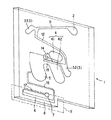
図1は、本発明に係るマイクロチップの構造を説明するための概略図である。
マイクロチップ1は、例えば2枚の板部材を貼り合わせて構成される。貼り合わせ面の片面に予め溝が形成され、貼り合わせることで溝が空洞を形成する。具体的には、各々の板部材の間に、検体溜まり3、試薬溜まり4、混合部5、測定液充填部6を有する。またマイクロチップ1は、一方の面に検体導入部2及び吸引機構接続部7を有し、凸状の検出部8が形成されている。
FIG. 1 is a schematic view for explaining the structure of a microchip according to the present invention.
The
検体導入部2は、例えば血液のような検体を導入させるためのものであり、板部材の一方の面に設けられた孔である。
検体溜まり3は、第1の検体溜まり31と第2の検体溜まり32とからなる。第1の検体溜まり31は、流路11により検体導入部2に通じ、さらに、流路12により第2の検体溜まり32に通じている。
試薬溜まり4は、基質液を充填するための第1の試薬溜まり41と緩衝液を充填するための第2の試薬溜まり42からなる。
混合部5は、基質液、緩衝液及び検体を混合して測定液とするためのものであり、流路13、14及び15により、それぞれ、第2の検体溜まり32、第1の試薬溜まり41及び第2の試薬溜まり42に通じている。
混合部5に充填された測定液は、流路16内で十分に攪拌されて測定液充填部6へ充填される。
吸引機構接続部7は、測定液を吸引することによって測定液充填部6に導くための、図示していない吸引ポンプが接続される箇所であり、排出流路17により測定液充填部6に接続されている。
検出部8は、板部材に形成された凸部分の内部に測定液を充填するための測定液充填部6を有するものであって、例えば放電ランプ等の光源からの光を透過させて吸光光度法によって測定液中に含まれる所望の成分の濃度測定を行うための箇所である。
The
The
The
The
The measurement liquid filled in the
The suction
The
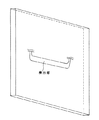
図2は、図1に示すX部分の拡大図である。
検出部8は、板部材に形成された凸部分からなり、方形体形状を有し、その長手方向軸が光軸に略一致している。そして、一方の端面81において凹所82が形成され、この凹所82には光入射面83が形成されている。他方の端面84において凹所85が形成され、この凹所85には光出射面86が形成されている。そして、凹所82と凹所85とは光軸方向において対向している。
FIG. 2 is an enlarged view of a portion X shown in FIG.
The
ここで、板部材の凸部分に検出部を設けることの利点を以下に説明する。検出路の長さ(光路長)は使用する試薬の種類毎に異なり、例えば吸収量の大きい試薬を使用する場合には、光路長を短くする必要がある。そのため、使用する試薬の種類に応じて適当な長さの検出部を有するマイクロチップを選択する必要があるところ、本発明に係るマイクロチップのような構造とすると、試薬の種類に応じて検出部の長さを適宜調整することができる。
その一方で、吸収量の大きい試薬を使用すべく全長の短い検出部を、例えば図3に示すように板部材の中央部付近に設けた構造とした場合には、後述の光源からの光が板部材によって吸収あるいは散乱することにより精度良く吸光度を測定することができない、という問題が生じる。
Here, the advantage of providing a detection part in the convex part of a board member is demonstrated below. The length of the detection path (optical path length) varies depending on the type of reagent to be used. For example, when a reagent having a large absorption amount is used, it is necessary to shorten the optical path length. Therefore, it is necessary to select a microchip having a detection unit having an appropriate length according to the type of reagent to be used. When the microchip according to the present invention is configured, the detection unit is selected according to the type of reagent. Can be adjusted as appropriate.
On the other hand, when a detection unit having a short overall length is used in the vicinity of the center of the plate member as shown in FIG. 3 to use a reagent with a large absorption amount, light from a light source described later is emitted. There is a problem that the absorbance cannot be measured with high accuracy due to absorption or scattering by the plate member.
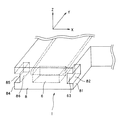
図4は、本発明のマイクロチップ用の吸光度測定ユニットを説明するための概略図である。図4(a)は、マイクロチップ1をチップホルダ10に差し込んだ状態を示す。図4(b)は、図4(a)のA−A´断面図を示す。
FIG. 4 is a schematic diagram for explaining an absorbance measurement unit for a microchip according to the present invention. FIG. 4A shows a state where the
チップホルダ10は、2つ割りの部材からなり、一方の内面に直線状の溝が形成されており、2つの部材を合わせることにより、キャピラリー部11が形成されることになる。このように、2つの部材を合わせることにより、キャピラリー部11をチップホルダ10内に簡便に形成することができる。キャピラリー部11の開口径は、検出部8の光軸に垂直な断面の径より狭い径になっている。一例を挙げると、キャピラリー部11の開口径は0.3mm角、検出部8の光軸に垂直な断面の径は0.7mm角である。かかるキャピラリー部11を設ける必要があるのは、本発明に係るマイクロチップ1が、上記のように、板部材に形成された凸部分に検出部が設けられている、という特殊な構造を有することによる。
The
チップホルダ10には、光入射面83にキャピラリー部11の端部が対向するようにマイクロチップ1が差し込まれる。検出部8内の測定液充填部6を透過した光を検出するためのシリコンフォトダイオードからなる受光素子14が、光出射面86に対向して配置されている。
キャピラリー部11に入射する光は、光源13から放射されてバンドパスフィルタ12で選別された光であり、キャピラリー部11を通過して検出部8に入り、検出部8内の測定液充填部6を透過した後、受光素子14で受光される。キャピラリー部11を通過して検出部8に入射する光は平行光成分が多く、吸光度の測定精度を向上させる。
The
Light incident on the
光源13は、発光管内に発光物質としてキセノンが封入されたキセノンランプである。キセノンランプは、点光源に近く、平行光を効率良く取り出すことが可能な放射特性を有することにより、後述のような微小領域(検出部8)に光源からの光を入射することを要求されるマイクロチップ用の光源として適しており、また、紫外域から可視域においてブロードな光が放射されることにより、分析検体に応じた波長の光を利用することが可能であるため、分析検体毎に光源を交換する必要がない、という利点を有する。さらには、発光物質として水銀を使用しないことから、環境への負荷も小さい。
The
ここで、本発明に係るマイクロチップにおいて、血液中に含まれる酵素の濃度を測定する手順の一例を説明する。以下、一例としてγ−GTPの濃度測定方法について説明する。
〔試薬〕
基質液:GluCANA(L−γ−グルタミル−3−カルボキシ−4−ニトロアニリド) 31mmol/L
緩衝液:グリシルグリシン 193mmol/L pH7.9(30℃)
〔測定手順〕
(1)先端が非常に鋭利な無痛針によって採血した血液を検体導入部2からマイクロチップ1の内部に導入する。
(2)マイクロチップ1に対し6000回転の遠心分離処理を施すことによって分離された血漿が第1の検体溜まり31に満たされる。
(3)再びマイクロチップ1に対し6000回転の遠心分離処理を施すことによって適当な量の血漿が第2の検体溜まり32に満たされる。
(4)マイクロチップ1を反時計回り方向に90°回転させることによって、第2の検体溜まり32に満たされている血漿、第1の試薬溜まり41に満たされている基質液及び第2の試薬溜まり42に満たされている緩衝液を混合部5に流入させて混合を行い測定液とする。血漿に上記の基質液及び緩衝液を作用させると、図5に示すように、血漿中のγ−GTPの作用により、基質L−γ−グルタミル−3−カルボキシ−4−ニトロアニリドのγ−グルタミル基はグリシルグリシンに転移し、測定液中においては、L−γ−グルタミルグリシルグリシンを生成すると同時に、5−アミノ−2−ニトロ安息香酸が遊離する。
(5)測定液充填部6に、測定液を充填させる。充填作業は、吸引ポンプを吸引機構接続部7に接続して、測定液充填部6を負圧にすることによって行われる。
(6)検出部8に光源からの光を透過させて、上記5−アミノ−2−ニトロ安息香酸が吸収を持つ波長405nmの吸収量を検出し、この検出結果に基づいて吸光光度法により5−アミノ−2−ニトロ安息香酸の濃度を求める。そして、5−アミノ−2−ニトロ安息香酸の生成量によって、測定液中のγ−GTPの濃度が求まる。
Here, an example of a procedure for measuring the concentration of an enzyme contained in blood in the microchip according to the present invention will be described. Hereinafter, as an example, a method for measuring the concentration of γ-GTP will be described.
〔reagent〕
Substrate solution: GluCANA (L-γ-glutamyl-3-carboxy-4-nitroanilide) 31 mmol / L
Buffer: glycylglycine 193 mmol / L pH 7.9 (30 ° C.)
〔Measurement procedure〕
(1) Blood sampled by a painless needle having a very sharp tip is introduced from the
(2) The
(3) An appropriate amount of plasma is filled in the
(4) By rotating the
(5) The measurement
(6) The light from the light source is transmitted through the
以上のような本発明のマイクロチップによれば、検出部8において凹所82及び凹所85が形成されていることにより、光入射面等に傷が生じたり不純物が付着したりする、という不具合が生じることを確実に防止することができるため、例えば血液などの測定検体中に含まれる所望の酵素成分の定量値に誤差が生じることなく、正確な分析結果を得ることが期待できる。そして、マイクロチップ1をチップホルダ10にセッティングする際に、光出射面等に傷をつけないようにすべく過剰な神経を使う必要がなく、また、素手で取り扱うことも可能となるため、作業性が向上する。
According to the microchip of the present invention as described above, since the
これに対し、従来のマイクロチップのように検出部に凹所を有しない構造によると、光入射面等に傷が生じたり不純物が付着することにより、定量値に誤差が生じるため正確な分析結果を得ることができないと考えられる。そして、かかる測定誤差が生じることを回避しようとすると、マイクロチップを吸光度測定装置にセッティングする際に、例えばチップホルダのような周辺機器に光入射面等が接触して光入射面等に傷をつけたり、あるいは光入射面等に不純物が付着したりすることを防止すべく過剰な神経を使う必要が生じ、作業性の面で好ましくない。 On the other hand, if the structure does not have a recess in the detection part like a conventional microchip, an error will occur in the quantitative value due to scratches or impurities on the light incident surface, etc. It is thought that can not be obtained. In order to avoid the occurrence of such measurement errors, when the microchip is set in the absorbance measuring device, the light incident surface or the like comes into contact with a peripheral device such as a chip holder, and the light incident surface or the like is damaged. It is necessary to use an excessive amount of nerves to prevent attachment of impurities to the light incident surface or the like, which is not preferable in terms of workability.
以下、本発明の作用効果を確認するために行った実験について説明する。 Hereinafter, experiments conducted for confirming the effects of the present invention will be described.
〔実施例〕
図1に示す構造に従い、本発明に係るマイクロチップ1を作製した。このマイクロチップ1の構成は、以下に示すとおりである。
マイクロチップ1を構成する板部材は、ポリエチレンテレフタラート(PET)からなり、縦(検出部8を含む)が25mm、横が25mmであり、厚みが2mmである。
検出部に係る数値例について図2を参照して詳細に説明する。検出部8は、縦(Y軸)が2.5mm、横(X軸)が12.0mm、厚みが2mmである。第1の凹所82は、深さ(X軸)が1mmである。光入射面83は、縦(Z軸)が1mmであり、横(Y軸)が2mmである。第2の凹所85は、深さ(X軸)が1mmである。光出射面86は、縦(Z軸)が1mmであり、横(Y軸)が2mmである。
測定検体は、1〜2μL(マイクロリットル)の血液である。
試薬は、上記の〔試薬〕に記載したとおりであり、2.1μLのGluCANAを基質液とし、8.4μLのグリシルグリシンを緩衝液として使用した。
〔Example〕
A
The plate member constituting the
A numerical example related to the detection unit will be described in detail with reference to FIG. The
The measurement specimen is 1-2 μL (microliter) of blood.
The reagent was as described in [Reagent] above, and 2.1 μL of GluCANA was used as a substrate solution, and 8.4 μL of glycylglycine was used as a buffer solution.
〔比較例〕
検出部の両端面において凹所を有しないことを除く他の構造は、実施例に係るマイクロチップ1と同様のマイクロチップを作製した。
[Comparative example]
A microchip similar to the
作製した実施例に係るマイクロチップ及び比較例に係るマイクロチップを使用して図4に示す吸光度測定ユニットを構成し、それぞれのユニットに対し、75Wのキセノンランプから放射された光をキャピラリー部を通じて検出部に入射させ、測定液充填部を透過した光を受光素子によって検出し、波長が405nmの光の透過率について調べた。尚、この実験は、前述の測定手順に記載した(1)〜(5)の手順を行わない状態、すなわち、測定液充填部が空の状態で行った。表1にその結果を示す。表1では、比較例1、2、3及び4の光透過率を、実施例に係るマイクロチップの光透過率を100%とする相対値にて示す。 The absorbance measurement unit shown in FIG. 4 is configured using the manufactured microchip according to the example and the microchip according to the comparative example, and the light emitted from the 75 W xenon lamp is detected for each unit through the capillary section. The light transmitted through the measurement liquid filling portion was detected by a light receiving element, and the transmittance of light having a wavelength of 405 nm was examined. In addition, this experiment was performed in the state which does not perform the procedure of (1)-(5) described in the above-mentioned measurement procedure, ie, the measurement liquid filling part is empty. Table 1 shows the results. In Table 1, the light transmittance of Comparative Examples 1, 2, 3, and 4 is shown as a relative value with the light transmittance of the microchip according to the example being 100%.

表1に示すとおり、比較例1及び比較例2に係るマイクロチップは、実施例に係るマイクロチップに比して、その光透過率が低下していることが判明した。これは、比較例1及び比較例2に係るマイクロチップは、その光入射面等に対し、吸光度測定装置へセッティングする際に、例えばチップホルダのような周辺機器と接触したことに起因する傷がついていることが影響している、と推測される。さらに、比較例3及び比較例4に係るマイクロチップは、実施例に係るマイクロチップに比して、その光透過率が増加していることが判明した。これは、比較例3及び比較例4に係るマイクロチップは、検出部の両端面に対して皮脂などの不純物が付着したことにより、検出部の両端面に存在する凹凸(マイクロチップの製造時には多少の凹凸が形成される)が埋まったことによるものと考えられる。
以上から、比較例に係るマイクロチップによると、検出部の光入射面等に生じる傷や付着した皮脂などの不純物に起因して、波長が405nmの光の透過率に誤差が生じるため、正確な分析結果を得ることができず、本発明のように検出部の端部に凹所を有する構造の有効性が確認された。
As shown in Table 1, it was found that the light transmittance of the microchips according to Comparative Example 1 and Comparative Example 2 was lower than that of the microchip according to the example. This is because the microchip according to Comparative Example 1 and Comparative Example 2 has scratches caused by contact with peripheral devices such as a chip holder when setting the light incident surface or the like to the absorbance measuring device. It is speculated that the fact that it is attached has an effect. Furthermore, it was found that the light transmittance of the microchips according to Comparative Example 3 and Comparative Example 4 was increased as compared with the microchip according to the example. This is because the microchips according to Comparative Example 3 and Comparative Example 4 have irregularities present on both end surfaces of the detection unit (somewhat during the manufacture of the microchips) because impurities such as sebum adhere to the both end surfaces of the detection unit. It is thought that this is due to the fact that the irregularities of
From the above, according to the microchip according to the comparative example, an error occurs in the transmittance of light having a wavelength of 405 nm due to impurities such as scratches and attached sebum on the light incident surface of the detection unit. The analysis result could not be obtained, and the effectiveness of the structure having a recess at the end of the detection unit as in the present invention was confirmed.
1 マイクロチップ
2 検体導入部
3 検体溜まり
4 試薬溜まり
5 混合部
6 測定液充填部
7 吸引機構接続部
8 検出部
10 チップホルダ
11 キャピラリー部
12 バンドパスフィルタ
13 光源
14 受光素子
82 凹所
83 光入射面
85 凹所
86 光出射面
DESCRIPTION OF
Claims (1)
前記検出部は、板部材の凸部分によって形成され、その長手方向軸が光軸に対して一致するように配置され、
前記検出部の長手方向における両端面のそれぞれには、前記測定液充填部に光を導入する光入射面を有する凹所と、前記測定液充填部を透過した光を出射する光出射面を有する凹所とが形成されていることを特徴とするマイクロチップ。 A sample introduction part that is made of a plate member, introduces a specimen, a reagent that reacts with the specimen, a mixing part that mixes the reagent and the specimen to generate a measurement liquid, and a measurement liquid filling that fills the measurement liquid In a microchip provided with a detection unit having a part,
The detection unit is formed by a convex portion of a plate member, and is arranged so that its longitudinal axis coincides with the optical axis,
Each of both end surfaces in the longitudinal direction of the detection unit has a recess having a light incident surface for introducing light into the measurement liquid filling unit, and a light emission surface for emitting light transmitted through the measurement liquid filling unit. A microchip, wherein a recess is formed .
Priority Applications (6)
| Application Number | Priority Date | Filing Date | Title |
|---|---|---|---|
| JP2004274673A JP4375183B2 (en) | 2004-09-22 | 2004-09-22 | Microchip |
| TW094121661A TW200610952A (en) | 2004-09-22 | 2005-06-28 | Microchip |
| DE602005016506T DE602005016506D1 (en) | 2004-09-22 | 2005-09-09 | Microchip for absorption spectroscopic analysis |
| EP05019660A EP1640703B1 (en) | 2004-09-22 | 2005-09-09 | Absorption spectrometric analysis microchip |
| US11/224,955 US7981689B2 (en) | 2004-09-22 | 2005-09-14 | Absorption spectrometric analysis microchip and method |
| CNB200510106813XA CN100570332C (en) | 2004-09-22 | 2005-09-22 | Microplate |
Applications Claiming Priority (1)
| Application Number | Priority Date | Filing Date | Title |
|---|---|---|---|
| JP2004274673A JP4375183B2 (en) | 2004-09-22 | 2004-09-22 | Microchip |
Publications (2)
| Publication Number | Publication Date |
|---|---|
| JP2006090774A JP2006090774A (en) | 2006-04-06 |
| JP4375183B2 true JP4375183B2 (en) | 2009-12-02 |
Family
ID=35462319
Family Applications (1)
| Application Number | Title | Priority Date | Filing Date |
|---|---|---|---|
| JP2004274673A Active JP4375183B2 (en) | 2004-09-22 | 2004-09-22 | Microchip |
Country Status (6)
| Country | Link |
|---|---|
| US (1) | US7981689B2 (en) |
| EP (1) | EP1640703B1 (en) |
| JP (1) | JP4375183B2 (en) |
| CN (1) | CN100570332C (en) |
| DE (1) | DE602005016506D1 (en) |
| TW (1) | TW200610952A (en) |
Families Citing this family (23)
| Publication number | Priority date | Publication date | Assignee | Title |
|---|---|---|---|---|
| JP4506375B2 (en) * | 2004-09-22 | 2010-07-21 | ウシオ電機株式会社 | Absorbance measurement unit |
| JP4912096B2 (en) * | 2006-09-07 | 2012-04-04 | ローム株式会社 | Microchip inspection device |
| US20090141282A1 (en) * | 2007-12-04 | 2009-06-04 | Yung-Lieh Chien | Concentration measuring structure capable of reducing the effect of environmental temperature |
| JP5726167B2 (en) * | 2009-04-13 | 2015-05-27 | マイクロニクス, インコーポレイテッド | Microfluidic clinical analyzer |
| CA2786569C (en) | 2010-01-29 | 2019-04-09 | Micronics, Inc. | Sample-to-answer microfluidic cartridge |
| US9182353B2 (en) | 2010-07-22 | 2015-11-10 | Hach Company | Lab-on-a-chip for alkalinity analysis |
| FR2981283B1 (en) * | 2011-10-13 | 2014-08-29 | Chambre De Commerce Et De L Ind De Paris Au Titre De Son Etablissement D Enseignement Superieur Esie | MICROFLUIDIC DEVICE FOR ANALYZING A FLUID UNDER PRESSURE. |
| US8741234B2 (en) * | 2011-12-27 | 2014-06-03 | Honeywell International Inc. | Disposable cartridge for fluid analysis |
| US9180449B2 (en) | 2012-06-12 | 2015-11-10 | Hach Company | Mobile water analysis |
| USD768872S1 (en) | 2012-12-12 | 2016-10-11 | Hach Company | Cuvette for a water analysis instrument |
| JP6498125B2 (en) | 2012-12-21 | 2019-04-10 | マイクロニクス, インコーポレイテッド | Fluid circuit and associated manufacturing method |
| KR20150097764A (en) | 2012-12-21 | 2015-08-26 | 마이크로닉스 인코포레이티드. | Portable fluorescence detection system and microassay cartridge |
| EP3549674B1 (en) | 2012-12-21 | 2020-08-12 | PerkinElmer Health Sciences, Inc. | Low elasticity films for microfluidic use |
| US10386377B2 (en) | 2013-05-07 | 2019-08-20 | Micronics, Inc. | Microfluidic devices and methods for performing serum separation and blood cross-matching |
| EP2994532B1 (en) | 2013-05-07 | 2017-11-15 | Micronics, Inc. | Methods for preparation of nucleic acid-containing samples using clay minerals and alkaline solutions |
| CA2911308C (en) | 2013-05-07 | 2021-10-19 | Micronics, Inc. | Device for preparation and analysis of nucleic acids |
| JP6588910B2 (en) | 2014-06-30 | 2019-10-09 | Phcホールディングス株式会社 | Sample analysis substrate, sample analysis apparatus, sample analysis system, and program for sample analysis system |
| EP3163307B1 (en) | 2014-06-30 | 2021-03-03 | PHC Holdings Corporation | Substrate for sample analysis, sample analysis device, sample analysis system, and method for removing liquid from liquid that contains magnetic particles |
| WO2016002731A1 (en) | 2014-06-30 | 2016-01-07 | パナソニックヘルスケアホールディングス株式会社 | Substrate for sample analysis, and sample analysis apparatus |
| US10309976B2 (en) | 2014-06-30 | 2019-06-04 | Phc Holdings Corporation | Substrate for sample analysis, sample analysis device, sample analysis system, and program for sample analysis system |
| WO2016093332A1 (en) | 2014-12-12 | 2016-06-16 | パナソニックヘルスケアホールディングス株式会社 | Substrate for sample analysis, sample analysis device, sample analysis system, and program for sample analysis system |
| KR20180080396A (en) * | 2017-01-02 | 2018-07-12 | 한국전자통신연구원 | Bio-sensor |
| US20230002801A1 (en) * | 2021-01-12 | 2023-01-05 | Repligen Corporation | Offline and inline determination of concentration of metabolites in cell culture fluid |
Family Cites Families (18)
| Publication number | Priority date | Publication date | Assignee | Title |
|---|---|---|---|---|
| SE399768B (en) * | 1975-09-29 | 1978-02-27 | Lilja Jan E | CYVETT FOR SAMPLING, MIXING OF, THE SAMPLE WITH A REAGENTS AND DIRECT PERFORMANCE OF, SPECIAL OPTICAL, ANALYSIS OF THE SAMPLE MIXED WITH THE REAGENTS |
| US4226531A (en) * | 1977-08-29 | 1980-10-07 | Instrumentation Laboratory Inc. | Disposable multi-cuvette rotor |
| US5798215A (en) * | 1993-02-18 | 1998-08-25 | Biocircuits Corporation | Device for use in analyte detection assays |
| US6046840A (en) * | 1995-06-19 | 2000-04-04 | Reflectivity, Inc. | Double substrate reflective spatial light modulator with self-limiting micro-mechanical elements |
| US6088102A (en) * | 1997-10-31 | 2000-07-11 | Silicon Light Machines | Display apparatus including grating light-valve array and interferometric optical system |
| WO1999060397A1 (en) * | 1998-05-18 | 1999-11-25 | University Of Washington | Liquid analysis cartridge |
| US6188519B1 (en) * | 1999-01-05 | 2001-02-13 | Kenneth Carlisle Johnson | Bigrating light valve |
| AU2099401A (en) * | 1999-12-14 | 2001-06-25 | Combustion Specialists, Inc. | Sensing system for detection and control of deposition on pendant tubes in recovery and power boilers |
| US20020187485A1 (en) * | 2000-10-25 | 2002-12-12 | Jakobsen Mogens Hausteen | Open substrate platforms suitable for analysis of biomolecules |
| JP3760810B2 (en) * | 2001-07-06 | 2006-03-29 | ソニー株式会社 | Light modulation element, GLV device, and laser display |
| JP2003279471A (en) | 2002-03-20 | 2003-10-02 | Nippon Sheet Glass Co Ltd | Chip for microchemical system and microchemical system |
| US6768555B2 (en) * | 2002-03-21 | 2004-07-27 | Industrial Technology Research Institute | Fabry-Perot filter apparatus with enhanced optical discrimination |
| JP2004077305A (en) * | 2002-08-19 | 2004-03-11 | Nec Corp | Detector |
| JP2004109099A (en) * | 2002-09-16 | 2004-04-08 | Jun Kikuchi | Method of analyzing blood, apparatus for analyzing blood, and method of manufacturing apparatus for analyzing blood |
| JP4057871B2 (en) * | 2002-09-19 | 2008-03-05 | 東芝松下ディスプレイテクノロジー株式会社 | Liquid crystal display |
| US6822780B1 (en) * | 2003-06-23 | 2004-11-23 | Northrop Grumman Corporation | Vertically stacked spatial light modulator with multi-bit phase resolution |
| WO2005033666A1 (en) * | 2003-10-03 | 2005-04-14 | National Institute For Materials Science | Chip using method and test chip |
| US7710632B2 (en) * | 2004-09-27 | 2010-05-04 | Qualcomm Mems Technologies, Inc. | Display device having an array of spatial light modulators with integrated color filters |
-
2004
- 2004-09-22 JP JP2004274673A patent/JP4375183B2/en active Active
-
2005
- 2005-06-28 TW TW094121661A patent/TW200610952A/en not_active IP Right Cessation
- 2005-09-09 DE DE602005016506T patent/DE602005016506D1/en active Active
- 2005-09-09 EP EP05019660A patent/EP1640703B1/en not_active Expired - Fee Related
- 2005-09-14 US US11/224,955 patent/US7981689B2/en active Active
- 2005-09-22 CN CNB200510106813XA patent/CN100570332C/en not_active Expired - Fee Related
Also Published As
| Publication number | Publication date |
|---|---|
| TW200610952A (en) | 2006-04-01 |
| TWI343994B (en) | 2011-06-21 |
| CN100570332C (en) | 2009-12-16 |
| EP1640703A2 (en) | 2006-03-29 |
| US20060061760A1 (en) | 2006-03-23 |
| CN1752741A (en) | 2006-03-29 |
| DE602005016506D1 (en) | 2009-10-22 |
| JP2006090774A (en) | 2006-04-06 |
| EP1640703B1 (en) | 2009-09-09 |
| US7981689B2 (en) | 2011-07-19 |
| EP1640703A3 (en) | 2006-06-07 |
Similar Documents
| Publication | Publication Date | Title |
|---|---|---|
| JP4375183B2 (en) | Microchip | |
| EP2745779B1 (en) | Capillary microcuvette having double collection means | |
| JP4627395B2 (en) | Analytical cartridge and liquid feeding control device | |
| US8143077B2 (en) | Microchip and method of manufacturing microchip | |
| JP4111179B2 (en) | Chemical analyzer and chemical analysis system | |
| JP2007501415A (en) | Apparatus and method for process monitoring | |
| JP2009128229A (en) | Microchip | |
| JP2009109196A (en) | Dilution ratio deriving method, quantity determination method and analyzer | |
| WO2008053743A1 (en) | Microchip and analyzer using the same | |
| EP3112847A1 (en) | Measurement method and measurement device | |
| JP5802499B2 (en) | Analysis equipment | |
| WO2005047868A1 (en) | Fluorescence measuring device | |
| JP5254751B2 (en) | Microchip | |
| US10114032B2 (en) | Blood coagulation test method | |
| JP2009121912A (en) | Microchip | |
| US7569183B2 (en) | Fecal assay method and analyzer | |
| JP2008058127A (en) | Autoanalyzer | |
| JP4969923B2 (en) | Sample measurement method | |
| US20190175154A1 (en) | Apparatus for Drawing of a Bodily Fluid and Method Therefor | |
| KR102458032B1 (en) | Rt-pcr device | |
| JP5758949B2 (en) | Blood coagulation test method | |
| JP5017723B2 (en) | Microchip having optical measurement cuvette and method of using the same | |
| CN114206743A (en) | Reagent kit | |
| JP2009085818A (en) | Liquid reagent built-in type microchip | |
| CN104777293A (en) | Detection device and detection method |
Legal Events
| Date | Code | Title | Description |
|---|---|---|---|
| A621 | Written request for application examination |
Free format text: JAPANESE INTERMEDIATE CODE: A621 Effective date: 20070306 |
|
| RD04 | Notification of resignation of power of attorney |
Free format text: JAPANESE INTERMEDIATE CODE: A7424 Effective date: 20090119 |
|
| A977 | Report on retrieval |
Free format text: JAPANESE INTERMEDIATE CODE: A971007 Effective date: 20090520 |
|
| A131 | Notification of reasons for refusal |
Free format text: JAPANESE INTERMEDIATE CODE: A131 Effective date: 20090602 |
|
| A521 | Request for written amendment filed |
Free format text: JAPANESE INTERMEDIATE CODE: A523 Effective date: 20090717 |
|
| TRDD | Decision of grant or rejection written | ||
| A01 | Written decision to grant a patent or to grant a registration (utility model) |
Free format text: JAPANESE INTERMEDIATE CODE: A01 Effective date: 20090818 |
|
| A01 | Written decision to grant a patent or to grant a registration (utility model) |
Free format text: JAPANESE INTERMEDIATE CODE: A01 |
|
| A61 | First payment of annual fees (during grant procedure) |
Free format text: JAPANESE INTERMEDIATE CODE: A61 Effective date: 20090831 |
|
| R150 | Certificate of patent or registration of utility model |
Ref document number: 4375183 Country of ref document: JP Free format text: JAPANESE INTERMEDIATE CODE: R150 Free format text: JAPANESE INTERMEDIATE CODE: R150 |
|
| FPAY | Renewal fee payment (event date is renewal date of database) |
Free format text: PAYMENT UNTIL: 20120918 Year of fee payment: 3 |
|
| S111 | Request for change of ownership or part of ownership |
Free format text: JAPANESE INTERMEDIATE CODE: R313113 |
|
| FPAY | Renewal fee payment (event date is renewal date of database) |
Free format text: PAYMENT UNTIL: 20120918 Year of fee payment: 3 |
|
| R350 | Written notification of registration of transfer |
Free format text: JAPANESE INTERMEDIATE CODE: R350 |
|
| FPAY | Renewal fee payment (event date is renewal date of database) |
Free format text: PAYMENT UNTIL: 20120918 Year of fee payment: 3 |
|
| FPAY | Renewal fee payment (event date is renewal date of database) |
Free format text: PAYMENT UNTIL: 20130918 Year of fee payment: 4 |
|
| S111 | Request for change of ownership or part of ownership |
Free format text: JAPANESE INTERMEDIATE CODE: R313113 |
|
| R350 | Written notification of registration of transfer |
Free format text: JAPANESE INTERMEDIATE CODE: R350 |
|
| R250 | Receipt of annual fees |
Free format text: JAPANESE INTERMEDIATE CODE: R250 |
|
| R250 | Receipt of annual fees |
Free format text: JAPANESE INTERMEDIATE CODE: R250 |
|
| R250 | Receipt of annual fees |
Free format text: JAPANESE INTERMEDIATE CODE: R250 |
|
| R250 | Receipt of annual fees |
Free format text: JAPANESE INTERMEDIATE CODE: R250 |
|
| R250 | Receipt of annual fees |
Free format text: JAPANESE INTERMEDIATE CODE: R250 |