JP4368535B2 - Measuring chip - Google Patents
Measuring chip Download PDFInfo
- Publication number
- JP4368535B2 JP4368535B2 JP2001092666A JP2001092666A JP4368535B2 JP 4368535 B2 JP4368535 B2 JP 4368535B2 JP 2001092666 A JP2001092666 A JP 2001092666A JP 2001092666 A JP2001092666 A JP 2001092666A JP 4368535 B2 JP4368535 B2 JP 4368535B2
- Authority
- JP
- Japan
- Prior art keywords
- dielectric block
- sample
- light beam
- block
- thin film
- Prior art date
- Legal status (The legal status is an assumption and is not a legal conclusion. Google has not performed a legal analysis and makes no representation as to the accuracy of the status listed.)
- Expired - Fee Related
Links
- 238000005259 measurement Methods 0.000 claims description 101
- 238000002198 surface plasmon resonance spectroscopy Methods 0.000 claims description 69
- 229910052751 metal Inorganic materials 0.000 claims description 50
- 239000002184 metal Substances 0.000 claims description 50
- 239000010408 film Substances 0.000 claims description 46
- 230000003287 optical effect Effects 0.000 claims description 37
- 239000010409 thin film Substances 0.000 claims description 37
- 239000000126 substance Substances 0.000 claims description 16
- 239000011347 resin Substances 0.000 claims description 14
- 229920005989 resin Polymers 0.000 claims description 14
- 238000005253 cladding Methods 0.000 claims description 13
- 238000001514 detection method Methods 0.000 claims description 11
- 239000011521 glass Substances 0.000 claims description 4
- 230000005284 excitation Effects 0.000 claims description 3
- 238000009739 binding Methods 0.000 claims description 2
- 239000007788 liquid Substances 0.000 description 12
- 230000000694 effects Effects 0.000 description 8
- 238000007740 vapor deposition Methods 0.000 description 8
- 239000000463 material Substances 0.000 description 6
- 230000002950 deficient Effects 0.000 description 5
- 230000002411 adverse Effects 0.000 description 4
- 238000004458 analytical method Methods 0.000 description 4
- 230000007423 decrease Effects 0.000 description 4
- PCHJSUWPFVWCPO-UHFFFAOYSA-N gold Chemical compound [Au] PCHJSUWPFVWCPO-UHFFFAOYSA-N 0.000 description 3
- 229910052737 gold Inorganic materials 0.000 description 3
- 239000010931 gold Substances 0.000 description 3
- 238000001746 injection moulding Methods 0.000 description 3
- 238000000465 moulding Methods 0.000 description 3
- 230000002093 peripheral effect Effects 0.000 description 3
- 229920003229 poly(methyl methacrylate) Polymers 0.000 description 3
- 239000004926 polymethyl methacrylate Substances 0.000 description 3
- 230000010287 polarization Effects 0.000 description 2
- RYGMFSIKBFXOCR-UHFFFAOYSA-N Copper Chemical compound [Cu] RYGMFSIKBFXOCR-UHFFFAOYSA-N 0.000 description 1
- BQCADISMDOOEFD-UHFFFAOYSA-N Silver Chemical compound [Ag] BQCADISMDOOEFD-UHFFFAOYSA-N 0.000 description 1
- 229910052782 aluminium Inorganic materials 0.000 description 1
- XAGFODPZIPBFFR-UHFFFAOYSA-N aluminium Chemical compound [Al] XAGFODPZIPBFFR-UHFFFAOYSA-N 0.000 description 1
- 239000000427 antigen Substances 0.000 description 1
- 102000036639 antigens Human genes 0.000 description 1
- 108091007433 antigens Proteins 0.000 description 1
- 238000011088 calibration curve Methods 0.000 description 1
- 229910052802 copper Inorganic materials 0.000 description 1
- 239000010949 copper Substances 0.000 description 1
- 150000001925 cycloalkenes Chemical class 0.000 description 1
- 239000003989 dielectric material Substances 0.000 description 1
- 230000005684 electric field Effects 0.000 description 1
- 230000001747 exhibiting effect Effects 0.000 description 1
- 239000003574 free electron Substances 0.000 description 1
- 239000007924 injection Substances 0.000 description 1
- 238000002347 injection Methods 0.000 description 1
- 238000000034 method Methods 0.000 description 1
- 239000005304 optical glass Substances 0.000 description 1
- 239000004417 polycarbonate Substances 0.000 description 1
- 229920000515 polycarbonate Polymers 0.000 description 1
- 229920000098 polyolefin Polymers 0.000 description 1
- 230000000644 propagated effect Effects 0.000 description 1
- 239000004065 semiconductor Substances 0.000 description 1
- 229910052709 silver Inorganic materials 0.000 description 1
- 239000004332 silver Substances 0.000 description 1
- 238000004611 spectroscopical analysis Methods 0.000 description 1
- 229920003002 synthetic resin Polymers 0.000 description 1
- 239000000057 synthetic resin Substances 0.000 description 1
Images


Classifications
-
- G—PHYSICS
- G01—MEASURING; TESTING
- G01N—INVESTIGATING OR ANALYSING MATERIALS BY DETERMINING THEIR CHEMICAL OR PHYSICAL PROPERTIES
- G01N21/00—Investigating or analysing materials by the use of optical means, i.e. using sub-millimetre waves, infrared, visible or ultraviolet light
- G01N21/17—Systems in which incident light is modified in accordance with the properties of the material investigated
- G01N21/55—Specular reflectivity
- G01N21/552—Attenuated total reflection
- G01N21/553—Attenuated total reflection and using surface plasmons
-
- G—PHYSICS
- G01—MEASURING; TESTING
- G01N—INVESTIGATING OR ANALYSING MATERIALS BY DETERMINING THEIR CHEMICAL OR PHYSICAL PROPERTIES
- G01N2201/00—Features of devices classified in G01N21/00
- G01N2201/04—Batch operation; multisample devices
- G01N2201/0415—Carrusel, sequential
Landscapes
- Physics & Mathematics (AREA)
- Health & Medical Sciences (AREA)
- Life Sciences & Earth Sciences (AREA)
- Chemical & Material Sciences (AREA)
- Analytical Chemistry (AREA)
- Biochemistry (AREA)
- General Health & Medical Sciences (AREA)
- General Physics & Mathematics (AREA)
- Immunology (AREA)
- Pathology (AREA)
- Investigating Or Analysing Materials By Optical Means (AREA)
- Optical Measuring Cells (AREA)
- Automatic Analysis And Handling Materials Therefor (AREA)
Description
【0001】
【発明の属する技術分野】
本発明は、表面プラズモンの発生を利用して試料中の物質を定量分析する表面プラズモン共鳴測定装置等に用いられる測定チップに関するものである。
【0002】
【従来の技術】
金属中においては、自由電子が集団的に振動して、プラズマ波と呼ばれる粗密波が生じる。そして、金属表面に生じるこの粗密波を量子化したものは、表面プラズモンと呼ばれている。
【0003】
従来より、この表面プラズモンが光波によって励起される現象を利用して、試料中の物質を定量分析する表面プラズモン共鳴測定装置が種々提案されている。そして、それらの中で特に良く知られているものとして、 Kretschmann配置と称される系を用いるものが挙げられる(例えば特開平6−167443号参照)。
【0004】
上記の系を用いる表面プラズモン共鳴測定装置は基本的に、例えばプリズム状に形成された誘電体ブロックと、この誘電体ブロックの一面に形成されて試料に接触させられる金属膜と、光ビームを発生させる光源と、上記光ビームを誘電体ブロックに対して、該誘電体ブロックと金属膜との界面で全反射条件となり、かつ、表面プラズモン共鳴条件を含む種々の入射角が得られるように入射させる光学系と、上記界面で全反射した光ビームの強度を測定して表面プラズモン共鳴の状態を検出する光検出手段とを備えてなるものである。
【0005】
なお上述のように種々の入射角を得るためには、比較的細い光ビームを偏向させて上記界面に入射させてもよいし、あるいは光ビームに種々の角度で入射する成分が含まれるように、比較的太い光ビームを上記界面に収束光あるいは発散光の状態で入射させてもよい。前者の場合は、光ビームの偏向にともなって反射角が変化する光ビームを、光ビームの偏向に同期移動する小さな光検出器によって検出したり、反射角の変化方向に沿って延びるエリアセンサによって検出することができる。一方後者の場合は、種々の反射角で反射した各光ビームを全て受光できる方向に延びるエリアセンサによって検出することができる。
【0006】
上記構成の表面プラズモン共鳴測定装置において、光ビームを金属膜に対して全反射角以上の特定入射角θSPで入射させると、該金属膜に接している試料中に電界分布をもつエバネッセント波が生じ、このエバネッセント波によって金属膜と試料との界面に表面プラズモンが励起される。エバネッセント光の波数ベクトルが表面プラズモンの波数と等しくて波数整合が成立しているとき、両者は共鳴状態となり、光のエネルギーが表面プラズモンに移行するので、誘電体ブロックと金属膜との界面で全反射した光の強度が鋭く低下する。この光強度の低下は、一般に上記光検出手段により暗線として検出される。
【0007】
なお上記の共鳴は、入射ビームがp偏光のときにだけ生じる。したがって、光ビームがp偏光で入射するように予め設定しておく必要がある。
【0008】
この全反射減衰(ATR)が生じる入射角θSPより表面プラズモンの波数が分かると、試料の誘電率が求められる。すなわち表面プラズモンの波数をKSP、表面プラズモンの角周波数をω、cを真空中の光速、εm とεs をそれぞれ金属、試料の誘電率とすると、以下の関係がある。
【0009】
【数1】

【0010】
上記の系を用いる従来の表面プラズモン共鳴測定装置において、実用上は、試料に接触させる金属膜を測定毎に交換する必要がある。そこで従来は、この金属膜を平坦な板状の誘電体ブロックに固定し、それとは別に前記全反射を生じさせるための光カップラーとしてのプリズム状誘電体ブロックを設け、この後者の誘電体ブロックの一面に前者の誘電体ブロックを一体化するという手法が採用されていた。そのようにすれば、後者の誘電体ブロックは光学系に対して固定としておき、前者の誘電体ブロックと金属膜とを測定チップとして、この測定チップのみを試料毎に交換することが可能となる。
【0011】
また、全反射減衰(ATR)を利用する類似の測定装置として、例えば「分光研究」第47巻 第1号(1998)の第21〜23頁および第26〜27頁に記載がある漏洩モードセンサーも知られている。この漏洩モードセンサーは基本的に、例えばプリズム状に形成された誘電体ブロックと、この誘電体ブロックの一面に形成されたクラッド層と、このクラッド層の上に形成されて、試料に接触させられる光導波層と、光ビームを発生させる光源と、上記光ビームを上記誘電体ブロックに対して、該誘電体ブロックとクラッド層との界面で全反射条件が得られるように種々の角度で入射させる光学系と、上記界面で全反射した光ビームの強度を測定して導波モードの励起状態、つまり全反射減衰状態を検出する光検出手段とを備えてなるものである。
【0012】
上記構成の漏洩モードセンサーにおいて、光ビームを誘電体ブロックを通してクラッド層に対して全反射角以上の入射角で入射させると、このクラッド層を透過した後に光導波層においては、ある特定の波数を有する特定入射角の光のみが導波モードで伝搬するようになる。こうして導波モードが励起されると、入射光のほとんどが光導波層に取り込まれるので、上記界面で全反射する光の強度が鋭く低下する全反射減衰が生じる。そして導波光の波数は光導波層の上の試料の屈折率に依存するので、全反射減衰が生じる上記特定入射角を知ることによって、試料の屈折率や、それに関連する試料の特性を分析することができる。
【0013】
なおこの漏洩モードセンサーを用いる場合も、前述の表面プラズモン共鳴測定装置を用いる場合と同様に、装置の光学系に対して1つの誘電体ブロックを固定する一方、別の誘電体ブロックにクラッド層および光導波層を形成して測定チップとし、この測定チップのみを試料毎に交換することが可能である。
【0014】
【発明が解決しようとする課題】
しかし、この交換可能とされた従来の測定チップを用いる場合は、その誘電体ブロックとプリズム状誘電体ブロックとの間に空隙が生じて屈折率が不連続となることを防止するため、それら両誘電体ブロックを屈折率マッチング液を介して一体化する必要が生じる。そのようにして両誘電体ブロックを一体化する作業は非常に煩雑であり、そのため、この従来の測定チップは、測定に際しての取扱い性が良くないものとなっている。特に、測定チップをターレット等の上に自動装填し、このターレットを回転させることにより、測定チップを光ビームを受ける測定位置に自動供給して測定を自動化するような場合は、測定チップの装填、取外しに手間取り、それが自動測定の能率向上を妨げる原因となりやすい。
【0015】
またこの従来の測定チップは、屈折率マッチング液を使用することから、環境に与える悪影響も懸念されている。
【0016】
本発明は上記の事情に鑑みてなされたものであり、屈折率マッチング液を使用する必要がなく、そして測定用光学系に対して簡単に交換することができる測定チップを提供することを目的とする。
【0017】
【課題を解決するための手段】
本発明による1つの測定チップは、
前述したような誘電体ブロックと、
この誘電体ブロックの一面に形成されて試料に接触させられる薄膜層と、
光ビームを発生させる光源と、
前記光ビームを前記誘電体ブロックに対して、該誘電体ブロックと前記薄膜層との界面で全反射条件となり、かつ、種々の入射角成分を含むようにして入射させる光学系と、
前記界面で全反射した光ビームの強度を測定して全反射減衰の状態を検出する光検出手段とを備えてなる、全反射減衰を利用した測定装置に用いられる測定チップであって、
前記誘電体ブロックが、前記光ビームの入射面、出射面および前記薄膜層が形成される一面の全て、並びに前記薄膜層の上に試料を保持する試料保持機構を含んで一体成形された1つのブロックとして形成され、
この誘電体ブロックに前記薄膜層が一体化されてなることを特徴とするものである。
【0018】
また本発明による別の測定チップは、特に前述の表面プラズモン共鳴測定装置を対象として構成されたものであり、
誘電体ブロックと、
この誘電体ブロックの一面に形成されて試料に接触させられる金属膜からなる薄膜層と、
光ビームを発生させる光源と、
前記光ビームを前記誘電体ブロックに対して、該誘電体ブロックと前記金属膜との界面で全反射条件となり、かつ、種々の入射角成分を含むようにして入射させる光学系と、
前記界面で全反射した光ビームの強度を測定して、表面プラズモン共鳴による全反射減衰の状態を検出する光検出手段とを備えてなる表面プラズモン共鳴測定装置に用いられる測定チップにおいて、
前記誘電体ブロックが、前記光ビームの入射面、出射面および前記金属膜が形成される一面の全て、並びに前記薄膜層の上に試料を保持する試料保持機構を含んで一体成形された1つのブロックとして形成され、
この誘電体ブロックに前記金属膜が一体化されてなることを特徴とするものである。
【0019】
また本発明によるさらに別の測定チップは、特に前述の漏洩モードセンサーを対象として構成されたものであり、
誘電体ブロックと、
この誘電体ブロックの一面に形成されたクラッド層、およびその上に形成されて試料に接触させられる光導波層からなる薄膜層と、
光ビームを発生させる光源と、
前記光ビームを前記誘電体ブロックに対して、該誘電体ブロックと前記クラッド層との界面で全反射条件となり、かつ、種々の入射角成分を含むようにして入射させる光学系と、
前記界面で全反射した光ビームの強度を測定して、前記光導波層での導波モードの励起による全反射減衰の状態を検出する光検出手段とを備えてなる漏洩モードセンサーに用いられる測定チップにおいて、
前記誘電体ブロックが、前記光ビームの入射面、出射面および前記クラッド層が形成される一面の全て、並びに前記薄膜層の上に試料を保持する試料保持機構を含んで一体成形された1つのブロックとして形成され、
この誘電体ブロックに前記クラッド層および光導波層が一体化されてなることを特徴とするものである。
【0020】
なお上記試料保持機構として具体的には、前記薄膜層の上側において側方が閉じられた空間を画成する部材からなり、この部材の内面が、薄膜層から上方に離れるのにつれて側外方に離れる形状とされているものを好適に用いることができる。この形状を採用する場合、薄膜層の上側において側方が閉じられた空間を画成する部材の内面と、誘電体ブロックの薄膜層が形成される一面とは、滑らかな曲面を介して連続していることが望ましい。
【0021】
また本発明による測定チップにおいて、上記誘電体ブロックは、ブロックの上下方向(使用状態に配した場合の上下方向。以下、同様)に垂直な面内の断面外形形状が四角形等の多角形となる形とされるのが望ましい。
【0022】
そして、誘電体ブロックにそのような多角形の外形を採用する場合は、誘電体ブロックの上下方向に垂直な少なくとも一つの面内で、その多角形の隅部が丸みを帯びた形状となっていることが望ましい。なお、このように「多角形の隅部が丸みを帯びた」形状として具体的には、誘電体ブロックの隣接する2つの側面どうしが共有する端縁の部分が丸みを帯びた形状と、誘電体ブロックの隣接する2つの側面と底面とが共有する隅部が丸みを帯びた形状とがあり、勿論、それら双方の形状が併せて採用されてもよい。
【0023】
また上述のような多角形の外形を採用する場合、誘電体ブロックは、その多角形が上方に向かって次第に大きくなるテーパ状の外形部分を備えていることが望ましい。そして、そのように多角形とテーパ状の外形を採用する場合、テーパ状の外形部分をなすブロック側面の、ブロック上下方向軸に対する角度は3〜15°の範囲にあることが望ましい。
【0024】
他方、上記誘電体ブロックを形成するのに好適な材料としては、例えばガラスや透明樹脂を挙げることができる。透明樹脂を用いる場合は、上記試料保持機構も該誘電体ブロックと一体的に成形するのが望ましい。
【0025】
一方前記薄膜層の上には、試料中の特定物質と結合反応を示すセンシング媒体が固定されていることが望ましい。
【0026】
【発明の効果】
本発明による測定チップは、誘電体ブロックが、光ビームの入射面、出射面および薄膜層が形成される一面の全てを含む1つのブロック(これは、上述の通り光ビームの入射面および出射面を備えているので、光カップラーとしても機能するものである)として形成され、この誘電体ブロックに薄膜層が一体化されてなるので、この測定チップ全体を光学系に対して装脱するだけで簡単に交換可能となる。
【0027】
つまり、従来技術におけるように、光学系に対して固定した光カップラー単体としての誘電体ブロックに別の誘電体ブロックを一体化する構成ではないので、両誘電体ブロックを屈折率マッチング液を介して一体化する必要がなく、この屈折率マッチング液を用いることによる取扱い性の悪さを解消することができる。
【0028】
また、屈折率マッチング液を用いる必要が無ければ、それが環境に悪影響を与えることも防止される。
【0029】
一方、特に前述した薄膜層の上に試料を保持する試料保持機構が設けられ、この試料保持機構が、薄膜層の上側において側方が閉じられた空間を画成する部材からなり、この部材の内面が、薄膜層から上方に離れるのにつれて側外方に離れる形状とされている場合は、薄膜層の厚みを均一化する効果を得ることもできる。すなわち、金属膜等からなるこの薄膜層は一般に蒸着によって形成されるので、その場合に試料保持機構を上述のような形状としておけば、蒸着に際して蒸着材料が試料保持機構に遮られて薄膜層の厚みが不均一になることを防止可能である。
【0030】
そして、上記空間を画成する部材の内面に上述の形状を採用する場合、特にこの部材の内面と、誘電体ブロックの薄膜層が形成される一面とが滑らかな曲面を介して連続しているものにあっては、それらを樹脂を用いて一体的に射出成形する際に、成形型からの抜けが良くなるので、不良品の発生が少なく抑えられるようになる。
【0031】
一方誘電体ブロックが、その上下方向に垂直な面内の断面外形形状が多角形となる形とされた場合においても、その多角形の隅部が丸みを帯びた形状とされていれば、それを樹脂を用いて一体的に射出成形する際に、成形型からの抜けが良くなるので、不良品の発生が少なく抑えられるようになる。
【0032】
また本発明の測定チップにおいて、上記誘電体ブロックが、ブロックの上下方向に垂直な面内の断面形状が四角形等の多角形で、かつこの多角形が上方に向かって次第に大きくなるテーパ状の外形部分を備えている場合は、このチップを測定装置にセットする際の位置決めが容易化される。
【0033】
すなわち、測定装置側の水平な測定台等に四角形等の多角形の孔を形成して、上記テーパ状の外形部分をそこに上から挿し込み、嵌合させてチップをセットするように構成すれば、多角形部分どうしの嵌合であることから、誘電体ブロックがその上下方向に垂直な面内で(つまり水平面内で)自ずと所定の向きにセットされ、そこから動いてしまうことも無くなる。
【0034】
また、上記テーパ状の外形部分を、測定台等に形成された多角形の孔に上から挿し込めば、誘電体ブロックは上述の多角形部分どうしの嵌合がなされる高さ位置で自ずと止まって保持されるから、チップの高さ方向の位置決めも容易になされ得る。
【0035】
本発明者の研究によると、上述のように誘電体ブロックのテーパ状の外形部分を利用して位置決めを行なう場合、ブロック側面のブロック上下方向軸に対する角度が3〜15°の範囲にあると、位置決め精度が特に高くなることが判明した。その理由は、後に発明の実施の形態に即して詳しく説明する。
【0036】
【発明の実施の形態】
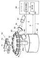
以下、図面を参照して本発明の実施の形態を詳細に説明する。図1は、本発明の第1の実施形態による表面プラズモン共鳴測定チップ(以下、単に測定チップという)10を用いる表面プラズモン共鳴測定装置の全体形状を示すものである。また図2はこの装置の要部の側面形状を示し、図3は測定チップ10の斜視形状を示している。
【0037】
図1に示す通りこの表面プラズモン共鳴測定装置は、複数の測定チップ10を支持するターンテーブル20と、測定用の光ビーム(レーザビーム)30を発生させる半導体レーザ等のレーザ光源31と、入射光学系を構成する集光レンズ32と、光検出器40と、上記ターンテーブル20を間欠的に回動させる支持体駆動手段50と、この支持体駆動手段50の駆動を制御するとともに、上記光検出器40の出力信号Sを受けて後述の処理を行なうコントローラ60と、試料自動供給機構70とを有している。
【0038】
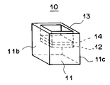
上記測定チップ10は図2および図3に示す通り、例えば直方体状に形成された透明誘電体ブロック11と、この誘電体ブロック11の上面に形成された例えば金、銀、銅、アルミニウム等からなる金属膜12と、この金属膜12の上に側方が閉じられた空間を画成する筒状部材からなる試料保持枠13とから構成されている。誘電体ブロック11は、上記金属膜12が形成される面(後述の界面11aを構成する面)と、光ビーム30が入射する面11bと、光ビーム30が出射する面11cとを全てを含む1つのブロックとして形成されている。試料保持枠13の中には、後述のようにして例えば液体の試料15が貯えられる。
【0039】
測定チップ10は、誘電体ブロック11と試料保持枠13とを例えば透明樹脂等から一体成形してなるものであり、ターンテーブル20に対して交換可能とされている。交換可能とするためには、例えばターンテーブル20に形成された貫通孔に、測定チップ10を嵌合保持させる等すればよい。なお本例では、金属膜12の上にセンシング媒体14が固定されているが、それについては後に詳述する。
【0040】
上記透明樹脂の好ましいものとしては、PMMA、ポリカーボネート、非晶性ポリオレフィン、シクロオレフィン等を挙げることができる。その他に、誘電体ブロック11と試料保持枠13とを一体成形する材料として、ガラスも好適である。また誘電体ブロック11を形成する材料として一般には、屈折率が1.45〜2.5程度の範囲内にあるものを用いるのが望ましい。その理由は、この屈折率範囲で実用的なSPR共鳴角が得られるからである。
【0041】
ターンテーブル20は複数(本例では11個)の上記測定チップ10を、その回動軸20aを中心とする円周上に等角度間隔で支持するように構成されている。支持体駆動手段50はステッピングモータ等から構成され、ターンテーブル20を測定チップ10の配置角度と等しい角度ずつ間欠的に回動させる。
【0042】
集光レンズ32は図2に示す通り、光ビーム30を集光して収束光状態で誘電体ブロック11に通し、誘電体ブロック11と金属膜12との界面11aに対して種々の入射角が得られるように入射させる。この入射角の範囲は、上記界面11aにおいて光ビーム30の全反射条件が得られ、かつ、表面プラズモン共鳴が生じ得る角度範囲を含む範囲とされる。
【0043】
なお光ビーム30は、界面11aに対してp偏光で入射する。そのようにするためには、予めレーザ光源31をその偏光方向が所定方向となるように配設すればよい。その他、波長板や偏光板で光ビーム30の偏光の向きを制御してもよい。
【0044】
光検出器40は、多数の受光素子が1列に配されてなるラインセンサーから構成されており、受光素子の並び方向が図2中の矢印X方向となるように配されている。
【0045】
一方コントローラ60は、支持体駆動手段50からその回動停止位置を示すアドレス信号Aを受けるとともに、所定のシーケンスに基づいてこの支持体駆動手段50を作動させる駆動信号Dを出力する。またこのコントローラ60は、上記光検出器40の出力信号Sを受ける信号処理部61と、この信号処理部61からの出力を受ける表示部62とを備えている。
【0046】
試料自動供給機構70は、例えば液体試料を所定量だけ吸引保持するピペット71と、このピペット71を移動させる手段72とから構成されたものであり、所定位置にセットされた試料容器73から試料をピペット71に吸引保持し、所定の停止位置にある測定チップ10の試料保持枠13内にその試料を滴下供給する。
【0047】
以下、上記構成の表面プラズモン共鳴測定装置による試料分析について説明する。試料分析に際してターンテーブル20は、前述のように支持体駆動手段50によって間欠的に回動される。そして、ターンテーブル20が停止したとき所定位置に静止した測定チップ10の試料保持枠13に、上記試料自動供給機構70によって試料15が供給される。
【0048】
その後ターンテーブル20が何回か回動されてから停止すると、試料保持枠13に試料15を保持している測定チップ10が、その誘電体ブロック11に前記光ビーム30が入射する測定位置(図2中の右側の測定チップ10の位置)に静止する状態となる。この状態のとき、コントローラ60からの指令でレーザ光源31が駆動され、そこから発せられた光ビーム30が前述のように収束する状態で、誘電体ブロック11と金属膜12との界面11aに入射する。この界面11aで全反射した光ビーム30は、光検出器40によって検出される。
【0049】
光ビーム30は、上述の通り収束光状態で誘電体ブロック11に入射するので、上記界面11aに対して種々の入射角θで入射する成分を含むことになる。なおこの入射角θは、全反射角以上の角度とされる。そこで、光ビーム30は界面11aで全反射し、この反射した光ビーム30には、種々の反射角で反射する成分が含まれることになる。ここで、上記集光レンズ32等の光学系は、光ビーム30を界面11aにデフォーカス状態で入射させるように構成されてもよい。そのようにすれば、表面プラズモン共鳴の状態検出(例えば前記暗線の位置測定)の誤差が平均化されて、測定精度が高められる。
【0050】
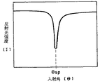
上述のように光ビーム30が全反射するとき、界面11aから金属膜12側にエバネッセント波がしみ出す。そして、光ビーム30が界面11aに対してある特定の入射角θSPで入射した場合は、このエバネッセント波が金属膜12の表面に励起する表面プラズモンと共鳴するので、この光については反射光強度Iが鋭く低下する。なお図4には、この全反射減衰現象が生じた際の入射角θと反射光強度Iとの関係を概略的に示してある。
【0051】
そこで、光検出器40が出力する光量検出信号Sから各受光素子毎の検出光量を調べ、暗線を検出した受光素子の位置に基づいて上記入射角(全反射減衰角)θSPを求め、予め求めておいた反射光強度Iと入射角θとの関係曲線に基づけば、試料15中の特定物質を定量分析することができる。コントローラ60の信号処理部61は、以上の原理に基づいて試料15中の特定物質を定量分析し、その分析結果が表示部62に表示される。
【0052】
測定を1つの試料15に対して1回だけ行なう場合は、以上の操作で測定が完了するので、測定を終えた測定チップ10をターンテーブル20から手操作により、あるいは自動排出手段を用いて排出すればよい。一方、1つの試料15に対して測定を複数回行なう場合は、測定終了後も測定チップ10をそのままターンテーブル20に支持させておけば、ターンテーブル20の1回転後に、その測定チップ10に保持されている試料15を再度測定にかけることができる。
【0053】
以上説明した通り、この表面プラズモン共鳴測定装置は、複数の測定チップ10をターンテーブル20に支持させ、このターンテーブル20を移動させて各測定チップ10を順次測定位置に配置するように構成されているから、複数の測定チップ10の各試料保持枠13に保持させた試料15を、ターンテーブル20の移動にともなって次々と測定に供することができる。それにより、この表面プラズモン共鳴測定装置によれば、多数の試料15についての測定を短時間で行なうことが可能になる。
【0054】
また本例の表面プラズモン共鳴測定装置においては、試料自動供給機構70を設けたことにより試料供給に要する時間も短縮して、多数の試料15についての測定をより一層短時間で行なうことが可能になる。
【0055】
また本例では、誘電体ブロック11、金属膜12および試料保持枠13を一体化して測定チップ10を構成し、この測定チップ10をターンテーブル20に対して交換可能としているので、測定が終了した試料15を保持している測定チップ10をターンテーブル20から取り外して新しい測定チップ10を該ターンテーブル20に支持させることにより、新しい試料15を次々と測定に供することができ、多数の試料15についての測定をより一層短時間で行なうことが可能になる。
【0056】
この測定チップ10は、従来なされていたように誘電体ブロック11を屈折率マッチング液を介して他の誘電体ブロックと光学的に結合させるような必要はないものである。したがって、この測定チップ10は取扱い性が良く、また屈折率マッチング液が環境に及ぼす悪影響から無縁のものとなり得る。
【0057】
なお金属膜12の表面に固定されているセンシング媒体14は、試料15中の特定物質と結合するものである。このような特定物質とセンシング媒体14との組合せとしては、例えば抗原と抗体とが挙げられる。その場合は、全反射減衰角θSPに基づいて抗原抗体反応を検出することができる。
【0058】
次に、図5を参照して本発明の第2の実施形態について説明する。図5は、本発明の第2の実施形態による表面プラズモン共鳴測定チップ10’と、それを用いる表面プラズモン共鳴測定装置の側面形状を示すものである。なおこの図5において、図2中の要素と同等の要素には同番号を付し、それらについての説明は特に必要のない限り省略する(以下、同様)。
【0059】
この第2の実施形態による測定チップ10’は、図2および図3に示した測定チップ10と比較すると、センシング媒体14が除かれている点のみが異なるものである。したがってこの場合は、試料15中の特定物質とセンシング媒体14との結合はなされず、試料15中の被測定物質について通常に定量分析がなされる。
【0060】
上述の点以外、測定チップ10’は図2および図3に示した測定チップ10と同じ構成を有するものであり、したがってこの測定チップ10’を用いる場合も、測定チップ10を用いる場合と同様の効果を得ることができる。
【0061】
以上、ターンテーブル20を利用して測定チップを光ビームの照射を受ける測定位置に自動供給し、またそこから自動排出させる場合について説明したが、本発明による測定チップは、そのような自動供給および排出は行なわない表面プラズモン共鳴測定装置において使用することも可能である。例えば図6に側面形状を示す表面プラズモン共鳴測定装置は、レーザ光源31、集光レンズ32および光検出器40に対してアタッチメント80が固定されてなるものであり、この種の装置においては、測定チップ10を手作業でアタッチメント80にセットして測定を行ない、測定終了後は同様に手作業で測定チップ10をアタッチメント80から排出させればよい。
【0062】
また本発明による測定チップは、以上説明した以外の形状に形成することも可能である。図7〜10には、本発明のその他の実施形態による表面プラズモン共鳴測定チップを示してある。
【0063】
図7に側断面形状を示す第3実施形態の測定チップ110は、図3に示した測定チップ10と比べると、誘電体ブロック11の部分の形状は同じで、試料保持枠113の形状が変えられたものである。すなわちこの試料保持枠113の部分は、その内面が、金属膜12から上方に離れるのにつれて側外方に離れるテーパ形状とされている。金属膜12は一般に蒸着によって誘電体ブロック11の上に形成されるが、試料保持枠113を上述のような形状としておけば、この蒸着に際して蒸着金属が試料保持枠113に遮られて金属膜12の厚みが不均一になるような不具合を防止できる。
【0064】
次に図8に斜視形状を示す第4実施形態の測定チップ210は、図3に示した測定チップ10と比べると、誘電体ブロック11の部分の形状は同じで、試料保持枠213の形状が円筒形に変えられたものである。またそれに応じて、金属膜212は円形に形成されている。
【0065】
次に図9に斜視形状を示す第5実施形態の測定チップ310において、試料保持枠313は、円柱状の内部空間を画成する形状とされている。それに応じて、金属膜312は円形に形成されている。また誘電体ブロック311は、光入射面311bおよび光出射面311cがそれぞれ球面の一部をなす形状とされている。誘電体ブロック311をこのような形状とすれば、光入射面311bおよび光出射面311cにおいて、光ビーム30に対するレンズ効果を持たせることができる。
【0066】
次に図10に斜視形状を示す第6実施形態の測定チップ410は、図8に示した測定チップ210と比べると、誘電体ブロック411の部分の形状が変えられたものである。すなわちこの誘電体ブロック411は、光ビーム30の光路から外れた部分が切り取られた形状とされている。誘電体ブロック411をこのような形状とすれば、その材料、つまり例えば前述したガラスや透明樹脂等の使用量を節減することができる。
【0067】
次に図11を参照して、本発明の第7実施形態による表面プラズモン共鳴測定チップ510について説明する。この第7実施形態の表面プラズモン共鳴測定チップ510は、例えば先に挙げたような透明樹脂から形成された誘電体ブロック511からなるものである。この誘電体ブロック511は概略、四角錐の一部を切り取った形状のものであり、したがって、上方(図示のように使用状態に配した場合の上方。以下、同様)に向かって次第に大きくなるテーパ状の外形部分を備えたものとなっている。
【0068】
そしてこの誘電体ブロック511の4つの側面のうち2面は、それぞれ光入射面511b、光出射面511cとされている。これらの光入射面511bおよび光出射面511cは、全体的に透明に形成されてもよいし、光ビームが通過する一部領域のみ透明に形成されてもよい。他方、残りの2つの側面は、光入射面511bおよび光出射面511cと同様に形成されてもよいし、あるいは半透明に形成されてもよい。
【0069】
また誘電体ブロック511の上面には、上方に向かって次第に径が拡大する、断面円形の試料保持穴511mが形成されている。そしてこの試料保持穴511mの底面には、金属膜512が形成されている。つまり本例では、試料保持穴511mの周囲に位置する誘電体ブロック511の部分が、そのまま試料保持枠を構成している。
【0070】
この表面プラズモン共鳴測定チップ510を使用する表面プラズモン共鳴測定装置のターンテーブル20(図1参照)は、図示のように四角形のチップ保持孔20wを有している。このチップ保持孔20wは、誘電体ブロック511の外形に合わせて、上方に向かって断面形状が次第に大きくなるテーパ状とされている。
【0071】
表面プラズモン共鳴測定チップ510は、上記チップ保持孔20wに上方から挿し込み、嵌合させることによって、ターンテーブル20に保持される。こうして、四角形のチップ保持孔20wと断面四角形の誘電体ブロック511とを嵌合させるのであれば、誘電体ブロック511はその上下方向に垂直な面内で(つまりターンテーブル20の表面と平行な水平面内で)自ずと所定の向きにセットされ、そこから動いてしまうことも無くなる。このように本実施形態の表面プラズモン共鳴測定チップ510は、水平面内での位置決めが極めて容易になされ得るものである。
【0072】
また、上述のようにテーパ状の外形部分を有する誘電体ブロック511をチップ保持孔20wに上方から挿し込むと、誘電体ブロック511はチップ保持孔20wと嵌合する高さ位置で自ずと止まって保持されるから、この測定チップ510の高さ方向の位置決めも極めて容易になされ得る。なお本例では、測定チップ510が高さ方向に位置決めされたとき、誘電体ブロック511の、図中に示した2点鎖線よりも下の部分がターンテーブル20から下方に突出するようになっている。
【0073】
次に、本発明の第8実施形態による表面プラズモン共鳴測定チップについて説明する。図12の(1)および(2)はそれぞれ、本発明の第8実施形態による表面プラズモン共鳴測定チップ610の斜視形状、側断面形状を示すものである。
【0074】
この第8実施形態の表面プラズモン共鳴測定チップ610は、図11に示したものと比較すると、誘電体ブロック611の上方に試料保持枠613が形成されている点が基本的に異なるものである。この試料保持枠613は誘電体ブロック611と一体的に形成され、円錘の一部を切り取ってその内部にテーパ状の試料保持穴613aを設けた形とされている。そしてこの試料保持穴613aの底面には、金属膜612が形成されている。
【0075】
誘電体ブロック611は、図11に示した誘電体ブロック511と基本的に同様の外形を有するものであり、その4つの側面のうち2面は、それぞれ光入射面611b、光出射面611cとされている。誘電体ブロック611がこのような形状とされているので、本実施形態の表面プラズモン共鳴測定チップ610を図11に示したターンテーブル20のチップ保持孔20wに嵌合、保持させる場合も、先に説明したのと全く同様に、水平面内での位置決めも、また高さ方向の位置決めも容易になされ得る。
【0076】
次に、図13を参照して本発明の第9の実施形態について説明する。この図13は、本発明の第9の実施形態による漏洩モードセンサー用測定チップ700と、それを用いる漏洩モードセンサーの側面形状を示すものである。
【0077】
この漏洩モードセンサーは基本的に、図2に示した表面プラズモン共鳴測定装置と同様の構成を有するものである。一方測定チップ700は、誘電体ブロック11の一面(図中の上面)にクラッド層701が形成され、さらにその上に光導波層702が形成されてなるものである。
【0078】
誘電体ブロック11は、例えば合成樹脂やBK7等の光学ガラスを用いて形成されている。一方クラッド層701は、誘電体ブロック11よりも低屈折率の誘電体や、金等の金属を用いて薄膜状に形成されている。また光導波層702は、クラッド層701よりも高屈折率の誘電体、例えばPMMAを用いてこれも薄膜状に形成されている。クラッド層701の膜厚は、例えば金薄膜から形成する場合で36.5nm、光導波層702の膜厚は、例えばPMMAから形成する場合で700nm程度とされる。
【0079】
上記構成の漏洩モードセンサーにおいて、レーザ光源31から出射した光ビーム30を誘電体ブロック11を通してクラッド層701に対して全反射角以上の入射角で入射させると、該光ビーム30が誘電体ブロック11とクラッド層701との界面11aで全反射するが、クラッド層701を透過して光導波層702に特定入射角で入射した特定波数の光は、該光導波層702を導波モードで伝搬するようになる。こうして導波モードが励起されると、入射光のほとんどが光導波層702に取り込まれるので、上記界面11aで全反射する光の強度が鋭く低下する全反射減衰が生じる。
【0080】
光導波層702における導波光の波数は、該光導波層702の上の試料15の屈折率に依存するので、全反射減衰が生じる上記特定入射角を知ることによって、試料15の屈折率や、それに関連する試料15の特性を分析することができる。信号処理部61は、以上の原理に基づいて試料15中の特定物質を定量分析し、その分析結果が図示外の表示部に表示される。
【0081】
本実施形態の測定チップ700も図2に示した測定チップ10と同様に、誘電体ブロック11を屈折率マッチング液を介して他の誘電体ブロックと光学的に結合させる必要がないものである。したがって、この測定チップ700も取扱い性が良く、また屈折率マッチング液が環境に及ぼす悪影響から無縁のものとなり得る。
【0082】
次に、本発明の第10の実施形態について説明する。図14は本発明の第10の実施形態による表面プラズモン共鳴測定チップ810の斜視形状を示すものであり、また図15の(1)および(2)はそれぞれ、この表面プラズモン共鳴測定チップ810の平面形状、側断面形状を示すものである。
【0083】
この第10実施形態の表面プラズモン共鳴測定チップ810は、図11に示したものと比較すると、試料保持穴811mの形が違う点だけが基本的に異なるものである。すなわちこの表面プラズモン共鳴測定チップ810は、例えば先に挙げたような透明樹脂から形成された誘電体ブロック811と金属膜812とからなるものである。誘電体ブロック811は概略、四角錐の一部を切り取った形状のものであり、したがって、上方に向かって次第に大きくなるテーパ状の外形部分を備えたものとなっている。
【0084】
そしてこの誘電体ブロック811の4つの側面のうち2面は、それぞれ光入射面811b、光出射面811cとされている。これらの光入射面811bおよび光出射面811cは、全体的に透明に形成されてもよいし、光ビームが通過する一部領域のみ透明に形成されてもよい。他方、残りの2つの側面は、光入射面811bおよび光出射面811cと同様に形成されてもよいし、あるいは半透明に形成されてもよい。
【0085】
また誘電体ブロック811の上面には、上方に向かって次第に径が拡大する、椀形の試料保持穴811mが形成されている。そしてこの試料保持穴811mの底面には、金属膜812が形成されている。つまり本例でも、試料保持穴811mの周囲に位置する誘電体ブロック811の部分が、そのまま試料保持枠を構成している。
【0086】
上記のように誘電体ブロック811を透明樹脂から形成する場合は通常、射出成形が適用されるが、その際には、成形品である誘電体ブロック811が成形から良好に抜けることが求められる。この成形型からの抜けが悪いと、その誘電体ブロック811は不正な形をした不良品となってしまう。図11に示した誘電体ブロック511も、試料保持穴511mがテーパ状に形成されているため、成形型からの抜けはかなり良好である。しかし、試料保持穴511mの周囲のブロック内周面と該穴511mの底面とが急に折れ曲がる形状となっているため、この折れ曲がり部分の成形型からの抜けが悪くなることもある。
【0087】
それに対して本実施形態では、試料保持穴811mが椀形に形成されて、試料保持穴811mの周囲のブロック内周面と該穴811mの底面とが滑らかな曲面を介して連続しているので(つまり上述のような折れ曲がり部分は存在していないので)、誘電体ブロック811を射出成形する際に、成形型からの抜けも極めて良好なものとなる。それによりこの誘電体ブロック811は、不良品の発生が少なく抑えられて、歩留まりが高いものとなり得る。
【0088】
また本実施形態では、試料保持穴811mが椀形に形成されていることにより、試料保持枠113の内面部分をテーパ形状とした図7の測定チップ110と同様に、誘電体ブロック811の上に金属膜812を蒸着によって形成する際に、蒸着金属が試料保持穴811mの周囲部分に遮られて金属膜812の厚みが不均一になる不具合を防止できる。
【0089】
次に、本発明の第11の実施形態について説明する。図16は本発明の第11の実施形態による表面プラズモン共鳴測定チップ910の斜視形状を示すものであり、また図17の(1)および(2)はそれぞれ、この表面プラズモン共鳴測定チップ910の平面形状、側断面形状を示すものである。
【0090】
この第11実施形態の表面プラズモン共鳴測定チップ910は、図14および図15に示したものと比較すると、試料保持穴911mの形、並びに誘電体ブロック911の外形形状が違う点が基本的に異なるものである。すなわちこの表面プラズモン共鳴測定チップ910は、例えば先に挙げたような透明樹脂から形成された誘電体ブロック911と金属膜912とからなるものである。
【0091】
誘電体ブロック911は概略、四角錐の一部を切り取った形状のものであり、したがって、上方に向かって次第に大きくなるテーパ状の外形部分を備えたものとなっている。この誘電体ブロック911の4つの側面のうち2面は、それぞれ光入射面911b、光出射面911cとされている。
【0092】
そして誘電体ブロック911の上記4つの側面のうち、隣接する2つの側面どうしが共有する端縁の部分は、図17(1)に矢印R1で示すように丸みを帯びた形状とされている。さらに、上記4つの側面と底面とが共有する隅部も、図17(2)に矢印R2で示すように丸みを帯びた形状とされている。つまり誘電体ブロック911の上下方向に垂直な面内の断面外形形状を考えると、図17(2)に矢印V1で示す位置、矢印V2で示す断面位置の双方において、この断面外形形状は隅部が丸みを帯びた四角形形状となっている。
【0093】
誘電体ブロックを樹脂を用いて射出成形によって形成する場合、上記隣接する2つの側面どうしが共有する端縁の部分や、4つの側面と底面とが共有する隅部が角張った形になっていると、誘電体ブロックの成形型からの抜けが悪いことがある。それに対して本実施形態の誘電体ブロック911は、上記端縁や隅部が丸みを帯びた形状とされているので、射出成形する際の成形型からの抜けが極めて良好なものとなる。それによりこの誘電体ブロック911は、不良品の発生が少なく抑えられて、歩留まりが高いものとなり得る。
【0094】
なお、以上説明した第10および11の実施形態における誘電体ブロック811、911の外形形状は、表面プラズモン共鳴測定チップに限らず、図13に示したような漏洩モードセンサー用測定チップに対しても適用可能であって、その場合にも上述と同様の効果を奏するものである。
【0095】
次に、上記図11,12,14,16図の測定チップのように、誘電体ブロックを、その上下方向に垂直な面内の断面外形形状がほぼ多角形となり、かつ該多角形が上方に向かって次第に大きくなるテーパ状の外形部分を備えるように構成する場合の、好ましいテーパ角の範囲について説明する。
【0096】
この。好ましいテーパ角の範囲を調べるために、図18に示す測定系を使用した。この測定系は、基本的には図1に示した表面プラズモン共鳴測定装置と同様のものであり、ターンテーブル20のチップ保持孔20wに図16,17に示した測定チップ910を保持し、該ターンテーブル20を回転させて測定チップ910を測定位置(光ビーム30の照射を受ける位置)に順次配置する。なお、光ビーム30を発する図示外の光源や光検出器40は、図2に示したものと同じものである。
【0097】
そして表面プラズモン共鳴測定チップ910として、それを構成する誘電体ブロック911の4つの側面とブロック上下方向軸とがなす角度(テーパ角度)δがそれぞれ1,3,7,10,15,20°のものを用意するとともに、この角度が0°つまりテーパ形状ではないものを用意し、この角度に合わせて上記チップ保持孔20wの傾斜角を定めた7種のターンテーブル20を各測定チップ毎に取り替えて使用した。またこの際、測定チップ910の金属膜912の上にはセンシング媒体14を固定し、それと結合する特定物質を含む試料15を使用した。
【0098】
光ビーム30のうち、図4に示す全反射減衰角θSPで誘電体ブロック911と金属膜912との界面に入射した成分については反射光強度が極端に低下し、それは全反射光内での暗線Dとして観察される。そして、上記試料15中の特定物質とセンシング媒体14とが結合すると、センシング媒体14の屈折率が変化することにより、結合前と比較して全反射減衰角θSPが変化する。この全反射減衰角θSPの変化は通常0.1〜1.0°程度であり、これを正しく検出するためには、測定チップ910の位置変動等による全反射減衰角θSPの測定値の変動を0.1〜1.0°の1/10以下に抑えることが必要である。つまり、広範な表面プラズモン共鳴測定に対応可能とするためには、測定値の変動を0.1°の1/10以下である0.01°以下に抑えることが必要である。
【0099】
ターンテーブル20のチップ保持孔20wに対して測定チップ910は、そのテーパ状の外形形状を利用して位置決めされるが、ターンテーブル20が回動されるのに伴って該測定チップ910が微小ながら上下方向に動いてしまうことがある。この測定チップ910の位置変動は、上記全反射減衰角θSPの測定値の変動となって現れる。前述のように各々構成された6通りの測定チップ910およびテーパ状の外形形状を持たない測定チップについて、センシング媒体14と試料15中の特定物質との結合が安定した後、ターンテーブル20を1回転させて、その前後の全反射減衰角θSPの測定値の変動を調べた結果を図19に示す。ここに示される通り、測定値の変動が上述の0.01°以下に抑えられるのは上記テーパ角度δが3〜15°の範囲にある場合であるから、正確な測定値を得るという観点からは、この範囲にテーパ角度δを設定するのが望ましい。
【図面の簡単な説明】
【図1】本発明の第1の実施形態による表面プラズモン共鳴測定チップを用いる表面プラズモン共鳴測定装置の全体図
【図2】図1の表面プラズモン共鳴測定装置の要部を示す一部破断側面図
【図3】本発明の第1の実施形態による表面プラズモン共鳴測定チップを示す斜視図
【図4】表面プラズモン共鳴測定装置における光ビーム入射角と、光検出器による検出光強度との概略関係を示すグラフ
【図5】本発明の第2の実施形態による表面プラズモン共鳴測定チップを用いる表面プラズモン共鳴測定装置の要部を示す一部破断側面図
【図6】本発明の表面プラズモン共鳴測定チップを用いる表面プラズモン共鳴測定装置の他の例を示す一部破断側面図
【図7】本発明の第3の実施形態による表面プラズモン共鳴測定チップを示す側断面図
【図8】本発明の第4の実施形態による表面プラズモン共鳴測定チップを示す斜視図
【図9】本発明の第5の実施形態による表面プラズモン共鳴測定チップを示す斜視図
【図10】本発明の第6の実施形態による表面プラズモン共鳴測定チップを示す斜視図
【図11】本発明の第7の実施形態による表面プラズモン共鳴測定チップを示す斜視図
【図12】本発明の第8の実施形態による表面プラズモン共鳴測定チップを示す斜視図(1)と側断面図(2)
【図13】本発明の第9の実施形態による測定チップと、それを用いる漏洩モードセンサーの要部を示す一部破断側面図
【図14】本発明の第10の実施形態による測定チップを示す斜視図
【図15】上記第10の実施形態による表面プラズモン共鳴測定チップを示す平面図(1)と側断面図(2)
【図16】本発明の第11の実施形態による測定チップを示す斜視図
【図17】上記第11の実施形態による表面プラズモン共鳴測定チップを示す平面図(1)と側断面図(2)
【図18】誘電体ブロックの好ましいテーパ角度を調べる装置を示す一部破断側面図
【図19】上記好ましいテーパ角度を調べた結果を示すグラフ
【符号の説明】
10、10’ 表面プラズモン共鳴測定チップ
11 誘電体ブロック
11a 誘電体ブロックと金属膜との界面
11b 誘電体ブロックの光入射面
11c 誘電体ブロックの光出射面
12 金属膜
13 試料保持枠
14 センシング媒体
15 試料
20 ターンテーブル
20w ターンテーブルのチップ保持孔
30 光ビーム
31 レーザ光源
32 集光レンズ
40 光検出器
50 支持体駆動手段
60 コントローラ
61 信号処理部
62 表示部
70 試料自動供給機構
80 アタッチメント
110、210、310、410、510、610、810、910 表面プラズモン共鳴測定チップ
113、213、313、613 試料保持枠
212、312、512、612、812、912 金属膜
311、411、511、611、811、911 誘電体ブロック
311b、411b、511b、611b、811b、911b 誘電体ブロックの光入射面
311c、411c、511c、611c、811c、911c 誘電体ブロックの光出射面
511m、613a、811m、911m 試料保持穴
700 漏洩モードセンサー用測定チップ
701 クラッド層
702 光導波層[0001]
BACKGROUND OF THE INVENTION
The present invention relates to a measuring chip used in a surface plasmon resonance measuring apparatus or the like that quantitatively analyzes a substance in a sample by using generation of surface plasmons.
[0002]
[Prior art]
In the metal, free electrons collectively vibrate to generate a dense wave called a plasma wave. A quantized version of this dense wave generated on the metal surface is called surface plasmon.
[0003]
Conventionally, various surface plasmon resonance measuring apparatuses for quantitatively analyzing a substance in a sample using a phenomenon in which the surface plasmon is excited by a light wave have been proposed. Among them, one that uses a system called a Kretschmann arrangement is particularly well known (see, for example, JP-A-6-167443).
[0004]
A surface plasmon resonance measuring apparatus using the above system basically generates a light beam, for example, a dielectric block formed in a prism shape, a metal film formed on one surface of the dielectric block and brought into contact with a sample, and the like. The light source and the light beam are incident on the dielectric block so that a total reflection condition is obtained at the interface between the dielectric block and the metal film and various incident angles including a surface plasmon resonance condition are obtained. It comprises an optical system and light detection means for detecting the state of surface plasmon resonance by measuring the intensity of the light beam totally reflected at the interface.
[0005]
In order to obtain various incident angles as described above, a relatively thin light beam may be deflected and incident on the interface, or a component that is incident on the light beam at various angles may be included. A relatively thick light beam may be incident on the interface in the form of convergent light or divergent light. In the former case, a light beam whose reflection angle changes with the deflection of the light beam is detected by a small photodetector that moves synchronously with the deflection of the light beam, or by an area sensor that extends along the direction of change of the reflection angle. Can be detected. On the other hand, in the latter case, it can be detected by an area sensor extending in a direction in which each light beam reflected at various reflection angles can be received.
[0006]
In the surface plasmon resonance measuring apparatus having the above-described configuration, the light beam is incident on the metal film at a specific incident angle θ greater than or equal to the total reflection angle. SP The evanescent wave having an electric field distribution is generated in the sample in contact with the metal film, and surface plasmons are excited at the interface between the metal film and the sample by the evanescent wave. When the wave number vector of the evanescent light is equal to the wave number of the surface plasmon and the wave number matching is established, both are in a resonance state and the energy of the light is transferred to the surface plasmon. The intensity of the reflected light decreases sharply. This decrease in light intensity is generally detected as a dark line by the light detection means.
[0007]
The resonance described above occurs only when the incident beam is p-polarized light. Therefore, it is necessary to set in advance so that the light beam is incident as p-polarized light.
[0008]
Incident angle θ at which this total reflection attenuation (ATR) occurs SP If the wave number of the surface plasmon is known, the dielectric constant of the sample can be obtained. In other words, the wave number of surface plasmon is K SP , Ω is the angular frequency of the surface plasmon, c is the speed of light in vacuum, ε m And ε s Are the metal and the dielectric constant of the sample, respectively.
[0009]
[Expression 1]
[0010]
In a conventional surface plasmon resonance measuring apparatus using the above system, it is practically necessary to exchange the metal film brought into contact with the sample for each measurement. Therefore, conventionally, this metal film is fixed to a flat plate-like dielectric block, and separately from this, a prism-like dielectric block is provided as an optical coupler for generating the total reflection. The technique of integrating the former dielectric block on one side was adopted. By doing so, the latter dielectric block can be fixed with respect to the optical system, and the former dielectric block and the metal film can be used as a measurement chip, and only this measurement chip can be exchanged for each sample. .
[0011]
Further, as a similar measuring device using total reflection attenuation (ATR), for example, a leakage mode sensor described in “Spectroscopy”, Vol. 47, No. 1, (1998), pages 21 to 23 and pages 26 to 27. Is also known. This leakage mode sensor is basically a dielectric block formed in a prism shape, for example, a clad layer formed on one surface of the dielectric block, and formed on the clad layer to be brought into contact with a sample. An optical waveguide layer, a light source that generates a light beam, and the light beam are incident on the dielectric block at various angles so that a total reflection condition is obtained at the interface between the dielectric block and the cladding layer. It comprises an optical system and light detection means for detecting the excitation state of the waveguide mode, that is, the total reflection attenuation state by measuring the intensity of the light beam totally reflected at the interface.
[0012]
In the leaky mode sensor having the above configuration, when a light beam is incident on the cladding layer through the dielectric block at an incident angle greater than the total reflection angle, the light waveguide layer transmits a specific wave number after passing through the cladding layer. Only light having a specific incident angle is propagated in the guided mode. When the waveguide mode is excited in this way, most of the incident light is taken into the optical waveguide layer, resulting in total reflection attenuation in which the intensity of light totally reflected at the interface is sharply reduced. Since the wave number of guided light depends on the refractive index of the sample on the optical waveguide layer, the refractive index of the sample and its related sample characteristics are analyzed by knowing the specific incident angle at which total reflection attenuation occurs. be able to.
[0013]
In the case of using this leakage mode sensor, as in the case of using the surface plasmon resonance measurement apparatus described above, one dielectric block is fixed to the optical system of the apparatus, while the other dielectric block has a cladding layer and It is possible to form an optical waveguide layer to form a measurement chip and replace only this measurement chip for each sample.
[0014]
[Problems to be solved by the invention]
However, when using this interchangeable conventional measuring chip, in order to prevent the refractive index from becoming discontinuous due to a gap between the dielectric block and the prismatic dielectric block, both of them are used. It is necessary to integrate the dielectric block through the refractive index matching liquid. Thus, the operation of integrating both dielectric blocks is very complicated, and this conventional measurement chip is not easy to handle during measurement. In particular, when a measurement chip is automatically loaded on a turret or the like, and the turret is rotated to automatically supply a measurement chip to a measurement position that receives a light beam to automate the measurement, the measurement chip is loaded. It takes a lot of time for removal, which tends to hinder the efficiency improvement of automatic measurement.
[0015]
In addition, since this conventional measuring chip uses a refractive index matching liquid, there is a concern about adverse effects on the environment.
[0016]
The present invention has been made in view of the above circumstances, and an object thereof is to provide a measurement chip that does not require the use of a refractive index matching liquid and can be easily replaced with a measurement optical system. To do.
[0017]
[Means for Solving the Problems]
One measuring chip according to the invention is
A dielectric block as described above;
A thin film layer formed on one surface of the dielectric block and brought into contact with the sample;
A light source that generates a light beam;
An optical system that causes the light beam to be incident on the dielectric block so as to be totally reflected at an interface between the dielectric block and the thin film layer and to include various incident angle components;
A measuring chip used in a measuring device using total reflection attenuation, comprising a light detection means for detecting the state of total reflection attenuation by measuring the intensity of a light beam totally reflected at the interface;
The dielectric block includes all of the light beam incident surface, the light exit surface, and the one surface on which the thin film layer is formed. And a sample holding mechanism for holding a sample on the thin film layer Including Integrally molded Formed as one block,
The thin film layer is integrated with the dielectric block.
[0018]
Another measuring chip according to the present invention is configured especially for the aforementioned surface plasmon resonance measuring apparatus,
A dielectric block;
A thin film layer made of a metal film formed on one surface of the dielectric block and brought into contact with the sample;
A light source that generates a light beam;
An optical system that causes the light beam to be incident on the dielectric block so as to be totally reflected at an interface between the dielectric block and the metal film and to include various incident angle components;
In the measurement chip used in the surface plasmon resonance measuring apparatus comprising the light detection means for measuring the intensity of the light beam totally reflected at the interface and detecting the state of total reflection attenuation by the surface plasmon resonance,
The dielectric block includes all of the light beam incident surface, the light exit surface, and the one surface on which the metal film is formed. And a sample holding mechanism for holding a sample on the thin film layer Including Integrally molded Formed as one block,
The metal film is integrated with the dielectric block.
[0019]
Still another measuring chip according to the present invention is configured especially for the above-described leakage mode sensor,
A dielectric block;
A clad layer formed on one surface of the dielectric block, and a thin film layer comprising an optical waveguide layer formed thereon and brought into contact with the sample;
A light source that generates a light beam;
An optical system that causes the light beam to be incident on the dielectric block so as to be totally reflected at an interface between the dielectric block and the cladding layer and to include various incident angle components;
Measurement used in a leaky mode sensor comprising light detection means for measuring the intensity of a light beam totally reflected at the interface and detecting the state of total reflection attenuation by excitation of the waveguide mode in the optical waveguide layer In the chip,
The dielectric block includes all of the light beam incident surface, the light exit surface, and one surface on which the cladding layer is formed. And a sample holding mechanism for holding a sample on the thin film layer Including Integrally molded Formed as one block,
The clad layer and the optical waveguide layer are integrated with the dielectric block.
[0020]
In addition the above Specifically, the sample holding mechanism is formed of a member that defines a space that is closed on the upper side of the thin film layer, and the inner surface of the member is separated from the thin film layer toward the outer side. Can be preferably used. When this shape is adopted, the inner surface of the member defining the space closed on the side above the thin film layer and the one surface on which the thin film layer of the dielectric block is formed are continuously connected via a smooth curved surface. It is desirable that
[0021]
In the measuring chip according to the present invention, the dielectric block has a polygonal shape such as a quadrangular cross-sectional outer shape in a plane perpendicular to the vertical direction of the block (vertical direction when used) (hereinafter the same). It is desirable to be shaped.
[0022]
When such a polygonal outer shape is adopted for the dielectric block, the polygonal corner is rounded in at least one plane perpendicular to the vertical direction of the dielectric block. It is desirable. Specifically, the shape of the “polygonal corners is rounded” as described above, specifically, the shape of the edge shared by two adjacent side surfaces of the dielectric block is rounded, and the dielectric There is a shape with rounded corners shared by two adjacent side surfaces and the bottom surface of the body block. Of course, both shapes may be adopted together.
[0023]
Moreover, when employ | adopting the above polygonal external shape, it is desirable for the dielectric material block to be equipped with the taper-shaped external part from which the polygon becomes large gradually upwards. And when employ | adopting a polygon and a taper-shaped external shape in such a way, it is desirable for the angle with respect to a block vertical direction axis | shaft of the block side surface which makes a taper-shaped external shape part to exist in the range of 3-15 degrees.
[0024]
On the other hand, examples of suitable materials for forming the dielectric block include glass and transparent resin. When a transparent resin is used, it is desirable that the sample holding mechanism is also integrally formed with the dielectric block.
[0025]
On the other hand, it is desirable that a sensing medium exhibiting a binding reaction with a specific substance in the sample is fixed on the thin film layer.
[0026]
【The invention's effect】
In the measuring chip according to the present invention, the dielectric block is a single block including all of the light beam incident surface, the light exit surface, and one surface on which the thin film layer is formed (this is the light beam incident surface and light exit surface as described above). Since the thin film layer is integrated with this dielectric block, the entire measurement chip can be attached to and detached from the optical system. It can be easily replaced.
[0027]
That is, as in the prior art, it is not a configuration in which another dielectric block is integrated with the dielectric block as a single optical coupler fixed to the optical system, so that both dielectric blocks are connected via a refractive index matching liquid. There is no need to integrate them, and the poor handling by using this refractive index matching liquid can be eliminated.
[0028]
Further, if it is not necessary to use a refractive index matching liquid, it is also possible to prevent it from adversely affecting the environment.
[0029]
On the other hand, in particular, a sample holding mechanism for holding a sample is provided on the thin film layer described above, and this sample holding mechanism is composed of a member that defines a space whose side is closed on the upper side of the thin film layer. In the case where the inner surface has a shape that is separated outward as the distance from the thin film layer increases, an effect of making the thickness of the thin film layer uniform can also be obtained. That is, since this thin film layer made of a metal film or the like is generally formed by vapor deposition, in this case, if the sample holding mechanism is shaped as described above, the vapor deposition material is blocked by the sample holding mechanism during vapor deposition and the thin film layer is formed. It is possible to prevent the thickness from becoming uneven.
[0030]
And when adopting the above-mentioned shape for the inner surface of the member that defines the space, the inner surface of this member and the one surface on which the thin film layer of the dielectric block is formed are particularly continuous through a smooth curved surface. In the case of products, when they are integrally injection-molded using a resin, the removal from the mold is improved, so that the occurrence of defective products can be reduced.
[0031]
On the other hand, even when the dielectric block has a polygonal cross-sectional outer shape in a plane perpendicular to the vertical direction, if the corner of the polygon is rounded, When the resin is integrally injection molded using a resin, the release from the mold is improved, so that the occurrence of defective products can be reduced.
[0032]
In the measuring chip of the present invention, the dielectric block has a tapered outer shape in which a cross-sectional shape in a plane perpendicular to the vertical direction of the block is a polygon such as a quadrangle, and the polygon gradually increases upward. When the portion is provided, positioning when the chip is set in the measuring device is facilitated.
[0033]
That is, a polygonal hole such as a quadrangle is formed in a horizontal measuring table or the like on the measuring apparatus side, and the tapered outer shape portion is inserted from above and fitted to set the chip. For example, since the polygonal portions are fitted to each other, the dielectric block is naturally set in a predetermined direction in a plane perpendicular to the vertical direction (that is, in a horizontal plane), and does not move from there.
[0034]
In addition, if the tapered outer portion is inserted into a polygonal hole formed in a measuring table or the like from above, the dielectric block will naturally stop at a height position where the polygonal portions are fitted to each other. Therefore, the chip can be easily positioned in the height direction.
[0035]
According to the inventor's study, when positioning is performed using the tapered outer shape portion of the dielectric block as described above, the angle of the side surface of the block with respect to the block vertical axis is in the range of 3 to 15 °. It has been found that the positioning accuracy is particularly high. The reason will be described in detail later in accordance with an embodiment of the invention.
[0036]
DETAILED DESCRIPTION OF THE INVENTION
Hereinafter, embodiments of the present invention will be described in detail with reference to the drawings. FIG. 1 shows the overall shape of a surface plasmon resonance measuring apparatus using a surface plasmon resonance measuring chip (hereinafter simply referred to as a measuring chip) 10 according to a first embodiment of the present invention. FIG. 2 shows the side shape of the main part of the apparatus, and FIG. 3 shows the perspective shape of the
[0037]
As shown in FIG. 1, the surface plasmon resonance measurement apparatus includes a
[0038]
As shown in FIGS. 2 and 3, the measuring
[0039]
The
[0040]
Preferred examples of the transparent resin include PMMA, polycarbonate, amorphous polyolefin, and cycloolefin. In addition, glass is also suitable as a material for integrally molding the
[0041]
The
[0042]
As shown in FIG. 2, the condensing
[0043]
The
[0044]
The
[0045]
On the other hand, the
[0046]
The automatic
[0047]
Hereinafter, sample analysis by the surface plasmon resonance measuring apparatus having the above configuration will be described. During sample analysis, the
[0048]
Thereafter, when the
[0049]
Since the
[0050]
As described above, when the
[0051]
Therefore, the detected light quantity for each light receiving element is checked from the light quantity detection signal S output from the
[0052]
When the measurement is performed only once on one
[0053]
As described above, the surface plasmon resonance measurement apparatus is configured to support a plurality of
[0054]
In addition, in the surface plasmon resonance measuring apparatus of this example, the time required for sample supply can be shortened by providing the automatic
[0055]
In this example, the
[0056]
The
[0057]
Note that the
[0058]
Next, a second embodiment of the present invention will be described with reference to FIG. FIG. 5 shows a surface plasmon
[0059]
The
[0060]
Except for the points described above, the
[0061]
As described above, the case where the measurement chip is automatically supplied to the measurement position that receives the irradiation of the light beam using the
[0062]
Further, the measuring chip according to the present invention can be formed in a shape other than those described above. 7 to 10 show a surface plasmon resonance measuring chip according to another embodiment of the present invention.
[0063]
The
[0064]
Next, the
[0065]
Next, in the
[0066]
Next, the
[0067]
Next, a surface plasmon
[0068]
Of the four side surfaces of the
[0069]
In addition, a sample holding hole 511m having a circular section whose diameter gradually increases upward is formed on the upper surface of the
[0070]
The turntable 20 (see FIG. 1) of the surface plasmon resonance measuring apparatus using the surface plasmon
[0071]
The surface plasmon
[0072]
Further, when the
[0073]
Next, a surface plasmon resonance measuring chip according to an eighth embodiment of the present invention will be described. (1) and (2) in FIG. 12 respectively show a perspective shape and a side sectional shape of the surface plasmon
[0074]
The surface plasmon
[0075]
The
[0076]
Next, a ninth embodiment of the present invention will be described with reference to FIG. FIG. 13 shows a side view of a leaky mode
[0077]
This leakage mode sensor basically has the same configuration as the surface plasmon resonance measurement apparatus shown in FIG. On the other hand, the
[0078]
The
[0079]
In the leakage mode sensor configured as described above, when the
[0080]
Since the wave number of guided light in the
[0081]
Similarly to the
[0082]
Next, a tenth embodiment of the present invention will be described. FIG. 14 shows a perspective shape of a surface plasmon
[0083]
The surface plasmon
[0084]
Two of the four side surfaces of the
[0085]
Further, a bowl-shaped
[0086]
As described above, when the
[0087]
On the other hand, in this embodiment, the
[0088]
Further, in this embodiment, the
[0089]
Next, an eleventh embodiment of the present invention will be described. FIG. 16 shows a perspective shape of a surface plasmon
[0090]
The surface plasmon
[0091]
The
[0092]
Of the four side surfaces of the
[0093]
When the dielectric block is formed by injection molding using a resin, the edge part shared by the two adjacent side faces and the corner shared by the four side faces and the bottom face are squared. In some cases, the dielectric block may not come out of the mold. On the other hand, the
[0094]
Note that the outer shapes of the dielectric blocks 811 and 911 in the tenth and eleventh embodiments described above are not limited to the surface plasmon resonance measurement chip, but also to the leakage mode sensor measurement chip as shown in FIG. In this case, the same effect as described above can be obtained.
[0095]
Next, as in the measurement chip of FIGS. 11, 12, 14 and 16, the dielectric block has a substantially polygonal cross-sectional outer shape in a plane perpendicular to the vertical direction, and the polygon is upward. A preferable range of the taper angle in the case where the taper is configured so as to have a tapered outer portion that gradually becomes larger will be described.
[0096]
this. In order to investigate the range of a preferable taper angle, the measurement system shown in FIG. 18 was used. This measurement system is basically the same as the surface plasmon resonance measurement apparatus shown in FIG. 1, and holds the
[0097]
As the surface plasmon
[0098]
Of the
[0099]
The
[Brief description of the drawings]
FIG. 1 is an overall view of a surface plasmon resonance measuring apparatus using a surface plasmon resonance measuring chip according to a first embodiment of the present invention.
FIG. 2 is a partially broken side view showing the main part of the surface plasmon resonance measuring apparatus of FIG.
FIG. 3 is a perspective view showing a surface plasmon resonance measuring chip according to the first embodiment of the present invention.
FIG. 4 is a graph showing a schematic relationship between a light beam incident angle and a light intensity detected by a photodetector in a surface plasmon resonance measuring apparatus.
FIG. 5 is a partially broken side view showing a main part of a surface plasmon resonance measuring apparatus using a surface plasmon resonance measuring chip according to a second embodiment of the present invention.
FIG. 6 is a partially broken side view showing another example of the surface plasmon resonance measuring apparatus using the surface plasmon resonance measuring chip of the present invention.
FIG. 7 is a side sectional view showing a surface plasmon resonance measuring chip according to a third embodiment of the present invention.
FIG. 8 is a perspective view showing a surface plasmon resonance measuring chip according to a fourth embodiment of the present invention.
FIG. 9 is a perspective view showing a surface plasmon resonance measuring chip according to a fifth embodiment of the present invention.
FIG. 10 is a perspective view showing a surface plasmon resonance measuring chip according to a sixth embodiment of the present invention.
FIG. 11 is a perspective view showing a surface plasmon resonance measuring chip according to a seventh embodiment of the present invention.
FIG. 12 is a perspective view (1) and a side sectional view (2) showing a surface plasmon resonance measuring chip according to an eighth embodiment of the present invention.
FIG. 13 is a partially cutaway side view showing a main part of a measurement chip according to a ninth embodiment of the present invention and a leakage mode sensor using the same.
FIG. 14 is a perspective view showing a measuring chip according to a tenth embodiment of the present invention.
FIG. 15 is a plan view (1) and a side sectional view (2) showing a surface plasmon resonance measurement chip according to the tenth embodiment;
FIG. 16 is a perspective view showing a measuring chip according to an eleventh embodiment of the present invention.
FIG. 17 is a plan view (1) and a side sectional view (2) showing a surface plasmon resonance measuring chip according to the eleventh embodiment.
FIG. 18 is a partially broken side view showing an apparatus for examining a preferred taper angle of a dielectric block.
FIG. 19 is a graph showing the results of examining the preferred taper angle.
[Explanation of symbols]
10, 10 'surface plasmon resonance measuring chip
11 Dielectric block
11a Interface between dielectric block and metal film
11b Light entrance surface of dielectric block
11c Light exit surface of dielectric block
12 Metal film
13 Sample holding frame
14 Sensing media
15 samples
20 Turntable
20w Turntable chip holding hole
30 light beam
31 Laser light source
32 condenser lens
40 photodetector
50 Support drive means
60 controller
61 Signal processor
62 Display
70 Automatic sample supply mechanism
80 Attachment
110, 210, 310, 410, 510, 610, 810, 910 Surface plasmon resonance measurement chip
113, 213, 313, 613 Sample holding frame
212, 312, 512, 612, 812, 912 Metal film
311, 411, 511, 611, 811, 911 Dielectric block
311b, 411b, 511b, 611b, 811b, 911b Dielectric block light incident surface
311c, 411c, 511c, 611c, 811c, 911c Light exit surface of dielectric block
511m, 613a, 811m, 911m Sample holding hole
700 Measuring chip for leak mode sensor
701 Clad layer
702 Optical waveguide layer
Claims (11)
この誘電体ブロックの一面に形成されて試料に接触させられる薄膜層と、
光ビームを発生させる光源と、
前記光ビームを前記誘電体ブロックに対して、該誘電体ブロックと前記薄膜層との界面で全反射条件となり、かつ、種々の入射角成分を含むようにして入射させる光学系と、
前記界面で全反射した光ビームの強度を測定して全反射減衰の状態を検出する光検出手段とを備えてなる、全反射減衰を利用した測定装置に用いられる測定チップであって、
前記誘電体ブロックが、前記光ビームの入射面、出射面および前記薄膜層が形成される一面の全て、並びに前記薄膜層の上に試料を保持する試料保持機構を含んで一体成形された1つのブロックとして形成され、
この誘電体ブロックに前記薄膜層が一体化されてなることを特徴とする測定チップ。A dielectric block;
A thin film layer formed on one surface of the dielectric block and brought into contact with the sample;
A light source that generates a light beam;
An optical system that causes the light beam to be incident on the dielectric block so as to be totally reflected at an interface between the dielectric block and the thin film layer and to include various incident angle components;
A measuring chip used in a measuring device using total reflection attenuation, comprising a light detection means for detecting the state of total reflection attenuation by measuring the intensity of a light beam totally reflected at the interface;
Said dielectric block, the incident surface of the light beam exit surface and said all one surface on which the thin film layer is formed, and a sample holding mechanism for holding a sample on the thin layer of one molded integrally Nde contains Formed as a block,
A measuring chip comprising the thin film layer integrated with the dielectric block.
この誘電体ブロックの一面に形成されて試料に接触させられる金属膜からなる薄膜層と、
光ビームを発生させる光源と、
前記光ビームを前記誘電体ブロックに対して、該誘電体ブロックと前記金属膜との界面で全反射条件となり、かつ、種々の入射角成分を含むようにして入射させる光学系と、
前記界面で全反射した光ビームの強度を測定して、表面プラズモン共鳴による全反射減衰の状態を検出する光検出手段とを備えてなる、全反射減衰を利用した測定装置に用いられる測定チップであって、
前記誘電体ブロックが、前記光ビームの入射面、出射面および前記金属膜が形成される一面の全て、並びに前記薄膜層の上に試料を保持する試料保持機構を含んで一体成形された1つのブロックとして形成され、
この誘電体ブロックに前記金属膜が一体化されてなることを特徴とする測定チップ。A dielectric block;
A thin film layer made of a metal film formed on one surface of the dielectric block and brought into contact with the sample;
A light source that generates a light beam;
An optical system that causes the light beam to be incident on the dielectric block so as to be totally reflected at an interface between the dielectric block and the metal film and to include various incident angle components;
A measuring chip used for a measuring device using total reflection attenuation, comprising: a light detecting means for measuring the intensity of a light beam totally reflected at the interface and detecting a state of total reflection attenuation due to surface plasmon resonance; There,
Said dielectric block, the incident surface of the light beam exit surface and said metal film is any one side formed, and a sample holding mechanism for holding a sample on the thin layer of one molded integrally Nde contains Formed as a block,
A measuring chip, wherein the dielectric film is integrated with the metal film.
この誘電体ブロックの一面に形成されたクラッド層、およびその上に形成されて試料に接触させられる光導波層からなる薄膜層と、
光ビームを発生させる光源と、
前記光ビームを前記誘電体ブロックに対して、該誘電体ブロックと前記クラッド層との界面で全反射条件となり、かつ、種々の入射角成分を含むようにして入射させる光学系と、
前記界面で全反射した光ビームの強度を測定して、前記光導波層での導波モードの励起による全反射減衰の状態を検出する光検出手段とを備えてなる、全反射減衰を利用した測定装置に用いられる測定チップであって、
前記誘電体ブロックが、前記光ビームの入射面、出射面および前記クラッド層が形成される一面の全て、並びに前記薄膜層の上に試料を保持する試料保持機構を含んで一体成形された1つのブロックとして形成され、
この誘電体ブロックに前記クラッド層および光導波層が一体化されてなることを特徴とする測定チップ。A dielectric block;
A clad layer formed on one surface of the dielectric block, and a thin film layer comprising an optical waveguide layer formed thereon and brought into contact with the sample;
A light source that generates a light beam;
An optical system that causes the light beam to be incident on the dielectric block so as to be totally reflected at an interface between the dielectric block and the cladding layer and to include various incident angle components;
A light detection means for measuring the intensity of the light beam totally reflected at the interface and detecting the state of total reflection attenuation by excitation of the waveguide mode in the optical waveguide layer; A measuring chip used in a measuring device,
Said dielectric block, the incident surface of the light beam exit surface and said all one surface cladding layer is formed, and a sample holding mechanism for holding a sample on the thin layer of one molded integrally Nde contains Formed as a block,
A measuring chip comprising the dielectric block integrated with the cladding layer and the optical waveguide layer.
この部材の内面が、薄膜層から上方に離れるのにつれて側外方に離れる形状とされていることを特徴とする請求項1から3いずれか1項記載の測定チップ。The sample holding mechanism is composed of a member that defines a space closed on the side on the upper side of the thin film layer,
The measuring chip according to any one of claims 1 to 3 , wherein the inner surface of the member is shaped to be separated outward as the distance from the thin film layer increases.
Priority Applications (3)
| Application Number | Priority Date | Filing Date | Title |
|---|---|---|---|
| JP2001092666A JP4368535B2 (en) | 2000-05-11 | 2001-03-28 | Measuring chip |
| EP20010111432 EP1154259B1 (en) | 2000-05-11 | 2001-05-10 | Measuring apparatus including a measuring chip |
| US09/851,957 US6597456B2 (en) | 2000-05-11 | 2001-05-10 | Measuring chip for quantitative analysis of substances |
Applications Claiming Priority (7)
| Application Number | Priority Date | Filing Date | Title |
|---|---|---|---|
| JP2000-138604 | 2000-05-11 | ||
| JP2000138604 | 2000-05-11 | ||
| JP2000212125 | 2000-07-13 | ||
| JP2000-212125 | 2000-07-13 | ||
| JP2001-16633 | 2001-01-25 | ||
| JP2001016633 | 2001-01-25 | ||
| JP2001092666A JP4368535B2 (en) | 2000-05-11 | 2001-03-28 | Measuring chip |
Publications (2)
| Publication Number | Publication Date |
|---|---|
| JP2002296172A JP2002296172A (en) | 2002-10-09 |
| JP4368535B2 true JP4368535B2 (en) | 2009-11-18 |
Family
ID=27481283
Family Applications (1)
| Application Number | Title | Priority Date | Filing Date |
|---|---|---|---|
| JP2001092666A Expired - Fee Related JP4368535B2 (en) | 2000-05-11 | 2001-03-28 | Measuring chip |
Country Status (3)
| Country | Link |
|---|---|
| US (1) | US6597456B2 (en) |
| EP (1) | EP1154259B1 (en) |
| JP (1) | JP4368535B2 (en) |
Families Citing this family (28)
| Publication number | Priority date | Publication date | Assignee | Title |
|---|---|---|---|---|
| US20020127706A1 (en) * | 2001-01-25 | 2002-09-12 | Fuji Photo Film Co., Ltd. | Surface plasmon resonance measuring chip and method of manufacture thereof |
| EP1420929B1 (en) * | 2001-08-30 | 2011-10-12 | Bayer Technology Services GmbH | Method for production of moulded bodies, in particular optical structures and use thereof |
| JP2003106992A (en) * | 2001-09-28 | 2003-04-09 | Fuji Photo Optical Co Ltd | Measurement chip and its manufacturing method |
| JP2003139694A (en) * | 2001-11-06 | 2003-05-14 | Fuji Photo Film Co Ltd | Measurement plate |
| US7187444B2 (en) * | 2001-11-12 | 2007-03-06 | Fuji Photo Film Co., Ltd. | Measuring method and apparatus using attenuation in total internal reflection |
| JP4382339B2 (en) * | 2001-12-14 | 2009-12-09 | 富士フイルム株式会社 | Measuring chip |
| JP4173725B2 (en) * | 2001-12-25 | 2008-10-29 | 富士フイルム株式会社 | Sensors using evanescent waves |
| EP1324019B1 (en) * | 2001-12-25 | 2006-07-12 | Fuji Photo Film Co., Ltd. | Sensor utilizing evanescent wave |
| JP3801914B2 (en) * | 2001-12-25 | 2006-07-26 | 富士写真フイルム株式会社 | How to reuse measurement tips |
| JP4030796B2 (en) * | 2002-05-13 | 2008-01-09 | 富士フイルム株式会社 | Measuring chip |
| JP3786073B2 (en) * | 2002-10-10 | 2006-06-14 | 株式会社日立製作所 | Biochemical sensor kit and measuring device |
| DE602004025073D1 (en) * | 2003-09-02 | 2010-03-04 | Fujifilm Corp | Meter based on surface plasmon resonance |
| JP2005077317A (en) * | 2003-09-02 | 2005-03-24 | Fuji Photo Film Co Ltd | Measuring device |
| JP4455362B2 (en) * | 2004-03-11 | 2010-04-21 | 富士フイルム株式会社 | Measuring device using total reflection attenuation |
| JP2005257455A (en) * | 2004-03-11 | 2005-09-22 | Fuji Photo Film Co Ltd | Measuring apparatus and measuring unit |
| US7187446B2 (en) * | 2004-07-26 | 2007-03-06 | Fuji Photo Film Co., Ltd. | Measuring apparatus |
| US20070243633A1 (en) * | 2004-09-30 | 2007-10-18 | Fuji Photo Film Co., Ltd. | Biosensor |
| JP4270511B2 (en) * | 2005-02-28 | 2009-06-03 | 富士フイルム株式会社 | Biosensor |
| JP4435709B2 (en) * | 2005-03-22 | 2010-03-24 | 富士フイルム株式会社 | Biosensor |
| JP4435708B2 (en) * | 2005-03-22 | 2010-03-24 | 富士フイルム株式会社 | Biosensor |
| JP2007248361A (en) * | 2006-03-17 | 2007-09-27 | Toshiba Corp | Antibody chip, antigen measuring device, and liquid ejection method |
| GB2441780B (en) * | 2006-08-07 | 2009-05-20 | Toshiba Res Europ Ltd | An apparatus for measuring a signal from a carrier with surface plasmon characteristics |
| US8804114B2 (en) | 2010-11-03 | 2014-08-12 | Pocared Diagnostics Ltd. | Optical cup |
| EP2698624A1 (en) * | 2012-08-16 | 2014-02-19 | Siemens Healthcare Diagnostics Products GmbH | Reaction container |
| EP2931915B1 (en) | 2012-12-11 | 2022-08-03 | Pocared Diagnostics Ltd. | Optics cup with curved bottom |
| US10337994B2 (en) * | 2016-09-20 | 2019-07-02 | Kabushiki Kaisha Toshiba | Sample liquid measuring device and measuring method |
| CN109943476A (en) * | 2019-04-16 | 2019-06-28 | 北京龙基高科生物科技有限公司 | A kind of genetic chip sequencing equipment |
| CN115839930B (en) * | 2023-02-14 | 2023-05-12 | 成都华芯众合电子科技有限公司 | Optical platform for measuring refractive index of liquid through plasmon resonance |
Family Cites Families (9)
| Publication number | Priority date | Publication date | Assignee | Title |
|---|---|---|---|---|
| GB8813307D0 (en) * | 1988-06-06 | 1988-07-13 | Amersham Int Plc | Biological sensors |
| GB9019123D0 (en) * | 1990-09-01 | 1990-10-17 | Fisons Plc | Analytical device |
| JPH06167443A (en) | 1992-10-23 | 1994-06-14 | Olympus Optical Co Ltd | Measuring apparatus utilizing surface plasmon resonance |
| FI96800C (en) | 1994-02-16 | 1996-08-26 | Valtion Teknillinen | Device for performing an analysis |
| US5815278A (en) | 1995-10-25 | 1998-09-29 | University Of Washington | Surface plasmon resonance light pipe sensing probe and related interface optics |
| JPH09257701A (en) | 1996-03-21 | 1997-10-03 | Toto Ltd | Surface plasmon resonance sensor |
| EP0884581A1 (en) | 1997-06-13 | 1998-12-16 | Hoechst Aktiengesellschaft | Optical sensor for detecting chemical substances dissolved or dispersed in water |
| JP3739537B2 (en) * | 1997-03-26 | 2006-01-25 | 大日本印刷株式会社 | Measuring chip for optical analyzer |
| GB9803704D0 (en) | 1998-02-24 | 1998-04-15 | Univ Manchester | Waveguide structure |
-
2001
- 2001-03-28 JP JP2001092666A patent/JP4368535B2/en not_active Expired - Fee Related
- 2001-05-10 US US09/851,957 patent/US6597456B2/en not_active Expired - Lifetime
- 2001-05-10 EP EP20010111432 patent/EP1154259B1/en not_active Expired - Lifetime
Also Published As
| Publication number | Publication date |
|---|---|
| EP1154259B1 (en) | 2011-07-13 |
| JP2002296172A (en) | 2002-10-09 |
| US6597456B2 (en) | 2003-07-22 |
| US20010040680A1 (en) | 2001-11-15 |
| EP1154259A1 (en) | 2001-11-14 |
Similar Documents
| Publication | Publication Date | Title |
|---|---|---|
| JP4368535B2 (en) | Measuring chip | |
| US8268613B2 (en) | Surface plasmon resonance measuring chip and method of manufacture thereof | |
| US7075654B2 (en) | Measuring apparatus and measuring chip | |
| EP1186881A1 (en) | Measuring method and instrument utilizing total reflection attenuation | |
| US7064837B2 (en) | Measuring sensor utilizing attenuated total reflection and measuring chip assembly | |
| JP2001330560A (en) | Measuring method using total reflection attenuation and its device | |
| WO2018021238A1 (en) | Detection chip, detection system, and detection method | |
| JP2005077317A (en) | Measuring device | |
| JP4382339B2 (en) | Measuring chip | |
| JP2002296177A (en) | Surface plasmon resonance measuring chip | |
| US20020180975A1 (en) | Measuring apparatus | |
| JP2002243636A (en) | Sensor utilizing total reflection attenuation and measurement chip | |
| JP3883926B2 (en) | measuring device | |
| JP2002277390A (en) | Measuring chip | |
| JP2015111063A (en) | Surface plasmon-field enhanced fluorescence measurement method and surface plasmon enhanced fluorescence measurement apparatus | |
| JP2002243637A (en) | Sensor utilizing total reflection attenuation, and measurement chip | |
| JP4053246B2 (en) | Sensor using total reflection attenuation | |
| JP4689907B2 (en) | Measuring chip and manufacturing method thereof | |
| JP2003106992A (en) | Measurement chip and its manufacturing method | |
| US7615759B2 (en) | Fluorescence analysis apparatus | |
| JPWO2019221040A1 (en) | Specimen detection chip and sample detection device using it | |
| JP2003194712A (en) | Apparatus and chip for measurement making use of attenuated total reflection | |
| JP6586884B2 (en) | Chip and surface plasmon enhanced fluorescence measurement method | |
| CN215833253U (en) | Angle modulation type SPR sensor based on beam deflector and SPR detection equipment | |
| JP2002048707A (en) | Measuring method and device using total reflection decay |
Legal Events
| Date | Code | Title | Description |
|---|---|---|---|
| A621 | Written request for application examination |
Free format text: JAPANESE INTERMEDIATE CODE: A621 Effective date: 20060113 |
|
| A711 | Notification of change in applicant |
Free format text: JAPANESE INTERMEDIATE CODE: A712 Effective date: 20061204 |
|
| A131 | Notification of reasons for refusal |
Free format text: JAPANESE INTERMEDIATE CODE: A131 Effective date: 20090203 |
|
| A521 | Request for written amendment filed |
Free format text: JAPANESE INTERMEDIATE CODE: A523 Effective date: 20090224 |
|
| TRDD | Decision of grant or rejection written | ||
| A01 | Written decision to grant a patent or to grant a registration (utility model) |
Free format text: JAPANESE INTERMEDIATE CODE: A01 Effective date: 20090825 |
|
| A01 | Written decision to grant a patent or to grant a registration (utility model) |
Free format text: JAPANESE INTERMEDIATE CODE: A01 |
|
| A61 | First payment of annual fees (during grant procedure) |
Free format text: JAPANESE INTERMEDIATE CODE: A61 Effective date: 20090826 |
|
| R150 | Certificate of patent or registration of utility model |
Ref document number: 4368535 Country of ref document: JP Free format text: JAPANESE INTERMEDIATE CODE: R150 Free format text: JAPANESE INTERMEDIATE CODE: R150 |
|
| FPAY | Renewal fee payment (event date is renewal date of database) |
Free format text: PAYMENT UNTIL: 20120904 Year of fee payment: 3 |
|
| FPAY | Renewal fee payment (event date is renewal date of database) |
Free format text: PAYMENT UNTIL: 20130904 Year of fee payment: 4 |
|
| R250 | Receipt of annual fees |
Free format text: JAPANESE INTERMEDIATE CODE: R250 |
|
| R250 | Receipt of annual fees |
Free format text: JAPANESE INTERMEDIATE CODE: R250 |
|
| R250 | Receipt of annual fees |
Free format text: JAPANESE INTERMEDIATE CODE: R250 |
|
| R250 | Receipt of annual fees |
Free format text: JAPANESE INTERMEDIATE CODE: R250 |
|
| R250 | Receipt of annual fees |
Free format text: JAPANESE INTERMEDIATE CODE: R250 |
|
| R250 | Receipt of annual fees |
Free format text: JAPANESE INTERMEDIATE CODE: R250 |
|
| R250 | Receipt of annual fees |
Free format text: JAPANESE INTERMEDIATE CODE: R250 |
|
| LAPS | Cancellation because of no payment of annual fees |