JP3786073B2 - Biochemical sensor kit and measuring device - Google Patents
Biochemical sensor kit and measuring device Download PDFInfo
- Publication number
- JP3786073B2 JP3786073B2 JP2002296870A JP2002296870A JP3786073B2 JP 3786073 B2 JP3786073 B2 JP 3786073B2 JP 2002296870 A JP2002296870 A JP 2002296870A JP 2002296870 A JP2002296870 A JP 2002296870A JP 3786073 B2 JP3786073 B2 JP 3786073B2
- Authority
- JP
- Japan
- Prior art keywords
- thin film
- refractive index
- optical thin
- biochemical
- sensor
- Prior art date
- Legal status (The legal status is an assumption and is not a legal conclusion. Google has not performed a legal analysis and makes no representation as to the accuracy of the status listed.)
- Expired - Lifetime
Links
Images


Classifications
-
- G—PHYSICS
- G01—MEASURING; TESTING
- G01N—INVESTIGATING OR ANALYSING MATERIALS BY DETERMINING THEIR CHEMICAL OR PHYSICAL PROPERTIES
- G01N21/00—Investigating or analysing materials by the use of optical means, i.e. using sub-millimetre waves, infrared, visible or ultraviolet light
- G01N21/17—Systems in which incident light is modified in accordance with the properties of the material investigated
- G01N21/55—Specular reflectivity
-
- G—PHYSICS
- G01—MEASURING; TESTING
- G01N—INVESTIGATING OR ANALYSING MATERIALS BY DETERMINING THEIR CHEMICAL OR PHYSICAL PROPERTIES
- G01N21/00—Investigating or analysing materials by the use of optical means, i.e. using sub-millimetre waves, infrared, visible or ultraviolet light
- G01N21/17—Systems in which incident light is modified in accordance with the properties of the material investigated
- G01N21/41—Refractivity; Phase-affecting properties, e.g. optical path length
- G01N21/45—Refractivity; Phase-affecting properties, e.g. optical path length using interferometric methods; using Schlieren methods
Landscapes
- Physics & Mathematics (AREA)
- Health & Medical Sciences (AREA)
- Life Sciences & Earth Sciences (AREA)
- Chemical & Material Sciences (AREA)
- Analytical Chemistry (AREA)
- Biochemistry (AREA)
- General Health & Medical Sciences (AREA)
- General Physics & Mathematics (AREA)
- Immunology (AREA)
- Pathology (AREA)
- Investigating Or Analysing Materials By Optical Means (AREA)
Description
【0001】
【発明の属する技術分野】
本発明は、光学薄膜を利用した生化学センサ、センサの部材およびこれを利用した測定装置に関する。
【0002】
【従来の技術】
従来、抗原抗体反応などの生化学物質間の結合の測定は、一般的に、放射性物質や蛍光体などの標識を用いることで行われてきた。この標識には手間がかかり、特にタンパク質への標識は方法が煩雑な場合や標識によりタンパク質の性質が変化する場合があった。
【0003】
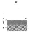
そこで、生化学物質間の結合を簡便に標識を用いることなく直接的に測定する方法として、光学薄膜の干渉色変化を利用した生化学センサは知られている。この生化学センサは、Sandstromらの論文(APPL.OPT.,24,472,1985)に述べられている。その例を図1を用いて説明する。基板1上に光学薄膜2を設ける。空気の屈折率は1.00であり、光学薄膜2が屈折率1.50の材料であり、基板の屈折率は2.25のものを用いている。光学薄膜の厚さを、可視光の波長λ0の4分の1またはその奇数倍(3/4λ0、5/4λ0など)の光学的長さとしておくと、光学薄膜は反射防止膜として働き、図2の反射スペクトルAのように、波長λ0で光学薄膜に垂直方向の反射光の強度が0となる。これにより、センサが干渉色を生じる。この光学薄膜2の上に、第1の生化学物質3の単分子層を設ける。生化学物質をタンパク質とすると、屈折率は1.5程度、層の厚さは10nm程度である。これにより、光にとっては光学薄膜が厚くなったことになり、反射スペクトルが図2の実線Aから点線A’のように変化し、干渉色が変化する。この第1の生化学物質3に第2の生化学物質4が生化学的に結合すると、更に膜厚が厚くなることになり、図2の点線A’から破線A’’の変化が生じ、干渉色が変化する。これにより、第2の生化学物質の結合が検出される。一般的な検出の手順は、まず基板1上の光学薄膜2を第1の生化学物質の単分子層3で覆ったものを準備する。これを第2の生化学物質の溶液の中に入れる。その後、溶液から取りだし、乾燥した後、図2の点線A’から破線A’’への干渉色の変化を調べる。このように従来はセンサを空気中に取り出して乾燥した後、干渉色を測定するものであった。
【0004】
【発明の解決しようとする課題】
しかしながら、上記論文に記載されたセンサで、検出するためには、一旦空気中に取り出して乾燥後に干渉色を測定するため、乾燥工程の時間がかかり、高スループット化が望めないという問題がある。
【0005】
また、反応開始後所定の時間経過後に測定を行うため、所定の時間の設定の仕方によっては、反応が飽和する前に空気中に取り出してしまうことも有るため、必ずしも精度のよい測定が行えない。一方で、反応が十分に飽和した後に測定するべく、所定の時間を長時間に設定した場合には、反応が飽和した後もセンサが溶液中に浸されているため、時間的効率が悪い。
【0006】
本発明の目的は、高スループットで生化学物質の結合を測定できる光学薄膜の光干渉効果を利用した簡便なセンサを提供することにある。
【0007】
【課題を解決するための手段】
上記目的は、以下の構成により、達成される。即ち、
(1)基板上に形成された光学薄膜と、その光学薄膜表面に形成されたプローブからなるセンサチップに、そのプローブと相互作用するサンプルを含む液を供給し、この液体が供給された状態で、相互作用の前後で変化する反射光の強度を検出する。ここで、光学薄膜としては、サンプルを含む水溶液の屈折率とは大きく異なるもの、即ち、屈折率が1.8以上のような酸化チタン、酸化ジルコニウム、酸化ハフニウム、酸化タンタルのようなものを用いる。このような、水溶液の屈折率とは大きく異なる屈折率の光学薄膜を用いれば、プローブとサンプルの反応前後で、光の干渉による強度変化を水中でも検出できる。なお、屈折率は3.0以下であると望ましい。理由は、上記材料の屈折率が3以下であることと、光学薄膜の屈折率が高いほど生化学物質の結合による干渉色の変化が小さくなるからである。また、この透明層の膜厚は、10nm以上10μm以下である。理由は、膜厚が10nm以下の場合には可視光領域に干渉色を得づらい。また、10μmよりも厚い場合は、反射スペクトルに現れる光干渉の構造が細かすぎるため本願のセンサには実用的ではない。
【0008】
ここで、本発明では主に、生化学物質間の結合を溶液中で光学薄膜の干渉色変化を利用して検出する。ここで、この生化学物質とは、他の物質に生化学的に結合する物質のことを指し、タンパク質、核酸、脂質、糖などの生体内で生産される物質だけではなく、薬剤物質、内分泌錯乱化学物質などの生体内の分子と結合する外来物質も含む。
【0009】
上記従来の生化学センサでは、大気中での測定であった。この大気中の測定では、Sandstromらの論文(APPL.OPT.,24,472,1985)にあるように、屈折率が1.5以上の光学薄膜がセンサに適するとされてきた。一方、サンプルを含む溶液としては、生化学物質等が含まれた水溶液である。この水溶液の屈折率は、生化学物質等の濃度によって変化するが、純水の屈折率である1.3330前後である。溶液中では、大気の屈折率1.0と比べて0.3以上背景の屈折率が高くなるために、従来のように屈折率が1.5程度の光学薄膜を用いたのでは、背景と光学薄膜の屈折率差による光の反射率が小さくなる。一方、本願では、光学薄膜の屈折率が1.8以上であり、純水の屈折率1.3330とは、0.467以上と、大きく異なるので、センサを乾燥させる前に、反応を十分に検出できるのである。更に、背景の屈折率が1.3330の時に明瞭な干渉色が現れる様に、基板または基板上の反射層を選ぶことで、より反応の検出が容易になる。
(2)また、基板上に、開口部を有する光学薄膜を設ける。ここで、開口部の内壁はプローブを固定化するために修飾されている。実際に検出する際には、プローブが固定化された開口部を有する光学薄膜が基板上に設けられたキットに、このプローブと相互作用する生化学物質を含むサンプルを流し、その相互作用を光を用いて検出する。
【0010】
ここでは、開口部の中の空間が、センサとして働く領域となるので、平坦な膜に比べてセンサとして働く領域が拡大するので、多くの生化学物質の結合により、干渉色のより大きい変化を得ることができる。
【0011】
開口の大きさ(直径)aは、タンパク質が入り込むために10nmより大きいことが望ましい。また、隣接する開口間の距離を光の波長以下にすることで、膜に平行な方向への構造が回折格子として働かないので、スペクトルが単純化される。従って、隣接する開口間の距離は、検出に用いる光の波長以下の距離が望ましい。また、凸部の大きさ(開口部間の間隔)bが小さいほうが、生化学物質の結合による実効的な光路長増加が大きくなる。これらのことから、可視光領域で検出するセンサの場合、望ましくは開口の大きさaは100〜400nmおよび凸部の大きさbは50〜350nmである。ここで、開口は円柱状とは限らない。例えば、逆に凸部を直径bの円柱状としても良いし、開口部を幅aのストライプ状の溝としても良い。
【0012】
このように、光学薄膜に開口部を設けた構成は、勿論、光学薄膜の屈折率が水溶液の屈折率と大きく異なる場合に用いることができるが、光学薄膜の上に半透明の反射層を加えることで、光学薄膜が、SiO2,ポリスチレン、PMMAのような屈折率が1.4〜1.6程度のもの、即ち背景である水の屈折率と比較的近いものを用いる場合でも、適用できる。
【0013】
なお、光学薄膜に開口部を設けた構成でも、反応前後で干渉色の変化が大きいために、水溶液を流した状態で干渉色変化を検出できる。
【0014】
この現象は、以下のようにして確認した。
【0015】
溶液中での検出のために、光学薄膜が溶液中で明瞭な干渉色を示すようにする。図1を用いて説明した屈折率2.25の基板1と屈折率1.5の光学薄膜2からなる構成では、センサの屈折率が溶液の屈折率n0と近くなるために、溶液と光学薄膜の間での光の反射が弱くなり、明瞭な干渉色が得られない。ここで、溶液としては主に生化学物質や塩、界面活性剤の水溶液が用いられる。純水の屈折率は、1.3330であり、水溶液の屈折率は生化学物質や塩、界面活性剤の濃度等により変化する。そこで、ここでは、溶液と光学薄膜との界面での光の反射を強くするために、光学薄膜上に薄い反射層を設ける。なお、光学薄膜の屈折率と水溶液の屈折率との差が十分有れば、反射層を設ける必要はない。その例を、図3に示す。基板5は屈折率1.5のガラスとし、その上に反射層6を設ける。ここでは反射層6を厚さ20nmのアルミニウムとした。そして、反射層6上に透明な材料からなる光学薄膜7を設ける。なお、基板5に光反射性のものを用いた場合には、反射膜6は省略できる。ここでは、屈折率1.5、厚さ150nmの透明な材料とした。その上に厚さ25nmの金からなる反射層8を設ける。ここでのn0は純水の屈折率1.3330とする。この構成では、図4および図5の実線Bで示した反射スペクトルの様に、波長605.5nmで反射層6と反射層8間の干渉効果で反射減衰により反射率が極小となる。ここで、図5は、図4の横軸の光の波長の565nmから655nmの範囲を拡大した図面である。以下、この極小を与える波長を反射減衰波長λARと呼ぶ。図3に示したように、反射層8の上に屈折率1.5、厚さ10nmの第1の生化学物質の層9が形成されたときの干渉色の変化を計算すると、図4および図5の実線Bから点線B’の変化を生じるもののλARが0.8nmしか変化しない。同様に、第1の生化学物質9への第2の生化学物質の結合を、第1の生化学物質9の上に屈折率1.5、厚さ10nmの第2の生化学物質の層が形成されたとして計算すると、λARはB’のλARから0.5nm長波長側へ変化するだけである。これは、干渉色が反射層6と反射層8との間の光干渉効果で特徴付けられているために、これら反射層の外に生化学物質層が加わったことによる屈折率の変化に対する干渉色の変化が小さいためだと考えられる。
【0016】
それに比べて、図3の透明層の屈折率が変化した場合には、敏感に
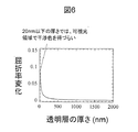
λARが変化する。図3の第1の生化学物質の層による屈折率の変化では、厚さ10nmにわたって背景の屈折率1.3330から1.5へ屈折率が変化する。このときの屈折率の変化量Δnは0.167である。Δnと厚さの積が同じになるように、すなわち同じ光路長の変化を与えるように透明層7の屈折率を変化させて、このときのλARの変化量の比較を行った。透明層7の厚さは150nmなので、この条件に基づいて透明層7の屈折率を0.011だけ増加させて反射スペクトルを計算した。図4および図5の破線B’’は、透明層7の屈折率を1.511としたときの反射スペクトルである。図4および図5の実線Bから破線B’’へのλARの変化量は、実線Bから点線B’ へのλARの変化量に比べて約6倍となり、4.7nmの長波長側への変化が得られた。同様に第2の生化学物質の結合に対するλARの変化量の比較も行った。透明層7の屈折率を1.511から更に0.011だけ増加させてλARを求めると、ここでも破線B’’から一点鎖線B'''に変化し、B’’のλARから4.7nmのλARの長波長側への変化を得た。可視光を用いて検出を行うための透明層7の厚さは、20nmから1.5μmの間である。なぜなら、20nm以下の厚さでは、主に紫外領域に干渉効果が現れるために、可視領域に干渉色を得づらい。また、1.5μm以上の厚さでは第2の生化学物質の結合量に対する干渉色の変化が小さくなるからである。これは、透明層7の厚さが150nmの場合には、0.011の屈折率変化であったが、図6に示すようにこの屈折率変化と透明層7の厚さの関係は反比例であり、1.5μm以上の厚さでは屈折率変化が小さく、従って干渉色の変化が小さくなるからである。このように反射層間の光路長変化を利用することで、より良い感度で生化学物質を検出することが期待できる。
【0017】
そこで、光学薄膜(透明層)の中に溶液と生化学物質を入れて屈折率を変化させることができるように、図7に示した様に、光学薄膜中に生化学物質が入るための開口10を設ける。このように開口を設けることで、膜に平行な方向に構造を持つ光学薄膜となる。このような構造を持つ光学薄膜からの光の反射は、例えば井上・大高らの誘電体球の2次元規則配列の光散乱の理論(Phys.Rev.B,25,689,1982)にあるように、構造に起因した複雑な光散乱現象が生じるが、第一近似的には、構造が持つ屈折率と水溶液の屈折率との平均化した膜の光干渉、即ち水の屈折率と開口部を有する透明層の屈折率の平均値の屈折率による光干渉が生じる。従って、開口10内に固定化された第1の生化学物質11への第2の生化学物質の結合により、実効的に反射層間の屈折率が増加することになり光路長の増加をもたらす。これにより、
λARは長波長側に変化する。
(3)更に、複数種類のプローブ毎に、光を照射し、その反射光を検出する光ファイバと、反射光の強度変化を計測する測定器を設けた検出装置によって達成される。
【0018】
ここでは、プローブの種類毎に光ファイバを設けるため、複数種の反応をほぼ同時に検出できる。
【0019】
【発明の実施の形態】
<実施例1>
以下、生化学物質間の結合を感度よく検出するためのセンサの製造方法を述べる。図14にセンサの製造方法の一例を示す。平坦な表面を持つ屈折率1.5のガラス基板14に、5nmの厚さのアルミニウムの反射層15を真空蒸着する。続いて、120nmの厚さの酸化チタン(TiOx、屈折率2.4)の透明層16を真空蒸着する。その後、3−アミノプロピルトリメトキシシランで表面処理を行い、透明層16の表面にアミノ基を導入する。そして、2mgのN−ヒドロキシスクシイミドと10mgの水溶性カルボジイミドと1mgの抗体を1mlの脱イオン水に溶かし抗体のカルボキシル基を活性化し、この溶液をアミノ基を導入した箇所に滴下して、抗体をセンサ表面のアミノ基に共有結合により固定化する。この後、脱イオン水でセンサチップをすすぎ、窒素ガスを吹きかけて乾燥する。
【0020】
このセンサは溶液中で明瞭な干渉色を示し、生化学物質の結合によりその干渉色が変化する。図15に計算機シミュレーションに用いたモデルを示す。背景の屈折率n0は1.3330とした。第一の生化学物質(プローブ)を、屈折率1.5、厚さ10nmの層17とした(図15(a))。この生化学センサに対し、第2の生化学物質を含むサンプルを供給することにより、第1の生化学物質と第2の生化学物質とを結合させる(図15(b))。この第2の生化学物質を、屈折率1.5、厚さ10nmの層18として示した。図16、図17および図18に反射スペクトルを示す。縦軸の反射減衰は、吸光度の計算の要領で、−log10Rとした。ここで、Rはセンサの反射率である。図16は、波長が400nmから830nmでの反射減衰を示し、図17は図16における波長575nmから585nmの部分的拡大図、図18は図16における波長510nmから610nmの部分的拡大図である。それぞれ、生化学物質層なしの反射スペクトルを実線Cで、第一の生化学物質層が施されたセンサの反射スペクトルを点線C'で、第2の生化学物質が結合した後の反射スペクトルを破線C''で示した。図16の反射スペクトルから、λARが550nm周辺であることが分かる。また、それぞれのスペクトルの概形は同じと分かる。反射減衰のピークの裾の部分で拡大した図17とλAR周辺を拡大した図18とで、結合前と結合後の変化を確認することができる。図17での変化からわかるように、単色光源を用いて、特定の波長でのセンサの反射強度の変化を測定することで第2の生化学物質の結合を検出することができる。一方、図18から分かるように、λARの位置が生化学物質の結合により長波長側に移動するのが分かる。この移動分を、定量的に示す方法を述べる。まず、反射スペクトルのλAR付近に沿う関数で近似する。その関数には、線形の関数と擬似Voigtピーク関数の和で表わされる。
【0021】
図19に結合前の反射スペクトルを近似した結果を破線で示した。近似はすべての定数及び係数に対して波長400nmから800nmの範囲で行った。良く近似できることがわかる。この近似から得られる擬似Voigtピーク関数の中心xcをλARとすることで、λARの位置を決定する。この方法によるλARの位置は、実線Cは551.21nm、実線C'は555.20nm、実線C’’は559.11nmであった。このように、第2の生化学物質の結合により、3.91nmのλARの変化を得ることができる。
<実施例2>
基板14に光反射性のもの、または透明層16と屈折率差が大きいものを用いる場合、反射層15なしでも基板14と透明層16の間で光の反射が生じるので、反射層15を省略することができる。この実施例2では、反射層を設けない例を示す。
【0022】
以下、このセンサの製造方法の一例を述べる。このセンサの製造は、平坦な表面を持つ屈折率1.5のガラス基板14に、120nmの厚さの酸化チタン(TiOx、屈折率2.4)の透明層16を真空蒸着することで得られる。上記と同じく、3−アミノプロピルトリメトキシシランで表面処理を行い、透明層16の表面にアミノ基を導入し、実施例1で述べた方法で第一の生化学物質を表面に固定化できる。
【0023】
図20、図21および図22に、図15と同様の条件、すなわち背景の屈折率を1.3330、第1および第2の生化学物質層を屈折率1.5、厚さ10nmの層とした計算機シミュレーションによる反射スペクトルとその変化を示す。それぞれ、生化学物質層なしの反射スペクトルを実線Dで、第一の生化学物質層が施されたセンサの反射スペクトルを点線D’で、第2の生化学物質が結合した後の反射スペクトルを破線D’’で示した。図20の反射スペクトルから、λARが580nm周辺であることが分かる。反射減衰のピークの裾の部分で拡大した図21とλAR周辺を拡大した図22とで、結合前と結合後の反射スペクトルの変化を確認することができる。図21での変化からわかるように、単色光源を用いて、特定の波長でのセンサの反射強度の変化を測定することで第2の生化学物質の結合を検出することができる。一方、図22から分かるように、
λARの位置が生化学物質の結合により長波長側に移動するのが分かる。実施例1と同様の近似を波長470nmから800nmの範囲で行うことで求められる第2の生化学物質の結合によるλARの変化量は5.38nmで、上記センサとほぼ同程度の検出感度である。また、透明な基板14を用いているので、この反射スペクトルの変化は基板側からの光照射による反射スペクトルの測定によっても実施できる。透明層16の屈折率が2.4以外の場合との感度の比較のために、図23にλARの変化量の透明層16の屈折率依存性を示す。ここで、透明層16の厚さは透明層16の厚さとその屈折率の積が一定となるように決めた。図23から分かるように、透明層16の屈折率が高いほどλARの変化が小さくなる。なお、透明層16の屈折率が1.8より小さい領域では、水溶液との屈折率差が小さくなるため、非常に検出しづらい。図24に透明層16の屈折率を1.6から2.4の範囲で変化させて水(屈折率1.3330)中でのセンサの反射スペクトルを計算した結果を示す。ここでも、図23の場合と同様に透明層16の厚さは透明層16の厚さとその屈折率の積が一定となるように決めた。各屈折率と反射スペクトルの対応は図中に示した。屈折率の減少に伴いセンサの反射率が減少するのがわかる。屈折率が1.8より小さい領域では、センサの反射率が数%以下しかないので、非常に検出しづらくなる。
<実施例3>
本実施例では、透明層に開口部を設けた実施例を示す。
【0024】
図8はセンサチップの製造方法の一例を示すものである。以下、図8を用いて、センサの製造方法を述べる。基板5には、大きさ26mm×20mm、厚さ0.4〜0.6mmの血球計算用カバーガラスを用いた。ガラス基板表面(図8(a))に20nmの厚さのゲルマニウムを真空蒸着し反射層6を得た(図8(b))。透明層7を形成するために、超LSI用低誘電率層間膜材料HSG−R7(日立化成(株))をゲルマニウム層の上にスピンコートした(図8(c))。得られた透明層の厚さは約200nmであった。サブミクロンスケールでの開口10形成のために、サブミクロンサイズのシリカビーズを用いたナチュラルリソグラフィーを採用した。シリカビーズ12の単層膜を透明層7の上に設け(図8(d))、酸素ガスによる反応性イオンエッチングでHSG−R7の透明層7とシリカビーズ12のエッチング速度の違いを利用し、透明層7を選択的に膜に垂直方向に異方性ドライエッチングして開口10を得た(図8(e))。ドライエッチング後、エタノールを染み込ませたレンズクリーニングペーパーで表面のシリカビーズ12をふき取った(図8(f))。この表面に接着のための厚さ3nmのクロムと反射層8となる厚さ20nmの金を真空蒸着した(図8(g))。以上により、開口10内部にも金が蒸着されるが、透明層7を挟む金とゲルマニウムの反射層間の光干渉効果により発色し、センサとして図7に示した構造と本質的に同じ効果が得られる。図9に作製されたセンサチップの上面図を示す。上記方法によって、基板5の上に、直径約3mmの4つのセンサ部13を4mm間隔で一列に設けた。センサ部13は赤く発色した。これは、センサ部13のλARが530nm周辺であることから、赤い光が強く反射されるためである。以下、このセンサへの第1の生化学物質11の固定化の一例として、抗体の固定化法の手順を述べる。上記センサチップを0.1mMの11−アミノ−1−ウンデカンチオールのエタノール溶液に10時間以上浸した。これにより、真空蒸着された金表面に11−アミノ−1−ウンデカンチオールの自己組織化膜が形成され、開口10内部も含めた表面にアミノ基が導入された。2mgのN−ヒドロキシスクシイミドと10mgの水溶性カルボジイミドと1mgの抗体を1mlの脱イオン水に溶かし抗体のカルボキシル基を活性化し、この溶液をアミノ基を導入したセンサ部13に滴下して、抗体をセンサ表面のアミノ基に共有結合により固定化した。この後、脱イオン水でセンサチップをすすぎ、窒素ガスを吹きかけて乾燥した。
【0025】
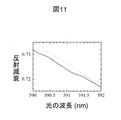
以下、上記の方法で製作されたセンサチップを用いた、タンパク質とそのタンパク質に結合する抗体の相互作用測定を述べる。タンパク質にはAVIDIN D(Vector Laboratories社)を、抗体にはANTI−AVIDIN D(Vector Laboratories社)を用いた。抗体を、上記に述べた方法でセンサ表面に固定化した。試料溶液は1mg/ml(約10μM)のタンパク質(AVIDIN D)のPBS溶液とした。この試料溶液をセンサ表面に約4分間流した。この時間の間にタンパク質と抗体の結合は飽和する。図10、図11および図12に、タンパク質結合前のPBS緩衝液中での反射スペクトルを実線で、タンパク質結合後の反射スペクトルを点線で示す。縦軸の反射減衰は、吸光度の計算の要領で、−log10(I/I0)+αとした。ここで、Iはセンサの反射光の強度、I0は標準白色板の反射強度、αは定数である。図10は、波長400nmから900nmの反射減衰を示す図であり、図11は、590nmから592nmの反射減衰を示す図10の拡大図、図12は、波長510nmから波長550nmの反射減衰を示す図10の拡大図である。図10から分かるように、λARが約530nmに現れた。また、図10では結合前と結合後の反射スペクトルが重なっており、スペクトルの概形がほとんど同じと分かる。しかし、反射減衰のピークの裾の部分で拡大した図11とλAR周辺を拡大した図12とで、結合前と結合後の変化を確認することができる。図11での反射強度の変化からわかるように、単色光源を用いて、特定の波長でのセンサの反射強度の変化を測定することで第2の生化学物質の結合を検出することが可能である。ここで、図11の実線、点線が滑らかではないのは、単色光源を用いた検出のための評価を行うために、図11の反射スペクトルには波長方向の平滑化を行わなかったからである。
一方、図12からλARが変化しているのが分かるが、これを定量的に示すため、処理した。図13に結合前の反射スペクトルを近似した結果を破線で示した。近似は、波長470nmから900nmの範囲で行った。良く近似できることが分かる。この近似から得られる関数の中心をλARとした。この方法により求められたλARは結合前が530.28nm、結合後は530.35nmである。このようにλARの変化から、タンパク質と抗体の結合を検出することもできる。
<実施例4>
以下、本発明の光学薄膜センサの干渉色変化を溶液中でリアルタイムに検出する装置を、図面を用いて説明する。図25は、本発明の一実施例を示すブロック図、図26は本発明の検出装置の計算機の表示画面の一実施例を示す図、図27は、本発明の検出装置の光学系の一実施例を示す斜視図、図28は本発明の検出装置の反応槽の一実施例を示す斜視図、図29は図28のE−E'での断面図、図30は図28のF−F'での断面図である。
【0026】
本発明の検出装置は、図25のように、タングステンランプなどの白色光源19からの光が光ファイバからなる照射光学系20を経て、反応槽21に入った基板22上の実施例1〜実施例3で述べた光学薄膜センサ部23複数に照射され、その光学薄膜センサ部23からの反射光が光ファイバからなる集光光学系24を経て、複数の分光器25と複数のCCDやフォトダイオードアレイなどの多チャンネル受光機26でリアルタイムに反射スペクトルとして測定され、計算機27に反射スペクトルのデータが取りこまれる。計算機27により、実施例1〜3で述べた、光学薄膜センサ部23の反射スペクトルの反射減衰の曲線に沿う関数(1)での最小自乗法による近似を自動的に行い、図26のグラフ28のように表示する。この近似から得られる関数の極値を与える波長、すなわちλARを時間に対して図26のグラフ29の様にリアルタイムにプロットし記録する。通常、CCDやフォトダイオードアレイなどの多チャンネル受光機のピクセルの間隔により、測定できる波長の間隔は制限されるが、近似の計算結果の波長位置をプロットすることで、より細かくλARを決定できる。すなわち、結合量の計測のダイナミックレンジを拡大することができる。また、通常、同じ多チャンネル受光機26を用いてより細かくλARを決定するには、より長い分光器を要する。よって、この近似の計算により、通常よりも短い分光器で同程度のダイナミックレンジが得られることから、装置の小型化ができる。さらに、通常、CCDやフォトダイオードアレイなどの多チャンネル受光機26で生じる雑音が反射スペクトルに反映されるが、この関数による近似は雑音を平均化するので、S/N比の向上につながり、実効的なダイナミックレンジを拡大することができる。グラフ29の時間微分をグラフ30に表示し記録する。これにより、結合の開始と、飽和が分かり易くなる。
【0027】
図27に光ファイバを用いた照射光学系20、集光光学系24の一実施例を示す。直径2mmの金属のパイプ31に直径30ミクロンのガラス製の光ファイバが詰まった光ファイバ束を用意する。光ファイバ束の中心部分を占める光ファイバ32の反対側の端は、分光器25のスリットの前に置かれる。光ファイバ束の外側部分を占める光ファイバ33の反対側の端は、白色光源19の前に置かれる。
【0028】
図28,29,30に、図27に示したバンドルファイバ34を用いた検出装置の一実施例を示す。図28,29,30のように、バンドルファイバ34を反応槽21と冷却水または温水35を循環させることで温調を行う冷却・加熱機36を固定した台37に取りつけられた可動台38に固定し、光学薄膜センサ部23の直上に置く。このようにして、それぞれのバンドルファイバ34からそれぞれの真下の光学薄膜センサ部23に光が照射されるようにする。可動台38にはバンドルファイバ34の光学薄膜センサ部23に対する位置が再現されるように、停止機構39が取り付けられる。一般に、光学薄膜の干渉色は測定に用いる光の入射・反射角度に依存する。停止機構39を利用してバンドルファイバ34の位置を再現することで、照射光学系20用の光ファイバ33から照射される光と光学薄膜センサ部23で反射され集光光学系24用の光ファイバ32で集光される光の角度が再現される。使用する光ファイバの開口数から決まる光照射角、集光角の範囲内でこの角度を決めて使用するのが望ましい。また、図27のように集光用光ファイバ32を照射用光ファイバ33が囲む配置にすることで、光学薄膜センサ部23に対するバンドルファイバ34の取りつけの傾きがある場合に、その影響がその配置により平均化されるので、得られる反射スペクトルの再現性が良くなる。一度により多くの種類の生化学物質の結合を調べるには、光学薄膜センサ部23とバンドルファイバ34の数を増やすことで対応できる。バンドルファイバ34の先端と反応槽の窓40の間に液体を入れるための空間41を設ける。これにより、バンドルファイバ34の先端および反応槽の窓40での界面の光の反射を低減でき、反射スペクトル測定への影響を少なくできる。また、冷却時に反応槽21の周りに水滴や霜が付着することがあるが、この空間41に液体を入れることで水滴や霜の付着による反射スペクトル測定への影響を防ぐことができる。反応槽21をつや消し黒で塗装した。これにより、反応槽内での散乱光や室内光の集光光学系24への入射を防ぐことができる。溶液の入り口42から溶液の出口43へ送液ポンプとサンプルインジェクターなどを用いて生化学物質を含む試料溶液44を反応槽21へ送液し、ある時間の間だけ生化学物質を含む試料溶液44が反応槽を通過する状態を作ることで、生化学物質の結合および解離のリアルタイム検出を行うことができる。反応槽の上方に、溶液の入り口42および溶液の出口43を配置し、溶液の入り口42側に気泡を取り除くための空間45を設けることで、対象生化学物質を含む試料溶液44に気泡が含まれていた場合に、その気泡の反応槽21への進入を防ぐことができ、また、気泡が反応槽21に進入した場合や発生した場合には、その排出を促進することができる。一般に生化学物質間の結合には、環境の温度依存性がある。冷却・加熱機36により反応槽21の温度を調節し、対象生化学物質の結合の温度依存性を調べることができる。冷却・加熱機36はペルティエ素子などでもよい。
【0029】
図31に、実施例3で述べたセンサと本検出装置を用いたλARの変化のリアルタイム測定の結果を示す。センサ表面に固定化した抗体、固定化法、試料溶液については実施例3で述べたとおりである。図31のGまでの時間はセンサ表面にPBS緩衝液が送液されている。このPBS緩衝液送液中のλARは530.30nmであった。縦軸はλARの530.30nmからの変化量を表わしている。図31のGで示した時点からAVIDIN DのPBS溶液がセンサ上を流れ結合が始まり、破線で示した指数関数に沿うようにλARが増加している。これにより、結合量の飽和が確かめられた。Hで示した時点で、10mMの塩酸を送液し結合を解離させたところ、解離の後は元のλARに戻った。結合と解離の測定に要した時間は、約20分であった。タンパク質結合によるλARの変化量が0.07nmと小さいのは、結合したAVIDIN Dの量が単層膜を形成するほど密ではなかったからだと考えられる。
【0030】
なお、このリアルタイムで反射光を検出する方法については、上記実施例1、2のように、開口部を形成しない屈折率の大きな光学薄膜を用いる場合でも、開口部を形成する実施例3の場合にも、用いることができる。
【0031】
この実施例では、リアルタイムで反応が検出できるので、より高スループットで生化学物質の結合を測定できる。
【0032】
【発明の効果】
上記構成により、高スループットで、精度良く、生化学物質の結合を測定できる。
【図面の簡単な説明】
【図1】 従来の生化学センサの構成を示す図。
【図2】 従来の生化学センサの干渉色変化を示す図。
【図3】 本発明の原理を示す図。
【図4】 本発明の干渉色変化を示す図。
【図5】 本発明の干渉色変化を示す図。
【図6】 本発明の原理を示す図。
【図7】 本発明の生化学センサの構成を示す図。
【図8】 本発明の生化学センサの製造工程図。
【図9】 本発明の生化学センサの上面図。
【図10】 蛋白結合前と結合後の反射減衰を示す図。
【図11】 蛋白結合前と結合後の反射減衰を示す図。
【図12】 蛋白結合前と結合後の反射減衰を示す図。
【図13】 蛋白結合前の反射スペクトルを近似した図。
【図14】 本発明の生化学センサの製造工程図。
【図15】 本発明の生化学センサの構成を示す図。
【図16】 本発明の干渉色変化を示す図。
【図17】 本発明の干渉色変化を示す図。
【図18】 本発明の干渉色変化を示す図。
【図19】 結合前の反射スペクトルを近似した図。
【図20】 本発明の干渉色変化を示す図。
【図21】 本発明の干渉色変化を示す図。
【図22】 本発明の干渉色変化を示す図。
【図23】 本発明の生化学センサの感度を示す図。
【図24】 本発明の生化学センサの反射スペクトルを示す図。
【図25】 本発明の装置を示すブロック図。
【図26】 本発明の検出装置の計算機の表示画面を示す図。
【図27】 本発明の検出装置の光学系を示す斜視図。
【図28】 本発明の検出装置の反応槽を示す斜視図。
【図29】 図28のE−E'での断面図。
【図30】 図28のF−F'での断面図。
【図31】 本発明の検出装置を用いた測定結果を示す図。
【符号の説明】
1:基板、2:光学薄膜、3:第1の生化学物質、4:第2の生化学物質、5:基板、6:反射層、7:光学薄膜、8:反射層、9:第1の生化学物質、10:開口部、11:第1の生化学物質、12:シリカビーズ、13:センサ部。[0001]
BACKGROUND OF THE INVENTION
The present invention relates to a biochemical sensor using an optical thin film, a sensor member, and a measuring apparatus using the same.
[0002]
[Prior art]
Conventionally, measurement of binding between biochemical substances such as antigen-antibody reaction has been generally performed by using a label such as a radioactive substance or a fluorescent substance. This labeling takes time, and in particular, labeling a protein may involve complicated methods or the property of the protein may change depending on the labeling.
[0003]
Therefore, biochemical sensors using interference color change of an optical thin film are known as a method for directly measuring the binding between biochemical substances without using a label. This biochemical sensor is described in Sandstrom et al. (APPL. OPT.,24472, 1985). An example of this will be described with reference to FIG. An optical
[0004]
[Problem to be Solved by the Invention]
However, in order to detect with the sensor described in the above paper, since the interference color is once measured after being taken out into the air and dried, there is a problem that it takes time for the drying process and high throughput cannot be expected.
[0005]
In addition, since measurement is performed after a predetermined time has elapsed after the start of the reaction, depending on how the predetermined time is set, it may be taken out into the air before the reaction is saturated, so accurate measurement cannot always be performed. . On the other hand, if the predetermined time is set to a long time so as to perform measurement after the reaction is sufficiently saturated, the sensor is immersed in the solution even after the reaction is saturated, so that the time efficiency is poor.
[0006]
An object of the present invention is to provide a simple sensor using the optical interference effect of an optical thin film that can measure the binding of biochemical substances with high throughput.
[0007]
[Means for Solving the Problems]
The above object is achieved by the following configuration. That is,
(1) A liquid containing a sample that interacts with the probe is supplied to a sensor chip including an optical thin film formed on the substrate and a probe formed on the surface of the optical thin film, and the liquid is supplied. The intensity of the reflected light that changes before and after the interaction is detected. Here, as the optical thin film, one that is significantly different from the refractive index of the aqueous solution containing the sample, that is, one such as titanium oxide, zirconium oxide, hafnium oxide, tantalum oxide having a refractive index of 1.8 or more is used. . If such an optical thin film having a refractive index significantly different from the refractive index of the aqueous solution is used, a change in intensity due to light interference can be detected in water before and after the reaction between the probe and the sample. The refractive index is desirably 3.0 or less. The reason is that the refractive index of the material is 3 or less, and the higher the refractive index of the optical thin film, the smaller the change in interference color due to the binding of biochemical substances. The film thickness of this transparent layer is 10 nm or more and 10 μm or less. The reason is that it is difficult to obtain an interference color in the visible light region when the film thickness is 10 nm or less. On the other hand, if it is thicker than 10 μm, the structure of optical interference appearing in the reflection spectrum is too fine, which is not practical for the sensor of the present application.
[0008]
Here, in the present invention, the binding between the biochemical substances is mainly detected in the solution using the interference color change of the optical thin film. Here, this biochemical substance refers to a substance that binds biochemically to other substances, and not only substances produced in vivo such as proteins, nucleic acids, lipids, and sugars, but also drug substances and endocrine secretions. Also includes foreign substances that bind to molecules in the body, such as confusion chemicals.
[0009]
In the conventional biochemical sensor, measurement was performed in the atmosphere. In this atmospheric measurement, Sandstrom et al. (APPL. OPT.,24472, 1985), an optical thin film having a refractive index of 1.5 or more has been considered suitable for a sensor. On the other hand, the solution containing the sample is an aqueous solution containing a biochemical substance or the like. The refractive index of this aqueous solution varies depending on the concentration of the biochemical substance or the like, but is around 1.3330, which is the refractive index of pure water. In the solution, since the refractive index of the background is higher by 0.3 or more than the refractive index of 1.0 in the atmosphere, using an optical thin film having a refractive index of about 1.5 as in the past, the background and The light reflectance due to the refractive index difference of the optical thin film is reduced. On the other hand, in this application, the refractive index of the optical thin film is 1.8 or more, and the refractive index of pure water 1.3330 is significantly different from 0.467 or more. It can be detected. Furthermore, the reaction can be detected more easily by selecting the substrate or the reflective layer on the substrate so that a clear interference color appears when the background refractive index is 1.3330.
(2) An optical thin film having an opening is provided on the substrate. Here, the inner wall of the opening is modified to immobilize the probe. In actual detection, a sample containing a biochemical substance that interacts with the probe is passed through a kit in which an optical thin film having an opening to which the probe is immobilized is provided on the substrate, and the interaction is optically detected. To detect.
[0010]
Here, since the space inside the opening becomes a region that acts as a sensor, the region that acts as a sensor is expanded compared to a flat film, so that a larger change in interference color is caused by the binding of many biochemical substances. Obtainable.
[0011]
The size (diameter) a of the opening is desirably larger than 10 nm in order to allow protein to enter. Further, by setting the distance between adjacent openings to be equal to or less than the wavelength of light, the structure in the direction parallel to the film does not work as a diffraction grating, so that the spectrum is simplified. Therefore, the distance between adjacent openings is preferably a distance equal to or smaller than the wavelength of light used for detection. In addition, the smaller the size of the convex portion (interval between openings) b, the larger the effective optical path length increase due to the binding of biochemical substances. For these reasons, in the case of a sensor that detects in the visible light region, the size of the opening a is preferably 100 to 400 nm and the size b of the convex portion is 50 to 350 nm. Here, the opening is not necessarily cylindrical. For example, conversely, the convex portion may be a columnar shape having a diameter b, and the opening portion may be a stripe-shaped groove having a width a.
[0012]
As described above, the structure in which the opening is provided in the optical thin film can be used when the refractive index of the optical thin film is significantly different from the refractive index of the aqueous solution, but a semitransparent reflective layer is added on the optical thin film. Therefore, the optical thin film is made of SiO.2, Polystyrene, PMMA and the like having a refractive index of about 1.4 to 1.6, that is, a material having a refractive index relatively close to that of water as a background can be used.
[0013]
Even in the configuration in which the opening is provided in the optical thin film, the change in interference color is large before and after the reaction, so that the change in interference color can be detected in a state where an aqueous solution is flowed.
[0014]
This phenomenon was confirmed as follows.
[0015]
For detection in solution, the optical thin film should have a clear interference color in solution. In the configuration comprising the
[0016]
In contrast, when the refractive index of the transparent layer in FIG.
λARChanges. The refractive index change due to the first biochemical layer of FIG. 3 changes the refractive index from the background refractive index of 1.3330 to 1.5 over a thickness of 10 nm. At this time, the refractive index change Δn is 0.167. The refractive index of the
[0017]
Therefore, as shown in FIG. 7, an opening for the biochemical substance to enter the optical thin film so that the refractive index can be changed by putting the solution and the biochemical substance in the optical thin film (transparent layer). 10 is provided. By providing the opening in this manner, an optical thin film having a structure in a direction parallel to the film is obtained. The reflection of light from the optical thin film having such a structure is, for example, the theory of light scattering of a two-dimensional regular array of dielectric spheres by Inoue and Otaka (Phys. Rev. B,25, 689, 1982), a complicated light scattering phenomenon due to the structure occurs, but in the first approximation, the optical interference of the film obtained by averaging the refractive index of the structure and the refractive index of the aqueous solution, That is, optical interference occurs due to the refractive index of the average value of the refractive index of water and the refractive index of the transparent layer having the opening. Therefore, the coupling of the second biochemical substance to the first
λARChanges to the longer wavelength side.
(3) Furthermore, this is achieved by a detection device provided with an optical fiber that irradiates light for each of a plurality of types of probes and detects the reflected light, and a measuring instrument that measures a change in the intensity of the reflected light.
[0018]
Here, since an optical fiber is provided for each type of probe, a plurality of types of reactions can be detected almost simultaneously.
[0019]
DETAILED DESCRIPTION OF THE INVENTION
<Example 1>
Hereinafter, a method for manufacturing a sensor for sensitively detecting a bond between biochemical substances will be described. FIG. 14 shows an example of a sensor manufacturing method. A
[0020]
This sensor shows a clear interference color in solution, and the interference color changes due to the binding of biochemical substances. FIG. 15 shows a model used for computer simulation. Refractive index n of background0Was 1.3330. The first biochemical substance (probe) was a
[0021]
In FIG. 19, the result of approximating the reflection spectrum before coupling is shown by a broken line. The approximation was performed in the wavelength range of 400 nm to 800 nm for all constants and coefficients. It can be seen that it can be approximated well. The center x of the pseudo-Voigt peak function obtained from this approximationcΛARSo that λARDetermine the position. Λ by this methodARThe solid line C was 551.21 nm, the solid line C ′ was 555.20 nm, and the solid line C ″ was 559.11 nm. In this way, λ of 3.91 nm is obtained by the binding of the second biochemical substance.ARChange.
<Example 2>
When the
[0022]
Hereinafter, an example of a manufacturing method of this sensor will be described. This sensor can be manufactured by vacuum-depositing a
[0023]
20, 21, and 22, the same conditions as in FIG. 15, that is, the background refractive index is 1.3330, the first and second biochemical layers are layers having a refractive index of 1.5 and a thickness of 10 nm. Shows the reflection spectrum and its change by computer simulation. The reflection spectrum without the biochemical substance layer is indicated by a solid line D, the reflection spectrum of the sensor provided with the first biochemical substance layer is indicated by a dotted line D ′, and the reflection spectrum after the second biochemical substance is combined is shown. This is indicated by a broken line D ″. From the reflection spectrum of FIG.ARIs around 580 nm. FIG. 21 and λ enlarged at the bottom of the peak of return lossARWith FIG. 22 in which the periphery is enlarged, it is possible to confirm the change in the reflection spectrum before and after the combination. As can be seen from the change in FIG. 21, the binding of the second biochemical substance can be detected by measuring the change in the reflection intensity of the sensor at a specific wavelength using a monochromatic light source. On the other hand, as can be seen from FIG.
λARIt can be seen that the position of moves to the longer wavelength side due to the binding of biochemical substances. Λ by the binding of the second biochemical substance obtained by performing the same approximation as in Example 1 in the wavelength range of 470 nm to 800 nm.ARThe amount of change is 5.38 nm, which is approximately the same sensitivity as the above sensor. Further, since the
<Example 3>
In this example, an example in which an opening is provided in a transparent layer is shown.
[0024]
FIG. 8 shows an example of a sensor chip manufacturing method. The sensor manufacturing method will be described below with reference to FIG. For the
[0025]
Hereinafter, measurement of interaction between a protein and an antibody that binds to the protein using the sensor chip manufactured by the above method will be described. AVIDIN D (Vector Laboratories) was used as the protein, and ANTI-AVIDIN D (Vector Laboratories) was used as the antibody. The antibody was immobilized on the sensor surface by the method described above. The sample solution was a 1 mg / ml (about 10 μM) protein (AVIDIND) solution in PBS. This sample solution was allowed to flow over the sensor surface for about 4 minutes. During this time, protein and antibody binding saturates. In FIG. 10, FIG. 11 and FIG. 12, the reflection spectrum in the PBS buffer before protein binding is shown by a solid line, and the reflection spectrum after protein binding is shown by a dotted line. The reflection loss on the vertical axis is the procedure for calculating the absorbance.10(I / I0) + Α. Here, I is the intensity of reflected light from the sensor, I0Is the reflection intensity of the standard white plate, and α is a constant. FIG. 10 is a diagram showing reflection attenuation from a wavelength of 400 nm to 900 nm, FIG. 11 is an enlarged view of FIG. 10 showing reflection attenuation from 590 nm to 592 nm, and FIG. 12 is a diagram showing reflection attenuation from a wavelength of 510 nm to 550 nm. 10 is an enlarged view of FIG. As can be seen from FIG.ARAppeared at about 530 nm. Further, in FIG. 10, the reflection spectra before and after the combination are overlapped, and it can be seen that the outlines of the spectra are almost the same. However, FIG. 11 and λ enlarged at the bottom of the reflection attenuation peak are shown.ARWith FIG. 12 in which the periphery is enlarged, it is possible to confirm changes before and after the combination. As can be seen from the change in reflection intensity in FIG. 11, it is possible to detect the binding of the second biochemical substance by measuring the change in the reflection intensity of the sensor at a specific wavelength using a monochromatic light source. is there. Here, the solid line and the dotted line in FIG. 11 are not smooth because the reflection spectrum in FIG. 11 was not smoothed in the wavelength direction in order to perform evaluation for detection using a monochromatic light source.
on the other handFrom FIG.ARCan be seen, but to show this quantitatively,Processed. In FIG. 13, the result of approximating the reflection spectrum before coupling is shown by a broken line. The approximation was performed in the wavelength range of 470 nm to 900 nm. It can be seen that it can be approximated well. The center of the function obtained from this approximation is λARIt was. Λ obtained by this methodARIs 530.28 nm before bonding and 530.35 nm after bonding. Thus λARFrom these changes, the binding between the protein and the antibody can also be detected.
<Example 4>
Hereinafter, an apparatus for detecting an interference color change of an optical thin film sensor of the present invention in a solution in real time will be described with reference to the drawings. FIG. 25 is a block diagram showing an embodiment of the present invention, FIG. 26 is a diagram showing an embodiment of a display screen of a computer of the detection apparatus of the present invention, and FIG. 27 is an optical system of the detection apparatus of the present invention. FIG. 28 is a perspective view showing an example, and FIG. 28 is a reaction of the detection apparatus of the present invention.TankFIG. 29 is a sectional view taken along the line EE ′ of FIG. 28, and FIG. 30 is a sectional view taken along the line FF ′ of FIG.
[0026]
As shown in FIG. 25, the detection apparatus of the present invention reacts with light from a
[0027]
FIG. 27 shows an embodiment of the irradiation
[0028]
28, 29, and 30 show an embodiment of a detection device using the
[0029]
FIG. 31 shows the λ using the sensor described in Example 3 and the present detection device.ARThe result of real-time measurement of the change of is shown. The antibody immobilized on the sensor surface, the immobilization method, and the sample solution are as described in Example 3. During the time period up to G in FIG. 31, the PBS buffer solution is fed to the sensor surface. Λ in this PBS buffer solutionARWas 530.30 nm. The vertical axis is λARRepresents the amount of change from 530.30 nm. From the point of time indicated by G in FIG. 31, the AVIDIN D PBS solution flows on the sensor and starts to be coupled.ARHas increased. Thereby, the saturation of the amount of binding was confirmed. At the time indicated by H, 10 mM hydrochloric acid was fed to dissociate the bond, and after dissociation, the original λARReturned to. The time required for measurement of binding and dissociation was about 20 minutes. Λ by protein bindingARIt is considered that the amount of change in A is as small as 0.07 nm because the amount of the combined AVIDIND is not so dense as to form a single layer film.
[0030]
The method for detecting reflected light in real time is the case of Example 3 in which an opening is formed even when an optical thin film having a large refractive index that does not form an opening is used as in Examples 1 and 2 above. Can also be used.
[0031]
In this embodiment, since the reaction can be detected in real time, the binding of the biochemical substance can be measured with higher throughput.
[0032]
【The invention's effect】
With the above configuration, the binding of biochemical substances can be measured with high throughput and high accuracy.
[Brief description of the drawings]
FIG. 1 is a diagram showing a configuration of a conventional biochemical sensor.
FIG. 2 is a diagram showing a change in interference color of a conventional biochemical sensor.
FIG. 3 is a diagram showing the principle of the present invention.
FIG. 4 is a diagram showing a change in interference color according to the present invention.
FIG. 5 is a diagram showing a change in interference color according to the present invention.
FIG. 6 is a diagram showing the principle of the present invention.
FIG. 7 is a diagram showing a configuration of a biochemical sensor of the present invention.
FIG. 8 is a production process diagram of the biochemical sensor of the present invention.
FIG. 9 is a top view of the biochemical sensor of the present invention.
FIG. 10 is a diagram showing reflection attenuation before and after protein binding.
FIG. 11 is a diagram showing reflection attenuation before and after protein binding.
FIG. 12 is a diagram showing reflection attenuation before and after protein binding.
FIG. 13 is a diagram approximating a reflection spectrum before protein binding.
FIG. 14 is a production process diagram of the biochemical sensor of the present invention.
FIG. 15 is a diagram showing a configuration of a biochemical sensor of the present invention.
FIG. 16 is a diagram showing a change in interference color according to the present invention.
FIG. 17 is a diagram showing a change in interference color according to the present invention.
FIG. 18 is a diagram showing a change in interference color according to the present invention.
FIG. 19 is a diagram approximating a reflection spectrum before combining.
FIG. 20 is a diagram showing a change in interference color according to the present invention.
FIG. 21 is a diagram showing a change in interference color according to the present invention.
FIG. 22 is a diagram showing a change in interference color according to the present invention.
FIG. 23 is a graph showing the sensitivity of the biochemical sensor of the present invention.
FIG. 24 shows a reflection spectrum of the biochemical sensor of the present invention.
FIG. 25 is a block diagram showing an apparatus of the present invention.
FIG. 26 is a diagram showing a display screen of a computer of the detection apparatus of the present invention.
FIG. 27 is a perspective view showing an optical system of the detection apparatus of the present invention.
FIG. 28 shows the reaction of the detection apparatus of the present invention.TankFIG.
29 is a cross-sectional view taken along line EE ′ of FIG. 28. FIG.
30 is a cross-sectional view taken along the line FF ′ of FIG. 28. FIG.
FIG. 31 is a view showing a measurement result using the detection apparatus of the present invention.
[Explanation of symbols]
1: substrate, 2: optical thin film, 3: first biochemical substance, 4: second biochemical substance, 5: substrate, 6: reflective layer, 7: optical thin film, 8: reflective layer, 9: first 10: opening, 11: first biochemical substance, 12: silica beads, 13: sensor part.
Claims (10)
基板と、前記基板上に形成された、屈折率が1.8以上の光学薄膜と、前記光学薄膜に形成された第1の生化学物質からなるセンサチップを準備し、
前記センサチップに、前記第1の生化学物質と結合する第2の生化学物質を含む水溶液を供給し、
前記センサチップに光を照射し、
前記センサチップが乾燥する前の状態で、前記センサチップからの反射光を検出し、
前記反射光について、反射減衰により反射率が極小となる波長の変化量を測定する工程を有することを特徴とする測定方法。A detection method for detecting biochemical substances,
Preparing a sensor chip comprising a substrate, an optical thin film having a refractive index of 1.8 or more formed on the substrate, and a first biochemical substance formed on the optical thin film;
Supplying an aqueous solution containing a second biochemical substance that binds to the first biochemical substance to the sensor chip;
Irradiating the sensor chip with light,
In a state before the sensor chip is dried, the reflected light from the sensor chip is detected,
A method for measuring the reflected light, comprising measuring a change amount of a wavelength at which the reflectance becomes minimum due to reflection attenuation .
Priority Applications (2)
| Application Number | Priority Date | Filing Date | Title |
|---|---|---|---|
| JP2002296870A JP3786073B2 (en) | 2002-10-10 | 2002-10-10 | Biochemical sensor kit and measuring device |
| US10/372,288 US7439073B2 (en) | 2002-10-10 | 2003-02-25 | Kit for biochemical sensor and measuring apparatus |
Applications Claiming Priority (1)
| Application Number | Priority Date | Filing Date | Title |
|---|---|---|---|
| JP2002296870A JP3786073B2 (en) | 2002-10-10 | 2002-10-10 | Biochemical sensor kit and measuring device |
Publications (3)
| Publication Number | Publication Date |
|---|---|
| JP2004132799A JP2004132799A (en) | 2004-04-30 |
| JP2004132799A5 JP2004132799A5 (en) | 2005-06-23 |
| JP3786073B2 true JP3786073B2 (en) | 2006-06-14 |
Family
ID=32064173
Family Applications (1)
| Application Number | Title | Priority Date | Filing Date |
|---|---|---|---|
| JP2002296870A Expired - Lifetime JP3786073B2 (en) | 2002-10-10 | 2002-10-10 | Biochemical sensor kit and measuring device |
Country Status (2)
| Country | Link |
|---|---|
| US (1) | US7439073B2 (en) |
| JP (1) | JP3786073B2 (en) |
Cited By (10)
| Publication number | Priority date | Publication date | Assignee | Title |
|---|---|---|---|---|
| WO2011111466A1 (en) | 2010-03-12 | 2011-09-15 | コニカミノルタオプト株式会社 | Detection method for intermolecular interaction and detection device therefor |
| WO2012014551A1 (en) | 2010-07-27 | 2012-02-02 | コニカミノルタオプト株式会社 | Detection device and detection method for intermolecular interaction |
| WO2012096037A1 (en) * | 2011-01-12 | 2012-07-19 | コニカミノルタオプト株式会社 | Method for detecting intermolecular interaction, and kit for use therein |
| WO2012161287A1 (en) * | 2011-05-24 | 2012-11-29 | コニカミノルタアドバンストレイヤー株式会社 | Thermal-responsiveness measurement method for thin-film shaped raw material and thin-film film thickness measurement device |
| WO2013001955A1 (en) * | 2011-06-27 | 2013-01-03 | コニカミノルタアドバンストレイヤー株式会社 | Optical film thickness measurement method, optical film thickness measurement system, optical film thickness measurement program, and so on |
| WO2013002193A1 (en) * | 2011-06-28 | 2013-01-03 | コニカミノルタアドバンストレイヤー株式会社 | Sensor chip for use in measuring intermolecular interactions, having been subjected to nonspecific-adsorption inhibition treatment using surfactant, process for producing said sensor chip, and method for measuring intermolecular interactions using said sensor chip |
| WO2013179948A1 (en) * | 2012-05-31 | 2013-12-05 | コニカミノルタ株式会社 | Contact panel and light measurement device |
| WO2014046156A1 (en) * | 2012-09-24 | 2014-03-27 | コニカミノルタ株式会社 | Method for measuring intermolecular interaction, method for measuring optical film thickness, measurement system, and measurement program |
| WO2014061408A1 (en) * | 2012-10-16 | 2014-04-24 | コニカミノルタ株式会社 | Method for measuring optical film thickness, system for measuring optical film thickness, and program for measuring optical film thickness |
| WO2018216410A1 (en) | 2017-05-26 | 2018-11-29 | コニカミノルタ株式会社 | Measurement device |
Families Citing this family (18)
| Publication number | Priority date | Publication date | Assignee | Title |
|---|---|---|---|---|
| JP4360265B2 (en) | 2004-05-06 | 2009-11-11 | 株式会社日立製作所 | Biochemical measuring chip and measuring device |
| DE102005015030A1 (en) * | 2004-10-19 | 2006-04-20 | Universität Tübingen | Method for the investigation of physical, chemical and biochemical interactions |
| DE102005016413A1 (en) * | 2005-04-08 | 2006-10-12 | Westfaliasurge Gmbh | Milking device for e.g. cow, has analysis device arranged in receiving device such that it stays in contact with milk product, and provided with biochip module for analysis of properties e.g. bacterial count, of milk |
| DE102005016412A1 (en) * | 2005-04-08 | 2006-10-12 | Westfaliasurge Gmbh | Method for controlling milking using milking machines uses electronic biochip to determine content of pharmaceuticals or hormones in milk, alarm signal being generated if this deviates by more than fixed amount from reference value |
| US9599611B2 (en) * | 2005-04-25 | 2017-03-21 | Trustees Of Boston University | Structured substrates for optical surface profiling |
| WO2006132224A1 (en) * | 2005-06-09 | 2006-12-14 | Tokyo University Of Agriculture And Technology | Reflectivity variable sensor, optical measuring apparatus, reflectivity variable sensor manufacturing method, self-organized fine particle single layer film for reflectivity variable sensor, self-organized fine particle single layer film, and method for manufacturing such single layer films |
| JP4365832B2 (en) * | 2006-03-07 | 2009-11-18 | 株式会社日立製作所 | Biochemical analysis cell, biochemical analysis kit and biochemical analysis device |
| JP4670015B2 (en) * | 2006-05-02 | 2011-04-13 | 独立行政法人産業技術総合研究所 | Photodetection type molecular sensor and molecular detection method |
| US20100062232A1 (en) * | 2006-12-15 | 2010-03-11 | Drexel University | Multilayer films |
| DE102009019476A1 (en) * | 2009-05-04 | 2010-11-11 | Biametrics Marken Und Rechte Gmbh | Recognizable carrier for optical measuring methods |
| US20130063717A1 (en) * | 2010-03-10 | 2013-03-14 | Tokyo Institute Technology | Laminated structure for measuring reflected light intensity, device containing laminated structure for measuring reflected light intensity, and method for measuring film thickness and/or mass and/or viscosity of thin film |
| US20130267034A1 (en) * | 2010-12-15 | 2013-10-10 | Naoki Izumiya | Intermolecular interaction measurement method, measurement system for use in the method, and program |
| FR2993661B1 (en) * | 2012-07-17 | 2014-08-22 | Centre Nat Rech Scient | METHOD AND DEVICE FOR MEASURING A MEDIUM OF INTEREST |
| EP3350598A4 (en) | 2015-09-17 | 2019-03-27 | Gerhard Maale | Sensor device for biosensing and other applications |
| EP3353528B1 (en) | 2015-09-22 | 2023-11-29 | Trustees of Boston University | Multiplexed phenotyping of nanovesicles |
| JP7033082B2 (en) | 2016-02-05 | 2022-03-09 | ナノビュー バイオサイエンシズ インコーポレイテッド | Detection of exosomes with surface markers |
| JP7102309B2 (en) * | 2018-09-25 | 2022-07-19 | 東レエンジニアリング株式会社 | Reactor unit |
| KR20220041854A (en) * | 2019-08-07 | 2022-04-01 | 가부시키가이샤 파트너 펌 | Solid-phase reaction vessel and measurement method using the same |
Family Cites Families (14)
| Publication number | Priority date | Publication date | Assignee | Title |
|---|---|---|---|---|
| US4192056A (en) * | 1977-12-14 | 1980-03-11 | Thomas & Betts Corporation | Assembly tool |
| US5468606A (en) * | 1989-09-18 | 1995-11-21 | Biostar, Inc. | Devices for detection of an analyte based upon light interference |
| JPS6378052A (en) | 1986-09-22 | 1988-04-08 | Teijin Ltd | Simple device and method for stabilized immune detection |
| JPS6378051A (en) | 1986-09-22 | 1988-04-08 | Teijin Ltd | Simple device and method for immune detection |
| US5418136A (en) * | 1991-10-01 | 1995-05-23 | Biostar, Inc. | Devices for detection of an analyte based upon light interference |
| DE4200088C2 (en) | 1992-01-04 | 1997-06-19 | Nahm Werner | Method and device for the optical detection of an attachment or incorporation of at least one material species in or on at least one thin layer |
| US5736410A (en) * | 1992-09-14 | 1998-04-07 | Sri International | Up-converting reporters for biological and other assays using laser excitation techniques |
| US5512492A (en) * | 1993-05-18 | 1996-04-30 | University Of Utah Research Foundation | Waveguide immunosensor with coating chemistry providing enhanced sensitivity |
| US7153651B1 (en) * | 1996-10-31 | 2006-12-26 | Inverness Medical - Biostar, Inc. | Flow-through optical assay devices providing laminar flow of fluid samples, and methods of construction thereof |
| US6248539B1 (en) * | 1997-09-05 | 2001-06-19 | The Scripps Research Institute | Porous semiconductor-based optical interferometric sensor |
| JP4368535B2 (en) * | 2000-05-11 | 2009-11-18 | 富士フイルム株式会社 | Measuring chip |
| US6706479B2 (en) * | 2000-10-05 | 2004-03-16 | Virginia Tech Intellectual Properties, Inc. | Bio-chip, photoluminescent methods for identifying biological material, and apparatuses for use with such methods and bio-chips |
| US7070987B2 (en) * | 2000-10-30 | 2006-07-04 | Sru Biosystems, Inc. | Guided mode resonant filter biosensor using a linear grating surface structure |
| US7118710B2 (en) | 2000-10-30 | 2006-10-10 | Sru Biosystems, Inc. | Label-free high-throughput optical technique for detecting biomolecular interactions |
-
2002
- 2002-10-10 JP JP2002296870A patent/JP3786073B2/en not_active Expired - Lifetime
-
2003
- 2003-02-25 US US10/372,288 patent/US7439073B2/en not_active Expired - Fee Related
Cited By (14)
| Publication number | Priority date | Publication date | Assignee | Title |
|---|---|---|---|---|
| US8804125B2 (en) | 2010-03-12 | 2014-08-12 | Konica Minolta, Inc. | Detection method for intermolecular interaction and detection device thereof |
| WO2011111466A1 (en) | 2010-03-12 | 2011-09-15 | コニカミノルタオプト株式会社 | Detection method for intermolecular interaction and detection device therefor |
| JP5704163B2 (en) * | 2010-03-12 | 2015-04-22 | コニカミノルタ株式会社 | Method for detecting intermolecular interaction and detection apparatus therefor |
| WO2012014551A1 (en) | 2010-07-27 | 2012-02-02 | コニカミノルタオプト株式会社 | Detection device and detection method for intermolecular interaction |
| US8681338B2 (en) | 2010-07-27 | 2014-03-25 | Konica Minolta Advanced Layers, Inc. | Detection device and detection method for intermolecular interaction |
| WO2012096037A1 (en) * | 2011-01-12 | 2012-07-19 | コニカミノルタオプト株式会社 | Method for detecting intermolecular interaction, and kit for use therein |
| WO2012161287A1 (en) * | 2011-05-24 | 2012-11-29 | コニカミノルタアドバンストレイヤー株式会社 | Thermal-responsiveness measurement method for thin-film shaped raw material and thin-film film thickness measurement device |
| WO2013001955A1 (en) * | 2011-06-27 | 2013-01-03 | コニカミノルタアドバンストレイヤー株式会社 | Optical film thickness measurement method, optical film thickness measurement system, optical film thickness measurement program, and so on |
| JPWO2013001955A1 (en) * | 2011-06-27 | 2015-02-23 | コニカミノルタ株式会社 | Optical film thickness measurement method, optical film thickness measurement system, optical film thickness measurement program, etc. |
| WO2013002193A1 (en) * | 2011-06-28 | 2013-01-03 | コニカミノルタアドバンストレイヤー株式会社 | Sensor chip for use in measuring intermolecular interactions, having been subjected to nonspecific-adsorption inhibition treatment using surfactant, process for producing said sensor chip, and method for measuring intermolecular interactions using said sensor chip |
| WO2013179948A1 (en) * | 2012-05-31 | 2013-12-05 | コニカミノルタ株式会社 | Contact panel and light measurement device |
| WO2014046156A1 (en) * | 2012-09-24 | 2014-03-27 | コニカミノルタ株式会社 | Method for measuring intermolecular interaction, method for measuring optical film thickness, measurement system, and measurement program |
| WO2014061408A1 (en) * | 2012-10-16 | 2014-04-24 | コニカミノルタ株式会社 | Method for measuring optical film thickness, system for measuring optical film thickness, and program for measuring optical film thickness |
| WO2018216410A1 (en) | 2017-05-26 | 2018-11-29 | コニカミノルタ株式会社 | Measurement device |
Also Published As
| Publication number | Publication date |
|---|---|
| JP2004132799A (en) | 2004-04-30 |
| US7439073B2 (en) | 2008-10-21 |
| US20040070764A1 (en) | 2004-04-15 |
Similar Documents
| Publication | Publication Date | Title |
|---|---|---|
| JP3786073B2 (en) | Biochemical sensor kit and measuring device | |
| Melendez et al. | A commercial solution for surface plasmon sensing | |
| FI76432B (en) | FARING REQUIREMENTS FOR THE CONSTITUTION OF THE ELEMENT I LOESNING MED EN LJUSLEDARE. | |
| US6289144B1 (en) | Sensor platform and method for the parallel detection of a plurality of analytes using evanescently excited luminescence | |
| AU689604B2 (en) | Process for detecting evanescently excited luminescence | |
| USRE33064E (en) | Method for the determination of species in solution with an optical wave-guide | |
| AU2008233214B2 (en) | Calibration and normalization method for biosensors | |
| CA2744092C (en) | Grating-based evanescent field molecular sensor using a thin silicon waveguide layer | |
| US8835185B2 (en) | Target substance-detecting element | |
| JPH10307141A (en) | Method for simultaneously detecting mutual reaction of organism molecule using plasmon resonance and fluorescent detection | |
| JP2002530668A (en) | Measurement assembly for parallel reading of SPR sensors | |
| JP2001504219A (en) | Use of biosensors to diagnose plant diseases | |
| US7306941B2 (en) | Biochemical measuring chip and measuring apparatus | |
| US8932880B2 (en) | Method for the direct measure of molecular interactions by detection of light reflected from multilayered functionalized dielectrics | |
| US20030104390A1 (en) | Use of biosensors to diagnose plant diseases | |
| Lehr et al. | Modeling and experimental verification of the performance of TIRF-sensing systems for oligonucleotide microarrays based on bulk and integrated optical planar waveguides | |
| JP2009192259A (en) | Sensing device | |
| JP2004069401A (en) | Internal reflection type two-dimensional imaging ellipsometer | |
| WO1998002730A1 (en) | Refractometric analysis with modification of refractive index dispersion | |
| US20070231881A1 (en) | Biomolecular interaction analyzer | |
| Lin et al. | Multianalyte detection using fiber optic particle plasmon resonance sensor based on plasmonic light scattering interrogation | |
| NO161945B (en) | PROCEDURE AND APPARATUS FOR DETERMINATION OF SUBSTANCES IN SOLUTION WITH AN OPTICAL CHAIRMAN. |
Legal Events
| Date | Code | Title | Description |
|---|---|---|---|
| A521 | Written amendment |
Free format text: JAPANESE INTERMEDIATE CODE: A523 Effective date: 20040928 |
|
| A621 | Written request for application examination |
Free format text: JAPANESE INTERMEDIATE CODE: A621 Effective date: 20040928 |
|
| A977 | Report on retrieval |
Free format text: JAPANESE INTERMEDIATE CODE: A971007 Effective date: 20050823 |
|
| A131 | Notification of reasons for refusal |
Free format text: JAPANESE INTERMEDIATE CODE: A131 Effective date: 20050906 |
|
| A521 | Written amendment |
Free format text: JAPANESE INTERMEDIATE CODE: A523 Effective date: 20051021 |
|
| TRDD | Decision of grant or rejection written | ||
| A01 | Written decision to grant a patent or to grant a registration (utility model) |
Free format text: JAPANESE INTERMEDIATE CODE: A01 Effective date: 20060228 |
|
| A61 | First payment of annual fees (during grant procedure) |
Free format text: JAPANESE INTERMEDIATE CODE: A61 Effective date: 20060313 |
|
| FPAY | Renewal fee payment (event date is renewal date of database) |
Free format text: PAYMENT UNTIL: 20090331 Year of fee payment: 3 |
|
| FPAY | Renewal fee payment (event date is renewal date of database) |
Free format text: PAYMENT UNTIL: 20100331 Year of fee payment: 4 |
|
| FPAY | Renewal fee payment (event date is renewal date of database) |
Free format text: PAYMENT UNTIL: 20110331 Year of fee payment: 5 |
|
| FPAY | Renewal fee payment (event date is renewal date of database) |
Free format text: PAYMENT UNTIL: 20110331 Year of fee payment: 5 |
|
| FPAY | Renewal fee payment (event date is renewal date of database) |
Free format text: PAYMENT UNTIL: 20120331 Year of fee payment: 6 |
|
| FPAY | Renewal fee payment (event date is renewal date of database) |
Free format text: PAYMENT UNTIL: 20130331 Year of fee payment: 7 |
|
| FPAY | Renewal fee payment (event date is renewal date of database) |
Free format text: PAYMENT UNTIL: 20130331 Year of fee payment: 7 |
|
| FPAY | Renewal fee payment (event date is renewal date of database) |
Free format text: PAYMENT UNTIL: 20140331 Year of fee payment: 8 |