JP4356203B2 - Demodulator and demodulation method - Google Patents
Demodulator and demodulation method Download PDFInfo
- Publication number
- JP4356203B2 JP4356203B2 JP2000210331A JP2000210331A JP4356203B2 JP 4356203 B2 JP4356203 B2 JP 4356203B2 JP 2000210331 A JP2000210331 A JP 2000210331A JP 2000210331 A JP2000210331 A JP 2000210331A JP 4356203 B2 JP4356203 B2 JP 4356203B2
- Authority
- JP
- Japan
- Prior art keywords
- signal
- circuit
- carrier frequency
- ofdm
- frequency error
- Prior art date
- Legal status (The legal status is an assumption and is not a legal conclusion. Google has not performed a legal analysis and makes no representation as to the accuracy of the status listed.)
- Expired - Lifetime
Links
Images
Classifications
-
- H—ELECTRICITY
- H04—ELECTRIC COMMUNICATION TECHNIQUE
- H04L—TRANSMISSION OF DIGITAL INFORMATION, e.g. TELEGRAPHIC COMMUNICATION
- H04L27/00—Modulated-carrier systems
- H04L27/26—Systems using multi-frequency codes
- H04L27/2601—Multicarrier modulation systems
- H04L27/2647—Arrangements specific to the receiver only
- H04L27/2655—Synchronisation arrangements
- H04L27/2668—Details of algorithms
- H04L27/2673—Details of algorithms characterised by synchronisation parameters
- H04L27/2676—Blind, i.e. without using known symbols
- H04L27/2679—Decision-aided
-
- H—ELECTRICITY
- H04—ELECTRIC COMMUNICATION TECHNIQUE
- H04L—TRANSMISSION OF DIGITAL INFORMATION, e.g. TELEGRAPHIC COMMUNICATION
- H04L27/00—Modulated-carrier systems
- H04L27/26—Systems using multi-frequency codes
- H04L27/2601—Multicarrier modulation systems
- H04L27/2647—Arrangements specific to the receiver only
- H04L27/2655—Synchronisation arrangements
- H04L27/2657—Carrier synchronisation
- H04L27/2659—Coarse or integer frequency offset determination and synchronisation
-
- H—ELECTRICITY
- H04—ELECTRIC COMMUNICATION TECHNIQUE
- H04L—TRANSMISSION OF DIGITAL INFORMATION, e.g. TELEGRAPHIC COMMUNICATION
- H04L27/00—Modulated-carrier systems
- H04L27/0014—Carrier regulation
- H04L2027/0024—Carrier regulation at the receiver end
- H04L2027/0026—Correction of carrier offset
- H04L2027/003—Correction of carrier offset at baseband only
-
- H—ELECTRICITY
- H04—ELECTRIC COMMUNICATION TECHNIQUE
- H04L—TRANSMISSION OF DIGITAL INFORMATION, e.g. TELEGRAPHIC COMMUNICATION
- H04L27/00—Modulated-carrier systems
- H04L27/0014—Carrier regulation
- H04L2027/0044—Control loops for carrier regulation
- H04L2027/0071—Control of loops
- H04L2027/0075—Error weighting
- H04L2027/0077—Error weighting stop and go
-
- H—ELECTRICITY
- H04—ELECTRIC COMMUNICATION TECHNIQUE
- H04L—TRANSMISSION OF DIGITAL INFORMATION, e.g. TELEGRAPHIC COMMUNICATION
- H04L27/00—Modulated-carrier systems
- H04L27/26—Systems using multi-frequency codes
- H04L27/2601—Multicarrier modulation systems
- H04L27/2647—Arrangements specific to the receiver only
- H04L27/2655—Synchronisation arrangements
- H04L27/2657—Carrier synchronisation
- H04L27/266—Fine or fractional frequency offset determination and synchronisation
Landscapes
- Engineering & Computer Science (AREA)
- Computer Networks & Wireless Communication (AREA)
- Signal Processing (AREA)
- Synchronisation In Digital Transmission Systems (AREA)
- Digital Transmission Methods That Use Modulated Carrier Waves (AREA)
Description
【0001】
【発明の属する技術分野】
本発明は、直交周波数分割多重化伝送(OFDM:Orthogonal Frequency Division Multiplexing)方式によるデジタル放送等に適用される復調装置及び復調方法に関する。
【0002】
【従来の技術】
近年、デジタル信号を伝送する方式として、直交周波数分割多重方式(OFDM:Orthogonal Frequency Division Multiplexing)と呼ばれる変調方式が提案されている。このOFDM方式は、伝送帯域内に多数の直交する副搬送波(サブキャリア)を設け、それぞれのサブキャリアの振幅及び位相にデータを割り当て、PSK(Phase Shift Keying)やQAM(Quadrature Amplitude Modulation)によりディジタル変調する方式である。
【0003】
このOFDM方式は、多数のサブキャリアで伝送帯域を分割するため、サブキャリア1波あたりの帯域は狭くなり変調速度は遅くはなるが、トータルの伝送速度は、従来の変調方式と変わらないという特徴を有している。また、このOFDM方式は、多数のサブキャリアが並列に伝送されるためにシンボル速度が遅くなるという特徴を有している。そのため、このOFDM方式は、シンボルの時間長に対する相対的なマルチパスの時間長を短くすることができ、マルチパス妨害を受けにくくなる。また、OFDM方式は、複数のサブキャリアに対してデータの割り当てが行われることから、変調時には逆フーリエ変換を行うIFFT(Inverse Frst Fourier Transferorm)演算回路、復調時にはフーリエ変換を行うFFT(Fast Fourier Transform)演算回路を用いることにより、送受信回路を構成することができるという特徴を有している。
【0004】
以上のような特徴からOFDM方式は、マルチパス妨害の影響を強く受ける地上波ディジタル放送に適用することが広く検討されている。このようなOFDM方式を適用した地上波ディジタル放送としては、例えば、DVB−T(Digital Video Broadcasting-Terrestrial)やISDB−T(Integrated Services Digital Broadcasting -Terrestrial)といった規格が提案されている。
【0005】
OFDM方式によるデジタルテレビジョン放送の受信装置(OFDM受信装置)について説明する。図5は、従来のOFDM受信装置のブロック構成図である。
【0006】
なお、この図5では、ブロック間で伝達される信号が複素信号の場合には太線で信号成分を表現し、ブロック間で伝達される信号が実数信号の場合には細線で信号成分を表現している。
【0007】
従来のOFDM受信装置100は、図5に示すように、アンテナ101と、チューナ102と、バンドパスフィルタ(BPF)103と、A/D変換回路104と、デジタル直交復調回路105と、fc補正回路106と、FFT演算回路107と、狭帯域fc誤差算出回路108と、広帯域fc誤差算出回路109と、数値コントロール発振回路(NCO)110と、FFTウィンドウ同期回路111と、CPEキャンセル回路112と、CPE算出回路113と、イコライザ114と、検波・エラー訂正回路115と、伝送制御情報復調回路116とを備えている。
【0008】
放送局から放送されたデジタルテレビジョン放送の放送波は、OFDM受信装置100のアンテナ101により受信され、RF信号としてチューナ102に供給される。
【0009】
アンテナ101により受信されたRF信号は、局部発振器102a及び乗算器102bからなるチューナ102によりIF信号に周波数変換され、BPF103に供給される。IF信号は、BPF103によりフィルタリングされた後、A/D変換回路104によりデジタル化され、デジタル直交復調回路105に供給される。
【0010】
デジタル直交復調回路105は、所定の周波数(fc:キャリア周波数)のキャリア信号を用いて、デジタル化されたIF信号を直交復調し、ベースバンドのOFDM信号を出力する。このデジタル直交復調回路105から出力されるベースバンドのOFDM信号は、FFT演算される前のいわゆる時間領域の信号である。このことから、以下デジタル直交復調後でFFT演算される前のベースバンド信号を、OFDM時間領域信号と呼ぶ。このOFDM時間領域信号は、直交復調された結果、実軸成分(Iチャンネル信号)と、虚軸成分(Qチャネル信号)とを含んだ複素信号となる。デジタル直交復調回路105により出力されるOFDM時間領域信号は、fc補正回路106に供給される。
【0011】
fc補正回路106は、NCO110から出力されたキャリア周波数誤差補正信号とOFDM時間領域信号と複素乗算し、OFDM時間領域信号のキャリア周波数誤差を補正する。キャリア周波数誤差は、例えば局部発振器102aから出力される基準周波数のずれ等により生じるOFDM時間領域信号の中心周波数位置の誤差であり、この誤差が大きくなると出力されるデータの誤り率が増大する。fc補正回路106によりキャリア周波数誤差が補正されたOFDM時間領域信号は、FFT演算回路107及び狭帯域fc誤差算出回路108に供給される。
【0012】
FFT演算回路107は、OFDM時間領域信号に対してFFT演算を行い、各サブキャリアに直交変調されているデータを抽出して出力する。このFFT演算回路107から出力される信号は、FFTされた後のいわゆる周波数領域の信号である。このことから、以下、FFT演算後の信号をOFDM周波数領域信号と呼ぶ。
【0013】
ここで、OFDM時間領域信号は、図6に示すように、OFDMシンボルと呼ばれるシンボル単位で伝送される。このOFDMシンボルは、送信時にIFFTが行われる信号期間である有効シンボルと、この有効シンボルの後半の一部分の波形がそのままコピーされたガードインターバルとから構成されている。このガードインターバルは、OFDMシンボルの前半部分に設けられている。OFDM方式では、このようなガードインターバルが設けられることにより、マルチパス耐性を向上させている。例えば、DVB−T規格(2Kモード)においては、有効シンボル内に、2048本のサブキャリアが含まれており、そのサブキャリア間隔は4.464kHzとなる。また、有効シンボル内の2048本のサブキャリアのうち、1705本のサブキャリアにデータが変調されている。また、ガードインターバルは、有効シンボルの1/4の時間長の信号とされている。なお、OFDM受信装置100は、DVB−T規格(2Kモード)においては、このOFDM時間領域信号の有効シンボルを2048サンプル、ガードインターバルを512サンプルでサンプリングされるようなクロックでA/D変換回路104により量子化する。
【0014】
FFT演算回路107は、1つのOFDMシンボルから有効シンボル長の範囲(例えば2048サンプル)の信号を抜き出し、すなわち、1つのOFDMシンボルからガードインターバル分の範囲を除き、抜き出した2048サンプルのOFDM時間領域信号に対してFFT演算を行う。具体的にその演算開始位置は、図6に示すように、OFDMシンボルの境界(図6中Aの位置)から、ガードインターバルの終了位置(図6中Bの位置)までの間のいずれかの位置となる。この演算範囲のことをFFTウィンドウと呼ぶ。
【0015】
このようにFFT演算回路107から出力されたOFDM周波数領域信号は、OFDM時間領域信号と同様に、実軸成分(Iチャンネル信号)と、虚軸成分(Qチャネル信号)とからなる複素信号となっている。OFDM周波数領域信号は、広帯域fc誤差算出回路109、CPEキャンセル回路112、CPE算出回路113に供給される。
【0016】
狭帯域fc誤差算出回路108及び広帯域fc誤差算出回路109は、デジタル直交復調回路105によりデジタル直交復調した後のOFDM時間領域信号に含まれるキャリア周波数誤差を算出する。具体的に、狭帯域fc誤差算出回路108は、サブキャリアの周波数間隔(4.464kHz)の±1/2以下の精度の狭帯域キャリア周波数誤差を算出する。広帯域fc誤差算出回路109は、サブキャリアの周波数(例えば4.464kHz)間隔精度の広帯域キャリア周波数誤差を算出する。狭帯域fc誤差算出回路108及び広帯域fc誤差算出回路109により求められたキャリア周波数誤差は、それぞれNCO110に供給される。なお、この狭帯域fc誤差算出回路108及び広帯域fc誤差算出回路109については詳細を後述する。
【0017】
NCO110は、狭帯域fc誤差算出回路108により算出されたサブキャリア周波数間隔の±1/2精度の狭帯域キャリア周波数誤差と、広帯域fc誤差算出回路109により算出されたサブキャリア周波数間隔精度の広帯域キャリア周波数誤差とを加算し、加算して得られたキャリア周波数誤差に応じて周波数が増減するキャリア周波数誤差補正信号を出力する。このキャリア周波数誤差補正信号は、複素信号であり、fc補正回路106に供給される。このキャリア周波数誤差補正信号は、fc補正回路106によりOFDM時間領域信号に複素乗算され、OFDM時間領域信号のキャリア周波数誤差成分は除去される。
【0018】
FFTウィンドウ同期回路111は、狭帯域fc誤差算出回路108がサブキャリアの周波数間隔の±1/2以下の精度の狭帯域キャリア周波数誤差を算出する際に得られるOFDMシンボルの境界位置情報に基づき、FFT演算回路107によるFFT演算の開始タイミングを求め、FFTの演算範囲(FFTウィンドウ)を制御する。このOFDMシンボルの境界位置の検出方法についてはその詳細を後述する。
【0019】
CPEキャンセル回路112は、CPE算出回路113により算出されたCPE補正信号をOFDM周波数領域信号に対して複素乗算することによって、OFDM周波数領域信号に含まれているCPE(Common Phase Error)の除去を行う。このCPEは、位相雑音の低域成分によって生じるサブキャリアの位相変動による雑音であり、すべてのサブキャリアに対して同じ位相で乗っている雑音である。CPEは、CPE算出回路113により求められ、CPEキャンセル回路112に供給される。CPEキャンセル回路112によりCPEが除去されたOFDM周波数領域信号は、イコライザ114に供給される。なお、CPE算出回路113によるCPEの検出方法についてはその詳細を後述する。
【0020】
イコライザ114は、スキャッタードパイロット信号(SP信号)を用いて、OFDM周波数領域信号の位相等化及び振幅等化を行う。位相等化及び振幅等化がされたOFDM周波数領域信号は、検波・エラー訂正回路115に供給される。
【0021】
検波・エラー訂正回路115は、各サブキャリアに変調されている情報をその変調方式に応じて検波し、デマッピング等を行ってデータを復号する。その後、検波・エラー訂正回路115は、復号したデータに対してエラー訂正処理を行って、例えば、MPEG−2トランスポートストリームを出力する。
【0022】
伝送制御情報復調回路116は、所定のサキャリア位置に変調されているTMCC(Transmission and Multiplexing Configuration Control)やTPS(Transmission Parameter Signaling)といった伝送制御情報を復調する。復調された伝送制御情報は、例えば、図示しないシステムコントローラ等に供給され、復調や再生の制御に用いられる。
【0023】
つぎに、狭帯域fc誤差算出回路108の動作原理について説明する。
【0024】
狭帯域fc誤差算出回路108は、OFDM時間領域信号に対して、ガードインターバル部分の波形とOFDMシンボルの後半部分の波形(即ち、ガードインターバルのコピー元の信号波形)との相関性を求め、この相関性に基づきOFDMシンボルの境界部分を求める。
【0025】
具体的には、図7(A)に示すように、ガードインターバル期間をTg(時間)、有効シンボル期間をTu(時間)としたとき、下式に示すような、OFDM時間領域信号(f(t))を時間軸方向にTuだけ平行移動させたときの自己相関関数(積分領域はTgとする)を求め、その自己相関関数のピーク位置をOFDMシンボルの境界とする。
【0026】
【数1】

すなわち、図7(A)に示すような元のOFDM時間領域信号(f(t))に対して、図7(B)に示すようなTu時間平行移動したOFDM時間領域信号(f(t+Tu))を求め、この(f(t))と(f(t+Tu))とを乗算し、乗算して得られた関数を時間積分する。この時間積分して得られた関数が、自己相関関数(Corr(t))となる。この自己相関関数(Corr(t))のもっとも高いピーク部分が、ガードインターバルと相関性の高い部分となる。従って、図7(C)に示すような自己相関関数(Corr(t))のもっとも高いピーク値が示す時間が、ガードインターバルのコピー元となる波形と一致した時間を示していることとなる。従って、その時間がOFDMシンボルの境界となる。
【0028】
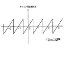
ここで、このように求めた自己相関関数(Corr(t))は上記の式に示すように複素信号であり、その位相成分は、キャリア周波数誤差に比例している。従って、狭帯域fc誤差算出回路108は、このようなOFDMシンボルの境界部分での自己相関値を求め、この自己相関値における位相をキャリア周波数誤差として出力する。もっとも、この自己相関関数から求められるキャリア周波数誤差は、図8に示すように、サブキャリア周波数間隔で鋸状に繰り返されるものであるので、検出範囲はサブキャリア周波数間隔の±1/2以下の精度の情報となる。このように狭帯域fc誤差算出回路108で求められた狭帯域のキャリア周波数誤差の情報は、狭帯域キャリア周波数誤差信号としてNCO110に供給される。
【0029】
また、この狭帯域fc誤差算出回路108で算出されたピーク位置の情報は、上述したようにOFDMシンボルの境界を示している。狭帯域fc誤差算出回路108により求められたOFDMシンボルの境界情報は、FFTウィンドウ同期回路111に供給され、FFTウィンドウの同期に用いられる。
【0030】
つぎに、広帯域fc誤差算出回路109について説明する。
【0031】
まず、広帯域fc誤差算出回路109によるキャリア周波数誤差の算出原理について説明する。
【0032】
OFDM信号には、一般に、CP(Continual Pilots)信号と呼ばれるパイロット信号が含まれている。このCP信号は、特定の位相及び振幅を常に表している信号であり、有効シンボル内の複数のインデックスのサブキャリアに挿入されている。有効シンボル内に含まれるCP信号の数、及び、その挿入位置の配置パターンは、予め規格により定められている。例えば、DVB−T規格(2Kモード)であれば、1つの有効シンボル内に2048本のサブキャリア(0〜2047)が存在するが、そのうち45本のサブキャリアにCP信号が含まれている。また、このDVB−T規格(2Kモード)においては、CP信号の配置パターンが、サブキャリアのインデックス番号(信号が変調されている1705本の範囲内)で、0、48、54、87、141、156、192、201、255、279、282、333、432、450、483、525、531、618、636、714、759、765、780、804、873、888、918、939、942、969、984、1050、1101、1107、1110、1137、1140、1146、1206、1269、1323、1377、1491、1683、1704となっている。
【0033】
広帯域fc誤差算出回路109は、FFT演算後のOFDM周波数領域信号に対して、時間的に前後したシンボル間で2回の差動復調を行うことによってCP信号を抽出し、抽出したCP信号のサブキャリア位置が、本来のサブキャリア位置からどの程度シフトしているかを算出することによって、OFDM信号のキャリア周波数誤差を算出している。
【0034】
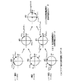
OFDM周波数領域信号に対して2回のシンボル間の差動復調を行うことよって、CP信号を抽出することができる原理を図9を用いて説明する。
【0035】
図9は、1段階目のシンボル間の差動復調、及び、2段階目のシンボル間の差動復調について説明するための通常の情報データとCP信号との位相変遷を説明する図である。なお、この図9において、情報データはQPSK(Quadrature Phase Shift Keying)変調されているものとし、また、CP信号には、ある特定の振幅及び位相の信号点の情報が変調されているものとする。
【0036】
図9(A)は、FFTにより各サブキャリアの周波数成分毎に分解されたIチャンネル信号及びQチャンネル信号を、シンボル毎(n−1番目のシンボル、n番目のシンボル、n+1番目のシンボル)に位相平面上に示したものである。an,bnは第n番目のOFDMシンボルのFFT後のサブキャリアのインデックス番号がa,bである情報データをそれぞれ示しており、また、can,cbnは第n番目のOFDMシンボルのFFT後のサブキャリアのインデックス番号がca,cbであるCP信号をそれぞれ示している。なお、CP信号は、本来、一定の振幅および位相情報を有しているが、再生搬送波周波数誤差等の影響により、シンボル毎に多少の位相回転を生じている場合がある。
【0037】
また、図9(B)は、同一のインデックス番号の情報をシンボル間の一回の差動復調をとったときの一回差動復調データを位相平面上に示したものである。dan,dbnはそれぞれサブキャリアのインデックス番号がa,bである第(n−1)番目のシンボルと第n番目のシンボルとの一回差動復調データである。また、dcan、dcbnはそれぞれサブキャリアのインデックス番号がca,cbである第(n−1)番目のシンボルと第n番目のシンボルとの一回差動復調データである。
【0038】
また、図9(C)は、同一のインデックス番号の情報をシンボル間で二回の差動復調をとったときの二回差動復調データを位相平面上に示したものである。dda,ddbは、それぞれサブキャリアのインデックス番号がa,bである第(n−1)番目のシンボルと第n番目シンボルを差動復調したものと、第n番目のシンボルと第(n+1)番目のシンボルとを差動復調したものとを、更に、差動復調した結果得られる二回差動復調データである。また、ddca,ddcbは、それぞれサブキャリアのインデックス番号がca,cbの第(n−1)番目のシンボルと第n番目シンボルを差動復調したものと、第n番目のシンボルと第(n+1)番目シンボルを差動復調したものとを更に差動復調した結果得られる二回差動復調データである。
【0039】
CP信号ca,cbは、一定位相の信号であることから、一回目の差動復調ではFFT窓位相誤差、キャリア位相誤差が除外され、キャリア周波数誤差、CPE、及び、再生クロック周波数誤差に依存した位相誤差が残ることとなる。この一回目の差動復調後に残った位相誤差はいずれも時間に依存しないため、差動復調後のデータ間で一定となる。そこで、さらに二回目の差動復調を一回目の差動復調が施されたデータの間で行うことで、一回目の差動復調で残ったCPE及び再生クロック周波数に依存した位相誤差を取り除くことができる。その結果、CP信号はI軸上の正のある値に収束する(図9(C)参照)。
【0040】
それに対して、情報データa,bはシンボル間でランダムな位相を取るために、二回の差動復調を行った後もその位相はデータ毎にランダムになり、その結果、そのデータはI軸上にランダムに分散する。
【0041】
従って、例えば、1シンボル内においてCP信号のI軸データのみ累積加算等をすると、このCP信号はI軸上のある値に収束しているため、情報データのみが取り出されたI軸データを累積加算した結果に比べて遥かに大きい値となる。そのため、この累積加算の最大値からCP信号のサブキャリア位置を推定することができる。そして、推定されたCP信号のサブキャリア位置が、本来のサブキャリアの配置位置からどの程度シフトしているかを算出することにより、キャリア周波数誤差をサブキャリア間隔精度で算出することができる。
【0042】
つぎに、広帯域fc誤差算出回路109の具体的な回路例について説明する。
【0043】
図10に広帯域fc誤差算出回路109のブロック構成図を示す。
【0044】
広帯域fc誤差算出回路109は、第1の差動復調回路121と、第2の差動復調回路122と、メモリ123と、パイロット信号選択データ発生回路124と、制御回路125と、累積加算回路126と、最大値検出回路127と、キャリア周波数誤差記憶回路128と、ゲート回路129とを有している。
【0045】
第1の差動復調回路121及び第2の差動復調回路122は、それぞれ第1及び第2のファーストインファーストアウトメモリ(FIFO)131,132と、符号反転回路133と、複素乗算回路134とから構成されている。
【0046】
第1の差動復調回路121には、FFT演算回路107から出力されるOFDM周波数領域信号(Iチャンネル信号,Qチャンネル信号)が供給される。第1のFIFO131にはIチャンネル信号が供給され、第2のFIFOにはQチャンネル信号が供給される。第1及び第2のFIFO131,132は、1有効シンボル分のOFDM周波数領域信号を格納するだけのメモリ容量を有しており、供給されたIチャンネル信号,Qチャンネル信号を1有効シンボル分遅延させる。符号反転回路133は、第2のFIFO132により遅延されたQチャンネル信号を符号反転させる。複素乗算回路134には、FFT演算回路107から出力されたOFDM周波数領域信号(Iチャンネル信号,Qチャンネル信号)と、第1及び第2のFIFO131,132により1有効シンボル分遅延されたOFDM周波数領域信号(Iチャンネル信号,Qチャンネル信号)とが入力される。この複素乗算回路134は、遅延されていないOFDM周波数領域信号と、遅延されたOFDM周波数領域信号との複素乗算を行って差動復調を行い、OFDM周波数領域信号のシンボル間の一回差動復調データを求める。具体的に、第1の差動復調回路121は、遅延されていないIチャンネルデータとQチャンネルデータをI,Qと表し、遅延されたIチャンネルデータとQチャンネルデータをそれぞれI-1,Q-1と表すと、以下に示す複素演算を行う。
(I+jQ)(I-1−jQ-1)
そして、第1の差動復調回路121は、この演算結果を実数成分と虚数成分とに分けて第2の差動復調回路122に出力する。
【0047】
第2の差動復調回路122は、上記第1の差動復調回路121と同一の構成となっており、第1の差動復調回路121から出力されたシンボル間の一回差動復調データに対して、再度差動復調を行って、シンボル間の二回差動復調データを求める。なお、第2の差動復調回路122は、複素乗算結果のI軸成分(実数成分)のみを出力する。第2の差動復調回路122は、シンボル間の二回差動復調データをメモリ123に供給する。
【0048】
メモリ123は、第2の差動復調回路122から出力される1シンボル分のシンボル間の二回差動復調データを、例えばサブキャリアのインデックス番号順に格納する。メモリ123は、パイロット信号選択データ発生回路124から与えられる読み出しアドレスに従い、格納しているデータのうちアドレスで指定されたデータのみを累積加算回路126に供給する。
【0049】
パイロット信号選択データ発生回路124は、メモリ123に格納されている二回差動復調データ(I成分)のうち、CP信号を特定するためのアドレス情報を発生する。具体的には、パイロット信号選択データ発生回路124は、1つの有効シンボルを構成する複数のサブキャリア(例えば2048本のサブキャリア)の中から、CP信号が変調されている複数のサブキャリア(例えば45本のサブキャリア)の配置位置を特定するインデックス番号の集合データを保持しており、このインデックス番号の集合データをメモリ123の読み出しアドレスとして発生する。そして、この読み出しアドレスとして指定されたデータが、累積加算回路126に供給される。具体的には、この読み出しアドレスで特定される45個のデータがメモリ123から読み出され、累積加算回路126に供給される。なお、メモリ123に対して読み出しアドレスとして供給するCP信号のインデックス番号を特定する集合データのことをCP信号選択データと呼ぶ。また、このパイロット信号選択データ発生回路124は、制御回路125から供給されるシフト量feに応じて、そのCP信号選択データを適宜シフトさせて(CP信号選択データを構成する各値に対して一律に一定の値を加算または減算して)、メモリ123に対して複数回読み出しアドレスを与えて、メモリ123から複数回のデータの読み出しを行う。
【0050】
パイロット信号選択データ発生回路124から発生されるCP信号選択データのデータ例を図11を用いて説明する。なお、具体的に説明するために、制御回路125からfe=−10〜+10のシフト量が供給されるものとするが、シフト量feの供給数はどのような数としてもよい。制御回路125からシフト量fe=0が供給されると、パイロット信号選択データ発生回路124は、図11(D)に示すようなCP信号選択データを発生して、メモリ123に供給する。シフト量fe=0の時に発生されるCP信号選択データは、規格上定められている本来CP信号が変調されているサブキャリアのインデックス番号を示したデータ群である。
【0051】
また、シフト量fe=Δfが供給されると、パイロット信号選択データ発生回路124は、図11(E)に示すようなCP信号選択データを発生して、メモリ123に供給する。このシフト量fe=Δfの時に発生されるCP信号選択データは、本来CP信号が変調されているサブキャリアのすべてのインデックス番号に1を加算したデータ群である。また、シフト量fe=2Δfが供給されると、パイロット信号選択データ発生回路124は、図11(F)に示すような本来CP信号が変調されているサブキャリアのすべてのインデックス番号に2を加算したデータ群を発生する。同様に、シフト量fe=3Δf〜9Δfが供給されると、本来CP信号が変調されているサブキャリアのすべてのインデックス番号にシフト量Δfを加算したデータ群を発生し、シフト量fe=10Δfが供給されると、パイロット信号選択データ発生回路124は、図11(G)に示すような本来CP信号が変調されているサブキャリアのすべてのインデックス番号に10を加算したデータ群を発生する。
【0052】
一方、マイナスのシフト量fe=−Δfが供給されると、パイロット信号選択データ発生回路124は、図11(A),図11(B),図11(C)に示すような本来CP信号が変調されているサブキャリアのすべてのインデックス番号にシフト量Δfを減算したデータ群を発生する。なお、インデックス番号の値が0以下となった場合には、有効シンボルのサブキャリアのインデックス番号(0〜2047)をサイクリックに繰り返すように、2047の値に戻っていく。
【0053】
このようなメモリ123へ読み出しアドレスとして供給するCP信号選択データは、メモリ123に格納される二回差動復調データが更新されるまでの間に、例えば図11に示したような21パターンのCP信号選択データが、順次発生される。即ち、1シンボル期間の間に、−10Δf〜10Δfのシフト量が順次パイロット信号選択データ発生回路124に供給され、それに伴い、それぞれのシフト量feに対応した45個のデータが、例えば21回順次に累積加算回路126に供給される。
【0054】
累積加算回路126は、CP信号選択データにより選択された複数の二回差動復調データが供給され、それらの二回差動復調データを累積加算する。すなわち、CP信号選択データにより選択された45個の値をすべて累積加算する。この累積加算回路126は、CP信号選択データがメモリ123に供給されるタイミングと同期してリセットされる。すなわち、1シンボル期間内に図11に示したような21パターンのCP信号選択データが供給される場合には、各パターンで選択された二回差動復調データが供給される毎にリセットされる。従って、累積加算回路126は、1シンボル期間内に、例えば21個の累積加算結果を、1つずつ順次出力していくこととなる。この累積加算回路126からの出力結果は、最大値検出回路127に供給される。
【0055】
最大値検出回路127は、セレクタ135と、RAM136と、比較回路137とを備え、累積加算回路126から出力される例えば21個の累積加算結果のうち、最大の累積加算結果を選択し、最大の累積加算結果が選択されたタイミングで、イネーブル信号を出力する。具体的には、比較回路137がRAM136に格納されている値と、累積加算回路126から供給された累積加算結果とを比較し、RAM136に格納されている値よりも累積加算回路126から供給された累積加算結果の方が大きい場合には、イネーブル信号を出力する。このイネーブル信号は、セレクタ135に供給される。セレクタ135は、イネーブル信号が供給されると、その累積加算結果をRAM136に格納する。従って、RAM136には、累積加算回路126から供給される例えば21個の累積加算結果のうち、最大の累積加算結果が格納されることとなり、また、比較回路127から出力されるイネーブル信号は、例えば21個の累積加算結果のうち最大の累積加算結果を選択したときが最後(1シンボル期間内での最後)の発生タイミングとなる。なお、最大値検出回路127のRAM136は、1シンボル期間毎(メモリ123内の二回差動復調データが更新されるタイミング)に内部データがクリアされる。
【0056】
キャリア周波数誤差記憶回路128は、セレクタ138と、セレクタ138により選択されたデータを格納するRAM139とから構成される。セレクタ138には、制御回路125からパイロット信号選択データ発生回路124に供給するシフト量feが、パイロット信号選択データ発生回路124に供給するタイミングに同期して供給される。それとともに、セレクタ138には、後段に接続されているRAM139の出力がフィードバックして入力されている。セレクタ135は、最大値検出回路127の比較回路137から出力されるイネーブル信号に従い動作する。具体的には、イネーブル信号が供給されたときには、制御回路138から供給されたシフト量feをRAM139に格納し、イネーブル信号が供給されなかったときには、RAM139からフィードバックされたシフト量feをRAM139に格納する。このことにより、RAM139には、CP信号の累積加算結果が最大値となるCP信号選択データのシフト量feが、RAM139に格納されることとなる。
【0057】
そして、ゲート回路129は、1シンボル期間毎のタイミングで、RAM139に格納されているシフト量feをラッチし、その値をサブキャリア間隔毎のキャリア誤差値として出力する。
【0058】
以上のように処理を行うことによって、広帯域fc誤差算出回路109は、FFT演算後のOFDM周波数領域信号に対して、有効シンボル内に含まれている複数のCP信号を抽出し、抽出したそのCP信号のサブキャリア位置が、本来のサブキャリア位置からどの程度シフトしているかを算出することができ、OFDM信号のキャリア周波数誤差をサブキャリア間隔精度で算出することができる。
【0059】
つぎに、CPEキャンセル回路112及びCPE算出回路113について図12を用いて説明する。
【0060】
CPEキャンセル回路112は、図12に示すように、1シンボル遅延回路141と、複素乗算回路142とを備えている。また、CPE算出回路113は、差動復調回路151と、CP選択回路152と、平均化回路153と、Tan-1回路154と、累積加算回路155と、複素変換回路156とを備えている。
【0061】
差動復調回路151は、FFT演算回路107から出力されたOFDM周波数領域信号に対して、シンボル間の差動復調データを求める。この差動復調回路151の回路構成は、上述した広帯域fc誤差算出回路109の第1の差動復調回路121と同一の回路構成となる。差動復調回路151は、算出したシンボル間の差動復調データをCP選択回路152に供給する。
【0062】
CP選択回路152は、供給されたシンボル間の一回差動復調データのうち、CP信号成分の一回差動復調データを抽出する。CP信号は、上述したように有効シンボル内の複数のサブキャリアのうち、予め定められた位置に複数含まれている。例えば、DVB−T規格(2Kモード)においては、1シンボル内に45個のCP信号が含まれている。CP選択回路152は、例えば、CP信号が変調されているサブキャリアのインデックスを記憶しておき、そのインデックスのデータのみを抜き出すことによって、CP信号を選択する。CP信号成分のシンボル間の一回差動復調データは、平均化回路153に供給される。
【0063】
平均化回路153は、CP信号のシンボル間の一回差動復調データを、1シンボル内で平均化する。平均化回路153は、例えば45個のCP信号の一回差動復調データの1シンボル内における平均値を求め、その値をシンボル内の位相変動量として出力する。この位相変動量は、Tan-1回路153に供給される。
【0064】
Tan-1回路153は、複素信号として供給される位相変動量に対して、実数成分と虚数成分とのアークタンジェントを演算することにより、位相変動量の角度データを求める。求められた位相変動量の角度データは、累積加算回路155に供給される。
【0065】
累積加算回路155は、供給された角度データを累積加算する。1シンボル毎の位相変動成分を累積加算することによって、OFDM信号の位相変動に追従していくことが可能となる。累積加算された角度データは、複素変換回路156に供給される。
【0066】
複素変換回路156は、角度データを実数成分(I成分)と虚数成分(Q成分)とからなる複素信号に変換する。複素信号に変換された位相変動量は、CPE補正信号として、CPEキャンセル回路112の複素乗算回路112に供給される。
【0067】
一方、FFT演算回路107から出力されたOFDM周波数領域信号は、CPEキャンセル回路112の1シンボル遅延回路141により1シンボル分遅延された後、CPEキャンセル回路112の複素乗算回路142に供給される。ここで、1シンボル分遅延されるのは、CPE算出回路113によりCPE補正信号を求める際に、差動復調を行うので、1シンボル分処理が遅延するためである。
【0068】
複素乗算回路142は、1シンボル分遅延されたOFDM周波数領域信号と、CPE算出回路113の複素変換回路156から供給された位相変動量とを複素乗算して、OFDM周波数領域信号に含まれているCPE成分を除去する。
【0069】
【発明が解決しようとする課題】
以上のように従来のOFDM受信装置では、FFT演算後の周波数領域信号からCP信号を抽出し、このCP信号のシフト量からOFDM信号の広帯域のキャリア周波数誤差を検出していた。具体的には、CP信号の位相成分が0であることを利用し、FFT復調後の複素データに対して2回のシンボル間の差動復調を行い、2回のシンボル間の差動復調を検出した結果が0となる信号をCP信号として抽出していた。
【0070】
しかしながら、伝送経路や受信状態が悪化してCP信号が減衰した場合、CP信号のエネルギーよりもノイズエネルギーが大きくなり、CP信号以外の信号をCP信号であるものと誤って検出してしまう可能性がある。このようにCP信号以外の信号をCP信号であると誤って検出すると、キャリア周波数誤差が変動し、キャリア周波数補正の同期がはずれてしまう。
【0071】
本発明は、以上のような問題を解決し、OFDM信号のキャリア周波数補正制御動作の同期を安定的に保持することが可能な復調装置及び復調方法を提供することを目的とする。
【0072】
【課題を解決するための手段】
本発明にかかる復調装置は、直交周波数分割多重(OFDM)信号を復調する復調装置であって、位相成分が同一とされたパイロット信号がシンボル内の所定のサブキャリア位置に直交変調されたOFDM信号とキャリア周波数誤差補正信号とを複素乗算して、上記OFDM信号のキャリア周波数を補正するキャリア周波数補正手段と、上記キャリア周波数補正手段によりキャリア周波数が補正された上記OFDM信号を、1シンボル期間単位でフーリエ変換して各サブキャリアに変調されている情報を復調し、周波数領域信号を生成するフーリエ変換手段と、上記フーリエ変換手段により復調された上記周波数領域信号から上記パイロット信号を検出し、上記パイロット信号に基づき、上記OFDM信号のキャリア周波数誤差を算出するとともに、上記パイロット信号の角度成分をシンボル間で2回差動復調した実数成分を1シンボル内で累積加算した累積加算値を算出するキャリア周波数誤差算出手段と、上記キャリア周波数誤差算出手段により算出された上記OFDM信号のキャリア周波数誤差に基づき、上記周波数誤差補正信号を生成する周波数誤差補正信号生成手段と、上記キャリア周波数誤差算出手段により算出されたキャリア周波数誤差が変動したときに、上記累積加算値が所定の閾値以下である場合には、上記キャリア周波数誤差算出手段から出力されるキャリア周波数誤差を変動前の値にホールドするホールド手段とを備える。
【0074】
本発明にかかる復調方法は、直交周波数分割多重(OFDM)信号を復調する復調方法であって、位相成分が同一とされたパイロット信号がシンボル内の所定のサブキャリア位置に直交変調されたOFDM信号を1シンボル期間単位でフーリエ変換することによって各サブキャリアに変調されている情報を復調して周波数領域信号を生成し、上記周波数領域信号から上記パイロット信号を検出し、上記パイロット信号に基づき、上記OFDM信号のキャリア周波数誤差を算出するとともに、上記パイロット信号の角度成分をシンボル間で2回差動復調した実数成分を1シンボル内で累積加算した累積加算値を算出し、算出された上記OFDM信号のキャリア周波数誤差に基づき、周波数誤差補正信号を生成し、上記キャリア周波数誤差補正信号と上記OFDM信号とを複素乗算して、上記OFDM信号のキャリア周波数を補正し、算出された上記キャリア周波数誤差が変動したときに、上記累積加算値が所定の閾値以下である場合には、上記キャリア周波数誤差を変動前の値にホールドする。
【0076】
【発明の実施の形態】
以下、本発明の実施の形態として、本発明を適用したOFDM方式によるデジタル放送の受信装置(OFDM受信装置)について説明する。
【0077】
図1に本発明を適用したOFDM受信装置のブロック構成図を示す。なお、図1では、ブロック間で伝達される信号が複素信号の場合には太線で信号成分を表現し、ブロック間で伝達される信号が実数信号の場合には細線で信号成分を表現している。
【0078】
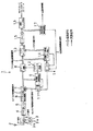
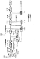
OFDM受信装置1は、この図1に示すように、アンテナ2と、チューナ3と、バンドパスフィルタ(BPF)4と、A/D変換回路5と、デジタル直交復調回路6と、fc補正回路7と、FFT演算回路8と、狭帯域fc誤差算出回路9と、広帯域fc誤差・CPE算出回路10と、数値コントロール発振回路(NCO)11と、FFTウィンドウ同期回路12と、CPEキャンセル回路13と、ホールド回路14と、イコライザ15と、検波・エラー訂正回路16と、伝送制御情報復調回路17とを備えている。
【0079】
放送局から放送されたデジタルテレビジョン放送の放送波は、OFDM受信装置1のアンテナ2により受信され、RF信号としてチューナ3に供給される。
【0080】
アンテナ2により受信されたRF信号は、局部発振器3a及び乗算器3bからなるチューナ3によりIF信号に周波数変換され、BPF4に供給される。IF信号は、BPF4によりフィルタリングされた後、A/D変換回路5によりデジタル化され、デジタル直交復調回路6に供給される。A/D変換回路5は、例えば、DVB−T規格においては、有効シンボルのサンプリング数が2048サンプルでサンプリングできるようなクロックで、即ち、1OFDMシンボルを2560(2048+512)サンプルでサンプリングできるようなクロックでサンプリングを行う。
【0081】
デジタル直交復調回路6は、所定の周波数(fc:キャリア周波数)のキャリア信号を用いて、デジタル化されたIF信号を直交復調し、ベースバンドのOFDM信号を出力する。このデジタル直交復調回路6から出力されるベースバンドのOFDM信号は、FFT(Fast Fourier Transferorm)演算される前のいわゆる時間領域の信号であることから、以下OFDM時間領域信号と呼ぶ。このOFDM時間領域信号は、直交復調された結果、実軸成分(Iチャンネル信号)と、虚軸成分(Qチャネル信号)とを含んだ複素信号となっている。デジタル直交復調回路6により出力されるOFDM時間領域信号は、fc補正回路7に供給される。
【0082】
fc補正回路7は、NCO11から出力されたキャリア周波数誤差補正信号とOFDM時間領域信号と複素乗算し、OFDM時間領域信号のキャリア周波数誤差を補正する。キャリア周波数誤差は、例えば局部発振器102aから出力される基準周波数のずれ等により生じるOFDM時間領域信号の中心周波数位置の誤差であり、この誤差が大きくなると出力されるデータの誤り率が増大してしまう。fc補正回路7によりキャリア周波数誤差が補正されたOFDM時間領域信号は、FFT演算回路8及び狭帯域fc誤差算出回路9に供給される。
【0083】
FFT演算回路8は、OFDM時間領域信号に対してFFT演算を行い、各サブキャリアに対して変調されているデータを抽出して出力する。このFFT演算回路8から出力される信号は、FFTされた後のいわゆる周波数領域の信号であることから、以下、OFDM周波数領域信号と呼ぶ。
【0084】
FFT演算回路8は、OFDMシンボルからガードインターバルの時間長分の信号を除去することにより得られる有効シンボル長の範囲(2048サンプルの範囲)に対してFFT演算を行う。その演算範囲(FFTウィンドウ)がFFTウィンドウ同期回路12により制御される。具体的にその演算開始位置は、OFDMシンボルの境界から、ガードインターバルの終了位置までの間のいずれかの位置となる。
【0085】
このようにFFT演算回路8から出力されたOFDM周波数領域信号は、OFDM時間領域信号と同様に、実軸成分(Iチャンネル信号)と、虚軸成分(Qチャネル信号)とからなる複素信号となっている。OFDM周波数領域信号は、広帯域fc誤差・CPE算出回路10、CPEキャンセル回路13に供給される。
【0086】
狭帯域fc誤差算出回路9は、デジタル直交復調回路6によりデジタル直交復調した後のOFDM時間領域信号に含まれる狭帯域のキャリア周波数誤差を算出する。具体的に、狭帯域fc誤差算出回路9は、サブキャリアの周波数間隔(例えば4.464kHz)の±1/2以下の精度でキャリア周波数誤差を算出する。狭帯域fc誤差算出回路9により求められた狭帯域キャリア周波数誤差は、NCO11に供給される。なお、この狭帯域fc誤差算出回路9による狭帯域キャリア周波数誤差の算出方法は、従来例において説明したものと同様である。
【0087】
広帯域fc誤差・CPE算出回路10は、デジタル直交復調回路6によりデジタル直交復調した後のOFDM時間領域信号に含まれるキャリア周波数誤差を算出する。具体的に、広帯域fc誤差・CPE算出回路10は、サブキャリアの周波数(例えば4.464kHz)間隔精度の広帯域キャリア周波数誤差を算出する。広帯域fc誤差・CPE算出回路10により求められた広帯域キャリア周波数誤差は、ホールド回路14を介してNCO11に供給される。また、広帯域fc誤差・CPE算出回路10は、OFDM時間領域信号に含まれるCPE(Common Phase Error)を検出し、このCPEを補正するためのCPE補正信号生成し、CPEキャンセル回路13に供給する。なお、この広帯域fc誤差・CPE算出回路10の具体的な内容については、その詳細を後述する。
【0088】
NCO11は、狭帯域fc誤差算出回路9により算出されたサブキャリア周波数間隔の±1/2以下の精度の狭帯域キャリア周波数誤差と、広帯域fc誤差・CPE算出回路10により算出されたサブキャリア周波数間隔精度の広帯域キャリア周波数誤差とを加算し、加算して得られたキャリア周波数誤差に応じて周波数が増減するキャリア周波数誤差補正信号を出力する。このキャリア周波数誤差補正信号は、複素信号であり、fc補正回路7に供給される。このキャリア周波数誤差補正信号は、fc補正回路7によりOFDM時間領域信号に複素乗算され、OFDM時間領域信号のキャリア周波数誤差成分は除去される。
【0089】
FFTウィンドウ同期回路12は、狭帯域fc誤差算出回路9がサブキャリアの周波数間隔の±1/2以下の精度の狭帯域キャリア周波数誤差を算出する際に得られるOFDMシンボルの境界位置情報に基づき、FFT演算回路8によるFFT演算の開始タイミングを求め、FFT演算を行う範囲(FFTウィンドウ)を制御する。
【0090】
CPEキャンセル回路13は、OFDM周波数領域信号に対して広帯域fc誤差・CPE算出回路10により算出されたCPE補正信号を複素乗算することによって、OFDM周波数領域信号に含まれているCPE(Common Phase Error)の除去を行う。
【0091】
イコライザ15は、スキャッタードパイロット信号(SP信号)を用いて、OFDM周波数領域信号の位相等化及び振幅等化を行う。位相等化及び振幅等化がされたOFDM周波数領域信号は、検波・エラー訂正回路16に供給される。
【0092】
検波・エラー訂正回路16は、各サブキャリアに変調されている情報をその変調方式に応じて検波し、デマッピング等を行ってデータを復号する。その後、検波・エラー訂正回路16は、復号したデータに対してエラー訂正処理を行って、例えば、MPEG−2トランスポートストリームを出力する。
【0093】
伝送制御情報復調回路17は、所定のサキャリア位置に変調されているTMCC(Transmission and Multiplexing Configuration Control)やTPS(Transmission Parameter Signaling)といった伝送制御情報を復調する。復調された伝送制御情報は、例えば、図示しないシステムコントローラ等に供給され、復調や再生の制御に用いられる。また、伝送制御情報復調回路17は、伝送制御情報を検出できているか否かを示す伝送制御情報検出信号を、ホールド回路14に供給する。
【0094】
つぎに、広帯域fc誤差・CPE算出回路10について説明する。
【0095】
まず、広帯域fc誤差・CPE算出回路10による広帯域キャリア周波数誤差の算出原理について説明する。
【0096】
OFDM信号には、CP(Continual Pilots)信号と呼ばれるパイロット信号が含まれている。このCP信号は、特定の位相及び振幅を常に表している信号であり、有効シンボル内の複数のインデックスのサブキャリアに挿入されている。有効シンボル内に含まれるCP信号の数、及び、その挿入位置の配置パターンは、予め規格により定められている。例えば、DVB−T規格(2Kモード)であれば、1つの有効シンボル内に2048本のサブキャリア(0〜2047)が存在するが、そのうち45本のサブキャリアにCP信号が含まれている。CP信号が挿入されている具体的なサブキャリアのインデックス番号は、従来例において説明したとおりである。
【0097】
この広帯域fc誤差・CPE算出回路10は、FFT演算後のOFDM周波数領域信号を角度データに変換した後、この角度データに対して時間的に前後したシンボル間で2回の差分検出を行うことによってCP信号を抽出し、抽出したCP信号のサブキャリア位置が、本来のサブキャリア位置からどの程度シフトしているかを算出することによって、OFDM信号の広帯域キャリア周波数誤差を算出している。
【0098】
また、広帯域fc誤差・CPE算出回路10は、FFT演算後のOFDM周波数領域信号を角度データに変換した後、この角度データに対して時間的に前後したシンボル間で一回の差分検出を行い、CPEを算出している。
【0099】
広帯域fc誤差・CPE算出回路10の具体的な回路例について説明する。
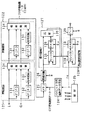
【0100】
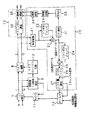
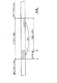
図2に広帯域fc誤差・CPE算出回路10のブロック構成図を示す。
【0101】
広帯域fc誤差・CPE算出回路10は、角度変換回路21と、第1の1シンボルディレイ回路22と、第1の減算回路23と、第2の1シンボルディレイ回路24と、第2の減算回路25と、コサイン回路26と、シフト量演算回路27と、CP選択回路31と、平均化回路32と、累積加算回路33と、複素演算回路34とから構成される。
【0102】
角度変換回路21には、FFT演算回路8からOFDM周波数領域信号が供給される。角度変換回路21は、複素信号として供給されるOFDM周波数領域信号に対して、実数成分と虚数成分とのアークタンジェントを演算することにより、OFDM周波数領域信号を角度データに変換する。求められた角度データは、第1の1シンボルディレイ回路22及び第1の減算回路23に供給される。
【0103】
第1の1シンボルディレイ回路22は、例えばFIFO等からなり、角度変換回路21により角度データとされたOFDM周波数領域信号を、1シンボル分遅延させ、第1の減算回路23に供給する。この第1の1シンボルディレイ回路22は、1有効シンボル分の角度信号を格納するだけのメモリ容量(2048サンプル分の容量)を有していればよい。
【0104】
第1の減算回路23は、例えば単純な加算回路等からなり、1シンボル分遅延させた角度データと、遅延されていない角度データとの差分演算を行う。ここで、角度データの一回のシンボル間の差分を演算すると、通常の情報データは、シンボル間でランダムな角度を取るために、角度の差分をとった後の角度がデータ毎にランダムとなる。それに対して、CP信号は、もともと全て一定位相の信号であることから、一回の角度の差分をとると、本来の信号成分が除去される。それとともに、FFT窓位相誤差及びキャリア位相誤差が除去される。CP信号に対して一回のシンボル間の角度の差分を取ることにより残っている情報は、キャリア周波数誤差、CPE及び再生クロック周波数誤差に依存した位相誤差となる。
【0105】
第1の減算回路23は、演算結果を、一回差分データとして、第2の減算回路25、第2の1シンボルディレイ回路24及びCP選択回路31に供給する。
【0106】
第2の1シンボルディレイ回路24は、第1の1シンボルディレイ回路22と同様に、例えば、FIFO等からなり、第1の減算回路23から供給される一回差分データを、1シンボル分遅延させ、第2の減算回路24に供給する。この第2の1シンボルディレイ回路24も、1有効シンボル分の一回差分データを格納するだけのメモリ容量を有していればよい。
【0107】
第2の減算回路25は、第1の減算回路23と同様に、例えば単純な加算回路等からなり、1シンボル分遅延させた一回差分データと、遅延されていない一回差分データとの差分演算を行う。この第2の減算回路25により差分演算がされると、結果として、角度データとされたOFDM周波数領域信号を、シンボル間で2回差分をとったこととなる。ここで、角度データの2回のシンボル間の差分を演算すると、通常の情報データは、シンボル間でランダムな角度を取るため、一回のシンボル間の差分をとったときと同様に、角度がデータ毎にランダムとなる。それに対して、CP信号は、二回の角度の差分をとると、CPE及び再生クロック周波数誤差に依存した位相誤差が除去され、キャリア周波数誤差が残ることとなる。そして、一回目の角度差分演算後に残った誤差は時間に依存しない情報のため、さらに二回目の角度差分演算を行うことで、CP信号は、0の値に収束することととなる。
【0108】
第2の減算回路25は、演算結果である二回差分データとして、コサイン回路26に供給する。
【0109】
コサイン回路26は、供給された二回差分データに対してコサイン演算を行うことによって、角度成分を、複素信号の実数成分(即ち、Iチャネル信号)に変換する。そのため、Iチャンネル信号に変換された二回差分データは、情報データ成分がI軸上にランダムに分布するのに対して、CP信号成分は、I軸上の1の値に収束することとなる。コサイン回路26は、Iチャンネル信号に変換した二回差分データを、シフト量算出回路27に供給する。
【0110】
シフト量算出回路27は、供給された二回差分データからCP信号を抽出してCP信号のサブキャリア位置を算出し、OFDM周波数領域信号に含まれているCP信号が本来配置されているサブキャリア位置からどの程度シフトしているかを、サブキャリア周波数間隔精度で算出する。
【0111】
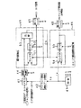
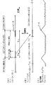
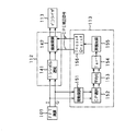
具体的に、シフト量算出回路27の回路例を図3に示す。
【0112】
シフト量算出回路27は、図3に示すように、メモリ41と、パイロット信号選択データ発生回路42と、制御回路43と、累積加算回路44と、最大値検出回路45と、キャリア周波数誤差記憶回路46と、第1のラッチ回路47と、第2のラッチ回路48とを有している。
【0113】
メモリ41は、コサイン回路26から出力される1シンボル分のシンボル間の二回差分データ(Iチャンネル信号)を、例えばサブキャリアのインデックス順に格納する。メモリ41は、パイロット信号選択データ発生回路42から与えられる読み出しアドレスに従い、格納しているデータのうちアドレスで指定されたデータのみを累積加算回路44に供給する。
【0114】
パイロット信号選択データ発生回路42は、メモリ41に格納されている二回差分データ(Iチャンネル信号)のうち、CP(Continual Pilots)信号を特定するためのアドレス情報を発生する。具体的には、パイロット信号選択データ発生回路42は、1つの有効シンボルを構成する複数のサブキャリア(例えば2048本のサブキャリア)の中から、CP信号が変調されている複数のサブキャリア(例えば45本のサブキャリア)の配置位置を特定するインデックスの集合データを保持しており、このインデックスの集合データをメモリ41の読み出しアドレスとして発生する。そして、この読み出しアドレスとして指定されたデータが、累積加算回路44に供給される。具体的には、この読み出しアドレスで特定される45個のデータがメモリ41から読み出され、累積加算回路44に供給される。なお、メモリ41に対して読み出しアドレスとして供給するCP信号のインデックスを特定する集合データのことをCP信号選択データと呼ぶ。また、このパイロット信号選択データ発生回路42は、制御回路43から供給されるシフト量feに応じて、そのCP信号選択データを適宜シフトさせて(CP信号選択データを構成する各値に対して一律に一定の値を加算または減算して)、メモリ41に対して複数回読み出しアドレスを与えて、メモリ41から複数回のデータの読み出しを行う。
【0115】
パイロット信号選択データ発生回路42から発生されるCP信号選択データは、従来例において図11を用いて説明したものと同様のものを用いる。
【0116】
このようなメモリ41へ読み出しアドレスとして供給するCP信号選択データは、メモリ41に格納される二回差分データが更新されるまでの間に、例えば図11に示したような21パターンのCP信号選択データが、順次発生される。即ち、1シンボル期間の間に、−10Δf〜10Δfのシフト量が順次パイロット信号選択データ発生回路42に供給され、それに伴い、それぞれのシフト量feに対応した45個のデータが、例えば21回順次に累積加算回路44に供給される。
【0117】
累積加算回路44は、CP信号選択データにより選択された複数の二回差分データが供給され、それらの二回差分データを累積加算する。すなわち、CP信号選択データにより選択された45個の値をすべて累積加算する。この累積加算回路44は、CP信号選択データがメモリ41に供給されるタイミングと同期してリセットされる。すなわち、1シンボル期間内に図11に示したような21パターンのCP信号選択データが供給される場合には、各パターンで選択された二回差分データが供給される毎にリセットされる。従って、累積加算回路44は、1シンボル期間内に、例えば21個の累積加算結果を、1つずつ順次出力していくこととなる。この累積加算回路44からの出力結果は、最大値検出回路45に供給される。
【0118】
最大値検出回路45は、セレクタ51と、RAM52と、比較回路53とを備え、累積加算回路44から出力される例えば21個の累積加算結果のうち、最大の累積加算結果(CP値累積加算結果)を選択し、最大の累積加算結果が選択されたタイミングで、イネーブル信号を出力する。最大の累積加算結果が得られた場合というのは、メモリ41からにより読み出されたデータが、CP信号であることを示している。即ち、CP信号は、その値が1に収束されており、それに対してその他の情報データは、ランダムな値となっている。従って、CP信号のみを抽出して累積加算すれば、その他の情報データを累積加算した結果よりもその累積加算値が高くなり、最大の累積加算結果を選択することによって、CP信号のシフト量を得ることができる。
【0119】
具体的には、比較回路53がRAM52に格納されている値と、累積加算回路44から供給された累積加算結果とを比較し、RAM52に格納されている値よりも累積加算回路44から供給された累積加算結果の方が大きい場合には、イネーブル信号を出力する。このイネーブル信号は、セレクタ51に供給される。セレクタ51は、イネーブル信号が供給されると、その累積加算結果をRAM52に格納する。従って、RAM52には、累積加算回路44から供給される例えば21個の累積加算結果のうち、最大の累積加算結果(CP値累積加算結果)が格納されることとなり、また、比較回路53から出力されるイネーブル信号は、例えば21個の累積加算結果のうち最大の累積加算結果を選択したときが最後(1シンボル期間内での最後)の発生タイミングとなる。なお、最大値検出回路45のRAM52は、1シンボル期間毎(メモリ41内の二回差分データが更新されるタイミング)に内部データがクリアされる。
【0120】
また、RAM52に格納された累積加算結果の最大値(CP値累積加算結果)は、第1のラッチ回路47に供給され、1シンボル毎のタイミングで第1のラッチ回路47からホールド回路14に供給される。
【0121】
キャリア周波数誤差記憶回路46は、セレクタ54と、セレクタ54により選択されたデータを格納するRAM55とから構成される。セレクタ54には、制御回路43からパイロット信号選択データ発生回路42に供給するシフト量feが、パイロット信号選択データ発生回路42に供給するタイミングに同期して供給される。それとともに、セレクタ54には、後段に接続されているRAM55の出力がフィードバックして入力されている。セレクタ54は、最大値検出回路45の比較回路53から出力されるイネーブル信号に従い動作する。具体的には、イネーブル信号が供給されたときには、制御回路43から供給されたシフト量feをRAM55に格納し、イネーブル信号が供給されなかったときには、RAM55からフィードバックされたシフト量feをRAM55に格納する。このことにより、RAM55には、CP信号の累積加算結果が最大値となるCP信号選択データのシフト量feが、RAM55に格納されることとなる。
【0122】
そして、第2のラッチ回路48は、1シンボル期間毎のタイミングで、RAM55に格納されているシフト量feをラッチし、その値をサブキャリア間隔毎の広帯域キャリア周波数誤差値として出力する。
【0123】
以上のように広帯域fc誤差・CPE算出回路10は、FFT演算後のOFDM周波数領域信号に対して、有効シンボル内に含まれている複数のCP信号を抽出し、抽出したそのCP信号のサブキャリア位置が、本来のサブキャリア位置からどの程度シフトしているかを算出することができ、OFDM信号のキャリア周波数誤差をサブキャリア間隔精度で算出することができる。
【0124】
また、広帯域fc誤差・CPE算出回路10は、図2に示す第1の減算回路23から出力されたシンボル間の一回差分データ(角度差分データ)を用いて、CPEを求め、OFDM信号に含まれているCPEをキャンセルするためのCPE補正信号を生成する。
【0125】
CP選択回路31は、供給されたシンボル間の一回差分データのうち、CP信号成分の一回差分データを抽出する。CP信号は、従来例において説明したように有効シンボル内の複数のサブキャリアのうち、予め定められた位置に複数含まれている。CP選択回路31は、例えば、CP信号が変調されているサブキャリアのインデックスを記憶しておき、そのインデックスのデータのみを抜き出すことによって、CP信号を選択する。CP信号成分のシンボル間の一回差分データは、平均化回路32に供給される。
【0126】
平均化回路32は、CP信号のシンボル間の一回差分データを、1シンボル内で平均化する。平均化回路32は、例えば45個のCP信号の一回差分データの1シンボル内における平均値を求め、その値をシンボル内の位相変動量として出力する。この位相変動量は、累積加算回路33に供給される。
【0127】
累積加算回路33は、供給された位相変動量(角度データ)を、シンボル毎に累積加算していく。1シンボル毎の位相変動成分を累積加算することによって、OFDM信号の位相変動に追従していくことが可能となる。累積加算された角度データは、複素変換回路34に供給される。
【0128】
複素変換回路34は、角度データを実数成分(I成分)と虚数成分(Q成分)とからなる複素信号に変換する。複素信号に変換された位相変動量は、CPE補正信号として、CPEキャンセル回路13の複素乗算回路36に供給される。
【0129】
一方、FFT演算回路8から出力されたOFDM周波数領域信号は、CPEキャンセル回路13の1シンボル遅延回路35により1シンボル分遅延された後、CPEキャンセル回路13の複素乗算回路36に供給される。ここで、1シンボル分遅延されるのは、広帯域fc誤差・CPE算出回路10によってCPE補正信号を求める際に、シンボル間の差分演算を行うので、1シンボル分処理が遅延するためである。
【0130】
複素乗算回路36は、1シンボル分遅延されたOFDM周波数領域信号と、広帯域fc誤差・CPE算出回路10の複素変換回路34から供給されたCPE補正信号とを複素乗算して、OFDM周波数領域信号に含まれているCPE成分を除去する。
【0131】
以上のように広帯域fc誤差・CPE算出回路10は、FFT演算後のOFDM周波数領域信号に対して、シンボル間の1回差分を検出することによって、CPEを算出し、このCPEを除去するためのCPE補正信号を生成することができ、このことにより、OFDM周波数領域信号に含まれているCPEを除去することができる。
【0132】
以上のような広帯域fc誤差・CPE算出回路10では、複素信号からなるOFDM周波数領域信号を、角度データに変換した後に、広帯域キャリア周波数誤差及びCPE補正信号を求めている。このように、角度データに変換した後に広帯域キャリア周波数誤差やCPE補正信号を求めることによって、従来において複素信号の差動復調を行うために2つのディメンジョンのデータを格納しなければならなかった遅延メモリの容量を、少なくすることができる。また、この広帯域fc誤差・CPE算出回路10では、差動演算を行う場合に、角度データを取り扱うため、従来において複素乗算を行っていた差動演算回路を、単純な加算回路を用いて構成することができ、回路構成を単純化することができる。
【0133】
なお、以上の広帯域fc誤差・CPE算出回路10では、広帯域キャリア周波数誤差を求めるにあたり、OFDM周波数領域信号に対して2回の差分演算を行っているが、この差分演算を1回とすることも可能である。
【0134】
また、各サブキャリアに変調されているデータが、例えば、BPSKやQPSKとっいった方式により変調されている場合には、図2に示したCPEキャンセル回路13の1シンボル遅延回路35が差動復調回路に代えられ、また、累積加算回路33が取り除かれる。また、イコライザ16も取り除かれる。
【0135】
つぎに、ホールド回路14について説明する。
【0136】
ホールド回路14には、広帯域fc誤差・CPE算出回路10内部のシフト量算出回路27から広帯域キャリア周波数誤差情報が供給される。この広帯域キャリア周波数誤差情報は、1シンボル毎に更新される。そして、このホールド回路14は、更新した広帯域キャリア周波数誤差情報を、NCO11に供給する。
【0137】
このような処理を行うとともにホールド回路14は、広帯域fc誤差・CPE算出回路10のシフト量算出回路27から供給されるCP値累積加算結果や伝送制御情報復調回路17から供給される伝送制御信号検出情報といった復調の信頼性を示す情報に基づき、広帯域fc誤差・CPE算出回路10が誤検出をしているか否かを判断し、誤検出をしている場合には、広帯域キャリア周波数誤差の情報を更新せずに、前シンボルにおいて出力した広帯域キャリア周波数誤差を出力するようにしている。
【0138】
一般に、OFDM信号の復調状態が安定的に動作している状態にあれば、キャリア周波数誤差の変動は非常に少なく、そのため、広帯域キャリア周波数誤差は、ほとんど変動しない。従って、シフト量算出回路27からの出力は、安定状態においては、その値が一定の状態となる。それに対し、シフト量算出回路27から出力された広帯域キャリア周波数誤差が変動する場合は、初期動作時における周波数ロック動作を行っている場合、受信機等の状態の変動等によりOFDM信号のキャリア周波数がなんらかの理由で本当に変動した場合、或いは、キャリア周波数は変動していないがノイズ等の影響により本当のキャリア周波数が検出できなかった場合等がある。
【0139】
ここで、キャリア周波数は変動していながノイズ等の影響により本当のキャリア周波数が検出できなかった場合、即ち、キャリア周波数の誤検出をしている場合には、その誤検出情報に基づきキャリア周波数誤差を補正すれば、受信状態が悪化してキャリア周波数のロックができなくなってしまう。
【0140】
従って、ホールド回路14では、シフト量算出回路27から供給された広帯域キャリア周波数誤差情報が変動した場合、その変動が確かなものか否かを判断し、即ち、その変動の信頼性を判断し、その変動の信頼性が低い場合には、広帯域キャリア周波数誤差情報を更新せずに、変動前の値にホールドする処理を行う。つまり、ホールド回路27は、OFDM信号のキャリア周波数が本当に変動したのか、或いは、ノイズ等によりキャリア周波数誤差をの誤検出を行っているのかを判断し、キャリア周波数誤差の誤検出をしていると判断する場合には、その値を更新しない処理を行う。
【0141】
具体的に、その変動に信頼性を判断する情報としては、2回差分をとったCP信号の1シンボル内の累積加算結果や、TPSやTMCCといった伝送制御情報の再生結果等を用いて判断することが可能である。
【0142】
ここで、CP信号の1シンボル内の累積加算結果やTPSやTMCCといった伝送制御情報を、信頼性を判断する情報として用いることが可能なのは以下のような理由による。
【0143】
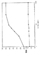
例えばDVB−T規格(2Kモード)であれば、1シンボル内に45個のCP信号が含まれている。このCP信号の角度成分をシンボル間で2回差分をとり(或いは2回差動復調)をし、それらの実数成分(Iチャンネル成分)を1シンボル内で累積加算したとき、その累積加算結果は、理想的には、45となる。すなわち、2回差分をとったとき、CP信号の角度成分は、0に収束するため、その実数成分は、1に収束する。その値を45個累積すれば、45という値になる。
【0144】
ここで、DVB−T規格(2Kモード)のOFDM信号を受信した場合における、1シンボル内すべてのCP信号の二回差動復調した累積加算結果と、CP信号以外の二回差動復調した情報データを45個累積加算した結果とを比較した実験結果を図4に示す。この図4では、横軸に、C/N比をとっている。
【0145】
CP信号の累積加算結果は、C/N比が高い場合には、理想的にはその値が45となるが、ノイズ等が含まれていればその値は減少する。しかしながら、ノイズが大きくなったとしても、ある程度のC/N比が稼げていれば、ある一定の値(例えば20)以下となることはほとんどない。
【0146】
それに対して、CP信号ではない情報データの累積加算結果は、C/N比の大きさに関わらず、その値が、ある一定の値(例えば13)以上となることはほとんどない。
【0147】
従って、閾値を、CP信号の累積加算結果として得られる最小値以下であって、情報データの累積加算結果として得られる最大値以上と設定(具体的に図4に示す例では、13以上20以下)に設定し、広帯域fc誤差・CPE算出回路10によりCP信号として判断された累積加算結果(即ち、シフト量算出回路27から出力されるCP累積加算結果)が、この閾値以下であれば、誤検出をしていると判断することができる。
【0148】
また、TPSやTMCCといった伝送制御情報には、情報データの変調方式や、帯域幅、符号化率等といったデータの復調及び復号のために必要な非常に重要な情報が含まれている。そのため、この伝送制御情報は、通常の情報データよりも誤りに強い変調方式(例えばDBPSK)等を用い、また、複数シンボルに亘り同一情報を伝送し、例えば68シンボルに亘り同一の情報を伝送し、復調の確実性をもたせている。
【0149】
そのため、ノイズによりデータの復調が困難な場合であったとしても、TPSやTMCCといった伝送制御情報は、再生が可能となる。
【0150】
従って、このような伝送情報が復調されていれば、ほぼ正常にキャリア周波数誤差が設定されていると判断することができる。
【0151】
このようにホールド回路14は、CP信号の累積加算結果やTPSやTMCC等の伝送制御情報といった復調の信頼性を示す情報に基づき、広帯域fc誤差・CPE算出回路10が誤検出をしていないかどうかを判断することができる。
【0152】
具体的に、ホールド回路14は、以上のCP信号の累積加算結果や伝送制御情報を用いて、以下のような処理を行う。
【0153】
ホールド回路14は、シフト量演算回路27から広帯域キャリア周波数誤差情報が供給されると、供給された広帯域キャリア周波数誤差情報を、前シンボルにおいて供給された広帯域キャリア周波数誤差情報を比較し、その値が変動したのかどうを判断する。判断を行った結果、前シンボルの広帯域キャリア周波数誤差情報と、当該シンボルの広帯域キャリア周波数誤差情報とが異なった値であった場合、続いて、シフト量算出回路27から供給されたCP累積加算結果が所定の閾値以下であるかどうかを判断する。そして、このCP累積加算結果が所定の閾値以下である場合には、供給された広帯域キャリア周波数誤差情報を更新せずに、前シンボルにおいて供給された広帯域キャリア周波数誤差情報をホールドして、NCO11に供給する。
【0154】
また、例えば、ホールド回路14は、シフト量演算回路27から広帯域キャリア周波数誤差情報が供給されると、供給された広帯域キャリア周波数誤差情報を、前シンボルにおいて供給された広帯域キャリア周波数誤差情報を比較し、その値が変動したのかどうを判断する。判断を行った結果、前シンボルの広帯域キャリア周波数誤差情報と、当該シンボルの広帯域キャリア周波数誤差情報とが異なった値であった場合、続いて、伝送制御信号検出情報が供給されたかどうか(即ち、TPSやTMCC等の伝送制御情報が検出されているかどうか)の判断をする。伝送制御情報が検出されている場合には、供給された広帯域キャリア周波数誤差情報を更新せずに、前シンボルにおいて供給された広帯域キャリア周波数誤差情報をホールドして、NCO11に供給する。
【0155】
以上のようにホールド回路14は、広帯域fc誤差・CPE算出回路10から供給された広帯域キャリア周波数誤差情報の信頼性を判断し、その信頼性が低い場合には広帯域fc誤差・CPE算出回路10が誤検出をしているものとして、広帯域キャリア周波数誤差を前シンボルの値にホールドする。このことにより、ホールド回路14では、雑音やフェージングの影響により正確なキャリア周波数誤差の検出が困難な状態となっても、OFDM信号のキャリア周波数補正制御動作の同期を安定的に保持し、誤動作を防止することができる。
【0156】
なお、このホールド回路14は、広帯域fc誤差・CPE算出回路10から出力される広帯域キャリア周波数誤差情報をホールドするような構成としているが、狭帯域fc誤差算出回路9から出力される情報もホールドするような構成としてもよ。
【0157】
また、ホールド回路14は、CP信号の累積加算値や伝送制御信号に基づき、キャリア周波数の誤検出を行っているか否かを判断しているが、例えば、エラー訂正量等のその他の情報を用いて判断してもよい。
【0158】
【発明の効果】
本発明にかかる復調装置及び復調方法では、キャリア周波数誤差が変動したときに、パイロット信号の角度成分をシンボル間で2回差動復調した実数成分を1シンボル内で累積加算した累積加算値が所定の閾値以下である場合には、キャリア周波数誤差を変動前の値にホールドする。このことにより、本発明では、雑音やフェージングの影響により正確なキャリア周波数誤差の検出が困難な状態となっても、OFDM信号の所定のサブキャリア位置に直交変調されたパイロット信号を用いたキャリア周波数補正制御動作の同期を安定的に保持し、誤動作を防止することができる。
【図面の簡単な説明】
【図1】本発明の実施の形態のOFDM受信装置のブロック構成図である。
【図2】上記OFDM受信装置の要部のブロック構成図である。
【図3】上記OFDM受信装置の広帯域fc誤差・CPE算出回路内のシフト量演算回路のブロック構成図である。
【図4】DVB−T規格のOFDM信号を受信した場合における、1シンボル内すべてのCP信号の二回差動復調した累積加算結果と、CP信号以外の二回差動復調した情報データを45個累積加算した結果とを比較した実験結果を示す図である。
【図5】従来のOFDM受信装置のブロック構成図である。
【図6】OFDM信号のガードインターバルについて説明するための図である。
【図7】OFDM時間領域信号を時間軸方向に平行移動させたときの自己相関関数からOFDMシンボルの境界を求められることを説明するための図である。
【図8】狭帯域キャリア周波数誤差について説明するための図である。
【図9】OFDM周波数領域信号に対して2回のシンボル間の差動復調を行うことよって、CP信号を抽出することができる原理を説明するための図である。
【図10】上記従来のOFDM受信装置の広帯域キャリア周波数誤差算出回路のブロック構成図である。
【図11】上記従来のOFDM受信装置のパイロット信号選択データ発生回路から発生されるCP信号選択データのデータ例を説明する図である。
【図12】上記従来のOFDM受信装置のCPE誤差算出回路のブロック構成図である。
【符号の説明】
1 OFDM受信装置、6 デジタル直交復調回路、7 fc補正回路、8 FFT演算回路、 9 狭帯域fc誤差算出回路、10 広帯域fc誤差算出回路、11 数値制御発振器、12 FFTウィンドウ同期回路、13 CPEキャンセル回路、14 ホールド回路、15 イコライザ、16 検波・エラー訂正回路、17 伝送制御情報復調回路[0001]
BACKGROUND OF THE INVENTION
The present invention relates to a demodulating device and a demodulating method applied to digital broadcasting or the like by an orthogonal frequency division multiplexing (OFDM) system.
[0002]
[Prior art]
In recent years, a modulation method called orthogonal frequency division multiplexing (OFDM) has been proposed as a method for transmitting digital signals. In this OFDM system, a number of orthogonal subcarriers (subcarriers) are provided in a transmission band, data is assigned to the amplitude and phase of each subcarrier, and digitally transmitted by PSK (Phase Shift Keying) or QAM (Quadrature Amplitude Modulation). Modulation method.
[0003]
Since this OFDM scheme divides the transmission band by a large number of subcarriers, the band per subcarrier is narrowed and the modulation speed is slow, but the total transmission speed is the same as the conventional modulation system. have. In addition, this OFDM scheme has a feature that a symbol rate becomes low because a large number of subcarriers are transmitted in parallel. Therefore, this OFDM system can shorten the time length of the multipath relative to the time length of the symbol, and is less susceptible to multipath interference. In the OFDM method, since data is allocated to a plurality of subcarriers, an IFFT (Inverse Frst Fourier Transferorm) arithmetic circuit that performs inverse Fourier transform during modulation, and an FFT (Fast Fourier Transform) that performs Fourier transform during demodulation. ) It has a feature that a transmission / reception circuit can be configured by using an arithmetic circuit.
[0004]
From the above characteristics, the OFDM system is widely studied to be applied to terrestrial digital broadcasting that is strongly affected by multipath interference. Standards such as DVB-T (Digital Video Broadcasting-Terrestrial) and ISDB-T (Integrated Services Digital Broadcasting-Terrestrial) have been proposed as terrestrial digital broadcasting to which such an OFDM system is applied.
[0005]
A digital television broadcast receiver (OFDM receiver) using the OFDM method will be described. FIG. 5 is a block diagram of a conventional OFDM receiver.
[0006]
In FIG. 5, when the signal transmitted between the blocks is a complex signal, the signal component is represented by a thick line, and when the signal transmitted between the blocks is a real signal, the signal component is represented by a thin line. ing.
[0007]
As shown in FIG. 5, the
[0008]
A broadcast wave of a digital television broadcast broadcast from a broadcast station is received by the
[0009]
The RF signal received by the
[0010]
The digital
[0011]
The
[0012]
The
[0013]
Here, the OFDM time domain signal is transmitted in symbol units called OFDM symbols, as shown in FIG. This OFDM symbol is composed of an effective symbol that is a signal period during which IFFT is performed at the time of transmission, and a guard interval in which a waveform of a part of the latter half of the effective symbol is copied as it is. This guard interval is provided in the first half of the OFDM symbol. In the OFDM method, such a guard interval is provided to improve multipath tolerance. For example, in the DVB-T standard (2K mode), 2048 subcarriers are included in an effective symbol, and the subcarrier interval is 4.464 kHz. In addition, data is modulated to 1705 subcarriers out of 2048 subcarriers in the effective symbol. Further, the guard interval is a signal having a time length of 1/4 of the effective symbol. Note that, in the DVB-T standard (2K mode), the
[0014]
The
[0015]
As described above, the OFDM frequency domain signal output from the
[0016]
The narrowband fc error calculation circuit 108 and the wideband fc
[0017]
The
[0018]
The FFT
[0019]
The
[0020]
The
[0021]
The detection /
[0022]
The transmission control
[0023]
Next, the operating principle of the narrowband fc error calculation circuit 108 will be described.
[0024]
The narrowband fc error calculation circuit 108 obtains a correlation between the waveform of the guard interval portion and the waveform of the latter half portion of the OFDM symbol (that is, the signal waveform of the copy source of the guard interval) for the OFDM time domain signal. A boundary portion of the OFDM symbol is obtained based on the correlation.
[0025]
Specifically, as shown in FIG. 7A, when the guard interval period is Tg (time) and the effective symbol period is Tu (time), an OFDM time domain signal (f ( The autocorrelation function (integral region is Tg) when t)) is translated by Tu in the time axis direction is obtained, and the peak position of the autocorrelation function is set as the boundary of the OFDM symbol.
[0026]
[Expression 1]
That is, an OFDM time domain signal (f (t + Tu)) translated from Tu time as shown in FIG. 7B with respect to the original OFDM time domain signal (f (t)) as shown in FIG. ), (F (t)) and (f (t + Tu)) are multiplied, and the function obtained by the multiplication is integrated over time. A function obtained by this time integration is an autocorrelation function (Corr (t)). The highest peak portion of the autocorrelation function (Corr (t)) is a portion highly correlated with the guard interval. Therefore, the time indicated by the highest peak value of the autocorrelation function (Corr (t)) as shown in FIG. 7C indicates the time that coincides with the waveform that is the copy source of the guard interval. Therefore, that time becomes the boundary of the OFDM symbol.
[0028]
Here, the autocorrelation function (Corr (t)) thus obtained is a complex signal as shown in the above equation, and its phase component is proportional to the carrier frequency error. Therefore, the narrowband fc error calculation circuit 108 obtains an autocorrelation value at the boundary portion of such an OFDM symbol and outputs the phase in the autocorrelation value as a carrier frequency error. However, since the carrier frequency error obtained from the autocorrelation function is repeated in a sawtooth manner at the subcarrier frequency interval as shown in FIG. 8, the detection range is ± 1/2 or less of the subcarrier frequency interval. It becomes accuracy information. Thus, the information on the narrow band carrier frequency error obtained by the narrow band fc error calculation circuit 108 is supplied to the
[0029]
Further, the peak position information calculated by the narrowband fc error calculation circuit 108 indicates the boundary of the OFDM symbol as described above. The OFDM symbol boundary information obtained by the narrowband fc error calculation circuit 108 is supplied to the FFT
[0030]
Next, the broadband fc
[0031]
First, the calculation principle of the carrier frequency error by the broadband fc
[0032]
The OFDM signal generally includes a pilot signal called a CP (Continual Pilots) signal. This CP signal is a signal that always represents a specific phase and amplitude, and is inserted into subcarriers of a plurality of indexes within an effective symbol. The number of CP signals included in the effective symbol and the arrangement pattern of the insertion positions are determined in advance by the standard. For example, in the DVB-T standard (2K mode), there are 2048 subcarriers (0 to 2047) in one effective symbol, among which 45 subcarriers contain CP signals. Also, in this DVB-T standard (2K mode), the CP signal arrangement pattern is 0, 48, 54, 87, 141 with subcarrier index numbers (within the range of 1705 signals are modulated). 156, 192, 201, 255, 279, 282, 333, 432, 450, 483, 525, 531, 618, 636, 714, 759, 765, 780, 804, 873, 888, 918, 939, 942, 969 984, 1050, 1101, 1107, 1110, 1137, 1140, 1146, 1206, 1269, 1323, 1377, 1491, 1683, 1704.
[0033]
The wideband fc
[0034]
The principle that a CP signal can be extracted by performing differential demodulation between two symbols on an OFDM frequency domain signal will be described with reference to FIG.
[0035]
FIG. 9 is a diagram for explaining phase transition between normal information data and a CP signal for explaining differential demodulation between symbols at the first stage and differential demodulation between symbols at the second stage. In FIG. 9, it is assumed that the information data is QPSK (Quadrature Phase Shift Keying) modulated, and the CP signal is modulated with information on signal points of a specific amplitude and phase. .
[0036]
FIG. 9A shows the I channel signal and the Q channel signal decomposed for each frequency component of each subcarrier by the FFT for each symbol (n−1th symbol, nth symbol, n + 1th symbol). It is shown on the phase plane. an and bn indicate information data whose subcarrier index numbers after FFT of the nth OFDM symbol are a and b, respectively, and can and cbn are subcarriers after FFT of the nth OFDM symbol. CP signals having carrier index numbers ca and cb are shown. The CP signal originally has constant amplitude and phase information, but there may be some phase rotation for each symbol due to the influence of a reproduced carrier frequency error or the like.
[0037]
FIG. 9B shows, on the phase plane, one-time differential demodulated data when the information of the same index number is subjected to one-time differential demodulation between symbols. dan and dbn are the once-differential demodulated data of the (n-1) th symbol and the nth symbol whose subcarrier index numbers are a and b, respectively. Further, dcan and dcbn are the once-differential demodulated data of the (n-1) th symbol and the nth symbol whose subcarrier index numbers are ca and cb, respectively.
[0038]
FIG. 9C shows twice differential demodulated data on the phase plane when the information of the same index number is subjected to differential demodulation twice between symbols. dda and ddb are obtained by differentially demodulating the (n-1) th symbol and the nth symbol with index numbers a and b of the subcarrier, respectively, the nth symbol and the (n + 1) th symbol. The differential demodulated data obtained as a result of differential demodulation of the symbol obtained by differential demodulating the symbol of Ddca and ddcb are obtained by differentially demodulating the (n−1) th symbol and the nth symbol of the subcarrier index numbers ca and cb, the nth symbol and the (n + 1) th symbol, respectively. This is twice-differential demodulated data obtained as a result of further differential demodulation of the symbol demodulated from the second symbol.
[0039]
Since the CP signals ca and cb are signals having a constant phase, the FFT window phase error and the carrier phase error are excluded in the first differential demodulation and depend on the carrier frequency error, the CPE, and the reproduction clock frequency error. A phase error will remain. Since any phase error remaining after the first differential demodulation does not depend on time, it is constant between the data after differential demodulation. Therefore, by performing the second differential demodulation between the data subjected to the first differential demodulation, the phase error depending on the CPE and the reproduction clock frequency remaining in the first differential demodulation is removed. Can do. As a result, the CP signal converges to a positive value on the I axis (see FIG. 9C).
[0040]
On the other hand, since the information data a and b take a random phase between symbols, the phase becomes random for each data even after the differential demodulation is performed twice. Disperse randomly on top.
[0041]
Therefore, for example, if only the I-axis data of the CP signal is accumulated and added within one symbol, this CP signal converges to a certain value on the I-axis, so the I-axis data from which only the information data is extracted is accumulated. The value is much larger than the result of addition. Therefore, the subcarrier position of the CP signal can be estimated from the maximum value of this cumulative addition. Then, by calculating how much the estimated subcarrier position of the CP signal is shifted from the original subcarrier arrangement position, the carrier frequency error can be calculated with subcarrier interval accuracy.
[0042]
Next, a specific circuit example of the wideband fc
[0043]
FIG. 10 shows a block configuration diagram of the broadband fc
[0044]
The wideband fc
[0045]
The first
[0046]
The first
(I + jQ) (I-1-JQ-1)
Then, the first
[0047]
The second differential demodulator circuit 122 has the same configuration as the first
[0048]
The
[0049]
The pilot signal selection
[0050]
A data example of the CP signal selection data generated from the pilot signal selection
[0051]
When the shift amount fe = Δf is supplied, the pilot signal selection
[0052]
On the other hand, when a negative shift amount fe = −Δf is supplied, the pilot signal selection
[0053]
The CP signal selection data supplied to the
[0054]
The
[0055]
The maximum
[0056]
The carrier frequency error storage circuit 128 includes a selector 138 and a
[0057]
The gate circuit 129 latches the shift amount fe stored in the
[0058]
By performing the processing as described above, the wideband fc
[0059]
Next, the
[0060]
The CPE cancel
[0061]
The
[0062]
The
[0063]
The averaging
[0064]
Tan-1The
[0065]
The
[0066]
The
[0067]
On the other hand, the OFDM frequency domain signal output from the
[0068]
The
[0069]
[Problems to be solved by the invention]
As described above, the conventional OFDM receiving apparatus extracts a CP signal from the frequency domain signal after the FFT operation, and detects a carrier frequency error in a wide band of the OFDM signal from the shift amount of the CP signal. Specifically, using the fact that the phase component of the CP signal is 0, differential demodulation between two symbols is performed on complex data after FFT demodulation, and differential demodulation between two symbols is performed. A signal whose detection result is 0 was extracted as a CP signal.
[0070]
However, when the CP signal is attenuated due to deterioration of the transmission path or reception state, noise energy becomes larger than the energy of the CP signal, and a signal other than the CP signal may be erroneously detected as a CP signal. There is. Thus, if a signal other than the CP signal is erroneously detected as a CP signal, the carrier frequency error fluctuates and the carrier frequency correction is out of synchronization.
[0071]
An object of the present invention is to provide a demodulation device and a demodulation method capable of solving the above-described problems and stably maintaining the synchronization of the carrier frequency correction control operation of the OFDM signal.
[0072]
[Means for Solving the Problems]
A demodulator according to the present invention is a demodulator that demodulates an orthogonal frequency division multiplexing (OFDM) signal,A pilot signal with the same phase component was quadrature modulated at a predetermined subcarrier position in the symbol.With OFDM signalCarrier frequency error correction signal andThe carrier frequency correction means for correcting the carrier frequency of the OFDM signal by complex multiplication, and the OFDM signal whose carrier frequency has been corrected by the carrier frequency correction means by Fourier transform in units of one symbol period to each subcarrier Fourier transform means for demodulating the information modulated to generate a frequency domain signal, and the frequency domain signal demodulated by the Fourier transform meansAnd detecting the pilot signal from the pilot signalBased on the above, the carrier frequency error of the OFDM signal is calculatedIn addition, a cumulative addition value is calculated by accumulating the real number component obtained by differentially demodulating the angle component of the pilot signal twice between symbols within one symbol.Carrier frequency error calculation means, frequency error correction signal generation means for generating the frequency error correction signal based on the carrier frequency error of the OFDM signal calculated by the carrier frequency error calculation means, and carrier frequency error calculation means When the calculated carrier frequency error fluctuates,If the cumulative added value is below a predetermined threshold,Holding means for holding the carrier frequency error output from the carrier frequency error calculating means at a value before fluctuation;The
[0074]
A demodulation method according to the present invention is a demodulation method for demodulating an orthogonal frequency division multiplexing (OFDM) signal,A pilot signal with the same phase component was quadrature modulated at a predetermined subcarrier position in the symbol.The frequency domain signal is generated by demodulating the information modulated on each subcarrier by Fourier transforming the OFDM signal in units of one symbol period, and generating the frequency domain signal.And detecting the pilot signal from the pilot signalCalculate the carrier frequency error of the OFDM signal based onIn addition, the cumulative addition value is calculated by accumulating the real number component obtained by differentially demodulating the angle component of the pilot signal twice between symbols within one symbol.And based on the calculated carrier frequency error of the OFDM signal, ZhouWhen a wave number error correction signal is generated, the carrier frequency error correction signal and the OFDM signal are complex-multiplied to correct the carrier frequency of the OFDM signal, and the calculated carrier frequency error fluctuates.If the cumulative added value is below a predetermined threshold,Hold the carrier frequency error to the value before the fluctuation.The
[0076]
DETAILED DESCRIPTION OF THE INVENTION
In the following, as an embodiment of the present invention, a digital broadcast receiving apparatus (OFDM receiving apparatus) using the OFDM system to which the present invention is applied will be described.
[0077]
FIG. 1 is a block diagram of an OFDM receiving apparatus to which the present invention is applied. In FIG. 1, when the signal transmitted between the blocks is a complex signal, the signal component is represented by a thick line, and when the signal transmitted between the blocks is a real signal, the signal component is represented by a thin line. Yes.
[0078]
As shown in FIG. 1, the
[0079]
A broadcast wave of digital television broadcast broadcast from a broadcast station is received by the
[0080]
The RF signal received by the
[0081]
The digital orthogonal demodulation circuit 6 orthogonally demodulates the digitized IF signal using a carrier signal having a predetermined frequency (fc: carrier frequency), and outputs a baseband OFDM signal. Since the baseband OFDM signal output from the digital quadrature demodulation circuit 6 is a so-called time domain signal before FFT (Fast Fourier Transferorm) calculation, it is hereinafter referred to as an OFDM time domain signal. As a result of orthogonal demodulation, the OFDM time domain signal is a complex signal including a real axis component (I channel signal) and an imaginary axis component (Q channel signal). The OFDM time domain signal output from the digital quadrature demodulation circuit 6 is supplied to the fc correction circuit 7.
[0082]
The fc correction circuit 7 performs complex multiplication of the carrier frequency error correction signal output from the
[0083]
The FFT operation circuit 8 performs an FFT operation on the OFDM time domain signal, and extracts and outputs data modulated for each subcarrier. Since the signal output from the FFT operation circuit 8 is a so-called frequency domain signal after being subjected to FFT, it is hereinafter referred to as an OFDM frequency domain signal.
[0084]
The FFT operation circuit 8 performs an FFT operation on an effective symbol length range (a 2048 sample range) obtained by removing a signal corresponding to the guard interval time length from the OFDM symbol. The calculation range (FFT window) is controlled by the FFT window synchronization circuit 12. Specifically, the calculation start position is any position between the boundary of the OFDM symbol and the end position of the guard interval.
[0085]
As described above, the OFDM frequency domain signal output from the FFT operation circuit 8 is a complex signal composed of a real axis component (I channel signal) and an imaginary axis component (Q channel signal), like the OFDM time domain signal. ing. The OFDM frequency domain signal is supplied to the broadband fc error /
[0086]
The narrowband fc
[0087]
The wideband fc error /
[0088]
The
[0089]
The FFT window synchronization circuit 12 is based on OFDM symbol boundary position information obtained when the narrowband fc
[0090]
The CPE cancel
[0091]
The
[0092]
The detection / error correction circuit 16 detects information modulated on each subcarrier according to the modulation method, and performs demapping and decodes the data. Thereafter, the detection / error correction circuit 16 performs error correction processing on the decoded data and outputs, for example, an MPEG-2 transport stream.
[0093]
The transmission control
[0094]
Next, the broadband fc error /
[0095]
First, the calculation principle of the broadband carrier frequency error by the broadband fc error /
[0096]
The OFDM signal includes a pilot signal called a CP (Continual Pilots) signal. This CP signal is a signal that always represents a specific phase and amplitude, and is inserted into subcarriers of a plurality of indexes within an effective symbol. The number of CP signals included in the effective symbol and the arrangement pattern of the insertion positions are determined in advance by the standard. For example, in the DVB-T standard (2K mode), there are 2048 subcarriers (0 to 2047) in one effective symbol, among which 45 subcarriers contain CP signals. The specific subcarrier index number into which the CP signal is inserted is as described in the conventional example.
[0097]
The wideband fc error /
[0098]
Further, the wideband fc error /
[0099]
A specific circuit example of the wideband fc error /
[0100]
FIG. 2 is a block diagram of the wideband fc error /
[0101]
The broadband fc error /
[0102]
The
[0103]
The first 1-
[0104]
The
[0105]
The
[0106]
Similarly to the first one
[0107]
Similarly to the
[0108]
The
[0109]
The
[0110]
The shift
[0111]
Specifically, a circuit example of the shift
[0112]
As shown in FIG. 3, the shift
[0113]
The memory 41 stores twice-difference data (I channel signal) between symbols for one symbol output from the
[0114]
The pilot signal selection
[0115]
The CP signal selection data generated from the pilot signal selection
[0116]
The CP signal selection data to be supplied to the memory 41 as a read address is, for example, 21 patterns of CP signal selection as shown in FIG. 11 until the twice-difference data stored in the memory 41 is updated. Data is generated sequentially. That is, during one symbol period, a shift amount of −10Δf to 10Δf is sequentially supplied to the pilot signal selection
[0117]
The
[0118]
The maximum
[0119]
Specifically, the
[0120]
The maximum value of the cumulative addition result (CP value cumulative addition result) stored in the
[0121]
The carrier frequency
[0122]
Then, the
[0123]
As described above, the wideband fc error /
[0124]
Further, the wideband fc error /
[0125]
The
[0126]
The averaging
[0127]
The cumulative addition circuit 33 cumulatively adds the supplied phase fluctuation amount (angle data) for each symbol. By accumulating the phase fluctuation component for each symbol, it becomes possible to follow the phase fluctuation of the OFDM signal. The cumulatively added angle data is supplied to the
[0128]
The
[0129]
On the other hand, the OFDM frequency domain signal output from the FFT operation circuit 8 is delayed by one symbol by the one
[0130]
The
[0131]
As described above, the wideband fc error /
[0132]
The broadband fc error /
[0133]
In the above broadband fc error /
[0134]
When the data modulated on each subcarrier is modulated by a method such as BPSK or QPSK, the 1-
[0135]
Next, the
[0136]
The
[0137]
While performing such processing, the
[0138]
In general, if the demodulation state of the OFDM signal is in a stable operation state, the carrier frequency error hardly fluctuates, so that the wideband carrier frequency error hardly fluctuates. Therefore, the value of the output from the shift
[0139]
Here, when the carrier frequency does not change but the true carrier frequency cannot be detected due to the influence of noise or the like, that is, when the carrier frequency is erroneously detected, the carrier frequency is based on the erroneous detection information. If the error is corrected, the reception state deteriorates and the carrier frequency cannot be locked.
[0140]
Therefore, in the
[0141]
Specifically, as information for judging reliability of the fluctuation, judgment is made by using a cumulative addition result within one symbol of a CP signal obtained by taking a difference twice, a reproduction result of transmission control information such as TPS and TMCC, and the like. It is possible.
[0142]
Here, the reason why the cumulative addition result within one symbol of the CP signal and the transmission control information such as TPS and TMCC can be used as the information for determining the reliability is as follows.
[0143]
For example, in the DVB-T standard (2K mode), 45 CP signals are included in one symbol. When the angular component of this CP signal is differentiated twice between symbols (or twice differentially demodulated) and those real components (I channel components) are cumulatively added within one symbol, the cumulative addition result is Ideally, 45. That is, when the difference is taken twice, the angle component of the CP signal converges to 0, so that the real component converges to 1. If 45 values are accumulated, the value becomes 45.
[0144]
Here, when an OFDM signal of the DVB-T standard (2K mode) is received, a cumulative addition result obtained by performing differential demodulation twice of all CP signals in one symbol and information obtained by performing differential demodulation other than the CP signal twice. FIG. 4 shows the result of an experiment comparing the result of cumulative addition of 45 data. In FIG. 4, the horizontal axis represents the C / N ratio.
[0145]
The cumulative addition result of the CP signal ideally has a value of 45 when the C / N ratio is high, but the value decreases if noise or the like is included. However, even if the noise increases, it is rarely below a certain value (for example, 20) as long as a certain C / N ratio can be obtained.
[0146]
On the other hand, the cumulative addition result of information data that is not a CP signal hardly has a certain value (for example, 13) or more regardless of the size of the C / N ratio.
[0147]
Therefore, the threshold value is set to be equal to or less than the minimum value obtained as the cumulative addition result of the CP signal and equal to or more than the maximum value obtained as the cumulative addition result of the information data (specifically, in the example shown in FIG. 4, from 13 to 20). ) And the cumulative addition result determined as the CP signal by the broadband fc error / CPE calculation circuit 10 (that is, the CP cumulative addition result output from the shift amount calculation circuit 27) is less than or equal to this threshold value, an error occurs. It can be determined that detection is being performed.
[0148]
The transmission control information such as TPS and TMCC includes very important information necessary for data demodulation and decoding, such as information data modulation scheme, bandwidth, coding rate, and the like. Therefore, this transmission control information uses a modulation scheme (for example, DBPSK) that is more resistant to errors than normal information data, transmits the same information over a plurality of symbols, and transmits the same information over 68 symbols, for example. It has certainty of demodulation.
[0149]
For this reason, even if it is difficult to demodulate data due to noise, transmission control information such as TPS and TMCC can be reproduced.
[0150]
Therefore, if such transmission information is demodulated, it can be determined that the carrier frequency error is set almost normally.
[0151]
In this way, the
[0152]
Specifically, the
[0153]
When the wideband carrier frequency error information is supplied from the shift
[0154]
Further, for example, when the wide band carrier frequency error information is supplied from the shift
[0155]
As described above, the
[0156]
The
[0157]
The
[0158]
【The invention's effect】
In the demodulation device and the demodulation method according to the present invention, when the carrier frequency error fluctuates,When the accumulated addition value obtained by accumulating the real number component obtained by differentially demodulating the angle component of the pilot signal twice between symbols within one symbol is equal to or less than a predetermined threshold value,Hold the carrier frequency error to the value before the change. As a result, in the present invention, even if it is difficult to detect an accurate carrier frequency error due to the influence of noise and fading,Using a pilot signal quadrature modulated at a predetermined subcarrier positionIt is possible to stably maintain the synchronization of the carrier frequency correction control operation and prevent malfunction.
[Brief description of the drawings]
FIG. 1 is a block configuration diagram of an OFDM receiver according to an embodiment of the present invention.
FIG. 2 is a block diagram of a main part of the OFDM receiver.
FIG. 3 is a block configuration diagram of a shift amount calculation circuit in a wideband fc error / CPE calculation circuit of the OFDM receiver.
FIG. 4 shows 45 cumulative addition results obtained by differentially demodulating all CP signals in one symbol twice, and information data obtained by differentially demodulating twice other than CP signals when receiving an DVB-T standard OFDM signal. It is a figure which shows the experimental result compared with the result which carried out cumulative addition.
FIG. 5 is a block diagram of a conventional OFDM receiver.
FIG. 6 is a diagram for explaining a guard interval of an OFDM signal.
FIG. 7 is a diagram for explaining that an OFDM symbol boundary can be obtained from an autocorrelation function when an OFDM time domain signal is translated in the time axis direction;
FIG. 8 is a diagram for explaining a narrow-band carrier frequency error.
FIG. 9 is a diagram for explaining the principle that a CP signal can be extracted by performing differential demodulation between symbols twice for an OFDM frequency domain signal.
FIG. 10 is a block configuration diagram of a broadband carrier frequency error calculation circuit of the conventional OFDM receiver.
FIG. 11 is a diagram illustrating a data example of CP signal selection data generated from a pilot signal selection data generation circuit of the conventional OFDM receiver.
FIG. 12 is a block configuration diagram of a CPE error calculation circuit of the conventional OFDM receiver.
[Explanation of symbols]
DESCRIPTION OF
Claims (4)
位相成分が同一とされたパイロット信号がシンボル内の所定のサブキャリア位置に直交変調されたOFDM信号とキャリア周波数誤差補正信号とを複素乗算して、上記OFDM信号のキャリア周波数を補正するキャリア周波数補正手段と、
上記キャリア周波数補正手段によりキャリア周波数が補正された上記OFDM信号を、1シンボル期間単位でフーリエ変換して各サブキャリアに変調されている情報を復調し、周波数領域信号を生成するフーリエ変換手段と、
上記フーリエ変換手段により復調された上記周波数領域信号から上記パイロット信号を検出し、上記パイロット信号に基づき、上記OFDM信号のキャリア周波数誤差を算出するとともに、上記パイロット信号の角度成分をシンボル間で2回差動復調した実数成分を1シンボル内で累積加算した累積加算値を算出するキャリア周波数誤差算出手段と、
上記キャリア周波数誤差算出手段により算出された上記OFDM信号のキャリア周波数誤差に基づき、上記周波数誤差補正信号を生成する周波数誤差補正信号生成手段と、
上記キャリア周波数誤差算出手段により算出されたキャリア周波数誤差が変動したときに、上記累積加算値が所定の閾値以下である場合には、上記キャリア周波数誤差算出手段から出力されるキャリア周波数誤差を変動前の値にホールドするホールド手段とを備える復調装置。In a demodulator for demodulating an Orthogonal Frequency Division Multiplex (OFDM) signal,
Carrier frequency correction that corrects the carrier frequency of the OFDM signal by performing complex multiplication of the OFDM signal obtained by orthogonally modulating the pilot signal having the same phase component at a predetermined subcarrier position in the symbol and the carrier frequency error correction signal. Means,
Fourier transform means for generating a frequency domain signal by demodulating information modulated on each subcarrier by Fourier transforming the OFDM signal whose carrier frequency has been corrected by the carrier frequency correction means in units of one symbol period;
The pilot signal is detected from the frequency domain signal demodulated by the Fourier transform means, the carrier frequency error of the OFDM signal is calculated based on the pilot signal, and the angle component of the pilot signal is calculated twice between symbols. A carrier frequency error calculating means for calculating a cumulative addition value obtained by cumulatively adding the real component subjected to differential demodulation within one symbol ;
Frequency error correction signal generation means for generating the frequency error correction signal based on the carrier frequency error of the OFDM signal calculated by the carrier frequency error calculation means;
When the carrier frequency error calculated by the carrier frequency error calculation means fluctuates, if the cumulative added value is less than or equal to a predetermined threshold, the carrier frequency error output from the carrier frequency error calculation means is changed to A demodulator comprising hold means for holding the value of.
上記ホールド手段は、上記キャリア周波数誤差算出手段により算出されたキャリア周波数誤差が変動したときに、上記伝送制御信号が正常に復号されている場合には、上記キャリア周波数誤差算出手段から出力されるキャリア周波数誤差を変動前の値にホールドする請求項1記載の復調装置。In the OFDM signal, a transmission control signal is orthogonally modulated to subcarriers,
When the carrier frequency error calculated by the carrier frequency error calculating means fluctuates and the transmission control signal is normally decoded, the holding means outputs a carrier output from the carrier frequency error calculating means. demodulator of 請 Motomeko 1, wherein you hold the frequency error value before change.
位相成分が同一とされたパイロット信号がシンボル内の所定のサブキャリア位置に直交変調されたOFDM信号を1シンボル期間単位でフーリエ変換することによって各サブキャリアに変調されている情報を復調して周波数領域信号を生成し、
上記周波数領域信号から上記パイロット信号を検出し、上記パイロット信号に基づき、上記OFDM信号のキャリア周波数誤差を算出するとともに、上記パイロット信号の角度成分をシンボル間で2回差動復調した実数成分を1シンボル内で累積加算した累積加算値を算出し、
算出された上記OFDM信号のキャリア周波数誤差に基づき、周波数誤差補正信号を生成し、
上記キャリア周波数誤差補正信号と上記OFDM信号とを複素乗算して、上記OFDM信号のキャリア周波数を補正し、
算出された上記キャリア周波数誤差が変動したときに、上記累積加算値が所定の閾値以下である場合には、上記キャリア周波数誤差を変動前の値にホールドする復調方法。In a demodulation method for demodulating an orthogonal frequency division multiplexing (OFDM) signal,
An OFDM signal obtained by orthogonally modulating a pilot signal having the same phase component to a predetermined subcarrier position in a symbol is Fourier-transformed in units of one symbol period to demodulate information modulated on each subcarrier. Generate a region signal,
The pilot signal is detected from the frequency domain signal, the carrier frequency error of the OFDM signal is calculated based on the pilot signal, and the real component obtained by differentially demodulating the angle component of the pilot signal twice between symbols is 1 Calculate the cumulative addition value that is cumulatively added within the symbol ,
Based on the carrier frequency error of the calculated the OFDM signal to generate a frequency error correction signal,
Complex multiplication of the carrier frequency error correction signal and the OFDM signal to correct the carrier frequency of the OFDM signal,
When calculated the carrier frequency error is changed, if the cumulative addition value is equal to or less than the predetermined threshold value, demodulation how to hold the value before change of the carrier frequency error.
算出されたキャリア周波数誤差が変動したときに、上記伝送制御信号が正常に復号されている場合には、上記キャリア周波数誤差を変動前の値にホールドする請求項3記載の復調方法。The OFDM signal is obtained by orthogonally modulating a transmission control signal to subcarriers,
When the calculated carrier frequency error is changed, if the transmission control signal is decoded successfully, 請 Motomeko 3 demodulating method according you hold the value before change of the carrier frequency error.
Priority Applications (4)
| Application Number | Priority Date | Filing Date | Title |
|---|---|---|---|
| JP2000210331A JP4356203B2 (en) | 2000-07-11 | 2000-07-11 | Demodulator and demodulation method |
| DE60128036T DE60128036T2 (en) | 2000-07-11 | 2001-07-09 | Vehicle recovery in a multi-carrier receiver |
| EP01305884A EP1172982B1 (en) | 2000-07-11 | 2001-07-09 | Carrier recovery in a multicarrier receiver |
| US09/901,731 US6720824B2 (en) | 2000-07-11 | 2001-07-10 | Demodulation method and apparatus |
Applications Claiming Priority (1)
| Application Number | Priority Date | Filing Date | Title |
|---|---|---|---|
| JP2000210331A JP4356203B2 (en) | 2000-07-11 | 2000-07-11 | Demodulator and demodulation method |
Publications (2)
| Publication Number | Publication Date |
|---|---|
| JP2002026866A JP2002026866A (en) | 2002-01-25 |
| JP4356203B2 true JP4356203B2 (en) | 2009-11-04 |
Family
ID=18706614
Family Applications (1)
| Application Number | Title | Priority Date | Filing Date |
|---|---|---|---|
| JP2000210331A Expired - Lifetime JP4356203B2 (en) | 2000-07-11 | 2000-07-11 | Demodulator and demodulation method |
Country Status (4)
| Country | Link |
|---|---|
| US (1) | US6720824B2 (en) |
| EP (1) | EP1172982B1 (en) |
| JP (1) | JP4356203B2 (en) |
| DE (1) | DE60128036T2 (en) |
Families Citing this family (34)
| Publication number | Priority date | Publication date | Assignee | Title |
|---|---|---|---|---|
| WO2003001760A1 (en) * | 2001-06-22 | 2003-01-03 | Thomson Licensing S.A. | Method and system for compensation of a carrier frequency offset in an ofdm receiver |
| JP2003069526A (en) * | 2001-08-22 | 2003-03-07 | Clarion Co Ltd | Ofdm demodulation device and its carrier frequency synchronous method |
| JPWO2003032543A1 (en) * | 2001-09-28 | 2005-01-27 | 富士通株式会社 | Automatic frequency control apparatus and method for OFDM |
| JP3538187B2 (en) | 2002-03-26 | 2004-06-14 | 株式会社東芝 | OFDM receiver and data demodulation method in OFDM receiver |
| US7346131B2 (en) * | 2002-07-10 | 2008-03-18 | Zoran Corporation | System and method for pre-FFT OFDM fine synchronization |
| JP2004214961A (en) * | 2002-12-27 | 2004-07-29 | Sony Corp | Ofdm demodulator |
| JP4109556B2 (en) * | 2003-01-31 | 2008-07-02 | 松下電器産業株式会社 | OFDM signal collision position detection apparatus, OFDM reception apparatus, OFDM signal collision position detection method, and OFDM reception method |
| JP4461095B2 (en) * | 2003-03-10 | 2010-05-12 | パナソニック株式会社 | OFDM signal transmission method, transmitter, and receiver |
| ATE375667T1 (en) * | 2003-06-30 | 2007-10-15 | Nokia Corp | FASTER FINE TIMING OPERATION IN A MULTI CARRIER SYSTEM |
| KR100510551B1 (en) * | 2003-10-10 | 2005-08-26 | 삼성전자주식회사 | OFDM demodulator with common phase error(CPE) correction and CPE removing method |
| US8311152B1 (en) | 2004-02-27 | 2012-11-13 | Marvell International Ltd. | Adaptive OFDM receiver based on carrier frequency offset |
| DE102004021860B4 (en) * | 2004-05-04 | 2010-04-29 | Infineon Technologies Ag | Phase and frequency tracking of an OFDM receiver using pilot-assisted phase estimation |
| TWI245199B (en) * | 2004-08-10 | 2005-12-11 | Ali Corp | Blind channel searching and estimation method using fast Fourier transformation |
| GB2422257B (en) * | 2004-10-18 | 2008-10-01 | Zarlink Semiconductor Ltd | Tuner |
| US7765086B2 (en) * | 2004-12-09 | 2010-07-27 | Tektronix, Inc. | Modulation domain trigger |
| JPWO2006098050A1 (en) * | 2005-03-16 | 2008-08-21 | 富士通株式会社 | Diversity receiver |
| WO2007013226A1 (en) * | 2005-07-29 | 2007-02-01 | Matsushita Electric Industrial Co., Ltd. | Receiver apparatus and electronic device using the same |
| US7983350B1 (en) * | 2005-10-25 | 2011-07-19 | Altera Corporation | Downlink subchannelization module |
| EP2037605A4 (en) * | 2006-06-30 | 2014-07-16 | Fujitsu Ltd | Digital mobile communication system and its transmission/reception method |
| DE102007017838A1 (en) * | 2007-01-10 | 2008-07-17 | Rohde & Schwarz Gmbh & Co. Kg | Device and method for determining and displaying a synchronization state |
| KR101406160B1 (en) | 2007-06-29 | 2014-06-12 | 톰슨 라이센싱 | Apparatus and method for removing common phase error in a dvb-t/h receiver |
| EP2171896A4 (en) * | 2007-06-29 | 2012-06-06 | Thomson Licensing | Apparatus and method for removing common phase error in a dvb-t/h receiver |
| JP4359638B2 (en) * | 2007-08-24 | 2009-11-04 | Okiセミコンダクタ株式会社 | Correlation calculator and correlation calculator |
| US20090059782A1 (en) * | 2007-08-29 | 2009-03-05 | Rgb Systems, Inc. | Method and apparatus for extending the transmission capability of twisted pair communication systems |
| EP2081343A2 (en) * | 2008-01-17 | 2009-07-22 | Core Logic, Inc. | Estimating frequency shift |
| JP5752870B2 (en) * | 2008-03-14 | 2015-07-22 | 独立行政法人石油天然ガス・金属鉱物資源機構 | Operation method of hydrotreating equipment |
| JP2010068194A (en) * | 2008-09-10 | 2010-03-25 | Mitsubishi Electric Corp | Carrier frequency error detection device |
| JP5225812B2 (en) * | 2008-11-17 | 2013-07-03 | シャープ株式会社 | OFDM demodulation apparatus, OFDM demodulation method, program, and computer-readable recording medium |
| DE102009017552B3 (en) * | 2009-04-17 | 2010-09-30 | Sew-Eurodrive Gmbh & Co. Kg | Apparatus and method for contactless transmission of electrical power and information |
| CN102144365B (en) | 2009-07-02 | 2014-12-10 | 松下电器产业株式会社 | Receiver device, and receiving method |
| TWI551064B (en) * | 2012-12-27 | 2016-09-21 | 晨星半導體股份有限公司 | Wireless receiver and method for estimating channel effect thereof |
| JP6164965B2 (en) * | 2013-07-26 | 2017-07-19 | 京セラ株式会社 | Receiving apparatus and receiving method |
| US10218548B1 (en) * | 2018-01-24 | 2019-02-26 | National Instruments Corporation | Wireless radio receiver that performs adaptive phase tracking |
| US10218549B1 (en) | 2018-01-24 | 2019-02-26 | National Instruments Corporation | Wireless radio receiver that performs adaptive phase tracking |
Family Cites Families (9)
| Publication number | Priority date | Publication date | Assignee | Title |
|---|---|---|---|---|
| FR2670062B1 (en) * | 1990-11-30 | 1993-11-12 | Thomson Csf | METHOD FOR RECALARING THE LOCAL OSCILLATORS OF A RECEIVER AND DEVICE FOR CARRYING OUT THE METHOD. |
| EP0772332A3 (en) * | 1995-11-02 | 2000-10-11 | British Broadcasting Corporation | Synchronisation of OFDM signals |
| US5825241A (en) * | 1995-12-11 | 1998-10-20 | Delco Electronics Corporation | Differential demodulator |
| JP3556047B2 (en) * | 1996-05-22 | 2004-08-18 | 三菱電機株式会社 | Digital broadcast receiver |
| ATE384401T1 (en) * | 1997-05-02 | 2008-02-15 | Lsi Logic Corp | DEMODULATION OF DIGITAL VIDEO BROADCAST SIGNALS |
| JP2907804B1 (en) * | 1998-01-30 | 1999-06-21 | 株式会社次世代デジタルテレビジョン放送システム研究所 | OFDM receiver |
| KR100252971B1 (en) * | 1998-02-25 | 2000-04-15 | 구자홍 | Automatic frequency control method of digital broadcasting receiver |
| JP3519291B2 (en) * | 1998-11-06 | 2004-04-12 | 松下電器産業株式会社 | OFDM communication apparatus and method |
| US6594320B1 (en) * | 1999-08-25 | 2003-07-15 | Lucent Technologies, Inc. | Orthogonal Frequency Division Multiplexed (OFDM) carrier acquisition method |
-
2000
- 2000-07-11 JP JP2000210331A patent/JP4356203B2/en not_active Expired - Lifetime
-
2001
- 2001-07-09 EP EP01305884A patent/EP1172982B1/en not_active Expired - Lifetime
- 2001-07-09 DE DE60128036T patent/DE60128036T2/en not_active Expired - Lifetime
- 2001-07-10 US US09/901,731 patent/US6720824B2/en not_active Expired - Lifetime
Also Published As
| Publication number | Publication date |
|---|---|
| DE60128036T2 (en) | 2007-12-27 |
| EP1172982A2 (en) | 2002-01-16 |
| DE60128036D1 (en) | 2007-06-06 |
| EP1172982B1 (en) | 2007-04-25 |
| JP2002026866A (en) | 2002-01-25 |
| EP1172982A3 (en) | 2006-03-08 |
| US20020017948A1 (en) | 2002-02-14 |
| US6720824B2 (en) | 2004-04-13 |
Similar Documents
| Publication | Publication Date | Title |
|---|---|---|
| JP4356203B2 (en) | Demodulator and demodulation method | |
| US7447277B2 (en) | Ofdm demodulation device | |
| JP4419271B2 (en) | Demodulator and demodulation method | |
| US9742530B2 (en) | Receiver and method of receiving | |
| AP1092A (en) | Method and apparatus for fine frequency synchronization in multi-carrier demodulation systems. | |
| US7289765B2 (en) | OFDM demodulator | |
| KR20000043086A (en) | Apparatus for clocking an initial frequency of ofdm receiver | |
| JPH10308715A (en) | Receiver and receiving method | |
| EP0933903A2 (en) | Suppression of phase noise in multicarrier reception | |
| JP2001292124A (en) | Reception device | |
| US7583770B2 (en) | Multiplex signal error correction method and device | |
| WO2010072677A1 (en) | Method and apparatus for estimating phase noise in an ofdm transmission system | |
| JP2007208748A (en) | Ofdm demodulator, ofdm demodulation method, program and computer readable recording medium | |
| JP2001292122A (en) | Demodulation device and demodulation method | |
| JP3726856B2 (en) | Receiving apparatus and receiving method | |
| JP4211461B2 (en) | OFDM signal demodulating apparatus and method | |
| JP4362955B2 (en) | Demodulator and demodulation method | |
| JP4869859B2 (en) | Pilot signal receiver | |
| JP2007202082A (en) | Ofdm demodulating device and method | |
| JP4345194B2 (en) | Demodulator | |
| JP2004304454A (en) | Ofdm signal demodulator and method | |
| JP2001292123A (en) | Demodulation device and demodulation method | |
| JP4611219B2 (en) | OFDM demodulation apparatus, OFDM demodulation method, program, and computer-readable recording medium | |
| JP2004088662A (en) | Symbol synchronization timing detecting method and apparatus for orthogonal multi-carrier signal transmission system | |
| JP2004214959A (en) | Demodulator and demodulating method |
Legal Events
| Date | Code | Title | Description |
|---|---|---|---|
| A621 | Written request for application examination |
Free format text: JAPANESE INTERMEDIATE CODE: A621 Effective date: 20070123 |
|
| A977 | Report on retrieval |
Free format text: JAPANESE INTERMEDIATE CODE: A971007 Effective date: 20090407 |
|
| A131 | Notification of reasons for refusal |
Free format text: JAPANESE INTERMEDIATE CODE: A131 Effective date: 20090421 |
|
| A521 | Request for written amendment filed |
Free format text: JAPANESE INTERMEDIATE CODE: A523 Effective date: 20090622 |
|
| TRDD | Decision of grant or rejection written | ||
| A01 | Written decision to grant a patent or to grant a registration (utility model) |
Free format text: JAPANESE INTERMEDIATE CODE: A01 Effective date: 20090714 |
|
| A01 | Written decision to grant a patent or to grant a registration (utility model) |
Free format text: JAPANESE INTERMEDIATE CODE: A01 |
|
| A61 | First payment of annual fees (during grant procedure) |
Free format text: JAPANESE INTERMEDIATE CODE: A61 Effective date: 20090727 |
|
| FPAY | Renewal fee payment (event date is renewal date of database) |
Free format text: PAYMENT UNTIL: 20120814 Year of fee payment: 3 |
|
| R151 | Written notification of patent or utility model registration |
Ref document number: 4356203 Country of ref document: JP Free format text: JAPANESE INTERMEDIATE CODE: R151 |
|
| FPAY | Renewal fee payment (event date is renewal date of database) |
Free format text: PAYMENT UNTIL: 20120814 Year of fee payment: 3 |
|
| FPAY | Renewal fee payment (event date is renewal date of database) |
Free format text: PAYMENT UNTIL: 20120814 Year of fee payment: 3 |
|
| FPAY | Renewal fee payment (event date is renewal date of database) |
Free format text: PAYMENT UNTIL: 20130814 Year of fee payment: 4 |
|
| R250 | Receipt of annual fees |
Free format text: JAPANESE INTERMEDIATE CODE: R250 |
|
| R250 | Receipt of annual fees |
Free format text: JAPANESE INTERMEDIATE CODE: R250 |
|
| R250 | Receipt of annual fees |
Free format text: JAPANESE INTERMEDIATE CODE: R250 |
|
| R250 | Receipt of annual fees |
Free format text: JAPANESE INTERMEDIATE CODE: R250 |
|
| R250 | Receipt of annual fees |
Free format text: JAPANESE INTERMEDIATE CODE: R250 |
|
| R250 | Receipt of annual fees |
Free format text: JAPANESE INTERMEDIATE CODE: R250 |
|
| R250 | Receipt of annual fees |
Free format text: JAPANESE INTERMEDIATE CODE: R250 |
|
| R250 | Receipt of annual fees |
Free format text: JAPANESE INTERMEDIATE CODE: R250 |
|
| EXPY | Cancellation because of completion of term |