JP4310190B2 - Intensify hybrid solid state sensor - Google Patents
Intensify hybrid solid state sensor Download PDFInfo
- Publication number
- JP4310190B2 JP4310190B2 JP2003535229A JP2003535229A JP4310190B2 JP 4310190 B2 JP4310190 B2 JP 4310190B2 JP 2003535229 A JP2003535229 A JP 2003535229A JP 2003535229 A JP2003535229 A JP 2003535229A JP 4310190 B2 JP4310190 B2 JP 4310190B2
- Authority
- JP
- Japan
- Prior art keywords
- solid
- state image
- image sensor
- microchannel plate
- photocathode
- Prior art date
- Legal status (The legal status is an assumption and is not a legal conclusion. Google has not performed a legal analysis and makes no representation as to the accuracy of the status listed.)
- Expired - Fee Related
Links
Images


Classifications
-
- H—ELECTRICITY
- H01—ELECTRIC ELEMENTS
- H01J—ELECTRIC DISCHARGE TUBES OR DISCHARGE LAMPS
- H01J31/00—Cathode ray tubes; Electron beam tubes
- H01J31/08—Cathode ray tubes; Electron beam tubes having a screen on or from which an image or pattern is formed, picked up, converted, or stored
- H01J31/26—Image pick-up tubes having an input of visible light and electric output
-
- G—PHYSICS
- G01—MEASURING; TESTING
- G01T—MEASUREMENT OF NUCLEAR OR X-RADIATION
- G01T1/00—Measuring X-radiation, gamma radiation, corpuscular radiation, or cosmic radiation
- G01T1/29—Measurement performed on radiation beams, e.g. position or section of the beam; Measurement of spatial distribution of radiation
- G01T1/2914—Measurement of spatial distribution of radiation
- G01T1/2921—Static instruments for imaging the distribution of radioactivity in one or two dimensions; Radio-isotope cameras
- G01T1/2957—Static instruments for imaging the distribution of radioactivity in one or two dimensions; Radio-isotope cameras using channel multiplier arrays
-
- H—ELECTRICITY
- H01—ELECTRIC ELEMENTS
- H01J—ELECTRIC DISCHARGE TUBES OR DISCHARGE LAMPS
- H01J31/00—Cathode ray tubes; Electron beam tubes
- H01J31/08—Cathode ray tubes; Electron beam tubes having a screen on or from which an image or pattern is formed, picked up, converted, or stored
- H01J31/26—Image pick-up tubes having an input of visible light and electric output
- H01J31/48—Tubes with amplification of output effected by electron multiplier arrangements within the vacuum space
Landscapes
- Physics & Mathematics (AREA)
- Health & Medical Sciences (AREA)
- Life Sciences & Earth Sciences (AREA)
- General Physics & Mathematics (AREA)
- High Energy & Nuclear Physics (AREA)
- Molecular Biology (AREA)
- Spectroscopy & Molecular Physics (AREA)
- Image-Pickup Tubes, Image-Amplification Tubes, And Storage Tubes (AREA)
- Transforming Light Signals Into Electric Signals (AREA)
- Solid State Image Pick-Up Elements (AREA)
Description
本発明は、インテンシファイハイブリッド固体センサに関する。さらに詳細には、本発明は、マイクロチャネルプレート(MCP)およびフォトカソードに物理的に非常に近接して接続されたCMOS、またはCCDセンシングデバイスを用いるイメージインテンシファイアーに関する。 The present invention relates to an intensifying hybrid solid state sensor. More particularly, the present invention relates to an image intensifier using a CMOS or CCD sensing device physically connected in close proximity to a microchannel plate (MCP) and a photocathode.
本発明は、CMOS、またはCCDデバイスのような固体センサを用いるイメージインテンシファイデバイスの分野に関する。イメージインテンシファイアーデバイスは、低インテンンシティ光を増幅する、または非可視光を直ちに可視可能イメージに変換するように用いられる。イメージインテンシファイアーデバイスは、特に赤外線光からのイメージを提供するために有益であり、多くの産業および軍事的な応用を有する。例えば、イメージインテンシファイアーチューブは、飛行士の夜間視界の向上、天体撮影、および網膜色素変性症(夜盲症)患者への夜間視力の援助のために用いられる。 The present invention relates to the field of image intensifier devices using solid state sensors such as CMOS or CCD devices. Image intensifier devices are used to amplify low intensity light or to immediately convert invisible light into a visible image. Image intensifier devices are particularly useful for providing images from infrared light and have many industrial and military applications. For example, image intensifier tubes are used to improve night vision of astronauts, astrophotography, and night vision assistance to patients with retinitis pigmentosa (night blindness).
従来技術で周知のイメージインテンシファイデバイスには、カメラ用のイメージインテンシファイアーチューブ、全ての固体CMOSおよびCCDセンサ、ならびにハイブリッドEBCCD/CMOS(Electronic Bombarded CCD、またはCMOSセンサ)の3タイプある。 There are three types of image intensifier devices known in the prior art: image intensifier tubes for cameras, all solid state CMOS and CCD sensors, and hybrid EBCCD / CMOS (Electronic Bombarded CCD or CMOS sensors).
イメージインテンシファイアーチューブは、周知であり、多くの産業のいたるところで用いられている。図1を参照して、従来技術のGeneration III(GEN III)イメージインテンシファイアーチューブ10の現在の状態を示す。このような従来技術のGEN IIIイメージインテンシファイアーチューブの使用例は、「REPLACEMENT DEVICE FOR A DRIVER’S VIEWER」と称された、Naselliらによる、米国特許第5,029,963号、および「TELESCOPIC SIGHT FOR DAYLIGHT VIEWING」と称された、Phillipsらによる、米国特許第5,084,780号に例示されている。双方の引用文献の中で示されたGEN IIIイメージインテンシファイチューブ10は、本明細書において譲受人であるITT Corporationによって現在、製造されているタイプのチューブである。図1に示されたインテンシファイチューブ10において、赤外線エネルギはフォトカソード12に衝突する。フォトカソード12は、反射防止アレイ16で一面をコートされたガラスフェースプレート14、ガリウムアルミニウム砒素(GaAlAs)ウィンドウアレイ17、およびガリウム砒素(GaAs)アクティブアレイ18をから構成される。赤外線エネルギは、GaAsアクティブアレイ18に吸収され、その結果、電子/ホール対を生成する。生成された電子は、その後、GaAsアクティブアレイ18の上に示される負の電子親和力(NEA)コーティング20によって、真空のハウジング22に放射される。
Image intensifier tubes are well known and are used throughout many industries. Referring to FIG. 1, the current state of a prior art Generation III (GEN III)
マイクロチャネルプレート(MCP)24は、真空のハウジング22内に位置し、フォトカソード12のNEAコーティング20に隣接している。従来、MCP24は、導電性入力表面26および導電性出力表面28を有するガラスから作られている。ひとたび電子が、フォトカソード12を出ると、電子は、MCP24の入力表面26に向かって、入力表面26およびフォトカソード12間の、約300から900ボルトの電位差によって、加速される。電子は、MCP24の入力表面26に当たるので、2次電子は、MCP24内に生成される。MCP24は、入力表面26に入射するそれぞれの電子に対して、数百の電子を生成し得る。MCP24は、入力表面26および出力表面28間の電位差(一般的に約1100ボルトである)の影響を受け、そのために電位差は、電子の増倍を可能にし得る。
A microchannel plate (MCP) 24 is located in the
増倍された電子は、MCP24を出るので、電子は、蛍光スクリーン30に向かって、真空のハウジング22を通って、蛍光スクリーン30および出力表面28の間の、約4200ボルトの電位差によって、加速される。電子は、蛍光スクリーン30に衝突するので、多くの光子が、一電子毎に生成される。光子は、光学インバータ素子31の出力表面28上の、イメージインテンシファイアーチューブ10のために出力イメージを作成する。
As the multiplied electrons exit the
図1に図示したようなイメージインテンシファイアーは、イメージインテンシファイアーの他の形式より利点がある。第1に、インテンシファイアーは、対数ゲイン曲線を有する。すなわち、入力光レベルが減少するにつれ、ゲインは増加する。これは、明るい光が、微光と同じシーン内にある場合は、特に、人間の目の反応に一致する。ほとんどの固体デバイスは、線形性応答を有する。すなわち、光が明るければ明るいほど、出力信号は明るい。その結果、明るい光は固体システムの観察者にさらに明るくみえ、かつ、シーンをぼやけさせる傾向がある。固体センサは、入力光が増加するにつれ、ゲインを減少するように修正され得るが、これは、増幅ゲインを変更するか、シャッタリングを用いるか、または反ブルーミング制御を用いることを必要とする。 An image intensifier as illustrated in FIG. 1 has advantages over other types of image intensifiers. First, the intensifier has a logarithmic gain curve. That is, the gain increases as the input light level decreases. This corresponds to the reaction of the human eye, especially when the bright light is in the same scene as the faint light. Most solid state devices have a linear response. That is, the brighter the light, the brighter the output signal. As a result, bright light appears brighter to the solid system observer and tends to blur the scene. A solid state sensor can be modified to decrease the gain as the input light increases, but this requires changing the amplification gain, using shuttering, or using anti-blooming control.
イメージインテンシファイアーの他の利点は、入力光レベルが広範囲にわたって機能する性能である。電力源は、カソード電圧を制御し得、かつそれによってシーンに適合するようにチューブゲインを変更し得る。それ故、チューブは、暗い星の光から日中の条件まで機能し得る。 Another advantage of the image intensifier is the ability to work over a wide range of input light levels. The power source can control the cathode voltage and thereby change the tube gain to fit the scene. Therefore, the tube can function from dark star light to daytime conditions.
しかし、イメージインテンシファイアー/I2カメラは、多数の不利な点を抱えている。蛍光スクリーンの電子オプティクスは、低コントラストイメージを生成する。これは、イメージインテンシファイアーを通して見る場合、対象が人間の観察者、または固体センサにファジーに見えるいう結果になる。さらなるイメージインテンシファイアーの発展によって、この欠陥はいくらか低減されるが、一般的に固体イメージは、より良いパフォーマンスを有する。 However, image intensifier / I 2 cameras, suffer from a number of disadvantages. The electronic optics of the fluorescent screen produces a low contrast image. This results in the subject appearing fuzzy to a human observer or solid state sensor when viewed through an image intensifier. With further development of image intensifiers, this defect is somewhat reduced, but solid images generally have better performance.
イメージインテンシファイアー/I2カメラの他の不利な点は、「ハロ」である。ハロは、MCP、またはスクリーンどちらかから反射されている電子から生じる。反射された電子は、次に増幅され、元のイメージの周りのリングのプロファイルの光に変換される。イメージチューブにおいて、MCPから反射した電子からのハロは、最近の製品チューブに対して極わずかな効果まで減少される。しかし、スクリーンセクションからのハロは、カソードハロの程度までではないが、依然存在する。それにもかかわらず、スクリーンハロは、CCD、またはCMOSアレイが、イメージインテンシファイアーに接続される場合、依然として大きな欠点をイメージシステム内に持つ。これは、これらのアレイが、スクリーンハロ内の微光レベルに対して、目より感度が良いからである。 Another disadvantage of the image intensifier / I 2 camera is “halo”. Halo results from electrons reflected from either the MCP or the screen. The reflected electrons are then amplified and converted to light in a ring profile around the original image. In image tubes, halo from electrons reflected from MCP is reduced to a negligible effect on modern product tubes. However, the halo from the screen section is still present, but not to the extent of the cathode halo. Nevertheless, screen halos still have a major drawback in image systems when a CCD or CMOS array is connected to an image intensifier. This is because these arrays are more sensitive than the eye to low light levels in the screen halo.
他の不利な点は、電子的読み出しを提供する方法を有さないイメージインテンシファイアーである。電子的読み出しは、所望されている。それ故、温度センサからのイメージは、インテンシファイイメージと結合し得、その結果両スペクトルからの情報が、同時に見える。1つの解法は、CCD、およびCMOSアレイとイメージインテンシファイアーチューブとを結合することによって、I2カメラを生成することであり得る。固体デバイスが、イメージチューブと結合されている場合、結果として、カメラは、低コントラストのイメージチューブ、非能率な結合が原因である乏しく制限された解像度、およびカメラのイメージチューブの付加費用の全ての動作欠点を有する。 Another disadvantage is an image intensifier that has no way to provide electronic readout. Electronic readout is desired. Therefore, the image from the temperature sensor can be combined with the intensified image so that information from both spectra is visible simultaneously. One solution by binding CCD, and a CMOS array and image intensifier tubes may be to generate an I 2 camera. When a solid state device is combined with an image tube, the result is that the camera has all of the low contrast image tube, poorly limited resolution due to inefficient coupling, and the additional cost of the camera image tube. Has operational disadvantages.
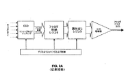
固体デバイスは、一般的にCCD、およびCMOSセンサを含む。これらは、直接、光を感知して、電子的に信号を固体増幅器に送って、その後テレビタイプチューブまたは液晶ディスプレイのようなディスプレイどちらかにイメージを表示することによって、固体デバイスは機能する。図2aおよび図2bは、一般的なCCDセンサについての流れ図および模式図を示している。 Solid state devices typically include CCD and CMOS sensors. They work by solid-state devices by sensing light directly and electronically sending signals to a solid-state amplifier and then displaying the image on either a television-type tube or a display such as a liquid crystal display. 2a and 2b show a flow diagram and schematic diagram for a typical CCD sensor.
CCDおよびCMOSセンサは、固体デバイスである。すなわち、真空のエンベロープはなく、出力はセンサ内ではなく他の場所に表示されるべき電子信号である。固体デバイスは、5−15ボルトの電力で動作する。光は、「s」としてラベルを付けられた個々のピクセル内で感知され、ピクセル格納がレジスタへ読み出されるまで、ピクセルに格納された電子へ変換される。格納レジスタから、複数ピクセルに含まれる電子情報は、次に読み出しレジスタに移され、次に出力増幅器に、次に陰極線管のようなビデオ表示デバイスへ移される。 CCD and CMOS sensors are solid state devices. That is, there is no vacuum envelope and the output is an electronic signal to be displayed elsewhere, not within the sensor. Solid state devices operate with 5-15 volts of power. Light is sensed in individual pixels labeled as “s” and converted to electrons stored in the pixels until the pixel store is read into a register. From the storage register, the electronic information contained in the pixels is then transferred to the readout register, then to the output amplifier, and then to a video display device such as a cathode ray tube.
全ての固体デバイスの不利な点は、乏しい微光レベルパフォーマンス、明るい光源からのポテンシャルブルーミング、乏しい制限された解像度、および高電力消費である。乏しい微光パフォーマンスは、低S/N比という結果になる暗電流および読み出しノイズに起因している。単一ゲイン機構が、読み出しより先に提供された場合、この問題は否定され得る。なぜなら、ノイズ源に打ち勝つ十分な信号が存在するからである。固体デバイスアーキテクチャは、通常読み出しより先の増幅部分を許容しない。乏しく制限された解像度は、大きな信号を収集して、これによりS/N比を増加させようとして通常選択される大きなピクセルサイズに起因する。これらの不利な点は、夜間視界用の固体センサの使用を事実上阻害する。固体デバイスの利点は、特に固体センサがCMOSアレイの場合、イメージインテンシファイアー/I2カメラ、電子読み出しの利点、および低コストと比較するとより良いイメージコントラストである。 The disadvantages of all solid state devices are poor low light level performance, potential blooming from bright light sources, poor limited resolution, and high power consumption. Poor low light performance is due to dark current and readout noise, which results in a low S / N ratio. This problem can be negated if a single gain mechanism is provided prior to readout. This is because there are enough signals to overcome the noise source. Solid state device architectures usually do not allow the amplification part beyond the readout. The poorly limited resolution is due to the large pixel size normally selected to collect large signals and thereby increase the signal-to-noise ratio. These disadvantages effectively hinder the use of solid state sensors for night vision. The advantages of solid state devices are better image contrast compared to image intensifier / I 2 camera, electronic readout advantages, and low cost, especially when the solid state sensor is a CMOS array.
イメージインテンシファイアーおよび固体センサの強みおよび弱みがお互いに補完することで、双方のデバイスの組み合わせは、理論上、より良いパフォーマンスを与え得ると考えられ得る。イメージインテンシファイアー/I2カメラおよび固体センサの代替物として提案された1つのこのような組み合わせは、電子衝撃CCD/CMOSセンサ(EBCCD/CMOS)である。このデバイスは、イメージチューブのフォトカソードおよびボディエンベロープ、およびこのエンベロープに集積されているCCDまたはCMOSセンサのどちらかから成る。EBCCD/CMOSセンサの図示例が図3に示されている。高ボルトが、カソードと固体センサとの間に印加され、そのため生じた電子は、電子衝撃によって固体センサのシリコン内で増幅される。 With the strengths and weaknesses of image intensifiers and solid state sensors complement each other, it can be considered that the combination of both devices can theoretically give better performance. One such combination proposed as an image intensifier / I substitute for 2 cameras and solid sensors are electron impact CCD / CMOS sensor (EBCCD / CMOS). The device consists of an image tube photocathode and body envelope, and either a CCD or CMOS sensor integrated in the envelope. An illustrative example of an EBCCD / CMOS sensor is shown in FIG. A high voltage is applied between the cathode and the solid state sensor so that the generated electrons are amplified in the solid state sensor silicon by electron bombardment.
EBCCD/CMOSデバイスの利点は、電子読み出しを提供することである。しかし、不利な点は多数ある。第1に、シーン内のダイナミックレンジが圧縮される。これは、明るい対象が暗い対象の隣にある場合、シーン内の全体的なコントラストがイメージインテンシファイアー/I2カメラおよび全ての固体デバイスと比較して減少することを意味する。第2に、センサは、固体センサから反射された電子に起因して、明るい光の周りのイメージの「ハロ」の劣化を抱えている。このハロは、正規のイメージチューブ内に存在するが、技術的改良で、ハロが存在しなくなるように減少してきた。第3に、デバイスを動作させるために必要とされる非常に高い電圧(2−10kV)は、シリコン表面にダメージを加えて、やがて性能を劣化させる。 An advantage of EBCCD / CMOS devices is that they provide electronic readout. However, there are a number of disadvantages. First, the dynamic range in the scene is compressed. This is because when a bright subject is next to a dark subject, which means that reduced compared overall contrast in the scene and the image intensifier / I 2 camera and all solid state devices. Second, the sensor has a “halo” degradation of the image around bright light due to electrons reflected from the solid state sensor. This halo is present in regular image tubes, but with technical improvements, it has been reduced to eliminate the halo. Third, the very high voltage (2-10 kV) required to operate the device damages the silicon surface and eventually degrades performance.
それ故、本発明の目的は、イメージインテンシファイアーの最良な機能(良好なS/N比および高対数ゲイン)と、相補的金属酸化物半導体(CMOS)または電荷結合デバイス(CCD)のいずれかの電子的読み出し機能とを組み合わせるインテンシファイハイブリッド固体センサを提供するものである。 Therefore, the object of the present invention is to achieve the best function of an image intensifier (good signal-to-noise ratio and high logarithmic gain) and either complementary metal oxide semiconductor (CMOS) or charge coupled device (CCD). The present invention provides an intensifying hybrid solid-state sensor that combines with the electronic readout function.
(要旨)
本発明は、インテンシファイハイブリッド固体センサを提供する。本発明に従って、固体センサは、イメージインテンシファイカソード、マイクロチャネルプレート(MCP)、およびボディエンベロープでアセンブルされた固体センサを含むイメージデバイスを含む。このデバイスは、イメージインテンシファイアーの最良な機能(良好なS/N比および高対数ゲイン)と、相補的金属酸化物半導体(CMOS)または電荷結合デバイス(CCD)のいずれかの電子的読み出し機能とを組み合わせる。本発明は、少ない光で高感度であり、ゲインが高いことが必要とされる夜間視界システムに主に適用される。
(Summary)
The present invention provides an intensifying hybrid solid state sensor. In accordance with the present invention, a solid state sensor includes an image device that includes an image intensifying cathode, a microchannel plate (MCP), and a solid state sensor assembled with a body envelope. This device has the best image intensifier function (good signal-to-noise ratio and high logarithmic gain) and electronic readout capability of either complementary metal oxide semiconductor (CMOS) or charge coupled device (CCD) And combine. The present invention is mainly applied to a night vision system that requires high sensitivity with little light and high gain.
本発明をより明確に理解するために、添付の図面を参照して、より詳細に本発明を開示する。 For a clearer understanding of the present invention, the present invention will be disclosed in more detail with reference to the accompanying drawings.
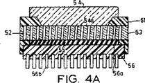
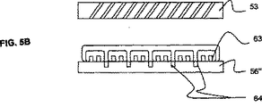
図4Bは、本発明によるインテンシファイハイブリッド固体センサデバイス41の概略図である。センサ41は、標準的イメージチューブフォトカソード54、マイクロチャネルプレート(MCP)53、および固体イメージセンサ56を含む。固体イメージセンサ56は、任意のタイプの固体イメージセンサであり得る。好適には、固体イメージセンサ56は、CCDデバイスである。より好適には、固体イメージセンサ56は、CMOSイメージセンサである。図5Aは、イメージセンサ56’として、背面薄型CCDイメージデバイスを示している。この実施形態において、MCP53は、背面薄型CCDセンサ56’と接続されている。背面薄型CCD56’は、拡散収集エリア56a’および読み出しエリア62のような電子受信表面を含む。図5Bは、標準CCD56’’と接続するMCP53を含む代替の標準CCDイメージデバイスを示す。CCD56’’は、酸化物カバー63および複数の収集ウェル64を含む。図5Cは、CMOS基板56’’’および複数の収集ウェル65を含むCMOSセンサとしてセンサ56を図示する。
FIG. 4B is a schematic diagram of an intensifying hybrid solid
様々な理由のために、CCDによるイメージセンサは、多くの用途において使用が制限されるか、または実用性がない。第1に、CCDは、それらの高いパフォーマンスを達成するために、埋めたチャネルインプラントを有する少なくとも2つのポリシリコンアレイを必要とし、標準的なCMOS製作プロセスを用いてそれらを製作できないことを意味する。第2に、CCDよるイメージャを用いて成し遂げられ得る集積レベルは低い。なぜなら、CCDによるイメージャは、1つの用途において、そのCCDによるイメージャと他のデバイスとを集積するために必要とされるデバイスを含み得ないからである。最終的に、Digital Signal Processor(DSP)および他の画像処理回路等のシステムボード上にある他のデバイスへのイメージアレイからのデータを転送するように用いられる回路は、大きな電気容量を有し、かつ他の回路よりも高い電圧を必要する。これらの電気容量を充電し、かつ放電することに関連する電流は、通常重要であるので、CCDイメージャは、特に、携帯用の、またはバッテリで動作する用途に特に適してはいない。 For various reasons, CCD image sensors are either limited in use or impractical in many applications. First, CCDs require at least two polysilicon arrays with buried channel implants to achieve their high performance, meaning that they cannot be fabricated using standard CMOS fabrication processes. . Second, the level of integration that can be achieved using an imager with a CCD is low. This is because a CCD imager may not include the devices required to integrate the CCD imager with other devices in one application. Finally, the circuits used to transfer data from the image array to other devices on the system board, such as the Digital Signal Processor (DSP) and other image processing circuits, have a large electrical capacitance, And it requires a higher voltage than other circuits. Since the current associated with charging and discharging these capacitances is usually important, CCD imagers are not particularly suitable for portable or battery-operated applications.
例えば、標準のCMOSプロセスを用いた集積回路から製作されたあまり高価ではないイメージセンサが所望される。本質的にCMOSタイプイメージャセンサとともに、発光ダイオード、光トランジスタ、または他の類似のデバイスが、光検出デバイスとして用いられる。光検出素子の出力は、アナログ信号であり、この信号の大きさは、素子が受けた光の量にほぼ比例する。CMOSイメージャは、CCDプロセスによって作られたイメージャと比較すると、より低いパワーを使用し、より低い製作コストを有し、そしてより高いシステム集積を提供するので、いくつかの用途において好ましい。さらに、CMOSイメージャは、論理トランジスタを一般に製造するために通常用いられるプロセスに類似のプロセスを用いて、製造され得るというさらなる利点を有する。本発明の好適な実施形態がイメージセンサ56としてCMOSセンサを組み込んでいるが、任意の固体イメージセンサが機能し、かつ本特許の範囲内にある。
For example, a less expensive image sensor fabricated from an integrated circuit using a standard CMOS process is desired. In essence with CMOS type imager sensors, light emitting diodes, phototransistors, or other similar devices are used as photodetection devices. The output of the light detection element is an analog signal, and the magnitude of this signal is approximately proportional to the amount of light received by the element. CMOS imagers are preferred in some applications because they use lower power, have lower fabrication costs, and provide higher system integration compared to imagers made by the CCD process. Furthermore, CMOS imagers have the additional advantage that they can be manufactured using a process similar to that typically used to manufacture logic transistors. Although the preferred embodiment of the present invention incorporates a CMOS sensor as the
図4Bを再び参照すると、フォトカソード54は、任意の公知のタイプのイメージインテンシファイデバイスで用いられる標準的なフォトカソードであり得る。フォトカソード54は、GaAs、バイアルカリ,InGaAs等の材料であり得るが、これらに制限されない。フォトカソード54は、入力側54aおよび出力側54bを含む。MCP53は、シリコンまたはガラス材料であり得るが、これらに制限されず、好適には、約10〜25mmの厚みである。MCP53は、入力表面49および出力表面50の間に形成された複数のチャネル52を有する。チャネル52は、例えば、円形のプロファイル52’(図6A)、または四角のプロファイル52’’(図6A)の任意のプロファイルのタイプを有し得る。MCP53はイメージセンサ56の電子受信表面56aに接続されている。
Referring again to FIG. 4B, the
好適には、MCP53の出力表面50は、イメージセンサ56の電子受信表面56aに物理的に接触している。しかし、絶縁はMCP53およびイメージセンサ56の間に必要であり得る。従って、薄い絶縁スペーサ55は、MCP53の出力表面50、およびイメージセンサ56の電子受信表面56aの間に挿入され得る。絶縁スペーサ55は、任意の電気的絶縁材料から作られ得、好適には数マイクロより薄い厚さで、イメージセンサ56の電子受信表面56a上に堆積される、薄い層として形成される。例えば、絶縁スペーサは、約10μmの厚さのフィルムであり得るが、これに制限されない。代替的に絶縁スペーサ55は、MCP53の出力表面50上に形成されるフィルム(図示せず)であり得る。
Preferably, the output surface 50 of the
CMOSイメージセンサ56は、電子受信表面56a、および出力56bを含む。MCP53から放射する、増加した多くの電子48は、電子受信表面56aに衝突する。電子受信表面56aは、CMOS基板56’’’、および複数の収集ウェル65(図5C)を含む。収集ウェル65に収集された電子48(図4B参照)は、出力56bを通ってイメージディスプレイデバイス46に送られるインテンシファイイメージ信号を生成する、CMOSセンサ用の標準信号プロセッシング機器を用いて処理される。
電気バイアス回路44は、センサ41へのバイアス電流を提供する。電気バイアス回路44は、第1電気接続42、および第2電気接続43を含む。第1電気接続42は、フォトカソード54およびMCP53の間のバイアス電圧を提供する。第1電気接続42からのバイアス電圧は、EBCCD/CMOSセンサカソードからCCD電圧(すなわち2−10kV)のバイアス電圧よりも小さいように好適にはセットされ得る。例えば、1つの好適なバイアス電圧は、イメージチューブのバイアス電圧(例えば1400Vまで)に類似し得る。第2電気接続43は、MCP53およびCMOSセンサ56の間のバイアス電圧を印加する。好適には、第2電気接続43に印加されたバイアス電圧は、従来技術のデバイス(図1)のイメージチューブ−スクリーン電圧(約4200V)よりも非常に小さい。例えば、第2電気接続43に印加されたバイアス電圧は、100Vまでであり得るが、これに制限されない。図4Aは、センサ41の可能性のある構造を示す。この構造において、フォトカソード54、MCP53、およびイメージセンサ56は、それぞれと物理的に非常に近接し、単一ユニットとして真空のボディまたはエンベロープ61の中に保持される。
The
図4Bを参照すると、動作中にイメージ57からの光58、59は、フォトカソード54の入力側54aを通ってインテンシファイハイブリッド固体センサ41に入射する。フォトカソード54は、入射光を電子48に変化し、その電子48は、フォトカソード54の出力側54bから出力される。フォトカソード54から出る電子48は、MCP53の入力表面49を通ってチャネル52に入射する。電子48がMCP53の入力表面49に照射した後に、第2電子は、MCP53の、複数チャネル52内に生成される。MCP53は、入力表面49を通って入射するそれぞれの電子に対して、チャネル52のそれぞれに数百の電子を生成し得る。それ故、チャネル52から出る電子47の数は、チャネル52に入射する電子48の数より非常に多い。インテンシファイされた数の電子47は、MCP53の出力側50を通ってチャネル52を出て、かつCMOSイメージデバイス56の電子受信表面56aと衝突する。
Referring to FIG. 4B, in operation, light 58 and 59 from
図6は、増加した数の電子47が、チャネル52を出て、かつCMOSイメージセンサ56の特異な収集ウェル65’と衝突する仕方を示す。この図から見て取れるように、収集ウェル65’と電子47を放射するチャネル52の数との間にある関係が存在する。一般的に、MCP53の隣接のチャネル52は、所定のチャネルピッチ52aによって分離される。図6は、1つの収集ウェル65’に対して、複数のチャネル52になるチャネルピッチ52aを示す。
FIG. 6 shows how an increased number of
図7Aから7Cは、本発明によるCMOSウェル/チャネルピッチ関係の3つの異なった代替例を示している。図7Aは、チャネルピッチ52aとCMOS収集ウェル65’との間の1つの関係を示している。この場合、チャネルピッチ52aは、相対的に小さく、一方でCMOSウェル65’のサイズは相対的に大きい。これにより、2以上のチャネル52からのいくつかの電子47がCMOS収集ウェル65’に衝突可能である。図7Bは、他のCMOSウェル/チャネルピッチ関係を示している。この実施形態において、チャネルピッチ52aおよびCMOS収集ウェル65’のサイズは、ほぼ1対1の関係にある。例えば、単一チャネル52からの電子47’は、単一収集ウェル65’に衝突する。図7Cは、他のCMOSウェル/チャネルピッチ関係を示し、チャネルピッチ52aは、相対的に大きく、かつCMOS収集ウェル66のサイズは相対的に小さい。この場合、単一チャネル52からの電子47’’は、複数の収集ウェル66に衝突する。これらの構造のそれぞれが、さまざまな利点を供給する一方、図7Aに示されている関係は本発明に好適である。
Figures 7A-7C illustrate three different alternatives of CMOS well / channel pitch relationships according to the present invention. FIG. 7A shows one relationship between
結果として、インテンシファイハイブリッド固体センサは、他の従来技術のいずれの概念とは異なる条件で動作する。MCP53は、全固体デバイスにコントラストが類似したハイブリッドデバイス(しかし、このデバイスは、低ハロ、良好なS/N比、およびイメージチューブの対数ゲインを有する)を与えるCMOSセンサ56に直接に取り付けられ得る結果になる。動作電圧がさらに低いので、暗い星の光の条件から日中の動作までの動作を許容するイメージチューブのようなハイブリッドデバイスがゲートされ得る。ハイブリッドセンサは、MCP53およびCMOSセンサ56の間の物理的ギャップの欠損から、より良いハロを有する。2つの素子の物理的分離の欠損は、EBCCD/CMOS、またはイメージインテンシファイカメラと比較される場合、コントラストが改善される理由でもある。ハイブリッドデバイスは、イメージチューブの対数ゲイン曲線も有する。EBCCD/CMOSセンサと異なり、ハイブリッドセンサは、低カソード電圧に起因して、ゲートされ得る。
As a result, the intensified hybrid solid state sensor operates under conditions that are different from any other prior art concept. The
本発明の好適な実施形態の上記の詳細な説明は、この出願時で本発明を実行するために発明者によって検討されたベストモードを公開し、例示のためであって、制限のために提供されない。従って、当業者にとって明白な様々な修正および改変は、添付の特許請求の範囲に記載されているように本発明の範囲および意図内であるとみなされる。 The above detailed description of the preferred embodiments of the present invention exposes the best mode considered by the inventors to carry out the present invention at the time of this application, and is provided for purposes of illustration and limitation. Not. Accordingly, various modifications and changes apparent to those skilled in the art are deemed to be within the scope and spirit of the invention as set forth in the appended claims.
Claims (20)
b.該フォトカソードの出力表面に隣接して配置された入力表面と、出力表面と、該入力表面と該出力表面との間で形成された複数のチャネルとを有するマイクロチャネルプレートであって、該マイクロチャネルプレートの該出力表面から増加した数の電子が放射する、マイクロチャネルプレートと、
c.該フォトカソードと該マイクロチャネルプレートとの間に第1バイアス電圧を印加する第1電気接続と、
d.電子受信表面と、インテンシファイイメージ信号を出力する出力とを有する固体イメージデバイスであって、該電子受信表面は、該マイクロチャネルプレートの該出力表面に隣接して配置され、該マイクロチャネルプレートから出力されて増加した数の電子を受ける、固体イメージデバイスと、
e.該マイクロチャネルプレートと固体イメージセンサとの間に第2バイアス電圧を印加する第2電気接続と、
f.該フォトカソードと該マイクロチャネルプレートと該固体イメージデバイスとをユニットとして保持する真空のボディと
を含む、インテンシファイ固体イメージセンサであって、
絶縁層が、該マイクロチャネルプレートの出力表面と、該固体イメージセンサの電子受信表面とを分離し、
該絶縁層は、該マイクロチャネルプレートの出力表面または該固体イメージセンサの該電子受信表面のいずれかの上に配置される厚さの寸法を有する薄い堆積層であり、
該マイクロチャネルプレートの出力表面は、該薄い堆積層の該厚さの寸法と同じ距離だけ、該固体イメージセンサの該電子受信表面から離れている、インテンシファイ固体イメージセンサ。a. A photocathode having an input side and an output side for receiving light from the image, the photocathode from which the electrons generated by the photocathode exit;
b. A microchannel plate having an input surface disposed adjacent to an output surface of the photocathode, an output surface, and a plurality of channels formed between the input surface and the output surface, A microchannel plate that emits an increased number of electrons from the output surface of the channel plate;
c. A first electrical connection for applying a first bias voltage between the photocathode and the microchannel plate;
d. A solid-state image device having an electronic receiving surface and an output for outputting an intensified image signal, the electronic receiving surface being disposed adjacent to the output surface of the microchannel plate and from the microchannel plate receiving a number of electronic with increased output, and a solid imaging device,
e. A second electrical connection for applying a second bias voltage between the microchannel plate and the solid-state image sensor;
f. An intensifying solid-state image sensor comprising: a vacuum body that holds the photocathode, the microchannel plate, and the solid-state image device as a unit;
An insulating layer separates the output surface of the microchannel plate and the electron receiving surface of the solid-state image sensor;
The insulating layer is a thin deposited layer having a thickness dimension disposed on either the output surface of the microchannel plate or the electron receiving surface of the solid-state image sensor;
Intensifying solid-state image sensor, wherein the output surface of the microchannel plate is separated from the electronic receiving surface of the solid-state image sensor by the same distance as the thickness dimension of the thin deposition layer .
b.マイクロチャネルプレートと、
c.該マイクロチャネルプレートから出力された電子を受け、インテンシファイイメージ信号を出力する固体イメージセンサと、
d.該フォトカソード、該マイクロチャネルプレート、および該固体イメージセンサ間に接続される電気バイアス回路と、
e.該フォトカソード、該マイクロチャネルプレート、および該固体イメージセンサを互いに物理的に非常に近接して保持する真空のボディと、
f.該マイクロチャネルプレートの出力表面と、該固体イメージセンサの電子受信表面とを分離する絶縁層と
を含み、
該絶縁層は、該マイクロチャネルプレートの出力表面または該固体イメージセンサの該電子受信表面のいずれかの上に配置される厚さの寸法を有する薄い堆積層であり、
該マイクロチャネルプレートの出力表面は、該薄い堆積層の該厚さの寸法と同じ距離だけ、該固体イメージセンサの該電子受信表面から離れている、インテンシファイ固体イメージセンサ。a. A photocathode;
b. A microchannel plate;
c. A solid-state image sensor that receives electrons output from the microchannel plate and outputs an intensified image signal;
d. An electrical bias circuit connected between the photocathode, the microchannel plate, and the solid state image sensor;
e. A vacuum body that holds the photocathode, the microchannel plate, and the solid state image sensor in close physical proximity to each other;
f. An insulating layer separating the output surface of the microchannel plate and the electron receiving surface of the solid-state image sensor;
The insulating layer is a thin deposited layer having a thickness dimension disposed on either the output surface of the microchannel plate or the electron receiving surface of the solid-state image sensor;
Intensifying solid-state image sensor, wherein the output surface of the microchannel plate is separated from the electronic receiving surface of the solid-state image sensor by the same distance as the thickness dimension of the thin deposition layer .
b.該フォトカソードの出力表面に接続される電子増倍デバイスであって、該フォトカソードから電子を受け、該受けた電子の数を増加させ、増加した数の電子を出力するように適合されている電子増倍デバイスと、
c.固体イメージセンサであって、
i.該電子増倍デバイスに接続された複数の収集ウェルであって、該電子増倍デバイスから出力された該増加した数の電子を受け、インテンシファイイメージ信号を生成する複数の収集ウェルと、
ii.ディスプレイデバイスに該インテンシファイイメージ信号を出力する出力と
をさらに含む固体イメージセンサと、
d.該フォトカソードと該固体イメージセンサとの間に接続された電子回路であって、少なくとも1つのバイアス電圧を該フォトカソードと該固体イメージセンサとの間に印加する電子回路と、
e.該フォトカソード、該電子増倍デバイス、および該固体イメージセンサが少なくとも部分的真空に保たれているボディと、
f.該電子増倍デバイスの出力表面と、該固体イメージセンサの電子受信表面とを分離する絶縁層と
を含み、
該絶縁層は、該マイクロチャネルプレートの出力表面または該固体イメージセンサの該電子受信表面のいずれかの上に配置される厚さの寸法を有する薄い堆積層であり、
該マイクロチャネルプレートの出力表面は、該薄い堆積層の該厚さの寸法と同じ距離だけ、該固体イメージセンサの該電子受信表面から離れている、インテンシファイ固体イメージセンサ。a. A photocathode that converts light from the image into electrons,
b. An electron multiplication device connected to the output surface of the photocathode, adapted to receive electrons from the photocathode, increase the number of received electrons, and output an increased number of electrons An electron multiplier device;
c. A solid-state image sensor,
i. A plurality of collection wells connected to the electron multiplier device, the collection wells receiving the increased number of electrons output from the electron multiplier device and generating an intensified image signal;
ii. A solid-state image sensor further comprising: an output for outputting the intensified image signal to a display device;
d. An electronic circuit connected between the photocathode and the solid-state image sensor, the electronic circuit applying at least one bias voltage between the photocathode and the solid-state image sensor;
e. A body in which the photocathode, the electron multiplier device, and the solid state image sensor are kept at least partially in vacuum;
f. An insulating layer separating the output surface of the electron multiplier device and the electron receiving surface of the solid-state image sensor;
The insulating layer is a thin deposited layer having a thickness dimension disposed on either the output surface of the microchannel plate or the electron receiving surface of the solid-state image sensor;
Intensifying solid-state image sensor, wherein the output surface of the microchannel plate is separated from the electronic receiving surface of the solid-state image sensor by a distance equal to the thickness dimension of the thin deposition layer .
Applications Claiming Priority (2)
| Application Number | Priority Date | Filing Date | Title |
|---|---|---|---|
| US09/973,907 US6747258B2 (en) | 2001-10-09 | 2001-10-09 | Intensified hybrid solid-state sensor with an insulating layer |
| PCT/US2002/032101 WO2003032358A1 (en) | 2001-10-09 | 2002-10-09 | Intensified hybrid solid-state sensor |
Publications (2)
| Publication Number | Publication Date |
|---|---|
| JP2005506657A JP2005506657A (en) | 2005-03-03 |
| JP4310190B2 true JP4310190B2 (en) | 2009-08-05 |
Family
ID=25521360
Family Applications (1)
| Application Number | Title | Priority Date | Filing Date |
|---|---|---|---|
| JP2003535229A Expired - Fee Related JP4310190B2 (en) | 2001-10-09 | 2002-10-09 | Intensify hybrid solid state sensor |
Country Status (10)
| Country | Link |
|---|---|
| US (1) | US6747258B2 (en) |
| EP (1) | EP1436825B1 (en) |
| JP (1) | JP4310190B2 (en) |
| KR (1) | KR20040050897A (en) |
| CN (1) | CN100397548C (en) |
| AU (1) | AU2002334903B2 (en) |
| CA (1) | CA2458532C (en) |
| DE (1) | DE60236744D1 (en) |
| RU (1) | RU2297070C2 (en) |
| WO (1) | WO2003032358A1 (en) |
Families Citing this family (67)
| Publication number | Priority date | Publication date | Assignee | Title |
|---|---|---|---|---|
| US7015452B2 (en) * | 2001-10-09 | 2006-03-21 | Itt Manufacturing Enterprises, Inc. | Intensified hybrid solid-state sensor |
| US6747258B2 (en) | 2001-10-09 | 2004-06-08 | Itt Manufacturing Enterprises, Inc. | Intensified hybrid solid-state sensor with an insulating layer |
| US6747821B2 (en) * | 2002-06-12 | 2004-06-08 | Litton Systems, Inc. | Method and system for mounting a detector |
| US7092013B2 (en) * | 2002-06-12 | 2006-08-15 | Litton Systems, Inc. | InGaAs image intensifier camera |
| US7274830B2 (en) * | 2002-06-12 | 2007-09-25 | Litton Systems, Inc. | System for multi-sensor image fusion |
| US6970190B2 (en) * | 2002-06-12 | 2005-11-29 | Litton Systems, Inc. | Event synchronization for detector systems |
| IL165053A0 (en) * | 2002-06-12 | 2005-12-18 | Litton Systems Inc | Image intensification camera |
| US7023126B2 (en) * | 2003-12-03 | 2006-04-04 | Itt Manufacturing Enterprises Inc. | Surface structures for halo reduction in electron bombarded devices |
| JP4931793B2 (en) * | 2004-03-05 | 2012-05-16 | オイ コーポレイション | Mass spectrometer focal plane detector assembly |
| US7012328B2 (en) * | 2004-05-14 | 2006-03-14 | Intevac, Inc. | Semiconductor die attachment for high vacuum tubes |
| US7607560B2 (en) * | 2004-05-14 | 2009-10-27 | Intevac, Inc. | Semiconductor die attachment for high vacuum tubes |
| US7051469B1 (en) * | 2004-12-14 | 2006-05-30 | Omnitech Partners | Night sight for use with a telescopic sight |
| US7275343B2 (en) * | 2005-02-16 | 2007-10-02 | Leupold & Stevens, Inc. | Riflescope with recessed bottom surface for reduced mounting height |
| US7235768B1 (en) | 2005-02-28 | 2007-06-26 | United States Of America As Represented By The Secretary Of The Air Force | Solid state vision enhancement device |
| US7333270B1 (en) * | 2005-06-10 | 2008-02-19 | Omnitech Partners | Dual band night vision device |
| US20070223087A1 (en) * | 2005-06-24 | 2007-09-27 | Omnitech Partners | Combined day and night weapon sight |
| US7482571B2 (en) * | 2005-08-01 | 2009-01-27 | Itt Manufacturing Enterprises, Inc. | Low cost planar image intensifier tube structure |
| JP4491391B2 (en) * | 2005-08-05 | 2010-06-30 | 株式会社日立ハイテクノロジーズ | Defect inspection apparatus and defect inspection method |
| IL176694A0 (en) * | 2006-07-04 | 2006-10-31 | Univ Ramot | Method and device for low light level imaging |
| US7687759B2 (en) * | 2007-11-27 | 2010-03-30 | Itt Manufacturing Enterprises, Inc. | Slotted microchannel plate (MCP) |
| US8119971B2 (en) | 2008-01-17 | 2012-02-21 | Ball Corporation | Pulse data recorder in which a value held by a bit of a memory is determined by a state of a switch |
| US8077294B1 (en) | 2008-01-17 | 2011-12-13 | Ball Aerospace & Technologies Corp. | Optical autocovariance lidar |
| FR2929001B1 (en) * | 2008-03-18 | 2010-03-05 | Thales Sa | HYBRID EBCMOS-TYPE ULTRAVIOLET RADIATION DETECTION DEVICE COMPRISING A SOLAR-RADIATION-INSENSITIVE MEMBRANE |
| US9041915B2 (en) | 2008-05-09 | 2015-05-26 | Ball Aerospace & Technologies Corp. | Systems and methods of scene and action capture using imaging system incorporating 3D LIDAR |
| US7961301B2 (en) * | 2008-05-09 | 2011-06-14 | Ball Aerospace & Technologies Corp. | Flash LADAR system |
| US7880127B2 (en) * | 2008-10-27 | 2011-02-01 | Itt Manufacturing Enterprises, Inc. | Apparatus and method for aligning an image sensor including a header alignment means |
| US7880128B2 (en) * | 2008-10-27 | 2011-02-01 | Itt Manufacturing Enterprises, Inc. | Vented header assembly of an image intensifier device |
| US8071932B2 (en) * | 2008-10-27 | 2011-12-06 | Itt Manufacturing Enterprises, Inc. | Apparatus and method for sealing an image intensifier device |
| US7929215B1 (en) | 2009-02-20 | 2011-04-19 | Ball Aerospace & Technologies Corp. | Field widening lens |
| DE102009021136A1 (en) * | 2009-05-13 | 2010-12-16 | Fraunhofer-Gesellschaft zur Förderung der angewandten Forschung e.V. | control device |
| JPWO2011016420A1 (en) * | 2009-08-03 | 2013-01-10 | 株式会社エヌ・ピー・シー | Solar cell defect inspection apparatus, defect inspection method, and program |
| US8306273B1 (en) | 2009-12-28 | 2012-11-06 | Ball Aerospace & Technologies Corp. | Method and apparatus for LIDAR target identification and pose estimation |
| US8736818B2 (en) | 2010-08-16 | 2014-05-27 | Ball Aerospace & Technologies Corp. | Electronically steered flash LIDAR |
| US8902523B2 (en) | 2011-04-27 | 2014-12-02 | Kenneth JAMISON | Systems and methods for utilizing imperfectly manufactured image intensifier tubes in night vision systems |
| US10197501B2 (en) | 2011-12-12 | 2019-02-05 | Kla-Tencor Corporation | Electron-bombarded charge-coupled device and inspection systems using EBCCD detectors |
| US20130201316A1 (en) | 2012-01-09 | 2013-08-08 | May Patents Ltd. | System and method for server based control |
| US8744126B1 (en) | 2012-03-07 | 2014-06-03 | Ball Aerospace & Technologies Corp. | Morphology based hazard detection |
| US9496425B2 (en) | 2012-04-10 | 2016-11-15 | Kla-Tencor Corporation | Back-illuminated sensor with boron layer |
| US9601299B2 (en) | 2012-08-03 | 2017-03-21 | Kla-Tencor Corporation | Photocathode including silicon substrate with boron layer |
| US9426400B2 (en) | 2012-12-10 | 2016-08-23 | Kla-Tencor Corporation | Method and apparatus for high speed acquisition of moving images using pulsed illumination |
| US9478402B2 (en) | 2013-04-01 | 2016-10-25 | Kla-Tencor Corporation | Photomultiplier tube, image sensor, and an inspection system using a PMT or image sensor |
| US9177764B1 (en) * | 2013-11-11 | 2015-11-03 | Exelis, Inc. | Image intensifier having an ion barrier with conductive material and method for making the same |
| CN103645391B (en) * | 2013-12-03 | 2016-03-02 | 中国科学院空间科学与应用研究中心 | A kind of metering circuit of micro channel plate gain and method |
| US9347890B2 (en) | 2013-12-19 | 2016-05-24 | Kla-Tencor Corporation | Low-noise sensor and an inspection system using a low-noise sensor |
| US9748294B2 (en) | 2014-01-10 | 2017-08-29 | Hamamatsu Photonics K.K. | Anti-reflection layer for back-illuminated sensor |
| US9410901B2 (en) | 2014-03-17 | 2016-08-09 | Kla-Tencor Corporation | Image sensor, an inspection system and a method of inspecting an article |
| US9460886B2 (en) * | 2014-07-22 | 2016-10-04 | Kla-Tencor Corporation | High resolution high quantum efficiency electron bombarded CCD or CMOS imaging sensor |
| US9767986B2 (en) | 2014-08-29 | 2017-09-19 | Kla-Tencor Corporation | Scanning electron microscope and methods of inspecting and reviewing samples |
| CN105609511B (en) * | 2014-11-21 | 2019-01-15 | 中国科学院微电子研究所 | A kind of single photon image detector and its manufacturing method |
| US9860466B2 (en) | 2015-05-14 | 2018-01-02 | Kla-Tencor Corporation | Sensor with electrically controllable aperture for inspection and metrology systems |
| US10748730B2 (en) | 2015-05-21 | 2020-08-18 | Kla-Tencor Corporation | Photocathode including field emitter array on a silicon substrate with boron layer |
| RU2622397C2 (en) * | 2015-08-10 | 2017-06-15 | Открытое акционерное общество "Центральный научно-исследовательский институт "Электрон" | High-voltage hybrid photosensitive device for detecting low-intensity radiation |
| US10462391B2 (en) | 2015-08-14 | 2019-10-29 | Kla-Tencor Corporation | Dark-field inspection using a low-noise sensor |
| WO2017058901A1 (en) | 2015-09-28 | 2017-04-06 | Ball Aerospace & Technologies Corp. | Differential absorption lidar |
| US10778925B2 (en) | 2016-04-06 | 2020-09-15 | Kla-Tencor Corporation | Multiple column per channel CCD sensor architecture for inspection and metrology |
| US10313622B2 (en) | 2016-04-06 | 2019-06-04 | Kla-Tencor Corporation | Dual-column-parallel CCD sensor and inspection systems using a sensor |
| CN106876229B (en) * | 2016-12-30 | 2018-05-29 | 中国科学院西安光学精密机械研究所 | A kind of contact conductor unit, vacuum photoelectric device and preparation method thereof |
| EP3652721A1 (en) | 2017-09-04 | 2020-05-20 | NNG Software Developing and Commercial LLC | A method and apparatus for collecting and using sensor data from a vehicle |
| US10921245B2 (en) | 2018-06-08 | 2021-02-16 | Ball Aerospace & Technologies Corp. | Method and systems for remote emission detection and rate determination |
| CN108848326B (en) * | 2018-06-13 | 2021-01-01 | 吉林大学 | Front-end reading circuit of high dynamic range MCP detector and reading method thereof |
| US11114489B2 (en) | 2018-06-18 | 2021-09-07 | Kla-Tencor Corporation | Back-illuminated sensor and a method of manufacturing a sensor |
| WO2020035852A2 (en) | 2018-08-14 | 2020-02-20 | Neurotrigger Ltd. | Method and apparatus for transcutaneous facial nerve stimulation and applications thereof |
| US10943760B2 (en) | 2018-10-12 | 2021-03-09 | Kla Corporation | Electron gun and electron microscope |
| CN109547718B (en) * | 2018-12-04 | 2020-11-27 | 北方夜视技术股份有限公司 | Miniaturized high-gain low-illumination night vision imaging device |
| US11114491B2 (en) | 2018-12-12 | 2021-09-07 | Kla Corporation | Back-illuminated sensor and a method of manufacturing a sensor |
| EP3888346A4 (en) | 2019-02-19 | 2022-08-24 | Edgy Bees Ltd. | Estimating real-time delay of a video data stream |
| US11848350B2 (en) | 2020-04-08 | 2023-12-19 | Kla Corporation | Back-illuminated sensor and a method of manufacturing a sensor using a silicon on insulator wafer |
Family Cites Families (30)
| Publication number | Priority date | Publication date | Assignee | Title |
|---|---|---|---|---|
| US4471378A (en) | 1979-12-31 | 1984-09-11 | American Sterilizer Company | Light and particle image intensifier |
| FR2494906A1 (en) | 1980-11-25 | 1982-05-28 | Thomson Csf | ELECTRON MULTIPLICATION PHOTODETECTOR TUBE FOR USE IN A COLOR VIDEO READER |
| US4355229A (en) | 1980-11-28 | 1982-10-19 | Rca Corporation | Intensified charge coupled image sensor having universal header assembly |
| US4395636A (en) | 1980-12-24 | 1983-07-26 | Regents Of The University Of California | Radiation imaging apparatus |
| US4555731A (en) | 1984-04-30 | 1985-11-26 | Polaroid Corporation | Electronic imaging camera with microchannel plate |
| IL72878A (en) | 1984-09-06 | 1988-10-31 | Tadiran Ltd | Reconnaissance system |
| CN1003102B (en) * | 1986-05-13 | 1989-01-18 | 西安应用光学研究所 | Second-generation zoom image intensifie tube |
| JPH0775407B2 (en) * | 1988-05-17 | 1995-08-09 | 日本放送協会 | Imaging device |
| JPH0775408B2 (en) * | 1988-05-17 | 1995-08-09 | 日本放送協会 | Imaging device |
| US5099128A (en) | 1989-03-17 | 1992-03-24 | Roger Stettner | High resolution position sensitive detector |
| US5084780A (en) | 1989-09-12 | 1992-01-28 | Itt Corporation | Telescopic sight for day/night viewing |
| US5029963A (en) | 1990-02-15 | 1991-07-09 | Itt Corporation | Replacement device for a driver's viewer |
| US5218194A (en) | 1991-08-19 | 1993-06-08 | Varo Inc. | Advanced high voltage power supply for night vision image intensifer |
| DE4237097A1 (en) | 1991-11-19 | 1993-05-27 | Siemens Ag | X=ray image intensifier with vacuum housing having input light screening - has input window of vacuum housing and photocathode optically coupled on one side of glass carrier and electron multiplying stage |
| US5349177A (en) | 1993-02-22 | 1994-09-20 | Itt Corporation | Image intensifier tube having a solid state electron amplifier |
| CN1086347A (en) * | 1993-03-04 | 1994-05-04 | 中国科学院西安光学精密机械研究所 | A kind of double close-up framming image intensifier |
| US5665959A (en) | 1995-01-13 | 1997-09-09 | The United States Of America As Represented By The Administrator Of The National Aeronautics And Space Adminstration | Solid-state image sensor with focal-plane digital photon-counting pixel array |
| US6069352A (en) | 1997-09-09 | 2000-05-30 | Interscience, Inc. | Intensity control system for intensified imaging systems |
| JP4173575B2 (en) | 1998-01-16 | 2008-10-29 | 浜松ホトニクス株式会社 | Imaging device |
| US6072565A (en) | 1998-05-18 | 2000-06-06 | Litton Systems, Inc. | Night vision device with improved laser range finder |
| US6271511B1 (en) | 1999-02-22 | 2001-08-07 | Litton Systems, Inc. | High-resolution night vision device with image intensifier tube, optimized high-resolution MCP, and method |
| DE19927694C1 (en) | 1999-06-17 | 2000-11-02 | Lutz Fink | Semiconductor sensor with pixel structure e.g. for optoelectronic image sensor has overall conductive layer provided with gaps between individual pixel elements filled with relatively insulated conductive layer |
| US6285018B1 (en) | 1999-07-20 | 2001-09-04 | Intevac, Inc. | Electron bombarded active pixel sensor |
| US6333205B1 (en) * | 1999-08-16 | 2001-12-25 | Micron Technology, Inc. | CMOS imager with selectively silicided gates |
| US6303918B1 (en) | 1999-08-25 | 2001-10-16 | Litton Systems, Inc. | Method and system for detecting radiation incorporating a hardened photocathode |
| US6278104B1 (en) | 1999-09-30 | 2001-08-21 | Litton Systems, Inc. | Power supply for night viewers |
| US6492657B1 (en) | 2000-01-27 | 2002-12-10 | Burle Technologies, Inc. | Integrated semiconductor microchannel plate and planar diode electron flux amplifier and collector |
| DE10014311C2 (en) | 2000-03-23 | 2003-08-14 | Siemens Ag | radiation converter |
| CN2441277Y (en) * | 2000-09-07 | 2001-08-01 | 中国科学院长春光学精密机械与物理研究所 | Optical fiber type X-ray image enhanced sensor |
| US6747258B2 (en) | 2001-10-09 | 2004-06-08 | Itt Manufacturing Enterprises, Inc. | Intensified hybrid solid-state sensor with an insulating layer |
-
2001
- 2001-10-09 US US09/973,907 patent/US6747258B2/en not_active Expired - Lifetime
-
2002
- 2002-10-09 CN CNB028199774A patent/CN100397548C/en not_active Expired - Fee Related
- 2002-10-09 EP EP02800954A patent/EP1436825B1/en not_active Expired - Fee Related
- 2002-10-09 AU AU2002334903A patent/AU2002334903B2/en not_active Ceased
- 2002-10-09 RU RU2004113949/09A patent/RU2297070C2/en not_active IP Right Cessation
- 2002-10-09 KR KR10-2004-7004218A patent/KR20040050897A/en not_active Application Discontinuation
- 2002-10-09 WO PCT/US2002/032101 patent/WO2003032358A1/en active IP Right Grant
- 2002-10-09 CA CA2458532A patent/CA2458532C/en not_active Expired - Fee Related
- 2002-10-09 DE DE60236744T patent/DE60236744D1/en not_active Expired - Lifetime
- 2002-10-09 JP JP2003535229A patent/JP4310190B2/en not_active Expired - Fee Related
Also Published As
| Publication number | Publication date |
|---|---|
| EP1436825A1 (en) | 2004-07-14 |
| US20030066951A1 (en) | 2003-04-10 |
| JP2005506657A (en) | 2005-03-03 |
| WO2003032358A1 (en) | 2003-04-17 |
| RU2004113949A (en) | 2005-09-20 |
| RU2297070C2 (en) | 2007-04-10 |
| CA2458532C (en) | 2010-11-30 |
| EP1436825B1 (en) | 2010-06-16 |
| CN100397548C (en) | 2008-06-25 |
| CA2458532A1 (en) | 2003-04-17 |
| DE60236744D1 (en) | 2010-07-29 |
| US6747258B2 (en) | 2004-06-08 |
| AU2002334903B2 (en) | 2007-03-01 |
| KR20040050897A (en) | 2004-06-17 |
| CN1568532A (en) | 2005-01-19 |
Similar Documents
| Publication | Publication Date | Title |
|---|---|---|
| JP4310190B2 (en) | Intensify hybrid solid state sensor | |
| US7015452B2 (en) | Intensified hybrid solid-state sensor | |
| AU2002334903A1 (en) | Intensified hybrid solid-state sensor | |
| JP5430810B2 (en) | Electron impact active pixel sensor | |
| US6307586B1 (en) | Electron bombarded active pixel sensor camera incorporating gain control | |
| US6657178B2 (en) | Electron bombarded passive pixel sensor imaging | |
| US20210335587A1 (en) | Global shutter for transmission mode secondary electron intensifier by a low voltage signal | |
| CN109547718B (en) | Miniaturized high-gain low-illumination night vision imaging device | |
| US20210335566A1 (en) | Electronically addressable display incorporated into a transmission mode secondary electron image intensifier | |
| JP3021388B2 (en) | A device that converts infrared images into visible light images | |
| JPH076715A (en) | Planar type picture amplifier |
Legal Events
| Date | Code | Title | Description |
|---|---|---|---|
| A621 | Written request for application examination |
Free format text: JAPANESE INTERMEDIATE CODE: A621 Effective date: 20050913 |
|
| A131 | Notification of reasons for refusal |
Free format text: JAPANESE INTERMEDIATE CODE: A131 Effective date: 20080624 |
|
| A601 | Written request for extension of time |
Free format text: JAPANESE INTERMEDIATE CODE: A601 Effective date: 20080924 |
|
| A602 | Written permission of extension of time |
Free format text: JAPANESE INTERMEDIATE CODE: A602 Effective date: 20081001 |
|
| A521 | Request for written amendment filed |
Free format text: JAPANESE INTERMEDIATE CODE: A523 Effective date: 20081016 |
|
| A131 | Notification of reasons for refusal |
Free format text: JAPANESE INTERMEDIATE CODE: A131 Effective date: 20081112 |
|
| A521 | Request for written amendment filed |
Free format text: JAPANESE INTERMEDIATE CODE: A523 Effective date: 20090113 |
|
| A131 | Notification of reasons for refusal |
Free format text: JAPANESE INTERMEDIATE CODE: A131 Effective date: 20090209 |
|
| A521 | Request for written amendment filed |
Free format text: JAPANESE INTERMEDIATE CODE: A523 Effective date: 20090327 |
|
| TRDD | Decision of grant or rejection written | ||
| A01 | Written decision to grant a patent or to grant a registration (utility model) |
Free format text: JAPANESE INTERMEDIATE CODE: A01 Effective date: 20090422 |
|
| A01 | Written decision to grant a patent or to grant a registration (utility model) |
Free format text: JAPANESE INTERMEDIATE CODE: A01 |
|
| A61 | First payment of annual fees (during grant procedure) |
Free format text: JAPANESE INTERMEDIATE CODE: A61 Effective date: 20090511 |
|
| R150 | Certificate of patent or registration of utility model |
Free format text: JAPANESE INTERMEDIATE CODE: R150 |
|
| FPAY | Renewal fee payment (event date is renewal date of database) |
Free format text: PAYMENT UNTIL: 20120515 Year of fee payment: 3 |
|
| LAPS | Cancellation because of no payment of annual fees |