JP4290177B2 - Mold, alignment method, pattern forming apparatus, pattern transfer apparatus, and chip manufacturing method - Google Patents
Mold, alignment method, pattern forming apparatus, pattern transfer apparatus, and chip manufacturing method Download PDFInfo
- Publication number
- JP4290177B2 JP4290177B2 JP2006137319A JP2006137319A JP4290177B2 JP 4290177 B2 JP4290177 B2 JP 4290177B2 JP 2006137319 A JP2006137319 A JP 2006137319A JP 2006137319 A JP2006137319 A JP 2006137319A JP 4290177 B2 JP4290177 B2 JP 4290177B2
- Authority
- JP
- Japan
- Prior art keywords
- mold
- mark
- alignment
- pattern
- workpiece
- Prior art date
- Legal status (The legal status is an assumption and is not a legal conclusion. Google has not performed a legal analysis and makes no representation as to the accuracy of the status listed.)
- Active
Links
Images


Classifications
-
- B—PERFORMING OPERATIONS; TRANSPORTING
- B81—MICROSTRUCTURAL TECHNOLOGY
- B81C—PROCESSES OR APPARATUS SPECIALLY ADAPTED FOR THE MANUFACTURE OR TREATMENT OF MICROSTRUCTURAL DEVICES OR SYSTEMS
- B81C1/00—Manufacture or treatment of devices or systems in or on a substrate
- B81C1/00436—Shaping materials, i.e. techniques for structuring the substrate or the layers on the substrate
- B81C1/00444—Surface micromachining, i.e. structuring layers on the substrate
- B81C1/0046—Surface micromachining, i.e. structuring layers on the substrate using stamping, e.g. imprinting
-
- B—PERFORMING OPERATIONS; TRANSPORTING
- B82—NANOTECHNOLOGY
- B82Y—SPECIFIC USES OR APPLICATIONS OF NANOSTRUCTURES; MEASUREMENT OR ANALYSIS OF NANOSTRUCTURES; MANUFACTURE OR TREATMENT OF NANOSTRUCTURES
- B82Y10/00—Nanotechnology for information processing, storage or transmission, e.g. quantum computing or single electron logic
-
- B—PERFORMING OPERATIONS; TRANSPORTING
- B82—NANOTECHNOLOGY
- B82Y—SPECIFIC USES OR APPLICATIONS OF NANOSTRUCTURES; MEASUREMENT OR ANALYSIS OF NANOSTRUCTURES; MANUFACTURE OR TREATMENT OF NANOSTRUCTURES
- B82Y40/00—Manufacture or treatment of nanostructures
-
- G—PHYSICS
- G03—PHOTOGRAPHY; CINEMATOGRAPHY; ANALOGOUS TECHNIQUES USING WAVES OTHER THAN OPTICAL WAVES; ELECTROGRAPHY; HOLOGRAPHY
- G03F—PHOTOMECHANICAL PRODUCTION OF TEXTURED OR PATTERNED SURFACES, e.g. FOR PRINTING, FOR PROCESSING OF SEMICONDUCTOR DEVICES; MATERIALS THEREFOR; ORIGINALS THEREFOR; APPARATUS SPECIALLY ADAPTED THEREFOR
- G03F7/00—Photomechanical, e.g. photolithographic, production of textured or patterned surfaces, e.g. printing surfaces; Materials therefor, e.g. comprising photoresists; Apparatus specially adapted therefor
- G03F7/0002—Lithographic processes using patterning methods other than those involving the exposure to radiation, e.g. by stamping
-
- G—PHYSICS
- G03—PHOTOGRAPHY; CINEMATOGRAPHY; ANALOGOUS TECHNIQUES USING WAVES OTHER THAN OPTICAL WAVES; ELECTROGRAPHY; HOLOGRAPHY
- G03F—PHOTOMECHANICAL PRODUCTION OF TEXTURED OR PATTERNED SURFACES, e.g. FOR PRINTING, FOR PROCESSING OF SEMICONDUCTOR DEVICES; MATERIALS THEREFOR; ORIGINALS THEREFOR; APPARATUS SPECIALLY ADAPTED THEREFOR
- G03F9/00—Registration or positioning of originals, masks, frames, photographic sheets or textured or patterned surfaces, e.g. automatically
- G03F9/70—Registration or positioning of originals, masks, frames, photographic sheets or textured or patterned surfaces, e.g. automatically for microlithography
- G03F9/7073—Alignment marks and their environment
- G03F9/7076—Mark details, e.g. phase grating mark, temporary mark
-
- G—PHYSICS
- G03—PHOTOGRAPHY; CINEMATOGRAPHY; ANALOGOUS TECHNIQUES USING WAVES OTHER THAN OPTICAL WAVES; ELECTROGRAPHY; HOLOGRAPHY
- G03F—PHOTOMECHANICAL PRODUCTION OF TEXTURED OR PATTERNED SURFACES, e.g. FOR PRINTING, FOR PROCESSING OF SEMICONDUCTOR DEVICES; MATERIALS THEREFOR; ORIGINALS THEREFOR; APPARATUS SPECIALLY ADAPTED THEREFOR
- G03F9/00—Registration or positioning of originals, masks, frames, photographic sheets or textured or patterned surfaces, e.g. automatically
- G03F9/70—Registration or positioning of originals, masks, frames, photographic sheets or textured or patterned surfaces, e.g. automatically for microlithography
- G03F9/7073—Alignment marks and their environment
- G03F9/7084—Position of mark on substrate, i.e. position in (x, y, z) of mark, e.g. buried or resist covered mark, mark on rearside, at the substrate edge, in the circuit area, latent image mark, marks in plural levels
Abstract
Description
本発明は、凹凸パターンを形成するために用いられるモールド、アライメント方法、パターン形成装置、パターン転写装置、及びチップの製造方法に関し、より詳しくは、当該モールドと基板との位置合わせ技術に関するものである。 The present invention is a mold, the alignment process used to form an uneven pattern, pattern forming apparatus, a pattern transfer apparatus, and relates to a manufacturing method of the chip, and more particularly, relates to the alignment technique of the mold and the substrate is there.
近年、モールド上の微細なパターン構造を、樹脂や金属等の部材に加圧転写する微細加工技術が開発されている。
この技術は、ナノインプリントあるいはナノエンボッシングと呼ばれ、数nmオーダーの分解能が期待されるため、ステッパ、スキャナ等の光露光装置に代わる次世代の半導体製造技術として注目を集めている。
また、ナノインプリントは、サイズにも依るが、ウエハ上に立体構造が一括形成可能であり、フォトニッククリスタル等の光学素子や、μ−TAS(Micro Total Analysis System)等のバイオチップの製造技術への応用が期待される。
2. Description of the Related Art In recent years, a microfabrication technique has been developed that press-transfers a fine pattern structure on a mold to a member such as resin or metal.
This technique is called nanoimprinting or nano-embossing, and is expected to have a resolution of the order of several nanometers. Therefore, this technique is attracting attention as a next-generation semiconductor manufacturing technique that can replace optical exposure apparatuses such as steppers and scanners.
In addition, nanoimprints can form a three-dimensional structure on a wafer at a time, depending on the size, and can be applied to optical elements such as photonic crystals and biochip manufacturing technologies such as μ-TAS (Micro Total Analysis System). Application is expected.
例えば、非特許文献1には、インプリントによる加工を半導体の製造に適用する場合が示されている。つまり、ワーク(半導体ウエハ)上に光硬化樹脂層を形成し、当該樹脂に所望の凹凸パターンを有するモールドを押し当て、さらに加圧し、光を照射することで樹脂を硬化させる。
こうして、前記樹脂層が硬化する結果、モールドの凹凸パターンが転写されるので、この硬化した樹脂層をマスクとしてエッチング等を行えば、半導体ウエハへのパターン形成が実現される。
As a result of the curing of the resin layer, the concavo-convex pattern of the mold is transferred. If etching or the like is performed using the cured resin layer as a mask, pattern formation on the semiconductor wafer is realized.
インプリント技術においては、パターン転写の際の、モールドとワークとの位置合わせを精密に行う必要がある。
一般的には、モールド側に設けられている位置合わせ構造(以下、アライメントマークと記載する場合がある。)と、半導体ウエハなどのワークに設けられているアライメントマークとを、モールド側から光学的に読取ることにより位置合わせを行う。
In the imprint technique, it is necessary to precisely align the mold and the workpiece during pattern transfer.
In general, an alignment structure provided on the mold side (hereinafter sometimes referred to as an alignment mark) and an alignment mark provided on a workpiece such as a semiconductor wafer are optically connected from the mold side. Alignment is performed by reading the data.
しかしながら、モールドとワークとの間に、モールドのパターンが転写される樹脂が介在する場合、次の問題が生じる場合がある。
すなわち、モールド側のアライメントマークに前記樹脂が接触することにより、当該アライメントマークの見え方が不鮮明になったりする場合がある。そして、当該モールドと樹脂との屈折率差が十分でない場合には、特に見え難くなる場合がある。
However, when a resin to which a pattern of the mold is transferred is interposed between the mold and the workpiece, the following problem may occur.
That is, when the resin comes into contact with the alignment mark on the mold side, the appearance of the alignment mark may become unclear. And when the refractive index difference between the mold and the resin is not sufficient, it may be particularly difficult to see.
そこで、本発明は、上記課題を解決し、モールドとワークとの高精度な位置合わせに適用される新規なモールド、当該モールドを用いたアライメント方法、
係るパターン形成を行うためのパターン形成装置、パターン転写装置、及びチップの製造方法を提供することを目的とする。
Then, this invention solves the said subject, the novel mold applied to highly accurate position alignment with a mold and a workpiece | work, the alignment method using the said mold,
An object of the present invention is to provide a pattern forming apparatus , a pattern transfer apparatus, and a chip manufacturing method for performing such pattern formation.
本発明は上記課題を解決するため、次のように構成したモールド、アライメント方法、パターン形成装置、パターン転写装置、及びチップの製造方法を提供するものである。
本発明のモールドは、
転写するためのパターン領域を有する第1の面と、
前記第1の面と反対側に位置する第2の面と、
前記第1の面に設けられている第1のマークと、
前記第1の面から該第2の面側へ後退した位置に設けられている、位置合わせのための第2のマークと、
を有することを特徴とする。
また、本発明のアライメント方法は、モールドが有するパターンを用いて、被加工物にパターンを形成する際に前記モールドと前記被加工物との位置合わせを行うアライメント方法であって、
パターン領域を有する第1の面と、該第1の面と反対側に位置する第2の面と、該第1の面に設けられている第1のマークと、該第1の面から該第2の面側へ後退した位置に設けられている、位置合わせのための第2のマークとを有するモールドを用意し、
前記第1のマークと前記第2のマークとの相対的な位置関係、及び、前記第2のマークと前記第3のマークとの相対的な位置関係に基づいて、前記モールドと前記被加工物との位置合わせを行うことを特徴とする。
また、本発明のアライメント方法は、モールドが有するパターンを用いて、被加工物にパターンを形成する際に前記モールドと前記被加工物との位置合わせを行うアライメント方法であって、
前記モールドのパターン領域が形成されている面と同一面に設けられた第1のマークと、前記パターン領域が形成されている面から後退した位置にある第2のマークとの相対的な位置関係に関する第1の位置情報と、
前記第2のマークと、前記被加工物側に設けられている第3のマークとの相対的な位置関係に関する第2の位置情報とを用いて、
前記パターン領域の面内方向に関する前記モールドと前記被加工物との位置合わせを行うことを特徴とする。
また、本発明のパターン形成装置は、前記モールドを保持するためのモールド保持部と、前記被加工物を支持するための被加工物支持部とを備え、
前記モールド保持部と前記被加工物支持部とが面内方向に相対的に移動するように構成されていることを特徴とする。
また、本発明のパターン転写装置は、
モールドと被加工物との位置合わせをするための位置合わせ機構を有し、
該位置合わせ機構は、
前記モールドのパターン領域が形成されている面と同一面に設けられた第1のマークと、該パターン領域が形成されている面から後退した位置に設けられている第2のマークとの相対的な位置関係に関する第1の位置情報と、
前記第2のマークと該被加工物側に設けられた第3のマークとの相対的な位置関係に関する第2の位置情報とを用いて、
前記パターン領域の面内方向に関する、前記モールドと前記被加工物との位置合わせを行うように構成されていることを特徴とする。
また、本発明のチップの製造方法は、上記したいずれかに記載のアライメント方法により前記モールドと前記被加工物との位置合わせを行い、該被加工物からチップを製造することを特徴とする。
The present invention for solving the above problems, configured mold as follows, alignment method, pattern forming apparatus, a pattern transfer apparatus, and is to provide a method of manufacturing a chip.
The mold of the present invention is
A first surface having a pattern area for transcription,
A second surface located opposite to the first surface ;
A first mark provided on the first surface;
A second mark for alignment provided at a position retracted from the first surface to the second surface side;
It is characterized by having .
Also, the alignment process of the present invention, by using the pattern mold has, a alignment method to align the said mold and the workpiece when forming a pattern in the workpiece,
A first surface having a pattern region, a second surface located opposite to the first surface, a first mark provided on the first surface, and the first surface from the first surface Preparing a mold having a second mark for alignment, which is provided at a position retracted to the second surface side;
Based on the relative positional relationship between the first mark and the second mark, and the relative positional relationship between the second mark and the third mark, the mold and the workpiece And positioning.
Moreover, the alignment method of the present invention is an alignment method for aligning the mold and the workpiece when forming a pattern on the workpiece using a pattern of the mold,
Relative positional relationship between the first mark provided on the same surface as the surface on which the pattern area of the mold is formed and the second mark at a position retracted from the surface on which the pattern area is formed First location information about,
Using the second position information regarding the relative positional relationship between the second mark and the third mark provided on the workpiece side,
The mold and the workpiece are aligned with respect to an in-plane direction of the pattern region.
Further, the pattern forming apparatus of the present invention comprises a mold holding part for holding the mold, and a workpiece support part for supporting the workpiece.
The mold holding part and the workpiece support part are configured to move relatively in an in-plane direction.
The pattern transfer apparatus of the present invention is
It has an alignment mechanism for aligning the mold and workpiece,
The alignment mechanism is
Relative relationship between a first mark provided on the same surface as the surface on which the pattern region of the mold is formed and a second mark provided on a position retracted from the surface on which the pattern region is formed First positional information regarding various positional relationships;
Using the second position information regarding the relative positional relationship between the second mark and the third mark provided on the workpiece side,
The mold and the workpiece are aligned with respect to the in-plane direction of the pattern region.
The chip manufacturing method of the present invention is characterized in that the mold and the workpiece are aligned by the alignment method described in any of the above, and the chip is manufactured from the workpiece.
更に本発明は、以下に記載されているモールド、加工装置及び加工方法を提供するものである。
すなわち、別の本発明に係るモールドは、転写するためのパターンが加工面に形成されているモールドであって、前記モールドは位置合わせ構造を備え、該位置あわせ構造が前記加工面から数μmから数mm後退した位置に設けられていることを特徴としている。
また、別の本発明のモールドは、転写するためのパターンが加工面に形成されているモールドであって、前記モールドは位置あわせ構造を備え、該位置あわせ構造が前記加工面とその反対面との間の領域に設けられていることを特徴としている。
また、別の本発明のモールドは、転写するためのパターンが加工面に形成されているモールドであって、前記モールドは位置合わせ構造を備え、該位置あわせ構造が前記加工面の反対側の面に設けられていることを特徴としている。
また、本発明の加工装置は、モールドをワークに対して加圧し、前記モールドに形成されたパターンを前記ワークに転写するに当たり、前記モールドの加工面と平行な面方向に前記ワークとの位置合わせを可能とした加工装置である。
また、本発明の加工方法は、モールドをワークに対して加圧し、前記モールドに形成されたパターンを前記ワークに転写するに際し、以下のような工程を含む。すなわち、前記モールドの加工面と平行な面方向に前記ワークとの位置合わせをしながら加工する加工方法において、前記モールドに上記モールドを用い、前記モールドと前記ワークとの位置合わせをする工程を有することを特徴としている。
また、本発明の加工装置は、モールドをワークに対して加圧し、前記モールドに形成されたパターンを前記ワークに転写するに当たり、前記モールドの加工面と平行な面方向に前記ワークとの位置合わせを可能とした加工装置である。
具体的には、前記モールドを前記ワークに接触させた状態で位置合わせをする機構を有することを特徴としている。
その際、前記加工装置が前記モールドを前記ワークに接触させて位置ずれを検出する位置ずれ検出機構および前記位置ずれを所定値と比較するための機構を含む。
そして、前記位置ずれ検出機構において所定値以上の位置ずれを検出した際に、前記モールドを前記接触位置から前記モールドの加工面に対して退避させる機構と、を含む構成を採ることができる。
Furthermore, this invention provides the mold, the processing apparatus, and the processing method which are described below.
That is, another mold according to the present invention is a mold in which a pattern for transfer is formed on a processing surface, and the mold includes an alignment structure, and the alignment structure is from several μm from the processing surface. It is characterized by being provided at a position retreated several millimeters.
Another mold of the present invention is a mold in which a pattern for transfer is formed on a processed surface, and the mold has an alignment structure, and the alignment structure includes the processed surface and its opposite surface. It is characterized by being provided in the area between.
Further, another mold of the present invention is a mold in which a pattern for transfer is formed on a processed surface, and the mold includes an alignment structure, and the alignment structure is a surface opposite to the processed surface. It is characterized by being provided.
Further, the processing apparatus of the present invention presses the mold against the work, and when transferring the pattern formed on the mold to the work, alignment with the work is performed in a plane direction parallel to the processing surface of the mold. It is a processing device that made it possible.
The processing method of the present invention includes the following steps when the mold is pressed against the workpiece and the pattern formed on the mold is transferred to the workpiece. That is, in the processing method of processing while aligning with the workpiece in a plane direction parallel to the processing surface of the mold, the method includes using the mold as the mold and aligning the mold and the workpiece It is characterized by that.
Further, the processing apparatus of the present invention presses the mold against the work, and when transferring the pattern formed on the mold to the work, alignment with the work is performed in a plane direction parallel to the processing surface of the mold. It is a processing device that made it possible.
Specifically, it has a mechanism for aligning the mold in contact with the workpiece.
At that time, the processing apparatus includes a positional deviation detection mechanism for detecting the positional deviation by bringing the mold into contact with the workpiece, and a mechanism for comparing the positional deviation with a predetermined value.
Further, it is possible to adopt a configuration including a mechanism for retracting the mold from the contact position with respect to the processing surface of the mold when the positional deviation detection mechanism detects a positional deviation of a predetermined value or more.
また、本発明の加工方法は、モールドをワークに対して加圧し、前記モールドに形成されたパターンを前記ワークに転写するに当たり、前記モールドの加工面と平行な面方向に前記ワークとの位置合わせを可能とした加工方法である。
具体的には、つぎの(1)〜(2)の工程を有し、前記モールドを前記ワークに接触させた状態で位置合わせをすることを特徴としている。
(1)前記加工方法が前記モールドを前記ワークに接触させて位置ずれを検出する位置ずれ検出工程および前記位置ずれを所定値と比較する工程。
(2)前記位置ずれ検出工程において所定値以上の位置ずれを検出した際に、前記モールドを前記接触位置から前記モールドの加工面に対して退避させる工程。
また、本発明のモールドの製造方法は、つぎの(3)の工程を有することを特徴としている。
(3)転写するためのパターンが加工面に形成されているモールドの製造方法であって、前記モールドに、位置合わせ構造を、前記加工面から数μmから数mm後退した位置に設ける工程。
また、本発明のモールドの製造方法は、つぎの(4)の工程を有することを特徴としている。
(4)転写するためのパターンが加工面に形成されているモールドの製造方法であって、前記モールドに、位置合わせ構造を、前記加工面とその反対面との間の領域に設ける工程。
また、本発明のモールドの製造方法は、つぎの(5)の工程を有することを特徴としている。
(5)転写するためのパターンが加工面に形成されているモールドの製造方法であって、前記モールドに、位置合わせ構造を、前記加工面の反対側の面に設ける工程。
また、本発明のモールドの製造方法は、つぎの(6)の工程を有することを特徴としている。
(6)転写するためのパターンが加工面に形成されているモールドの製造方法であって、前記位置合わせ構造と前記加工面に、面内における所望の構造を形成する工程を有し、前記位置合わせ構造と前記加工面に面内における所望の構造を形成するための描画工程。
Further, in the processing method of the present invention, when the mold is pressed against the workpiece and the pattern formed on the mold is transferred to the workpiece, the alignment with the workpiece is performed in a plane direction parallel to the processing surface of the mold. It is a processing method that made possible.
Specifically, the method includes the following steps (1) to (2), wherein the alignment is performed in a state where the mold is in contact with the workpiece.
(1) A displacement detection step in which the processing method makes the mold contact with the workpiece to detect displacement, and a step of comparing the displacement with a predetermined value.
(2) A step of retracting the mold from the contact position with respect to a processing surface of the mold when a positional deviation of a predetermined value or more is detected in the positional deviation detection step.
The mold manufacturing method of the present invention is characterized by having the following step (3).
(3) A method of manufacturing a mold in which a pattern to be transferred is formed on a processed surface, wherein the alignment structure is provided on the mold at a position retreated from several μm to several mm from the processed surface.
The mold manufacturing method of the present invention is characterized by having the following step (4).
(4) A method of manufacturing a mold in which a pattern for transfer is formed on a processed surface, wherein the mold is provided with an alignment structure in a region between the processed surface and the opposite surface.
Moreover, the mold manufacturing method of the present invention is characterized by having the following step (5).
(5) A method for manufacturing a mold in which a pattern to be transferred is formed on a processed surface, wherein the mold is provided with an alignment structure on a surface opposite to the processed surface.
The mold manufacturing method of the present invention is characterized by having the following step (6).
(6) A method for manufacturing a mold in which a pattern for transfer is formed on a processed surface, the method including a step of forming a desired structure in the surface on the alignment structure and the processed surface, A drawing process for forming an in-plane desired structure on the mating structure and the processed surface.
また、本発明のモールドの製造方法は、転写するためのパターンが加工面に形成されているモールドの製造方法であって、前記位置合わせ構造と前記加工面に、面内における所望の構造を形成するためのマスク層が同一平面内にあることを特徴としている。
また、本発明に係る上記モールドの製造方法は、前記位置合わせ構造を形成するための描画工程と、前記加工面のパターンを形成するための描画工程とを同時に行うことを特徴としている。
また、本発明に係る上記モールドの製造方法は、前記位置合わせ構造を形成するためのマスク層と、前記加工面のパターンを形成するためのマスク層とが同一平面内にあることを特徴としている。
The mold manufacturing method of the present invention is a mold manufacturing method in which a pattern for transfer is formed on a processed surface, and a desired structure in the surface is formed on the alignment structure and the processed surface. The mask layer for doing so is in the same plane.
The mold manufacturing method according to the present invention is characterized in that a drawing process for forming the alignment structure and a drawing process for forming the pattern of the processed surface are simultaneously performed.
The mold manufacturing method according to the present invention is characterized in that the mask layer for forming the alignment structure and the mask layer for forming the pattern of the processed surface are in the same plane. .
また、別の本発明は、モールドまたは被加工部材の少なくともいずれか一方の側を加圧し、モールドの加工面に形成されたパターンを、前記被加工部材に転写する加圧加工装置を、つぎのような位置合わせ機構を有する構成とする。
本発明の位置合わせ機構は、前記モールドの加工面側に設けられたマークと前記モールドの加工面から後退した位置に設けられたマークとの相対位置である第1の相対位置を検出するように構成される。
また、前記モールドの加工面から後退した位置に設けられたマークと前記被加工部材側に設けられたマークとの相対位置である第2の相対位置を検出するように構成される。
そして、前記第1と前記第2の相対位置を比較して、前記モールドと前記被加工部材との位置合わせが可能に構成される。
また、本発明の前記位置合わせ機構は、前記第1の相対位置を計測して計測した結果を記憶する手段と、前記第2の相対位置を計測して計測した結果を記憶する手段と、を有することを特徴としている。
また、本発明の前記位置合わせ機構は、光学系を有し、該光学系により光源からの光を、前記モールドの加工面から後退した位置に設けられたマークと前記モールドの加工面に設けられたマークとの間に導く。
また、この光学系は光源からの光を、前記モールドの加工面から後退した位置に設けられマークと前記被加工部材に設けられたマーク間にも導く、構成を有している。
その際、この光学系は、基準位置合わせマークを有する構成とすることができる。
また、本発明は、モールドまたは被加工部材の少なくともいずれか一方の側を加圧し、モールドの加工面に形成されたパターンを、前記被加工部材に転写する加圧加工方法をつぎのように構成したことを特徴としている、
すなわち、本発明の加圧加工方法は、前記モールドの加工面側に設けられたマークと、前記モールドの加工面から後退した位置に設けられたマークとの相対位置である第1の相対位置を検出する。
また、前記モールドの加工面から後退した位置に設けられたマークと、前記被加工部材側に設けられたマークとの相対位置である第2の相対位置を検出する。
そして、前記第1と前記第2の相対位置を比較し、前記モールドと前記被加工部材との位置合わせをする位置合わせ工程を有することを特徴としている。
その際、本発明では、前記位置合わせ工程に、つぎの(7)〜(9)の工程を含むように構成することができる。
(7)前記モールドの加工面から後退した位置に設けられたマークを基準として前記モールドの加工面に設けられたマークの水平および回転誤差である第1の誤差を測定し記憶する工程。
(8)前記モールドの加工面から後退した位置に設けられたマークを基準として前記被加工部材に設けられたマークの水平および回転誤差である第2の誤差を測定し記憶する工程。
(9)前記第1の誤差と第2の誤差が一致するように、前記被加工部材を水平および回転移動させる工程。
また、本発明では、前記位置合わせ工程に、前記第1の誤差の測定及び第2の誤差の測定に際し、基準位置合わせマークを有する光学系を用いて測定する工程を含むように構成することができる。
In another aspect of the present invention, there is provided a pressure processing apparatus that pressurizes at least one side of a mold or a workpiece and transfers a pattern formed on the processing surface of the mold to the workpiece. It is set as the structure which has such an alignment mechanism.
The alignment mechanism of the present invention detects a first relative position, which is a relative position between a mark provided on the processing surface side of the mold and a mark provided at a position retracted from the processing surface of the mold. Composed.
Further, a second relative position, which is a relative position between a mark provided at a position retracted from the processing surface of the mold and a mark provided on the workpiece member side, is detected.
Then, the first and second relative positions are compared so that the mold and the workpiece can be aligned.
Further, the alignment mechanism of the present invention includes means for storing the measurement result obtained by measuring the first relative position, and means for storing the measurement result obtained by measuring the second relative position. It is characterized by having.
Further, the alignment mechanism of the present invention includes an optical system, and the light from the light source is provided by the optical system at a position retreated from the processing surface of the mold and the processing surface of the mold. Lead between the marks.
Further, this optical system has a configuration in which light from a light source is also guided between a mark provided at a position retracted from the processing surface of the mold and a mark provided on the workpiece.
In this case, the optical system can be configured to have a reference alignment mark.
Further, the present invention is configured as follows: a pressure processing method for pressurizing at least one side of a mold or a member to be processed and transferring a pattern formed on the processing surface of the mold to the member to be processed; It is characterized by
That is, in the pressure processing method of the present invention, a first relative position that is a relative position between a mark provided on the processing surface side of the mold and a mark provided at a position retracted from the processing surface of the mold is set. To detect.
Further, a second relative position, which is a relative position between a mark provided at a position retracted from the processing surface of the mold and a mark provided on the processed member side, is detected.
And it has the alignment process which compares the said 1st and said 2nd relative position and aligns the said mold and the said to-be-processed member, It is characterized by the above-mentioned.
In that case, in this invention, it can comprise so that the process of the following (7)-(9) may be included in the said positioning process.
(7) A step of measuring and storing a first error which is a horizontal and rotational error of the mark provided on the processing surface of the mold with reference to the mark provided at a position retracted from the processing surface of the mold.
(8) A step of measuring and storing a second error which is a horizontal and rotational error of the mark provided on the workpiece with reference to the mark provided at a position retracted from the processing surface of the mold.
(9) A step of horizontally and rotationally moving the workpiece so that the first error matches the second error.
In the present invention, the alignment step may include a step of measuring using an optical system having a reference alignment mark in the measurement of the first error and the measurement of the second error. it can.
また、本発明の加圧加工用モールドは、前記モールドのパターンが形成されている加工面の水平位置から後退した位置に設けられた第2のマークと、前記モールドの当該加工面と同じ面に設けられた第1のマークと、を有することを特徴としている。
また、本発明の加圧加工用モールドは、前記第2のマークが第1の位置計測マークと前記被加工部材に設けられたマークに対応する位置合わせマークを有し、前記第1のマークが第1の位置計測マークに対応する第2の位置計測マークを有している。
その際、前記第2のマークは、前記モールドの加工面と反対面に設けられ、該モールドを形成する透明部材の有無または密度の差によって構成することができる。
また、前記第1のマークは、前記モールドの内部あるいは加工面と同じ面に設け、該モールドを形成する透明部材の有無または密度の差によって構成することができる。
また、前記第2のマークを、前記モールドの加工面側を形成する第1の透明部材に対し、前記モールドの加工面の反対面側を形成する前記第1の透明部材とは組成が異なる第2の透明部材の中に設ける構成とすることができる。
また、前記第2のマークを、前記モールドの加工面の反対面に設け、該モールドを形成する透明部材の存在しない個所に前記透明部材と組成が異なる第2の部材を埋めることによって構成することができる。
また、前記第2のマークを、前記モールドの加工面の反対面に設け、該反対面におけるモールドを形成する透明部材から突出させたマークによって構成することができる。
また、本発明は、基板上の加工面に形成されたパターンを、被加工部材を構成する基板表面に設けられた樹脂層に転写する加圧加工用モールドの作製方法を、つぎの(10)〜(11)の工程を有する構成としたことを特徴としている。
(10)前記基板上の加工面から後退した位置に、第2のマークを形成する工程。
(11)前記第2のマークを形成した後、前記基板上の第2のマークが形成された面と反対側に位置する加工面に、前記第2のマークの一部を基準として加工パターンと第1のマークを形成する工程。
Further, the mold for pressure processing of the present invention has a second mark provided at a position retreated from a horizontal position of the processing surface on which the pattern of the mold is formed, and the same surface as the processing surface of the mold. And a first mark provided.
In the pressure processing mold of the present invention, the second mark has a first position measurement mark and an alignment mark corresponding to the mark provided on the workpiece, and the first mark is A second position measurement mark corresponding to the first position measurement mark is provided.
At this time, the second mark is provided on the surface opposite to the processed surface of the mold, and can be configured by the presence or absence of a transparent member forming the mold or a difference in density.
The first mark may be provided in the mold or on the same surface as the processed surface, and may be configured by the presence or absence of a transparent member forming the mold or a difference in density.
Further, the second mark has a composition different from that of the first transparent member forming the opposite surface side of the mold processing surface with respect to the first transparent member forming the processing surface side of the mold. It can be set as the structure provided in 2 transparent members.
Further, the second mark is provided on the opposite surface of the processing surface of the mold, and the second member having a composition different from that of the transparent member is buried in a portion where the transparent member forming the mold does not exist. Can do.
Further, the second mark can be formed by a mark provided on the opposite surface of the processing surface of the mold and protruding from a transparent member forming the mold on the opposite surface.
The present invention also relates to a method for producing a mold for pressure processing for transferring a pattern formed on a processed surface on a substrate to a resin layer provided on a substrate surface constituting a workpiece (10). It is characterized by having a configuration having the steps (11) to (11).
(10) A step of forming a second mark at a position retracted from the processing surface on the substrate.
(11) After forming the second mark, a processing pattern on the processing surface located on the opposite side of the surface on which the second mark is formed on the substrate with a part of the second mark as a reference Forming a first mark;
また、本発明は、基板上の加工面に形成されたパターンを、被加工部材を構成する基板表面に設けられた樹脂層に転写する加圧加工用モールドの作製方法を、つぎの(12)〜(13)の工程を有する構成としたことを特徴としている。
(12)前記基板の片側から短パルスのレーザーを照射し、前記基板上の加工面から後退した位置への第2のマークの形成に引き続き、該第2のマークが形成された面と反対側に位置する加工面側に第1のマークを形成する工程。
(13)前記第2のマークの一部を基準として、前記加工面に加工パターンを形成する工程。
なお、本発明に適用されるモールドは、表面にパターン領域を有するものが含まれ、例えば表面に凹凸からなるパターンを有するものが該当する。モールドは、テンプレートと呼ばれる場合もある。
Further, the present invention provides a method for producing a mold for pressure processing for transferring a pattern formed on a processed surface on a substrate to a resin layer provided on a substrate surface constituting a workpiece (12). It is characterized by having a configuration having the steps (13) to (13).
(12) The side opposite to the surface on which the second mark is formed following the formation of the second mark at a position retracted from the processing surface on the substrate by irradiating a short pulse laser from one side of the substrate Forming a first mark on the side of the processing surface located at a position.
(13) A step of forming a processing pattern on the processing surface using a part of the second mark as a reference.
In addition, the mold applied to the present invention includes a mold having a pattern region on the surface, for example, a mold having a pattern made of unevenness on the surface. The mold is sometimes called a template.
本発明における被加工物(あるいはワーク、被加工部材と記載している場合がある。)とは、基板自体、あるいは被覆材を有する基板など、モールドが有するパターンが転写される部分を含む物品を意味する。被覆材は、連続した膜状のものであっても、ドット状に分散したものなどであるが、詳細は後述する。
また、基板の形状は、一般にはシリコンウエハや石英ウエハなどの平板状の材料が適用されるが、本発明を実施することができるのであれば、必ずしも平板状の材料に限られるものではない。
The workpiece in the present invention (or may be described as a workpiece or a workpiece) is an article including a portion to which a pattern of a mold is transferred, such as a substrate itself or a substrate having a coating material. means. The covering material may be a continuous film-like material or a material dispersed in a dot shape, and the details will be described later.
The substrate shape is generally a flat plate material such as a silicon wafer or a quartz wafer, but is not necessarily limited to a flat plate material as long as the present invention can be implemented.
本発明によれば、モールドと被加工物との高精度な位置合わせに適用される新規なモールド、当該モールドを用いたアライメント方法、係るパターン形成を行うためのパターン形成装置、パターン転写装置、及びチップの製造方法を提供することができる。 According to the present invention, a novel mold applied to highly accurate alignment between a mold and a workpiece, an alignment method using the mold, a pattern forming apparatus for performing such pattern formation , a pattern transfer apparatus, and A method for manufacturing a chip can be provided.
つぎに、本発明の実施の形態について説明する。
(第1の実施形態)
本発明の第1の実施形態に係るモールドについて、図1を用いて説明する。
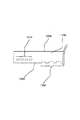
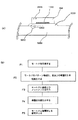
図1で、1100はモールド、1050は第1の面、1060は該第1の面と反対側に位置する第2の面であり、1000は、第1の面に形成されているパターン領域である。1070は、第1の面側と第2の面側に露出しないように埋め込まれている位置合わせのためのマークである。
モールドの構成材料と前記マーク1070とを異なる材料で作製し、両者に屈折率差をもたせる。当該マークを光学的に読みとることを考慮すると、屈折率差は、例えば0.1以上であるのがよい。マーク1070はモールドとの屈折率差が確保でき、光学的に読みとることができれば、特に材料は限定されない。空孔とすることもできる。空孔の部分は真空にしたり、空気や窒素ガスなどの気体が充填されててもよい。
本実施形態においては、アライメント用のマーク1070が、埋め込まれていることが重要であり、斯かる構成により、インプリントを行う際に、基板とモールドとの間に介在する樹脂層により、当該マークが光学的に読み取り難くなるという問題を回避できる。
このような問題は、主に、アライメントマークに樹脂の残渣が付着する場合や、モールドと樹脂層との屈折率差が十分ではない場合などに生じる。なお、パターン領域1000には、モールドの表面に凹凸パターンが形成されている。プレーンな第1の面1050に、別途、凸部を設けることでパターンを形成し、当該凸部を基板に転写することもできる。
また、前記位置合わせ用マーク1070は、前記第2の面側よりも第1の面側に近い位置に設けておく方が、パターン領域1000とマーク1070とを一つの光学システムで読みとる場合には、同時に焦点を両者に合わせやすいという点から好ましい。
Next, an embodiment of the present invention will be described.
(First embodiment)
A mold according to a first embodiment of the present invention will be described with reference to FIG.
In FIG. 1, 1100 is a mold, 1050 is a first surface, 1060 is a second surface located on the opposite side of the first surface, and 1000 is a pattern region formed on the first surface. is there.
The mold constituent material and the
In the present embodiment, it is important that the
Such a problem mainly occurs when a resin residue adheres to the alignment mark or when the difference in refractive index between the mold and the resin layer is not sufficient. In the
In the case where the
なお、図2(c)のように、モールドを構成する材料と異なる材料107でアライメントマーク1070を埋め込むこともできる。
更にまた、図1の第1の面1050と同じ面にアライメントマークを作製し、それが外部に露出しないように、当該アライメントマークを保護層で覆うこともできる。斯かる場合、保護層の材料はモールドの構成材料と同じでもよいが、モールド材料とは屈折率の異なる材料を選択することもできる。なお、アライメントマークが外部に露出していないということは、インプリントを行う際に、モールドと基板間に介在する樹脂と、当該アライメントマークとが、直接接触しないことを意味する。
モールドは、光硬化性の樹脂を使用するインプリント方法においては、光透過性の物質(例えば、石英、パイレックス(登録商標)、サファイアなど)で構成される。勿論光を用いて透過させる必要が無い場合は、させないのであれば、金属材料やSiを用いることもできる。
以下に、図1のようにアライメントマークが埋め込まれたモールドの製造方法を、図13(a)から(e)と図14を用いて後述している。
As shown in FIG. 2C, the
Furthermore, an alignment mark can be formed on the same surface as the
In the imprint method using a photocurable resin, the mold is made of a light-transmitting substance (for example, quartz, Pyrex (registered trademark), sapphire, etc.). Of course, when there is no need to transmit light, a metal material or Si can be used as long as the light is not transmitted.
Hereinafter, a method of manufacturing a mold in which alignment marks are embedded as shown in FIG. 1 will be described later with reference to FIGS. 13 (a) to 13 (e) and FIG.
基板とモールド間に樹脂を介在させて、モールドが有する凹凸パターンを転写する際に、モールドのアライメントマークへの樹脂の付着を防止するという観点からは以下の構成にすることもできる。
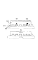
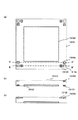
例えば、図2に示すように、モールドのパターン領域面の面内方向に関して、光学的特性が変化する位置合わせ構造を構成する。
図2において、101は加工面、102は位置合わせ構造面、103は距離A、104はモールド、105はパターン用モールド(第1の部材)、106は位置合わせ用モールド(第2の部材)、107は光透過性物質である。
図2(a)は、加工面101と位置合わせ構造面102を一定の距離A103離し、後退させた構成例である。この距離は樹脂が接触しないような位置であり、顕微鏡の焦点深度によって数μm〜数mmとすることが好ましい。
また、図2(b)は、転写用の凹凸パターンが形成された第1の部材と、位置合わせ構造102が形成された第2の部材との、2つの部材を張り合わせて形成した構成例である。このように2つの部材を張り合わせることで、位置合わせ構造を凹凸パターン面から容易に後退させた構成を得ることができる。
また、図2(c)は、位置合わせ構造を光透過物質中に埋めるようにした構成例であり、詳細は上述の通りである。また、図2(d)は、位置合わせ構造を加工面の反対の面に形成した構成例である。
From the viewpoint of preventing the resin from adhering to the alignment mark of the mold when the concave / convex pattern of the mold is transferred by interposing the resin between the substrate and the mold, the following configuration may be employed.
For example, as shown in FIG. 2, an alignment structure in which the optical characteristics change with respect to the in-plane direction of the pattern area surface of the mold is formed.
In FIG. 2, 101 is a processing surface, 102 is an alignment structure surface, 103 is a distance A, 104 is a mold, 105 is a pattern mold (first member), 106 is an alignment mold (second member),
FIG. 2A shows a configuration example in which the
FIG. 2B shows a configuration example in which two members, that is, a first member on which a concavo-convex pattern for transfer is formed and a second member on which an
FIG. 2C shows a configuration example in which the alignment structure is embedded in the light transmitting material, and the details are as described above. FIG. 2D shows a configuration example in which the alignment structure is formed on the surface opposite to the processing surface.
なお、本発明者らの検討によれば、位置あわせ構造を加工面と同一面側に形成する場合(図2(a)や(b)の場合)は、加工面から数μmから数mmの範囲で後退させることが好ましいことが分かった。
一般に、被加工基板上の樹脂は、1μmあるいはそれ以下の厚さが塗布等されるが、押圧により樹脂が盛り上がる可能性を考慮すると、加工面のレベルから数μm以上は離れていることが望ましい。また、加工面と位置あわせ構造があまりにも離れるとモールドの構造設計上の精度が悪くなる為、数mm以下が望ましい。数μmとは、例えば、2、3μmである。数mmとは、例えば2、3mmである。勿論、モールドの加工面と反対側の面やモールド構成部材の内部に位置あわせ構造がある場合は、本発明は上記数値範囲に限られるものではない。
また、位置合わせ構造は、例えば、ボックス、クロス、バーにより、あるいは周期構造によって構成することができ、また、これらの組合せによっても構成することができる。
According to the study by the present inventors, when the alignment structure is formed on the same surface side as the processing surface (in the case of FIGS. 2A and 2B), it is several μm to several mm from the processing surface. It has been found that it is preferable to reverse the range.
In general, the resin on the substrate to be processed is applied with a thickness of 1 μm or less, but considering the possibility that the resin swells by pressing, it is desirable that the resin is separated by several μm or more from the level of the processed surface. . In addition, if the processed surface and the alignment structure are too far apart, the accuracy of the mold structural design is deteriorated. The term “several μm” is, for example, 2, 3 μm. The several mm is, for example, a few mm. Of course, the present invention is not limited to the above numerical range when there is an alignment structure on the surface opposite to the processing surface of the mold or inside the mold component.
Further, the alignment structure can be constituted by, for example, a box, a cross, a bar, or a periodic structure, and can also be constituted by a combination thereof.
次に、図2に示したモールドの製造方法の例を、図12〜図15に示す。
A)図12に、図2(a)に示されるモールドの製造方法を示す。
(1)モールド基板104に、ハードマスク層1201を成膜する(図12(a))。
(2)ハードマスク層1201上にマスク層1204を形成し、1201をエッチングする(図12(b))。
1204のパターニング方法は、例えば、ステッパ、スキャナ等による光露光、電子ビームによる描画がある。図中、1202は位置合わせ構造を有する領域、1203は、実パターンを有する領域である。
(3)ハードマスク層1201をマスクに、あるいはハードマスク層1201とマスク層1204の残膜との併用で、モールド基板104を、所望の深さまでエッチングする(図12(c))。
ここで言う所望の深さとは、実パターン領域1203にて、インプリントに必要な深さのことである。この工程の後、マスク層1204が残っている場合は、アッシング等の処理により除去する。
(4)マスク層1205にて、位置合わせ構造領域1202以外のモールド表面を被覆する(図12(d))。
(5)ハードマスク層1201をマスクに、モールド基板104を、所望の深さまでエッチングする(図12(e))。
ここで言う所望の深さとは、位置合わせ構造面102と加工面101の距離A103となる深さより数10nm〜数μm深い深さのことである。
(6)1205をマスク層にしてハードマスク層1201をエッチングし、引き続き104を距離A103の深さまでエッチングする。
この時の104のエッチング表面が、位置合わせ構造102となる(図12(f))。
(7)1205を除去する(図12(g))。
(8)1201を除去する(図12(h))。ただし、1201が光透過性物質であれば、必ずしも除去する必要はない。
B)図13に、図2(b)に示されるモールドの作製方法を示す。
(1)モールド基板106に、光透過性物質1301を成膜する(図13(a))。
1301はモールド基板106とは異なる物質であり、エッチングの選択性が取れる組み合わせであることが望ましい。例えば、光透過性物質とは、例えばSiNやTiO2やAl2O3などから構成でき、モールド基板はSiO2やCaF2やITOなどから構成できる。
(2)1301上に、1301とは異なる光透過性物質105を成膜する。105は106と同じ物質であっても良い(図13(b))。
(3)ハードマスク層1201を成膜する(図13(c))。このハードマスク層は、例えば、SiN、TiO2、Al2O3等の光透過性物質、あるいはCr、WSi、Al等のメタル材、あるいはSi等から構成できる。
(4)ハードマスク層1201上にマスク層1204を形成し、1201をエッチングする(図13(d))。マスク層1204は、例えば、光リソグラフィーや電子線リソグラフィー等で用いられる一般的なレジスト材料から適宜選ばれる。
1204のパターニング方法は、例えば、ステッパ、スキャナ等による光露光、電子ビームによる描画がある。図中、1202は位置合わせ構造領域、1203は、実パターン領域である。
(5)ハードマスク層1201をマスクに、あるいはハードマスク層1201とマスク層1204の残膜との併用で、光透過性物質105を、所望の深さまでエッチングする(図13(e))。
ここで言う所望の深さとは、実パターン領域1203にて、インプリントに必要な深さのことである。この工程の後、マスク層1204が残っている場合は、アッシング等の処理により除去する。
(6)マスク層1205にて、位置合わせ構造領域1202以外のモールド表面を被覆し、ハードマスク層1201をマスクに、光透過性物質105を、光透過性物質1301の表面に至るまでエッチングする(図13(f))。マスク層1205は、上記(4)と同じように一般的なレジスト材料から選ばれる。
(7)光透過性物質105のエッチング底部に露出した1301、及び、ハードマスク層1201のエッチングを行う。これらの工程は、別々に行っても良いが、同じ工程で同時にエッチングされる場合もある。その後、1205をマスク層として、105を光透過性物質1301の表面に至るまでエッチングする(図13(g))。
(8)1205を除去する(図13(h))。
(9)露出した1301、及び1201を除去する(図13(i))。ただし、1201が光透過性物質であれば、必ずしも除去する必要はない。位置合わせ構造面102と加工面101の距離A103は、105の膜厚によって決定される。こうして、パターン領域101から後退した位置にアライメントマーク102を有するモールドが実現する。
C)図14に、図1や図2(c)に示されるアライメントマークが埋め込まれたモールドの作製方法を示す。
(1)上記B)で示したように、図13(a)〜図13(e)までの工程を実施する。
(2)図13(f)と同様にマスク層1205を用いて、光透過性物質105のエッチング底部に露出した1301のエッチングを行う(図14(a))。
(3)モールド表面全体に、例えば、SiO2、無機SOG(Spin On Glass)、有機SOGなどからなる光透過性物質107を成膜する。成膜方法は、スピンコート、CVD等が考えられる(図14(b))。上記(2)においてエッチングにより作製した凹部1212に充填されるように成膜する。
(4)光透過性物質107を、凹部1212に充填された同物質107を残すように、モールド基板の表面まで除去する(図14(c))。
モールド基板の表面とは、位置合わせ構造領域1202においてはハードマスク層1201上、その他の領域に関しては、マスク層1205のことを指すが、位置合わせ構造領域1202のハードマスク層1201が露出した時点を優先とする。除去方法としては、全面エッチバック、あるいはCMP等の方法が考えられる。
(5)マスク層1205を除去する(図14(d))。これにより、もしマスク層1205上に光透過性物質107が残っていた場合は、リフトオフされる。
(6)ハードマスク層1201を除去する(図14(e))。
ただし、1201が光透過性物質であれば、必ずしも除去する必要はない。位置合わせ構造面102と加工面101の距離A103は、105の膜厚によって決定される。
ただし、このモールドにおいては、光透過性物質1301が106、105、107の中に埋まっている構造となるため、位置合わせ構造を観測するためには、これらの物質と光学的にコントラストの取れる組み合わせであることが必要となる。
D)図15に、図2(d)に示されるモールドの製造方法を示す。
(1)モールド基板104の表面に、マスク層1501を形成する(図15(a))。
マスク層1501は、レジストでもハードマスクでも良い。また、マスク層1501は、実パターン領域1203と、表裏位置合わせ構造領域1502有する。マスク層1501のパターニング方法は、例えば、ステッパ、スキャナ等による光露光、電子ビームによる描画がある。
(2)マスク層1501を用いて、モールド基板の104を所望の深さまでエッチングする(図15(b))。
ここで言う所望の深さとは、実パターン領域1203にて、インプリントに必要な深さのことである。
(3)表面にレジスト等による保護層1503を形成した後、裏面にマスク層1504を形成する(図15(c))。
マスク層1504は、位置合わせ構造領域1202と、表裏アライメント領域1505を有する。表裏位置合わせ構造領域1502と1505を光学的にアライメントすることにより、両者の位置関係を合わせる。
(4)1504をマスク層にして、104を所望の深さまでエッチングする(図15(d))。
ここで言う所望の深さとは、位置合わせ構造が、光学的にコントラストが取れる深さであればいくらでも良い。
(5)レジスト1503、マスク層1501とマスク層1504を除去する(図15(e))。
ただし、マスク層1501とマスク層1504が光透過性物質であれば、必ずしも除去する必要はない。
位置合わせ構造面102と加工面101の距離A103は、モールド基板104の板厚によって決定される。
こうして、加工面101に形成されるパターン領域1203と同一面に第1のマーク1077を有し、このパターン領域が形成されている面とは反対側の面に、アライメント用の第2のマーク1202を有するモールドが実現される。このような2つのマークを有するモールドに関しては、以下の第2の実施形態において詳述する。
以上、モールドの作製方法について説明したが、特に、図12〜図14のプロセスには、2つの異なる面に形成するパターンの描画を一度に行えるという利点がある。段差の存在するサンプルでは、焦点深度の関係から、1回の描画で双方の面で充分な解像度を得るのは困難である。一方、2回に分けて描画した場合、アライメントによる誤差が乗るため、2つのパターン間の相対距離が設計通りにならない。図12〜図14に示す作製方法では、描画は一回で済み、かつ異なる2つの面において、同等の解像度を持ったパターンを形成することが出来る。
Next, an example of a method for manufacturing the mold shown in FIG. 2 is shown in FIGS.
A) FIG. 12 shows a method for manufacturing the mold shown in FIG.
(1) A
(2) A
Examples of the
(3) The
The desired depth referred to here is a depth necessary for imprinting in the
(4) The
(5) Using the
The desired depth referred to here is a depth that is several tens of nm to several μm deeper than the depth corresponding to the distance A103 between the
(6) The
The
(7) 1205 is removed (FIG. 12 (g)).
(8) 1201 is removed (FIG. 12H). However, if 1201 is a light-transmitting substance, it is not necessarily removed.
B) FIG. 13 shows a method for producing the mold shown in FIG.
(1) A
1301 is a material different from that of the
(2) A
(3) A
(4) A
Examples of the
(5) The
The desired depth referred to here is a depth necessary for imprinting in the
(6) The mold layer other than the
(7) Etching is performed on 1301 and the
(8) 1205 is removed (FIG. 13 (h)).
(9) The exposed 1301 and 1201 are removed (FIG. 13 (i)). However, if 1201 is a light-transmitting substance, it is not necessarily removed. The distance A103 between the
C) FIG. 14 shows a method for producing a mold in which the alignment mark shown in FIG. 1 or FIG. 2 (c) is embedded.
(1) As shown in B) above, the steps from FIG. 13A to FIG. 13E are performed.
(2)
(3) A
(4) The
The surface of the mold substrate refers to the
(5) The
(6) The
However, if 1201 is a light-transmitting substance, it is not necessarily removed. The distance A103 between the
However, this mold has a structure in which the
D) FIG. 15 shows a method for manufacturing the mold shown in FIG.
(1) A
The
(2) Using the
The desired depth referred to here is a depth necessary for imprinting in the
(3) After forming a
The
(4)
The desired depth here may be any depth as long as the alignment structure has a depth that allows optical contrast.
(5) The resist 1503, the
Note that the
A distance A103 between the
Thus, the
The method for producing a mold has been described above. In particular, the processes of FIGS. 12 to 14 have an advantage that a pattern formed on two different surfaces can be drawn at a time. In a sample having a step, it is difficult to obtain sufficient resolution on both sides in one drawing because of the depth of focus. On the other hand, when drawing is performed twice, an error due to alignment is added, so the relative distance between the two patterns is not as designed. In the manufacturing method shown in FIGS. 12 to 14, drawing is performed only once, and patterns having the same resolution can be formed on two different surfaces.
本実施の形態におけるモールドの幾つかの構成例を示したが、本発明のモールドはこれらの構成例のものに限定されるものではない。
上記したようにワークへ転写するための凹凸パターンが形成された加工面から樹脂が接触しないような領域に、面内方向に光学的特性が変化する位置合わせ構造を有するものであれば、上記以外のものも、本発明のモールドに含まれることは言うまでもない。
Although some configuration examples of the mold in the present embodiment have been shown, the mold of the present invention is not limited to these configuration examples.
As long as it has an alignment structure whose optical characteristics change in the in-plane direction in a region where the resin does not come into contact with the processed surface on which the uneven pattern for transferring to the workpiece is formed as described above, other than the above Needless to say, these are also included in the mold of the present invention.
なお、上記モールドを用いて実際に位置合わせを行う場合には、上記したモールドが有する位置合わせ構造と、ワークあるいはワークの支持台に形成された位置合わせ構造とを用いて、位置合わせが行われる。
以上による本発明に係るモールドは、各種インプリント(熱により樹脂を硬化させる熱インプリント方法など)に適用可能であるが、特に光硬化樹脂を用いるインプリンティング(光インプリント)に好適に用いることができる。
In the case of actually performing the alignment using the mold, the alignment is performed using the alignment structure of the mold and the alignment structure formed on the workpiece or the work support base. .
The mold according to the present invention as described above can be applied to various imprints (such as a thermal imprint method in which a resin is cured by heat), but is particularly suitable for imprinting (photoimprinting) using a photocurable resin. Can do.
(第2の実施形態)
つぎに、本発明の第2の実施形態に係るモールドについて説明する。
本実施形態に係るモールドは、以下のような特徴を有している。
すなわち、転写するためのパターン領域を有する第1の面と、該第1の面と反対側に位置する第2の面と、該第1の面に設けられている第1のマークと、該第1の面から該第2の面側へ後退した位置に設けられている、位置合わせのための第2のマークを有する。
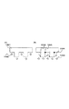
第2のマークとは、例えば、図3の102である。
具体的には、図3を用いて説明する。図3において、図2と同じ引用番号が付されているものは、図2と同じものを指している。1077は、パターン領域101と同じ面に設けられている第1のマークである。なお、101は、実際の凹凸は不図示であるが、凹凸パターン領域である。第1の面とはパターン領域101が形成されている面であり、第2の面とは、第1の面と対向する反対側の面3101である。
(Second Embodiment)
Next, a mold according to a second embodiment of the present invention will be described.
The mold according to the present embodiment has the following characteristics.
That is, a first surface having a pattern region for transfer, a second surface positioned on the opposite side of the first surface, a first mark provided on the first surface, A second mark for alignment is provided at a position retracted from the first surface to the second surface side.
The second mark is, for example, 102 in FIG.
Specifically, this will be described with reference to FIG. In FIG. 3, the same reference numerals as those in FIG. 2 are the same as those in FIG. 2.
前記第2のマークは、前記第1及び第2の面との間、あるいは前記第2の面に設けられる。図3(a)や(b)では、第1の面から後退した位置に第2のマークが設けられている。勿論、前記第2のマークは、図3(c)のように前記第1及び第2の面との間の領域に埋め込まれていてもよい。また、図3(d)のようにパターン領域が形成されている第1の面とは反対側の第2の面に、第2のマーク102を設けてもよい。
例えば、第1のマークをパターン領域面と同じ面に設け、アライメント用の第2のマークを、モールドの反対側の面に有するモールドは、図15に記載した製造方法により作製することができる。図15の説明は上述した通りである。図15(d)における1077が第1のマークである。
また、本実施形態に記載したように第1のマークをパターン領域と同一面に設け、第2のパターン領域を、モールドの反対側の面に有するモールドとしては、図20(a)から(e)に示すようなモールドがある。
The second mark is provided between the first surface and the second surface or on the second surface. 3A and 3B, a second mark is provided at a position retracted from the first surface. Of course, the second mark may be embedded in a region between the first and second surfaces as shown in FIG. Further, as shown in FIG. 3D, the
For example, a mold having the first mark provided on the same surface as the pattern region surface and the second mark for alignment on the surface opposite to the mold can be manufactured by the manufacturing method shown in FIG. The description of FIG. 15 is as described above.
Further, as described in this embodiment, a mold having the first mark provided on the same surface as the pattern region and the second pattern region on the surface opposite to the mold is shown in FIGS. There is a mold as shown in FIG.
このように2つの位置にアライメントマークがあることにより、一方のアライメントマークでの位置合わせが困難である場合も、他方のアライメントマークでの位置合わせが可能となる。
特に、前記パターン領域と同一面に第1のマーク(図3における1077)を設け、当該マークから、モールド104の厚さ方向に後退した位置に第2のマークを設けることにより次の効果が期待される。すなわち、パターン領域101(図3(c)の1000)を基準に考えると、裏面にある第2のマークの位置は、設計上での位置と作製された実際の位置とに差異が生じる場合がある。
当該差異が、インプリントプロセスを行う上で事実上問題にならなければ、そのような差異は生じても、上記第1の実施形態で説明したモールドを使用することができる。
但し、そのような差異を考慮してインプリントプロセスを行う必要がある場合は、本実施形態のモールドは極めて有用である。このような差異が生じる理由を説明する。
基板の両面側に同時に凹凸を形成できないために、パターン領域の形成とは別工程で第2のマークが形成されるためである。一方、第1のマークは、パターン領域と同一の工程で作製できるために、設計上の位置に極めて近い位置に実際に形成することができる。本実施形態に記載のモールドは、第1のマークと第2のマークとの相対的な位置関係を把握できるので、パターン領域あるいは第1のマークに対して、設計上の位置からどのような誤差で第2のマークが形成されているかの情報が分かる。
なお、モールド(テンプレートと呼ばれる場合もある。)の材料は実施形態1で説明した材料を用いることができる。
As described above, the alignment marks at the two positions enable the alignment with the other alignment mark even when the alignment with one alignment mark is difficult.
In particular, the following effect can be expected by providing a first mark (1077 in FIG. 3) on the same surface as the pattern region and providing the second mark at a position retracted from the mark in the thickness direction of the
If the difference does not cause a problem in the imprint process, the mold described in the first embodiment can be used even if such a difference occurs.
However, when it is necessary to perform the imprint process in consideration of such a difference, the mold of this embodiment is extremely useful. The reason why such a difference occurs will be described.
This is because the concave and convex portions cannot be formed on both sides of the substrate at the same time, so that the second mark is formed in a separate process from the formation of the pattern region. On the other hand, since the first mark can be manufactured in the same process as the pattern region, it can be actually formed at a position very close to the designed position. Since the mold described in the present embodiment can grasp the relative positional relationship between the first mark and the second mark, any error from the design position with respect to the pattern region or the first mark can be determined. Thus, information on whether or not the second mark is formed can be obtained.
Note that the material described in
(第3の実施形態)
つぎに、本発明の第3の実施形態に係るパターン形成方法について説明する。
本実施形態に係るパターン形成方法は、以下のように行われる。
まず、パターン領域を含む第1の面と、該第1の面の反対側に位置する第2の面と、該第1の面から該第2の面側へ後退した位置に設けられているアライメントマークとを備えているモールドを用意する。例えば、図1や図2や図3に記載の如きモールドである。
そして、該モールドが有する該パターン領域と、基板上の被覆材(例えば、光硬化性の樹脂やレジストである。)とを接触させる。
(Third embodiment)
Next, a pattern forming method according to the third embodiment of the present invention will be described.
The pattern forming method according to the present embodiment is performed as follows.
First, a first surface including a pattern region, a second surface located on the opposite side of the first surface, and a position retracted from the first surface to the second surface side are provided. A mold having an alignment mark is prepared. For example, a mold as shown in FIG. 1, FIG. 2, or FIG.
And the pattern area | region which this mold has, and the coating | covering material (For example, it is a photocurable resin and a resist) are made to contact.
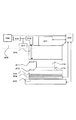
図17(a)において、5000は基板、3000は被覆材、104はモールドである。1000は被覆材に転写するべき凹凸パターンが形成されている領域である(実際の凹凸は不図示である。)。2070は上記アライメントマークである。後退した位置として、モールド104の裏面側にアライメントマークを設けた構成を示している。勿論、本実施形態においては、アライメントマークの位置は、モールドの裏面に限られるものではない。
そして、被覆材3000を基板全面に塗布したり、あるいはモールドのパターン領域以上のエリアに塗布する。これにより、該アライメントマーク2070と該基板5000とが対向している該基板上の箇所5050(同図の点線枠)に、該被覆材3000が配置された状態になる。
この状態で、該モールドと該基板の位置に関する情報(例えば、画像情報)を、該アライメントマークと該基板側のマーク5300とを用いて取得する。
そして、前記情報に基づいて、該パターン領域の面内方向に関する、該基板と該モールドとの位置合わせを行う。具体的には、モールド側から、アライメントマーク2070と5300とを一つの撮像素子で光学的に読みとり、面内方向の位置合わせを行う。本実施形態におけるパターン形成方法においては、当該位置合わせを、該パターン領域と該被覆材とが接触している状態(接触状態)で行うことができる。勿論、面内方向に関するモールドと基板との位置合わせを常に前記接触状態で行うことは必須ではなく、本実施形態に係る発明には、非接触状態でモールドと基板との位置合わせを行うことも包含される。
In FIG. 17A, 5000 is a substrate, 3000 is a coating material, and 104 is a mold.
Then, the
In this state, information about the positions of the mold and the substrate (for example, image information) is acquired using the alignment mark and the
Based on the information, the substrate and the mold are aligned with respect to the in-plane direction of the pattern region. Specifically, the alignment marks 2070 and 5300 are optically read by one image sensor from the mold side, and alignment in the in-plane direction is performed. In the pattern forming method in the present embodiment, the alignment can be performed in a state where the pattern region and the covering material are in contact (contact state). Of course, it is not always necessary to align the mold and the substrate in the in-plane direction in the contact state. In the invention according to the present embodiment, the mold and the substrate can be aligned in a non-contact state. Is included.
モールドの屈折率と被覆材の屈折率差が小さい場合、パターン領域1000側にモールドのアライメントマークがあれば、被覆材とモールドとの接触により当該マークは光学的に読みとり難くなったり、あるいは読みとれなくなる。本実施形態で示したパターン形成方法によれば、アライメントマーク2070と被覆材3000(例えば、樹脂やレジストであり、紫外線等の光硬化性を有する材料である。)とが接触することが無い。したがって、モールドと基板間に介在させる被覆材の被覆領域を厳密に制御する必要が無くなる。スピン塗布を用いて被覆材を設けることも可能となる。勿論、ディスペンサーを用いて基板上に多数のドット状の被覆材を設けて、モールドと基板間の距離を縮めることで、被覆材がパターン領域全面に連続膜として介在するようにしてもよい。
When the refractive index difference between the mold and the coating material is small, if there is a mold alignment mark on the
被覆材とは、例えば光硬化性の樹脂であるが、前記位置合わせを行いながら、前記被覆材を硬化させるのがよい。モールドと基板とが樹脂を介して間接的に接触した状態で位置ズレを生じる場合があるからである。即ち、面内方向の位置制御を行いながら、基板とモールドのギャップも制御し、そのような状態で被覆材を硬化させるのがよい。被覆材の硬化は、例えば紫外線をモールド側から被覆材に照射することにより行われる。光硬化性樹脂の例としては、ウレタン系やエポキシ系やアクリル系などがある。
勿論、フェノール樹脂やエポキシ樹脂やシリコーンやポリイミドなどの熱硬化性樹脂や、ポリメタクリル酸メチル(PMMA)、ポリカーボネ−ト(PC)、PET、アクリルなどの熱可塑性樹脂を用いることもできる。必要に応じて加熱処理を行うパターンを形成する。
さらに、被覆材には、PDMS(Polydimethylsiloxane)を利用することもできる。
The covering material is, for example, a photocurable resin, but it is preferable to cure the covering material while performing the alignment. This is because misalignment may occur in a state where the mold and the substrate are indirectly in contact with each other through the resin. That is, while controlling the position in the in-plane direction, the gap between the substrate and the mold is also controlled, and the covering material is preferably cured in such a state. Curing of the coating material is performed, for example, by irradiating the coating material with ultraviolet rays from the mold side. Examples of the photocurable resin include urethane, epoxy, and acrylic.
Needless to say, thermosetting resins such as phenol resin, epoxy resin, silicone and polyimide, and thermoplastic resins such as polymethyl methacrylate (PMMA), polycarbonate (PC), PET, and acrylic can also be used. A pattern for heat treatment is formed as necessary.
Furthermore, PDMS (Polydimethylsiloxane) can be used as the covering material.
また、本実施形態においては、更に以下の制御を行うことも好ましい。
すなわち、取得された前記情報に基づいて、前記基板と前記モールド間の間隔制御を行うのである。
モールドと基板間に樹脂を介在させて、当該樹脂に圧力を加える場合、モールドと基板とが、面内方向の位置ズレを起こす場合がある。
特に、予め定められた値以上に面内方向の位置ズレが生じた場合には、モールドと基板との間隔を維持して、当該位置ズレを補正しようとすると、モールドが有するパターン領域に物理的ダメージが加わることが懸念される。したがって、そのような場合には、一旦、モールドと基板との間隔を長くする間隔制御を行う。好ましくは、一旦、モールドと基板とが樹脂を介して間接的に接触した状態を解消する位置まで、モールドを後退させる。そして、両者の位置合わせを行う。
このように、モールドが有するパターンの転写に際し、モールドおよびワーク(被加工部材)にモールドの加工面(パターン領域が形成されている第1の面)と平行な方向に力が加わり、モールドとワークの位置がずれることがある。従って、好ましくは、加圧しながら上記加工面と平行な面内方向の位置合わせをすることが好ましいのである。
In the present embodiment, it is also preferable to perform the following control.
That is, the distance between the substrate and the mold is controlled based on the acquired information.
When a resin is interposed between the mold and the substrate and pressure is applied to the resin, the mold and the substrate may be displaced in the in-plane direction.
In particular, when a positional deviation in the in-plane direction exceeds a predetermined value, if an attempt is made to correct the positional deviation while maintaining the distance between the mold and the substrate, the pattern area of the mold is physically changed. There is concern about the damage. Therefore, in such a case, the interval control for increasing the interval between the mold and the substrate is once performed. Preferably, the mold is once retracted to a position where the state where the mold and the substrate are indirectly contacted via the resin is eliminated. And both are aligned.
As described above, when transferring the pattern of the mold, a force is applied to the mold and the work (member to be processed) in a direction parallel to the processing surface of the mold (the first surface on which the pattern region is formed). May be misaligned. Therefore, it is preferable to align in the in-plane direction parallel to the processed surface while applying pressure.
なお、基板の材料としては、Si基板、GaAs基板等の半導体基板、あるいはこれらの半導体基板に樹脂をコートしたもの、あるいは樹脂板、ガラス基板、等を用いることもできる。更に、これらの材料からなる基板に、薄膜を成長させたり、貼り合わせたりして形成される多層基板も使用できる。勿論、石英基板などの光透過性の基板を使用することもできる。基板の材料に関しては、以降の実施形態においても同様である。
また、基板側のアライメントマークは、基板自体に、あるいは基板に積層されている膜に直接設けてもよいし、基板を支持する支持部材や台座に設けることもできる。なお、本発明において、アライメントマークを有する基板とは、基板自体に設けられている場合と、基板上に積層された膜にアライメントマークが設けられている場合との両方を含む。
As the substrate material, a semiconductor substrate such as a Si substrate or a GaAs substrate, a resin substrate coated with a resin, a resin plate, a glass substrate, or the like can be used. Furthermore, a multilayer substrate formed by growing or bonding a thin film on a substrate made of these materials can also be used. Of course, a light-transmitting substrate such as a quartz substrate can also be used. The same applies to the material of the substrate in the following embodiments.
The alignment mark on the substrate side may be provided directly on the substrate itself or on a film stacked on the substrate, or may be provided on a support member or a pedestal that supports the substrate. In the present invention, the substrate having an alignment mark includes both the case where the alignment mark is provided on the substrate itself and the case where the alignment mark is provided on a film laminated on the substrate.
本実施形態で説明したパターン形成方法の一例を図17(b)に示している。まず、パターン領域から後退した位置にアライメントマークを有するモールドを用意するプロセスである(P1)。
パターン領域と基板上に設けられている被覆材(例えば、光硬化性の樹脂)とを接触させる(P2)。勿論、接触させる際には、モールドと基板との位置合わせを行った後に接触させるのがよい。なお、モールドのパターン領域には、予め離型材として、フッ素系シランカップリング材などを塗布しておき、被覆材が硬化した後にモールドと基板とを離れやすくする場合がある。従って、本発明において、パターン領域(あるいはモールド)と被覆材とが接触するとは、直接的に両者が接触する場合は勿論、離型材など別な層を介して、両者が接触する場合の両方を意味する。他の実施形態や実施例においても同様である。
次に、モールドのパターン領域と被覆材とが接触した状態で、モールドと基板とのアライメントを行う(P3)。このアライメントの際には、モールドに設けられている面内方向のアライメントマークと、基板側のアライメントマークとが対向しているエリア(図17(a)の5300)にも、前記被覆材が存在する。勿論、前記エリアには被覆材が存在しないように行うこともできるが、基板上への被覆材の厳密な塗布量制御が緩和できること、スピン塗布法を利用できることからも、前記エリアに被覆材が存在してもアライメントを行えるのがよい。アライメントは以下のように行う。
具体的には、モールドのパターン領域が基板上の所望の位置にあるように、パターン領域が形成されている面の面内方向に関して、モールドと基板とのアライメントを行う。モールドと基板とを、相対的に面内方向に移動させることでアライメントを行う。
An example of the pattern forming method described in this embodiment is shown in FIG. First, a process of preparing a mold having an alignment mark at a position retracted from the pattern region (P1).
The pattern region is brought into contact with a covering material (for example, photocurable resin) provided on the substrate (P2). Of course, when contacting, it is good to contact after aligning a mold and a board | substrate. In some cases, a fluorine-based silane coupling material or the like is previously applied as a mold release material to the pattern area of the mold so that the mold and the substrate can be easily separated after the coating material is cured. Therefore, in the present invention, the pattern region (or mold) and the covering material are in contact with each other not only when they are in direct contact but also when they are in contact via another layer such as a release material. means. The same applies to other embodiments and examples.
Next, the mold and the substrate are aligned in a state where the pattern area of the mold and the covering material are in contact with each other (P3). During this alignment, the covering material is also present in the area (5300 in FIG. 17A) where the alignment mark in the in-plane direction provided on the mold and the alignment mark on the substrate side face each other. To do. Of course, it is possible to perform the coating so that no coating material is present in the area. Even if it exists, it should be possible to perform alignment. Alignment is performed as follows.
Specifically, the mold and the substrate are aligned in the in-plane direction of the surface on which the pattern region is formed so that the pattern region of the mold is at a desired position on the substrate. Alignment is performed by relatively moving the mold and the substrate in the in-plane direction.
その際に、基板に設けられているマークと、本実施形態で説明したように、モールドに設けられているアライメントマーク(2070)とを用いて、両者の位置調整を行う。なお、モールドと基板とのギャップが所望の値になるように、両者を相対的に近づける、このギャップ調整は必要に応じて行えばよい。ギャップ調整する際に、面内方向の位置制御をしてもよいし、一旦所望のギャップ長になるように両者間のギャップを調整した後、面内方向の位置を調整してもよい。勿論、ギャップ調整と面内方向の位置調整とを交互に繰り返して、モールドと基板との面内方向の位置、及びギャップ長を、所望の状態にしてもよい。なお、モールドと基板とのギャップの計測は、例えば、キャパシタンスセンサ、が白色分光法エリプソメトリーを利用することができる。 At that time, the position adjustment of both is performed using the mark provided on the substrate and the alignment mark (2070) provided on the mold as described in the present embodiment. In addition, what is necessary is just to perform this gap adjustment which brings both relatively close so that the gap of a mold and a board | substrate may become a desired value. When adjusting the gap, the position in the in-plane direction may be controlled, or after adjusting the gap between the two so that the desired gap length is once obtained, the position in the in-plane direction may be adjusted. Needless to say, the gap adjustment and the position adjustment in the in-plane direction may be alternately repeated to set the position in the in-plane direction between the mold and the substrate and the gap length in a desired state. For measurement of the gap between the mold and the substrate, for example, a capacitance sensor can use white spectroscopy ellipsometry.
そして、被覆材を硬化させる(P4)。硬化させるためには、熱や、紫外線などの光を利用する。熱と光の両方を利用して被覆材を硬化させてもよい。
その後、モールドと基板を離間させる(P5)。その結果、硬化した被覆材にモールドが有していたパターンが転写される。その後、硬化した被覆材に設けられている凹凸パターンをマスクとして用いて、基板あるいは基板上の膜をエッチングする。硬化した被覆材の凹部を除去して、硬化した被覆材直下の基板を露出させた後、エッチングするのがよい。
Then, the coating material is cured (P4). In order to cure, heat or light such as ultraviolet rays is used. The coating material may be cured using both heat and light.
Thereafter, the mold and the substrate are separated (P5). As a result, the pattern that the mold had is transferred to the cured covering material. Thereafter, the substrate or the film on the substrate is etched using the concavo-convex pattern provided on the cured covering material as a mask. Etching is preferably performed after removing the concave portion of the cured coating material to expose the substrate directly under the cured coating material.
(第4の実施形態)
つぎに、本発明の第4の実施形態に係るパターン形成方法について説明する。
本実施形態におけるパターン形成方法においては、上記第2の実施形態で示したモールドを使用する。具体的には、図18(a)に示す。
モールド104のパターン領域1000が形成されている第1の面1050から後退した位置に設けられている第2のマーク2070と、基板5000側に設けられているアライメントマーク5300(第3のマーク)とを用いて、位置合わせを行う。同図において、1060は、第1の面1050から後退した位置の一例であるモールドの裏面(第2の面)である。
基板5000と基板上の被覆材3000とを合わせて、被加工物ということができるが、被覆材を介在させないで、基板自体に直接パターン形成を行うことも本実施形態には含まれる。
(Fourth embodiment)
Next, a pattern forming method according to the fourth embodiment of the present invention will be described.
In the pattern forming method in this embodiment, the mold shown in the second embodiment is used. Specifically, it is shown in FIG.
A
The
本実施形態においては、位置合わせは、具体的には、モールド側から第2のマーク2070と第3のマーク5050とを光学的に撮像素子等で読取り、それらのマークが所定の位置関係になるように、モールドと基板とを面内方向に相対的に移動させて行う。
モールド側を動かしても、基板側を動かしても両方動かしてもよい。
なお同図において、2077は、第1の面と同一面に形成されている第1のマークである。
本実施形態においては、この第1のマーク2077と第2のマーク2070との位置関係に関する情報を予め取得しておき、そして、該情報を用いて、前記モールドと前記被加工物との位置合わせを行うのがよい。
なぜなら、パターン領域1000が形成されている面と反対側の面にある第2のマークと、当該パターン領域との位置関係を、設計した通りに、ナノメートルスケールで作製するのが通常は難しいからである。
すなわち、パターン領域から面内方向にSだけ離れた位置に第2のマークを作製するように設計しても、実際には誤差αを含んだS+αの位置に作製されてしまう場合が多いのである。
一方で、パターン領域と同一面側に形成される第1のマーク2077と、当該パターン領域との位置関係は、ナノメータスケールで、設計位置とほぼ同じ位置に実際にマークを形成することができる。
例えば、パターン領域を電子線描画方式により作成する工程において、一緒にマーク部分も同方式で形成すると、設計上の位置との誤差が少ない位置に実際にマークを形成できる。
本実施形態のように、モールドの2つの面にアライメントメークを設けておくことで、パターン領域1000と第2のマークとの位置関係を保証することができるのである。
In the present embodiment, specifically, the alignment is performed by optically reading the
The mold side, the substrate side, or both may be moved.
In the figure,
In the present embodiment, information regarding the positional relationship between the
This is because it is usually difficult to produce the positional relationship between the second mark on the surface opposite to the surface on which the
That is, even if the second mark is designed to be produced at a position separated by S in the in-plane direction from the pattern region, in practice, it is often produced at the position of S + α including the error α. .
On the other hand, the
For example, in the process of creating the pattern area by the electron beam drawing method, if the mark portion is also formed by the same method, the mark can be actually formed at a position with little error from the design position.
As in this embodiment, by providing an alignment make on the two surfaces of the mold, the positional relationship between the
第1のマーク2077は実質的に設計した位置に設けられていることになる(勿論、数nmの誤差は生じる場合がある)。
したがって、この第1のマーク2077と第2のマーク2070との位置関係(例えば面内方向の位置)に関する情報を把握しておけば、パターン領域からSだけ離れた位置に作製するように設計された第2のマークの実際の位置が分かる。つまり、第2のマーク2070と第3のマーク5300を利用して精度の高いアライメントが行えるのである。換言すれば、第1のマークが見えなくなっても、第1のマークとの位置関係が分かっている、第2のマークを用いて、モールドと被加工物とのアライメントができるということである。
勿論、第1のマークと第2のマークとの位置関係は、両者の関係を直接把握しておいてもよいが、別のマークXを基準に第1のマークと第2のマークとの位置関係を間接的に把握しておき、その情報を利用することもできる。
この場合、マークXの位置は、第1及び第2のマークのうち、いずれかのマークと同一面にある方が好ましい。
The
Therefore, if the information about the positional relationship (for example, the position in the in-plane direction) between the
Of course, the positional relationship between the first mark and the second mark may be directly grasped, but the position between the first mark and the second mark with reference to another mark X. It is also possible to grasp the relationship indirectly and use the information.
In this case, it is preferable that the position of the mark X is on the same plane as one of the first and second marks.
また、本実施形態に係るパターン形成方法は、以下の特徴を有する。即ち、該モールドのパターン領域面側に設けられた第1のマークと、該パターン領域面側から後退した位置にある第2のマークとの相対的な位置関係に関する第1の位置情報と、
前記パターン領域が形成されている面から後退した位置にある第2のマークと、前記被加工物側に設けられている第3のマークとの相対的な位置関係に関する第2の位置情報とを用いて、
該パターン領域面の面内方向に関する該モールドと該被加工物(あるいは基板)との位置合わせを行うという特徴である。
The pattern forming method according to the present embodiment has the following features. That is, the first position information regarding the relative positional relationship between the first mark provided on the pattern region surface side of the mold and the second mark at a position retracted from the pattern region surface side,
Second position information relating to a relative positional relationship between a second mark at a position retracted from the surface on which the pattern region is formed and a third mark provided on the workpiece side; make use of,
This is characterized in that the mold and the workpiece (or substrate) are aligned with respect to the in-plane direction of the pattern region surface.
上記構成によれば、モールドとワークの位置を正確に検出して位置合わせをすることが可能となる。
それは、本発明者らが鋭意研究した結果、上記した従来例とは異なり、加圧しながらモールドとワークの位置合わせをした結果、光硬化樹脂がマークに接触した場合であっても、それらに影響されることなく、正確に位置の検出ができるようにしたことによる。
すなわち、上記構成によれば、加工面に設けられたマークと加工面から後退した位置に設けられたマークとの相対位置と、加工面から後退した位置に設けられたマークと被加工部材に設けられたマークとの相対位置を比較することで、位置合わせが可能となる。
このような構成によれば、モールドに設けられた加工面のマークが光硬化樹脂に接触し、信号コントラストが低くなった状態においても、モールドと基板の位置を合わせることが可能となる。
According to the said structure, it becomes possible to detect the position of a mold and a workpiece | work correctly, and to align.
As a result of diligent research by the present inventors, unlike the conventional example described above, even when the photo-curing resin is in contact with the mark as a result of aligning the mold and the workpiece while applying pressure, it affects them. This is because the position can be accurately detected without being performed.
That is, according to the above configuration, the relative position between the mark provided on the processing surface and the mark provided at the position retracted from the processing surface, and the mark provided at the position retracted from the processing surface and the workpiece are provided. By comparing the relative position with the marked mark, alignment is possible.
According to such a configuration, it is possible to align the mold and the substrate even when the mark on the processed surface provided in the mold is in contact with the photo-curing resin and the signal contrast is low.
これらを、以下に、さらに具体的に説明する。
まず、モールドの表面と表面より部材を介して後退した面にあるマークをモールドの加工面に平行な平面に投影した時の位置関係を撮像素子などによって予め計測する。
これは、既述のように同一平面内にマークを含むパターンを所望の誤差以内で作ることは容易であるのに対し、モールドの表面のマークと表面より後退した位置にあるマークの位置関係を所望の誤差以内に作ることが難しいために必要な計測である。勿論、両者の位置関係が予め分かっている場合には、この計測は省略できる。
つぎに、モールドの表面より後退した位置にあるマークと基板のマークの位置関係を撮像素子などによって計測する。
これら両方の計測値を比較することによりモールドと基板の位置を正確に検出することができる。
このような計測方法によれば、加工面のマークが光硬化樹脂に接触した状態においても、モールドのパターンを高い精度で基板に転写することが可能となる。
以上の技術は、半導体製造技術、フォトニッククリスタル等の光学素子やμ−TAS等のバイオチップの製造技術等として利用することができる。
本発明の第1の骨子は、モールドに関しては、以下の特徴を有する。即ち、モールドのパターン形成面側に設けられている第1のマークと、パターン形成面の水平位置より後退している位置(モールド内部や裏面側)に設けられている第2のマークを有する。当該2つのマークの相対位置関係が分かれば、当該マークの位置は制限されない。モールド裏面側から表面であるパターン形成面を見た場合(即ち、モールドのパターン形成面に対して鉛直方向からみた場合)、両パターンは重なっていてもよい。但し、重なっていなくてもよい。
なお、第1のマークは、モールドの加工面側にあれば特に限定されないが、モールドのパターン形成面(加工面)の水平位置と同じ水平位置に設けておく方が、作製の面からは好ましい。
被加工物側に設けられていれば、第3のマークは、被加工物を構成する基板自体に設けられていても、当該基板を支持する支持部材側に設けられていてもよい。そして、位置調整に際しては、第2のマークと第3のマークを利用して両者の位置ズレを計測すると共に、そのズレを前記第1のマークと第2のマークとの相対位置を考慮して、制御性高く、モールド表面と被加工基板との位置合わせを行うものである。
These will be described more specifically below.
First, the positional relationship when a mark on the surface of the mold and a surface receding from the surface via a member is projected onto a plane parallel to the processed surface of the mold is measured in advance by an image sensor or the like.
As described above, while it is easy to create a pattern including marks in the same plane within a desired error, the positional relationship between the mark on the surface of the mold and the mark at a position retreated from the surface is obtained. This is a necessary measurement because it is difficult to make it within the desired error. Of course, when the positional relationship between the two is known in advance, this measurement can be omitted.
Next, the positional relationship between the mark at the position retreated from the surface of the mold and the mark on the substrate is measured by an image sensor or the like.
By comparing these two measurement values, the positions of the mold and the substrate can be accurately detected.
According to such a measuring method, it is possible to transfer the pattern of the mold to the substrate with high accuracy even when the mark on the processed surface is in contact with the photo-curing resin.
The above technique can be used as a semiconductor manufacturing technique, a manufacturing technique of an optical element such as a photonic crystal, or a biochip such as μ-TAS.
The first outline of the present invention has the following characteristics regarding the mold. That is, it has the 1st mark provided in the pattern formation surface side of a mold, and the 2nd mark provided in the position (the inside of a mold, or a back surface side) receded from the horizontal position of a pattern formation surface. If the relative positional relationship between the two marks is known, the position of the mark is not limited. When the pattern forming surface which is the surface is viewed from the back side of the mold (that is, when viewed from the vertical direction with respect to the pattern forming surface of the mold), both patterns may overlap. However, they do not have to overlap.
The first mark is not particularly limited as long as it is on the processed surface side of the mold, but it is preferable from the viewpoint of production that the first mark is provided at the same horizontal position as the horizontal position of the pattern forming surface (processed surface) of the mold. .
As long as it is provided on the workpiece side, the third mark may be provided on the substrate itself constituting the workpiece or on the support member side that supports the substrate. When the position is adjusted, the positional deviation between the second mark and the third mark is measured using the second mark and the third mark, and the deviation is considered in consideration of the relative position between the first mark and the second mark. Highly controllable and aligns the mold surface with the substrate to be processed.
以下、具体的に実施例を用いて説明する。
ここで、前記位置合わせは、
前記第2のマークを基準として、前記第1のマークの水平および回転誤差である第1の誤差情報を記憶する工程と、
前記第2のマークを基準として、前記第3のマークの水平および回転誤差である第2の誤差情報を記憶する工程と、
該第1の誤差情報と該第2の誤差情報とが一致するように、前記モールドに対して、相対的に前記基板を水平移動および回転移動する工程と、を含むことが好ましい。
Hereinafter, specific examples will be described.
Here, the alignment is
Storing first error information which is a horizontal and rotational error of the first mark with respect to the second mark;
Storing second error information which is a horizontal and rotational error of the third mark with reference to the second mark;
Preferably, the method includes a step of horizontally moving and rotating the substrate relative to the mold so that the first error information matches the second error information.
また、前記位置合わせは、
前記第2のマークと前記第1のマークとの間の水平誤差あるいは回転誤差の少なくとも一方についての第1の誤差情報を記憶し、
前記第2のマークと前記第3のマークとの間の水平誤差あるいは回転誤差の少なくとも一方についての第2の誤差情報を記憶し、
該第1の誤差情報と該第2の誤差情報とを用いて、前記モールドに対して、相対的に前記被加工物を水平移動あるいは回転移動の少なくとも一方の動作を行わせること、を含むのがよい。
In addition, the alignment is
Storing first error information about at least one of a horizontal error or a rotation error between the second mark and the first mark;
Storing second error information about at least one of a horizontal error or a rotation error between the second mark and the third mark;
Using the first error information and the second error information to cause the mold to relatively move or rotate the workpiece relative to the mold. Is good.
本実施形態はもとより、既述の、あるいは後述する本発明において、被加工物(あるいは基板)と、モールド(あるいはモールドが有するパターン領域)との、面内方向の位置あわせには、以下の第1から第3の場合が少なくとも包含される。
つまり、モールドが有するパターン領域と被加工物とが平行であることを前提として、
(1)両者を相対的に水平移動あるいは回転移動させて位置合わせを行う第1の場合と、
(2)両者を相対的に水平移動及び回転移動させて、位置合わせを行う第2の場合である。ここでいう回転移動とは、例えば、基板平面に垂直な軸を中心に、モールドのパターン面を相対的に回転させることである。
(3)更に、第3の場合としては、被加工物とモールドとが非平行である場合に、両者が平行に近づくような相対的な回転動作を含む場合である。回転動作には、基板平面に垂直な軸に対して、モールドのパターン形成面の法線がなす角を変化させることが含まれる。
In addition to this embodiment, in the present invention described above or later, in the in-plane alignment of the workpiece (or substrate) and the mold (or the pattern area possessed by the mold), the following At least the first to third cases are included.
In other words, assuming that the pattern area of the mold and the workpiece are parallel,
(1) a first case in which the two are relatively horizontally moved or rotationally moved for alignment;
(2) This is a second case where the both are relatively horizontally moved and rotated to perform alignment. The rotational movement here is, for example, to relatively rotate the pattern surface of the mold around an axis perpendicular to the substrate plane.
(3) Further, as a third case, when the work piece and the mold are non-parallel, a relative rotation operation is included such that both approach parallel. The rotational operation includes changing the angle formed by the normal line of the pattern forming surface of the mold with respect to an axis perpendicular to the substrate plane.
本実施形態で説明したパターン形成方法の一例を図18(b)に示す。
まず、上述した第1及び第2のマークを有するモールドを用意する(P11)。次に、パターン領域と基板上の被覆材とを接触させる(P22)。
この例では、被覆材を有する基板が、被加工物に該当する。
そして、第2のマークと、基板側の第3のマークとを光学的に読み取ることで、モールドと基板との位置合わせを行う。
その際、モールドが有する第1のマークと第2のマークとの位置関係に関する情報を用いて、位置合わせをする。
当該情報は、第1のマークと第2のマークの両方を撮像素子で、読み取ることで得られる。これにより、第2のマーク位置が保証されていない場合も、第2のマークと基板側の第3のマークを用いた精度の高い位置合わせが可能となる。
実際に行うべき位置合わせは、パターン領域を基板上の所望の位置にあわせることなので、結果として光学的に観測される第2のマークと第3のマークとが重なり合わない位置関係になるようにアライメントすることが求められる場合もある。
モールドと基板との位置合わせができた後は、被覆材を硬化させる(P44)。その後、モールドと基板とを離間させる(P55)。こうして、パターン形成が実現される。
なお、P11、P22、P44、P55の工程は、第3の実施形態において図17(b)を用いて説明した箇所(P1、P2、P4、P5)をそのまま適用できるので詳細は省略する。
また、P44の工程は、被加工物が、基板自体である場合は、当該工程は省略されて、基板とモールド間に圧力をかけることによりパターンを形成することになる。
その際、基板に熱を加えて、軟化させることを利用してもよい。また、被加工物が、基板自体である場合は、P55の工程は、モールドと基板とを離間させるということになる。
An example of the pattern forming method described in the present embodiment is shown in FIG.
First, a mold having the above-described first and second marks is prepared (P11). Next, the pattern region and the covering material on the substrate are brought into contact (P22).
In this example, a substrate having a coating material corresponds to a workpiece.
Then, the mold and the substrate are aligned by optically reading the second mark and the third mark on the substrate side.
At that time, alignment is performed using information on the positional relationship between the first mark and the second mark of the mold.
The information can be obtained by reading both the first mark and the second mark with an image sensor. Thereby, even when the second mark position is not guaranteed, highly accurate alignment using the second mark and the third mark on the substrate side becomes possible.
Since the alignment to be actually performed is to align the pattern region with a desired position on the substrate, as a result, the second mark and the third mark that are optically observed do not overlap each other. In some cases, alignment is required.
After the alignment between the mold and the substrate is completed, the coating material is cured (P44). Thereafter, the mold and the substrate are separated (P55). In this way, pattern formation is realized.
Note that the steps P11, P22, P44, and P55 can be applied to the portions (P1, P2, P4, and P5) described in the third embodiment with reference to FIG.
In the process of P44, when the workpiece is the substrate itself, the process is omitted, and a pattern is formed by applying pressure between the substrate and the mold.
At that time, heat may be applied to the substrate to soften it. Further, when the workpiece is the substrate itself, the process of P55 means that the mold and the substrate are separated from each other.
次に、P33について詳述する。
P33におけるアライメントの際には、モールドに設けられている第2のマークと、基板側の第3のマークとが対向しているエリア(図17(a)の5300)にも、前記被覆材が存在していてもよいし、存在しないように、被覆材を基板上に設けてもよい。
アライメントは、モールドのパターン領域が基板上の所望の位置にあるように、パターン領域が形成されている面の面内方向に関して、モールドと基板とのアライメントを行う。モールドと基板とを、相対的に面内方向に移動させることでアライメントを行う。
その際に、基板に設けられている第3のマークと、本実施形態で説明したように、モールドに設けられている第2のマーク(2070)とを用いて、両者の位置調整を行う。
その際、第2のマークの位置が、設計した位置とはズレている場合があるので、第1のマークと第2のマークとの位置関係を考慮した位置合わせを行う。
なお、モールドと基板とのギャップが所望の値になるように、両者を相対的に近づける、このギャップ調整は必要に応じて行えばよい。
ギャップ調整する際に、面内方向の位置制御をしてもよいし、一旦、所望のギャップ長になるように両者間のギャップを調整した後、面内方向の位置を調整してもよい。
勿論、ギャップ調整と面内方向の位置調整とを交互に繰り返して、モールドと基板との面内方向の位置、及びギャップ長を、所望の状態にしてもよい。
Next, P33 will be described in detail.
In the alignment in P33, the covering material is also applied to the area (5300 in FIG. 17A) where the second mark provided on the mold and the third mark on the substrate side face each other. It may be present or a coating material may be provided on the substrate so that it does not exist.
In the alignment, the mold and the substrate are aligned in the in-plane direction of the surface on which the pattern region is formed so that the pattern region of the mold is at a desired position on the substrate. Alignment is performed by relatively moving the mold and the substrate in the in-plane direction.
At that time, using the third mark provided on the substrate and the second mark (2070) provided on the mold as described in the present embodiment, the position of both is adjusted.
At this time, since the position of the second mark may deviate from the designed position, alignment is performed in consideration of the positional relationship between the first mark and the second mark.
In addition, what is necessary is just to perform this gap adjustment which brings both relatively close so that the gap of a mold and a board | substrate may become a desired value.
When adjusting the gap, the position in the in-plane direction may be controlled, or the position in the in-plane direction may be adjusted once the gap between the two is adjusted so as to have a desired gap length.
Of course, the gap adjustment and the position adjustment in the in-plane direction may be alternately repeated so that the position of the mold and the substrate in the in-plane direction and the gap length are in a desired state.
なお、モールドのパターン領域面側にある第1のマークと、モールドの厚さ方向に後退した第2のマークとを用いて、2段階のアライメントを行うこともできる。例えば、モールドと基板(あるいは被加工物)とが十分に離れた状態では、第1のマークを用いて第1段階の位置合わせを行う。
その後、モールドと基板とを徐々に近づけていき、例えば、第1のマークが見え難くなったら、第2のマークを用いて第2の段階の位置合わせを行うのである。
Note that two-step alignment can be performed using the first mark on the pattern region surface side of the mold and the second mark receding in the thickness direction of the mold. For example, in a state where the mold and the substrate (or the workpiece) are sufficiently separated from each other, the first stage alignment is performed using the first mark.
Thereafter, the mold and the substrate are gradually brought closer to each other. For example, when the first mark becomes difficult to see, the second stage alignment is performed using the second mark.
(第5の実施形態)
つぎに、本発明の第5の実施形態に係るパターン形成装置について説明する。
本実施形態に係るパターン形成装置は、上記実施形態3および4に記載したパターン形成を行うために、モールド保持部と基板支持部(あるいは被加工物支持部)とを備えている。
そして、該モールド保持部と該基板支持部とが面内方向に相対的に移動するように構成されていることを特徴とする。
更に、前記モールドが有する前記パターン領域と前記被覆材とを接触させた状態で、両者の位置ずれを検出する位置ずれ検出機構と、
該検出機構からの検出情報に基づいて、前記基板と前記モールドとの間隔を制御するため間隔制御機構とを有することが好ましい。
(Fifth embodiment)
Next, a pattern forming apparatus according to a fifth embodiment of the present invention will be described.
The pattern forming apparatus according to the present embodiment includes a mold holding part and a substrate support part (or workpiece support part) in order to perform the pattern formation described in the third and fourth embodiments.
The mold holding part and the substrate support part are configured to move relatively in the in-plane direction.
Furthermore, in a state where the pattern region of the mold and the covering material are in contact with each other, a positional deviation detection mechanism for detecting a positional deviation between the two,
It is preferable to have an interval control mechanism for controlling the interval between the substrate and the mold based on detection information from the detection mechanism.
つぎに、本発明のモールドを備えたパターン形成装置について説明する。
図4において、201は光源、202は光計測システム、203はインプリント制御システム、204はワーク加圧機構、205は面内移動機構、206はモールド加圧機構である。
また、207は光源、208は解析システム、209は撮像素子、210は顕微鏡である。
また、211はモールド側の位置合わせ構造、212はワーク側の位置合わせ構造である。
また、213はモールド、214は光硬化樹脂、215はワークである。
図4において、モールド213にはパターン領域から後退した位置にアライメントマーク211が設けられている例を示しているが、上記実施形態1あるいは2で説明したモールドを適用できる。
Next, a pattern forming apparatus provided with the mold of the present invention will be described.
4, 201 is a light source, 202 is an optical measurement system, 203 is an imprint control system, 204 is a workpiece pressing mechanism, 205 is an in-plane moving mechanism, and 206 is a mold pressing mechanism.
In FIG. 4, the
光計測システム202は、XY方向の情報およびZ方向の情報を検出することができる構成を備えている。なお、ここでXY方向とは上記した面内方向、Z方向はモールドの加工面に垂直な方向を意味している。面内方向とは、既述のように転写されるパターン領域が形成されている面に平行な方向ということである。光計測システム202で測定されたモールド213とワーク215の面内方向およびZ方向の情報は、インプリント制御システム203にフィードバックされる。
ワーク加圧機構204は、面内移動機構205上でワークを支持しており、ワーク支持手段として捉えることができる。
また、ここには描かれていないが、ワークとモールドに加わる圧力を測定するためのロードセル等を有しても良い。
The
The
Moreover, although not drawn here, you may have a load cell etc. for measuring the pressure added to a workpiece | work and a mold.
つぎに、本発明のモールドを備えた加工装置を用いた加工方法について説明する。
図5に本実施の形態における加工方法のフローチャートを示す。
図5にはモールドとワークを離れた状態から近づけるためのフローが示されている。
図5(a)において、ステップS1におけるZ方向移動(1)は、設定位置までモーターのエンコーダーやZ方向の位置検出器を参照しながら設定距離まで近づける、いわゆる粗動段階のステップである。ここでの設定距離は、例えばモールドが光硬化樹脂と接し始める位置を設定距離とすることができる。設定位置まで近づけた後、ステップS2に進み、面内方向位置検出(1)を行う。
次に、ステップS3−1に進み、面内方向の設定値と比較して条件(1)であれば、ステップS4のZ方向移動(2)に進む。このZ方向移動(2)は、いわゆる微動段階のステップである。このときの移動距離は決まった値であっても良いし、あるいはモールドとワークの距離によって変更しても良い。ここでの微動段階のステップした後、ステップS5の終了条件を満たすことで終了する。
Below, the processing method using the processing apparatus provided with the mold of this invention is demonstrated.
FIG. 5 shows a flowchart of the processing method in the present embodiment.
FIG. 5 shows a flow for bringing the mold and the workpiece closer from a separated state.
In FIG. 5A, movement in the Z direction (1) in step S1 is a so-called coarse movement step in which the set distance is brought close to the set position while referring to the encoder of the motor and the position detector in the Z direction. The set distance here can be, for example, a position at which the mold starts to contact the photo-curing resin. After approaching the set position, the process proceeds to step S2 where in-plane direction position detection (1) is performed.
Next, it progresses to step S3-1, and if it is conditions (1) compared with the setting value of an in-plane direction, it will progress to Z direction movement (2) of step S4. This Z-direction movement (2) is a so-called fine movement stage. The moving distance at this time may be a fixed value, or may be changed depending on the distance between the mold and the workpiece. After stepping in the fine movement stage here, the process ends when the end condition of step S5 is satisfied.
ここで、上記した条件(1)は、例えばパターンの最小線幅(例えば数十nm)の数分の一より小さい値等に設定することができるが、この条件(1)を満たさない場合は条件(2)であるかどうかを判断する。
条件(2)である場合はステップS3−3に進み、面内方向移動を行う。
以上の条件(2)は、例えば最小線幅の数分の一より大きく、最小線幅未満の値等に設定することができるが、条件(2)を満たさない場合はステップS3−4に進みZ方向移動(3)により退避させる。
このときの位置は、モールドが光硬化樹脂に接触する位置であっても良いし、1ステップ前にあった位置であっても良い。また、数ステップ前の位置であっても良い。この後、Z方向移動(2)の距離のパラメーターを変更しても良い。
Here, the above condition (1) can be set to a value smaller than a fraction of the minimum line width (for example, several tens of nanometers) of the pattern, but when this condition (1) is not satisfied, It is determined whether or not the condition (2) is satisfied.
If the condition is (2), the process proceeds to step S3-3 to perform in-plane direction movement.
The above condition (2) can be set to a value larger than a fraction of the minimum line width and less than the minimum line width, for example. If the condition (2) is not satisfied, the process proceeds to step S3-4. Retreat by Z direction movement (3).
The position at this time may be a position where the mold is in contact with the photo-curing resin, or may be a position one step before. Further, it may be a position several steps before. Thereafter, the distance parameter of the Z direction movement (2) may be changed.
以上の操作を、ステップS5の終了条件になるまで繰り返し行う。この終了条件は距離であっても良いし、あるいは圧力であっても良い。
さらに、モールドとワークを近づける処理が終わった状態においても、モールドとワークの位置検出を行い、位置ずれが発生しないよう面内移動機構にフィードバックをかける。
The above operation is repeated until the end condition of step S5 is satisfied. This termination condition may be distance or pressure.
Further, even when the process of bringing the mold and the workpiece closer is completed, the position of the mold and the workpiece is detected, and feedback is applied to the in-plane moving mechanism so as not to cause a positional shift.
つぎに、図5(b)に、図5(a)とは別の形態を示す。
図5(a)のS1と同様に、設定位置までモーターのエンコーダーやZ方向の位置検出器を参照しながら設定距離まで近づけるいわゆる粗動の後に同時に、ステップS2のZ方向移動(4)と、ステップS2−1の面内方向位置検出とに進み、並列で処理する。
ここでZ方向移動(4)は距離によって制御しても良いし、速度によって制御しても良い。また、モールドとワークの距離によって、それらの制御方法を変更しても良い。
Z方向移動(4)は終了条件になるか、割り込みが入るまで連続で実行される。割り込みは面内位置検出後の場合分けの条件《3》を満たす場合に発生する。
この場合分けは、例えば条件《1》は最小線幅の数分の一未満、条件《2》は条件《1》以上で最小線幅未満、条件《3》は条件《2》以上として設定する。
ここで、条件《1》を満たす場合は、ステップS2−1の面内方向位置検出に戻り、場合分けの条件《2》を満たす場合は、ステップS2−3の面内方向位置移動に進み、行うが割り込みは発生しない。条件《3》を満たす場合に、ステップS3−1に進み割り込みが発生する。
割り込みが発生した場合は、図5(a)のフローと同様のZ方向移動(3)を行う。以上の操作をステップS4の終了条件になるまで行う。
Next, FIG.5 (b) shows another form from Fig.5 (a).
Similarly to S1 in FIG. 5 (a), the Z-direction movement (4) in step S2 is performed simultaneously with the so-called coarse movement that approaches the set distance while referring to the encoder of the motor and the position detector in the Z direction until the set position. Proceeding to in-plane direction position detection in step S2-1, processing is performed in parallel.
Here, the Z-direction movement (4) may be controlled by distance or by speed. Moreover, you may change those control methods according to the distance of a mold and a workpiece | work.
The movement in the Z direction (4) is continuously executed until an end condition is reached or an interrupt is received. An interrupt is generated when the case classification condition << 3 >> is satisfied after the in-plane position is detected.
In this case, for example, the condition << 1 >> is set to be less than a fraction of the minimum line width, the condition << 2 >> is set to the condition << 1 >> or more and less than the minimum linewidth, and the condition << 3 >> is set to the condition << 2 >> or more. .
Here, if the condition << 1 >> is satisfied, the process returns to the in-plane direction position detection of step S2-1. If the condition classification condition << 2 >> is satisfied, the process proceeds to the in-plane direction position movement of step S2-3. Yes, but no interrupt is generated. When the condition << 3 >> is satisfied, the process proceeds to step S3-1 and an interrupt is generated.
When an interrupt occurs, the movement in the Z direction (3) similar to the flow of FIG. 5A is performed. The above operation is performed until the end condition of step S4 is satisfied.
以上のように、一旦、光硬化樹脂にモールドを接触させた後は、そのままのZ位置で、例えば図5(a)のフローにおける条件(2)を満たさないような場合に、大きく面内方向への位置移動を行うと、モールドとワークにダメージを与える恐れがある。
例えばモールドとワークが近接している場合(例えば数十nm以下)、光硬化樹脂の粘度によってはモールドの面内方向の動きにより、モールド表面とワーク表面に互いに逆向きの大きな力(摩擦力など)が発生する。これは、モールドやワークのパターンがダメージを受けることを意味する。
モールドやワークのパターンは、垂直方向の力に対しては後述するように強いが、面内方向の力に対しては以上のようなダメージを受け易いというインプリント特有の現象が生じる。
これに対して、本実施の形態の構成によれば、接触後に大きな位置ずれを検出した際、一旦Z方向に退避させ、その後面内方向の位置移動を行うことで、上記ダメージを回避できる。
また、本実施の形態の構成によれば、前述したように位置合わせ構造は後退した位置に設けられているため、光硬化樹脂との接触によって位置合わせ構造に光硬化樹脂が付着して汚されることがなく、正確な位置検出が可能となる。
As described above, once the mold is brought into contact with the photo-curing resin, in the in-plane direction, for example, when the condition (2) in the flow of FIG. If the position is moved to, the mold and workpiece may be damaged.
For example, when the mold and the workpiece are close to each other (for example, several tens of nanometers or less), depending on the viscosity of the photo-curing resin, a large force (frictional force, etc.) opposite to the mold surface and the workpiece surface due to movement in the in-plane direction of the mold. ) Occurs. This means that the mold or workpiece pattern is damaged.
The pattern of the mold or the work is strong against a vertical force as described later, but an imprint-specific phenomenon such that the above-described damage is easily caused by an in-plane force.
On the other hand, according to the configuration of the present embodiment, when a large displacement is detected after contact, the damage can be avoided by temporarily retracting in the Z direction and then moving the position in the in-plane direction.
In addition, according to the configuration of the present embodiment, as described above, the alignment structure is provided in the retracted position, so that the photocurable resin adheres to the alignment structure due to contact with the photocurable resin and is soiled. This makes it possible to detect the position accurately.
以上の、モールドやワークのパターンは、面内方向の力に対しては以上のようなダメージを受け易く、また光硬化樹脂との接触によって位置合わせ構造に光硬化樹脂が付着して汚されるというインプリント特有の現象について、以下に更に詳しく説明する。
図6及び図7に上記インプリント特有の現象を説明する図を示す。
図6において、901は広い溝の溝造(A)、902は狭い溝の構造(B)、903はモールド、904は光硬化樹脂、905はワークである。
図6に示すように、広い溝の溝造(A)901と、狭い溝の構造(B)902が混在したパターン面がモールドに形成されている場合、モールド903とワーク905を近づけると、狭い溝の構造(B)902の方に先に光硬化樹脂904が充填される。
この結果、広い溝の溝造(A)901と狭い溝の構造(B)902に加わる応力が異なり、モールドとワークに傾きが生じて、モールドとワークにすべりが発生し位置ずれが生じる場合がある。
このような位置ずれはモールドとワークが近づくにつれ徐々に蓄積されていく。この時、面内方向に大きく移動させると、モールドおよびワークにダメージを与える場合がある。
The mold and workpiece patterns described above are susceptible to damage as described above with respect to in-plane force, and the photocurable resin adheres to the alignment structure due to contact with the photocurable resin and is stained. The phenomenon specific to imprint will be described in more detail below.
6 and 7 are diagrams for explaining the phenomenon peculiar to the imprint.
In FIG. 6,
As shown in FIG. 6, when a pattern surface in which a groove structure (A) 901 with a wide groove and a structure (B) 902 with a narrow groove are mixed is formed in a mold, the
As a result, the stress applied to the groove structure (A) 901 with a wide groove and the structure (B) 902 with a narrow groove are different, and the mold and the workpiece are inclined, causing slippage between the mold and the workpiece, resulting in misalignment. is there.
Such misregistration gradually accumulates as the mold and the workpiece approach. At this time, if it is moved greatly in the in-plane direction, the mold and the workpiece may be damaged.
その理由を図7を用いて説明する。
図7において、1001はモールド、1002は垂直方向に加わる力、1003は面内方向に加わる力、1004はトルク、1005は破断時の軸、1006は破断時の起点である。
ここではモールドの説明をするが、これはワークであっても良い。
図7(a)に示すように、モールドに垂直に押す力が加わる場合、その力は全面にほぼ均等に加わる。
これに対して、図7(b)に示すように、モールドの面内方向に力が加わる場合には、回転トルク1004が発生し、パターンと基板の界面は均一な力にならない。
例えばエッジ部に集中するような引っ張る力にはエッジを軸1005とし別のエッジを起点1006にして破断する。特にアスペクトが高ければ高いほど回転トルクは大きくなり、破断を起こし易くなる。
このような場合に、本実施の形態の加工方法によれば、前述したように接触後に大きな位置ずれを検出した際、一旦Z方向に退避させ、その後面内方向の位置移動を行うことから、上記したようなダメージを回避することが可能となる。
The reason will be described with reference to FIG.
In FIG. 7, 1001 is a mold, 1002 is a force applied in the vertical direction, 1003 is a force applied in the in-plane direction, 1004 is a torque, 1005 is a shaft at break, and 1006 is a starting point at break.
Here, the mold is described, but this may be a workpiece.
As shown in FIG. 7A, when a force that pushes the mold vertically is applied, the force is applied almost evenly to the entire surface.
On the other hand, as shown in FIG. 7B, when a force is applied in the in-plane direction of the mold, a
For example, for a pulling force that concentrates on an edge portion, the edge is an
In such a case, according to the processing method of the present embodiment, when a large positional deviation is detected after contact as described above, the position is moved back in the Z direction and then moved in the in-plane direction. It is possible to avoid the damage as described above.
また、位置合わせにおいては、光計測システム202を用いて、上記したモールドの位置合わせ構造と、ワークに形成された位置合わせ構造とを、光学的に観察してそれらの位置合わせを行う。
図8に、その際におけるモールド1103とワーク1105の位置合わせ構造の間に生じる不都合な状態を説明する図を示す。
図8において、1101は検出光、1102は散乱・屈折光、1103は位置合わせ構造のあるモールド、1104は光硬化樹脂、1105は位置合わせ構造のあるワークである。
In the alignment, the
FIG. 8 is a view for explaining an inconvenient state generated between the alignment structure of the
In FIG. 8, 1101 is detection light, 1102 is scattered / refracted light, 1103 is a mold having an alignment structure, 1104 is a photocurable resin, and 1105 is a work having an alignment structure.
図8に示すようにモールド1103とワーク1105の位置合わせ構造の間に光硬化樹脂が存在する場合、モールドとワークの距離を近づけていくと光硬化樹脂の液面は平坦でなくなる。そのため、検出光1101は液面で散乱・屈折1102され、位置合わせ構造が不鮮明になる。また光透過性の位置合わせ構造を用いるモールドと光硬化樹脂の屈折率差が小さい場合、モールドと光硬化樹脂が完全に接触すると検出が難しくなる。さらに光硬化樹脂が硬化する前に、モールドをワークに接触させて位置ずれを検出し、その後一旦Z方向に退避させる場合、モールドの位置合わせ構造に光硬化樹脂が付着していると、正確な位置合わせの妨げとなる。
これらの場合において、本実施の形態によれば、前述したように位置合わせ構造は樹脂が付着しないような領域に設けられているため、位置合わせの精度を向上させることが可能となる。
なお、本実施形態における装置構成および位置検出方法において、前述したモールドを適用すると好適であるが、必要な検出分解能を得られる他のモールドであっても適用可能である。
As shown in FIG. 8, when the photo-curing resin exists between the alignment structure of the
In these cases, according to the present embodiment, since the alignment structure is provided in the region where the resin does not adhere as described above, it is possible to improve the alignment accuracy.
In the apparatus configuration and position detection method according to the present embodiment, it is preferable to apply the above-described mold, but other molds that can obtain a necessary detection resolution are also applicable.
(第6の実施形態)
つぎに、本発明の第6の実施形態に係るパターン転写装置について説明する。
本実施形態に係るパターン転写装置は、
モールドと被加工物との位置合わせをするための位置合わせ機構を有し、
該位置合わせ機構は、
該モールドのパターン領域が形成されている面と同一の面に設けられた第1のマークと、該パターン領域面から後退した位置に設けられている第2のマークとの相対的な位置関係に関する第1の位置情報と、
該第2のマークと前記基板側に設けられた第3のマークとの相対的な位置関係に関する第2の位置情報とを用いて、
前記パターン領域面の面内方向に関する、前記モールドと前記被加工物との位置合わせを行うように構成されていることを特徴とする。
(Sixth embodiment)
Next, a pattern transfer apparatus according to the sixth embodiment of the present invention will be described.
The pattern transfer apparatus according to this embodiment is
It has an alignment mechanism for aligning the mold and workpiece,
The alignment mechanism is
The relative positional relationship between the first mark provided on the same surface as the surface on which the pattern area of the mold is formed and the second mark provided at a position retracted from the pattern area surface First location information;
Using the second position information regarding the relative positional relationship between the second mark and the third mark provided on the substrate side,
The mold and the workpiece are aligned with respect to an in-plane direction of the pattern region surface.
具体的には、既述の実施形態において図4を用いて説明した装置と同様の装置を利用できる。本実施形態における特徴は、第2のマークと、基板側の第3のマークとを用いて実際のアライメントを行うが、その際には、第1のマークと第2のマークとに関する第1の位置情報を考慮して位置合わせを行うことにある。
第2のマークは、実際に設計した位置とは、誤差をもって作製される場合があることは上述の通りである。
従って、第2のマークと第3のマークとを、当該誤差を考慮して位置合わせできる。即ち、実質的に、第1のマークと第3のマークとで位置合わせができることになる。
ここで、前記位置合わせ機構は、前記第1の位置情報を記憶する第1の記憶部と、前記第2の位置情報を記憶する第2の記憶部とを備えているのがよい。
Specifically, an apparatus similar to the apparatus described with reference to FIG. 4 in the above-described embodiment can be used. A feature of the present embodiment is that the actual alignment is performed using the second mark and the third mark on the substrate side. In this case, the first mark related to the first mark and the second mark is used. Positioning is performed in consideration of position information.
As described above, the second mark may be produced with an error from the actually designed position.
Therefore, the second mark and the third mark can be aligned in consideration of the error. That is, the position can be substantially aligned between the first mark and the third mark.
Here, the alignment mechanism preferably includes a first storage unit that stores the first position information and a second storage unit that stores the second position information.
以下に、本発明の実施例について説明する。
(実施例1)
実施例1においては、本発明に係るモールドを用いて、インプリントによって、モールドの凹凸パターンを樹脂による被加工物に加圧転写した。
図9に本実施例のインプリントプロセスを示す。
図9において、401はワーク(実施形態で説明した基板に相当する)、402はモールド、403は光硬化樹脂、404は第3の位置合わせ構造、405は第2の位置合わせ構造、406はモールドの凹凸パターン、407は光の入射方向の例示である。
Examples of the present invention will be described below.
Example 1
In Example 1, by using the mold according to the present invention, the concave / convex pattern of the mold was pressure-transferred to a workpiece by resin by imprinting.
FIG. 9 shows the imprint process of this embodiment.
In FIG. 9, 401 is a workpiece (corresponding to the substrate described in the embodiment), 402 is a mold, 403 is a photo-curing resin, 404 is a third alignment structure, 405 is a second alignment structure, and 406 is a mold. The concavo-
なお、位置合わせ構造とは、アライメントマークと同じである。
本実施例において、モールド402としては、石英、パイレックス(登録商標)、サファイア、等の光を透過する物質が使用される。その表面は、EBリソグラフィー、FIB、X線リソグラフィー等で微細加工を施したものやNi電鋳等でそのレプリカを取ったものが主として用いられる。ワーク401としては、Si、GaAs、等の半導体ウエハ、あるいはそれらのウエハに樹脂をコートしたもの、あるいは樹脂板、ガラス基板、等が主として用いられる。
The alignment structure is the same as the alignment mark.
In the present embodiment, a material that transmits light, such as quartz, Pyrex (registered trademark), and sapphire, is used as the
つぎに、本実施例のインプリントプロセスについて説明する。
まず、第3の位置合わせ構造404を有するワーク401上に光硬化樹脂403を塗布する(図9(a))。
つぎに、第2の位置合わせ構造405を有するモールド402とワーク401を対向させて、ワークとモールドの位置合わせを行う(図9(b))。この位置合わせは、具体的には、例えばボックス、クロス、バーや、あるいはモアレ縞、等によって行うことができる。それらを観察し、画像処理することによって位置合わせを行う。位置合わせの詳細については後述する。なお、図9(b)では、第2のマークである第2の位置合わせ構造405が、モールド表面から後退した位置に設けられている例が示されているが、第2のマークは、図2で説明したように、樹脂と接触しない位置に設けることができる。また、図9(b)では、樹脂403が、第2のマークとワークとが対向している箇所に存在していないが、存在させてもよい。
Next, the imprint process of this embodiment will be described.
First, the photo-curing
Next, the
つぎに、モールド402とワーク401との距離を近づけていき、モールドとワークとが設定圧力または設定距離になった位置で保持する(図9(c))。
その後、光407を照射し、光硬化樹脂を硬化させる(図9(d))。最後に、モールドをワークから遠ざけ、基板の光硬化樹脂にモールドのパターンが転写される(図9(e))。
Next, the distance between the
Thereafter, the light 407 is irradiated to cure the photo-curing resin (FIG. 9D). Finally, the mold is moved away from the workpiece, and the pattern of the mold is transferred to the photo-curing resin of the substrate (FIG. 9 (e)).
なお、図9では、モールドが有するアライメントマーク(第2の位置合わせ構造405)がパターン領域面から後退した位置に形成されている例を用いて説明した。樹脂403と接触しないように設けられているアライメントマークを有するのであれば、既述のように例えば、モールド402の裏面側に当該アライメントマークを設けて本実施例に適用できる。
In FIG. 9, the description has been given using an example in which the alignment mark (second alignment structure 405) of the mold is formed at a position retracted from the pattern region surface. If the alignment mark is provided so as not to come into contact with the
以下に、本実施例における位置合わせ構造の詳細について説明する。
図10に本実施例における周期構造による位置合わせ構造の構成例を示す。
図10において、501は加工面、502は凹凸、503は遮光膜、504は高さA、505はモールドである。
位置合わせに際しては、位置合わせの精度が光学分解能より大きい場合はボックス、クロス、バー等を用いることができる。光学分解能より小さい精度が要求される場合には、高度な画像処理によって解決するようにしても良い。また、周期構造を使っても良い。あるいはこれらを組み合わせて使っても良い。なお、周期構造の場合には、図10に示すように、溝による凹凸502としても良く、あるいはCrなどによって作られた遮光材503によっても良い。
Details of the alignment structure in the present embodiment will be described below.
FIG. 10 shows a configuration example of an alignment structure using a periodic structure in the present embodiment.
In FIG. 10,
For alignment, a box, a cross, a bar, or the like can be used if the alignment accuracy is greater than the optical resolution. When accuracy smaller than the optical resolution is required, it may be solved by advanced image processing. Further, a periodic structure may be used. Or you may use combining these. Note that in the case of a periodic structure, as shown in FIG. 10,
図11に、周期構造を使った位置合わせ構造の例を示す。
図11(a)において、601はワーク側の位置合わせ構造(A)、602はモールド側の位置合わせ構造(B)、603は周期p1の構造、604は周期p2の構造である。
この例では、ピッチの異なるパターン603と604を並列に並べた構造としている。
FIG. 11 shows an example of an alignment structure using a periodic structure.
11A,
In this example,
モールドは、位置合わせ構造(A)601を、またワークは位置合わせ構造(B)602を、それぞれ備えており、両構造を対向する位置に配置する。
すなわち、ワーク側に設けられたパターン603と、モールド側に設けられたパターン604とが重なりあう。そして、ワーク側のパターン604と、モールド側のパターン603とが重なり合う。これにより、重なり合った2つの領域にそれぞれ、モアレ縞が観察される。モアレ縞の周期は両者とも同じで、両者の位相が一致すると、モールドとワークの位置が合ったことになる。すなわち、モールドとワークとの位置が規定されることになる。
The mold is provided with an alignment structure (A) 601 and the workpiece is provided with an alignment structure (B) 602, and these structures are arranged at opposing positions.
That is, the
図11(b)に位置合わせ構造の構成例を示す。
図11(b)において、701は一軸用位置合わせ構造、702はX・Y・θ位置合わせ構造の構成例を示す。
面内方向の位置合わせ(X・Y・θ)を、1つの位置合わせ構造で検出するには、図11(b)の構造701に示されるように、図11(a)の601を90度ずつ回転した構造とすれば良い。また、位置合わせ構造の位置は1箇所でもよいが、倍率補正を行うためには2箇所、歪補正を行うにはさらに最低1箇所必要である。
FIG. 11B shows a configuration example of the alignment structure.
In FIG. 11B, 701 shows a configuration example of a uniaxial alignment structure, and 702 shows a configuration example of an X / Y / θ alignment structure.
In order to detect the alignment (X · Y · θ) in the in-plane direction with one alignment structure, as shown in the
図16に、位置合わせ構造の配置例を示す。
図16において、801はモールド(A)、802はモールド(B)、803はパターン(A)、804はパターン(B)、805は位置合わせ構造の配置位置である。
図16(a)に示すモールド(A)801のように、パターン(A)803の4隅に配置することによって冗長性を増すことで、位置精度を向上させることが可能となる。また、図16(b)に示すモールド(B)802のように、ウェハーをダイシングする際の領域に配置するようにしてもよい。
以上の本実施例によれば、モールドとワークとの面内方向の高精度の位置合わせを実現することができる。
(実施例2)
実施例2においては、本発明を適用したモールドの構成例について説明する。
図19に、本実施例におけるモールドの構成例を示す。
図19において、19101はモールド、19102は加工領域(パターン領域)、19103は第1の位置計測マーク、19104は第1の位置合わせマーク(第2の実施形態における第2のマーク)である。
また、19105は第2の位置計測マーク(第2の実施形態における第1のマーク)、19106は加工パターン位置合わせマークである。
図19(a)は、モールド19101を、加工領域とは反対側である裏面側から見た場合の図である。
ここで、裏面とは加工領域19102に加工パターンの無い面で、表面とは加工パターンのある面である。
モールドの裏面の4隅には、第1の位置計測マーク19103、第1の位置合わせマーク19104(第2のマーク)および加工パターン位置合わせマーク19106が配置されている。
またモールドの表面の4隅には、第2の位置計測マーク19105(第1のマーク)が配置されている。
なお、これらの位置計測マーク19103,19105は、モールド裏面と表面のパターンとの相対的な位置を計測するためのマークである。
また、第1の位置合わせマーク19104(第2のマーク)は、モールドと基板の相対的な位置を合わせるためのマークである。
さらに、加工パターン位置合わせマーク19106は加工パターンを作成する際に規準とするマークである。
FIG. 16 shows an arrangement example of the alignment structure.
In FIG. 16, 801 is a mold (A), 802 is a mold (B), 803 is a pattern (A), 804 is a pattern (B), and 805 is an arrangement position of the alignment structure.
As in the mold (A) 801 shown in FIG. 16A, by arranging the four corners of the pattern (A) 803 to increase redundancy, it is possible to improve the positional accuracy. Further, like a mold (B) 802 shown in FIG. 16B, the wafer may be arranged in a region for dicing.
According to the present embodiment described above, it is possible to achieve highly accurate alignment between the mold and the workpiece in the in-plane direction.
(Example 2)
In Example 2, a configuration example of a mold to which the present invention is applied will be described.
In FIG. 19, the structural example of the mold in a present Example is shown.
In FIG. 19, 19101 is a mold, 19102 is a processing area (pattern area), 19103 is a first position measurement mark, and 19104 is a first alignment mark (second mark in the second embodiment).
FIG. 19A is a view when the
Here, the back surface is a surface without a processing pattern in the
A first
In addition, second position measurement marks 19105 (first marks) are arranged at the four corners of the mold surface.
These position measurement marks 19103 and 19105 are marks for measuring the relative positions of the mold back surface and the front surface pattern.
The first alignment mark 19104 (second mark) is a mark for aligning the relative positions of the mold and the substrate.
Furthermore, the processing
図19(b)は、図19(a)のA−A'断面である。ここには、モールドの表面に、第2の位置計測マーク19105(第1のマーク)が配置され、モールドの裏面に第1の位置計測マーク19103が配置された状態が示されている。図19(c)は、図19(a)のB−B'断面である。ここには、モールドの裏面に第1の位置合わせマーク19104(第2のマーク)、加工パターン位置合わせマーク19106が配置された状態が示されている。
これらのマークは、位置を計測するために適した構成をしており、一般的に用いられるバー、十字、円、四角などを組み合わせた形状により構成することができる。
なお、モールドの第1の位置合わせマーク19104(第2のマーク)および第1の位置計測マーク19103はモールドの表面より部材を介して後退した位置にあればよい。
また、加工パターン位置合わせマーク19106は、第1の位置合わせマーク19104(第2のマーク)を利用してもよい。
FIG. 19B is an AA ′ cross section of FIG. Here, a state is shown in which the second position measurement mark 19105 (first mark) is arranged on the surface of the mold, and the first
These marks have a configuration suitable for measuring the position, and can be configured by a shape that combines commonly used bars, crosses, circles, squares, and the like.
Note that the first alignment mark 19104 (second mark) and the first
Further, as the processing
本実施例におけるマークの構成例を図20に示す。
図20(a)は、前述の第1の位置計測マーク、第1の位置合わせマーク、加工マーク位置合わせマークがモールドの裏面に設けられ、それがモールドを形成する透明部材の有無または密度の差によって構成されている構成例である。
図20(a)において、19201は第1の透明部材、19202はマーク領域、19203はパターン領域、19204は表面、19205は裏面、19206は表面にあるマーク、19207は裏面にあるマークである。
モールドは第1の透明部材19201からなり、マーク領域19202と加工領域19203を有している。
なお、ここで、第1の透明部材は石英、パイレックス(登録商標)、サファイア等で構成することができる。
また、モールドの表面19204には加工パターンが形成されている。
マーク領域19202において、モールドの裏面に第1の位置計測マーク、第1の位置合わせマーク、加工パターン位置合わせマークが形成されている。
また、マーク領域19202において、表面のマークとしてモールドの表面に第2の位置計測マークが形成されている。
なお、マーク領域19202において、モールドの表面側に形成されるマークと、裏面側に形成されるマークとが同軸上になるように描かれているが、このような構成に限られず、水平方向にずらして形成してもよい。なお、加工パターン位置合わせマークは、モールドの作製方法によってはモールドの表面に形成するようにしてもよい。
An example of the mark configuration in this embodiment is shown in FIG.
FIG. 20A shows a difference in the presence or absence of density of the transparent member that forms the mold, in which the first position measurement mark, the first alignment mark, and the processing mark alignment mark described above are provided on the back surface of the mold. It is the structural example comprised by these.
In FIG. 20A, 19201 is a first transparent member, 19202 is a mark region, 19203 is a pattern region, 19204 is a front surface, 19205 is a back surface, 19206 is a mark on the front surface, and 19207 is a mark on the back surface.
The mold is formed of a first
Here, the first transparent member can be made of quartz, Pyrex (registered trademark), sapphire, or the like.
A processed pattern is formed on the
In the
In the
In the
図20(b)は、マーク領域において、図20(a)でモールドの裏面に設けられていた第1の位置計測マーク、第1の位置合わせマーク、加工マーク位置合わせマークなどが、
モールドの内部19208に設けられた例を示している。それがモールドを形成する透明部材の有無または密度の差によって形成されている構成例である。
図20(c)は、図20(a)のマーク領域において、モールドの裏面にあるマーク群が、第2の透明部材の中に設けられたマーク19209によって構成されている構成例である。
ここで、第2の透明部材には、石英、パイレックス(登録商標)、サファイア、ITO膜やチタンオキサイド等で組成が第1の部材と若干異なるような場合も含まれる。
図20(d)は、前記マーク群が、モールド裏面における第1の透明部材の無いところに、第2の部材を埋めて形成されたマーク19210によって構成されている構成例である。
図20(e)は、前記マーク群が、モールド裏面における第1の透明部材から突出して形成されたマーク19211によって構成されている構成例である。
なお、図20(d)、図20(e)の構成例において、第2の部材には透明部材や金属等が含まれる。
FIG. 20B shows a first position measurement mark, a first alignment mark, a processing mark alignment mark, and the like provided on the back surface of the mold in FIG.
The example provided in the
FIG. 20C is a configuration example in which, in the mark region of FIG. 20A, the mark group on the back surface of the mold is configured by the
Here, the second transparent member includes a case where the composition is slightly different from that of the first member due to quartz, Pyrex (registered trademark), sapphire, ITO film, titanium oxide, or the like.
FIG. 20D shows a configuration example in which the mark group includes a
FIG. 20E shows a configuration example in which the mark group includes a
In the configuration examples of FIGS. 20D and 20E, the second member includes a transparent member, a metal, and the like.
(実施例3)
実施例3においては、本発明を適用したモールドの作製方法について説明する。図21に、本実施例におけるモールドの表裏を変えることによって加工するモールドの作製方法の工程図を示す。
この方法では、まず先に片側の面を加工し、つぎにその裏側の面を加工する加工方法が用いられる。
まず、レジスト19304の塗布された透明部材からなる基板19301を用意する(図21(a))。
ここでは、加工パターンを配置する側を表面としており、19302は表面、19303は裏面である。
(Example 3)
In Example 3, a method for producing a mold to which the present invention is applied will be described. FIG. 21 shows a process chart of a mold manufacturing method for processing by changing the front and back of the mold in this embodiment.
In this method, a processing method is used in which one surface is first processed and then the back surface is processed.
First, a
Here, the side on which the processing pattern is arranged is the front surface, 19302 is the front surface, and 19303 is the back surface.
つぎに、基板裏面にマーク群を作るために露光・現像を行う(図21(b))。ここで、マーク群とは、第1の位置計測マーク、第1の位置合わせマークおよび加工パターン位置合わせマークである。
つぎに、エッチングすることによって、基板裏面にマーク群19305を転写する(図21(c))。
つぎに、基板の表裏を変える(図21(d))。
つぎに、レジスト19304を塗布する(図21(e))。
つぎに、基板裏面の加工パターン位置合わせマークを見ながら位置合わせを行い、加工パターン19306や第2の位置計測マーク19307を露光・現像する(図21(f))。
このような露光装置として両面アライナーなどを用いる。
つぎに、エッチングを行い、レジストを剥離することによって加工パターン19306や第2の位置計測マーク19307を有するモールドを完成させる(図21(g))。
Next, exposure / development is performed to form a mark group on the back surface of the substrate (FIG. 21B). Here, the mark group is a first position measurement mark, a first alignment mark, and a processing pattern alignment mark.
Next, the
Next, the front and back of the substrate are changed (FIG. 21D).
Next, a resist 19304 is applied (FIG. 21E).
Next, alignment is performed while viewing the processing pattern alignment mark on the back surface of the substrate, and the
A double-sided aligner or the like is used as such an exposure apparatus.
Next, etching is performed and the resist is peeled off to complete a mold having the processed
なお、表と裏を別の基板で作製し、それらを貼り合わせることによって、第1のマーク19305、加工パターン19306、第2の位置計測マーク19307を有するモールドを作製しても良い。
また、一般に以上のような方法で作製されたモールドにおいて、同一平面内にあるパターンの位置は所望の精度に収まる。
一方、表面と裏面など別の平面間では、それぞれの平面間の位置精度は低い。
したがって、第1の位置合わせマーク、第1の位置計測マークおよび加工パターン位置合わせマークは所望の位置に配置されると考えられる。
また、第2の位置計測マークと加工パターンは所望の位置に配置されている。
一方、第1の位置合わせマークと加工パターンの位置関係は不確定である。上述のように同一平面にはないからである。
しかしながら、本実施例のモールドは、第1の位置計測マークと第2の位置計測マークを有している。
したがって、第1の位置計測マークと第2の位置計測マークを用いて、後述する本発明の実施例における加圧加工装置に構成された相対位置計測手段を使ってその位置関係を計測することにより、位置関係を明確にしておくことができる。
Note that a mold having the
In general, in the mold manufactured by the method as described above, the position of the pattern in the same plane falls within the desired accuracy.
On the other hand, between different planes such as the front and back surfaces, the positional accuracy between the respective planes is low.
Therefore, it is considered that the first alignment mark, the first position measurement mark, and the processing pattern alignment mark are arranged at desired positions.
Further, the second position measurement mark and the processing pattern are arranged at a desired position.
On the other hand, the positional relationship between the first alignment mark and the processing pattern is uncertain. This is because they are not on the same plane as described above.
However, the mold of the present embodiment has a first position measurement mark and a second position measurement mark.
Therefore, by using the first position measurement mark and the second position measurement mark, and measuring the positional relationship using the relative position measurement means configured in the pressure processing apparatus in the embodiment of the present invention described later. The positional relationship can be clarified.
(実施例4)
実施例4においては、本発明を適用したモールドの作製方法について説明する。本実施例におけるパターン形成装置の構成例を図22に示す。
加圧加工装置は露光光源19401、光学系19402、光学系駆動機構19403、解析機構19404、モールド保持部19405、鏡筒19406、ワーク保持部19407、ワーク加圧機構19408を備えている。更に、面内移動機構19409、インプリント制御機構19410等からなる。また、不図示であるが、モールドとワークのギャップを計測するための計測機構を備えている。なお、図中19412はワーク、19413は基板19412の少なくとも一部を被覆する被覆材である。
モールド19411はモールド保持部によってチャッキングされ、ワークと対向した位置に配置される。
ここで、ワークは光硬化樹脂19413の塗布された基板19412で構成されている。なお、塗布方法はスピンコート法である。
ワークは、面内移動機構19409により所望の位置に移動することができ、ワーク加圧機構19408によりワークの高さの調整および加圧を行うことができる。
露光光源19401は、鏡筒19406を通りモールドに到達する。
ワークの位置移動、加圧、光学系駆動機構19403、露光の制御はインプリント制御機構19410によって行う。
(Example 4)
In Example 4, a method for producing a mold to which the present invention is applied will be described. A configuration example of the pattern forming apparatus in this embodiment is shown in FIG.
The pressure processing apparatus includes an exposure
The
Here, the work is composed of a
The workpiece can be moved to a desired position by the in-
The exposure
The
本実施例において、モールドとワークとの位置合わせをするために用いられる位置合わせ機構の主要部は、光学系19402、光学系駆動機構19403、解析機構19404によって構成されている。
光学系19402は、光学系駆動機構19403によってワークと平行な面内方向およびワークに対して垂直な方向へ移動することができる。
光学系で取得されたデーターは解析機構19404を用いて解析される。
この解析機構19404は、モールドとワークの相対位置を計測し、あるいはモールドの表面と裏面の相対位置を計測して、それらを記憶可能に構成されている。
In this embodiment, the main part of the alignment mechanism used for aligning the mold and the workpiece is constituted by an
The
Data acquired by the optical system is analyzed using an
The
つぎに、本実施例における光学系について、さらに説明する。
図23に、本実施例の加圧加工装置における基準マークを用いる光学系の構成を説明する図を示す。
図23(a)は光学系全体の構成を示す図であり、図23(b)は撮像素子で観察されたマークを示す図である。
本実施例では、光学系に基準位置合わせマークを使う構成が採られている。
このような構成は特開平10−335241号公報に記載されており、本実施例ではこれを適応している。
まず、モールド19501とワーク19502が、あるギャップ量だけ離れて対峙した位置にある。なお、ここでのワークは、前述したとおり樹脂の塗布された基板で構成されている。
本実施例のモールドは、裏面に第1の位置合わせマーク19503(実施形態における第2のマーク)、第1の位置計測マーク19505を有しており、また表面には第2の位置計測マーク19506(実施形態における第1のマーク)を有している。
一方、ワークには第2の位置合わせマーク19504(実施形態における第3のマーク)が形成されている。
Next, the optical system in the present embodiment will be further described.
FIG. 23 is a diagram illustrating a configuration of an optical system using a reference mark in the pressure processing apparatus according to the present embodiment.
FIG. 23A is a diagram showing a configuration of the entire optical system, and FIG. 23B is a diagram showing marks observed by the image sensor.
In this embodiment, a configuration in which a reference alignment mark is used in the optical system is adopted.
Such a configuration is described in Japanese Patent Laid-Open No. 10-335241, and this is applied in the present embodiment.
First, the
The mold of this example has a first alignment mark 19503 (second mark in the embodiment) and a first
On the other hand, a second alignment mark 19504 (third mark in the embodiment) is formed on the workpiece.
つぎに、第1の位置合わせマーク19503と第2の位置合わせマーク19504を観察する場合を説明する。
光源19511から出た光は照明系19510、基準マーク基板19507を通りビームスプリッターで第2結像系19516,19518へ反射する。
前記基準マーク基板とは、基板の表面側と裏面側にマークを備えており、両方のマークを表面あるいは裏面の一方の面に投射した際の位置関係が分かっている基板のことである。例えば、2つのマークを基板の表面側に投影した時に2つのマークが重なるようにマークが形成されている基板である。
第1の基準マーク19509と第2の基準マーク19508が、それぞれ以下のマーク群と光学的な共役関係になるように構成されている。
Next, a case where the
Light emitted from the
The reference mark substrate is a substrate that has marks on the front surface side and the back surface side of the substrate, and the positional relationship when both marks are projected onto one surface of the front surface or the back surface. For example, a substrate on which marks are formed so that the two marks overlap each other when the two marks are projected onto the surface side of the substrate.
The
すなわち、マーク群A(第1の位置計測マーク19505、第1の位置合わせマーク19503)、マーク群B(第2の位置計測マーク19506、第2の位置合わせマーク19504)と、光学的な共役関係になるように構成されている。
これにより、前記第1及び第2の基準マークに対して、マーク群Aおよびマーク群Bの位置を、それぞれ計測することが可能になる。
That is, the mark group A (first
Accordingly, the positions of the mark group A and the mark group B can be measured with respect to the first and second reference marks, respectively.
一方、光源19514から出た光は照明系19513、ビームスプリッター19512、第1結像系19520を通りマークに照射される。
ここで、反射した光はビームスプリッター19512を通り第2結像系側に透過する。
撮像素子19517では、第1の基準マーク19509と第1の位置合わせマーク19503が結像し、第1の像を得ることができる。
一方、撮像素子19519では、第2の基準マーク19508と第2の位置合わせマーク19504が結像し、第2の像を得ることができる。
なお、ここでの撮像素子とはCCDなどである。
On the other hand, the light emitted from the
Here, the reflected light passes through the
In the
On the other hand, in the
Here, the image pickup device is a CCD or the like.
つぎに、位置合わせの方法について説明する。
まず、モールド裏面側から基板に垂直方向に第1の位置計測マーク19505と第1の位置合わせマーク19503とを投影した際に、以下の状態になれば、パターン領域が所望の位置にインプリントされるように設計する。
つまり、第1の位置合わせマーク19503と第2の位置合わせマーク19504とが重なり、第1の位置計測マーク19505と第2の位置計測マーク19506とが重なる場合に、パターン領域が所望の位置にインプリントされるように設計しておく。
Next, an alignment method will be described.
First, when the first
In other words, when the
そして、予め第1の位置計測マーク19505を基準にして、第2の位置計測マーク19506の水平、回転の誤差A(xa,ya,θa)を計測し、それを記憶しておく。これは、互いに重なるように設計した第1及び第2の位置計測マーク同士が、実際にはどのような位置関係に作製されているかを検出していることに他ならない。
誤差A(xa,ya,θa)が分かれば、第1の位置合わせマーク19503と第2の位置合わせマーク19504とが、どのような誤差(B’)を持つようにアライメントを行えば、所望の位置にインプリントできるかが分かる。
なぜなら、互いに重なるように設計して作製された第1及び第2の位置計測マークが、実際には誤差をもって作製されている場合、第1の位置計測マーク19505と同じ層にある第1の位置合わせマーク19503も当該誤差を含んでいることになるからである。このように考えられるのは、第1の位置合わせマークは、第1の位置計測マークと同じ層にあるために、第1の位置計測マークとの関係では、その位置が保証されているためである。ここで、保証されているとは、設計上の位置と、実際にプロセスを経て作製された位置とが、高い精度で一致していることを意味している。
Then, the horizontal and rotational errors A (x a , y a , θ a ) of the second
If the error A (x a , y a , θ a ) is known, what kind of error (B ′) the
This is because when the first and second position measurement marks designed and manufactured so as to overlap each other are actually manufactured with an error, the first position in the same layer as the first
具体的には以下のように行う。
第1の位置合わせマーク19503と第2の位置合わせマーク19504を観察する。
図23(b)には撮像素子で観察された像が示されている。
ここで図23(b)に示すように、第1の位置合わせマーク19503を基準に、第2の位置合わせマーク19504の水平、回転の誤差B(xb,yb,θb)を計測し、それを記憶する。この位置関係は、加工パターンと第1の位置計測マークの位置関係と等価である。
そして、この誤差Bが、上記の誤差Aから計算される第1及び第2の位置合わせマーク間の誤差B’になるように、ワークを水平移動及び回転移動をさせる。すなわち、B=B’になるようにモールドとワークとのアライメントを行うのである。こうして、所望の位置に加工パターンを転写することができるのである。
上記方法により、モールドが樹脂に接触することでモールド表面のマークが消失した状態においてもモールドとワークの位置関係を知ることができ、位置合わせが可能になる。
なお、4隅にあるマークを用いることによって、倍率補正を行うことができる。また、基準の座標によっては、上記誤差A(xa,ya,θa)から計算される前記誤差B’、計測により得られる誤差B(xb,yb,θb)とが、B’+B=0となるような移動のさせ方であってもよい。
Specifically, it is performed as follows.
The
FIG. 23B shows an image observed by the image sensor.
Here, as shown in FIG. 23B, with reference to the
Then, the workpiece is moved horizontally and rotated so that the error B becomes an error B ′ between the first and second alignment marks calculated from the error A. In other words, the mold and the workpiece are aligned so that B = B ′. In this way, the processing pattern can be transferred to a desired position.
By the above method, the positional relationship between the mold and the workpiece can be known even when the mark on the mold surface disappears due to the mold coming into contact with the resin, and alignment is possible.
Note that magnification correction can be performed by using marks at the four corners. Depending on the reference coordinates, the error B ′ calculated from the error A (x a , y a , θ a ) and the error B (x b , y b , θ b ) obtained by measurement are The movement may be such that “+ B = 0”.
(実施例5)
実施例5においては、実施例3と別の形態によるモールドの作製方法を説明する。
図24に、本実施例におけるモールドを片側から加工するモールドの作製方法の工程図を示す。
実施例3では、モールドの表裏を変えることによって加工する、すなわち、モールドの片側を先に加工し、つぎにその裏側を加工する方法が採られている。
これに対して、本実施例の方法では、片側方向から表面及び裏側の双方を加工する加工方法が用いられる。
(Example 5)
In Example 5, a method for producing a mold according to a different form from Example 3 will be described.
FIG. 24 shows a process chart of a mold manufacturing method for processing the mold in this embodiment from one side.
The third embodiment employs a method of processing by changing the front and back of the mold, that is, processing one side of the mold first and then processing the back side.
On the other hand, in the method of the present embodiment, a processing method for processing both the front surface and the back side from one side direction is used.
つぎに、本実施例の方法を、図24に基づいて説明する。
まず、透明部材からなる基板19601を用意する(図24(a))。
ここでは、加工パターンを配置する側を表面としており、19602は表面、19603は裏面はである。
つぎに、基板の裏面に第1の位置計測マーク19605を作り、さらに続けて基板の表面に第2の位置計測マーク19604を加工する(図24(b))。
なお、第1の位置計測マーク19605と同じ面に第1の位置合わせマーク(実施形態における第2のマーク)、第2の位置計測マーク19604と同じ面に加工パターン位置合わせマーク(実施形態における第1のマーク)がある。このような片側から表面および裏面に連続的にマークを作る方法として、高精度のステージを有するフェムト秒レーザーを使うことができる。
このため、それぞれのマークは正確な位置に配置される。
Next, the method of this embodiment will be described with reference to FIG.
First, a
Here, the side on which the processing pattern is arranged is the front surface, 19602 is the front surface, and 19603 is the back surface.
Next, the first
A first alignment mark (second mark in the embodiment) is provided on the same surface as the first
For this reason, each mark is arranged at an accurate position.
つぎに、レジストを塗布する(図24(c))。
ここで、塗布材料には反射防止膜などの必要な膜材料が含まれる。
つぎに、基板表面の加工パターン位置合わせマークを見ながら位置合わせを行い、加工パターンを露光・現像する(図24(d))。
ここで、露光装置として、電子ビーム露光機やスキャナー・ステッパーのような光露光機を用いることができ、加工パターンのサイズによって最適な露光装置を用いることができる。
つぎに、エッチングを行い、レジストを剥離することによってモールドを完成させる(図24(e))。
なお、フェムト秒レーザーを用いた加工によると、モールドの内部の加工も可能である。また、加工パターンがマイクロメートルオーダーであるような場合は、露光装置の変わりにフェムト秒レーザーによって加工することも可能である。
また、内部に作る場合においては、モールド表面側から部材を積層するプロセスによって作ることも可能
(実施例6)
実施例6においては、本発明のモールドを用いた加圧加工に際して、実施例4とは別の形態の光学系を用いた構成例について説明する。
図25に、基準マークを用いない光学系による構成例を説明する図を示す。
本実施例は、実施例4と相違し光学系に基準位置合わせマークを用いない方法が採られている。
まず、モールド19701とワーク19702とが、あるギャップ量だけ離れて対峙した位置にある。
モールドは第1の位置合わせマーク19703(実施形態における第2のマーク)、第1の位置計測マーク19705、第2の位置計測マーク19706(実施形態における第1のマーク)を有している。また、ワークには第2の位置合わせマーク19704(実施形態における第3のマーク)が形成されている。
Next, a resist is applied (FIG. 24C).
Here, the coating material includes necessary film materials such as an antireflection film.
Next, alignment is performed while viewing the processing pattern alignment mark on the substrate surface, and the processing pattern is exposed and developed (FIG. 24D).
Here, an optical exposure apparatus such as an electron beam exposure apparatus or a scanner / stepper can be used as the exposure apparatus, and an optimum exposure apparatus can be used depending on the size of the processing pattern.
Next, etching is performed, and the resist is removed to complete the mold (FIG. 24E).
In addition, according to the process using a femtosecond laser, the inside of a mold can also be processed. Further, when the processing pattern is on the order of micrometers, it is possible to perform processing with a femtosecond laser instead of the exposure apparatus.
In addition, when making it inside, it is also possible to make it by the process of laminating members from the mold surface side
(Example 6)
In Example 6, a configuration example using an optical system different from that in Example 4 will be described in the press working using the mold of the present invention.
FIG. 25 is a diagram illustrating a configuration example of an optical system that does not use a reference mark.
Unlike the fourth embodiment, this embodiment employs a method that does not use a reference alignment mark in the optical system.
First, the
The mold has a first alignment mark 19703 (second mark in the embodiment), a first
つぎに、第1の位置合わせマークと第2の位置合わせマークを観察する場合を説明する。
光源19710出た光は照明系19709、第1結像系19707を通りマークに照射される。
ここで反射した光は第1結像系、第2結像系19711を通り撮像素子19712で観察される。光学系駆動機構19713によって光学系を移動させることにより第1のマーク(第1の位置合わせマーク、第1の位置計測マーク)を観察し、記憶する。
つぎに光学系を移動させることによって第2のマーク(第2の位置合わせマーク、第2の位置計測マーク)を観察し、記憶する。
Next, a case where the first alignment mark and the second alignment mark are observed will be described.
Light emitted from the
The reflected light passes through the first imaging system and the
Next, the second mark (second alignment mark, second position measurement mark) is observed and stored by moving the optical system.
つぎに、位置合わせの方法について説明する。
まず、第1の位置計測マークを観察し、つぎに第2の位置計測マークを観察する。
これら2つの像から第1の位置計測マークを基準として第2の位置計測マークの水平誤差、回転の誤差A(xa,ya,θa)を計測、記憶しておく。モールドに設けられた第1の位置合わせマークを観察し、次にワークに設けられた第2の位置合わせマークを観察する。
これら2つの像から第1の位置合わせマークを基準として第2の位置合わせマークの水平、回転の誤差B(xb,yb,θb)を計測、記憶する。
つぎに、誤差A(xa,ya,θa)から計算される第1及び第2の位置合わせマーク間の誤差B’と、実際に計測される誤差B(xb,yb,θb)とが、B’=Bとなるようにワークを水平移動および回転移動させる。こうすることによって、所望の位置に加工パターンを転写することができる。
Next, an alignment method will be described.
First, the first position measurement mark is observed, and then the second position measurement mark is observed.
From these two images, the horizontal error and rotation error A (x a , y a , θ a ) of the second position measurement mark are measured and stored with reference to the first position measurement mark. The first alignment mark provided on the mold is observed, and then the second alignment mark provided on the workpiece is observed.
From these two images, the horizontal and rotational errors B (x b , y b , θ b ) of the second alignment mark are measured and stored using the first alignment mark as a reference.
Next, the error B ′ between the first and second alignment marks calculated from the error A (x a , y a , θ a ) and the actually measured error B (x b , y b , θ b ) is moved horizontally and rotationally so that B ′ = B. By doing so, the processing pattern can be transferred to a desired position.
101:加工面
102:位置合わせ構造面
103:距離A
104:モールド
105:パターン用モールド
106:位置合わせ用モールド
107:光透過物質
201:光源
202:光計測システム
203:インプリント制御システム
204:ワーク加圧機構
205:面内移動機構
206:モールド加圧機構
207:光源
208:解析システム
209:撮像素子
210:顕微鏡
211:モールド側の位置合わせ構造
212:ワーク側の位置合わせ構造
213:モールド
214:光硬化樹脂
215:ワーク
401:ワーク
402:モールド
403:光硬化樹脂
404:第3の位置あわせ構造
405:第2の位置あわせ構造
406:パターン
407:光
501:加工面
502:凹凸
503:遮光膜
504:高さA
505:モールド
601:ワーク側位置合わせ構造A
602:モールド側位置合わせ構造B
603:周期p1の構造
604:周期p2の構造
701:一軸用位置合わせ構造
702:X・Y・θ位置合わせ構造
801:モールドA
802:モールドB
803:パターンA
804:パターンB
805:位置合わせ構造
901:広いピッチの構造A
902:狭いピッチの構造B
903:モールド
904:光硬化樹脂
905:ワーク
1000:凹凸パターンが形成されている領域
1001:モールド
1002:垂直方向に加わる力
1003:面内方向に加わる力
1004:トルク
1005:破断時の軸
1006:破断時の起点
1050:第1の面
1060:第2の面
1070:マーク
1100:モールド
1101:検出光
1102:散乱・屈折光
1103:位置合わせ構造のあるモールド
1104:光硬化樹脂
1105:位置合わせ構造のあるワーク
2070:アライメントマーク
3000:被覆材
5000:基板
5050:基板上の点線枠で示す個所
5300:基板側のマーク
101: Processing surface 102: Alignment structure surface 103: Distance A
104: Mold 105: Pattern mold 106: Positioning mold 107: Light transmitting material 201: Light source 202: Light measurement system 203: Imprint control system 204: Work pressure mechanism 205: In-plane movement mechanism 206: Mold pressure Mechanism 207: Light source 208: Analysis system 209: Imaging device 210: Microscope 211: Mold-side alignment structure 212: Work-side alignment structure 213: Mold 214: Photocurable resin 215: Work 401: Work 402: Mold 403: Photo-curing resin 404: third alignment structure 405: second alignment structure 406: pattern 407: light 501: processed surface 502: unevenness 503: light shielding film 504: height A
505: Mold 601: Workpiece side alignment structure A
602: Mold side alignment structure B
603: Structure with period p1 604:
802: Mold B
803: Pattern A
804: Pattern B
805: alignment structure 901: wide pitch structure A
902: Narrow pitch structure B
903: Mold 904: Photo-curing resin 905: Work 1000: Area where uneven pattern is formed 1001: Mold 1002: Force applied in the vertical direction 1003: Force applied in the in-plane direction 1004: Torque 1005:
Claims (13)
転写するためのパターン領域を有する第1の面と、
前記第1の面と反対側に位置する第2の面と、
前記第1の面に設けられている第1のマークと、
前記第1の面から該第2の面側へ後退した位置に設けられている、位置合わせのための第2のマークと、
を有することを特徴とするモールド。 A mold,
A first surface having a pattern region for transfer;
A second surface located opposite to the first surface;
A first mark provided on the first surface;
A second mark for alignment provided at a position retracted from the first surface to the second surface side;
The mold characterized by having.
パターン領域を有する第1の面と、該第1の面と反対側に位置する第2の面と、該第1の面に設けられている第1のマークと、該第1の面から該第2の面側へ後退した位置に設けられている、位置合わせのための第2のマークとを有するモールドを用意し、
前記第1のマークと前記第2のマークとの相対的な位置関係、及び、前記第2のマークと前記第3のマークとの相対的な位置関係に基づいて、前記モールドと前記被加工物との位置合わせを行うことを特徴とするアライメント方法。 An alignment method for aligning the mold and the workpiece when forming a pattern on the workpiece using a pattern of the mold,
A first surface having a pattern region, a second surface located opposite to the first surface, a first mark provided on the first surface, and the first surface from the first surface Preparing a mold having a second mark for alignment, which is provided at a position retracted to the second surface side;
Based on the relative positional relationship between the first mark and the second mark, and the relative positional relationship between the second mark and the third mark, the mold and the workpiece An alignment method characterized by performing alignment with .
前記モールドのパターン領域が形成されている面と同一面に設けられた第1のマークと、前記パターン領域が形成されている面から後退した位置にある第2のマークとの相対的な位置関係に関する第1の位置情報と、
前記第2のマークと、前記被加工物側に設けられている第3のマークとの相対的な位置関係に関する第2の位置情報とを用いて、
前記パターン領域の面内方向に関する前記モールドと前記被加工物との位置合わせを行うことを特徴とするアライメント方法。 An alignment method for aligning the mold and the workpiece when forming a pattern on the workpiece using a pattern of the mold,
Relative positional relationship between the first mark provided on the same surface as the surface on which the pattern area of the mold is formed and the second mark at a position retracted from the surface on which the pattern area is formed First location information about,
Using the second position information regarding the relative positional relationship between the second mark and the third mark provided on the workpiece side,
An alignment method comprising aligning the mold and the workpiece with respect to an in-plane direction of the pattern region.
前記第2のマークと前記第1のマークとの間の水平誤差あるいは回転誤差の少なくとも一方についての第1の誤差情報を記憶し、
前記第2のマークと前記第3のマークとの間の水平誤差あるいは回転誤差の少なくとも一方についての第2の誤差情報を記憶し、
前記第1の誤差情報と前記第2の誤差情報とを用いて、前記モールドに対して、相対的に前記被加工物を水平移動あるいは回転移動の少なくとも一方の動作を行わせること、
を含むことを特徴とする請求項7に記載のアライメント方法。 The alignment is
Storing first error information about at least one of a horizontal error or a rotation error between the second mark and the first mark;
Storing second error information about at least one of a horizontal error or a rotation error between the second mark and the third mark;
Using the first error information and the second error information to cause the mold to perform at least one of a horizontal movement or a rotational movement relative to the mold;
The alignment method according to claim 7 , comprising :
前記モールド保持部と前記被加工物支持部とが面内方向に相対的に移動するように構成されていることを特徴とする請求項4または請求項7に記載のアライメント方法を行うためのパターン形成装置。 A mold holding unit for holding the mold, and a workpiece support unit for supporting the workpiece,
Pattern for performing the alignment method of claim 4 or claim 7, characterized in that said mold holding portion and said workpiece support portion is configured to move relative to the plane direction Forming equipment.
前記検出機構からの検出情報に基づいて、前記基板と前記モールドとの間隔を制御するための間隔制御機構とを有することを特徴とする請求項9に記載のパターン形成装置。 In a state where the pattern area of the mold and the covering material are in contact with each other, a positional deviation detection mechanism for detecting a positional deviation between the two,
The pattern forming apparatus according to claim 9 , further comprising an interval control mechanism for controlling an interval between the substrate and the mold based on detection information from the detection mechanism.
モールドと被加工物との位置合わせをするための位置合わせ機構を有し、
該位置合わせ機構は、
前記モールドのパターン領域が形成されている面と同一面に設けられた第1のマークと、該パターン領域が形成されている面から後退した位置に設けられている第2のマークとの相対的な位置関係に関する第1の位置情報と、
前記第2のマークと該被加工物側に設けられた第3のマークとの相対的な位置関係に関する第2の位置情報とを用いて、
前記パターン領域の面内方向に関する、前記モールドと前記被加工物との位置合わせを行うように構成されていることを特徴とするパターン転写装置。 A pattern transfer device,
It has an alignment mechanism for aligning the mold and workpiece,
The alignment mechanism is
Relative relationship between a first mark provided on the same surface as the surface on which the pattern region of the mold is formed and a second mark provided on a position retracted from the surface on which the pattern region is formed First positional information regarding various positional relationships;
Using the second position information regarding the relative positional relationship between the second mark and the third mark provided on the workpiece side,
A pattern transfer apparatus configured to align the mold and the workpiece with respect to an in-plane direction of the pattern region.
前記第1の位置情報を記憶する第1の記憶部と、
前記第2の位置情報を記憶する第2の記憶部と、
を有することを特徴とする請求項11に記載のパターン転写装置。 The alignment mechanism is
A first storage unit for storing the first position information;
A second storage unit for storing the second position information;
The pattern transfer apparatus according to claim 11 , comprising:
請求項4乃至請求項8のいずれかに記載のアライメント方法により前記モールドと前記被加工物との位置合わせを行い、該被加工物からチップを製造することを特徴とするチップの製造方法。A chip manufacturing method, wherein the mold and the workpiece are aligned by the alignment method according to claim 4, and a chip is manufactured from the workpiece.
Priority Applications (9)
| Application Number | Priority Date | Filing Date | Title |
|---|---|---|---|
| JP2006137319A JP4290177B2 (en) | 2005-06-08 | 2006-05-17 | Mold, alignment method, pattern forming apparatus, pattern transfer apparatus, and chip manufacturing method |
| US11/448,009 US7794222B2 (en) | 2005-06-08 | 2006-06-07 | Mold, pattern forming method, and pattern forming apparatus |
| CN2009101409397A CN101604124B (en) | 2005-06-08 | 2006-06-07 | Mold, pattern forming method, and pattern forming apparatus |
| EP09159795.5A EP2090929B1 (en) | 2005-06-08 | 2006-06-07 | Mold, pattern forming method, and pattern forming apparatus |
| KR1020060050741A KR100743289B1 (en) | 2005-06-08 | 2006-06-07 | Mold, pattern forming method, and pattern forming apparatus |
| TW095120233A TWI329241B (en) | 2005-06-08 | 2006-06-07 | Mold, pattern forming method, and pattern forming apparatus |
| EP06115087.6A EP1731963B1 (en) | 2005-06-08 | 2006-06-07 | Mold, pattern forming method, and pattern forming apparatus |
| US12/842,118 US8770958B2 (en) | 2005-06-08 | 2010-07-23 | Pattern forming method and pattern forming apparatus in which a substrate and a mold are aligned in an in-plane direction |
| US13/153,512 US9046793B2 (en) | 2005-06-08 | 2011-06-06 | Light transmissive mold and apparatus for imprinting a pattern onto a material applied on a semiconductor workpiece and related methods |
Applications Claiming Priority (4)
| Application Number | Priority Date | Filing Date | Title |
|---|---|---|---|
| JP2005168842 | 2005-06-08 | ||
| JP2005302225 | 2005-10-17 | ||
| JP2005302703 | 2005-10-18 | ||
| JP2006137319A JP4290177B2 (en) | 2005-06-08 | 2006-05-17 | Mold, alignment method, pattern forming apparatus, pattern transfer apparatus, and chip manufacturing method |
Publications (3)
| Publication Number | Publication Date |
|---|---|
| JP2007140460A JP2007140460A (en) | 2007-06-07 |
| JP2007140460A5 JP2007140460A5 (en) | 2009-02-26 |
| JP4290177B2 true JP4290177B2 (en) | 2009-07-01 |
Family
ID=37034367
Family Applications (1)
| Application Number | Title | Priority Date | Filing Date |
|---|---|---|---|
| JP2006137319A Active JP4290177B2 (en) | 2005-06-08 | 2006-05-17 | Mold, alignment method, pattern forming apparatus, pattern transfer apparatus, and chip manufacturing method |
Country Status (5)
| Country | Link |
|---|---|
| US (3) | US7794222B2 (en) |
| EP (2) | EP1731963B1 (en) |
| JP (1) | JP4290177B2 (en) |
| KR (1) | KR100743289B1 (en) |
| TW (1) | TWI329241B (en) |
Families Citing this family (97)
| Publication number | Priority date | Publication date | Assignee | Title |
|---|---|---|---|---|
| JP4515413B2 (en) * | 2005-05-27 | 2010-07-28 | エーエスエムエル ネザーランズ ビー.ブイ. | Imprint lithography |
| US7708924B2 (en) | 2005-07-21 | 2010-05-04 | Asml Netherlands B.V. | Imprint lithography |
| US7692771B2 (en) | 2005-05-27 | 2010-04-06 | Asml Netherlands B.V. | Imprint lithography |
| US7927089B2 (en) * | 2005-06-08 | 2011-04-19 | Canon Kabushiki Kaisha | Mold, apparatus including mold, pattern transfer apparatus, and pattern forming method |
| JP4290177B2 (en) | 2005-06-08 | 2009-07-01 | キヤノン株式会社 | Mold, alignment method, pattern forming apparatus, pattern transfer apparatus, and chip manufacturing method |
| FR2893018B1 (en) * | 2005-11-09 | 2008-03-14 | Commissariat Energie Atomique | METHOD OF FORMING MEDIA HAVING PATTERNS, SUCH AS LITHOGRAPHIC MASKS |
| JP4185941B2 (en) * | 2006-04-04 | 2008-11-26 | キヤノン株式会社 | Nanoimprint method and nanoimprint apparatus |
| JP4958614B2 (en) * | 2006-04-18 | 2012-06-20 | キヤノン株式会社 | Pattern transfer apparatus, imprint apparatus, pattern transfer method, and alignment apparatus |
| KR101261606B1 (en) * | 2006-05-09 | 2013-05-09 | 삼성디스플레이 주식회사 | Apparatus for manufacturing a display panel and method for manufacturing the same |
| JP4848832B2 (en) * | 2006-05-09 | 2011-12-28 | 凸版印刷株式会社 | Nanoimprint apparatus and nanoimprint method |
| KR100779731B1 (en) * | 2006-06-13 | 2007-11-26 | (주)이노포스 | Manufacturing apparatus and manufacturing method for generating fine shape |
| KR100790899B1 (en) * | 2006-12-01 | 2008-01-03 | 삼성전자주식회사 | Template with alignment mark and manufacturing method for the same |
| US8609441B2 (en) * | 2006-12-12 | 2013-12-17 | Asml Netherlands B.V. | Substrate comprising a mark |
| US8722179B2 (en) * | 2006-12-12 | 2014-05-13 | Asml Netherlands B.V. | Substrate comprising a mark |
| KR101238137B1 (en) | 2007-02-06 | 2013-02-28 | 캐논 가부시끼가이샤 | Imprint method and imprint apparatus |
| KR100815113B1 (en) * | 2007-02-16 | 2008-03-20 | 한국과학기술원 | Method for fabricating micro-patterns using horizontal movement between mold and photocurable resist |
| JP5188192B2 (en) * | 2007-02-20 | 2013-04-24 | キヤノン株式会社 | MOLD, MOLD MANUFACTURING METHOD, IMPRINT APPARATUS, IMPRINT METHOD, AND STRUCTURE MANUFACTURING METHOD USING IMPRINT METHOD |
| JP5110924B2 (en) * | 2007-03-14 | 2012-12-26 | キヤノン株式会社 | MOLD, MOLD MANUFACTURING METHOD, PROCESSING DEVICE, AND PROCESSING METHOD |
| JP5144127B2 (en) * | 2007-05-23 | 2013-02-13 | キヤノン株式会社 | Method for producing mold for nanoimprint |
| JP5570688B2 (en) * | 2007-06-28 | 2014-08-13 | ピーエスフォー ルクスコ エスエイアールエル | Fine resist pattern forming method and nanoimprint mold structure |
| US7837907B2 (en) * | 2007-07-20 | 2010-11-23 | Molecular Imprints, Inc. | Alignment system and method for a substrate in a nano-imprint process |
| JP5004225B2 (en) * | 2007-09-19 | 2012-08-22 | 独立行政法人産業技術総合研究所 | Mold manufacturing method for imprint lithography |
| US20090166317A1 (en) * | 2007-12-26 | 2009-07-02 | Canon Kabushiki Kaisha | Method of processing substrate by imprinting |
| US8361371B2 (en) * | 2008-02-08 | 2013-01-29 | Molecular Imprints, Inc. | Extrusion reduction in imprint lithography |
| JP5150309B2 (en) * | 2008-03-03 | 2013-02-20 | 東芝機械株式会社 | Transfer apparatus and transfer method |
| JP5256409B2 (en) * | 2008-06-10 | 2013-08-07 | ボンドテック株式会社 | Transfer method and transfer apparatus |
| JP2009298041A (en) * | 2008-06-13 | 2009-12-24 | Toshiba Corp | Template and pattern forming method |
| JP5517423B2 (en) * | 2008-08-26 | 2014-06-11 | キヤノン株式会社 | Imprint apparatus and imprint method |
| JP4892025B2 (en) * | 2008-09-26 | 2012-03-07 | 株式会社東芝 | Imprint method |
| US20100092599A1 (en) * | 2008-10-10 | 2010-04-15 | Molecular Imprints, Inc. | Complementary Alignment Marks for Imprint Lithography |
| US20100104852A1 (en) * | 2008-10-23 | 2010-04-29 | Molecular Imprints, Inc. | Fabrication of High-Throughput Nano-Imprint Lithography Templates |
| US8231821B2 (en) * | 2008-11-04 | 2012-07-31 | Molecular Imprints, Inc. | Substrate alignment |
| JP5288118B2 (en) * | 2009-01-14 | 2013-09-11 | 大日本印刷株式会社 | Photomask blanks, photomask alignment method, and double-sided photomask manufacturing method |
| NL2004265A (en) * | 2009-04-01 | 2010-10-04 | Asml Netherlands Bv | Imprint lithography apparatus and method. |
| JP2011009641A (en) * | 2009-06-29 | 2011-01-13 | Toshiba Corp | Method of manufacturing semiconductor device, and template for imprint |
| NL2004932A (en) * | 2009-07-27 | 2011-01-31 | Asml Netherlands Bv | Imprint lithography template. |
| JP2011066238A (en) * | 2009-09-17 | 2011-03-31 | Toshiba Corp | Method of preparing pattern-forming template |
| JP4823346B2 (en) * | 2009-09-24 | 2011-11-24 | 株式会社東芝 | Template and pattern forming method |
| JP5385749B2 (en) * | 2009-10-08 | 2014-01-08 | 東芝機械株式会社 | Transfer apparatus and transfer method |
| NL2005266A (en) | 2009-10-28 | 2011-05-02 | Asml Netherlands Bv | Imprint lithography. |
| WO2011064020A1 (en) * | 2009-11-24 | 2011-06-03 | Asml Netherlands B.V. | Alignment and imprint lithography |
| WO2011072897A1 (en) | 2009-12-18 | 2011-06-23 | Asml Netherlands B.V. | Imprint lithography |
| JP5563319B2 (en) * | 2010-01-19 | 2014-07-30 | キヤノン株式会社 | Imprint apparatus and article manufacturing method |
| JP2012064810A (en) * | 2010-09-16 | 2012-03-29 | Toshiba Corp | Template for nanoimprint and pattern transfer device |
| JP5715370B2 (en) * | 2010-10-08 | 2015-05-07 | 株式会社ディスコ | Detection method |
| JP5716384B2 (en) * | 2010-12-21 | 2015-05-13 | 大日本印刷株式会社 | Mold for nanoimprint lithography and method for manufacturing the same |
| JP2012204428A (en) * | 2011-03-24 | 2012-10-22 | Toshiba Corp | Pattern formation method |
| JP6039222B2 (en) * | 2011-05-10 | 2016-12-07 | キヤノン株式会社 | Detection apparatus, detection method, imprint apparatus, and device manufacturing method |
| JP5864929B2 (en) * | 2011-07-15 | 2016-02-17 | キヤノン株式会社 | Imprint apparatus and article manufacturing method |
| JP6061524B2 (en) * | 2011-08-11 | 2017-01-18 | キヤノン株式会社 | Imprint apparatus and article manufacturing method |
| JP2013069920A (en) * | 2011-09-22 | 2013-04-18 | Toshiba Corp | Deposition method and pattern formation method |
| JP6071221B2 (en) * | 2012-03-14 | 2017-02-01 | キヤノン株式会社 | Imprint apparatus, mold, imprint method, and article manufacturing method |
| JP2014011254A (en) * | 2012-06-28 | 2014-01-20 | Dainippon Printing Co Ltd | Alignment mark, template with the mark, and manufacturing method of the template |
| JP2014049658A (en) * | 2012-08-31 | 2014-03-17 | Toshiba Corp | Pattern formation method and template |
| JP5256410B2 (en) * | 2012-09-18 | 2013-08-07 | ボンドテック株式会社 | Transfer method and transfer apparatus |
| JP5326148B2 (en) * | 2012-09-18 | 2013-10-30 | ボンドテック株式会社 | Transfer method and transfer apparatus |
| WO2014115728A1 (en) * | 2013-01-24 | 2014-07-31 | 綜研化学株式会社 | Light-transmitting imprinting mold and method for manufacturing large-area mold |
| US20140205702A1 (en) * | 2013-01-24 | 2014-07-24 | Kabushiki Kaisha Toshiba | Template, manufacturing method of the template, and position measuring method in the template |
| US20140209567A1 (en) * | 2013-01-29 | 2014-07-31 | Kabushiki Kaisha Toshiba | Template, manufacturing method of the template, and strain measuring method in the template |
| JP5851442B2 (en) * | 2013-03-25 | 2016-02-03 | 株式会社東芝 | Mold and manufacturing method thereof |
| JP6460672B2 (en) * | 2013-09-18 | 2019-01-30 | キヤノン株式会社 | Film manufacturing method, optical component manufacturing method, circuit board manufacturing method, and electronic component manufacturing method |
| JP6230353B2 (en) * | 2013-09-25 | 2017-11-15 | キヤノン株式会社 | Manufacturing method of film having pattern shape, manufacturing method of optical component, manufacturing method of circuit board, manufacturing method of electronic device |
| US9466324B2 (en) | 2013-10-31 | 2016-10-11 | Seagate Technology Llc | Bit patterned media template including alignment mark and method of using same |
| JP2015138928A (en) * | 2014-01-24 | 2015-07-30 | 大日本印刷株式会社 | Manufacturing method of mold for imprinting |
| WO2015151323A1 (en) * | 2014-04-01 | 2015-10-08 | 大日本印刷株式会社 | Imprinting mold and imprinting method |
| JP6076946B2 (en) * | 2014-08-04 | 2017-02-08 | 大日本印刷株式会社 | Roller imprint mold and imprint method, wire grid polarizer and method of manufacturing the same |
| JP6632270B2 (en) * | 2014-09-08 | 2020-01-22 | キヤノン株式会社 | Imprint apparatus, imprint method, and article manufacturing method |
| JP2016058477A (en) * | 2014-09-08 | 2016-04-21 | 株式会社東芝 | Template, manufacturing method of the same, and imprint method |
| JP6497938B2 (en) * | 2015-01-05 | 2019-04-10 | キヤノン株式会社 | Imprint apparatus, imprint method, and article manufacturing method. |
| JP2016134441A (en) * | 2015-01-16 | 2016-07-25 | キヤノン株式会社 | Imprint device, imprint method, and manufacturing method of article |
| JP6410651B2 (en) * | 2015-03-27 | 2018-10-24 | 旭化成株式会社 | Method for measuring strain of pattern formed on printing plate cylinder |
| CN104820346B (en) * | 2015-04-24 | 2017-04-12 | 深圳市大川光电设备有限公司 | Flat workpiece alignment method |
| JP6114861B2 (en) * | 2015-06-22 | 2017-04-12 | キヤノン株式会社 | Imprint apparatus, imprint method, and article manufacturing method |
| JP6157579B2 (en) * | 2015-12-24 | 2017-07-05 | キヤノン株式会社 | Imprint method, imprint apparatus, and article manufacturing method |
| KR102563532B1 (en) * | 2016-01-05 | 2023-08-07 | 삼성디스플레이 주식회사 | Imprint lithography method, method for manufacturing master template using the method and master template manufactured by the method |
| JP2017152531A (en) | 2016-02-24 | 2017-08-31 | 東京エレクトロン株式会社 | Substrate processing method |
| US11040482B2 (en) * | 2017-02-28 | 2021-06-22 | Toshiba Kikai Kabushiki Kaisha | Transfer method, transfer apparatus, and mold |
| JP6692311B2 (en) * | 2017-03-14 | 2020-05-13 | キオクシア株式会社 | template |
| JP7023050B2 (en) | 2017-03-17 | 2022-02-21 | キオクシア株式会社 | Template manufacturing method and template base material |
| JP6894285B2 (en) * | 2017-04-26 | 2021-06-30 | Towa株式会社 | Resin molding equipment and manufacturing method of resin molded products |
| JP7058951B2 (en) * | 2017-05-24 | 2022-04-25 | キヤノン株式会社 | Imprinting equipment and manufacturing method of goods |
| JP6567004B2 (en) * | 2017-08-30 | 2019-08-28 | キヤノン株式会社 | Pattern forming apparatus, determination method, program, information processing apparatus, and article manufacturing method |
| US10935883B2 (en) * | 2017-09-29 | 2021-03-02 | Canon Kabushiki Kaisha | Nanoimprint template with light blocking material and method of fabrication |
| JP7148106B2 (en) * | 2017-10-23 | 2022-10-05 | ボンドテック株式会社 | Alignment method, bonding method, resin molding method, bonding apparatus, resin molding apparatus, and substrate |
| US10409178B2 (en) * | 2017-12-18 | 2019-09-10 | Canon Kabushiki Kaisha | Alignment control in nanoimprint lithography based on real-time system identification |
| US10705435B2 (en) | 2018-01-12 | 2020-07-07 | Globalfoundries Inc. | Self-referencing and self-calibrating interference pattern overlay measurement |
| NL2021848A (en) * | 2018-04-09 | 2018-11-06 | Stichting Vu | Holographic metrology apparatus. |
| JP7124585B2 (en) * | 2018-09-13 | 2022-08-24 | 大日本印刷株式会社 | Manufacturing method of replica mold |
| JP7194068B2 (en) * | 2019-04-16 | 2022-12-21 | キヤノン株式会社 | Mold making method and article manufacturing method |
| US11256177B2 (en) | 2019-09-11 | 2022-02-22 | Kla Corporation | Imaging overlay targets using Moiré elements and rotational symmetry arrangements |
| JP7336373B2 (en) * | 2019-12-10 | 2023-08-31 | キヤノン株式会社 | Method for manufacturing mold, mold, imprint method, imprint apparatus, and method for manufacturing article |
| US11422460B2 (en) * | 2019-12-12 | 2022-08-23 | Canon Kabushiki Kaisha | Alignment control in nanoimprint lithography using feedback and feedforward control |
| JP7402715B2 (en) * | 2020-03-06 | 2023-12-21 | 東京エレクトロン株式会社 | How to process wafers |
| JP2021150481A (en) * | 2020-03-19 | 2021-09-27 | キオクシア株式会社 | Template, method of manufacturing template, and method of manufacturing semiconductor device |
| US11686576B2 (en) | 2020-06-04 | 2023-06-27 | Kla Corporation | Metrology target for one-dimensional measurement of periodic misregistration |
| KR102292282B1 (en) * | 2021-01-13 | 2021-08-20 | 성균관대학교산학협력단 | Anisotropic mechanical expansion substrate and crack-based pressure sensor using the anisotropic substrate |
| US11796925B2 (en) | 2022-01-03 | 2023-10-24 | Kla Corporation | Scanning overlay metrology using overlay targets having multiple spatial frequencies |
Family Cites Families (32)
| Publication number | Priority date | Publication date | Assignee | Title |
|---|---|---|---|---|
| US6309580B1 (en) * | 1995-11-15 | 2001-10-30 | Regents Of The University Of Minnesota | Release surfaces, particularly for use in nanoimprint lithography |
| JP3445100B2 (en) | 1997-06-02 | 2003-09-08 | キヤノン株式会社 | Position detecting method and position detecting device |
| JP2000323461A (en) | 1999-05-11 | 2000-11-24 | Nec Corp | Fine pattern forming device, its manufacture, and method of forming the same |
| US6873087B1 (en) * | 1999-10-29 | 2005-03-29 | Board Of Regents, The University Of Texas System | High precision orientation alignment and gap control stages for imprint lithography processes |
| TW588414B (en) * | 2000-06-08 | 2004-05-21 | Toshiba Corp | Alignment method, overlap inspecting method and mask |
| EP1303792B1 (en) * | 2000-07-16 | 2012-10-03 | Board Of Regents, The University Of Texas System | High-resolution overlay alignement methods and systems for imprint lithography |
| JP3517640B2 (en) | 2000-09-28 | 2004-04-12 | キヤノン株式会社 | Die for micro structure array, micro structure array, and method of manufacturing the same |
| JP3513478B2 (en) | 2000-10-05 | 2004-03-31 | キヤノン株式会社 | Die for micro structure array, micro structure array, and method of manufacturing the same |
| US6387787B1 (en) * | 2001-03-02 | 2002-05-14 | Motorola, Inc. | Lithographic template and method of formation and use |
| JP3970106B2 (en) * | 2001-05-23 | 2007-09-05 | エーエスエムエル ネザーランズ ビー.ブイ. | Substrate comprising alignment marks in a substantially transparent process layer, a mask for exposing the marks, and a device manufacturing method |
| US20050064344A1 (en) * | 2003-09-18 | 2005-03-24 | University Of Texas System Board Of Regents | Imprint lithography templates having alignment marks |
| TW594431B (en) | 2002-03-01 | 2004-06-21 | Asml Netherlands Bv | Calibration methods, calibration substrates, lithographic apparatus and device manufacturing methods |
| JP2003323461A (en) | 2002-05-01 | 2003-11-14 | Mitsubishi Heavy Ind Ltd | Cad data generation device and information manipulation method |
| US7252492B2 (en) * | 2002-06-20 | 2007-08-07 | Obducat Ab | Devices and methods for aligning a stamp and a substrate |
| US6932934B2 (en) * | 2002-07-11 | 2005-08-23 | Molecular Imprints, Inc. | Formation of discontinuous films during an imprint lithography process |
| DE10311855B4 (en) * | 2003-03-17 | 2005-04-28 | Infineon Technologies Ag | Arrangement for transferring information / structures to wafers using a stamp |
| JP2004335808A (en) | 2003-05-08 | 2004-11-25 | Sony Corp | Pattern transfer device, pattern transfer method and program |
| ATE451717T1 (en) * | 2003-09-29 | 2009-12-15 | Ibm | PRODUCTION METHOD |
| JP2005116847A (en) | 2003-10-09 | 2005-04-28 | Dainippon Printing Co Ltd | Photomask and method for manufacturing mask for exposure of charged corpuscular beam by using photomask |
| EP1526411A1 (en) | 2003-10-24 | 2005-04-27 | Obducat AB | Apparatus and method for aligning surface |
| JP4281512B2 (en) | 2003-10-31 | 2009-06-17 | 株式会社ニコン | Optical element manufacturing method |
| ATE501464T1 (en) * | 2003-11-21 | 2011-03-15 | Obducat Ab | NANOIMPRINT LITHOGRAPHY IN A MULTI-LAYER SYSTEM |
| US7435074B2 (en) * | 2004-03-13 | 2008-10-14 | International Business Machines Corporation | Method for fabricating dual damascence structures using photo-imprint lithography, methods for fabricating imprint lithography molds for dual damascene structures, materials for imprintable dielectrics and equipment for photo-imprint lithography used in dual damascence patterning |
| JP4574240B2 (en) * | 2004-06-11 | 2010-11-04 | キヤノン株式会社 | Processing apparatus, processing method, device manufacturing method |
| US7309225B2 (en) * | 2004-08-13 | 2007-12-18 | Molecular Imprints, Inc. | Moat system for an imprint lithography template |
| US7654816B2 (en) * | 2004-10-07 | 2010-02-02 | Hewlett-Packard Development Company, L.P. | Lithographic mask alignment |
| US20060147820A1 (en) * | 2005-01-04 | 2006-07-06 | International Business Machines Corporation | Phase contrast alignment method and apparatus for nano imprint lithography |
| US20060267231A1 (en) * | 2005-05-27 | 2006-11-30 | Asml Netherlands B.V. | Imprint lithography |
| US8999218B2 (en) | 2005-06-06 | 2015-04-07 | Canon Kabushiki Kaisha | Process for producing member having pattern, pattern transfer apparatus, and mold |
| JP4290177B2 (en) | 2005-06-08 | 2009-07-01 | キヤノン株式会社 | Mold, alignment method, pattern forming apparatus, pattern transfer apparatus, and chip manufacturing method |
| US7927089B2 (en) | 2005-06-08 | 2011-04-19 | Canon Kabushiki Kaisha | Mold, apparatus including mold, pattern transfer apparatus, and pattern forming method |
| US7517211B2 (en) * | 2005-12-21 | 2009-04-14 | Asml Netherlands B.V. | Imprint lithography |
-
2006
- 2006-05-17 JP JP2006137319A patent/JP4290177B2/en active Active
- 2006-06-07 KR KR1020060050741A patent/KR100743289B1/en active IP Right Grant
- 2006-06-07 US US11/448,009 patent/US7794222B2/en active Active
- 2006-06-07 EP EP06115087.6A patent/EP1731963B1/en not_active Not-in-force
- 2006-06-07 TW TW095120233A patent/TWI329241B/en active
- 2006-06-07 EP EP09159795.5A patent/EP2090929B1/en not_active Not-in-force
-
2010
- 2010-07-23 US US12/842,118 patent/US8770958B2/en not_active Expired - Fee Related
-
2011
- 2011-06-06 US US13/153,512 patent/US9046793B2/en active Active
Also Published As
| Publication number | Publication date |
|---|---|
| US20110272840A1 (en) | 2011-11-10 |
| EP1731963B1 (en) | 2015-02-25 |
| US20100314799A1 (en) | 2010-12-16 |
| US7794222B2 (en) | 2010-09-14 |
| TWI329241B (en) | 2010-08-21 |
| EP2090929A2 (en) | 2009-08-19 |
| JP2007140460A (en) | 2007-06-07 |
| EP2090929A3 (en) | 2009-09-16 |
| EP1731963A3 (en) | 2007-08-22 |
| EP2090929B1 (en) | 2018-01-10 |
| US9046793B2 (en) | 2015-06-02 |
| EP1731963A2 (en) | 2006-12-13 |
| US8770958B2 (en) | 2014-07-08 |
| US20060279004A1 (en) | 2006-12-14 |
| KR20060128673A (en) | 2006-12-14 |
| TW200712800A (en) | 2007-04-01 |
| KR100743289B1 (en) | 2007-07-26 |
Similar Documents
| Publication | Publication Date | Title |
|---|---|---|
| JP4290177B2 (en) | Mold, alignment method, pattern forming apparatus, pattern transfer apparatus, and chip manufacturing method | |
| JP4330168B2 (en) | Mold, imprint method, and chip manufacturing method | |
| KR101045434B1 (en) | Alignment meth0d, imprint meth0d, alignment apparatus, and p0siti0n measurement meth0d | |
| JP4448195B2 (en) | Mold, imprint method, and chip manufacturing method | |
| KR100771747B1 (en) | Imprint method, imprint apparatus, and process for producing chip | |
| CN100503265C (en) | Mold, pattern forming method, and pattern forming apparatus | |
| US20080041248A1 (en) | Imprint apparatus and imprint method | |
| JP2008008889A (en) | Gap measuring method, imprinting method, and imprinting system | |
| JP2024003899A (en) | Imprint system, substrate, imprint method, replica mold manufacturing method, and manufacturing method for article |
Legal Events
| Date | Code | Title | Description |
|---|---|---|---|
| A977 | Report on retrieval |
Free format text: JAPANESE INTERMEDIATE CODE: A971007 Effective date: 20081003 |
|
| A521 | Written amendment |
Free format text: JAPANESE INTERMEDIATE CODE: A523 Effective date: 20090114 |
|
| TRDD | Decision of grant or rejection written | ||
| A01 | Written decision to grant a patent or to grant a registration (utility model) |
Free format text: JAPANESE INTERMEDIATE CODE: A01 Effective date: 20090317 |
|
| A01 | Written decision to grant a patent or to grant a registration (utility model) |
Free format text: JAPANESE INTERMEDIATE CODE: A01 |
|
| A61 | First payment of annual fees (during grant procedure) |
Free format text: JAPANESE INTERMEDIATE CODE: A61 Effective date: 20090331 |
|
| R150 | Certificate of patent or registration of utility model |
Ref document number: 4290177 Country of ref document: JP Free format text: JAPANESE INTERMEDIATE CODE: R150 Free format text: JAPANESE INTERMEDIATE CODE: R150 |
|
| FPAY | Renewal fee payment (event date is renewal date of database) |
Free format text: PAYMENT UNTIL: 20120410 Year of fee payment: 3 |
|
| FPAY | Renewal fee payment (event date is renewal date of database) |
Free format text: PAYMENT UNTIL: 20130410 Year of fee payment: 4 |
|
| FPAY | Renewal fee payment (event date is renewal date of database) |
Free format text: PAYMENT UNTIL: 20130410 Year of fee payment: 4 |
|
| FPAY | Renewal fee payment (event date is renewal date of database) |
Free format text: PAYMENT UNTIL: 20140410 Year of fee payment: 5 |
|
| RD03 | Notification of appointment of power of attorney |
Free format text: JAPANESE INTERMEDIATE CODE: R3D03 |