JP4279451B2 - Memory transactions on a low pin count bus - Google Patents
Memory transactions on a low pin count bus Download PDFInfo
- Publication number
- JP4279451B2 JP4279451B2 JP2000513205A JP2000513205A JP4279451B2 JP 4279451 B2 JP4279451 B2 JP 4279451B2 JP 2000513205 A JP2000513205 A JP 2000513205A JP 2000513205 A JP2000513205 A JP 2000513205A JP 4279451 B2 JP4279451 B2 JP 4279451B2
- Authority
- JP
- Japan
- Prior art keywords
- host
- memory device
- memory
- bus
- lpc
- Prior art date
- Legal status (The legal status is an assumption and is not a legal conclusion. Google has not performed a legal analysis and makes no representation as to the accuracy of the status listed.)
- Expired - Lifetime
Links
Images


Classifications
-
- G—PHYSICS
- G06—COMPUTING; CALCULATING OR COUNTING
- G06F—ELECTRIC DIGITAL DATA PROCESSING
- G06F13/00—Interconnection of, or transfer of information or other signals between, memories, input/output devices or central processing units
-
- G—PHYSICS
- G06—COMPUTING; CALCULATING OR COUNTING
- G06F—ELECTRIC DIGITAL DATA PROCESSING
- G06F13/00—Interconnection of, or transfer of information or other signals between, memories, input/output devices or central processing units
- G06F13/38—Information transfer, e.g. on bus
- G06F13/42—Bus transfer protocol, e.g. handshake; Synchronisation
- G06F13/4204—Bus transfer protocol, e.g. handshake; Synchronisation on a parallel bus
- G06F13/4234—Bus transfer protocol, e.g. handshake; Synchronisation on a parallel bus being a memory bus
- G06F13/4243—Bus transfer protocol, e.g. handshake; Synchronisation on a parallel bus being a memory bus with synchronous protocol
Landscapes
- Engineering & Computer Science (AREA)
- Theoretical Computer Science (AREA)
- Physics & Mathematics (AREA)
- General Engineering & Computer Science (AREA)
- General Physics & Mathematics (AREA)
- Information Transfer Systems (AREA)
- Bus Control (AREA)
Description
【0001】
(関連出願のクロスリファレンス)
本出願は、 日出願の「I/O TRANSACTIONS ON A LOW PIN COUNT BUS」という名称の米国特許出願第_ 号、_ 日出願の「DIRECT MEMORY ACCESS(DMA)TRANSACTIONS ON A LOW PIN COUNT BUS」という名称の米国特許出願第_ 号、および 日出願の「BUS MASTER TRANSACTIONS ON A LOW PIN COUNT BUS」という名称の米国特許出願題_ 号の関連出願である。上記に識別された各出願は、本出願と同一の譲受人に譲渡される。
【0002】
(発明の分野)
本発明はコンピュータ・システムに関する。より詳細には、本発明は、コンピュータ・システムのロー・ピン・カウントのバス上における異なるタイプのデバイス間の通信に関する。
【0003】
(発明の背景)
従来のレガシー・ベースのコンピュータ・システムは、ISA(Industry Standard Architecture)バスまたは拡張バス(Xバス)を介してシステムのチップセットまたはプロセッサと通信する様々な周辺デバイスおよび記憶デバイスを含む。システムのチップセットまたはプロセッサは、パラレル・ポート・コントローラ、シリアル・ポート・コントローラ、スーパーI/Oコントローラ、フロッピー・ディスク・コントローラ、キーボード・コントローラなどの入出力(I/O)デバイスまたは入出力コントローラ・デバイスと、例えばBIOS(basic input-outoput services)情報などを記憶する不揮発性メモリ・デバイスのようなメモリ・デバイスとを含むレガシー・ベースの周辺デバイスにチップセットまたはプロセッサをインタフェースするのに使用されるISAバス信号またはXバス信号をサポートするために、多数のピン(例えばおよそ50ないし70本のピン)および関連する回路を有さなければならない。
【0004】
ISAバスおよびXバス基準をサポートするのに必要な多数のピンは、一般に、システム・コスト全体を増加させる。例えば、チップセットまたはプロセッサには大きなパッケージが必要となる。ピンカウントの大きいパッケージであるほど、ピンカウントの小さいパッケージよりも一般にコストがかかり、概して、パッケージ組立およびシステム統合過程の間に、製造の品質および信頼性の問題を抱えやすい。さらに、ピンカウントの大きいパッケージであるほど、コンピュータ・システムが実装されるプリント回路板(PCB)上に多大な表面域を必要とする。したがって、コンピュータ・システムのISAバスまたはXバスを、同じタイプの周辺デバイスをサポートし、なおかつ、相対的に少数のピンまたは信号線を利用するバスで置き換えるのが望ましいであろう。
【0005】
ISAバスおよびXバス規格はまた、メモリ・アドレス空間または入出力アドレス空間の大きさを、24ビットすなわちおよそ16メガバイトのメモリ・アドレス空間または入出力アドレス空間に制限する。いくつかのプロセッサおよびチップセットは32ビットまたは64ビットのアドレス空間をサポートすることができるため、今まではプロセッサのアドレス空間をISAアドレス空間に変換するのにエイリアシングが必要とされてきた。エイリアシングは、コンピュータ・システムの性能がマイナスの影響を受けるような重大なオーバヘッドを生み出す可能性がある。したがって、ISAバスおよびXバス規格を、プロセッサまたはチップセットのアドレス空間との互換性を有し、かつ潜在的に無制限であるアドレス空間をサポートできるバスで置き換えることが望ましいであろう。
【0006】
ISAバスおよびXバス規格にはさらに、非同期であるという欠点もある。そのため、ISAバスおよびXバスの信号を生成し、かつそれに応答する必要のあるコンポーネントのデザインが一般により複雑になる。したがって、ISAバスおよびXバス規格を、コンポーネント間の同期通信をサポートできるバスで置き換え、それによってバス・インタフェース回路の複雑性を全般に緩和することが望ましいであろう。
【0007】
(発明の概要)
ホストとメモリ・デバイスに結合されたバスを有するシステムを記述する。バスは、時分割多重化されたアドレス、データ、制御情報を運ぶ、複数の汎用信号線を有する。メモリ・デバイスはシステム起動情報を記憶し、バスを介してこの情報をホストと通信することができる。
【0008】
本発明の他の特徴および利点は、添付の図面および以下の詳細な記述から明らかとなろう。
【0009】
本発明の特徴および利点は、類似の言及が同様の構成要素を示す添付の図面の図中に、限定されないが例によって示される。
【0010】
(詳細な説明)
ロー・ピン・カウント(LPC)のバスを使用するコンピュータ・システムが開示される。LPCバスは、コンピュータ・システム内のISAバスまたはXバスの代わりとなることができ、プロセッサやチップセットなどのホストと、出入力デバイスや出入力コントローラ・デバイス、およびメモリ・デバイスなどの周辺デバイスとの間の通信機構を提供する。一実施形態では、LPCバスは、ホストと周辺デバイスの間のメモリ・トランザクション、入出力トランザクション、ダイレクト・メモリ・アクセス(DMA)・トランザクション、バス・マスタ・トランザクションを実施するための、ほぼ全ての時分割多重化されたアドレス、データ、制御情報を搬送する汎用信号線を含むであろう。
【0011】
LPCバスの意図される利点は、以前はISAバスおよびXバス規格のおよそ50〜70本の信号線によって実行された全機能を実行するのに、それよりもずっと少ない信号線(例えばおよそ6〜8信号線)しか必要とせずに済むことである。LPCバスに対する信号線の本数がISAバスおよびXバス規格よりもずっと削減できるため、LPCバスをサポートするのにコンピュータ・システムのチップセット上またはプロセッサ上に必要とされるピンの数は大幅に削減できる。同様に、各周辺デバイス内に備わるLPCインタフェースは、LPCバスを介してチップセットまたはプロセッサにインタフェースするのに、同様に少数のピンを使用することができる。これによって、コンポーネント製造業者にとってより低いパッケージング・コスト、および、コンピュータ・システムの製造業者にとってより低いシステム・コストが実現できる。さらにこれによって、より高い品質、および、より信頼性のあるパッケージングならびにシステム統合も実現できる。LPCバスはまた、バスに結合されるパッケージのピン・カウントを減らすために、他のシステムのバスの代わりとして使用することもできる。
【0012】
LPCバスの別の意図される利点は、メモリ・アドレス空間および/または入出力アドレス空間が通信バス内の特定数のアドレス・ラインに限定されるのではなく、LPCバスが、いずれかのアドレス空間にアドレスする必要のある全てのアドレス信号をシリアルに搬送できることである。したがって、メモリ・アドレス空間および/または入出力アドレス空間の従来のエイリアシングが回避できる。
【0013】
LPCバスの別の意図される利点は、チップセットまたはプロセッサを周辺デバイスにインタフェースできるLPCインタフェース論理および/またはソフトウェアが、ISAバスまたはXバス規格を採用する既存のコンピュータ・システムとのソフトウェア互換性を持てることである。すなわち、ISAバスまたはXバス規格に対して、オペレーティング・システム・ソフトウェアまたはアプリケーション・プログラムがLPCバス・システム上で動作するのに特別なドライバや設定は全く必要とされない。
【0014】
LPCバスの別の意図される利点は、それを、ホストおよび周辺デバイス内のLPCインタフェース回路が非同期バス・インタフェース構造よりも概して複雑でない回路となる、同期バスとすることができることである。
【0015】
LPCバスおよび関連のサポート回路はまた、プリンタ、デジタル・カメラ、通信システム(例えばモデム、セルラー式電話システム、ページャ、デジタル応答システム)を含めた他のシステム内にも組み込むことができる。
【0016】
図1は、LPCバス124を介して、入出力デバイスや入出力コントローラ・デバイス104、106と、メモリ・デバイス108とを含む周辺デバイスに結合されたホスト102を有するコンピュータ・システム100の一実施形態である。ホスト102は、チップセット、プロセッサ、または、LPCバス124にインタフェースするためのインテリジェンスを含む他のいずれかの制御論理とすることができる。ホスト102はまた、オプションのISAバス126、およびオプションのPCIバスまたはホスト・バス128にインタフェースするのに必要な論理を含むことも可能である。ホスト102は、ローカル・バスでも他のメモリ・バスでもよいバス130を介して、アドレス、データ、制御情報をメモリ110と通信する。メモリ110は、例えばオペレーティング・システム・ソフトウェア、アプリケーション・コード、プログラム・データを記憶する、ダイナミック・ランダム・アクセス・メモリ(DRAM)、スタティック・ランダム・アクセス・メモリ(SRAM)、または他のいずれかのタイプの揮発性メモリまたは不揮発性メモリなどの、システム100に対するメイン・メモリまたはプライマリ・メモリとすることができる。
【0017】
入出力デバイス104および106は、入出力アドレス空間内でアドレス可能であり、かつ、フロッピー・ディスク・ドライブ、キーボードなどの周辺コンポーネントへのアクセスを制御する入出力コントローラ・デバイスとすることができる。入出力デバイス104および106はそれぞれ、例えばフロッピー・ディスク・コントローラ、シリアル・ポート・コントローラ、パラレル・ポート・コントローラ、赤外線(IR)コントローラ、キーボード・コントローラ、オーディオ・コントローラ・デバイス、またはビデオ・コントローラ・デバイスとすることもできる。入出力デバイス104は、それぞれが例えばフロッピー・ディスク・コントローラ、シリアル・ポート・コントローラ、パラレル・ポート・コントローラ、赤外線(IR)コントローラ、キーボード・コントローラ、オーディオ・コントローラ・デバイス、ビデオ・コントローラ・デバイスである場合のあるI/Oコントローラ120および122を含むスーパーI/Oデバイスとすることができる。
【0018】
メモリ・デバイス108は、メモリ空間にアドレス可能な周辺デバイスである。例えば、メモリ・デバイス108は、DRAM、SRAM、フラッシュ・メモリ、EPROM(電気的プログラム可能ROM)、EEPROM(電気的消去可能なPROM)、磁気記憶媒体、光学記憶媒体などの、どんなタイプの揮発性メモリまたは不揮発性メモリも含むことができる。メモリ・デバイス108は、システム起動コード、制御コード、オペレーティング・システム・データ、アプリケーション・コード、プログラム・データを記憶することができ、あるいは、ホスト102または入出力デバイス104および106のためのスクラッチ・パッドとして機能することができる。システム起動コードは、システム100内でコンポーネントを構成またはブートするのに必要なソフトウェアを含むことができ、BIOS情報を含むことができる。
【0019】
ホスト102および周辺デバイス104、106、108のそれぞれは、LPCバス124上のLPC信号を生成し、LPC信号に応答するための、LPCインタフェース118、112、114、116を含む。これらのLPCインタフェースによって、システム100がLPCバス124を介してメモリ・トランザクション、入出力トランザクション、DMAトランザクション、およびバス・マスタ・トランザクションを実施できる。各LPCインタフェースは、LAD[3:0]、LCLK、LFRAME#の信号を受信または送信するための入力ピンと出力ピンのいずれかを有する。信号名に付くシャープ記号「#」はその信号がアクティブ・ローの信号であることを示すことに留意されたい。代替の実施形態では、アクティブ・ローの信号はアクティブ・ハイの信号に変更することができる。
【0020】
LAD[3:0]信号線は、LPCバス124を介してホスト102と周辺デバイス104,106、108との間で時分割多重化されたアドレス、データ、および制御情報を搬送する汎用信号線である。LAD[3:0]がアドレス、データ、または制御情報をいずれかの所与の時間に搬送しているかどうかは、以下により詳細に記述するシステム100のオペレーティング・コンテキストによって決定される。LAD[3:0]は4ビットのバスとして例示されるが、時分割多重化されたアドレス、データ、および制御情報を搬送するように意図された目的を達成するどんな数の信号線とすることもできる。4ビットのニブル・サイズのバスは、各LPCインタフェース112〜118上に必要なピンの数を減らし、ホスト102および周辺デバイス104、106、108のピンの数およびパッケージ・サイズを減らすのに都合が良いことがある。
【0021】
LCLKは、LPCインタフェース118によって、またはホスト102(図示せず)内の他の回路によって生成することのできるクロック信号である。あるいは、LCLKは、水晶クロックまたは他のタイミング回路を含むシステム・クロック(図示せず)によって生成できる。一実施形態の場合、LCLKはPCIバス128からのPCIクロックとすることができる。
【0022】
LFRAME#は、LPCトランザクションまたはサイクルの開始および/または終了を示すためにホスト102のLPCインタフェース118によって生成される。各LPCインタフェース112、114、116は、LFRAME#を監視またはサンプリングし、それによってLPCトランザクションがいつ開始または終了できるかを決定することができる。例えば、LFRAME#がホスト102によって(例えばロー・レベルに)アサートされると、周辺デバイス104、106、108のLPCインタフェース112、114、116はそれぞれLAD[3:0]を監視し、それによって、そのトランザクションまたはサイクルが自分に向けられたものかどうかを判定する。トランザクションが特定の周辺デバイスに向けられたものでない時、その周辺デバイスがより低い電力モードに入り、その状態機械をバスから分断し、そして/またはそのクロックをゲート制御できることが有利となる。LFRAME#が複数のLCLKサイクルにアサートされる場合、LPCインタフェース112、114、116は、最後のLCLKサイクルの間に、LFRAME#がアクティブであるというLAD[3:0]の開始制御情報に反応するだけである。表1は、LFRAME#がアサートされる時のLAD[3:0]の開始制御情報の例示的な定義を要約したものである。
【0023】
表1

LFRAME#は、LPCトランザクションを打ち切る、または終了するのに使用される。例えば、周辺デバイス104、106、108の各LPCインタフェース112、114、116は、LPCトランザクションの間、LFRAME#を監視し続ける。LPCトランザクションの間にLFRAME#がアサートされる場合、周辺デバイス104、106、108はLAD[3:0]のドライブを中止し、それらのLPCトランザクションを打ち切る。一実施形態では、ホスト102は、打切りの指示が全ての周辺デバイスに認識されるのを保証するために、いくつかのLCLKサイクル(例えば4クロック・サイクル)に対するLFRAME#をアサートする。この1つまたは複数のLCLKサイクルの間、ホスト102はまた、周辺デバイス104〜108がLAD[3:0]のドライブを中止した後でLAD[3:0]の所定のデータをドライブする。一実施形態の場合、ホスト102がLAD[3:0]の1111をドライブし、LFRAME#が打切りシーケンスを指示するようにアサートされる。打切りシーケンスの終了時、LFRAME#は、新しいLPCトランザクションが始まる前にアサート解除されることが可能である。
【0025】
代替の実施形態では、LFRAME#は、いずれかのシステム内のいずれか2つのデバイス(例えばホストと周辺デバイス)間のメモリ・トランザクション、入出力トランザクション、バス・マスタ・トランザクション、DMAトランザクションなどのトランザクションの開始または打切りを通信する、(バスから離れた)独立した信号線の独立した制御信号として使用することもできる。
【0026】
LPCバス124はまた、各LPCインタフェース112、114、116、118に入力され、LPCインタフェースを既知の状態(例えばアイドル状態)にリセットするリセット信号LRESET#を含むことができる。一実施形態の場合では、LRESET#を、PCIバス128上のPCIリセット信号と同じリセット信号とすることができる。
【0027】
入出力デバイス104および106もまた、ホスト102のLPCインタフェース118への別々の制御線上に与えられるDMA要求信号LDRQ0#およびLDRQ1#をそれぞれ有することができる。LDRQ0#およびLDRQ1#は、DMAまたはバス・マスタ・トランザクションを実行する前にホスト102にコード化したDMAチャネル要求を伝送するのに使用できる。各入出力デバイスは、周辺デバイスの入出力コントローラ120および122がLDRQ0#上の1つのDMAチャネル要求を共有するような、独自のLDRQ#信号を有することができる。
【0028】
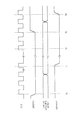
LPCバス124はまた、別々の制御線上でホスト102から各周辺デバイス104〜108に出力されることのある低電力または待機中の信号LPCPD#を含むことができる。図11に示すように、ホスト102は、時間t0にLPCPD#を非同期で(例えばローに)アサートし、それによって、周辺デバイス104〜108を低電力モードに入らせることができる。ホスト102によってアサートされたLPCPD#を認識する際、周辺デバイス104〜108は、いずれかのLPCトランザクションを停止し、LDRQ#信号を非活動状態にトライステートまたはドライブすることになる。周辺デバイス104〜108および/またはホスト102はまた、LAD[3:0]を既知の状態にトライステートまたはドライブできる。ホスト102はまた、LPCPD#をアサートした後でLFRAME#を既知の状態(ハイまたはロー)にドライブできる。低電力モードでは、LCLKを時間t1で切断でき、周辺デバイス104〜108がそれらの状態機械および/または他の論理を切断することができる。一実施形態の場合では、t0とt1の間の時間差は少なくとも30マイクロ秒ある。低電力モードの場合、LCLKは時間t2で非同期で再開でき、LPCPD#が時間t3でアサート解除されるまでのしばらくの間動作することができる。一実施形態の場合では、t2とt3の間の時間差は少なくとも100マイクロ秒である。次いで、時間t3から時間t4まで周辺デバイス104〜108をリセットするのに、LRESET#を使用できる。一実施形態の場合では、時間t3と時間t4の間の時間差は少なくとも60マイクロ秒である。
【0029】
ホスト102と周辺デバイス104〜108はまた、割込み信号(例えばSERIRQおよびSMI#)、追加クロック信号(例えばCLKRUN#)、および以下により詳細に記述する電力制御信号を含めた、ISAバスまたはPCIバスで使用される追加の側波帯の入力および/または出力信号も有することができる。
【0030】
一実施形態では、LPCバス124は、およそ6〜9本の信号線を使用することで、従来のISAバスまたはXバスのパーツまたはシステムに対する実質的な信号およびピン・カウントの節約を実現する。例えば、プラグアンドプレイのデバイスに通常使用される次のISAバスまたはXバスの信号はもはや必要とされない。D[7:0]、SA[15:0]、DREQ[3:0]、DACK#[3:0]、TC、IOR#、IOW#、IOCHRDY、IOCS16#、およびMEMCS16#がそれである。このことによって、バス、ホスト、および/または周辺デバイス上のおよそ30〜40個の信号が節約できる。一実施形態の場合、ISAバスまたはXバス互換の状況下で160本ものピンを有するパッケージが必要なこともあった全機能的なスーパーI/O周辺コントローラ・デバイスは、図1に示すようなLPCインタフェースの使用によって88本(またはそれ未満)のピンを有するパッケージを必要とするだけで済む。
【0031】
LPCバスは、メモリ読取り、メモリ書込み、入出力読取り、入出力書込み、DMA読取り、DMA書取り、バス・マスタ・メモリ読取り、バス・マスタ・メモリ書込み、バス・マスタ入出力読取り、バス・マスタ入出力書込みを含めた、メモリ、入出力、DMA、バス・マスタのトランザクションまたはサイクルを実行するために、LPCインタフェース112〜118によって使用されることが可能である。トランザクションのタイプは、ホスト102または周辺デバイス104、106、108によってLAD[3:0]でドライブされるサイクル・タイプおよび方向制御情報のフィールドに示されることが可能である。LAD[3:1]でコード化されるサイクル・タイプおよび制御情報の一実施形態を表2に示す。同じまたは異なる信号上の他のコード化も使用できる。
【0032】
表2
図2には、ホスト102のLPCインタフェース118の一実施形態であるLPCインタフェース200を示す。LPCインタフェース200は、表2のトランザクションを実行するために、LPCバス124上のアドレス、データ、制御情報を生成し、変換する。LPCインタフェース200は、ホスト102と周辺デバイス104〜108のうちの1つとの間のメモリ読取り、メモリ書込み、入出力読取り、および入出力書込みのLPCトランザクションを制御できる、メモリおよび入出力のLPC制御論理202を含む。メモリおよび入出力のLPC制御論理202は、特定のLPCトランザクションに必要な状態間の順番付けを行うため、かつ、LAD[3:0]、LFRAME#、および/またはLCLK上にアドレス、データ、または制御情報を生成するための、状態機械またはシーケンサを含むことができる。LAD[3:0]、LFRAME#、および/またはLCLK上に提供される情報は、論理208からLPCバス124に出力されるためにバス214に提供されることが可能である。
【0034】
一実施形態の場合、メモリおよび入出力のLPC制御論理202は、LPCメモリ・トランザクションまたは入出力トランザクションが1つまたは複数の信号216を介してLPC復号論理210と通信することによって実行される必要があることを決定する。LPC復号論理210は、メモリまたは入出力の読取りまたは書込み要求、および関連するアドレスを、ホスト102、ISAバス126、PCIバスまたはホスト・バス128から受信することができる。LPC復号論理はアドレスおよび信号メモリを復号化し、入出力LPC制御論理202はメモリまたは入出力LPCのトランザクションを開始する。あるいは、LPC復号論理210は、LPCインタフェース200の外、ただしホスト102の内部に位置付けることも可能である。オペレーティング・システム・ソフトウェアおよびアプリケーション・ソフトウェアに対するソフトウェア透過性をLPCトランザクションに持たせるのを補助するために、周辺デバイス104〜108に対して復号化されるアドレスの範囲は、以前のISAバスおよびXバスを使用するレガシー・ベースの周辺デバイスとの互換性を有するように定義できる。代替の実施形態の場合、メモリおよび入出力のLPCトランザクションの制御は、異なる制御回路内に分離することもできる。
【0035】
LPCインタフェース200はまた、ホスト102と入出力デバイス104および106のうちの1つとの間のDMA読取りおよび書込みのLPCトランザクションを制御するDMA LPC制御論理204も含む。DMA LPC制御論理204は、DMA LPCトランザクションに必要な状態間の順番付けを行うため、かつ、LAD[3:0]、LFRAME#、および/またはLCLK上にアドレス、データ、または制御情報を生成するため、かつ、DMA要求信号LDRQ0#およびLDRQ1#を受信するための、状態機械またはシーケンサを含むことができる。LAD[3:0]、LFRAME#、LDRQ0#、LDRQ1#、および/またはLCLKに提供される情報は、論理208およびバス214を介してLPCバス124間で提供されることができる。
【0036】
DMA LPC制御論理204は、ホスト102中に常駐できるDMAコントローラ212を介してホスト102およびメモリ110にインタフェースすることができる。DMA LPC制御論理204は、1つまたは複数の信号218を介してDMA制御論理212と通信することができる。一実施形態の場合、DMA制御論理212は、1つまたは複数の8237または8237互換のDMAコントローラを含むことができる。DMAコントローラ212は、入出力デバイスがそれを使用してホスト102を介してメイン・メモリ110と通信できるようなDMAチャネルの代わりに、ホスト102内の仲裁を実行することができる。
【0037】
LPCインタフェース200はまた、ホスト102と周辺デバイス104〜108の間の、バス・マスタ・メモリ読取りおよび書込みのLPCトランザクションと、バス・マスタ入出力読取りおよび書込みのLPCトランザクションとを制御するバス・マスタLPC制御論理206も含む。バス・マスタLPC制御論理206は、バス・マスタLPCトランザクションに必要な状態間の順番付けを行うため、かつ、LAD[3:0]、LFRAME#、および/またはLCLK上のアドレス、データ、または制御情報を生成するため、かつ、DMA要求信号LDRQ0#およびLDRQ1#を受信するための、状態機械またはシーケンサを含むことができる。LAD[3:0]、LFRAME#、LDRQ0#、LDRQ1#、および/またはLCLKに提供される情報は、論理208およびバス214を介してLPCバス124へ送り又はLPCバス124から受け取ることができる。
【0038】
論理208は、LPCバス124をLPCバス214にインタフェースするための1つまたは複数のバッファまたはトランシーバを含むことができる。あるいは、LPCインタフェース200はバス214を含まなくてもよく、論理208は、メモリおよび入出力のLPC制御論理202、DMA LPC制御論理204、およびバス・マスタLPC制御理論206の入力信号および出力信号に直接かつ個別に接続できる。この代替の実施形態の場合、論理208は、ホスト102の制御下で、LPCバス124と制御論理202、204、206との間で適したLPC信号を出力または入力する、セレクタ回路またはマルチプレクサ回路とすることができる。
【0039】
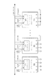
図3は、ホスト102と周辺デバイス104〜108の間で、メモリおよび/または入出力の書込みLPCトランザクションまたは読取りLPCトランザクションを実行するための1つまたは複数のLPCインタフェース112〜118が実施される状態図である。例えば、図3の状態図は、図2で示したメモリおよび入出力のLPC制御論理202の状態機械またはシーケンサによって使用されることが可能である。この状態図は、メモリ読取り、メモリ書込み、入出力読取り、入出力書込みのLPCトランザクションを実施する。他の実施形態の場合では、別々の状態機械がメモリ・トランザクションおよび入出力トランザクションを実施する。メモリ読取りおよび書込みのLPCトランザクションは、図4および図5の例示的なタイミング図を利用しながら述べる。
【0040】
最初に、ホスト102による、メモリ・デバイス108内のメモリ位置からの例示的なメモリ読取りLPCトランザクションを図3および図4を参照しながら述べる。このメモリ読取りLPCトランザクションは、例えば、ホスト102がメモリ・デバイス108からシステム起動情報を読み取ることによって実施できる。状態302では、LPCインタフェース118は、LFRAME#が(例えばハイに)アサート解除されていて、LPCトランザクションを実行しないアイドル状態である。ホスト102が、LPCバス124上のLFRAME#を(例えばローに)アサートすることによってLPCトランザクションを開始すると(例えば、制御論理202が、メモリ読取りLPCトランザクションが発生することを示す復号化された信号をLPC復号論理210およびホスト102から受信すると)、プロセスは状態304に移行する。ホスト102は、サイクルT0中にLAD[3:0]のLPCトランザクションの開始を示す開始制御情報をドライブすることができる。例えば、開始制御情報は表1に示すようにLAD[3:0]を0000とすることができる。
【0041】
次いでプロセスは状態306に移行し、ホスト102は、サイクルT1中にLAD[3:0]のサイクル・タイプおよび方向制御情報をドライブする。サイクル・タイプおよび方向制御情報は、LPCトランザクションがメモリ読取りトランザクションであることを周辺デバイス104〜108に示す。例えば、サイクル・タイプおよび方向制御情報は、表2に示すようにLAD[3:1]を010とする。
【0042】
次いでプロセスは状態308に移行し、ホスト102は、nクロック・サイクルT2中にLAD[3:0]の選択されたメモリ・デバイス108内のメモリ位置のアドレスをドライブする。アドレスは、図1のシステム100などのシステムによってサポートされるどんなビット長でもよく、いくつかのnクロック・サイクルT2にわたって送信される。一実施形態の場合、メモリ・アドレス空間は4ギガバイトで、32ビットのメモリ・アドレスを必要とすることがある。この実施形態では、8ニブル(32ビット)のアドレス情報をホスト102からメモリ・デバイス108に転送するために、8クロック・サイクルのアドレス情報が制御論理からLPCバス124に与えられる。アドレス情報は、最上位のニブルが先に提供されても、最下位のニブルが先に提供されてもよく、あるいはメモリ・デバイス108によって予想される他のどんな順番でもよい。
【0043】
代替の実施形態の場合、ホスト102は、後続のサイクル中にLAD[3:0]にサイズ制御情報を任意選択でドライブすることができる。一実施形態の場合、サイズ制御情報は、状態308で与えられるアドレスで開始され、メモリ・デバイス108から読み取られるべきメモリ・データのバイト数を示す。表3は、その後でLAD[3:0]を介して転送されるべきLAD[1:0]のバイト数をコード化する一実施形態を提供する。同じまたは異なるLAD信号線上の他のコード化も使用できる。
【0044】
表3
別の実施形態の場合、サイズ制御情報は、メモリ・データの2sizeバイト数がメモリ・デバイス108から、状態306で提供されるアドレスで開始され読み取られるべきであることを示すことがある。
【0046】
次いでプロセスは、転換(TAR)状態312に移行し、nクロック・サイクルT4中にLPCバス124の制御権をホスト102からメモリ・デバイス108に移す。一実施形態の場合、状態312は2クロックの幅を有する。最初のクロック・サイクルで、ホスト102は所定の制御情報(例えば1111)を使用してLAD[3:0]の信号線をドライブできる。第2のクロック・サイクルで、ホスト102はLAD[3:0]の信号線をトライステートにする。これらの信号線は、論理的に高い状態を維持できるようにこれらの信号線に付けられた弱いプルアップを有する。他の実施形態の場合、LAD[3:0]を転換するために、nは1クロック・サイクル、または2クロック・サイクルよりも大きいクロック・サイクルとすることができる。
【0047】
次いでプロセスは状態314に移行し、メモリ・デバイス108がLAD[3:0]の帯域内同期化制御情報をドライブする間、ホスト102はnクロック・サイクルT5で待機する。同期化制御情報は、メモリ・データがメモリ・デバイス108によって出力できるようになるまで待ち状態を追加するのに使用できる。このようにして、異なる速度またはアクセス時間のメモリ・デバイスが同じLPCバスに結合できる。従来は、いつデータの準備が整うかを示すために専用制御線上の専用制御信号が使用された(例えばISAバスまたはXバスのIOCHRDY)。これとは対照的に、メモリ・デバイス108は、LAD[3:0]の帯域内信号を使用して、追加の専用ピンまたは専用線を使用することなく待ち状態を挿入することができる。
【0048】
一実施形態の場合、同期化制御情報フィールドは2つの位相を有する。第1の位相は、要求されたデータにアクセスしながら、LAD[3:0]の第1の制御情報をドライブする(例えば0101または0110)。第2の位相は、そのデータがLPCバス124に出力される準備ができていることを示すLAD[3:0]の第2の制御情報をドライブする(例えばLAD[3:0]の0000)。ホスト102は同期化制御情報を監視し、いつ第2の情報が送信されるかを決定することができる。次いでホスト102は、後続のクロック・サイクルT6でメモリ・デバイス108によって出力されるデータがホスト102によって要求されたデータとなることを認識できる。一実施形態の場合、第1の制御情報は、メモリ・デバイス108がLAD[3:0]に相対的に多数の待ち状態(例えばおよそ20+待ち状態)をドライブすることを示すコード(例えばLAD[3:0]の0110)を有する。第1の制御情報はまた、メモリ・デバイス108がLAD[3:0]に相対的に少数の待ち状態(例えば1〜20待ち状態)を有することを示すコードを(例えばLAD[3:0]の0101)を有することもできる。一例では(以下の表4参照)、メモリ・デバイス108は、およそ1〜20クロック・サイクルでLAD[3:0]の0101の同期化データをそれぞれドライブし、次いで、要求されたデータの準備が整い、続くクロック・サイクルで出力されることを示すために、LAD[3:0]の0000の1サイクルをそれぞれドライブすることがある。
【0049】
待ち状態の数が多い場合、ホスト120は、状態320に入ることによってトランザクションの打切りを決定することができる。前述のように、ホスト102は、1つまたは複数のクロック・サイクルに対してLFRAME#をアサートし、LAD[3:0]の所定の打切り制御情報(例えば表1の1111)をドライブすることによってトランザクションを打ち切ることができる。
【0050】
制御情報の同期化フィールドはまた、LAD[3:0]の帯域内エラー・メッセージをホスト102のLPCインタフェース118に送るためにメモリ・デバイス108によって使用されることもある。エラー・メッセージは、同期化シーケンス中のいつでも送信できる。例えば、第1および第2の同期化制御情報を有する実施形態で第2の制御情報として送信することができる。エラー・メッセージは、例えば、要求されたデータが何らかの形で破損していたり、周辺デバイスが要求を理解しなかったり、無効な要求が出されたり、あるいは、周辺デバイスがパワー・ダウン・モードの間にまたはデータを出力する準備ができていないか出力できない他のモードの間に要求が出されたりしたことを示すことがある。一実施形態では、エラー・メッセージがメモリ読取りトランザクション中に送信された場合、そのデータは読出し後破棄される。
【0051】
表4は、上述の同期化制御情報に対するLAD[3:0]のコード化の一実施形態を提供する。他のコード化を使用することもできる。
【0052】
表4
代替の実施形態の場合、帯域内同期化制御情報は、待ち状態、エラー、あるいはすでに表4に記載されたまたは要約された他のいずれかの情報を通信するいずれかのシステム内の、汎用時分割多元バスを介するいずれか2つのデバイス(例えばホストと周辺デバイス)の間で使用できる。
【0054】
メモリ・デバイス108がそのデータをLPCバス124に出力する準備ができた時、プロセスは、LAD[3:0]で適切な同期化制御情報(例えば0000)を提供した後で、nクロック・サイクルT6にわたって状態316に移行する。状態316では、ホスト102はメモリ・デバイス108からLAD[3:0]に提供されたデータを読み取る。メモリ・デバイス108は、2クロック・サイクルにわたるバイト単位でLAD[3:0]にデータをドライブできる。2バイト転送の一実施形態の場合、第1のバイトは最初の2クロック・サイクルで出力され、第2のバイトは後続の2クロック・サイクルで出力されるであろう。データはメモリ・デバイス108によって各バイトに、低いニブルを先にしても、高いニブルを先にしても、または他のどんな形式によっても出力できる。同様に、メモリ・デバイス108によって出力されるバイトの各グループも、低いバイトを先にしても、高いバイトを先にしても、または他のどんな形式によっても出力できる。
【0055】
一実施形態の場合、同期化フィールド制御情報がバイト間に挿入されるように状態316と314の間でサイクリングすることによって、複数バイト読取りを実施することができる。代替の実施形態の場合、プロセスが状態316にある間に複数バイトのバースト読取りを読み取ることができる。この代替の実施形態では、メモリ・デバイス108は、状態314でLAD[3:0]の1100をドライブして、同期化制御情報がそれ以上データ・バイト間で伝達されないことを指示することができる。他の実施形態の場合、複数のまたはバーストのデータ読取りを指示するのに特定の同期化制御情報が必要でない場合がある。
【0056】
ホスト102で全データが読み取られた後、プロセスは転換(TAR)状態318に移行することができ、そこでLAD[3:0]の制御はクロック・サイクルT7中にホスト102に戻される。状態312と同様に、状態318も2クロック幅とすることができる。最初のクロック・サイクルで、メモリ・デバイス108は、所定の制御情報(例えば1111)によってLAD[3:0]をドライブする。第2のクロック・サイクルで、メモリ・デバイス108はLAD[3:0]の信号線をトライステートにできる。他の実施形態の場合、LAD[3:0]を転回させるためにnは1クロック・サイクル、または2クロック・サイクルより大きいサイクルとすることができる。
【0057】
図3および図5を参照しながら、ホスト102によるメモリ・デバイス108内のメモリ位置へのメモリ書込みLPCトランザクションの例を示す。このメモリ書込みLPCトランザクションは、例えばシステム起動情報をメモリ・デバイス108に書き込むためにホスト102によって実施される。状態302では、ホスト102はLPCトランザクションを実行しないアイドル状態である。ホスト102がLPCバス124上でLFRAME#をアサートすると(例えば制御論理202がLPC復号論理210およびホスト102から、メモリ読取りLPCトランザクションが行われることを示す復号化された信号を受領すると)、プロセスはLPCトランザクションを開始する。次いでプロセスは開始状態304に移行し、ホスト102はLAD[3:0]のLPCトランザクションの開始を示す開始制御情報をドライブする。例えば、開始制御情報は表1に示すように0000とすることができる。次いでプロセスは状態304に移行し、そのLPCトランザクションがメモリ書込みトランザクションであることを周辺デバイス104〜108に示すLAD[3:1]のサイクル・タイプおよび方向制御情報をT1サイクル中にドライブする。例えば、サイクル・タイプおよび方向制御情報は、表2に示すようにLAD[3:1]の011とすることができる。
【0058】
次いでプロセスは状態308に移行し、ホスト102は、LAD[3:0]の選択されたメモリ・デバイス108内のメモリ位置のアドレスをT2サイクル中にドライブする。前述のように、アドレスは図1のシステム100などのシステムによってサポートされるどんなビット長でもよく、n個のクロック・サイクルT2にわたって送ることができる。アドレス情報は、最上位のニブルを先にしても、最下位のニブルを先にしても、あるいはメモリ・デバイス108に予想できる他のどんな形式によっても提供することができる。
【0059】
代替の実施形態の場合、次いでホスト102は、LAD[3:0]にサイズ制御情報をサイクルT3中にドライブする。サイズ制御情報は、状態308で提供されるアドレスで開始されメモリ・デバイス108に書き込まれるメモリ・データのバイト数を示すことができる。
【0060】
次いでプロセスは状態310に移行し、ホスト102は、nクロック・サイクルT4で、LAD[3:0]を介してメモリ・デバイス108に適切なバイトのデータを書き込む。ホスト102は、2クロック・サイクルにわたるバイト単位でLAD[3:0]にデータをドライブできる。例えば、転送が16ビットすなわち2バイト転送である場合は、第1のバイトは最初の2クロック・サイクルで出力され、第2のバイトは次の2クロック・サイクルで出力される。データはホスト102によって各バイトに、低いニブルを先にしても、高いニブルを先にしても、または他のどんな形式によっても出力できる。同様に、ホスト102によって出力されるバイトの各グループも、低いバイトを先にしても、高いバイトを先にしても、または他のどんな形式によっても出力できる。ホスト102は1つまたは複数の(バースト)データ・バイトを状態310で書き込むことができる。
【0061】
次いでプロセスは転換(TAR)状態312に移行し、nクロック・サイクルT5中にLPCバス124の制御権をメモリ・デバイス108に移す。次いでプロセスは状態314に移行し、メモリ・デバイス108がLAD[3:0]帯域内同期化制御情報をクロック・サイクルT6でドライブする間、ホスト102はnクロック・サイクルで待機する。一実施形態の場合、同期化制御情報は1つまたは複数のクロック・サイクルとすることができ、メモリ・デバイス108中に書き込まれるデータの受領を通知するのに使用することができる(例えばLAD[3:0]の0000)。同期化制御情報はまた、データがメモリ・デバイス108中に書き込まれ記憶されるまで待ち状態を追加するのにも使用できる。この待ち状態の間に、メモリ・デバイス108は、表4に示すようなLAD[3:0]の短時間待ち状態の同期化制御情報または長時間待ち状態の同期化制御情報をドライブすることができる。メモリ・デバイス108がアドレスされたメモリ位置にデータを書き込み終えた時、メモリ・デバイス108はLAD[3:0]のレディ状態(例えば0000)をドライブすることができる。
【0062】
メモリ読取りLPCトランザクションの場合と同様に、メモリ・デバイス108はまた、制御情報の同期化フィールドを使用して、LAD[3:0]を介して帯域内エラー・メッセージ(例えば1010)をホスト102に送る。エラー・メッセージは例えば、書込みトランザクションが正しく行われなかったり、他の何らかのエラーが起こったことを示すことがある。
【0063】
次いでホスト102は転換(TAR)状態318に移行することができ、そこでLAD[3:0]の制御はnクロック・サイクルT7中にホスト102へ戻されることが可能である。
【0064】
図6は、ホスト102と周辺デバイス104〜108の間で、メモリおよび/または入出力の書込みLPCトランザクションおよび読み取りLPCトランザクションを実行するための1つまたは複数のLPCインタフェース112〜118の状態図の別の実施形態である。例えば図6の状態図は、図2に示すメモリおよび入出力のLPC制御論理202の状態機械またはシーケンサによって使用されることが可能である。この状態図は、メモリ読取りおよびメモリ書込みのLPCトランザクションを実行する。図7および図8の例示的なタイミング図を利用しながら、メモリ読取りおよびメモリ書込みのLPCトランザクションを述べる。
【0065】
最初に、ホスト102による、メモリ・デバイス108中のメモリ位置からの例示的なメモリ読取りLPCトランザクションを、図6および図7を参照しながら記述する。メモリ読取りLPCトランザクションは、例えば、ホスト102がメモリ・デバイス108からシステム起動情報を読み取ることによって実行できる。状態602では、LPCインタフェース118は、LFRAME#が(例えばハイに)アサート解除されており、LPCトランザクションを実行しないアイドル状態である。ホスト102がLFRAME#を(例えばローに)LPCバス124上でアサートすることによってLPCトランザクションを開始すると(例えば制御論理202がLPC復号論理210およびホスト102から、メモリ読取りLPCトランザクションが行われることを示す復号化された信号を受領すると)、プロセスは状態604に移行する。ホスト102は、サイクルT0中にLAD[3:0]のLPCメモリ読取りトランザクションの開始を示す開始制御情報をドライブすることができる。例えば、開始制御情報は表1に示すようにLAD[3:0]の1101とすることができる。
【0066】
次いでプロセスはデバイス選択(IDSEL)状態606に移行し、ホスト102は、LAD[3:0]のデバイス選択制御情報をドライブして、メモリ読取りトランザクション用の特定のメモリ・デバイスを選択する。一実施形態の場合、LPCバス124に結合されるメモリ・デバイスは、外部結線接続による、または内部抵抗器ベースの識別を有することがある。図9に、結線接続のメモリ・デバイスの識別の一実施形態を示す。メモリ・デバイス900は、入力線10、11、12、13上にそれぞれ0000の識別を有する。メモリ・デバイス901は、入力線10、11、12、13上にそれぞれ0001の識別を有する。メモリ・デバイス915は、入力線10、11、12、13上にそれぞれ1111の識別を有する。結線接続の入力線をいくつでも使用して、バイナリ形式または他の何らかの形式によってメモリ・デバイスをいくつでも識別または選択することができる。LPCバス124に結合される各メモリ・デバイスは、デバイス選択制御情報をその結線接続の識別と比較し、そのLPCメモリ読取り(または書込み)トランザクションが自身に向けられたものかどうかを決定する。メモリ・トランザクションが自身に向けられたものでない場合、メモリ・デバイスはパワー・ダウン状態(例えばアイドル状態602)に入ることがある。
【0067】
次いでプロセスは状態608に移行し、ホスト102は、LAD[3:0]の、選択されたメモリ・デバイス108中のメモリ位置のアドレスをnクロック・サイクルT2中にドライブする。アドレスは、図1のシステム100のようなシステムにサポートされるどんなビット長でもよく、n個のクロック・サイクルT2にわたって送られる。一実施形態の場合、メモリ・アドレス空間は256キロバイトで、28ビットのメモリ・アドレスを必要とすることがある。この実施形態では、ホスト102からメモリ・デバイス108に7ニブル(28ビット)のアドレス情報を転送するために、7クロック・サイクルのアドレス情報が制御論理からLPCバス124に提供される。アドレス情報は、最上位のニブルが先でも、最下位のニブルが先でも、またはメモリ・デバイス108に予想される他のどんな順番でも提供することができる。
【0068】
次いでプロセスは状態610に移行し、ホスト102は、クロック・サイクルT3中にLAD[3:0]にサイズ制御情報をドライブする。一実施形態の場合、サイズ制御情報は、状態606で提供されるアドレスで開始され、メモリ・デバイス108から読み取られるべきメモリ・データのバイト数を示す。表6は、バイト数をコード化する一実施形態を提供する。別の実施形態の場合、サイズ制御情報は、メモリ・データの2sizeバイト数がメモリ・デバイス108から、状態608で提供されるアドレスで開始され読み取られるべきであることを示すことがある。
【0069】
一実施形態の場合、データ転送はホスト102によって2sizeの境界に配列されることがある。例えば、サイズ・フィールドがLAD[3:0]の0100と等しい場合、その動作は16バイトの境界に配列され、メモリ・デバイス108は、16バイトに配列されたアドレスで始まる16バイトのデータを受領または送出しなければならない。別の実施形態では、データ転送は、表3のようなサイズ境界に配列されることがある。例えば、サイズがLAD[3:0]の0010と等しい場合、その動作は16ビット境界または語境界に整列され、メモリ・デバイス108は、16ビットまたは語に配列されたアドレスで始まる16ビットのデータを受領または送出しなければならない。
【0070】
次いでプロセスは転換(TAR)状態614に移行して、nクロック・サイクルT4中にLPCバス124の制御権をホスト102からメモリ・デバイス108に移す。次いでプロセスは状態616に移行し、そこでメモリ・デバイス108がLAD[3:0]の帯域内同期化制御情報をドライブする間、ホスト102はnクロック・サイクルT5で待機する。図3の状態314に関連して上記に述べたように、同期化制御情報はメモリ・トランザクションに待ち状態を追加するのに使用することができる。待ち状態の数が多い場合、ホスト102は、状態622に入ることによってトランザクションを打ち切る決定をすることができる。前述のように、ホスト102は、1つまたは複数のクロック・サイクルにLFRAME#をアサートし、LAD[3:0]の所定の打切り制御情報(例えば表1の1111)をドライブすることによってトランザクションを打ち切ることができる。
【0071】
図3の状態314に関連して上記に述べたように、制御情報の同期化フィールドもまた、ホスト102のLPCインタフェース118にLAD[3:0]の帯域内エラー・メッセージを送るために、メモリ・デバイス108によって使用されることが可能である。上記の表4は、上述の同期化制御情報に対するLAD[3:0]のコード化の一実施形態を提供する。他のコード化を使用することも可能である。
【0072】
代替の実施形態の場合、帯域内同期化制御情報は、待ち状態、エラー、あるいはすでに表4に記載されたまたは要約された他のいずれかの情報を通信するいずれかのシステム内の、汎用時分割多元バスを介するいずれか2つのデバイス(例えばホストと周辺デバイス)の間で使用できる。
【0073】
メモリ・デバイス108がそのデータをLPCバス124に出力する準備ができた時、LAD[3:0]で適切な同期化制御情報(例えば0000)を提供した後で、プロセスはnクロック・サイクルT6にわたって状態618に移行する。状態618では、ホスト102はメモリ・デバイス108からLAD[3:0]に提供されたデータを読み取る。メモリ・デバイス108は、2クロック・サイクルにわたるバイト単位でLAD[3:0]にデータをドライブできる。データはメモリ・デバイス108によって各バイトに、低いニブルを先にしても、高いニブルを先にしても、または他のどんな形式によっても出力できる。同様に、メモリ・デバイス108によって出力されるバイトの各グループも、低いバイトを先にしても、高いバイトを先にしても、またはホスト102に予想できる他のどんな形式によっても出力できる。
【0074】
一実施形態の場合、同期化フィールド制御情報がバイト間に挿入されるように状態618と616の間でサイクリングすることによって、複数バイト読取りを実施することができる。代替の実施形態の場合、ホスト102が状態618にある間に複数バイトのバースト読取りを読み取ることができる。この代替の実施形態では、メモリ・デバイス108は、状態616でLAD[3:0]の1100をドライブして、同期化制御情報がそれ以上データ・バイト間で伝達されないことを指示することができる。他の実施形態の場合、複数のまたはバーストのデータ読取りを指示するのに特定の同期化制御情報が必要でない場合がある。
【0075】
ホスト102で全データが読み取られた後、プロセスは転換(TAR)状態620に移行することができ、そこでLAD[3:0]の制御はnクロック・サイクルT7中にホスト102に戻されることが可能である。状態614と同様に、状態620も2クロック幅とすることができる。最初のクロック・サイクルで、メモリ・デバイス108は、所定の制御情報(例えば1111)によってLAD[3:0]の線をドライブする。第2のクロック・サイクルで、メモリ・デバイス108はLAD[3:0]の線をトライステートにできる。他の実施形態の場合、LAD[3:0]を転回させるためにnは1クロック・サイクル、または2クロック・サイクルより大きいサイクルとすることができる。
【0076】
図6および図8を参照しながら、ホスト102によるメモリ・デバイス108内のメモリ位置へのメモリ書込みLPCトランザクションの例を示す。このメモリ書込みLPCトランザクションは、例えばシステム起動情報をメモリ・デバイス108に書き込むためにホスト102によって実施される。状態602では、ホスト102はLPCトランザクションを実行しないアイドル状態である。ホスト102がLPCバス124上でLFRAME#をアサートすると(例えば制御論理202がLPC復号論理210およびホスト102から、メモリ読取りLPCトランザクションが行われることを示す復号化された信号を受領すると)、プロセスはLPCトランザクションを開始する。次いでプロセスは開始状態604に移行し、ホスト102はLAD[3:0]の開始制御情報をクロック・サイクルT0中にドライブする。開始制御情報は、メモリ書込みLPCトランザクションの開始を示す。例えば、ホスト102は、表1に示すようなLAD[3:0]に開始制御情報1110をドライブすることができる。次いでプロセスはデバイス選択(IDSEL)状態606に移行し、そのメモリ書込みトランザクションに対する特定のメモリ・デバイスを識別または選択する。
【0077】
次いでプロセスは状態608に移行し、ホスト102は、LAD[3:0]の選択されたメモリ・デバイス108内のメモリ位置のアドレスをnクロック・サイクルT2中にドライブする。前述のように、アドレスは図1のシステム100などのシステムによってサポートされるどんなビット長でもよく、nクロック・サイクルT2にわたって送ることができる。アドレス情報は、最上位のニブルを先にしても、最下位のニブルを先にしても、あるいはメモリ・デバイス108に予想できる他のどんな形式によっても提供することができる。
【0078】
次いでプロセスは状態610に移行し、ホスト102はクロック・サイクルT3中にLAD[3:0]にサイズ制御情報をドライブする。次いでプロセスは状態612に移行し、ホスト102は、nクロック・サイクルT4中にLAD[3:0]を介してメモリ・デバイス108に適切なバイトのデータを書き込む。ホスト102は、2クロック・サイクルにわたるバイト単位でLAD[3:0]にデータをドライブできる。例えば、転送が16ビットすなわち2バイト転送である場合は、第1のバイトは最初の2クロック・サイクルで出力され、第2のバイトは次の2クロック・サイクルで出力される。各バイトに対して、データはホスト102によって、低いニブルを先にしても、高いニブルを先にしても、または他のどんな形式によっても出力できる。同様に、ホスト102によって出力されるバイトの各グループも、低いバイトを先にしても、高いバイトを先にしても、または他のどんな形式によっても出力できる。ホスト102は1つまたは複数の(バースト)データ・バイトを状態612で書き込むことができる。
【0079】
次いでプロセスは転換(TAR)状態614に移行し、nクロック・サイクルT5中にLPCバス124の制御権をメモリ・デバイス108に移す。次いでプロセスは状態616に移行し、メモリ・デバイス108がLAD[3:0]に帯域内同期化制御情報をクロック・サイクルT6中にドライブする間、ホスト102はnクロック・サイクルで待機する。一実施形態の場合、同期化制御情報は1つまたは複数のクロック・サイクルとすることができ、メモリ・デバイス108中に書き込まれるデータの受領を通知するのに使用することができる(例えばLAD[3:0]の0000)。同期化制御情報はまた、データがメモリ・デバイス108中に書き込まれ記憶されるまで待ち状態を追加するのにも使用できる。メモリ読取りLPCトランザクションに伴って、メモリ・デバイス108は、制御情報の同期化フィールドを使用して、LAD[3:0]を介して(例えば1010)ホスト102に帯域内エラー・メッセージを送ることもできる。エラー・メッセージは例えば、書込みトランザクションが正しく行われなかったり、他の何らかのエラーが起こったことを示すことがある。同期化制御情報のコード化の一実施形態を表4に示す。
【0080】
次いで、ホスト102は転換(TAR)状態618に移行することができ、そこでnクロック・サイクルT7中にLAD[3:0]の制御がホスト102に戻されることが可能である。
【0081】
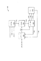
図10に、メモリ・デバイス108の一実施形態であるメモリ・デバイス1000を示す。メモリ・デバイス1000は、SRAM、DRAM、EPROM、EEPROM、ROMなどの揮発性および不揮発性メモリ・デバイスを含む、どんなタイプのメモリ・デバイスとすることもできるメモリ1010を含む。メモリ1000は、いずれかの揮発性または不揮発性メモリ・デバイスを実装するのに必要な、制御回路およびメモリ・エレメントを含む。一実施形態の場合、メモリ1000は、それに結合された制御エンジンを有し、フラッシュ・メモリ・セルのアレイのプログラミング、読取り、消去を制御する不揮発性(例えばフラッシュ)メモリ・デバイスである。
【0082】
メモリ・デバイス1000はまた、入出力ラッチ1002、制御論理1004、状態機械1006、およびメモリ制御論理1008を有するLPCインタフェース116の一実施形態も含む。制御論理1004は、LPC入力信号LFRAME#、LCLK、および/またはLRESET#を受け取り、これらの信号の指示を信号線1012上の制御信号を介して状態機械またはシーケンサ1006に与える。一実施形態の場合、入出力ラッチ1002は、アドレス、制御、データの情報をLAD[3:0]から受領し、かつLAD[3:0]へ出力する。入出力ラッチ1002は、バス1014を介して、LAD[3:0]から受け取ったアドレス、データ、制御情報を状態機械1006およびメモリ制御論理1008に渡す。入出力ラッチ1002はLAD[3:0]から受領した様々なニブルのデータを集約することができる。
【0083】
バス1014および線1012から受け取ったアドレス、データ、制御情報によって、状態機械1006は、メモリ・デバイス1000がLPCバス124を介してホスト102と通信できるように、またはバス・マスタLPCトランザクション中に入出力デバイス104およびメモリ1010と通信できるように、メモリ・デバイス1000のLPCインタフェースを制御する。状態機械1006の一実施形態は図3に示したものである。状態機械1006の別の実施形態は図6に示したものである。
【0084】
状態機械1006はメモリ制御論理1008と共に動作して、必要な制御、アドレス、データの情報をメモリ1010に提供する。メモリ制御論理1008は、メモリ1010が書込みまたは読取りトランザクションを実行するのに必要な制御信号を線1018上に、アドレス信号を線1020上に、データ信号を線1022上に生成する。線1018上の制御信号には、アドレス・ストローブ信号(例えばRASおよび/またはCAS)、チップ・イネーブルまたはチップ選択信号(例えばCEおよび/またはCS)、書込みおよび読取りイネーブル信号、リセット信号、パワー・ダウン信号などが含まれることがある。
【0085】
メモリ書込みトランザクションが行われることを状態機械1006が決定すると、状態機械1006は、メモリ制御論理が線1020を介して線1018上の適切な制御信号と共にメモリ1010に提供できるように、いつアドレス情報がバス1014上に存在するかを線1016を介して示すことができる。その後、状態機械1006は、メモリ制御論理が線1022を介して線1018上の適切な制御信号と共にメモリ1010に提供できるように、いつデータ情報がバス1014上に存在するかを線1016を介して示すことができる。同様に、メモリ読取りトランザクションが行われることを状態機械1006が決定すると、状態機械1006は、メモリ制御論理が線1020を介して線1018上の適切な制御信号と共にメモリ1010に提供できるように、いつアドレス情報がバス1014上に存在するかを線1016を介して示すことができる。その後、状態機械1006は、いつ要求されたデータがメモリ1010から線1026を介して入出力ラッチ1002およびLAD[3:0]に出力されるべきかを、線1016を介して示すことができる。メモリ制御論理1008は、1つまたは複数の入出力制御信号を線1024上に発信して、入出力ラッチ1002の双方向状態を制御することができる。例えば、データがメモリ1010から読み取られる時、メモリ制御論理1008は線1024を介して出力イネーブル信号を発信することができる。
【0086】
前述の明細書で、本発明はその具体的な実施形態が述べられた。しかし、添付の特許請求の範囲で述べる本発明のより広い趣旨および目的から逸脱することなく、様々な修正および変更がそれになされうることは明白であろう。したがって、本明細書および図面は、限定的なものではなく例示的なものである。
【図面の簡単な説明】
【図1】 ロー・ピン・カウント(LPC)のバスを有するコンピュータ・システムの一実施形態を示す図である。
【図2】 LPCインタフェースの一実施形態を示す図である。
【図3】 メモリ・トランザクションおよび入出力トランザクションを実施するための状態機械図の一実施形態を示す図である。
【図4】 LPCメモリ読取りトランザクションの一実施形態を示す図である。
【図5】 LPCメモリ書込みトランザクションの一実施形態を示す図である。
【図6】 メモリ・トランザクションおよび入出力トランザクションを実施するための状態機械図の別の実施形態を示す図である。
【図7】 LPCメモリ読取りトランザクションの別の実施形態を示す図である。
【図8】 LPCメモリ書込みトランザクションの別の実施形態を示す図である。
【図9】 メモリ・デバイスの選択方式の一実施形態を示す図である。
【図10】 メモリ・デバイスに対するLPCインタフェースの一実施形態を示す図である。
【図11】 低電力モードの動作に対するタイミング図の一実施形態を示す図である。[0001]
(Cross-reference of related applications)
This application US Patent Application No. _ "I / O TRANSACTIONS ON A LOW PIN COUNT BUS" issue,_ US patent application entitled “DIRECT MEMORY ACCESS (DMA) TRANSACTIONS ON A LOW PIN COUNT BUS” Issue, and US patent application entitled “BUS MASTER TRANSACTIONS ON A LOW PIN COUNT BUS” The related application of No. Each application identified above is assigned to the same assignee as the present application.
[0002]
(Field of Invention)
The present invention relates to computer systems. More particularly, the present invention relates to communication between different types of devices on a low pin count bus of a computer system.
[0003]
(Background of the Invention)
Conventional legacy-based computer systems include various peripheral and storage devices that communicate with the system chipset or processor via an Industry Standard Architecture (ISA) bus or an expansion bus (X bus). The system chipset or processor can be an input / output (I / O) device or input / output controller such as a parallel port controller, serial port controller, super I / O controller, floppy disk controller, keyboard controller, etc. Used to interface a chipset or processor to legacy based peripheral devices including devices and memory devices such as non-volatile memory devices that store basic input-outout services (BIOS) information, for example In order to support an ISA bus signal or an X bus signal, it must have a large number of pins (eg, approximately 50 to 70 pins) and associated circuitry.
[0004]
The large number of pins required to support the ISA bus and X bus standards generally increases the overall system cost. For example, a large package is required for a chipset or processor. Higher pin count packages are generally more costly than lower pin count packages and are generally more susceptible to manufacturing quality and reliability issues during the package assembly and system integration process. Furthermore, the higher the pin count, the more surface area is required on the printed circuit board (PCB) on which the computer system is mounted. Therefore, it would be desirable to replace the ISA bus or X bus of a computer system with a bus that supports the same type of peripheral device and that utilizes a relatively small number of pins or signal lines.
[0005]
The ISA bus and X bus standards also limit the size of the memory address space or I / O address space to a memory address space or I / O address space of 24 bits, or approximately 16 megabytes. Since some processors and chipsets can support 32-bit or 64-bit address spaces, aliasing has been required to convert a processor address space to an ISA address space. Aliasing can create significant overhead that can negatively impact the performance of the computer system. Therefore, it would be desirable to replace the ISA bus and X bus standards with a bus that is compatible with the address space of a processor or chipset and that can support potentially unlimited address spaces.
[0006]
The ISA bus and X bus standards also have the disadvantage of being asynchronous. This generally complicates the design of components that need to generate and respond to ISA and X bus signals. Therefore, it would be desirable to replace the ISA bus and X bus standards with a bus that can support synchronous communication between components, thereby generally reducing the complexity of the bus interface circuit.
[0007]
(Summary of Invention)
A system having a bus coupled to a host and a memory device is described. The bus has a plurality of general-purpose signal lines that carry time-division multiplexed addresses, data, and control information. The memory device stores system startup information and can communicate this information with the host via the bus.
[0008]
Other features and advantages of the present invention will be apparent from the accompanying drawings and from the detailed description that follows below.
[0009]
The features and advantages of the invention are illustrated by way of non-limiting example in the accompanying drawing figures, in which like references indicate like components.
[0010]
(Detailed explanation)
A computer system using a low pin count (LPC) bus is disclosed. The LPC bus can be an alternative to the ISA bus or X bus in a computer system and includes a host such as a processor or chipset and peripheral devices such as an input / output device, an input / output controller device, and a memory device. Provides a communication mechanism between In one embodiment, the LPC bus is at almost all times to perform memory transactions, I / O transactions, direct memory access (DMA) transactions, bus master transactions between the host and peripheral devices. It will include general purpose signal lines that carry the division multiplexed address, data, and control information.
[0011]
The intended advantage of the LPC bus is that it uses much fewer signal lines (eg, approximately 6 to 6) to perform all the functions previously performed by approximately 50 to 70 signal lines of the ISA bus and X bus standards. Only 8 signal lines). Because the number of signal lines to the LPC bus can be much reduced compared to the ISA and X bus standards, the number of pins required on a computer system chipset or processor to support the LPC bus is greatly reduced. it can. Similarly, the LPC interface provided in each peripheral device can similarly use a small number of pins to interface to the chipset or processor via the LPC bus. This allows for lower packaging costs for component manufacturers and lower system costs for computer system manufacturers. This also allows higher quality and more reliable packaging and system integration. The LPC bus can also be used as a replacement for other system buses to reduce the pin count of packages coupled to the bus.
[0012]
Another intended advantage of the LPC bus is that the memory address space and / or the input / output address space is not limited to a specific number of address lines in the communication bus, but the LPC bus may be in any address space. All address signals that need to be addressed can be conveyed serially. Thus, conventional aliasing of the memory address space and / or the input / output address space can be avoided.
[0013]
Another intended advantage of the LPC bus is that the LPC interface logic and / or software that can interface a chipset or processor to a peripheral device provides software compatibility with existing computer systems that employ the ISA bus or X bus standards. It is to have. That is, no special drivers or settings are required for operating system software or application programs to operate on the LPC bus system for the ISA bus or X bus standards.
[0014]
Another intended advantage of the LPC bus is that it can be a synchronous bus, where the LPC interface circuitry in the host and peripheral devices is a generally less complex circuit than the asynchronous bus interface structure.
[0015]
The LPC bus and associated support circuitry can also be incorporated into other systems including printers, digital cameras, communication systems (eg, modems, cellular telephone systems, pagers, digital answering systems).
[0016]
FIG. 1 illustrates one embodiment of a
[0017]
Input /
[0018]
The memory device 108 is a peripheral device that can address the memory space. For example, the memory device 108 may be any type of volatile, such as DRAM, SRAM, flash memory, EPROM (electrically programmable ROM), EEPROM (electrically erasable PROM), magnetic storage media, optical storage media, etc. Memory or non-volatile memory can also be included. Memory device 108 can store system startup code, control code, operating system data, application code, program data, or a scratch pad for host 102 or I /
[0019]
Each of the host 102 and
[0020]
The LAD [3: 0] signal line is a general-purpose signal line that carries time-division multiplexed address, data, and control information between the host 102 and the
[0021]
LCLK is a clock signal that can be generated by the
[0022]
LFRAME # is generated by the
[0023]
Table 1
LFRAME # is used to abort or terminate an LPC transaction. For example, each
[0025]
In an alternative embodiment, LFRAME # is used for transactions such as memory transactions, I / O transactions, bus master transactions, DMA transactions between any two devices (eg, host and peripheral devices) in any system. It can also be used as an independent control signal on an independent signal line (away from the bus) that communicates the start or abort.
[0026]
The
[0027]
Input /
[0028]
The
[0029]
Host 102 and peripheral devices 104-108 are also on the ISA or PCI bus, including interrupt signals (eg, SERIRQ and SMI #), additional clock signals (eg, CLKRUN #), and power control signals described in more detail below. It may also have additional sideband input and / or output signals used.
[0030]
In one embodiment, the
[0031]
LPC bus is memory read, memory write, I / O read, I / O write, DMA read, DMA write, bus master memory read, bus master memory write, bus master I / O read, bus master input It can be used by LPC interfaces 112-118 to perform memory, I / O, DMA, bus master transactions or cycles, including output writes. The type of transaction may be indicated in the cycle type and direction control information fields driven by LAD [3: 0] by the host 102 or
[0032]
Table 2
FIG. 2 shows an
[0034]
For one embodiment, the memory and I / O
[0035]
The
[0036]
The DMA
[0037]
The
[0038]
The
[0039]
FIG. 3 illustrates a state in which one or more LPC interfaces 112-118 for performing memory and / or input / output write LPC transactions or read LPC transactions between the host 102 and the peripheral devices 104-108 are implemented. FIG. For example, the state diagram of FIG. 3 may be used by the memory and input / output
[0040]
First, an exemplary memory read LPC transaction from the memory location in the memory device 108 by the host 102 will be described with reference to FIGS. This memory read LPC transaction can be implemented, for example, by the host 102 reading system boot information from the memory device 108. In
[0041]
The process then transitions to
[0042]
The process then transitions to
[0043]
In an alternative embodiment, the host 102 can optionally drive size control information to LAD [3: 0] during subsequent cycles. For one embodiment, the size control information starts at the address given in
[0044]
Table 3
In another embodiment, the size control information is 2 of the memory data.sizeThe number of bytes may indicate from memory device 108 that it should start and read at the address provided in
[0046]
The process then transitions to a transition (TAR)
[0047]
The process then transitions to
[0048]
For one embodiment, the synchronization control information field has two phases. The first phase drives the first control information of LAD [3: 0] while accessing the requested data (eg 0101 or 0110). The second phase drives LAD [3: 0] second control information indicating that the data is ready to be output to the LPC bus 124 (eg, 0000 for LAD [3: 0]). . The host 102 can monitor the synchronization control information and determine when the second information is transmitted. The host 102 can then recognize that the data output by the memory device 108 in the subsequent clock cycle T6 is the data requested by the host 102. In one embodiment, the first control information includes a code (eg, LAD [3] indicating that the memory device 108 drives a number of wait states (eg, approximately 20+ wait states) relative to LAD [3: 0]. 3: 0] 0110). The first control information also includes a code (eg, LAD [3: 0] indicating that the memory device 108 has a relatively small number of wait states (eg, 1-20 wait states) in LAD [3: 0]. 0101). In one example (see Table 4 below), the memory device 108 drives each LAD [3: 0] 0101 synchronized data in approximately 1-20 clock cycles, and then the requested data is ready. In order to show that it is aligned and output in the following clock cycle, it may drive one cycle of 0000 of LAD [3: 0].
[0049]
If the number of wait states is large, the host 120 can decide to abort the transaction by entering the
[0050]
The synchronization field of the control information may also be used by the memory device 108 to send a LAD [3: 0] in-band error message to the
[0051]
Table 4 provides an embodiment of LAD [3: 0] encoding for the synchronization control information described above. Other encodings can also be used.
[0052]
Table 4
In an alternative embodiment, the in-band synchronization control information is a generic time in any system that communicates a wait state, error, or any other information already listed or summarized in Table 4. It can be used between any two devices (for example, a host and a peripheral device) via a divided multiple bus.
[0054]
When the memory device 108 is ready to output its data to the
[0055]
For one embodiment, a multi-byte read can be performed by cycling between
[0056]
After all data has been read at host 102, the process can transition to a transition (TAR)
[0057]
With reference to FIGS. 3 and 5, an example of a memory write LPC transaction by the host 102 to a memory location in the memory device 108 is shown. This memory write LPC transaction is performed, for example, by the host 102 to write system boot information to the memory device 108. In
[0058]
The process then transitions to
[0059]
In an alternative embodiment, the host 102 then drives size control information on LAD [3: 0] during cycle T3. The size control information can indicate the number of bytes of memory data written to the memory device 108 starting at the address provided in
[0060]
The process then transitions to
[0061]
The process then transitions to a transition (TAR)
[0062]
As with the memory read LPC transaction, the memory device 108 also uses the control information synchronization field to send an in-band error message (eg, 1010) to the host 102 via LAD [3: 0]. send. The error message may indicate, for example, that the write transaction was not performed correctly or that some other error occurred.
[0063]
The host 102 can then transition to the transition (TAR)
[0064]
FIG. 6 illustrates another state diagram of one or more LPC interfaces 112-118 for performing memory and / or input / output write LPC transactions and read LPC transactions between the host 102 and peripheral devices 104-108. It is an embodiment. For example, the state diagram of FIG. 6 may be used by the state machine or sequencer of the memory and input / output
[0065]
Initially, an exemplary memory read LPC transaction from the memory location in the memory device 108 by the host 102 will be described with reference to FIGS. A memory read LPC transaction can be performed, for example, by the host 102 reading system boot information from the memory device 108. In
[0066]
The process then transitions to a device selection (IDSEL)
[0067]
The process then transitions to
[0068]
The process then transitions to
[0069]
In one embodiment, data transfer is performed by the host 102 with 2sizeMay be arranged at the boundary. For example, if the size field is equal to 0100 in LAD [3: 0], the operation is aligned on a 16-byte boundary and the memory device 108 receives 16 bytes of data starting at the address aligned in 16 bytes. Or must be sent out. In another embodiment, data transfers may be arranged on size boundaries as in Table 3. For example, if the size is equal to 0010 of LAD [3: 0], the operation is aligned to a 16-bit boundary or word boundary and the memory device 108 is 16-bit data starting at an address arranged in 16 bits or words. Must be received or sent out.
[0070]
The process then transitions to a transition (TAR)
[0071]
As described above in connection with
[0072]
In an alternative embodiment, the in-band synchronization control information is a generic time in any system that communicates a wait state, error, or any other information already listed or summarized in Table 4. It can be used between any two devices (for example, a host and a peripheral device) via a divided multiple bus.
[0073]
When the memory device 108 is ready to output its data to the
[0074]
For one embodiment, a multiple byte read can be performed by cycling between
[0075]
After all data has been read at host 102, the process can transition to a transition (TAR)
[0076]
With reference to FIGS. 6 and 8, an example of a memory write LPC transaction by the host 102 to a memory location in the memory device 108 is shown. This memory write LPC transaction is performed, for example, by the host 102 to write system boot information to the memory device 108. In
[0077]
The process then transitions to
[0078]
The process then transitions to
[0079]
The process then transitions to a transition (TAR)
[0080]
The host 102 can then transition to a transition (TAR) state 618 where control of LAD [3: 0] can be returned to the host 102 during n clock cycles T7.
[0081]
FIG. 10 illustrates a
[0082]
[0083]
Depending on the address, data, and control information received from
[0084]
The
[0085]
When the
[0086]
In the foregoing specification, the invention has been described with reference to specific embodiments. However, it will be apparent that various modifications and changes may be made thereto without departing from the broader spirit and scope of the invention as set forth in the appended claims. Accordingly, the specification and drawings are illustrative rather than limiting.
[Brief description of the drawings]
FIG. 1 illustrates one embodiment of a computer system having a low pin count (LPC) bus.
FIG. 2 is a diagram illustrating an embodiment of an LPC interface.
FIG. 3 illustrates one embodiment of a state machine diagram for performing memory transactions and I / O transactions.
FIG. 4 illustrates one embodiment of an LPC memory read transaction.
FIG. 5 illustrates one embodiment of an LPC memory write transaction.
FIG. 6 illustrates another embodiment of a state machine diagram for performing memory transactions and I / O transactions.
FIG. 7 illustrates another embodiment of an LPC memory read transaction.
FIG. 8 illustrates another embodiment of an LPC memory write transaction.
FIG. 9 illustrates an embodiment of a memory device selection scheme.
FIG. 10 illustrates one embodiment of an LPC interface to a memory device.
FIG. 11 illustrates one embodiment of a timing diagram for operation in a low power mode.
Claims (3)
時分割多重化されたアドレス、データ、制御情報を搬送する複数の汎用信号線を有し且つ、前記メモリ・デバイスに対する低電力モードを示す制御信号を搬送するための独立した制御信号線を有するバスを備え、
前記バスに結合されたホストにして、そのホストと前記メモリ・デバイスとの間での前記システム起動情報の一部の通信を行うメモリ・トランザクションを示す制御情報を、前記バスを介して前記メモリ・デバイスに書き込むホストを備える
ことを特徴とするシステム。A memory device for storing system startup information including instructions for configuring or booting components in the system;
A bus having a plurality of general-purpose signal lines for carrying time-division multiplexed addresses, data, and control information, and an independent control signal line for carrying a control signal indicating a low power mode for the memory device With
Control information indicating a memory transaction for communicating a part of the system activation information between the host and the memory device is transmitted to the memory coupled to the host coupled to the bus via the bus. A system comprising a host for writing to a device.
前記メモリ・デバイスへの制御信号にして、メモリ・トランザクションの開始を示す制御信号を、前記ホストが前記制御線上にアサートするステップと、
当該メモリ・トランザクションが前記ホストから前記メモリ・デバイスへのデータ・ユニットの書き込みであることを示す書き込みトランザクション制御情報にして、前記メモリ・デバイスに対する書き込みトランザクション制御情報を、前記ホストが前記複数の汎用信号線にドライブするステップと、
前記メモリ・デバイスへのアドレス情報にして、前記データ・ユニットを書き込むべき前記メモリ・デバイス内のアドレスを示すアドレス情報を、前記ホストが前記複数の汎用信号線にドライブするステップと、
前記メモリ・デバイスへのサイズ情報にして、転送すべき前記データ・ユニットのバイト数を示すサイズ情報を、前記ホストが前記複数の汎用信号線にドライブするステップと、
前記汎用信号線を介して前記データ・ユニットを、前記ホストが前記メモリ・デバイスに書き込むステップと、
前記バスの制御権を前記ホストから前記メモリ・デバイスに移すステップと、
前記メモリ・トランザクションにおけるエラーを示す制御情報を、前記メモリ・デバイスが前記複数の汎用制御信号線にドライブするステップと
を含む、ことを特徴とするメモリ・トランザクションを行う方法。Perform memory transactions between the host and memory device via a bus with multiple general purpose signal lines that carry time-division multiplexed addresses, data, and control information and separate control lines A method, wherein the memory device stores system boot information including instructions for configuring or booting components in the system,
The host asserts on the control line a control signal indicating the start of a memory transaction as a control signal to the memory device;
Write transaction control information indicating that the memory transaction is a data unit write from the host to the memory device, and the host uses the plurality of general-purpose signals as write transaction control information for the memory device. A step to drive to the line,
Address information indicating the address in the memory device to which the data unit is to be written as address information to the memory device, the host driving the plurality of general-purpose signal lines;
The host drives size information indicating the number of bytes of the data unit to be transferred as size information to the memory device to the plurality of general-purpose signal lines;
The host writing the data unit to the memory device via the general purpose signal line;
Transferring control of the bus from the host to the memory device;
A method for performing a memory transaction, comprising: driving control information indicating an error in the memory transaction to the plurality of general-purpose control signal lines.
(a) 前記メモリ・デバイスへの制御信号にして、メモリ・トランザクションの開始を示す制御信号を、前記ホストが前記制御線上にアサートするステップと、
(b) 当該メモリ・トランザクションが前記ホストによる前記メモリ・デバイスからのデータ・ユニットの読み取りであることを示す読み取りトランザクション制御情報にして、前記メモリ・デバイスに対する読み取りトランザクション制御情報を、前記ホストが前記複数の汎用信号線にドライブするステップと、
(c) 前記メモリ・デバイスへのアドレス情報にして、前記データ・ユニットを読み取るべき前記メモリ・デバイス内のアドレスを示すアドレス情報を、前記ホストが前記複数の汎用信号線にドライブするステップと、
(d) 前記メモリ・デバイスへのサイズ情報にして、転送すべき前記データ・ユニットのバイト数を示すサイズ情報を、前記ホストが前記複数の汎用信号線にドライブするステップと、
(e) バスの制御権を前記ホストから前記メモリ・デバイスに移すステップと、
(f) 前記メモリ・デバイスが、前記メモリ・トランザクションにおけるエラーを示す制御情報を前記複数の汎用信号線上に供給するステップと
を含む、ことを特徴とするメモリ・トランザクションを行う方法。Perform memory transactions between the host and memory device via a bus with multiple general purpose signal lines that carry time-division multiplexed addresses, data, and control information and separate control lines A method, wherein the memory device stores system boot information including instructions for configuring or booting components in the system,
(a) the host asserts on the control line a control signal indicating the start of a memory transaction as a control signal to the memory device;
(b) Read transaction control information indicating that the memory transaction is a read of a data unit from the memory device by the host, and the host sets the read transaction control information for the memory device by the host. Driving to the general-purpose signal line of
(c) address information indicating the address in the memory device from which the data unit is to be read as address information to the memory device, the host driving the plurality of general-purpose signal lines;
(d) The size information indicating the number of bytes of the data unit to be transferred as size information to the memory device, and the host driving the plurality of general-purpose signal lines;
(e) transferring control of the bus from the host to the memory device;
and (f) supplying the control information indicating an error in the memory transaction to the plurality of general-purpose signal lines, wherein the memory device performs a memory transaction.
Applications Claiming Priority (3)
| Application Number | Priority Date | Filing Date | Title |
|---|---|---|---|
| US08/936,848 | 1997-09-24 | ||
| US08/936,848 US5991841A (en) | 1997-09-24 | 1997-09-24 | Memory transactions on a low pin count bus |
| PCT/US1998/013886 WO1999015971A1 (en) | 1997-09-24 | 1998-07-07 | Memory transactions on a low pin count bus |
Publications (3)
| Publication Number | Publication Date |
|---|---|
| JP2001517834A JP2001517834A (en) | 2001-10-09 |
| JP2001517834A5 JP2001517834A5 (en) | 2006-01-05 |
| JP4279451B2 true JP4279451B2 (en) | 2009-06-17 |
Family
ID=25469156
Family Applications (1)
| Application Number | Title | Priority Date | Filing Date |
|---|---|---|---|
| JP2000513205A Expired - Lifetime JP4279451B2 (en) | 1997-09-24 | 1998-07-07 | Memory transactions on a low pin count bus |
Country Status (10)
| Country | Link |
|---|---|
| US (1) | US5991841A (en) |
| JP (1) | JP4279451B2 (en) |
| KR (1) | KR100388735B1 (en) |
| CN (1) | CN100378690C (en) |
| AU (1) | AU8475798A (en) |
| DE (1) | DE19882696B4 (en) |
| GB (1) | GB2345170B (en) |
| HK (1) | HK1026489A1 (en) |
| TW (1) | TW469373B (en) |
| WO (1) | WO1999015971A1 (en) |
Families Citing this family (51)
| Publication number | Priority date | Publication date | Assignee | Title |
|---|---|---|---|---|
| US6761657B2 (en) * | 1996-12-19 | 2004-07-13 | Cloyes Gear And Products, Inc. | Roller chain sprocket with added chordal pitch reduction |
| US6157970A (en) * | 1997-09-24 | 2000-12-05 | Intel Corporation | Direct memory access system using time-multiplexing for transferring address, data, and control and a separate control line for serially transmitting encoded DMA channel number |
| US6044412A (en) * | 1997-10-21 | 2000-03-28 | Vlsi Technology, Inc. | Integrated circuit pin sharing method and apparatus for diverse memory devices by multiplexing subsets of pins in accordance with operation modes |
| TW409204B (en) * | 1998-08-15 | 2000-10-21 | Winbond Electronics Corp | Expansion interface conversion device and conversion method therefor |
| US6654349B1 (en) * | 1999-08-17 | 2003-11-25 | Advanced Micro Devices, Inc. | Real time automated checking mechanism for a bus protocol on an integrated bus system |
| TW446881B (en) * | 1999-11-10 | 2001-07-21 | Sunplus Technology Co Ltd | Expandable time sharing bus structure |
| US7284064B1 (en) | 2000-03-21 | 2007-10-16 | Intel Corporation | Method and apparatus to determine broadcast content and scheduling in a broadcast system |
| US7167895B1 (en) | 2000-03-22 | 2007-01-23 | Intel Corporation | Signaling method and apparatus to provide content on demand in a broadcast system |
| US7275254B1 (en) | 2000-11-21 | 2007-09-25 | Intel Corporation | Method and apparatus for determining and displaying the service level of a digital television broadcast signal |
| US20020144037A1 (en) * | 2001-03-29 | 2002-10-03 | Bennett Joseph A. | Data fetching mechanism and method for fetching data |
| US6792494B2 (en) * | 2001-03-30 | 2004-09-14 | Intel Corporation | Apparatus and method for parallel and serial PCI hot plug signals |
| US7185352B2 (en) * | 2001-05-11 | 2007-02-27 | Intel Corporation | Method and apparatus for combining broadcast schedules and content on a digital broadcast-enabled client platform |
| JP2002366506A (en) * | 2001-06-08 | 2002-12-20 | Hitachi Ltd | Data processing system, semiconductor integrated circuit device and signal transfer method |
| US20020193066A1 (en) * | 2001-06-15 | 2002-12-19 | Connelly Jay H. | Methods and apparatus for providing rating feedback for content in a broadcast system |
| US20020194585A1 (en) * | 2001-06-15 | 2002-12-19 | Connelly Jay H. | Methods and apparatus for providing ranking feedback for content in a broadcast system |
| US7020893B2 (en) * | 2001-06-15 | 2006-03-28 | Intel Corporation | Method and apparatus for continuously and opportunistically driving an optimal broadcast schedule based on most recent client demand feedback from a distributed set of broadcast clients |
| US7055165B2 (en) * | 2001-06-15 | 2006-05-30 | Intel Corporation | Method and apparatus for periodically delivering an optimal batch broadcast schedule based on distributed client feedback |
| US7328455B2 (en) | 2001-06-28 | 2008-02-05 | Intel Corporation | Apparatus and method for enabling secure content decryption within a set-top box |
| US7363569B2 (en) * | 2001-06-29 | 2008-04-22 | Intel Corporation | Correcting for data losses with feedback and response |
| US20030046683A1 (en) * | 2001-08-28 | 2003-03-06 | Jutzi Curtis E. | Server-side preference prediction based on customer billing information to generate a broadcast schedule |
| US7047456B2 (en) * | 2001-08-28 | 2006-05-16 | Intel Corporation | Error correction for regional and dynamic factors in communications |
| US7231653B2 (en) | 2001-09-24 | 2007-06-12 | Intel Corporation | Method for delivering transport stream data |
| US8943540B2 (en) | 2001-09-28 | 2015-01-27 | Intel Corporation | Method and apparatus to provide a personalized channel |
| TW552495B (en) * | 2001-10-24 | 2003-09-11 | Via Tech Inc | LPC interface chip set to adjust the data-access timing automatically |
| EP1324346B1 (en) * | 2001-12-20 | 2008-02-27 | STMicroelectronics S.r.l. | Memory device |
| US20030135553A1 (en) * | 2002-01-11 | 2003-07-17 | Ramesh Pendakur | Content-based caching and routing of content using subscription information from downstream nodes |
| US6925510B2 (en) * | 2002-02-22 | 2005-08-02 | Winbond Electronics, Corp. | Peripheral or memory device having a combined ISA bus and LPC bus |
| TW589534B (en) * | 2002-07-05 | 2004-06-01 | Via Tech Inc | Method and device to reduce the LDRQ input pin count of LPC control host |
| US7103701B2 (en) * | 2002-09-23 | 2006-09-05 | Hewlett-Packard Development Company, L.P. | Memory bus interface |
| TW588282B (en) * | 2002-10-22 | 2004-05-21 | Via Tech Inc | System capable of managing peripheral input/output control device |
| ITVA20030022A1 (en) * | 2003-07-07 | 2005-01-08 | St Microelectronics Srl | METHOD OF GENERATION OF A SIGNAL OF ENABLING IN A MULTI-PROTOCOL MEMORY AND RELATIVE MEMORY DEVICE. |
| US7249213B2 (en) * | 2003-08-18 | 2007-07-24 | Silicon Storage Technology, Inc. | Memory device operable with a plurality of protocols with configuration data stored in non-volatile storage elements |
| US20050044297A1 (en) * | 2003-08-18 | 2005-02-24 | Eugene Feng | Memory device operable with a plurality of protocols |
| JP2005078493A (en) * | 2003-09-02 | 2005-03-24 | Renesas Technology Corp | Microcomputer |
| US6944064B2 (en) * | 2003-12-22 | 2005-09-13 | Silicon Storage Technology, Inc. | Memory unit having programmable device ID |
| US7209998B2 (en) * | 2004-02-04 | 2007-04-24 | Qualcomm Incorporated | Scalable bus structure |
| US7069371B2 (en) * | 2004-03-10 | 2006-06-27 | Silicon Storage Technology, Inc. | Motherboard having a non-volatile memory which is reprogrammable through a video display port and a non-volatile memory switchable between two communication protocols |
| US7546402B2 (en) * | 2005-03-24 | 2009-06-09 | Sunplus Technology Co., Ltd. | Optical storage system comprising interface for transferring data |
| US8239603B2 (en) * | 2006-05-03 | 2012-08-07 | Standard Microsystems Corporation | Serialized secondary bus architecture |
| US7660177B2 (en) * | 2007-12-21 | 2010-02-09 | Silicon Storage Technology, Inc. | Non-volatile memory device having high speed serial interface |
| KR101620128B1 (en) * | 2008-12-30 | 2016-05-12 | 마이크론 테크놀로지, 인크. | Enhanced addressability for serial non-volatile memory |
| CN101477499A (en) * | 2008-12-31 | 2009-07-08 | 北京中星微电子有限公司 | Bus, memory device access method through bus, interface module and chip |
| CN101533381B (en) * | 2009-03-27 | 2015-11-25 | 北京中星微电子有限公司 | One kind ahb bus and its implementation |
| US8255725B2 (en) * | 2009-04-28 | 2012-08-28 | Kabushiki Kaisha Toshiba | Information processing apparatus and power-saving control method |
| US9176908B2 (en) | 2010-02-23 | 2015-11-03 | Rambus Inc. | Time multiplexing at different rates to access different memory types |
| JP4846862B2 (en) * | 2010-05-12 | 2011-12-28 | 株式会社東芝 | Information processing apparatus and power saving control method |
| US10380060B2 (en) * | 2016-06-17 | 2019-08-13 | Etron Technology, Inc. | Low-pincount high-bandwidth memory and memory bus |
| CN107844449B (en) * | 2016-09-20 | 2021-02-09 | 深圳中电长城信息安全系统有限公司 | Method and system for processing communication protocol by Feiteng platform |
| CN107844450B (en) * | 2016-09-21 | 2020-12-11 | 深圳中电长城信息安全系统有限公司 | Conversion method and system of LPC interface communication protocol |
| US10713199B2 (en) * | 2017-06-27 | 2020-07-14 | Qualcomm Incorporated | High bandwidth soundwire master with multiple primary data lanes |
| CN107608927B (en) * | 2017-09-22 | 2020-06-26 | 苏州浪潮智能科技有限公司 | Design method of LPC bus host port supporting full function |
Family Cites Families (50)
| Publication number | Priority date | Publication date | Assignee | Title |
|---|---|---|---|---|
| FR2044650B1 (en) * | 1969-05-16 | 1974-06-14 | Ibm France | |
| US3924241A (en) * | 1971-03-15 | 1975-12-02 | Burroughs Corp | Memory cycle initiation in response to the presence of the memory address |
| US3821715A (en) * | 1973-01-22 | 1974-06-28 | Intel Corp | Memory system for a multi chip digital computer |
| DE2364408C3 (en) * | 1973-12-22 | 1979-06-07 | Olympia Werke Ag, 2940 Wilhelmshaven | Circuit arrangement for addressing the memory locations of a memory consisting of several chips |
| US3882470A (en) * | 1974-02-04 | 1975-05-06 | Honeywell Inf Systems | Multiple register variably addressable semiconductor mass memory |
| US4263650B1 (en) * | 1974-10-30 | 1994-11-29 | Motorola Inc | Digital data processing system with interface adaptor having programmable monitorable control register therein |
| US4007452A (en) * | 1975-07-28 | 1977-02-08 | Intel Corporation | Wafer scale integration system |
| US4099231A (en) * | 1975-10-01 | 1978-07-04 | Digital Equipment Corporation | Memory control system for transferring selected words in a multiple memory word exchange during one memory cycle |
| US4333142A (en) * | 1977-07-22 | 1982-06-01 | Chesley Gilman D | Self-configurable computer and memory system |
| US4191996A (en) * | 1977-07-22 | 1980-03-04 | Chesley Gilman D | Self-configurable computer and memory system |
| US4375665A (en) * | 1978-04-24 | 1983-03-01 | Texas Instruments Incorporated | Eight bit standard connector bus for sixteen bit microcomputer using mirrored memory boards |
| US4315308A (en) * | 1978-12-21 | 1982-02-09 | Intel Corporation | Interface between a microprocessor chip and peripheral subsystems |
| US4286321A (en) * | 1979-06-18 | 1981-08-25 | International Business Machines Corporation | Common bus communication system in which the width of the address field is greater than the number of lines on the bus |
| US4315310A (en) * | 1979-09-28 | 1982-02-09 | Intel Corporation | Input/output data processing system |
| US4443864A (en) * | 1979-10-09 | 1984-04-17 | Texas Instruments Incorporated | Memory system for microprocessor with multiplexed address/data bus |
| US4306298A (en) * | 1979-10-09 | 1981-12-15 | Texas Instruments Incorporated | Memory system for microprocessor with multiplexed address/data bus |
| US4373183A (en) * | 1980-08-20 | 1983-02-08 | Ibm Corporation | Bus interface units sharing a common bus using distributed control for allocation of the bus |
| EP0077328A4 (en) * | 1981-04-27 | 1985-06-26 | Textron Inc | Multi-master processor bus. |
| US4811202A (en) * | 1981-10-01 | 1989-03-07 | Texas Instruments Incorporated | Quadruply extended time multiplexed information bus for reducing the `pin out` configuration of a semiconductor chip package |
| US4481625A (en) * | 1981-10-21 | 1984-11-06 | Elxsi | High speed data bus system |
| US4480307A (en) * | 1982-01-04 | 1984-10-30 | Intel Corporation | Interface for use between a memory and components of a module switching apparatus |
| US4488218A (en) * | 1982-01-07 | 1984-12-11 | At&T Bell Laboratories | Dynamic priority queue occupancy scheme for access to a demand-shared bus |
| US4470114A (en) * | 1982-03-01 | 1984-09-04 | Burroughs Corporation | High speed interconnection network for a cluster of processors |
| US4449207A (en) * | 1982-04-29 | 1984-05-15 | Intel Corporation | Byte-wide dynamic RAM with multiplexed internal buses |
| US4513370A (en) * | 1982-07-19 | 1985-04-23 | Amdahl Corporation | Data transfer control system and method for a plurality of linked stations |
| US4660141A (en) * | 1983-12-06 | 1987-04-21 | Tri Sigma Corporation | Self configuring computer network with automatic bus exchange of module identification numbers and processor assigned module numbers |
| US4766536A (en) * | 1984-04-19 | 1988-08-23 | Rational | Computer bus apparatus with distributed arbitration |
| US4675813A (en) * | 1985-01-03 | 1987-06-23 | Northern Telecom Limited | Program assignable I/O addresses for a computer |
| US5038320A (en) * | 1987-03-13 | 1991-08-06 | International Business Machines Corp. | Computer system with automatic initialization of pluggable option cards |
| US4920486A (en) * | 1987-11-23 | 1990-04-24 | Digital Equipment Corporation | Distributed arbitration apparatus and method for shared bus |
| US5159679A (en) * | 1988-09-09 | 1992-10-27 | Compaq Computer Corporation | Computer system with high speed data transfer capabilities |
| US5129069A (en) * | 1989-01-24 | 1992-07-07 | Zenith Data Systems Corporation | Method and apparatus for automatic memory configuration by a computer |
| GB9012949D0 (en) * | 1989-08-25 | 1990-08-01 | Ibm | An apparatus and method for loading bios from a diskette in a personal computer system |
| EP0429252B1 (en) * | 1989-11-17 | 1998-01-14 | Digital Equipment Corporation | System and method for storing firmware in relocatable format |
| US5175831A (en) * | 1989-12-05 | 1992-12-29 | Zilog, Inc. | System register initialization technique employing a non-volatile/read only memory |
| JPH03210649A (en) * | 1990-01-12 | 1991-09-13 | Fujitsu Ltd | Microcomputer and its bus cycle control method |
| IL96808A (en) * | 1990-04-18 | 1996-03-31 | Rambus Inc | Integrated circuit i/o using a high performance bus interface |
| US5367639A (en) * | 1991-12-30 | 1994-11-22 | Sun Microsystems, Inc. | Method and apparatus for dynamic chaining of DMA operations without incurring race conditions |
| US5471674A (en) * | 1992-02-07 | 1995-11-28 | Dell Usa, L.P. | Computer system with plug-in override of system ROM |
| US5579530A (en) * | 1992-06-11 | 1996-11-26 | Intel Corporation | Method and apparatus for dynamically allocating access time to a resource shared between a peripheral bus and a host bus by dynamically controlling the size of burst data transfers on the peripheral bus |
| US5434997A (en) * | 1992-10-02 | 1995-07-18 | Compaq Computer Corp. | Method and apparatus for testing and debugging a tightly coupled mirrored processing system |
| US5793990A (en) * | 1993-06-11 | 1998-08-11 | Vlsi Technology, Inc. | Multiplex address/data bus with multiplex system controller and method therefor |
| US5561821A (en) * | 1993-10-29 | 1996-10-01 | Advanced Micro Devices | System for performing I/O access and memory access by driving address of DMA configuration registers and memory address stored therein respectively on local bus |
| US5475854A (en) * | 1994-01-28 | 1995-12-12 | Vlsi Technology, Inc. | Serial bus I/O system and method for serializing interrupt requests and DMA requests in a computer system |
| US5596756A (en) * | 1994-07-13 | 1997-01-21 | Advanced Micro Devices, Inc. | Sub-bus activity detection technique for power management within a computer system |
| US5619728A (en) * | 1994-10-20 | 1997-04-08 | Dell Usa, L.P. | Decoupled DMA transfer list storage technique for a peripheral resource controller |
| US5664197A (en) * | 1995-04-21 | 1997-09-02 | Intel Corporation | Method and apparatus for handling bus master channel and direct memory access (DMA) channel access requests at an I/O controller |
| US5768622A (en) * | 1995-08-18 | 1998-06-16 | Dell U.S.A., L.P. | System for preemptive bus master termination by determining termination data for each target device and periodically terminating burst transfer to device according to termination data |
| US6393492B1 (en) * | 1995-11-03 | 2002-05-21 | Texas Instruments Incorporated | Method and arrangement for operating a mass memory storage peripheral computer device connected to a host computer |
| US5774680A (en) * | 1995-12-11 | 1998-06-30 | Compaq Computer Corporation | Interfacing direct memory access devices to a non-ISA bus |
-
1997
- 1997-09-24 US US08/936,848 patent/US5991841A/en not_active Expired - Lifetime
-
1998
- 1998-07-07 WO PCT/US1998/013886 patent/WO1999015971A1/en active IP Right Grant
- 1998-07-07 AU AU84757/98A patent/AU8475798A/en not_active Abandoned
- 1998-07-07 CN CNB988114682A patent/CN100378690C/en not_active Expired - Lifetime
- 1998-07-07 GB GB0007301A patent/GB2345170B/en not_active Expired - Lifetime
- 1998-07-07 DE DE19882696T patent/DE19882696B4/en not_active Expired - Lifetime
- 1998-07-07 KR KR10-2000-7003137A patent/KR100388735B1/en not_active IP Right Cessation
- 1998-07-07 JP JP2000513205A patent/JP4279451B2/en not_active Expired - Lifetime
- 1998-07-23 TW TW087112051A patent/TW469373B/en not_active IP Right Cessation
-
2000
- 2000-09-09 HK HK00105694A patent/HK1026489A1/en not_active IP Right Cessation
Also Published As
| Publication number | Publication date |
|---|---|
| CN100378690C (en) | 2008-04-02 |
| GB2345170A (en) | 2000-06-28 |
| TW469373B (en) | 2001-12-21 |
| HK1026489A1 (en) | 2000-12-15 |
| WO1999015971A1 (en) | 1999-04-01 |
| DE19882696B4 (en) | 2007-05-24 |
| KR20010024259A (en) | 2001-03-26 |
| KR100388735B1 (en) | 2003-06-25 |
| CN1279787A (en) | 2001-01-10 |
| DE19882696T1 (en) | 2000-10-26 |
| GB0007301D0 (en) | 2000-05-17 |
| GB2345170B (en) | 2002-12-18 |
| AU8475798A (en) | 1999-04-12 |
| US5991841A (en) | 1999-11-23 |
| JP2001517834A (en) | 2001-10-09 |
Similar Documents
| Publication | Publication Date | Title |
|---|---|---|
| JP4279451B2 (en) | Memory transactions on a low pin count bus | |
| US6131127A (en) | I/O transactions on a low pin count bus | |
| US6119189A (en) | Bus master transactions on a low pin count bus | |
| US6157970A (en) | Direct memory access system using time-multiplexing for transferring address, data, and control and a separate control line for serially transmitting encoded DMA channel number | |
| US6493803B1 (en) | Direct memory access controller with channel width configurability support | |
| JP2573566B2 (en) | Bus converter | |
| US5642489A (en) | Bridge between two buses of a computer system with a direct memory access controller with accessible registers to support power management | |
| US5826093A (en) | Dual function disk drive integrated circuit for master mode and slave mode operations | |
| US5911084A (en) | System and method for accessing peripheral devices on a non-functional controller | |
| US5517646A (en) | Expansion device configuration system having two configuration modes which uses automatic expansion configuration sequence during first mode and configures the device individually during second mode | |
| US7890690B2 (en) | System and method for dual-ported flash memory | |
| US6216191B1 (en) | Field programmable gate array having a dedicated processor interface | |
| US5655142A (en) | High performance derived local bus and computer system employing the same | |
| US5043877A (en) | Architecture converter for slave elements | |
| WO1998048356A1 (en) | A single chip microcontroller having down-loadable memory organization supporting 'shadow' personality, optimized for bi-directional data transfers over a communication channel | |
| US5386579A (en) | Minimum pin-count multiplexed address/data bus with byte enable and burst address counter support microprocessor transmitting byte enable signals on multiplexed address/data bus having burst address counter for supporting signal datum and burst transfer | |
| JPH1069455A (en) | Method for performing slave dma emulation on computer system bus | |
| KR100579203B1 (en) | Streamlining ata device initialization | |
| CN112559402B (en) | PCI slave interface control circuit based on FPGA and FPGA | |
| US6301631B1 (en) | Memory mapping method for eliminating dual address cycles in a peripheral component interconnect environment | |
| US6665748B1 (en) | Specialized PCMCIA host adapter for use with low cost microprocessors | |
| US7694004B2 (en) | Bit-granular writes of control registers | |
| US6954816B2 (en) | Peripheral device with shared bus interface and operating method thereof | |
| US11372800B2 (en) | System on chip comprising a plurality of central processing units whose mailboxes are set in tightly-coupled memories | |
| US6178478B1 (en) | Smart target mechanism for eliminating dual address cycles in a peripheral component interconnect environment |
Legal Events
| Date | Code | Title | Description |
|---|---|---|---|
| A521 | Request for written amendment filed |
Free format text: JAPANESE INTERMEDIATE CODE: A523 Effective date: 20050628 |
|
| A621 | Written request for application examination |
Free format text: JAPANESE INTERMEDIATE CODE: A621 Effective date: 20050628 |
|
| A977 | Report on retrieval |
Free format text: JAPANESE INTERMEDIATE CODE: A971007 Effective date: 20080117 |
|
| A131 | Notification of reasons for refusal |
Free format text: JAPANESE INTERMEDIATE CODE: A131 Effective date: 20080122 |
|
| A601 | Written request for extension of time |
Free format text: JAPANESE INTERMEDIATE CODE: A601 Effective date: 20080422 |
|
| A602 | Written permission of extension of time |
Free format text: JAPANESE INTERMEDIATE CODE: A602 Effective date: 20080430 |
|
| A601 | Written request for extension of time |
Free format text: JAPANESE INTERMEDIATE CODE: A601 Effective date: 20080522 |
|
| A602 | Written permission of extension of time |
Free format text: JAPANESE INTERMEDIATE CODE: A602 Effective date: 20080529 |
|
| A521 | Request for written amendment filed |
Free format text: JAPANESE INTERMEDIATE CODE: A523 Effective date: 20080623 |
|
| A131 | Notification of reasons for refusal |
Free format text: JAPANESE INTERMEDIATE CODE: A131 Effective date: 20080812 |
|
| A601 | Written request for extension of time |
Free format text: JAPANESE INTERMEDIATE CODE: A601 Effective date: 20081112 |
|
| A602 | Written permission of extension of time |
Free format text: JAPANESE INTERMEDIATE CODE: A602 Effective date: 20081119 |
|
| A601 | Written request for extension of time |
Free format text: JAPANESE INTERMEDIATE CODE: A601 Effective date: 20081212 |
|
| A602 | Written permission of extension of time |
Free format text: JAPANESE INTERMEDIATE CODE: A602 Effective date: 20081219 |
|
| A521 | Request for written amendment filed |
Free format text: JAPANESE INTERMEDIATE CODE: A523 Effective date: 20090113 |
|
| TRDD | Decision of grant or rejection written | ||
| A01 | Written decision to grant a patent or to grant a registration (utility model) |
Free format text: JAPANESE INTERMEDIATE CODE: A01 Effective date: 20090210 |
|
| A01 | Written decision to grant a patent or to grant a registration (utility model) |
Free format text: JAPANESE INTERMEDIATE CODE: A01 |
|
| A61 | First payment of annual fees (during grant procedure) |
Free format text: JAPANESE INTERMEDIATE CODE: A61 Effective date: 20090312 |
|
| FPAY | Renewal fee payment (event date is renewal date of database) |
Free format text: PAYMENT UNTIL: 20120319 Year of fee payment: 3 |
|
| R150 | Certificate of patent or registration of utility model |
Free format text: JAPANESE INTERMEDIATE CODE: R150 |
|
| FPAY | Renewal fee payment (event date is renewal date of database) |
Free format text: PAYMENT UNTIL: 20120319 Year of fee payment: 3 |
|
| FPAY | Renewal fee payment (event date is renewal date of database) |
Free format text: PAYMENT UNTIL: 20130319 Year of fee payment: 4 |
|
| FPAY | Renewal fee payment (event date is renewal date of database) |
Free format text: PAYMENT UNTIL: 20130319 Year of fee payment: 4 |
|
| FPAY | Renewal fee payment (event date is renewal date of database) |
Free format text: PAYMENT UNTIL: 20140319 Year of fee payment: 5 |
|
| R250 | Receipt of annual fees |
Free format text: JAPANESE INTERMEDIATE CODE: R250 |
|
| R250 | Receipt of annual fees |
Free format text: JAPANESE INTERMEDIATE CODE: R250 |
|
| R250 | Receipt of annual fees |
Free format text: JAPANESE INTERMEDIATE CODE: R250 |
|
| R250 | Receipt of annual fees |
Free format text: JAPANESE INTERMEDIATE CODE: R250 |
|
| R250 | Receipt of annual fees |
Free format text: JAPANESE INTERMEDIATE CODE: R250 |
|
| EXPY | Cancellation because of completion of term |