JP4236716B2 - Semiconductor device - Google Patents
Semiconductor device Download PDFInfo
- Publication number
- JP4236716B2 JP4236716B2 JP28256297A JP28256297A JP4236716B2 JP 4236716 B2 JP4236716 B2 JP 4236716B2 JP 28256297 A JP28256297 A JP 28256297A JP 28256297 A JP28256297 A JP 28256297A JP 4236716 B2 JP4236716 B2 JP 4236716B2
- Authority
- JP
- Japan
- Prior art keywords
- conductive layer
- region
- film
- layer
- tft
- Prior art date
- Legal status (The legal status is an assumption and is not a legal conclusion. Google has not performed a legal analysis and makes no representation as to the accuracy of the status listed.)
- Expired - Fee Related
Links
Images


Landscapes
- Shift Register Type Memory (AREA)
- Thin Film Transistor (AREA)
- Recrystallisation Techniques (AREA)
Description
【0001】
【発明が属する技術分野】
本願発明は結晶構造を有する半導体薄膜を利用した半導体装置およびその作製方法に関する。特に、逆スタガ構造の薄膜トランジスタ(以下、TFTと略記する)の構成に関する。また、上記TFTを用いた半導体回路、電気光学装置及び電子機器の構成に関する。
【0002】
なお、本明細書中において「半導体装置」とは半導体特性を利用して機能しうる装置全てを指しており、本明細書中に記載されたTFT、半導体回路、電気光学装置及び電子機器は全て半導体装置の範疇に含まれるものとする。
【0003】
【従来の技術】
従来より、アクティブマトリクス型液晶表示装置(以下、AMLCDと略記する)のスイッチング素子としてTFTが利用されている。現在では非晶質珪素膜(アモルファスシリコン膜)を活性層として利用したTFTで回路構成を行う製品が市場を占めている。特に、TFT構造としては製造工程の簡単な逆スタガ構造が多く採用されている。
【0004】
しかし、年々AMLCDの高性能化が進み、TFTに求められる動作性能(特に動作速度)は厳しくなる傾向にある。そのため、非晶質珪素膜を用いたTFTの動作速度では十分な性能を有する素子を得ることが困難となった。
【0005】
そこで、非晶質珪素膜に代わって多結晶珪素膜(ポリシリコン膜)を利用したTFTが脚光を浴び、多結晶珪素膜を活性層とするTFTの開発が著しい勢いで進んできている。現在では、その一部で製品化も行われている。
【0006】
活性層として多結晶珪素膜を利用した逆スタガ型TFTの構造については既に多くの発表がなされている。例えば、「Fabrication of Low-Temperature Bottom-Gate Poly-Si TFTs on Large-Area Substrate by Linear-Beam Excimer Laser Crystallization and Ion Doping Method:H.Hayashi et.al.,IEDM95,PP829-832,1995」などの報告がある。
【0007】
同報告書では多結晶珪素膜を利用した逆スタガ構造の典型的な例(Fig.4 )を説明しているが、この様な構造の逆スタガ構造(いわゆるチャネルストップ型)では様々な問題も抱えている。
【0008】
まず、活性層全体が50nm程度と極めて薄いのでチャネル形成領域とドレイン領域との接合部において衝突電離(Impact Ionization )が発生し、ホットキャリア注入などの劣化現象が顕著に現れてしまう。そのため、大きなLDD領域(Light Doped Drain region)を形成する必要性が生じる。
【0009】
そして、このLDD領域の制御性が最も重大な問題となる。LDD領域は不純物濃度と領域の長さの制御が非常に微妙であり、特に長さ制御が問題となる。現状ではマスクパターンによってLDD領域の長さを規定する方式が採られているが、微細化が進めば僅かなパターニング誤差が大きなTFT特性の差を生む。
【0010】
活性層の膜厚のバラツキによるLDD領域のシート抵抗のバラツキも深刻な問題となる。さらに、ゲイト電極のテーパー角度等のバラツキもLDD領域の効果のバラツキを招く要因となりうる。
【0011】
また、LDD領域を形成するためにはパターニング工程が必要であり、それはそのまま製造工程の増加、スループットの低下を招く。上記報告書に記載された逆スタガ構造では最低でもマスク6枚(ソース/ドレイン電極形成まで)が必要であると予想される。
【0012】
以上の様に、チャネルストップ型の逆スタガ構造ではチャネル形成領の両側に横方向の平面内でLDD領域を形成しなくてはならず、再現性のあるLDD領域を形成することは非常に困難である。
【0013】
【本発明が解決しようとする課題】
本願発明では、非常に簡易な製造工程によって、量産性が高く、且つ、信頼性及び再現性の高い半導体装置を作製する技術を提供することを課題とする。
【0014】
【課題を解決するための手段】
本明細書で開示する発明の構成は、
結晶構造を有する半導体層で構成されたソース領域、ドレイン領域及びチャネル形成領域を構成に含む半導体装置であって、
前記ソース領域及びドレイン領域は、ゲイト絶縁膜に向かって少なくとも第1の導電層、当該第1の導電層よりも高抵抗な第2の導電層及び前記チャネル形成領域と同一導電型の半導体層からなる積層構造を有することを特徴とする。
【0015】
また、他の発明の構成は、
上記構成において、前記第1の導電層から前記第2の導電層にかけて当該第1及び第2の導電層を構成する不純物の濃度プロファイルが連続的に変化していることを特徴とする。
【0016】
また、他の発明の構成は、
上記構成において、前記第2の導電層は 5×10¹⁷〜 1×10¹⁹atoms/cm3 の範囲内で連続的に変化する不純物によって形成されていることを特徴とする。
【0017】
また、他の発明の構成は、
上記構成において、前記チャネル形成領域と前記第2の導電層との間には、膜厚の異なる二つのオフセット領域が存在することを特徴とする。
【0018】
また、他の発明の構成は、
上記構成において、前記チャネル形成領域と前記第2の導電層との間には、前記チャネル形成領域よりも膜厚の厚いオフセット領域が存在することを特徴とする。
【0019】
また、他の発明の構成は、
絶縁表面を有する基板上に形成されたゲイト電極と、
結晶構造を有する半導体層で構成されたソース領域、ドレイン領域及びチャネル形成領域と、
前記ソース領域及びドレイン領域上のそれぞれに形成されたソース電極及びドレイン電極と、
を構成に含む半導体装置であって、
前記ソース領域及びドレイン領域は、少なくともゲイト絶縁膜に向かって第1の導電層、当該第1の導電層よりも高抵抗な第2の導電層及び前記チャネル形成領域と同一導電型の半導体層からなる積層構造を有し、
前記ソース電極及び/又はドレイン電極は前記ゲイト電極に、前記チャネル形成領域上でオーバーラップしていることを特徴とする。
【0020】
また、他の発明の構成は、
結晶構造を有する半導体層で構成されたソース領域、ドレイン領域及びチャネル形成領域を構成に含む半導体装置であって、
前記ソース領域及びドレイン領域は、少なくともゲイト絶縁膜に向かって第1の導電層、当該第1の導電層よりも高抵抗な第2の導電層及び前記チャネル形成領域と同一導電型の半導体層からなる積層構造を有し、
前記チャネル形成領域と前記第1の導電層との間には、膜厚の異なる二つのオフセット領域と前記第2の導電層からなるHRD構造が存在することを特徴とする。
【0021】
なお、前記膜厚の異なる二つのオフセット領域は、一方は前記チャネル形成領域と同一導電型かつ同一膜厚の半導体層からなる膜面方向のオフセットであり、他方は前記チャネルと同一導電型かつ前記チャネル形成領域よりも膜厚の厚い半導体層からなる膜厚方向のオフセットであることを特徴とする。
【0022】
また、作製方法に関する他の発明の構成は、
絶縁表面を有する基板上にゲイト電極、ゲイト絶縁層、非晶質半導体膜を形成する工程と、
前記非晶質半導体膜に対して結晶化を助長する触媒元素を添加し、加熱処理により結晶構造を有する半導体膜を得る工程と、
前記結晶構造を有する半導体膜に対して15族のみ或いは13族及び15族から選ばれた不純物を添加する工程と、
加熱処理により前記不純物を含む導電層に対して前記触媒元素をゲッタリングさせる工程と、
前記導電層上にソース電極及びドレイン電極を形成する工程と、
前記ソース電極及びドレイン電極をマスクとして前記結晶構造を有する半導体膜をエッチングすることでチャネル形成領域を形成する工程と、
を構成に含むことを特徴とする。
【0023】
また、他の発明の構成は、
絶縁表面を有する基板上にゲイト電極、ゲイト絶縁層、非晶質半導体膜を形成する工程と、
前記非晶質半導体膜に対して結晶化を助長する触媒元素を添加し、加熱処理により結晶構造を有する半導体膜を得る工程と、
前記結晶構造を有する半導体膜に対して15族のみ或いは13族及び15族から選ばれた不純物を添加する工程と、
加熱処理により前記不純物を含む導電層に対して前記触媒元素をゲッタリングさせる工程と、
前記導電層上にソース電極及びドレイン電極を形成する工程と、
前記ソース電極及びドレイン電極をマスクとして前記結晶構造を有する半導体膜をエッチングすることでチャネル形成領域を形成する工程と、
前記ソース電極及びドレイン電極をマスクとして前記チャネル形成領域のみに対してしきい値電圧制御用の不純物を添加する工程と、
を構成に含むことを特徴とする。
【0024】
【発明の実施の形態】
以上の構成からなる本願発明の実施の形態について、以下に記載する実施例でもって詳細な説明を行うこととする。
【0025】
【実施例】
〔実施例1〕
本願発明の代表的な実施例について、図1〜3を用いて説明する。まず、図1を用いて本願発明の半導体装置の作製方法を説明する。
【0026】
ガラス基板(または石英、シリコン基板)101上に珪素を主成分とする絶縁膜でなる下地膜102を形成する。その上に導電性膜でなるゲイト電極(第1配線)103を形成する。
【0027】
ゲイト電極103の線幅は1〜10μm(代表的には3〜5μm)とする。また、膜厚は 200〜500 nm(代表的には 250〜300 nm)とする。本実施例では 250nm厚のTa(タンタル)及びTaN(窒化タンタル)の積層膜(例えばTa/TaN)を用いて線幅3μmのゲイト電極を形成する。
【0028】
また、ゲイト電極103としては、少なくとも 600℃(好ましくは 800℃)の温度に耐えうる耐熱性を有する材料(タンタル、タングステン、チタン、クロム、モリブデン、導電性シリコン等)を用いる。その理由は後述する。ここで1回目のパターニング工程(ゲイト電極形成)が行われる。
【0029】
次に、窒化珪素膜104(膜厚は0〜200 nm、代表的には25〜100 nm、好ましくは50nm)、SiOx Ny で示される酸化窒化珪素膜又は酸化珪素膜(膜厚は 150〜800 nm、代表的には 200〜500 nm、好ましくは 300〜400 nm)105からなるゲイト絶縁層を形成し、その上に珪素を主成分とする非晶質半導体膜106を形成する。本実施例では非晶質珪素膜を例とするが他の化合物半導体膜(ゲルマニウムを含有する非晶質珪素膜等)を用いても良い。
【0030】
また、本願発明はチャネルエッチング型のボトムゲイト構造であるので、非晶質珪素膜106の膜厚は厚く形成しておく。膜厚範囲は 100〜600 nm(典型的には 200〜300 nm、好ましくは250 nm)とする。本実施例では200 nmとする。また、後述するが、最適な膜厚は本願発明のTFTにどの様なオフセット領域、LDD領域を設けるかによって適宜決定する必要がある。
【0031】
なお、本実施例では減圧熱CVD法により非晶質珪素膜106を成膜するが、成膜の際に炭素、酸素、窒素といった不純物の濃度を徹底的に管理することが望ましい。これらの不純物が多いと後の結晶化を阻害する恐れがある。
【0032】
本実施例では成膜した非晶質珪素膜中における各不純物の濃度が、炭素及び窒素が 5×10¹⁸atoms/cm3 未満(代表的には 5×10¹⁷atoms/cm3 以下)、酸素が 1.5×10¹⁹atoms/cm3 未満(代表的には 1×10¹⁸atoms/cm3 以下)となる様に制御する。この様な管理を行っておけば最終的にTFTのチャネル形成領域中に含まれる不純物濃度は上記範囲内に収まる。
【0033】
こうして図1(A)の状態が得られる。その次に、珪素の結晶化を助長する触媒元素(代表的にはニッケル)を含んだ溶液をスピンコート法により塗布し、Ni(ニッケル)含有層107を形成する。詳細な条件は本発明者らによる特開平7-130652号公報記載の技術(ここでは同公報の実施例1)を参照すると良い。なお、同公報の実施例2に記載された技術を用いても良い。(図1(B))
【0034】
なお、同公報ではNiを含んだ水溶液を塗布する手段を示しているが、以下の添加手段を用いることも可能である。
(1)イオン注入法又はイオンドーピング法による直接的添加。
(2)Ni電極を用いたプラズマ処理による添加。
(3)CVD法、スパッタ法または蒸着法によるNi膜またはNix Siy (ニッケルシリサイド)膜の形成。
【0035】
また、珪素の結晶化を助長する触媒元素としては、Ni以外にもGe(ゲルマニウム)、Co(コバルト)、白金(Pt)、パラジウム(Pd)、鉄(Fe)、銅(Cu)、金(Au)、鉛(Pb)等を用いることができる。
【0036】
Ni含有層107を形成したら、 450〜500 ℃2時間程の加熱処理(水素出し工程)の後、 500〜700 ℃(代表的には 550〜600 ℃)の温度で 2〜12時間(代表的には 4〜8 時間)の加熱処理を行い、結晶構造を有する半導体膜(本実施例の場合には結晶性珪素膜(ポリシリコン膜))108を得る。本実施例の場合、結晶化は非晶質珪素膜106の表面近傍から始まり、概略矢印の方向に向かって進行する。(図1(C))
【0037】
次に、レーザー光またはそれと同等の強度を持つ強光を照射することにより結晶性珪素膜108の結晶性の改善工程を行う。ここでは粒内欠陥の低減、不整合粒界の低減及び非晶質成分の結晶化などが行われ、非常に結晶性に優れた結晶性珪素膜109が得られる。(図1(D))
【0038】
次に、15族から選ばれた元素(代表的にはリン、砒素またはアンチモン)をイオン注入法(質量分離あり)またはイオンドーピング法(質量分離なし)により添加する。本実施例では結晶性珪素膜109の表面から深さ30〜100nm (代表的には30〜50nm)の範囲において、リン濃度が 1×10¹⁹〜 3×10²¹atoms/cm3 (代表的には 1×10²⁰〜 1×10²¹atoms/cm3 )となる様に調節する。
【0039】
本実施例ではこの様にして形成された高濃度のリンを含む領域110をn+ 層(または第1の導電層)と呼ぶ。この層の厚さは30〜100nm (代表的には30〜50nm)の範囲で決定する。この場合、n+ 層110は後にソース/ドレイン電極の一部として機能する。本実施例では30nm厚のn+ 層を形成する。
【0040】
また、n+ 層110の下に形成される低濃度にリンを含む領域111をn- 層(または第2の導電層)と呼ぶ。この場合、n- 層111はn+ 層110よりも高抵抗となり、後に電界緩和のためのLDD領域として機能する。本実施例では30nm厚のn- 層を形成する。(図1(E))
【0041】
また、この時、リンを添加する際の深さ方向の濃度プロファイルが非常に重要である。この事について図4を用いて説明する。なお、図4に示す濃度プロファイルは加速電圧を80keV 、RF電力を20Wとしてイオンドーピング法によりフォスフィン(PH3 )を添加した場合の例である。
【0042】
図4において、401は結晶性珪素膜、402は添加されたリンの濃度プロファイルを示している。この濃度プロファイルはRF電力、添加イオン種、加速電圧等の設定条件によって決定される。
【0043】
この時、濃度プロファイル402のピーク値はn+ 層403内部又は界面近傍にあり、結晶性珪素膜401の深くにいく程(ゲイト絶縁膜に向かうほど)、リン濃度は低下する。この時、リン濃度は膜内部全域に渡って連続的に変化するためn+ 層403の下には必ずn- 層404が形成される。
【0044】
そして、このn- 層404の内部においてもリン濃度は連続的に低下していく。本実施例では、リン濃度が 1×10¹⁹atoms/cm3 を超える領域をn+ 層403として考え、 5×10¹⁷〜 1×10¹⁹atoms/cm3 の濃度範囲にある領域をn- 層404として考えている。ただし、明確な境界は存在しないため、目安として考えている程度である。
【0045】
また、リン濃度が極端に低下した領域及びそのさらに下層は真性または実質的に真性な領域(i層)405となる。なお、真性な領域とは意図的に不純物が添加されない領域を言う。また、実質的に真性な領域とは、不純物濃度(ここではリン濃度)が珪素膜のスピン密度以下である領域又は不純物濃度が 1×10¹⁴〜 1×10¹⁷atoms/cm3 の範囲で一導電性を示す領域を指す。
【0046】
この様な真性または実質的に真性な領域はn- 層404の下に形成される。ただし、i層405は基本的にチャネル形成領域と同一導電型の半導体層から構成される。即ち、チャネル形成領域が弱いn型又はp型を示す様な場合には、同様の導電型を示す。
【0047】
この様に、n+ 層の形成にイオン注入法またはイオンドーピング法を用いることによりn+ 層の下にn- 層を形成することができる。従来の様にn+ 層を成膜で設けた場合にはこの様な構成は実現できない。また、イオン添加時の条件を適切に設定することでn+ 層とn- 層の厚さ制御を容易に行うことができる。
【0048】
特に、n- 層111の厚さは後にLDD領域の厚さとなるため、非常に精密な制御が必要である。イオンドーピング法等では添加条件の設定によって深さ方向の濃度プロファイルが精密に制御できるので、LDD領域の厚さ制御が容易に行える。本願発明ではn- 層111の厚さを30〜200 nm(代表的には50〜150 nm)の範囲で調節すれば良い。
【0049】
次に、図1(E)の状態が得られたら、 500〜700 ℃(代表的には 600〜650 ℃)の温度で 0.5〜8 時間(代表的には 1〜4 時間)の加熱処理(ファーネスアニール)を行い、i層中のNiをn+ /n- 層へと移動させる。この時、Niは概略矢印の方向に向かってゲッタリングされる。(図2(A))
【0050】
この様に、本実施例はn+ 層110、n- 層111に含まれたリンをNiをゲッタリングするために利用し、n+ /n- 層をゲッタリング領域として活用する点に大きな特徴がある。また、Niをゲッタリングしたn+ /n- 層の一部はそのままソース/ドレイン領域を構成する第1及び第2の導電層として残るが、ゲッタリング後は不活性なリン化ニッケルとなるので問題はない。
【0051】
また、この場合、Niが移動すべき距離は結晶性珪素膜の膜厚分に相当する距離でしかないので非常に速やか(短時間のうち)にゲッタリングが終了する。そのため、(1)添加するリン濃度の低減、(2)加熱処理温度の低下、(3)加熱処理時間の短縮化を実現しうる。
【0052】
なお、本実施例ではガラス基板上にTFTを作製するのでガラスの耐熱性でプロセス最高温度が決定されてしまう。しかしながら、基板として石英基板など耐熱性の高い基板を用いれば、ゲッタリングのための加熱処理の最高温度を 1000 ℃(好ましくは 800℃)にまで上げることができる。温度が 800℃を超えるとゲッタリング領域から被ゲッタリング領域へのリンの逆拡散が起こり始めるので好ましくない。
【0053】
また、ゲイト電極103の耐熱性を少なくとも 600℃(好ましくは 800℃)の温度に耐えうる様にしたのは、このゲッタリング工程を考慮しての事である。勿論、ゲッタリング工程をファーネスアニールによらず、ランプアニール等で行う場合にはゲイト電極の許容範囲も広がる。
【0054】
こうして触媒元素をn+ /n- 層へとゲッタリングすると、i層に含まれるNi濃度は 5×10¹⁷atoms/cm3 以下にまで低減される。なお、現状ではSIMS(質量二次イオン分析)の検出限界の都合で 2×10¹⁷atoms/cm3 以下となることしか判らないが、おそらくi層中のスピン密度以下( 1×10¹⁴atoms/cm3 位)まで低減されているものと予想される。
【0055】
触媒元素のゲッタリング工程が終了したら、結晶性珪素膜のパターニングを行い、島状半導体層112を形成する。この時、最終的にTFTが完成した時にキャリアの移動方向に対して垂直な方向の長さ(チャネル幅(W))が1〜30μm(代表的には10〜20μm)となる様に調節する。ここで2回目のパターニング工程が行われる。(図2(B))
【0056】
ここで図面上には図示されないが、露出したゲイト絶縁層の一部をエッチングし、ゲイト電極(第1配線)と次に形成する電極(第2配線)との電気的接続をとるためのコンタクトホール(図2(D)の119で示される領域)を開口する。ここで3回目のパターニング工程が行われる。
【0057】
次に、導電性を有する金属膜(図示せず)を成膜し、パターニングによりソース電極113、ドレイン電極114を形成する。本実施例ではTi(50nm)/Al( 200〜300 nm)/Ti(50nm)の3層構造からなる積層膜を用いる。また、上述の様にゲイト電極と電気的に接続するための配線も同時に形成されている。ここで4回目のパターニング工程が行われる。(図2(C))
【0058】
また、後述するが、ゲイト電極103の真上の領域、即ちソース電極113とドレイン電極114とで挟まれた領域(以下、チャネルエッチング領域と呼ぶ)115の長さ(C1 で示される)が後にチャネル形成領域とオフセット領域の長さを決定する。C1 は2〜20μm(代表的には5〜10μm)の範囲から選べるが、本実施例ではC1 =4μmとする。
【0059】
次に、ソース電極113及びドレイン電極114をマスクとしてドライエッチングを行い、自己整合的に島状半導体層112をエッチングする。そのため、チャネルエッチング領域115のみでエッチングが進行する。(図2(D))
【0060】
この時、n+ 層110は完全にエッチングされ、真性または実質的に真性な領域(i層)のみが残された形でエッチングを止める。本願発明では最終的に10〜100 nm(代表的には10〜75nm、好ましくは15〜45nm)の半導体層のみを残す。本実施例では30nm厚の半導体層を残すことにする。
【0061】
こうして島状半導体層112のエッチング(チャネルエッチング工程)が終了したら、保護膜116として酸化珪素膜また窒化珪素膜を形成して、図2(D)に示す様な構造の逆スタガ型TFTを得る。
【0062】
この状態において、チャネルエッチングされた島状半導体層112のうち、ゲイト電極113の真上に位置する領域はチャネル形成領域117となる。本実施例の構成ではゲイト電極幅がチャネル形成領域の長さに対応し、L1 で示される長さをチャネル長と呼ぶ。また、ゲイト電極113の端部よりも外側に位置する領域118は、ゲイト電極113からの電界が及ばず、オフセット領域となる。この長さはX1 で示される。
【0063】
本実施例の場合、ゲイト電極113の線幅(L1 に相当する)が3μmであり、チャネルエッチング領域115の長さ(C1 )が4μmであるので、オフセット領域の長さ(X1 )は 0.5μmとなる。
【0064】
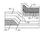
ここで、ドレイン領域(ドレイン電極114と接する半導体層)を拡大したものを図3に示す。図3において、103はゲイト電極、301はチャネル形成領域、302はn+ 層(ソースまたはドレイン電極)、303、304は膜厚の異なるオフセット領域、305はn- 層(LDD領域)である。
【0065】
なお、ここでは説明しないがソース領域(ソース電極113と接する半導体層)も同様の構造を有している。
【0066】
また、図3に示す構造は模式的に記されているが、各領域の膜厚関係には注意が必要である。本願発明を構成するにあたって最も好ましい構成は、膜厚の厚さがn+ 層302<n- 層305<オフセット領域(i層)304の関係にある場合である。
【0067】
なぜならばn+ 層302は電極として機能するだけなので薄くで十分である。一方、n- 層305及びオフセット領域304は電界緩和を効果的に行うために適切な厚さが必要である。
【0068】
本実施例の構成では、チャネル形成領域301からn+ 領域302に至るまでに膜厚の異なる二つのオフセット領域303、304及びLDD領域305が存在する。なお、303はマスク合わせにより形成される膜面方向のオフセット領域であり、マスクオフセット領域と呼ぶ。
【0069】
また、304はi層の膜厚分に相当する膜厚方向のオフセット領域であり、厚さオフセット領域と呼ぶ。厚さオフセット領域304の厚さは100 〜300 nm(代表的には 150〜200nm )の範囲で決定すれば良い。ただし、チャネル形成領域の膜厚よりも膜厚をが厚くする必要がある。チャネル形成領域よりも膜厚が薄いと良好なオフセット効果を望めない。
【0070】
この様なオフセット+LDDからなる構造を本発明者らはHRD(High Resistance Drain )構造と呼び、通常のLDD構造とは区別して考えている。本実施例の場合、HRD構造はマスクオフセット+厚さオフセット+LDDの3段構造で構成されることになる。
【0071】
この時、LDD領域303はLDD領域の膜厚及び不純物濃度によって制御されるため、非常に再現性が高く、特性バラツキが小さいという利点を有する。パターニングによって形成されたLDD領域ではパターニング誤差による特性バラツキが問題となることは従来例で述べた通りである。
【0072】
なお、マスクオフセット領域303の長さ(X1 )はパターニングによって制御されるため、パターニングやガラスの縮み等による誤差の影響を受ける。しかしながら、その後に厚さオフセット領域304とLDD領域305とが存在するので誤差による影響は緩和され、特性バラツキを小さくすることができる。
【0073】
なお、マスクオフセットの長さ(X1 )はチャネル長(L1 )とチャネルエッチング領域の長さ(C1 )を用いて(C1 −L1 )/2で表される。従って、ソース/ドレイン電極形成時のパターニング工程によって所望のオフセット長(X1 )を設定することが可能である。本実施例の構成ではオフセット長(X1 )は 0.3〜3μm(代表的には1〜2μm)とすることができる。
【0074】
なお、図2(D)に示す様な構造の逆スタガ型TFTは、従来の非晶質珪素膜を活性層(島状半導体層)として利用したTFTでは実現できない。なぜならば、非晶質珪素膜を用いる場合、ソース/ドレイン電極とゲイト電極とがオーバーラップする様な構造にしないとキャリア(電子または正孔)の移動度が極めて遅くなってしまうからである。
【0075】
ソース/ドレイン電極とゲイト電極とがオーバーラップする様な構造にしたとしても非晶質珪素膜を用いたTFTのモビリティ(電界効果移動度)はせいぜい1〜10cm2/Vs程度である。それに対して本実施例の様な構造を採用してしまってはモビリティが低すぎてスイッチング素子として機能しない。
【0076】
ところが、本願発明では活性層として結晶性珪素膜を利用しているのでキャリア移動度が十分に速い。従って、本実施例の様な構造としても十分なモビリティを得ることが可能である。即ち、本実施例の構造は半導体層として結晶構造を有する半導体膜を用いたからこそ実現できるのである。
【0077】
また、本実施例の逆スタガ型TFTは、HRD構造を有しているので衝突電離によるホットキャリア注入などの劣化現象に対して非常に強く、高い信頼性を有している。しかも、LDD領域の効果が支配的な上、そのLDD領域が非常に制御性よく形成されているので特性バラツキが非常に小さい。
【0078】
そのため、本実施例の様な構造は高耐圧を必要とし、高い動作速度はそれほど必要としない様な回路を構成するTFTに好適である。
【0079】
また、本実施例の作製工程に示した様に、図2(D)に示した構造の逆スタガ型TFTを得るのに4枚のマスクしか必要としていない。これは従来のチャネルストップ型TFTが6枚マスクを必要としていた事を考えると、スループット及び歩留りが飛躍的に向上することを意味している。
【0080】
以上の様に、本実施例の構成によれば量産性の高い作製工程によって、高い信頼性と再現性を有するボトムゲイト型TFTを作製することが可能である。
【0081】
なお、本実施例の作製工程に従って作製したボトムゲイト型TFT(Nチャネル型TFT)のモビリティは30〜250cm2/Vs (代表的には10〜150cm2/Vs )、しきい値電圧は0〜3Vを実現しうる。
【0082】
〔実施例2〕
本実施例では本願発明の構成において、実施例1とは異なる構成例を示す。TFTの作製工程は基本的には実施例1に従えば良いので、本実施例では必要な部分のみを説明することにする。
【0083】
まず、実施例1の作製工程に従って図5(A)の状態を得る。ここで実施例1と異なる点は、ソース電極501、ドレイン電極502を形成する際にチャネルエッチング領域500の長さをC2 とする点にある。この時、C2 はゲイト電極幅よりも狭く、2〜9μm(代表的には2〜4μm)の範囲で選ばれる。即ち、ゲイト電極とソース/ドレイン電極とがオーバーラップする様に設けることが本実施例の特徴となる。
【0084】
この状態で実施例1に示した様にチャネルエッチング工程を行い、保護膜を設けると図5(B)の状態を得る。この時、503で示される領域がチャネル形成領域となり、そのチャネル長はL2 (=C2 )で表される。また、マスク設計によりオーバーラップさせた領域(マスクオーバーラップ領域と呼ぶ)504の長さ(Y2 )はゲイト電極幅をEとすると、(E−L2 )/2で表される。
【0085】
図5(C)はドレイン領域の拡大図であるが、TFT動作時のキャリアは、チャネル形成領域503(厚さ50nm)、マスクオーバーラップ領域504(厚さ160 nm)、LDD領域505(厚さ50nm)を通ってn+ 層506(厚さ40nm)、ドレイン電極502へと到達する。
【0086】
なお、この場合、マスクオーバーラップ領域504にもゲイト電極からの電界が形成されるが、LDD領域505に近づくにつれて電界は弱まるので、その様な領域は実質的にLDD領域と同様の機能を持つ。勿論、さらにLDD領域505に近づけば完全に電界が形成されなくなり、オフセット(厚さオフセット)領域としても機能しうる。
【0087】
この様に本実施例の構造ではHRD構造が、オーバーラップによる実質的なLDD+厚さオフセット+低濃度不純物によるLDDで構成される。また、オーバーラップ領域504の膜厚が薄い場合には、オーバーラップによる実質的なLDD+低濃度不純物によるLDDのみからなるLDD構造もとりうる。
【0088】
本実施例の構成においても、オーバーラップ領域504、LDD領域505がそれぞれの膜厚で制御されるので非常に特性バラツキが小さい。また、オーバーラップ領域の長さ(Y2 )はパターニング等による誤差を含むが、オーバーラップによるLDD、厚さ方向のオフセット及び低濃度不純物によるLDDはその様な誤差の影響を受けないのでY2 の誤差による特性バラツキは緩和される。
【0089】
なお、本実施例の様な構造はオフセット成分が少なく、高い動作速度を必要とする様な回路を構成するTFTに好適である。
【0090】
また、本実施例の構造では衝突電離によってチャネル形成領域内に蓄積した少数キャリアが速やかにソース電極へと引き抜かれるので基板浮遊効果を起こしにくいという利点を有する。そのため、動作速度が速い上に非常に耐圧特性の高いTFTを実現することが可能である。
【0091】
〔実施例3〕
本実施例では本願発明の構成において、実施例1、2とは異なる構成例を示す。TFTの作製工程は基本的には実施例1に従えば良いので、本実施例では必要な部分のみを説明することにする。
【0092】
まず、実施例1の作製工程に従って図6(A)の状態を得る。ここで実施例1と異なる点は、ソース電極601、ドレイン電極602を形成する際にチャネルエッチング領域600の長さをC3 とする点にある。この時、C3 はゲイト電極幅と一致させるため、1〜10μm(代表的には3〜5μm)となる。
【0093】
この状態で実施例1に示した様にチャネルエッチング工程を行い、保護膜を設けると図6(B)の状態を得る。この時、603で示される領域がチャネル形成領域となり、そのチャネル長はL3 (=C3 )で表される。
【0094】
図6(C)はドレイン領域の拡大図であるが、TFT動作時のキャリアは、チャネル形成領域603(厚さ100 nm)、厚さオフセット領域604(厚さ150 nm)、LDD領域605(厚さ100 nm)を通ってn+ 層606(厚さ50nm)、ドレイン電極602へと到達する。即ち、本実施例の構造ではHRD構造が厚さオフセット+LDDの2段構造で構成される。
【0095】
本実施例の構成においても、厚さオフセット領域604、LDD領域605がそれぞれの膜厚で制御されるので非常に特性バラツキが小さい。また、十分な耐圧特性を得ることが可能である。
【0096】
〔実施例4〕
本実施例では本願発明の構成において、実施例1〜3とは異なる構成例を示す。TFTの作製工程は基本的には実施例1に従えば良いので、本実施例では必要な部分のみを説明することにする。
【0097】
まず、実施例1の作製工程に従って図7(A)の状態を得る。ここで実施例1と異なる点は、ソース電極701、ドレイン電極702を形成する際にソース電極またはドレイン電極のいずれか一方をゲイト電極にオーバーラップさせ、他方はオーバーラップさせない構成とする点にある。
【0098】
なお、本実施例ではチャネルエッチング領域700の長さをC4 とする。この時、C4 は1〜10μm(代表的には3〜6μm)の範囲で選ばれる。
【0099】
この状態で実施例1に示した様にチャネルエッチング工程を行い、保護膜を設けると図7(B)の状態を得る。この時、703で示される領域がチャネル形成領域となり、そのチャネル長はL4 (=C4 −X4 )で表される。
【0100】
ここで、X4 はマスクオフセット領域704の長さである。X4 の数値範囲については実施例1を参考にすれば良い。また、マスクオーバーラップ領域705の長さの数値範囲は実施例2を参考にすれば良い。
【0101】
本実施例は、実施例1で説明したHRD構造と実施例2で説明したHRD構造(またはLDD構造)とを組み合わせた構成である。構造的な説明は実施例1及び実施例2で既に説明したのでここでの説明は省略する。
【0102】
本実施例の様な構造を採用する場合、特にソース領域に実施例2に示したHRD構造(またはLDD構造)を用い、ドレイン領域に実施例1で説明したHRD構造を用いることが好ましい。
【0103】
例えば、ドレイン領域側のチャネル端部(接合部)では特に電界集中が激しく、実施例1に示した様な抵抗成分の多いHRD構造が望ましい。逆に、ソース側ではそこまでの高耐圧対策は必要ないので、実施例2に示した様な抵抗成分の少ないHRD(またはLDD)構造が適している。
【0104】
なお、本実施例において、ソース/ドレイン領域側のいずれか一方に実施例2の構成を組み合わせることも可能である。この様に、実施例1〜3に示したHRD構造またはLDD構造を実施者が適宜選択してソース/ドレイン領域に採用し、回路設計を鑑みて最適な構造を設計すれば良い。この場合、32 =9通りの組み合わせパターンが可能である。
【0105】
〔実施例5〕
本実施例では実施例1〜4に示した構成のボトムゲイト型TFTを用いてCMOS回路(インバータ回路)を構成する場合の例について図8を用いて説明する。なお、CMOS回路は同一基板上に形成されたNチャネル型TFT(NTFTと略記する)とPチャネル型TFT(PTFTと略記する)とを相補的に組み合わせて構成する。
【0106】
図8は実施例4に示した構成を利用したCMOS回路であり、801はPTFTのソース電極、802はNTFTのソース電極、803はN/P共通のドレイン電極である。
【0107】
また、NTFTは実施例1で説明した作製工程によってn+ 層804、805、n- 層806、807が形成されている。一方、PTFTの方にはp++層808、809、p- 層810、811が形成されている。
【0108】
なお、同一基板上にCMOS回路を作製することは非常に容易である。本願発明の場合、まず、実施例1の工程に従って図2(B)の状態を得る。
【0109】
この状態ではN型/P型関係なく15族から選ばれた元素が全面に添加されているが、PTFTを作製する場合にはNTFTとする領域をレジストマスク等で隠して13族から選ばれた元素(代表的にはボロン、インジウムまたはガリウム)を添加すれば良い。
【0110】
本実施例ではボロンを例にとるが、この時、ボロンはリンの濃度の少なくとも3倍以上(代表的には 3×10¹⁹〜 1×10²²atoms/cm3 、好ましくは 3×10²⁰〜 3×10²¹atoms/cm3 )に添加して導電性を反転させなければならない。また、n+ 層及びn- 層全てを完全にp++層及びp- 層に反転させるためには、ボロン添加時の濃度プロファイルを調節してリンの添加深さよりも深く添加することが重要である。
【0111】
従って、ボロンの膜中における濃度プロファイルは図9の様になる。図9において、900は半導体層、901はボロン添加前のリンの濃度プロファイル、902はボロン添加後のボロンの濃度プロファイル、903はp++層、904はp- 層、905はi層である。
【0112】
この時、p++層903の厚さは10〜150 nm(代表的には50〜100 nm)とし、P- 層904の厚さは30〜300 nm(代表的には 100〜200 nm)とする。ただし、PTFTは元来劣化に強いのでp- 層をLDD領域として利用する必要性は必ずしもない。わざわざp- 層904の膜厚について言及したのは、イオン注入法等の添加手段を用いる限り、連続的に変化する濃度勾配によって必ずp- 層が形成されるからである。
【0113】
ところで、本実施例ではNTFTとPTFTのどちらもソース領域側には実施例2に示した構成のHRD構造(オーバーラップ領域を利用したタイプ)を用い、ドレイン領域側には実施例1に示した構成のHRD構造(マスクオフセットを利用したタイプ)を設けている。
【0114】
そのため、上面図で明らかな様にPTFTのソース領域側にはYiの長さを持つオーバーラップ領域を有し、ドレイン領域側にはXiの長さを持つマスクオフセット領域を有している。また、NTFTのソース領域側にはYj の長さを持つオーバーラップ領域を有し、ドレイン領域側にはXj の長さを持つマスクオフセット領域を有している。
【0115】
この時、XiとXj 、YiとYj の長さはそれぞれマスク設計によって自由に調節できる。従って、それぞれの長さは回路構成の必要に応じて適宜決定すれば良く、Nチャネル型とPチャネル型とで揃える必要はない。
【0116】
また、この様な構造ではCMOS回路の共通ドレインとなる領域の耐圧特性を高くすることができるので、動作電圧の高い回路を構成する場合において、非常に有効な構成である。
【0117】
なお、実施例1〜4に示した構成のTFTを用いたCMOS回路の構成を図8に示したが、これ以外の全ての組み合わせも可能であることは言うまでもない。可能な構成パターンとしては、一つのTFTについて9通りあるので、CMOS回路では92 =81通りがある。これらの複数の組み合わせの中から、回路が必要する性能に応じて最適な組み合わせを採用していけば良い。
【0118】
また、本実施例に示した様に本願発明はPTFTにも容易に適用することができる。その場合、本願発明のボトムゲイト型TFT(PTFT)のモビリティは30〜150cm2/Vs (代表的には10〜100cm2/Vs )、しきい値電圧は−1〜−3Vを実現しうる。
【0119】
〔実施例6〕
本実施例では、珪素の結晶化を助長する触媒元素としてGe(ゲルマニウム)を利用した場合の例をついて説明する。Geを利用する場合、汎用性の高さからイオン注入法、イオンドーピング法またはプラズマ処理による添加を行うことが好ましい。また、Geを含む雰囲気中で熱処理を行うことで気相から添加することも可能である。
【0120】
GeはSi(シリコン)と同じ14族に属する元素であるため、Siとの相性が非常に良い。GeとSiとの化合物(Six Ge1-x で示される。ただし0<X<1)は本願発明の半導体層として活用することもできることは既に述べた。
【0121】
そのため、本実施例の様にGeを用いた非晶質珪素膜の結晶化を行った場合、結晶化後に触媒元素をゲッタリングする必要性がない。勿論、ゲッタリング工程を行っても構わないが、TFT特性に影響はない。
【0122】
従って、ゲッタリング工程の加熱処理を省略することができるので製造工程のスループットが大幅に向上する。また、Six Ge1-x 膜を用いたTFTは高いモビリティを示すことが知られているので、珪素膜中におけるGeの含有量が適切であれば動作速度の向上も期待しうる。
【0123】
なお、本実施例の構成は実施例1〜5のいずれの構成に対しても適用することが可能である。
【0124】
〔実施例7〕
本実施例では、本願発明のTFTに対してしきい値電圧を制御するための工夫を施した場合の例について説明する。
【0125】
しきい値電圧を制御するために13族(代表的にはボロン、インジウム、ガリウム)または15族(代表的にはリン、砒素、アンチモン)から選ばれた元素をチャネル形成領域に対して添加する技術はチャネルドープと呼ばれている。
【0126】
本願発明に対してチャネルドープを行うことは有効であり、以下に示す2通りの方法が簡易で良い。
【0127】
まず、非晶質珪素膜を成膜する時点において成膜ガスにしきい値電圧を制御するための不純物を含むガス(例えばジボラン、フォスフィン等)を混在させ、成膜と同時に所定量を含有させる方式がある。この場合、工程数を全く増やす必要がないが、N型及びP型の両TFTに対して同濃度が添加されるため、両者で濃度を異ならせるといった要求には対応できない。
【0128】
次に、図2(D)で説明した様なチャネルエッチング工程(チャネル形成領域の形成工程)が終了した後で、ソース/ドレイン電極をマスクとしてチャネル形成領域(またはチャネル形成領域とマスクオフセット領域)に対して選択的に不純物添加を行う方式がある。
【0129】
添加方法はイオン注入法、イオンドーピング法、プラズマ処理法、気相法(雰囲気からの拡散)、固相法(膜中からの拡散)など様々な方法を用いることができるが、チャネル形成領域が薄いので、気相法や固相法等の様にダメージをあたえない方法が好ましい。
【0130】
なお、イオン注入法等を用いる場合には、TFT全体を覆う保護膜を設けてから行えばチャネル形成領域のダメージを減らすことができる。
【0131】
また、不純物を添加した後はレーザーアニール、ランプアニール、ファーネスアニールまたはそれらを組み合わせて不純物の活性化工程を行う。この時、チャネル形成領域が受けたダメージも殆ど回復する。
【0132】
本実施例を実施する場合、チャネル形成領域には 1×10¹⁵〜 5×10¹⁸atoms/cm3 (代表的には 1×10¹⁵〜 5×10¹⁷atoms/cm3 )の濃度でしきい値電圧を制御するための不純物を添加すれば良い。
【0133】
そして、本実施例を本願発明のTFTに実施した場合、Nチャネル型TFTのしきい値電圧を 0.5〜2.5 Vの範囲に収めることができる。また、Pチャネル型TFTに適用した場合にはしきい値電圧を-0.1〜-2.0Vの範囲に収めることが可能である。
【0134】
なお、本実施例の構成は実施例1〜6のいずれの構成との組み合わせも可能である。また、実施例5のCMOS回路に適用する場合、N型TFTとP型TFTとで添加濃度や添加する不純物の種類を異なるものとすることもできる。
【0135】
〔実施例8〕
図2(D)に示した構造では、島状半導体層を完全に囲む様にしてソース電極113とドレイン電極114とが形成されている。本実施例ではこれとは別の構成について説明する。
【0136】
図10(A)に示す構造は、基本的には図2(D)と似ているが、ソース電極11及びドレイン電極12の形状が異なる点に特徴がある。即ち、一部において島状半導体層(厳密にはソース/ドレイン領域)よりもaで示される距離だけ内側にソース電極11及びドレイン電極12が形成されている。
【0137】
また、13で示される領域は、チャネル形成領域14と同じ膜厚を有する領域であり、距離aの幅を持つ。図面上では模式的に表しているが、距離aは1〜300 μm(代表的には10〜200 μm)である。
【0138】
ここで作製工程と照らし合わせて本実施例の特徴を説明する。本実施例では図10(B)に示す様にソース電極11及びドレイン電極12を形成する。ここで15は島状半導体層であり、端部16が露出する。
【0139】
この状態でチャネルエッチング工程を行うと、ソース電極11及びドレイン電極12がマスクとなって自己整合的に島状半導体層15がエッチングされる。この場合、端部16も同時にエッチングされる。
【0140】
この様にして図10(A)の様な構造が得られる。従って、端部16がチャネル形成領域14と同じ膜厚を有することは明らかである。
【0141】
この島状半導体層の突出部13を形成する理由は以下の2つがある。
(1)チャネルエッチング工程におけるエッチングモニタとして利用する。
(2)後工程で保護膜や層間絶縁膜を形成する際に、島状半導体層の段差によるカバレッジ不良を低減する。
【0142】
エッチングモニタとしては、製造過程における抜き取り検査によってチャネル形成領域が適切な膜厚となっているかどうかを検査する場合に用いる。
【0143】
なお、本実施例の構成は実施例1〜7のいずれの構成とも組み合わせることが可能である。
【0144】
〔実施例9〕
本実施例では実施例5に示したCMOS回路(インバータ回路)の回路構成の例について図11を用いて説明する。
【0145】
図11(A)に示すのは、図8に示したものと同一構造のCMOS回路である。この場合、回路構成はゲイト電極20、N型TFTの半導体層21、P型TFTの半導体層22、N型TFTのソース電極23、P型TFTのソース電極24、共通ドレイン電極25から構成される。
【0146】
なお、各端子部a、b、c、dはそれぞれ図11(C)に示したインバータ回路の端子部a、b、c、dに対応している。
【0147】
次に、図11(B)に示すのは、N型TFTとP型TFTとでドレイン領域となる半導体層を共通化した場合の例である。各符号は図11(A)で説明した符号に対応している。
【0148】
図11(B)の構造ではTFT同士を非常に高い密度で形成することができるため、回路を高集積化する場合などに非常に有効である。共通化した半導体層はPN接合を形成するが問題とはならない。
【0149】
〔実施例10〕
本実施例では、実施例1〜5の構成のTFT及びCMOS回路を作製する過程において、加熱処理の手段としてランプアニールを用いる場合の例を示す。
【0150】
ランプアニールとしてはRTA(Rapid Thermal Anneal)による熱処理が知られている。これは赤外ランプからの強光を照射することにより短時間(数秒から数十秒)で高温の加熱処理を行う技術であり、スループットが非常に良い。また、赤外光以外に補助的に紫外光を用いる場合もある。
【0151】
本願発明においては、非晶質半導体膜の結晶化工程、結晶性半導体膜の結晶性改善工程、触媒元素のゲッタリング工程、しきい値制御のための不純物の活性化工程等に加熱処理を行う。この様な時に本実施例を利用することができる。
【0152】
なお、本実施例の構成と他の実施例の構成とは自由に組み合わせることが可能である。
【0153】
〔実施例11〕
本実施例では実施例1とは異なる手段で触媒元素のゲッタリングを行う場合について説明する。
【0154】
実施例1では15族から選ばれた元素のみを利用してゲッタリング工程を行っているが、触媒元素のゲッタリング工程は13族及び15族から選ばれた元素が添加された状態でも実施することができる。
【0155】
その場合、まず図1(E)に示す状態を得たら、Nチャネル型TFTとなる領域のみをレジストマスクで隠して次にボロンを添加する。即ち、Nチャネル型TFTとなる領域にはリンのみが存在し、Pチャネル型TFTとなる領域にはボロンのみが存在する。
【0156】
そして、その状態で加熱処理を行い、触媒元素のゲッタリング工程を実施すれば良い。本発明者らの実験ではリンのみによるゲッタリング効果よりもリン+ボロンによるゲッタリング効果の方が効果が高いことが確かめられている。ただし、ボロンのみではゲッタリング効果はなく、リン+リンよりも高濃度のボロンという組み合わせの時に高いゲッタリング効果を示した。
【0157】
なお、本実施例の構成と他の実施例の構成とは自由に組み合わせることが可能である。
【0158】
〔実施例12〕
基板として耐熱性の高い石英基板やシリコン基板を用いている場合、n+ 導電層及びn- 導電層を形成する前にハロゲン元素を含む酸化性雰囲気中で700 〜1100℃程度の加熱処理を行うことも有効である。これはハロゲン元素による金属元素のゲッタリング効果を利用する技術である。
【0159】
また、この技術と実施例11に示した様なゲッタリング工程とを併用することでさらに徹底的に非晶質半導体膜の結晶化に利用した触媒元素を除去することができる。こうして、触媒元素を少なくともチャネル形成領域から徹底的に除去しておけば信頼性の高い半導体装置を得ることができる。
【0160】
〔実施例13〕
本実施例では、実施例1で説明した基本的な作製工程に従って、同一基板上にドライバー回路(周辺駆動回路)と画素マトリクス回路とを一体形成したアクティブマトリクス型表示装置を作製する例を示す。
【0161】
本実施例ではドライバー回路としては基本構成であるCMOS回路(図11(B)に示したタイプ)を示す。なお、ドライバー回路以外に、D/Aコンバータ回路、メモリ回路、γ補正回路などの信号処理回路(これらをドライバー回路と区別するためにロジック回路と呼ぶ)を本願発明のTFTで構成することも可能である。その場合にもCMOS回路が基本回路として用いられる。
【0162】
また、画素マトリクス回路としてはマルチゲイト型TFTを用いる例を示す。本実施例ではダブルゲイト構造とする例を示すが、シングルゲイト構造でもトリプルゲイト構造でも構わない。
【0163】
まず、実施例1の作製工程を利用して図2(A)に示す工程(触媒元素のゲッタリング工程)までを終了する。この状態を図12(A)に示す。
【0164】
図12(A)において、30はガラス基板、31は下地膜、32はCMOS回路となるPTFTのゲイト電極、33はNTFTのゲイト電極である。また、34、35は画素TFTのゲイト電極であり、図示されない部分で両電極は接続されている。なお、本実施例ではゲイト電極の材料としてタンタル(Ta)と窒化タンタル(TaN)からなる積層膜を用いる。場合によってはゲイト電極表面にTa2 O5 で示される陽極酸化膜を設けてもよい。また、タンタル膜単体でゲイト電極を構成しても良い。
【0165】
また、その上には窒化珪素膜36、酸化窒化珪素膜37が設けられ、さらにその上に半導体層が形成される。本実施例の半導体層は実施例1に示した様な手段で結晶化され、その後、リン添加工程が行われてn+ 層38、n- 層39、i層40が形成される。これら各層の詳細な条件は実施例1に示してある。
【0166】
次に、RTA処理によるゲッタリング工程を行い、i層40の中に含まれる触媒元素(実施例1に従えばニッケル)をリンを含む領域に対してゲッタリングさせる。
【0167】
次に、CMOS回路のPTFTとなる領域以外をレジストマスク(図示せず)で隠して13族から選ばれた元素であるボロンを添加する。本実施例では先程添加したリン濃度の3倍の濃度のボロンを添加して、P++層41、P- 層42を形成する。(図12(B))
【0168】
次に、レーザーアニール工程を行い、イオン注入工程(またはイオンドーピング工程)で非晶質化した結晶性半導体層の結晶性を改善する。また、同時に添加した不純物(リン及びボロン)の活性化も行われる。(図12(C))
【0169】
なお、このレーザーアニール工程の前に、RTA処理による脱水素化を行っておくとレーザーアニールの際に水素の突沸現象を防ぐことができる。
【0170】
次に、結晶性半導体層をエッチングして島状半導体層43、44を形成する。なお、この時、次に形成する電極(第2配線)とゲイト配線との一部を接続するためにコンタクトホールを形成する。
【0171】
なお、前述のレーザーアニール工程は結晶性半導体層を島状半導体層に加工してから行うことも可能である。
【0172】
そして、導電性を有する薄膜を形成してパターニングを行い、CMOS回路のソース電極45(NTFT)、46(PTFT)、共通ドレイン電極47を形成する。また、画素TFTのソース電極48、ドレイン電極49を形成する。なお、50で示される電極は、マスクとしてのみ機能するため、本明細書中ではマスク電極と呼ぶことにする。(図13(A))
【0173】
図13(A)の状態が得られたら、チャネルエッチング工程を行ってチャネル形成領域51〜54を形成する。この時、ドライバー回路の方はどちらのTFTもドレイン側のみにマスクオフセット領域を設けて、両方のソース側にオーバーラップ領域を設けた構成とする。
【0174】
また、画素TFTは図13(B)に示す様にソース電極48及びドレイン電極49と接続する方にマスクオフセット領域を設け、マスク電極50の下にはオーバーラップ領域を設けた構成とする。
【0175】
画素TFTはソース/ドレイン領域が映像信号の充放電の際に入れ替わるので、TFT両端の耐圧を高くする必要がある。また、マスク電極50の下方の抵抗成分が高いとスイッチング動作が遅くなるので、オーバーラップ領域を設けてキャリアが移動しやすい状態にすることが望ましい。
【0176】
なお、本実施例は最も好ましいと思われる一実施例であり、本実施例がこの構造に限定されることはない。実施者は、実施例1〜4で説明したそれぞれの構造の長所を生かして最適な構造を選択すれば良い。
【0177】
次に、酸化窒化珪素膜でなる保護膜55を200 nmの厚さに形成して、その上に有機性樹脂膜でなる層間絶縁膜56を形成する。有機性樹脂膜56としてはポリイミド、ポリアミド、ポリイミドアミド、アクリルを用いることができる。
【0178】
次に、層間絶縁膜56に対してコンタクトホールを形成して、透明導電膜(代表的にはITO)から構成される画素電極57を形成する。最後に水素化を行って図13(C)に示す様なアクティブマトリクス基板が完成する。
【0179】
後は、公知のセル組み工程を利用して対向基板とアクティブマトリクス基板との間に液晶層を挟持すればアクティブマトリクス型液晶表示装置を作製することが可能である。
【0180】
なお、本実施例に示したアクティブマトリクス基板を作製するに必要なパターニング回数は7回である。その工程を以下に示す。
(1)ゲイト電極パターニング
(2)ボロン添加領域パターニング
(3)島状半導体層パターニング
(4)ゲイトコンタクトパターニング
(5)ソース/ドレイン電極パターニング
(6)ITOコンタクトパターニング
(7)ITOパターニング
【0181】
以上の様に、非常に少ないマスク数でアクティブマトリクス基板を作製することができるため、スループットが大幅に向上する。また、同時に実施例1〜5に示した構成のTFTを用いて自由に回路設計することができるにので、信頼性と再現性の高い表示装置を容易に実現することができる。
【0182】
なお、本実施例に示した画素マトリクス回路の一部を上面から見た図を図14(A)に示す。なお、図14(A)では基本的に本実施例で用いた符号を付してある。従って必要箇所のみを説明することとする。
【0183】
図14(A)に示す図をA−A’で切断した断面図が図14(B)である。図13(C)では図示しなかったが、図14(B)に示す様にゲイト配線と平行に容量配線58が形成されている。
【0184】
この容量配線58はドレイン電極50と重畳する領域(点線で囲まれた領域)において補助容量(Cs)を形成する。この時、補助容量の誘電体はゲイト絶縁層が担う。なお、補助容量の構造は本実施例に限定されるものではない。
【0185】
〔実施例14〕
本実施例では、実施例13に示した工程とは異なる構成でアクティブマトリクス型表示装置を作製する場合の例を示す。
【0186】
本実施例の特徴は、まず、触媒元素を利用した結晶化の後、レーザーアニールによる結晶性の改善工程を行わない点にある。即ち、結晶化後はそのままリンの添加工程、触媒元素のゲッタリング工程等を実施例13と同様に行う。
【0187】
そして、本実施例の特徴はチャネル形成領域の結晶性改善工程(不純物の活性化、再結晶化等)を図15に示す様に保護膜55を設けた後で行う点にある。即ち、レーザー光は酸化窒化珪素膜でなる保護膜55を介して照射され、自己整合的にチャネル形成領域51〜54に対して行われる。
【0188】
この様に図15の状態でレーザーアニールを行うと、ソース/ドレイン領域からのリンやボロンといった不純物の逆拡散(Out Diffusion )を抑えることができる。また、レーザー光のパワー(レーザーエネルギー)も半分位で済むという利点を得ることができる。
【0189】
なお、本実施例は図面に示された構造に限定されることはない。実施者は、実施例1〜4で説明したそれぞれのTFT構造の長所を生かして最適な構造を選択して回路設計を行えば良い。また、本実施例は他の全ての実施例に示される構成との組み合わせが可能である。
【0190】
〔実施例15〕
本実施例では、実施例13において、結晶化後のレーザーアニール工程を省略した場合の例を示す。本実施例の場合、結晶化工程後はイオンドーピング法を用いてリンを添加して、RTAにより触媒元素のゲッタリング工程を行う。
【0191】
そして、次にイオンドーピング法によりボロンを添加してPTFTとなる半導体層上にp++層41、p- 層42を形成する。なお、38、39はそれぞれn+ 層とn- 層である。
【0192】
この状態でRTAによるアニール工程を行う。本実施例ではRTAによるアニール処理によって添加された不純物(リン及びボロン)の活性化と半導体層の脱水素化(質量分離をしないイオンドーピングではリンやボロンと一緒に水素も打ち込まれてしまうため)を行っている。(図16(A))
【0193】
次に、レーザーアニール工程を行い、不純物の添加工程で非晶質化した半導体層を再結晶化させ、結晶性を改善する。なお、このレーザーアニール工程は半導体層をエッチングして島状半導体層に加工してから行っても良い。
【0194】
後の工程は実施例13に従えば良い。なお、本実施例は図面に示された構造に限定されることはない。実施者は、実施例1〜4で説明したそれぞれのTFT構造の長所を生かして最適な構造を選択して回路設計を行えば良い。また、本実施例は他の全ての実施例に示される構成との組み合わせが可能である。
【0195】
〔実施例16〕
本実施例は実施例13〜15とは異なる構成を用いてアクティブマトリクス基板を作製する場合の例を示す。
【0196】
まず、実施例1の工程に従って形成した結晶性半導体層に対してリンの添加工程を行う。こうしてn+ 層38、n- 層39、i層40を形成する。こうして図17(A)の状態を得たら、次に、PTFTとなる領域に対してボロンの添加工程を行い、p++層41、p- 層42を形成する。(図17(B))
【0197】
次に、RTAによるアニールを行い、触媒元素(本実施例ではニッケル)のゲッタリング工程を行う。本実施例の特徴は、NTFTではリンによるゲッタリング効果が得られ、PTFTではリン+ボロンによるゲッタリング効果が得られる点にある。(図17(C))
【0198】
こうして図17(C)の状態が得られたら、レーザーアニール工程を行い、不純物添加によって非晶質化した半導体層の結晶性を改善する。なお、図17(B)に示すRTAによるゲッタリング工程が半導体層の脱水素化も兼ねている。そのため、不純物添加により膜中に多量の水素が存在したとしても水素の突沸現象は生じない。
【0199】
なお、このレーザーアニールによる再結晶化工程は半導体層をエッチングして島状半導体層に加工してから行っても良い。
【0200】
後の工程は実施例13に従えば良い。なお、本実施例は図面に示された構造に限定されることはない。実施者は、実施例1〜4で説明したそれぞれのTFT構造の長所を生かして最適な構造を選択して回路設計を行えば良い。また、本実施例は他の全ての実施例に示される構成との組み合わせが可能である。
【0201】
〔実施例17〕
本実施例では実施例13に示した作製工程を基本として、反射型液晶表示装置を作製する場合の例を示す。ここで反射型液晶表示装置の画素マトリクス回路の任意の画素の上面図を図18(A)に示す。
【0202】
なお、実施例13で説明した部分と同じところは同一の符号を付して表し、詳細な説明は省略する。また、図14(A)をB−B’で切断した断面図を図18(B)に示す。
【0203】
まず、実施例13と異なる点は容量配線59が画素内全面に広がっている点である。反射型は実施例13に示した様な透過型と違って、開口率を高くするという要求がないため、画素電極61の裏側は全て自由に使えるのである。
【0204】
また、本実施例の場合、ドレイン電極60をも画素内全面に広げ、可能な限り広い範囲で容量配線59と重畳する様に配置する。こうすることで画素内の殆どを補助容量として利用することができ、大容量を確保することができる。
【0205】
また、画素電極61は反射性電極であり、反射率の高いアルミニウムまたはアルミニウムを主成分とする材料を用いるのが好ましい。また、本実施例の液晶表示装置を投影型表示装置に利用するなら画素電極表面は平坦であることが好ましい。逆に直視型表示装置に用いるなら表面に凹凸をつけて乱反射率を増すなどして視野角を広げる工夫が必要である。
【0206】
なお、本実施例は図面に示された構造に限定されることはない。実施者は、実施例1〜4で説明したそれぞれのTFT構造の長所を生かして最適な構造を選択して回路設計を行えば良い。また、本実施例は他の全ての実施例に示される構成との組み合わせが可能である。
【0207】
〔実施例18〕
本実施例では、実施例13に示した液晶表示装置におけるBM(ブラックマトリクス)の構成に関する説明を行う。
【0208】
まず、実施例13の作製工程に従って層間絶縁膜56の形成までを行う。本実施例では層間絶縁膜56として感光性を有するアクリル樹脂を用いる。そして、層間絶縁膜56をパターニングした後、ハーフエッチングして凹部65、66を形成する。(図19(A))
【0209】
図19(A)の状態を得たら、黒色樹脂(図示せず)を全面に形成する。黒色樹脂としてはグラファイト、カーボン、色素等を含んだ有機性樹脂膜を用いることができる。有機性樹脂膜はポリイミドやアクリル等が用いられる。本実施例ではグラファイトを分散させた感光性アクリル樹脂を利用する。
【0210】
こうして黒色樹脂を形成したら、凹部65、66を形成した領域のみを選択的に露光して、その部分のみに黒色樹脂を残すことが可能である。その後、酸素プラズマ雰囲気でアッシングを行い、平坦性を高めることも有効である。
【0211】
こうして黒色樹脂からなるブラックマトリクス67、68を形成したら、次にITO膜で構成される画素電極69を形成する。本実施例では画素電極69の端部とブラックマトリクス68の端部とが重畳する(画素電極の端面がBMより内側にある)様に画素電極69をパターニングする。
【0212】
以上の様にして図19(B)に示す様な構造のアクティブマトリクス基板が完成する。後は公知のセル組み工程を行えば、液晶表示装置を作製することが可能である。本実施例の様なブラックマトリクスは他の配線との間で寄生容量を形成しないという利点がある。
【0213】
なお、本実施例は図面に示された構造に限定されることはない。実施者は、実施例1〜4で説明したそれぞれのTFT構造の長所を生かして最適な構造を選択して回路設計を行えば良い。また、本実施例は他の全ての実施例に示される構成との組み合わせが可能である。
【0214】
〔実施例19〕
本実施例では実施例18とは異なるブラックマトリクスを用いた場合の例について説明する。具体的にはブラックマトリクスとして、導電性膜を用いる場合の例を示す。
【0215】
図20において、56は有機性樹脂膜からなる層間絶縁膜、71〜74は導電性膜からなるブラックマトリクスまたはブラックマトリクスを兼ねる配線パターンである。導電性膜としては、チタン膜、クロム膜、チタンとアルミニウムの積層膜などを用いることができる。
【0216】
また、本実施例のブラックマトリクスは導電性であるため、ブラックマトリクスとしての役割以外に様々な活用方法がある。まず、71で示されるパターンはコモン電位(接地電位)に固定されたブラックマトリクスである。また、72で示されるパターンはCMOS回路のドレイン電極と接続し、取り出し配線として利用される。この様に本実施例を用いれば多層配線構造が容易に実現できる。
【0217】
また、73で示されるパターンはCNMOS回路のソース電極と接続しており、接続配線として機能とブラックマトリクスとしての機能とを有している。また、74で示されるパターンは画素マトリクス回路に配置されるブラックマトリクスであり、基本的に配線やTFT上に設けられる。
【0218】
そして、ブラックマトリクス(またはブラックマトリクスを兼ねる配線)71〜74の上には再び層間絶縁膜75が設けられる。この層間絶縁膜75は酸化珪素膜、窒化珪素膜、酸化窒化珪素膜、有機性樹脂膜またはそれらの積層膜で構成される。この層間絶縁膜75は後に補助容量の誘電体として機能する。
【0219】
こうして層間絶縁膜75を形成したら、コンタクトホールを形成してITOでなる画素電極76を形成する。なお、画素マトリクス回路内ではブラックマトリクス74と画素電極76との間で補助容量77が形成される。
【0220】
ここで画素マトリクス回路のブラックマトリクスの配置例を図21に示す。図21は図14(A)に示される構造に対してブラックマトリクス78を重ね合わせた場合の配置例である。なお、79で示される太線が画素電極、80は画素電極79と下方のドレイン電極とのコンタクト部である。
【0221】
ブラックマトリクス78は基本的に配線やTFT上を覆い、映像表示領域81やコンタクト部80にのみ開口窓を有する。本実施例の様な透過型液晶表示装置においては、ブラックマトリクスの占有面積を減らし、映像表示領域81の面積を広げる(開口率を向上する)ことが最重要課題となる。
【0222】
なお、本実施例は図面に示された構造に限定されることはない。実施者は、実施例1〜4で説明したそれぞれのTFT構造の長所を生かして最適な構造を選択して回路設計を行えば良い。また、本実施例は他の全ての実施例に示される構成との組み合わせが可能である。
【0223】
〔実施例20〕
本実施例では、実施例13に示した構造とは異なるTFT構造でアクティブマトリクス基板を作製した場合の例を説明する。
【0224】
図22に示す構造において最も重要な点は、各半導体層(ソース/ドレイン領域)の最上部は第1の導電層(n+ 領域またはp++領域)であり、各導電層は一旦保護膜55及び層間絶縁膜56で覆われ、その上で取り出し電極81〜85が電気的に接続している点にある。
【0225】
この様な構造とする場合、チャネル形成領域を形成する際のチャネルエッチング工程はレジストマスクを用いて行うことになる。その上で保護膜55と層間絶縁膜56を形成して、取り出し電極87〜91を形成する。
【0226】
本実施例の構造の様に、各取り出し電極(ソース/ドレイン電極又は引回し配線として機能する)87〜91を層間絶縁膜56によってゲイト電極から引き離すことでソース/ドレイン電極とゲイト電極との間の寄生容量をさらに低減することが可能である。層間絶縁膜56として、比誘電率の小さい有機性樹脂材料を用いればさらに効果的である。
【0227】
なお、本実施例の構成は、実施例1〜4で示したTFTに対しても適用することが可能であり、無論、他の全ての実施例と組み合わせることが可能である。また、本実施例は図面に示された構造に限定されることはない。実施者は、実施例1〜4で説明したそれぞれのTFT構造の長所を生かして最適な構造を選択して回路設計を行えば良い。
【0228】
〔実施例21〕
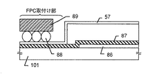
本実施例では、実施例13〜21に示した構成のアクティブマトリクス基板において、外部端子との接続構造に関する説明を行う。なお、図23に示す図は外部端子(代表的にはフレキシブルプリントサーキット(FPC))と接続する端子部(以下、FPC取付け部と呼ぶ)の拡大図であってアクティブマトリクス基板の端部に位置する。
【0229】
また、図23おいて、101はガラス基板、86は絶縁層であり、実際には図1(A)に示される下地膜102、窒化珪素膜104及び酸化窒化珪素膜105との積層構造で構成される。また、その上には第2の配線層87が形成されている。この第2の配線層87は外部端子からの信号をソース/ドレイン電極やゲイト電極等へ伝達するための接続配線層である。
【0230】
本実施例の特徴は、まず、第2の配線層87が直接ガラス基板101に接している点である。この構造を実現するためには、実施例1で説明した3回目のパターニング工程において、図23に示されるFPC取付け部に存在する絶縁層86を完全に取り除く必要がある。第2の配線層87の下地を固いガラス基板としておくとFPCをしっかりと圧着することができる。
【0231】
また、FPC取付け部においては、その後の工程で層間絶縁膜56も部分的に除去し、その上のITO膜57が第2の配線層86と接触する様な構造とする。このITO膜57は少なくともFPC取付け部で第2の配線層86上に積層されていれば良く、場合によっては電極パッドとしてFPC取付け部のみに独立のパターンとして形成しても良い。
【0232】
このITO膜57は後に異方性導電膜88を形成した際に異方性導電膜中に含まれる導電性粒子(金コーティングしたシリカガラスなど)がITO膜にめり込みオーミック接触を良好なものとするためのバッファ層として機能する。
【0233】
そして、FPC取付け部を図23の様な構造としたら、異方性導電膜88を用いてFPC端子89を圧着する。こうして図23に示す様な接続構造を実現することができる。この様な接続構造を実施例13〜20に示したアクティブマトリクス基板に適用すると外部端子との良好な電気接続が可能となる。
【0234】
〔実施例22〕
本実施例では、大型ガラス基板上に本願発明のTFTを形成するにあたってパターニングの効率を改善するための工夫について説明する。
【0235】
大型ガラス基板上に微細な半導体回路を作製する場合、ガラス基板の反りや縮みによるパターニング誤差が問題となる。そのため、ステッパーと呼ばれる露光装置を用いた露光法が注目されている。ステッパー露光では、1枚のレチクル内のある一部のみを部分的に露光することが可能である。
【0236】
本実施例の場合、1枚のレチクルに対してドライバー回路、画素マトリクス回路といった必要な回路パターンを部分毎に形成する。また、この時、同一構造の繰り返しとなる領域は同一回路パターンの繰り返し露光で形成する。
【0237】
図24において、A、C、G、Iパターンはドライバー回路の端部を作製するための回路パターンである。また、B、Hパターンは水平走査用ドライバー回路の繰り返し回路パターン、D、Fパターンは垂直走査用ドライバー回路の繰り返し回路パターンである。また、Eパターンは画素マトリクス回路の繰り返し回路パターンである。
【0238】
この様に、同一構造の回路が連続的に接続して構成される様なドライバー回路や画素マトリクス回路は、端部のみは専用の回路パターンで形成して、内部は完全に同一回路パターンを繰り返し利用して全体のパターン形成を行う。
【0239】
この方式を用いると、回路パターンを共用できるため、1枚のレチクルに書き込む回路パターンが少なくなり、レチクルの縮小化が図れる。また、1枚のレチクルを使い回すことで、どの様な大型基板に対しても対応できるので、マスクチェンジする時間が省かれ、スループットが向上する。
【0240】
なお、例えば画素マトリクス回路がSXGAである場合、行方向には1280画素が並び、列方向には1024画素が並ぶ。従って、前述のEパターンの行方向に256 個分の画素に相当するパターン回路を書き込んでおけば、行方向は5回の繰り返し露光で終了する。また、列方向に256 個分の画素に相当するパターン回路を書き込んでおけば、列方向は4回の繰り返し露光で終了する。
【0241】
この様に、行方向及び列方向の繰り返し露光回数をそれぞれn、mとし、行方向及び列方向の画素数をそれぞれX、Yとすると、画素マトリクス回路を形成するための回路パターン内には行方向にX/n、列方向にY/mの画素パターンを書き込んでおく必要がある。この規則性を利用すれば、ATV(アドバンストTV)の様な1920×1080画素といった高精細なディスプレイも容易に実現することができる。
【0242】
〔実施例23〕
本実施例では実施例13〜20に示した構成のアクティブマトリクス基板を用いてAMLCD(アクティブマトリクス型液晶表示装置)を構成した場合の例について説明する。なお、本実施例のAMLCDは駆動回路及び画素マトリクス回路を同一基板上に作製された逆スタガ型TFTで構成している。また、駆動回路はCMOS回路を基本として回路構成がなされているので消費電力が低い。
【0243】
ここで本実施例のAMLCDの外観を図25に示す。図25(A)において、1101はアクティブマトリクス基板であり、その上には本願発明のTFTによって画素マトリクス回路1102、ソース側駆動回路1103、ゲイト側駆動回路1104が構成されている。また、1105は対向基板である。
【0244】
本実施例のAMLCDはアクティブマトリクス基板1101と対向基板1105とが端面を揃えて貼り合わされている。ただし、ある一部だけは対向基板1105を取り除き、露出したアクティブマトリクス基板に対してFPC(フレキシブル・プリント・サーキット)1106を接続してある。このFPC1106によって外部信号を回路内部へと伝達する。
【0245】
また、FPC1106を取り付ける面を利用してICチップ1107、1108が取り付けられている。これらのICチップはビデオ信号の処理回路、タイミングパルス発生回路、γ補正回路、メモリ回路、演算回路など、様々な回路をシリコン基板上に形成して構成される。図8では2個取り付けられているが、1個でも良いし、さらに複数個であっても良い。
【0246】
また、図25(B)の様な構成もとりうる。図25(B)において図25(A)と同一の部分は同じ符号を付してある。ここでは図25(A)でICチップが行っていた信号処理を、同一基板上にTFTでもって形成されたロジック回路1109によって行う例を示している。
【0247】
この場合、ロジック回路1109も駆動回路1103、1104と同様にCMOS回路を基本として構成され、本願発明を利用した逆スタガ型TFTで作製することが可能である。
【0248】
また、本願発明を利用したTFTはAMLCDのスイッチング素子として以外にも、EL(エレクトロルミネッセンス)表示装置のスイッチング素子として利用することも可能である。また、イメージセンサ等の回路を本願発明のボトムゲイト型TFTで構成することもできる。
【0249】
以上の様に、本願発明を利用したTFTでもって様々な電気光学装置を作製することが可能である。なお、本明細書中において電気光学装置とは、電気的信号を光学的信号に変換する装置またはその逆を行う装置と定義する。
【0250】
また、本実施例のAMLCDを作製するにあたってブラックマトリクスは対向基板側に設けても良いし、アクティブマトリクス基板に設ける構成(BM on TFT)としても良い。
【0251】
また、カラーフィルターを用いてカラー表示を行っても良いし、ECB(電界制御複屈折)モード、GH(ゲストホスト)モードなどで液晶を駆動し、カラーフィルターを用いない構成としても良い。
【0252】
また、特開昭8-15686 号公報に記載された技術の様に、マイクロレンズアレイを用いる構成にしても良い。
【0253】
〔実施例24〕
実施例23に示したAMLCDは、様々な電子機器のディスプレイとして利用される。なお、本実施例に挙げる電子機器とは、AMLCDに代表される電気光学装置を搭載した製品と定義する。
【0254】
その様な電子機器としては、ビデオカメラ、スチルカメラ、プロジェクター、プロジェクションTV、ヘッドマウントディスプレイ、カーナビゲーション、パーソナルコンピュータ(ノート型を含む)、携帯情報端末(モバイルコンピュータ、携帯電話等)などが挙げられる。それらの一例を図26に示す。
【0255】
図26(A)は携帯電話であり、本体2001、音声出力部2002、音声入力部2003、表示装置2004、操作スイッチ2005、アンテナ2006で構成される。本願発明は表示装置2004等に適用することができる。
【0256】
図26(B)はビデオカメラであり、本体2101、表示装置2102、音声入力部2103、操作スイッチ2104、バッテリー2105、受像部2106で構成される。本願発明は表示装置2102に適用することができる。
【0257】
図26(C)はモバイルコンピュータ(モービルコンピュータ)であり、本体2201、カメラ部2202、受像部2203、操作スイッチ2204、表示装置2205で構成される。本願発明は表示装置2205等に適用できる。
【0258】
図26(D)はヘッドマウントディスプレイであり、本体2301、表示装置2302、バンド部2303で構成される。本発明は表示装置2302に適用することができる。
【0259】
図26(E)はリア型プロジェクターであり、本体2401、光源2402、表示装置2403、偏光ビームスプリッタ2404、リフレクター2405、2406、スクリーン2407で構成される。本発明は表示装置2403に適用することができる。
【0260】
図26(F)はフロント型プロジェクターであり、本体2501、光源2502、表示装置2503、光学系2504、スクリーン2505で構成される。本発明は表示装置2503に適用することができる。
【0261】
以上の様に、本願発明の適用範囲は極めて広く、あらゆる分野の電子機器に適用することが可能である。また、他にも電光掲示盤、宣伝公告用ディスプレイなどにも活用することができる。
【0262】
〔実施例25〕
本実施例では、本願発明の逆スタガ型TFTを用いて構成した回路の構成例について説明する。ここではまず、シフトレジスタ回路を構成した場合の例について図27を用いて説明する。なお、本実施例では実施例13に示した構成の層構造を採用している。
【0263】
また、図27(A)はシフトレジスタ回路の任意の1段のみを取り出した回路パターンであり、図27(B)はその等価回路図である。本実施例では図27(A)と図27(B)との位置関係が概ね対応しているので、図27(A)の説明において、必要に応じて図27(B)の符号を参照する。
【0264】
図27(A)において、TFT(a)〜TFT(d)及びTFT(g)〜TFT(j)で構成される回路はクロックドインバータ回路、TFT(e)、TFT(g)で構成される回路はインバータ回路である。なお、TFT(e)はダブルゲイト構造のTFTを用いている。
【0265】
また、1201はCLK線(クロック信号線)、1202は反転CLK線(反転クロック信号線)、1203はGND配線(グランド線)、1204はVdd線(電源線)である。これらの左上がりの斜線模様で示される配線は全て第2の配線層(図13(A)の45〜50で示される)である。
【0266】
また、例えば1205で示される配線はTFT(a)のゲイト電極として機能する。この様に、右上がりの斜線模様で示される配線層は全て第1の配線層(図12(A)の32〜35で示される)であり、これら第1の配線層と半導体層とが重なる部分を特にゲイト電極と呼ぶ。
【0267】
本実施例では、TFTのソース側にはオーバーラップ領域(図中、ovと示す)を設けた構成とし、ドレイン側にはマスクオフセット領域(図中、ofと示す)を設けた構成としている。従って、図27(B)においてTFT(a)〜(d)で構成されるクロックドインバータ回路を例にとると、上から順にov/of/ov/of/of/ov/of/ovとなる。
【0268】
即ち、TFT(a)と(b)の部分では実施例13で説明した画素TFTのダブルゲイト構造とほぼ同じ構成となっているため、ov/of/ov/ofの様に繰り返される。また、TFT(b)と(c)の部分ではNTFTとPTFTとでドレイン電極を共通化したCMOS構造を構成しているので、実施例5で説明した様にov/of/of/ovの様な構成となる。
【0269】
他の回路も基本的には同様であり、TFT(e)はダブルゲイト構造であるのでGND線1203と接続する側から順に、ov/of/ov/ofの様な構成となる様に各TFT構造が決定されている。
【0270】
以上の様な構成によって、動作速度を落とすことなく耐圧特性を高めた信頼性の高い半導体回路を構成することができる。また、その様な半導体回路を用いることで電気光学装置の信頼性を高めることが可能である。
【0271】
〔実施例26〕
本実施例では、本願発明の逆スタガ型TFTを用いて構成した回路の構成例について説明する。ここではまず、バッファ回路(図面左)及びアナログスイッチ回路(図面右)を構成した場合の例について図28を用いて説明する。なお、本実施例では実施例20に示した構成の層構造を採用している。また、図28(A)は回路パターンであり、図28(B)はその等価回路図である。
【0272】
図28(A)の回路パターンにおいて、TFT(a’)〜(h’)が本願発明を利用したTFTであり、TFT(a’)、(b’)及びTFT(c’)、(d’)でそれぞれ一つのバッファ回路を構成している。また、バッファ回路は画素マトリクス回路と同様に液晶表示装置内では最大の動作電圧で動作するので高耐圧特性が要求される。
【0273】
また、TFT(e’)、(f’)及びTFT(g’)、(h’)PTFT)のペアでそれぞれ一つのアナログスイッチ回路を構成している。アナログスイッチ回路もまた画素マトリクス回路と同様の動作電圧で動作するので高耐圧特性が要求される。
【0274】
ここでTFT(a’)及び(b’)で構成されるバッファ回路に注目して説明する。1301はTFT(a’)のソース電極(Vdd線)、1302はTFT(b’)のソース電極(GND線)、1303はTFT(a’)及びTFT(b’)の共通ドレイン電極(出力信号線)、1304は共通ゲイト電極(入力信号線)である。
【0275】
また、1305はドレイン領域側の第1導電層(n+ 層)、1306はソース側の第1導電層(n+ 層)、1307は薄膜化されたi層である。なお、TFT(b’)の方も同様の構造であり、n+ 層の代わりにp++層が設けられている。
【0276】
このバッファ回路は高耐圧特性を得るために実施例5に示した構成を採用している。即ち、ソース側にはオーバーラップ領域(ov)が形成され、ドレイン側にはマスクオフセット領域(of) が形成されている。こうすることでドレイン領域側のみ耐圧を高め、ソース領域側は抵抗成分を減らすことができる。
【0277】
なお、この構成はTFT(c’)及びTFT(d’)で構成されるバッファ回路においても同様である。
【0278】
次に、TFT(e’)及びTFT(f’)で構成されるアナログスイッチ回路に注目して説明する。上述のバッファ回路のゲイト電極1204はTFT(e’)のゲイト電極と接続し、TFT(a’)及びTFT(b’)の共通ドレイン電極1203はTFT(f’)のゲイト電極に接続する。
【0279】
また、1208、1209はアナログスイッチ回路の共通ソース電極(入力データ信号線)であり、1209は共通ドレイン電極(出力データ信号線)である。ただし、1208はTFT(e’)及びTFT(f’)に対応し、1209はTFT(g’)及びTFT(h’)に対応する。これら1208及び1209はそれぞれ異なる映像信号を伝達する。
【0280】
この時、TFT(e’)またはTFT(f’)のどちらか一方がオン状態にあれば入力データ信号線1208から送られたデータ信号(映像信号)が、出力データ信号線1209を通って画素マトリクス回路へと送られる。従って、アナログスイッチ回路を構成するTFT(e’)及びTFT(f’)の場合にもドレイン側にはマスクオフセット領域が設けられ、ソース側にはオーバーラップ領域が設けられている。
【0281】
なお、この構成はTFT(g’)及びTFT(h’)で構成されるバッファ回路においても同様である。
【0282】
以上の様に、耐圧特性を必要とする半導体回路に対して本願発明の構成を利用することで、信頼性の高い半導体回路を実現できる。そのことは、信頼性の高い電気光学装置を作製するためにも重要である。
【0283】
【発明の効果】
本願発明を実施することで、非常に少ないマスク数(典型的には4枚)で量産性の高いTFTを作製することができる。
【0284】
また、チャネル形成領域とソース/ドレイン電極間に、特性バラツキの小さい電界緩和層(LDD領域、マスクオフセット領域、厚さオフセット領域等)が形成できるので、信頼性が高く且つ再現性の高いTFTを実現することが可能である。
【0285】
また、その様なTFTでもって基板上に形成された半導体回路やその様な半導体回路と液晶層等を組み合わせた電気光学装置、さらには電気光学装置を表示ディスプレイとして搭載した電子機器に至るまで、本願発明はあらゆる形態の半導体装置に対して適用可能である。
【図面の簡単な説明】
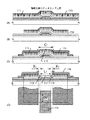
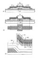
【図1】 薄膜トランジスタの作製工程を示す図。
【図2】 薄膜トランジスタの作製工程を示す図。
【図3】 薄膜トランジスタの構成を示す拡大図。
【図4】 膜中の濃度プロファイルを示す図。
【図5】 薄膜トランジスタの構成を示す図。
【図6】 薄膜トランジスタの構成を示す図。
【図7】 薄膜トランジスタの構成を示す図。
【図8】 CMOS回路の構成を示す図。
【図9】 膜中の濃度プロファイルを示す図。
【図10】 薄膜トランジスタの構成を示す図。
【図11】 CMOS回路の構成を示す図。
【図12】 半導体回路の作製工程を示す図。
【図13】 半導体回路の作製工程を示す図。
【図14】 画素マトリクス回路の構成を示す図。
【図15】 半導体回路の作製工程を示す図。
【図16】 半導体回路の作製工程を示す図。
【図17】 半導体回路の作製工程を示す図。
【図18】 画素マトリクス回路の構成を示す図。
【図19】 画素TFTの構成を示す図。
【図20】 画素TFTの構成を示す図。
【図21】 画素マトリクス回路の構成を示す図。
【図22】 画素TFTの構成を示す図。
【図23】 外部端子取付け部の構成を示す図。
【図24】 半導体回路の露光処理方法に関する構成を示す図。
【図25】 電気光学装置の構成を示す図。
【図26】 電子機器の構成を示す図。
【図27】 半導体回路のパターン構成を示す図。
【図28】 半導体回路のパターン構成を示す図。
【符号の説明】
101 基板
102 下地膜
103 ゲイト電極
104 窒化珪素膜
105 酸化窒化珪素膜
106 非晶質半導体膜
107 ニッケル含有層
108 結晶性半導体膜
109 結晶性半導体膜
110 n+ 層(第1導電層)
111 n- 層(第2導電層)
112 島状半導体層
113 ソース電極
114 ドレイン電極
115 チャネルエッチング領域
116 保護膜
117 チャネル形成領域
118 マスクオフセット領域
119 コンタクトホール[0001]
[Technical field to which the invention belongs]
The present invention relates to a semiconductor device using a semiconductor thin film having a crystal structure and a manufacturing method thereof. In particular, the present invention relates to a structure of an inverted staggered thin film transistor (hereinafter abbreviated as TFT). Further, the present invention relates to a structure of a semiconductor circuit, an electro-optical device, and an electronic device using the TFT.
[0002]
Note that in this specification, “semiconductor device” refers to all devices that can function using semiconductor characteristics, and TFTs, semiconductor circuits, electro-optical devices, and electronic devices described in this specification are all included. It is included in the category of semiconductor devices.
[0003]
[Prior art]
Conventionally, a TFT is used as a switching element of an active matrix liquid crystal display device (hereinafter abbreviated as AMLCD). At present, products having a circuit configuration with TFTs using an amorphous silicon film (amorphous silicon film) as an active layer occupy the market. In particular, as the TFT structure, an inverted stagger structure with a simple manufacturing process is often employed.
[0004]
However, as the performance of AMLCDs increases year by year, the operating performance (especially the operating speed) required for TFTs tends to be severe. Therefore, it has become difficult to obtain an element having sufficient performance at the operating speed of a TFT using an amorphous silicon film.
[0005]
Therefore, TFTs using a polycrystalline silicon film (polysilicon film) instead of an amorphous silicon film have attracted attention, and development of TFTs using a polycrystalline silicon film as an active layer has been proceeding at a remarkable pace. At present, some of them are commercialized.
[0006]
Many presentations have already been made on the structure of an inverted staggered TFT using a polycrystalline silicon film as an active layer. For example, “Fabrication of Low-Temperature Bottom-Gate Poly-Si TFTs on Large-Area Substrate by Linear-Beam Excimer Laser Crystallization and Ion Doping Method: H. Hayashi et.al., IEDM95, PP829-832, 1995” There is a report.
[0007]
This report describes a typical example of an inverted stagger structure using a polycrystalline silicon film (Fig. 4), but there are various problems with such an inverted stagger structure (so-called channel stop type). I have it.
[0008]
First, since the entire active layer is as thin as about 50 nm, impact ionization occurs at the junction between the channel formation region and the drain region, and a deterioration phenomenon such as hot carrier injection appears remarkably. Therefore, it becomes necessary to form a large LDD region (Light Doped Drain region).
[0009]
The controllability of the LDD region becomes the most serious problem. In the LDD region, the control of the impurity concentration and the length of the region is very delicate, and the length control is particularly problematic. At present, a method of defining the length of the LDD region by a mask pattern is adopted. However, as the miniaturization proceeds, a slight patterning error causes a large difference in TFT characteristics.
[0010]
Variation in sheet resistance in the LDD region due to variation in the thickness of the active layer is also a serious problem. Further, variations such as the taper angle of the gate electrode can also cause variations in the effect of the LDD region.
[0011]
Further, in order to form the LDD region, a patterning process is necessary, which directly increases the manufacturing process and decreases the throughput. In the inverted stagger structure described in the above report, it is expected that at least six masks (up to source / drain electrode formation) are necessary.
[0012]
As described above, in the channel stop type inverted stagger structure, it is necessary to form LDD regions in a lateral plane on both sides of the channel formation region, and it is very difficult to form a reproducible LDD region. It is.
[0013]
[Problems to be solved by the present invention]
It is an object of the present invention to provide a technique for manufacturing a semiconductor device with high productivity and high reliability and reproducibility by a very simple manufacturing process.
[0014]
[Means for Solving the Problems]
The configuration of the invention disclosed in this specification is as follows.
A semiconductor device including a source region, a drain region, and a channel formation region that are configured by a semiconductor layer having a crystal structure,
The source region and the drain region are formed of at least a first conductive layer toward the gate insulating film, a second conductive layer having a higher resistance than the first conductive layer, and a semiconductor layer having the same conductivity type as the channel formation region. It has the laminated structure which becomes.
[0015]
In addition, the configuration of other inventions is as follows:
In the above structure, the concentration profile of impurities constituting the first and second conductive layers continuously changes from the first conductive layer to the second conductive layer.
[0016]
In addition, the configuration of other inventions is as follows:
In the above structure, the second conductive layer is 5 × 10 17 ~ 1 × 10 19 atoms / cm Three It is characterized by being formed by impurities that change continuously within the range of.
[0017]
In addition, the configuration of other inventions is as follows:
In the above structure, there are two offset regions having different thicknesses between the channel formation region and the second conductive layer.
[0018]
In addition, the configuration of other inventions is as follows:
In the above structure, an offset region having a thickness larger than that of the channel formation region exists between the channel formation region and the second conductive layer.
[0019]
In addition, the configuration of other inventions is as follows:
A gate electrode formed on a substrate having an insulating surface;
A source region, a drain region, and a channel formation region formed of a semiconductor layer having a crystal structure;
A source electrode and a drain electrode respectively formed on the source region and the drain region;
A semiconductor device comprising:
The source region and the drain region include at least a first conductive layer toward the gate insulating film, a second conductive layer having a higher resistance than the first conductive layer, and a semiconductor layer having the same conductivity type as the channel formation region. Having a laminated structure
The source electrode and / or drain electrode overlaps the gate electrode on the channel formation region.
[0020]
In addition, the configuration of other inventions is as follows:
A semiconductor device including a source region, a drain region, and a channel formation region that are configured by a semiconductor layer having a crystal structure,
The source region and the drain region include at least a first conductive layer toward the gate insulating film, a second conductive layer having a higher resistance than the first conductive layer, and a semiconductor layer having the same conductivity type as the channel formation region. Having a laminated structure
An HRD structure including two offset regions having different thicknesses and the second conductive layer exists between the channel formation region and the first conductive layer.
[0021]
One of the two offset regions having different film thicknesses is an offset in the film surface direction made of a semiconductor layer having the same conductivity type and the same film thickness as the channel formation region, and the other is the same conductivity type as the channel and the It is an offset in the film thickness direction made of a semiconductor layer thicker than the channel formation region.
[0022]
In addition, the configuration of another invention related to the manufacturing method is as follows:
Forming a gate electrode, a gate insulating layer, and an amorphous semiconductor film over a substrate having an insulating surface;
Adding a catalyst element for promoting crystallization to the amorphous semiconductor film, and obtaining a semiconductor film having a crystal structure by heat treatment;
Adding an impurity selected from
A step of gettering the catalytic element with respect to the conductive layer containing the impurities by heat treatment;
Forming a source electrode and a drain electrode on the conductive layer;
Forming a channel formation region by etching the semiconductor film having the crystal structure using the source electrode and the drain electrode as a mask;
Is included in the configuration.
[0023]
In addition, the configuration of other inventions is as follows:
Forming a gate electrode, a gate insulating layer, and an amorphous semiconductor film over a substrate having an insulating surface;
Adding a catalyst element for promoting crystallization to the amorphous semiconductor film, and obtaining a semiconductor film having a crystal structure by heat treatment;
Adding an impurity selected from
A step of gettering the catalytic element with respect to the conductive layer containing the impurities by heat treatment;
Forming a source electrode and a drain electrode on the conductive layer;
Forming a channel formation region by etching the semiconductor film having the crystal structure using the source electrode and the drain electrode as a mask;
Adding a threshold voltage control impurity only to the channel formation region using the source and drain electrodes as a mask;
Is included in the configuration.
[0024]
DETAILED DESCRIPTION OF THE INVENTION
The embodiment of the present invention having the above-described configuration will be described in detail with the examples described below.
[0025]
【Example】
[Example 1]
A typical embodiment of the present invention will be described with reference to FIGS. First, a method for manufacturing a semiconductor device of the present invention will be described with reference to FIGS.
[0026]
A
[0027]
The line width of the
[0028]
As the
[0029]
Next, a silicon nitride film 104 (film thickness is 0 to 200 nm, typically 25 to 100 nm, preferably 50 nm), a silicon oxynitride film or a silicon oxide film (film thickness is 150 to 800) represented by SiOxNy nm, typically 200 to 500 nm, preferably 300 to 400 nm), and an
[0030]
Further, since the present invention has a channel etching type bottom gate structure, the
[0031]
In this embodiment, the
[0032]
In this example, the concentration of each impurity in the formed amorphous silicon film is 5 × 10 5 for carbon and nitrogen. 18 atoms / cm Three Less than (typically 5x10 17 atoms / cm Three Less), oxygen is 1.5 × 10 19 atoms / cm Three Less than (typically 1x10 18 atoms / cm Three The following is controlled. If such management is performed, the impurity concentration finally contained in the channel formation region of the TFT falls within the above range.
[0033]
In this way, the state of FIG. Next, a solution containing a catalytic element (typically nickel) that promotes crystallization of silicon is applied by a spin coating method to form a Ni (nickel) -containing
[0034]
In this publication, although means for applying an aqueous solution containing Ni is shown, the following addition means may be used.
(1) Direct addition by ion implantation or ion doping.
(2) Addition by plasma treatment using a Ni electrode.
(3) Formation of Ni film or Nix Siy (nickel silicide) film by CVD method, sputtering method or vapor deposition method.
[0035]
In addition to Ni, catalytic elements that promote crystallization of silicon include Ge (germanium), Co (cobalt), platinum (Pt), palladium (Pd), iron (Fe), copper (Cu), gold ( Au), lead (Pb), or the like can be used.
[0036]
After the Ni-containing
[0037]
Next, the crystallinity improvement process of the
[0038]
Next, an element selected from Group 15 (typically phosphorus, arsenic or antimony) is added by an ion implantation method (with mass separation) or an ion doping method (without mass separation). In this embodiment, the phosphorus concentration is 1 × 10 × 10 in the range of 30 to 100 nm (typically 30 to 50 nm) from the surface of the
[0039]
In this embodiment, the
[0040]
N + A
[0041]
At this time, the concentration profile in the depth direction when phosphorus is added is very important. This will be described with reference to FIG. The concentration profile shown in FIG. 4 is phosphine (PH) by ion doping with an acceleration voltage of 80 keV and an RF power of 20 W. Three ) Is added.
[0042]
In FIG. 4, 401 indicates a crystalline silicon film, and 402 indicates a concentration profile of added phosphorus. This concentration profile is determined by setting conditions such as RF power, added ion species, and acceleration voltage.
[0043]
At this time, the peak value of the concentration profile 402 is n + The phosphor concentration decreases with increasing depth in the crystalline silicon film 401 (or toward the gate insulating film) inside the
[0044]
And this n - Even within the
[0045]
Further, the region where the phosphorus concentration is extremely lowered and the lower layer thereof become an intrinsic or substantially intrinsic region (i layer) 405. Note that an intrinsic region is a region to which no impurity is intentionally added. In addition, a substantially intrinsic region is a region where the impurity concentration (here phosphorus concentration) is lower than the spin density of the silicon film or the impurity concentration is 1 × 10 14 ~ 1 × 10 17 atoms / cm Three A region showing one conductivity in the range of.
[0046]
Such intrinsic or substantially intrinsic regions are n - Formed below
[0047]
In this way, n + By using ion implantation or ion doping to form the layer, n + N under the layer - A layer can be formed. N as before + Such a configuration cannot be realized when the layers are provided by film formation. In addition, by appropriately setting the conditions at the time of ion addition, n + Layer and n - The layer thickness can be easily controlled.
[0048]
In particular, n - Since the thickness of the
[0049]
Next, when the state shown in FIG. 1E is obtained, heat treatment is performed at a temperature of 500 to 700 ° C. (typically 600 to 650 ° C.) for 0.5 to 8 hours (typically 1 to 4 hours). Furnace annealing), the Ni in the i layer is changed to n + / N - Move to layer. At this time, Ni is gettered substantially in the direction of the arrow. (Fig. 2 (A))
[0050]
Thus, the present embodiment is n + Layers 110, n - Phosphorus contained in
[0051]
In this case, since the distance that Ni should move is only a distance corresponding to the thickness of the crystalline silicon film, gettering is completed very quickly (within a short time). Therefore, (1) a decrease in the concentration of phosphorus to be added, (2) a decrease in the heat treatment temperature, and (3) a reduction in the heat treatment time can be realized.
[0052]
In this embodiment, since the TFT is manufactured on the glass substrate, the maximum process temperature is determined by the heat resistance of the glass. However, if a highly heat-resistant substrate such as a quartz substrate is used as the substrate, the maximum temperature for heat treatment for gettering can be increased to 1000 ° C. (preferably 800 ° C.). If the temperature exceeds 800 ° C., the reverse diffusion of phosphorus from the gettering region to the gettering region begins to occur, which is not preferable.
[0053]
The reason why the heat resistance of the
[0054]
In this way, the catalytic element is n + / N - When gettering to the layer, the Ni concentration in the i layer is 5 × 10 17 atoms / cm Three Reduced to: Currently, 2 × 10 due to the detection limit of SIMS (mass secondary ion analysis) 17 atoms / cm Three It can only be seen that it is less than or equal to the spin density in the i layer (1 × 10 14 atoms / cm Three Is expected to be reduced.
[0055]
After the catalytic element gettering step is completed, the crystalline silicon film is patterned to form the island-shaped
[0056]
Here, although not shown in the drawing, a part of the exposed gate insulating layer is etched to make electrical connection between the gate electrode (first wiring) and the electrode (second wiring) to be formed next. A hole (a region indicated by 119 in FIG. 2D) is opened. Here, a third patterning step is performed.
[0057]
Next, a conductive metal film (not shown) is formed, and the
[0058]
As will be described later, the length (C) of a region (hereinafter referred to as a channel etching region) 115 directly above the
[0059]
Next, dry etching is performed using the
[0060]
At this time, n + Layer 110 is completely etched and stops etching leaving only intrinsic or substantially intrinsic regions (i-layer). In the present invention, finally, only the semiconductor layer of 10 to 100 nm (typically 10 to 75 nm, preferably 15 to 45 nm) is left. In this embodiment, a semiconductor layer having a thickness of 30 nm is left.
[0061]
When the etching of the island-like semiconductor layer 112 (channel etching process) is completed in this way, a silicon oxide film or a silicon nitride film is formed as the
[0062]
In this state, in the island-shaped
[0063]
In this embodiment, the line width (L 1 Is 3 μm and the length of the channel etching region 115 (C 1 ) Is 4 μm, the length of the offset region (X 1 ) Is 0.5μm.
[0064]
Here, an enlarged view of the drain region (semiconductor layer in contact with the drain electrode 114) is shown in FIG. In FIG. 3, 103 is a gate electrode, 301 is a channel formation region, 302 is n + Layer (source or drain electrode), 303 and 304 are offset regions having different film thicknesses, and 305 is n - Layer (LDD region).
[0065]
Note that although not described here, the source region (semiconductor layer in contact with the source electrode 113) also has a similar structure.
[0066]
Further, although the structure shown in FIG. 3 is schematically shown, attention should be paid to the film thickness relationship in each region. The most preferable configuration for configuring the present invention is that the thickness of the film is n. + Layer 302 <n - This is a case where the relationship of layer 305 <offset region (i layer) 304 is satisfied.
[0067]
Because n + Since the layer 302 only functions as an electrode, it is sufficient to be thin. On the other hand, n - The layer 305 and the offset
[0068]
In the configuration of this embodiment, the
[0069]
[0070]
The present inventors call such a structure composed of offset + LDD as an HRD (High Resistance Drain) structure, and distinguish it from a normal LDD structure. In the case of the present embodiment, the HRD structure is constituted by a three-stage structure of mask offset + thickness offset + LDD.
[0071]
At this time, since the
[0072]
Note that the length of the mask offset region 303 (X 1 ) Is controlled by patterning, and therefore is affected by errors due to patterning and shrinkage of glass. However, since the thickness offset
[0073]
Note that the length of the mask offset (X 1 ) Is the channel length (L 1 ) And the length of the channel etching region (C 1 ) (C 1 -L 1 ) / 2. Therefore, a desired offset length (X 1 ) Can be set. In the configuration of this embodiment, the offset length (X 1 ) Can be 0.3 to 3 μm (typically 1 to 2 μm).
[0074]
Note that an inverted staggered TFT having a structure as shown in FIG. 2D cannot be realized by a conventional TFT using an amorphous silicon film as an active layer (island semiconductor layer). This is because, when an amorphous silicon film is used, the mobility of carriers (electrons or holes) becomes extremely slow unless the source / drain electrode and the gate electrode overlap each other.
[0075]
Even if the source / drain electrode and the gate electrode overlap each other, the mobility (field effect mobility) of the TFT using the amorphous silicon film is at most 1 to 10 cm. 2 It is about / Vs. On the other hand, if the structure as in this embodiment is adopted, the mobility is too low to function as a switching element.
[0076]
However, since the crystalline silicon film is used as the active layer in the present invention, the carrier mobility is sufficiently fast. Therefore, sufficient mobility can be obtained even with the structure as in this embodiment. That is, the structure of this embodiment can be realized only by using a semiconductor film having a crystal structure as a semiconductor layer.
[0077]
In addition, since the inverted staggered TFT of this embodiment has an HRD structure, it is very strong against deterioration phenomena such as hot carrier injection due to impact ionization and has high reliability. Moreover, the effect of the LDD region is dominant, and the LDD region is formed with very good controllability, so that the variation in characteristics is very small.
[0078]
For this reason, the structure as in this embodiment is suitable for a TFT that constitutes a circuit that requires a high breakdown voltage and does not require a high operation speed.
[0079]
Further, as shown in the manufacturing process of this embodiment, only four masks are required to obtain an inverted staggered TFT having the structure shown in FIG. This means that the throughput and the yield are dramatically improved considering that the conventional channel stop type TFT requires six masks.
[0080]
As described above, according to the structure of this embodiment, a bottom gate type TFT having high reliability and reproducibility can be manufactured by a manufacturing process with high mass productivity.
[0081]
Note that the mobility of a bottom gate type TFT (N-channel type TFT) manufactured according to the manufacturing process of this example is 30 to 250 cm. 2 / Vs (typically 10-150cm 2 / Vs), the threshold voltage can be 0-3V.
[0082]
[Example 2]
In the present embodiment, a configuration example different from the first embodiment in the configuration of the present invention is shown. Since the TFT manufacturing process may basically follow the first embodiment, only necessary portions will be described in this embodiment.
[0083]
First, the state shown in FIG. 5A is obtained in accordance with the manufacturing process of Example 1. Here, the difference from the first embodiment is that the length of the
[0084]
In this state, when the channel etching process is performed as shown in the first embodiment and a protective film is provided, the state shown in FIG. 5B is obtained. At this time, a region indicated by 503 is a channel formation region, and the channel length is L 2 (= C 2 ). In addition, the length (Y 2 ) Where E is the gate electrode width, 2 ) / 2.
[0085]
FIG. 5C is an enlarged view of the drain region. In the TFT operation, carriers are channel formation region 503 (
[0086]
In this case, an electric field from the gate electrode is also formed in the
[0087]
As described above, in the structure of this embodiment, the HRD structure is constituted by substantial LDD due to overlap + LDD due to thickness offset + low concentration impurities. Further, when the thickness of the
[0088]
Even in the configuration of the present embodiment, the
[0089]
Note that the structure as in this embodiment is suitable for a TFT constituting a circuit that has a small offset component and requires a high operating speed.
[0090]
In addition, the structure of this embodiment has an advantage that the substrate floating effect is unlikely to occur because minority carriers accumulated in the channel formation region due to impact ionization are quickly extracted to the source electrode. Therefore, it is possible to realize a TFT having a high operation speed and a very high breakdown voltage characteristic.
[0091]
Example 3
In the present embodiment, a configuration example different from the first and second embodiments in the configuration of the present invention is shown. Since the TFT manufacturing process may basically follow the first embodiment, only necessary portions will be described in this embodiment.
[0092]
First, the state shown in FIG. 6A is obtained in accordance with the manufacturing process of Example 1. Here, the difference from the first embodiment is that the length of the
[0093]
In this state, when the channel etching process is performed as shown in the first embodiment and a protective film is provided, the state shown in FIG. 6B is obtained. At this time, a region indicated by 603 becomes a channel formation region, and the channel length is L Three (= C Three ).
[0094]
FIG. 6C is an enlarged view of the drain region. In the TFT operation, carriers are channel formation region 603 (thickness 100 nm), thickness offset region 604 (thickness 150 nm), and LDD region 605 (thickness). 100 nm) through n + The layer 606 (
[0095]
Also in the configuration of this embodiment, the thickness offset
[0096]
Example 4
In the present embodiment, a configuration example different from the first to third embodiments in the configuration of the present invention is shown. Since the TFT manufacturing process may basically follow the first embodiment, only necessary portions will be described in this embodiment.
[0097]
First, the state of FIG. 7A is obtained in accordance with the manufacturing process of Example 1. Here, the difference from the first embodiment is that when the
[0098]
In this embodiment, the length of the
[0099]
In this state, when a channel etching process is performed as shown in the first embodiment and a protective film is provided, the state shown in FIG. 7B is obtained. At this time, a region indicated by 703 becomes a channel formation region, and the channel length is L Four (= C Four -X Four ).
[0100]
Where X Four Is the length of the mask offset region 704. X Four For the numerical range, reference may be made to Example 1. Further, the numerical range of the length of the
[0101]
In this example, the HRD structure described in Example 1 and the HRD structure (or LDD structure) described in Example 2 are combined. Since the structural description has already been described in the first and second embodiments, the description thereof is omitted here.
[0102]
When the structure as in this embodiment is employed, it is particularly preferable to use the HRD structure (or LDD structure) shown in Embodiment 2 for the source region and the HRD structure described in
[0103]
For example, an electric field concentration is particularly intense at the channel end (junction) on the drain region side, and an HRD structure having a large resistance component as shown in the first embodiment is desirable. On the other hand, since there is no need for such a high withstand voltage countermeasure on the source side, an HRD (or LDD) structure with a small resistance component as shown in the second embodiment is suitable.
[0104]
In this embodiment, the configuration of Embodiment 2 can be combined with either one of the source / drain regions. As described above, the HRD structure or the LDD structure shown in the first to third embodiments may be appropriately selected by the practitioner and used in the source / drain region, and an optimum structure may be designed in view of circuit design. In this case, 3 2 = 9 possible combination patterns.
[0105]
Example 5
In this embodiment, an example in which a CMOS circuit (inverter circuit) is formed using bottom gate TFTs having the configurations shown in
[0106]
FIG. 8 shows a CMOS circuit using the configuration shown in the fourth embodiment, in which 801 is a PTFT source electrode, 802 is an NTFT source electrode, and 803 is an N / P common drain electrode.
[0107]
In addition, NTFT is formed by the manufacturing process described in the first embodiment. +
[0108]
Note that it is very easy to manufacture a CMOS circuit on the same substrate. In the case of the present invention, first, the state of FIG.
[0109]
In this state, an element selected from the
[0110]
In this embodiment, boron is taken as an example. At this time, boron is at least three times the concentration of phosphorus (typically 3 × 10 19 ~ 1 × 10 twenty two atoms / cm Three , Preferably 3 × 10 20 ~ 3 × 10 twenty one atoms / cm Three ) To reverse the conductivity. N + Layers and n - Completely p all layers ++ Layer and p - In order to reverse the layer, it is important to adjust the concentration profile at the time of boron addition and add it deeper than the addition depth of phosphorus.
[0111]
Therefore, the concentration profile of boron in the film is as shown in FIG. In FIG. 9, 900 is a semiconductor layer, 901 is a phosphorus concentration profile before boron addition, 902 is a boron concentration profile after boron addition, and 903 is p ++ Layer, 904 is p - Layer 905 is the i layer.
[0112]
At this time, p ++ The thickness of the
[0113]
By the way, in this example, both NTFT and PTFT use the HRD structure (type using an overlap region) of the configuration shown in Example 2 on the source region side, and the example shown on Example 1 on the drain region side. An HRD structure (type using a mask offset) is provided.
[0114]
Therefore, as apparent from the top view, the PTFT has an overlap region having a length Yi on the source region side and a mask offset region having a length Xi on the drain region side. The NTFT has an overlap region having a length of Yj on the source region side and a mask offset region having a length of Xj on the drain region side.
[0115]
At this time, the lengths of Xi and Xj and Yi and Yj can be freely adjusted by mask design. Therefore, each length may be determined as appropriate according to the circuit configuration, and it is not necessary to arrange the lengths of the N-channel type and the P-channel type.
[0116]
In addition, with such a structure, the breakdown voltage characteristics of the region serving as the common drain of the CMOS circuit can be increased, which is a very effective configuration when configuring a circuit with a high operating voltage.
[0117]
Although the configuration of the CMOS circuit using the TFT having the configuration shown in Examples 1 to 4 is shown in FIG. 8, it goes without saying that all other combinations are possible. Since there are nine possible configuration patterns for one TFT, it is 9 in the CMOS circuit. 2 There are 81 ways. Among these combinations, an optimal combination may be adopted according to the performance required by the circuit.
[0118]
Further, as shown in this embodiment, the present invention can be easily applied to PTFTs. In that case, the mobility of the bottom gate type TFT (PTFT) of the present invention is 30 to 150 cm. 2 / Vs (typically 10-100cm 2 / Vs), the threshold voltage can be -1 to -3V.
[0119]
Example 6
In this embodiment, an example in which Ge (germanium) is used as a catalyst element for promoting crystallization of silicon will be described. In the case of using Ge, addition by ion implantation, ion doping, or plasma treatment is preferably performed because of its high versatility. Moreover, it is also possible to add from the vapor phase by performing a heat treatment in an atmosphere containing Ge.
[0120]
Since Ge is an element belonging to the
[0121]
Therefore, when the amorphous silicon film using Ge is crystallized as in this embodiment, there is no need to getter the catalytic element after crystallization. Of course, a gettering step may be performed, but the TFT characteristics are not affected.
[0122]
Accordingly, the heat treatment in the gettering process can be omitted, and the throughput of the manufacturing process is greatly improved. Si x Ge 1-x Since a TFT using a film is known to exhibit high mobility, an improvement in operation speed can be expected if the Ge content in the silicon film is appropriate.
[0123]
Note that the configuration of this embodiment can be applied to any of the configurations of the first to fifth embodiments.
[0124]
Example 7
In this embodiment, an example will be described in which a device for controlling the threshold voltage is applied to the TFT of the present invention.
[0125]
In order to control the threshold voltage, an element selected from group 13 (typically boron, indium, gallium) or group 15 (typically phosphorus, arsenic, antimony) is added to the channel formation region. The technique is called channel doping.
[0126]
Channel doping is effective for the present invention, and the following two methods may be simple.
[0127]
First, at the time of forming an amorphous silicon film, a gas containing impurities for controlling a threshold voltage (for example, diborane, phosphine, etc.) is mixed in a film forming gas, and a predetermined amount is included simultaneously with film formation. There is. In this case, it is not necessary to increase the number of processes at all, but since the same concentration is added to both the N-type and P-type TFTs, it is not possible to meet the demand for different concentrations between the two.
[0128]
Next, after the channel etching step (channel forming region forming step) as described in FIG. 2D is completed, the channel forming region (or the channel forming region and the mask offset region) is formed using the source / drain electrodes as a mask. There is a method of selectively adding impurities.
[0129]
As an addition method, various methods such as an ion implantation method, an ion doping method, a plasma treatment method, a gas phase method (diffusion from an atmosphere), and a solid phase method (diffusion from the film) can be used. Since it is thin, a method that does not give damage, such as a gas phase method or a solid phase method, is preferable.
[0130]
Note that when an ion implantation method or the like is used, damage to the channel formation region can be reduced if a protective film that covers the entire TFT is provided.
[0131]
Further, after the impurity is added, an impurity activation step is performed by laser annealing, lamp annealing, furnace annealing, or a combination thereof. At this time, the damage received by the channel formation region is almost recovered.
[0132]
When implementing this example, the channel formation region is 1 × 10 15 ~ 5 × 10 18 atoms / cm Three (Typically 1 × 10 15 ~ 5 × 10 17 atoms / cm Three ) To add an impurity for controlling the threshold voltage.
[0133]
When this embodiment is applied to the TFT of the present invention, the threshold voltage of the N-channel TFT can be kept in the range of 0.5 to 2.5V. When applied to a P-channel TFT, the threshold voltage can be kept within the range of -0.1 to -2.0V.
[0134]
In addition, the structure of a present Example can be combined with any structure of Examples 1-6. Further, when applied to the CMOS circuit of Example 5, the N-type TFT and the P-type TFT can have different addition concentrations and different types of impurities to be added.
[0135]
Example 8
In the structure shown in FIG. 2D, the
[0136]
The structure shown in FIG. 10A is basically similar to FIG. 2D, but is characterized in that the shapes of the
[0137]
A region indicated by 13 is a region having the same film thickness as the
[0138]
Here, the characteristics of this embodiment will be described in the light of the manufacturing process. In this embodiment, the
[0139]
When the channel etching process is performed in this state, the island-
[0140]
In this way, a structure as shown in FIG. Therefore, it is clear that the
[0141]
There are the following two reasons for forming the protruding
(1) Used as an etching monitor in a channel etching process.
(2) When a protective film or an interlayer insulating film is formed in a later process, coverage defects due to steps in the island-shaped semiconductor layer are reduced.
[0142]
The etching monitor is used when inspecting whether or not the channel formation region has an appropriate film thickness by sampling inspection in the manufacturing process.
[0143]
In addition, the structure of a present Example can be combined with any structure of Examples 1-7.
[0144]
Example 9
In this embodiment, an example of the circuit configuration of the CMOS circuit (inverter circuit) shown in
[0145]
FIG. 11A shows a CMOS circuit having the same structure as that shown in FIG. In this case, the circuit configuration includes a
[0146]
Note that the terminal portions a, b, c, and d correspond to the terminal portions a, b, c, and d of the inverter circuit shown in FIG.
[0147]
Next, FIG. 11B shows an example in which a semiconductor layer serving as a drain region is shared between an N-type TFT and a P-type TFT. Each code corresponds to the code described in FIG.
[0148]
In the structure shown in FIG. 11B, TFTs can be formed at a very high density, which is very effective when a circuit is highly integrated. The common semiconductor layer forms a PN junction, but this is not a problem.
[0149]
Example 10
In this embodiment, an example in which lamp annealing is used as a heat treatment means in the process of manufacturing TFTs and CMOS circuits having the configurations of
[0150]
As lamp annealing, heat treatment by RTA (Rapid Thermal Anneal) is known. This is a technique for performing high-temperature heat treatment in a short time (several seconds to several tens of seconds) by irradiating strong light from an infrared lamp, and has a very high throughput. In addition to infrared light, ultraviolet light may be used supplementarily.
[0151]
In the present invention, heat treatment is performed in the crystallization process of the amorphous semiconductor film, the crystallinity improvement process of the crystalline semiconductor film, the gettering process of the catalytic element, the impurity activation process for threshold control, and the like. . In this case, the present embodiment can be used.
[0152]
Note that the configuration of this embodiment and the configurations of other embodiments can be freely combined.
[0153]
Example 11
In this embodiment, a case where gettering of a catalytic element is performed by means different from that in
[0154]
In Example 1, the gettering process is performed using only elements selected from
[0155]
In that case, after obtaining the state shown in FIG. 1E, only the region to be an N-channel TFT is hidden with a resist mask, and then boron is added. That is, only phosphorus exists in a region to be an N-channel TFT, and only boron exists in a region to be a P-channel TFT.
[0156]
Then, heat treatment may be performed in that state to perform a catalyst element gettering step. In our experiment, it has been confirmed that the gettering effect by phosphorus + boron is higher than the gettering effect by phosphorus alone. However, there was no gettering effect with boron alone, and a high gettering effect was obtained when the combination of boron and phosphorus at a higher concentration than phosphorus was used.
[0157]
Note that the configuration of this embodiment and the configurations of other embodiments can be freely combined.
[0158]
Example 12
If a quartz substrate or silicon substrate with high heat resistance is used as the substrate, n + Conductive layer and n - It is also effective to perform a heat treatment at about 700 to 1100 ° C. in an oxidizing atmosphere containing a halogen element before forming the conductive layer. This is a technique that utilizes the gettering effect of a metal element by a halogen element.
[0159]
Further, by using this technique in combination with the gettering process as shown in
[0160]
Example 13
In this embodiment, an example of manufacturing an active matrix display device in which a driver circuit (peripheral driver circuit) and a pixel matrix circuit are integrally formed over the same substrate in accordance with the basic manufacturing process described in
[0161]
In this embodiment, a CMOS circuit (type shown in FIG. 11B) which is a basic configuration is shown as a driver circuit. In addition to the driver circuit, a signal processing circuit such as a D / A converter circuit, a memory circuit, and a γ correction circuit (referred to as a logic circuit in order to distinguish them from the driver circuit) can be configured with the TFT of the present invention. It is. In this case, a CMOS circuit is used as a basic circuit.
[0162]
An example in which a multigate TFT is used as the pixel matrix circuit is shown. In this embodiment, an example of a double gate structure is shown, but a single gate structure or a triple gate structure may be used.
[0163]
First, the process up to the step shown in FIG. 2A (catalyst element gettering step) is completed using the manufacturing step of the first embodiment. This state is shown in FIG.
[0164]
In FIG. 12A, 30 is a glass substrate, 31 is a base film, 32 is a gate electrode of PTFT which becomes a CMOS circuit, and 33 is a gate electrode of NTFT.
[0165]
Further, a
[0166]
Next, a gettering step by RTA treatment is performed to getter the catalytic element (nickel according to the first embodiment) contained in the
[0167]
Next, boron which is an element selected from the
[0168]
Next, a laser annealing process is performed to improve the crystallinity of the crystalline semiconductor layer that has been amorphized in the ion implantation process (or ion doping process). In addition, the impurities (phosphorus and boron) added at the same time are activated. (Figure 12 (C))
[0169]
If dehydrogenation by RTA treatment is performed before this laser annealing step, a hydrogen bumping phenomenon can be prevented during laser annealing.
[0170]
Next, the crystalline semiconductor layer is etched to form island-shaped semiconductor layers 43 and 44. At this time, a contact hole is formed in order to connect a part of the electrode (second wiring) to be formed next and the gate wiring.
[0171]
Note that the laser annealing step described above can be performed after the crystalline semiconductor layer is processed into an island-shaped semiconductor layer.
[0172]
Then, a conductive thin film is formed and patterned to form source electrodes 45 (NTFT) and 46 (PTFT) and a
[0173]
When the state of FIG. 13A is obtained, a channel etching step is performed to form
[0174]
Further, as shown in FIG. 13B, the pixel TFT has a configuration in which a mask offset region is provided on the side connected to the
[0175]
Since the source / drain regions of the pixel TFT are switched during charging / discharging of the video signal, it is necessary to increase the breakdown voltage at both ends of the TFT. Also, if the resistance component below the
[0176]
In addition, this Example is an example considered to be the most preferable, and this Example is not limited to this structure. The practitioner may select an optimum structure by taking advantage of each structure described in the first to fourth embodiments.
[0177]
Next, a
[0178]
Next, a contact hole is formed in the
[0179]
Thereafter, an active matrix type liquid crystal display device can be manufactured by sandwiching a liquid crystal layer between a counter substrate and an active matrix substrate using a known cell assembling process.
[0180]
Note that the number of times of patterning necessary for manufacturing the active matrix substrate shown in this embodiment is seven. The process is shown below.
(1) Gate electrode patterning
(2) Boron added region patterning
(3) Island-like semiconductor layer patterning
(4) Gate contact patterning
(5) Source / drain electrode patterning
(6) ITO contact patterning
(7) ITO patterning
[0181]
As described above, since the active matrix substrate can be manufactured with a very small number of masks, the throughput is significantly improved. At the same time, since the circuit can be freely designed using the TFTs having the configurations shown in
[0182]
Note that FIG. 14A illustrates a part of the pixel matrix circuit described in this embodiment as viewed from above. In FIG. 14A, the reference numerals used in the present embodiment are basically attached. Therefore, only necessary parts will be described.
[0183]
FIG. 14B is a cross-sectional view taken along the line AA ′ in FIG. 14A. Although not shown in FIG. 13C, a
[0184]
The
[0185]
Example 14
In this example, an example in which an active matrix display device is manufactured with a structure different from the process shown in Example 13 is shown.
[0186]
The feature of the present embodiment is that after the crystallization using the catalytic element, the crystallinity improving step by laser annealing is not performed. That is, after crystallization, the phosphorus addition step, the catalytic element gettering step, and the like are performed in the same manner as in Example 13.
[0187]
The feature of this embodiment is that the crystallinity improvement step (impurity activation, recrystallization, etc.) in the channel formation region is performed after the
[0188]
When laser annealing is performed in the state shown in FIG. 15, the back diffusion (Out Diffusion) of impurities such as phosphorus and boron from the source / drain regions can be suppressed. Further, it is possible to obtain an advantage that the power (laser energy) of the laser light is about half.
[0189]
In addition, a present Example is not limited to the structure shown by drawing. The practitioner may perform circuit design by selecting an optimum structure by taking advantage of each TFT structure described in the first to fourth embodiments. In addition, this embodiment can be combined with the configuration shown in all other embodiments.
[0190]
Example 15
In this example, an example in which the laser annealing step after crystallization is omitted in Example 13 is shown. In this embodiment, after the crystallization step, phosphorus is added using an ion doping method and a gettering step of the catalytic element is performed by RTA.
[0191]
Then, boron is added by ion doping, and p is formed on the semiconductor layer to be a PTFT. ++
[0192]
In this state, an annealing process using RTA is performed. In this embodiment, activation of impurities (phosphorus and boron) added by annealing with RTA and dehydrogenation of the semiconductor layer (since ion doping without mass separation causes hydrogen to be implanted together with phosphorus and boron). It is carried out. (FIG. 16 (A))
[0193]
Next, a laser annealing process is performed to recrystallize the semiconductor layer that has been amorphized in the impurity addition process, thereby improving crystallinity. This laser annealing step may be performed after the semiconductor layer is etched and processed into an island-shaped semiconductor layer.
[0194]
Subsequent steps may follow Example 13. In addition, a present Example is not limited to the structure shown by drawing. The practitioner may perform circuit design by selecting an optimum structure by taking advantage of each TFT structure described in the first to fourth embodiments. In addition, this embodiment can be combined with the configuration shown in all other embodiments.
[0195]
Example 16
This embodiment shows an example in which an active matrix substrate is manufactured using a configuration different from those of Embodiments 13-15.
[0196]
First, phosphorus is added to the crystalline semiconductor layer formed in accordance with the steps of Example 1. N + Layer 38, n - Layer 39 and
[0197]
Next, annealing by RTA is performed to perform a gettering step of the catalyst element (in this embodiment, nickel). The feature of this embodiment is that the NTFT can obtain the gettering effect by phosphorus, and the PTFT can obtain the gettering effect by phosphorus + boron. (Fig. 17 (C))
[0198]
When the state of FIG. 17C is obtained in this way, a laser annealing step is performed to improve the crystallinity of the semiconductor layer that has become amorphous by the addition of impurities. Note that the gettering step by RTA shown in FIG. 17B also serves as dehydrogenation of the semiconductor layer. Therefore, even if a large amount of hydrogen is present in the film due to the addition of impurities, the bumping phenomenon of hydrogen does not occur.
[0199]
Note that the recrystallization step by laser annealing may be performed after the semiconductor layer is etched and processed into an island-shaped semiconductor layer.
[0200]
Subsequent steps may follow Example 13. In addition, a present Example is not limited to the structure shown by drawing. The practitioner may perform circuit design by selecting an optimum structure by taking advantage of each TFT structure described in the first to fourth embodiments. In addition, this embodiment can be combined with the configuration shown in all other embodiments.
[0201]
Example 17
In this embodiment, an example of manufacturing a reflective liquid crystal display device based on the manufacturing process shown in
[0202]
In addition, the same part as the part demonstrated in Example 13 is attached | subjected and shown with the same code | symbol, and detailed description is abbreviate | omitted. Further, FIG. 18B shows a cross-sectional view of FIG. 14A cut along BB ′.
[0203]
First, the difference from the thirteenth embodiment is that the
[0204]
In the case of this embodiment, the
[0205]
The pixel electrode 61 is a reflective electrode, and it is preferable to use aluminum having a high reflectance or a material mainly composed of aluminum. If the liquid crystal display device of this embodiment is used for a projection display device, the surface of the pixel electrode is preferably flat. On the other hand, if it is used for a direct-view display device, it is necessary to devise a method for widening the viewing angle by increasing the irregular reflectance by providing irregularities on the surface.
[0206]
In addition, a present Example is not limited to the structure shown by drawing. The practitioner may perform circuit design by selecting an optimum structure by taking advantage of each TFT structure described in the first to fourth embodiments. In addition, this embodiment can be combined with the configuration shown in all other embodiments.
[0207]
Example 18
In this embodiment, a description will be given of the configuration of a BM (black matrix) in the liquid crystal display device shown in the thirteenth embodiment.
[0208]
First, the formation of the
[0209]
After obtaining the state of FIG. 19A, a black resin (not shown) is formed on the entire surface. As the black resin, an organic resin film containing graphite, carbon, pigment, or the like can be used. For the organic resin film, polyimide, acrylic, or the like is used. In this embodiment, a photosensitive acrylic resin in which graphite is dispersed is used.
[0210]
When the black resin is formed in this way, it is possible to selectively expose only the region where the
[0211]
After the
[0212]
As described above, an active matrix substrate having a structure as shown in FIG. 19B is completed. After that, if a known cell assembling process is performed, a liquid crystal display device can be manufactured. The black matrix as in this embodiment has an advantage that no parasitic capacitance is formed with other wirings.
[0213]
In addition, a present Example is not limited to the structure shown by drawing. The practitioner may perform circuit design by selecting an optimum structure by taking advantage of each TFT structure described in the first to fourth embodiments. In addition, this embodiment can be combined with the configuration shown in all other embodiments.
[0214]
Example 19
In this embodiment, an example in which a black matrix different from that in Embodiment 18 is used will be described. Specifically, an example in which a conductive film is used as the black matrix is shown.
[0215]
In FIG. 20,
[0216]
In addition, since the black matrix of this embodiment is conductive, there are various utilization methods other than the role as the black matrix. First, a pattern indicated by 71 is a black matrix fixed at a common potential (ground potential). A pattern indicated by 72 is connected to the drain electrode of the CMOS circuit and used as a lead-out wiring. In this way, a multilayer wiring structure can be easily realized by using this embodiment.
[0217]
A
[0218]
Then, an
[0219]
After the
[0220]
Here, an arrangement example of the black matrix of the pixel matrix circuit is shown in FIG. FIG. 21 shows an arrangement example when the
[0221]
The
[0222]
In addition, a present Example is not limited to the structure shown by drawing. The practitioner may perform circuit design by selecting an optimum structure by taking advantage of each TFT structure described in the first to fourth embodiments. In addition, this embodiment can be combined with the configuration shown in all other embodiments.
[0223]
Example 20
In this example, an example in which an active matrix substrate is manufactured with a TFT structure different from the structure shown in Example 13 will be described.
[0224]
The most important point in the structure shown in FIG. 22 is that the uppermost portion of each semiconductor layer (source / drain region) is the first conductive layer (n + Region or p ++ Each conductive layer is once covered with the
[0225]
In the case of such a structure, a channel etching process for forming a channel formation region is performed using a resist mask. Then, a
[0226]
As in the structure of the present embodiment, each of the extraction electrodes (functioning as source / drain electrodes or routing wiring) 87 to 91 is separated from the gate electrode by the
[0227]
Note that the structure of this embodiment can also be applied to the TFTs shown in
[0228]
Example 21
In this example, a connection structure with an external terminal in the active matrix substrate having the structure shown in Examples 13 to 21 will be described. 23 is an enlarged view of a terminal portion (hereinafter referred to as an FPC attachment portion) connected to an external terminal (typically a flexible printed circuit (FPC)), and is located at an end portion of the active matrix substrate. To do.
[0229]
In FIG. 23,
[0230]
The feature of this embodiment is that the
[0231]
Further, in the FPC attachment portion, the
[0232]
When the anisotropic
[0233]
Then, when the FPC attachment portion has a structure as shown in FIG. 23, the
[0234]
[Example 22]
In this embodiment, a device for improving the patterning efficiency in forming the TFT of the present invention on a large glass substrate will be described.
[0235]
When a fine semiconductor circuit is manufactured over a large glass substrate, patterning errors due to warpage or shrinkage of the glass substrate become a problem. Therefore, an exposure method using an exposure apparatus called a stepper has attracted attention. In stepper exposure, only a part of one reticle can be partially exposed.
[0236]
In the case of this embodiment, necessary circuit patterns such as a driver circuit and a pixel matrix circuit are formed for each part on one reticle. Further, at this time, a region where the same structure is repeated is formed by repeated exposure of the same circuit pattern.
[0237]
In FIG. 24, A, C, G, and I patterns are circuit patterns for producing end portions of the driver circuit. B and H patterns are horizontal circuit patterns of the horizontal scanning driver circuit, and D and F patterns are vertical circuit patterns of the vertical scanning driver circuit. The E pattern is a repeated circuit pattern of the pixel matrix circuit.
[0238]
In this way, driver circuits and pixel matrix circuits that are configured by continuously connecting circuits with the same structure are formed with dedicated circuit patterns only at the ends, and the same circuit pattern is completely repeated inside. The entire pattern is formed using this.
[0239]
When this method is used, the circuit pattern can be shared, so that the number of circuit patterns written on one reticle is reduced, and the reticle can be reduced. In addition, since a single reticle can be used for any large substrate, the time for mask change is saved and the throughput is improved.
[0240]
For example, when the pixel matrix circuit is SXGA, 1280 pixels are arranged in the row direction and 1024 pixels are arranged in the column direction. Therefore, if a pattern circuit corresponding to 256 pixels is written in the row direction of the above-mentioned E pattern, the row direction is completed by repeated exposure five times. In addition, if a pattern circuit corresponding to 256 pixels is written in the column direction, the column direction ends with four repeated exposures.
[0241]
As described above, when the number of repeated exposures in the row direction and the column direction is n and m, respectively, and the numbers of pixels in the row direction and the column direction are X and Y, respectively, the circuit pattern for forming the pixel matrix circuit includes a row It is necessary to write a pixel pattern of X / n in the direction and Y / m in the column direction. By utilizing this regularity, a high-definition display such as 1920 × 1080 pixels such as ATV (Advanced TV) can be easily realized.
[0242]
Example 23
In this embodiment, an example in which an AMLCD (active matrix liquid crystal display device) is formed using the active matrix substrate having the structure shown in
[0243]
Here, the appearance of the AMLCD of this embodiment is shown in FIG. In FIG. 25A,
[0244]
In the AMLCD of this embodiment, an
[0245]
Further,
[0246]
Further, a configuration as shown in FIG. In FIG. 25B, the same portions as those in FIG. 25A are denoted by the same reference numerals. Here, an example is shown in which the signal processing performed by the IC chip in FIG. 25A is performed by a
[0247]
In this case, the
[0248]
In addition to the switching element of AMLCD, the TFT using the present invention can be used as a switching element of an EL (electroluminescence) display device. Further, a circuit such as an image sensor can be constituted by the bottom gate type TFT of the present invention.
[0249]
As described above, various electro-optical devices can be manufactured with TFTs using the present invention. In this specification, an electro-optical device is defined as a device that converts an electrical signal into an optical signal and vice versa.
[0250]
In manufacturing the AMLCD of this embodiment, the black matrix may be provided on the counter substrate side, or may be provided on the active matrix substrate (BM on TFT).
[0251]
Further, color display may be performed using a color filter, or the liquid crystal may be driven in an ECB (electric field control birefringence) mode, a GH (guest host) mode, or the like, and the color filter may not be used.
[0252]
Further, a configuration using a microlens array may be used as in the technique described in Japanese Patent Laid-Open No. 8-15686.
[0253]
Example 24
The AMLCD shown in Example 23 is used as a display of various electronic devices. Note that the electronic device described in this embodiment is defined as a product on which an electro-optical device typified by AMLCD is mounted.
[0254]
Examples of such electronic devices include a video camera, a still camera, a projector, a projection TV, a head mounted display, a car navigation, a personal computer (including a notebook type), a portable information terminal (a mobile computer, a mobile phone, etc.). . An example of them is shown in FIG.
[0255]
FIG. 26A illustrates a mobile phone, which includes a
[0256]
FIG. 26B illustrates a video camera, which includes a
[0257]
FIG. 26C illustrates a mobile computer, which includes a main body 2201, a camera unit 2202, an
[0258]
FIG. 26D illustrates a head mounted display which includes a
[0259]
FIG. 26E shows a rear projector, which includes a
[0260]
FIG. 26F illustrates a front projector, which includes a
[0261]
As described above, the application range of the present invention is extremely wide and can be applied to electronic devices in various fields. In addition, it can also be used for electric billboards, advertising announcement displays, and the like.
[0262]
Example 25
In this embodiment, a configuration example of a circuit configured using the inverted staggered TFT of the present invention will be described. Here, an example in which a shift register circuit is configured will be described with reference to FIG. In this example, the layer structure having the structure shown in Example 13 is employed.
[0263]
FIG. 27A is a circuit pattern in which only one arbitrary stage of the shift register circuit is taken out, and FIG. 27B is an equivalent circuit diagram thereof. In this embodiment, since the positional relationship between FIG. 27A and FIG. 27B generally corresponds, in the description of FIG. 27A, reference numerals in FIG. 27B are referred to as necessary. .
[0264]
In FIG. 27A, a circuit composed of TFT (a) to TFT (d) and TFT (g) to TFT (j) is composed of a clocked inverter circuit, TFT (e), and TFT (g). The circuit is an inverter circuit. The TFT (e) is a double gate structure TFT.
[0265]
[0266]
For example, the wiring indicated by 1205 functions as a gate electrode of the TFT (a). As described above, all the wiring layers indicated by the oblique line pattern rising to the right are the first wiring layers (indicated by 32 to 35 in FIG. 12A), and the first wiring layer and the semiconductor layer overlap. This part is particularly called a gate electrode.
[0267]
In this embodiment, an overlap region (shown as ov in the figure) is provided on the source side of the TFT, and a mask offset region (shown as in the figure) is provided on the drain side. Therefore, taking the clocked inverter circuit composed of TFTs (a) to (d) in FIG. 27B as an example, ov / of / ov / of / of / ov / of / ov is obtained in order from the top. .
[0268]
That is, since the TFTs (a) and (b) have almost the same structure as the double gate structure of the pixel TFT described in the thirteenth embodiment, the process is repeated as ov / of / ov / of. In addition, since the TFTs (b) and (c) have a CMOS structure in which the drain electrode is shared by NTFT and PTFT, as described in the fifth embodiment, ov / of / of / ov It becomes the composition.
[0269]
The other circuits are basically the same, and since the TFT (e) has a double gate structure, each TFT has a configuration like ov / of / ov / of in order from the side connected to the
[0270]
With the above-described configuration, a highly reliable semiconductor circuit with improved withstand voltage characteristics can be configured without reducing the operation speed. Further, the reliability of the electro-optical device can be improved by using such a semiconductor circuit.
[0271]
Example 26
In this embodiment, a configuration example of a circuit configured using the inverted staggered TFT of the present invention will be described. Here, an example in which a buffer circuit (left in the drawing) and an analog switch circuit (right in the drawing) are configured will be described with reference to FIG. In this example, the layer structure having the structure shown in Example 20 is adopted. FIG. 28A is a circuit pattern, and FIG. 28B is an equivalent circuit diagram thereof.
[0272]
In the circuit pattern of FIG. 28A, TFTs (a ′) to (h ′) are TFTs using the present invention, and TFTs (a ′), (b ′) and TFTs (c ′), (d ′) ) Constitute one buffer circuit. Further, since the buffer circuit operates at the maximum operating voltage in the liquid crystal display device as in the pixel matrix circuit, high withstand voltage characteristics are required.
[0273]
Each pair of TFTs (e ′), (f ′) and TFTs (g ′), (h ′) PTFT) constitutes one analog switch circuit. Since the analog switch circuit also operates at the same operating voltage as the pixel matrix circuit, high withstand voltage characteristics are required.
[0274]
Here, a description will be given focusing on a buffer circuit composed of TFTs (a ′) and (b ′). 1301 is a source electrode (Vdd line) of TFT (a ′), 1302 is a source electrode (GND line) of TFT (b ′), 1303 is a common drain electrode (output signal) of TFT (a ′) and TFT (b ′) Line) 1304 is a common gate electrode (input signal line).
[0275]
Reference numeral 1305 denotes a first conductive layer (n + Layer) 1306 is a first conductive layer (n on the source side) + Layer) 1307 is a thinned i layer. The TFT (b ′) has the same structure, and n + P instead of layer ++ A layer is provided.
[0276]
This buffer circuit employs the configuration shown in the fifth embodiment in order to obtain high breakdown voltage characteristics. That is, an overlap region (ov) is formed on the source side, and a mask offset region (of) is formed on the drain side. In this way, the breakdown voltage can be increased only on the drain region side, and the resistance component can be reduced on the source region side.
[0277]
This configuration is the same in a buffer circuit including TFT (c ′) and TFT (d ′).
[0278]
Next, an explanation will be given focusing on an analog switch circuit composed of TFT (e ′) and TFT (f ′). The
[0279]
1208 and 1209 are common source electrodes (input data signal lines) of the analog switch circuit, and 1209 is a common drain electrode (output data signal line). However, 1208 corresponds to TFT (e ′) and TFT (f ′), and 1209 corresponds to TFT (g ′) and TFT (h ′). These 1208 and 1209 transmit different video signals.
[0280]
At this time, if either TFT (e ′) or TFT (f ′) is in the on state, the data signal (video signal) sent from the input
[0281]
This configuration is the same in a buffer circuit including TFT (g ′) and TFT (h ′).
[0282]
As described above, a highly reliable semiconductor circuit can be realized by using the configuration of the present invention for a semiconductor circuit that requires a withstand voltage characteristic. This is also important for producing a highly reliable electro-optical device.
[0283]
【The invention's effect】
By implementing the present invention, a TFT with high productivity can be manufactured with a very small number of masks (typically four).
[0284]
In addition, since an electric field relaxation layer (LDD region, mask offset region, thickness offset region, etc.) with small variation in characteristics can be formed between the channel formation region and the source / drain electrodes, a highly reliable and reproducible TFT can be obtained. It is possible to realize.
[0285]
In addition, from a semiconductor circuit formed on a substrate with such a TFT, an electro-optical device combining such a semiconductor circuit and a liquid crystal layer, and further to an electronic device equipped with the electro-optical device as a display, The present invention can be applied to all types of semiconductor devices.
[Brief description of the drawings]
FIGS. 1A to 1C illustrate a manufacturing process of a thin film transistor. FIGS.
FIGS. 2A and 2B illustrate a manufacturing process of a thin film transistor. FIGS.
FIG. 3 is an enlarged view showing a structure of a thin film transistor.
FIG. 4 is a diagram showing a concentration profile in a film.
FIG. 5 illustrates a structure of a thin film transistor.
FIG. 6 illustrates a structure of a thin film transistor.
FIG 7 illustrates a structure of a thin film transistor.
FIG. 8 is a diagram showing a configuration of a CMOS circuit.
FIG. 9 is a diagram showing a concentration profile in a film.
FIG. 10 illustrates a structure of a thin film transistor.
FIG. 11 shows a structure of a CMOS circuit.
FIGS. 12A to 12C illustrate a manufacturing process of a semiconductor circuit. FIGS.
FIGS. 13A to 13C are diagrams illustrating a manufacturing process of a semiconductor circuit. FIGS.
FIG. 14 is a diagram showing a configuration of a pixel matrix circuit.
FIGS. 15A to 15C are diagrams illustrating a manufacturing process of a semiconductor circuit. FIGS.
FIGS. 16A and 16B illustrate a manufacturing process of a semiconductor circuit. FIGS.
FIGS. 17A to 17C are diagrams illustrating a manufacturing process of a semiconductor circuit. FIGS.
FIG. 18 is a diagram showing a configuration of a pixel matrix circuit.
FIG. 19 shows a structure of a pixel TFT.
FIG. 20 is a diagram showing a configuration of a pixel TFT.
FIG. 21 is a diagram showing a configuration of a pixel matrix circuit.
FIG. 22 shows a structure of a pixel TFT.
FIG. 23 is a diagram showing a configuration of an external terminal mounting portion.
FIG. 24 is a diagram showing a configuration relating to a semiconductor circuit exposure processing method;
FIG. 25 is a diagram illustrating a configuration of an electro-optical device.
FIG 26 illustrates a structure of an electronic device.
FIG. 27 is a diagram showing a pattern configuration of a semiconductor circuit.
FIG. 28 is a diagram showing a pattern configuration of a semiconductor circuit.
[Explanation of symbols]
101 substrate
102 Base film
103 Gate electrode
104 Silicon nitride film
105 Silicon oxynitride film
106 Amorphous semiconductor film
107 nickel-containing layer
108 crystalline semiconductor film
109 crystalline semiconductor film
110 n + Layer (first conductive layer)
111 n - Layer (second conductive layer)
112 Island-like semiconductor layer
113 Source electrode
114 Drain electrode
115 channel etching region
116 Protective film
117 channel formation region
118 Mask offset area
119 Contact hole
Claims (2)
前記絶縁表面上に形成された第2のゲイト電極と、前記第2のゲイト電極を覆って形成された前記ゲイト絶縁膜と、前記ゲイト絶縁膜上に前記第2のゲイト電極を覆って形成された第2の結晶性珪素膜と、前記第2の結晶性珪素膜上に形成された第5の導電層、第6の導電層、第2のドレイン電極の順に積層された第3の積層構造、及び第7の導電層、第8の導電層、第2のソース電極の順に積層された第4の積層構造と、を有するPチャネル型薄膜トランジスタと、を有する半導体装置であって、
前記第1の積層構造は前記第1のゲイト電極と重なっており、前記第2の積層構造は前記第1のゲイト電極と重なっておらず、
前記第3の積層構造は前記第2のゲイト電極と重なっておらず、前記第4の積層構造は前記第2のゲイト電極と重なっており、
前記第1の結晶性珪素膜は、前記第1の積層構造と重なっている第1の領域と、前記第2の積層構造と重なっている第2の領域と、前記第1の積層構造及び前記第2の積層構造と重なっていない第3の領域と、を有し、
前記第2の結晶性珪素膜は、前記第3の積層構造と重なっている第4の領域と、前記第4の積層構造と重なっている第5の領域と、前記第3の積層構造及び前記第4の積層構造と重なっていない第6の領域と、を有し、
前記第1の結晶性珪素膜、前記第2の結晶性珪素膜、前記第1の導電層、前記第2の導電層、前記第3の導電層、前記第4の導電層は、前記第5の導電層、前記第6の導電層、前記第7の導電層及び前記第8の導電層は、珪素の結晶化を助長するNiを用いて結晶化された結晶性珪素膜からなり、
前記第1の導電層、前記第2の導電層、前記第3の導電層及び前記第4の導電層は、N型不純物元素が添加されており、
前記第5の導電層、前記第6の導電層、前記第7の導電層及び前記第8の導電層は、P型不純物元素が添加されており、
前記第1の領域及び前記第2の領域の膜厚は、前記第3の領域の膜厚より厚く、
前記第4の領域及び前記第5の領域の膜厚は、前記第6の領域の膜厚より厚く、
前記第2の導電層に含まれるN型不純物元素の濃度は、前記第1の導電層に含まれるN型不純物元素の濃度より高く、かつ前記第1の領域に含まれる導電性を付与する不純物元素の濃度より高く、
前記第4の導電層に含まれるN型不純物元素の濃度は、前記第3の導電層に含まれるN型不純物元素の濃度より高く、かつ前記第2の領域に含まれるN型不純物元素の濃度より高く、
前記第6の導電層に含まれるP型不純物元素の濃度は、前記第5の導電層に含まれるP型不純物元素の濃度より高く、かつ前記第4の領域に含まれる導電性を付与する不純物元素の濃度より高く、
前記第8の導電層に含まれるP型不純物元素の濃度は、前記第7の導電層に含まれるP型不純物元素の濃度より高く、かつ前記第5の領域に含まれるP型不純物元素の濃度より高く、
前記第1の導電層、前記第2の導電層、前記第3の導電層及び前記第4の導電層は、前記第1の結晶性珪素膜から移動した、前記珪素の結晶化を助長するNiを含み、
前記第5の導電層、前記第6の導電層、前記第7の導電層及び前記第8の導電層は、前記第2の結晶性珪素膜から移動した、前記珪素の結晶化を助長するNiを含み、
前記第3の領域のうち、前記第1のゲイト電極と重なっていない領域は、オフセット領域として機能し、
前記第6の領域のうち、前記第2のゲイト電極と重なっていない領域は、オフセット領域として機能することを特徴とする半導体装置。A first gate electrode formed on the insulating surface; a gate insulating film formed to cover the first gate electrode; and a first gate electrode formed to cover the first gate electrode on the gate insulating film. 1 crystalline silicon film, a first laminated structure in which a first conductive layer formed on the first crystalline silicon film, a second conductive layer, and a first source electrode are laminated in this order, and A second stacked structure in which a third conductive layer, a fourth conductive layer, and a first drain electrode are stacked in this order, and an N-channel thin film transistor,
A second gate electrode formed on the insulating surface; the gate insulating film formed over the second gate electrode; and the second gate electrode formed over the gate insulating film. A third laminated structure in which a second crystalline silicon film and a fifth conductive layer, a sixth conductive layer, and a second drain electrode are formed in this order on the second crystalline silicon film. , and the conductive layer of the seventh conductive layer of the eighth, there is provided a semiconductor device having a P-channel type thin film transistor having a fourth stacked in this order of the second source electrode,
The first stacked structure overlaps with the first gate electrode, the second stacked structure does not overlap with the first gate electrode;
The third stacked structure does not overlap with the second gate electrode, and the fourth stacked structure overlaps with the second gate electrode;
The first crystalline silicon film, wherein the first laminated structure and overlapping are first region, said second second area overlapping the laminated structure of the first laminated structure and the A third region that does not overlap the second stacked structure,
The second crystalline silicon film includes a fourth region overlapping the third stacked structure, a fifth region overlapping the fourth stacked structure, the third stacked structure, and the A sixth region that does not overlap the fourth stacked structure,
The first crystalline silicon film, the second crystalline silicon film, the first conductive layer, the second conductive layer, the third conductive layer, and the fourth conductive layer are The conductive layer, the sixth conductive layer, the seventh conductive layer, and the eighth conductive layer are made of a crystalline silicon film crystallized using Ni that promotes crystallization of silicon,
The first conductive layer, the second conductive layer, the third conductive layer, and the fourth conductive layer are added with an N-type impurity element,
The fifth conductive layer, the sixth conductive layer, the seventh conductive layer, and the eighth conductive layer are doped with a P-type impurity element,
The film thickness of the first region and the second region is larger than the film thickness of the third region,
The film thickness of the fourth region and the fifth region is larger than the film thickness of the sixth region,
The concentration of the N-type impurity element contained in the second conductive layer is higher than the concentration of the N-type impurity element contained in the first conductive layer, and the impurity imparting conductivity contained in the first region Higher than the elemental concentration,
The concentration of the N-type impurity element contained in the fourth conductive layer is higher than the concentration of the N-type impurity element contained in the third conductive layer, and the concentration of the N-type impurity element contained in the second region. Higher,
The concentration of the P-type impurity element contained in the sixth conductive layer is higher than the concentration of the P-type impurity element contained in the fifth conductive layer, and the impurity imparting conductivity contained in the fourth region Higher than the elemental concentration,
The concentration of the P-type impurity element contained in the eighth conductive layer is higher than the concentration of the P-type impurity element contained in the seventh conductive layer, and the concentration of the P-type impurity element contained in the fifth region. Higher,
The first conductive layer, the second conductive layer, the third conductive layer and the fourth conductive layer, has moved the first crystalline silicon film or al, promotes the crystallization of the silicon Ni included,
The fifth conductive layer, the sixth conductive layer, said seventh conductive layer and the conductive layer of the eighth migrated from the second crystalline silicon film, Ni for promoting crystallization of the silicon Including
Of the third region, a region that does not overlap the first gate electrode functions as an offset region,
A region of the sixth region that does not overlap with the second gate electrode functions as an offset region.
前記第1の導電層の膜厚は、前記第1の領域の膜厚より薄く、かつ前記第2の導電層の膜厚より厚く、
前記第3の導電層の膜厚は、前記第2の領域の膜厚より薄く、かつ前記第4の導電層の膜厚より厚く、
前記第5の導電層の膜厚は、前記第4の領域の膜厚より薄く、かつ前記第6の導電層の膜厚より厚く、
前記第7の導電層の膜厚は、前記第5の領域の膜厚より薄く、かつ前記第8の導電層の膜厚より厚いことを特徴とする半導体装置。In claim 1,
The film thickness of the first conductive layer is smaller than the film thickness of the first region and larger than the film thickness of the second conductive layer,
The film thickness of the third conductive layer is smaller than the film thickness of the second region and larger than the film thickness of the fourth conductive layer,
The film thickness of the fifth conductive layer is smaller than the film thickness of the fourth region and larger than the film thickness of the sixth conductive layer,
The semiconductor device is characterized in that the thickness of the seventh conductive layer is smaller than the thickness of the fifth region and larger than the thickness of the eighth conductive layer.
Priority Applications (5)
| Application Number | Priority Date | Filing Date | Title |
|---|---|---|---|
| JP28256297A JP4236716B2 (en) | 1997-09-29 | 1997-09-29 | Semiconductor device |
| US09/157,939 US6121660A (en) | 1997-09-23 | 1998-09-22 | Channel etch type bottom gate semiconductor device |
| KR1019980040090A KR100567145B1 (en) | 1997-09-23 | 1998-09-23 | Semiconductor device and its manufacturing method |
| US09/645,578 US6680223B1 (en) | 1997-09-23 | 2000-08-25 | Semiconductor device and method of manufacturing the same |
| US10/428,092 US6924528B2 (en) | 1997-09-23 | 2003-05-02 | Semiconductor device and method of manufacturing the same |
Applications Claiming Priority (1)
| Application Number | Priority Date | Filing Date | Title |
|---|---|---|---|
| JP28256297A JP4236716B2 (en) | 1997-09-29 | 1997-09-29 | Semiconductor device |
Publications (2)
| Publication Number | Publication Date |
|---|---|
| JPH11103068A JPH11103068A (en) | 1999-04-13 |
| JP4236716B2 true JP4236716B2 (en) | 2009-03-11 |
Family
ID=17654104
Family Applications (1)
| Application Number | Title | Priority Date | Filing Date |
|---|---|---|---|
| JP28256297A Expired - Fee Related JP4236716B2 (en) | 1997-09-23 | 1997-09-29 | Semiconductor device |
Country Status (1)
| Country | Link |
|---|---|
| JP (1) | JP4236716B2 (en) |
Families Citing this family (12)
| Publication number | Priority date | Publication date | Assignee | Title |
|---|---|---|---|---|
| JP4118484B2 (en) * | 2000-03-06 | 2008-07-16 | 株式会社半導体エネルギー研究所 | Method for manufacturing semiconductor device |
| JP4574261B2 (en) * | 2004-07-16 | 2010-11-04 | 株式会社半導体エネルギー研究所 | Method for manufacturing semiconductor device |
| JP4906039B2 (en) * | 2004-08-03 | 2012-03-28 | 株式会社半導体エネルギー研究所 | Method for manufacturing semiconductor device |
| JP4879530B2 (en) * | 2004-09-08 | 2012-02-22 | 株式会社半導体エネルギー研究所 | Method for manufacturing semiconductor device |
| JP4700317B2 (en) * | 2004-09-30 | 2011-06-15 | 株式会社半導体エネルギー研究所 | Method for manufacturing display device |
| JP5238132B2 (en) * | 2005-02-03 | 2013-07-17 | 株式会社半導体エネルギー研究所 | Semiconductor device, module, and electronic device |
| TWI796835B (en) * | 2006-09-29 | 2023-03-21 | 日商半導體能源研究所股份有限公司 | Display device and electronic device |
| TWI330406B (en) * | 2006-12-29 | 2010-09-11 | Au Optronics Corp | A method for manufacturing a thin film transistor |
| JP2008311545A (en) * | 2007-06-18 | 2008-12-25 | Hitachi Displays Ltd | Display device |
| US7633089B2 (en) * | 2007-07-26 | 2009-12-15 | Semiconductor Energy Laboratory Co., Ltd. | Liquid crystal display device and electronic device provided with the same |
| KR101432764B1 (en) * | 2008-11-13 | 2014-08-21 | 가부시키가이샤 한도오따이 에네루기 켄큐쇼 | Method for manufacturing semiconductor device |
| WO2011007711A1 (en) * | 2009-07-14 | 2011-01-20 | シャープ株式会社 | Thin-film transistor, display device, and manufacturing method for thin-film transistors |
-
1997
- 1997-09-29 JP JP28256297A patent/JP4236716B2/en not_active Expired - Fee Related
Also Published As
| Publication number | Publication date |
|---|---|
| JPH11103068A (en) | 1999-04-13 |
Similar Documents
| Publication | Publication Date | Title |
|---|---|---|
| US6121660A (en) | Channel etch type bottom gate semiconductor device | |
| US6924528B2 (en) | Semiconductor device and method of manufacturing the same | |
| US6204535B1 (en) | Thin film transistor having laminated source and drain regions | |
| US6333520B1 (en) | Thin film transistor, manufacturing method thereof, and circuit and liquid crystal display device using the thin film transistor | |
| US8551796B2 (en) | Semiconductor device and its manufacturing method | |
| US6677609B2 (en) | Thin film transistor, manufacturing method thereof, and circuit and liquid crystal display device using the thin film transistor | |
| JP4485078B2 (en) | Method for manufacturing semiconductor device | |
| JP2000036598A (en) | Semiconductor device provided with semiconductor circuit consisting of semiconductor element, and manufacture thereof | |
| KR20000076747A (en) | semiconductor device and manufacturing method thereof | |
| US20020163016A1 (en) | Semiconductor device | |
| US7195960B2 (en) | Thin film transistor, manufacturing method thereof, and circuit and liquid crystal display device using the thin film transistor | |
| JPH11112002A (en) | Semiconductor device and manufacture therefor | |
| JP4236716B2 (en) | Semiconductor device | |
| US7348631B2 (en) | Thin film transistor substrate and manufacturing method for the same | |
| JP2000216399A (en) | Semiconductor device and its manufacture | |
| JP4326604B2 (en) | Method for manufacturing semiconductor device | |
| JP4397439B2 (en) | Semiconductor device | |
| JP2000315798A (en) | Semiconductor device and its manufacture | |
| US6781646B2 (en) | Liquid crystal display device having gate electrode with two conducting layers, one used for self-aligned formation of the TFT semiconductor regions | |
| JP4896286B2 (en) | Method for manufacturing semiconductor device | |
| JP2001290171A (en) | Semiconductor device and manufacturing method thereof | |
| US8816437B2 (en) | Semiconductor device and method for manufacturing same | |
| JP4514862B2 (en) | Method for manufacturing semiconductor device | |
| JP4397753B2 (en) | Semiconductor device | |
| JP4257482B2 (en) | THIN FILM TRANSISTOR, ITS MANUFACTURING METHOD, CIRCUIT USING THE SAME, AND LIQUID CRYSTAL DISPLAY DEVICE |
Legal Events
| Date | Code | Title | Description |
|---|---|---|---|
| A521 | Written amendment |
Free format text: JAPANESE INTERMEDIATE CODE: A523 Effective date: 20040726 |
|
| A621 | Written request for application examination |
Free format text: JAPANESE INTERMEDIATE CODE: A621 Effective date: 20040726 |
|
| A977 | Report on retrieval |
Free format text: JAPANESE INTERMEDIATE CODE: A971007 Effective date: 20050318 |
|
| A131 | Notification of reasons for refusal |
Free format text: JAPANESE INTERMEDIATE CODE: A131 Effective date: 20080415 |
|
| A521 | Written amendment |
Free format text: JAPANESE INTERMEDIATE CODE: A523 Effective date: 20080613 |
|
| A131 | Notification of reasons for refusal |
Free format text: JAPANESE INTERMEDIATE CODE: A131 Effective date: 20080715 |
|
| A521 | Written amendment |
Free format text: JAPANESE INTERMEDIATE CODE: A523 Effective date: 20080912 |
|
| A131 | Notification of reasons for refusal |
Free format text: JAPANESE INTERMEDIATE CODE: A131 Effective date: 20081007 |
|
| A521 | Written amendment |
Free format text: JAPANESE INTERMEDIATE CODE: A523 Effective date: 20081010 |
|
| TRDD | Decision of grant or rejection written | ||
| A01 | Written decision to grant a patent or to grant a registration (utility model) |
Free format text: JAPANESE INTERMEDIATE CODE: A01 Effective date: 20081216 |
|
| A01 | Written decision to grant a patent or to grant a registration (utility model) |
Free format text: JAPANESE INTERMEDIATE CODE: A01 |
|
| A61 | First payment of annual fees (during grant procedure) |
Free format text: JAPANESE INTERMEDIATE CODE: A61 Effective date: 20081217 |
|
| R150 | Certificate of patent or registration of utility model |
Free format text: JAPANESE INTERMEDIATE CODE: R150 |
|
| FPAY | Renewal fee payment (event date is renewal date of database) |
Free format text: PAYMENT UNTIL: 20111226 Year of fee payment: 3 |
|
| FPAY | Renewal fee payment (event date is renewal date of database) |
Free format text: PAYMENT UNTIL: 20111226 Year of fee payment: 3 |
|
| FPAY | Renewal fee payment (event date is renewal date of database) |
Free format text: PAYMENT UNTIL: 20111226 Year of fee payment: 3 |
|
| FPAY | Renewal fee payment (event date is renewal date of database) |
Free format text: PAYMENT UNTIL: 20111226 Year of fee payment: 3 |
|
| FPAY | Renewal fee payment (event date is renewal date of database) |
Free format text: PAYMENT UNTIL: 20121226 Year of fee payment: 4 |
|
| FPAY | Renewal fee payment (event date is renewal date of database) |
Free format text: PAYMENT UNTIL: 20121226 Year of fee payment: 4 |
|
| FPAY | Renewal fee payment (event date is renewal date of database) |
Free format text: PAYMENT UNTIL: 20131226 Year of fee payment: 5 |
|
| R250 | Receipt of annual fees |
Free format text: JAPANESE INTERMEDIATE CODE: R250 |
|
| R250 | Receipt of annual fees |
Free format text: JAPANESE INTERMEDIATE CODE: R250 |
|
| R250 | Receipt of annual fees |
Free format text: JAPANESE INTERMEDIATE CODE: R250 |
|
| LAPS | Cancellation because of no payment of annual fees |