JP4194631B2 - Image forming method and electrophotographic apparatus using the image forming method - Google Patents
Image forming method and electrophotographic apparatus using the image forming method Download PDFInfo
- Publication number
- JP4194631B2 JP4194631B2 JP2007016219A JP2007016219A JP4194631B2 JP 4194631 B2 JP4194631 B2 JP 4194631B2 JP 2007016219 A JP2007016219 A JP 2007016219A JP 2007016219 A JP2007016219 A JP 2007016219A JP 4194631 B2 JP4194631 B2 JP 4194631B2
- Authority
- JP
- Japan
- Prior art keywords
- toner
- photoreceptor
- shape
- photosensitive member
- image
- Prior art date
- Legal status (The legal status is an assumption and is not a legal conclusion. Google has not performed a legal analysis and makes no representation as to the accuracy of the status listed.)
- Active
Links
Images


Classifications
-
- G—PHYSICS
- G03—PHOTOGRAPHY; CINEMATOGRAPHY; ANALOGOUS TECHNIQUES USING WAVES OTHER THAN OPTICAL WAVES; ELECTROGRAPHY; HOLOGRAPHY
- G03G—ELECTROGRAPHY; ELECTROPHOTOGRAPHY; MAGNETOGRAPHY
- G03G9/00—Developers
- G03G9/08—Developers with toner particles
- G03G9/0827—Developers with toner particles characterised by their shape, e.g. degree of sphericity
-
- G—PHYSICS
- G03—PHOTOGRAPHY; CINEMATOGRAPHY; ANALOGOUS TECHNIQUES USING WAVES OTHER THAN OPTICAL WAVES; ELECTROGRAPHY; HOLOGRAPHY
- G03G—ELECTROGRAPHY; ELECTROPHOTOGRAPHY; MAGNETOGRAPHY
- G03G9/00—Developers
- G03G9/08—Developers with toner particles
- G03G9/0819—Developers with toner particles characterised by the dimensions of the particles
-
- G—PHYSICS
- G03—PHOTOGRAPHY; CINEMATOGRAPHY; ANALOGOUS TECHNIQUES USING WAVES OTHER THAN OPTICAL WAVES; ELECTROGRAPHY; HOLOGRAPHY
- G03G—ELECTROGRAPHY; ELECTROPHOTOGRAPHY; MAGNETOGRAPHY
- G03G9/00—Developers
- G03G9/08—Developers with toner particles
- G03G9/087—Binders for toner particles
- G03G9/08784—Macromolecular material not specially provided for in a single one of groups G03G9/08702 - G03G9/08775
- G03G9/08795—Macromolecular material not specially provided for in a single one of groups G03G9/08702 - G03G9/08775 characterised by their chemical properties, e.g. acidity, molecular weight, sensitivity to reactants
-
- G—PHYSICS
- G03—PHOTOGRAPHY; CINEMATOGRAPHY; ANALOGOUS TECHNIQUES USING WAVES OTHER THAN OPTICAL WAVES; ELECTROGRAPHY; HOLOGRAPHY
- G03G—ELECTROGRAPHY; ELECTROPHOTOGRAPHY; MAGNETOGRAPHY
- G03G9/00—Developers
- G03G9/08—Developers with toner particles
- G03G9/087—Binders for toner particles
- G03G9/08784—Macromolecular material not specially provided for in a single one of groups G03G9/08702 - G03G9/08775
- G03G9/08797—Macromolecular material not specially provided for in a single one of groups G03G9/08702 - G03G9/08775 characterised by their physical properties, e.g. viscosity, solubility, melting temperature, softening temperature, glass transition temperature
Landscapes
- Physics & Mathematics (AREA)
- General Physics & Mathematics (AREA)
- Spectroscopy & Molecular Physics (AREA)
- Photoreceptors In Electrophotography (AREA)
- Developing Agents For Electrophotography (AREA)
- Cleaning In Electrography (AREA)
- Discharging, Photosensitive Material Shape In Electrophotography (AREA)
Description
本発明は、画像形成方法ならびに該画像形成方法を用いた電子写真装置に関する。 The present invention relates to an image forming method and an electrophotographic apparatus using the image forming method.
電子写真感光体としては、低価格および高生産性の利点から、光導電性物質(電荷発生物質や電荷輸送物質)として有機材料を用いた感光層(有機感光層)を支持体上に設けてなる有機電子写真感光体が普及している。有機電子写真感光体としては、高感度および材料設計の多様性の利点から、光導電性染料や光導電性顔料の電荷発生物質を含有する電荷発生層と光導電性ポリマーや光導電性低分子化合物の電荷輸送物質を含有する電荷輸送層とを積層してなる積層型感光層を有する電子写真感光体が主流である。 As an electrophotographic photosensitive member, a photosensitive layer (organic photosensitive layer) using an organic material as a photoconductive substance (a charge generating substance or a charge transporting substance) is provided on a support for the advantages of low cost and high productivity. An organic electrophotographic photosensitive member becomes popular. As an organic electrophotographic photosensitive member, a charge generation layer containing a photoconductive dye or a photoconductive material such as a photoconductive pigment, a photoconductive polymer, or a low photoconductive low molecule is used because of the advantages of high sensitivity and material design diversity. An electrophotographic photoreceptor having a laminated photosensitive layer formed by laminating a charge transport layer containing a compound charge transport material is the mainstream.
電子写真感光体の表面には、帯電、露光、現像、転写、クリーニングにおいて、電気的外力および/または機械的外力が直接加えられるため、電子写真感光体には、これら外力に対する耐久性も要求される。具体的には、これら外力による表面の傷や摩耗の発生に対する耐久性、すなわち、耐傷性および耐摩耗性が要求される。 Since electric external force and / or mechanical external force is directly applied to the surface of the electrophotographic photosensitive member in charging, exposure, development, transfer, and cleaning, the electrophotographic photosensitive member is also required to have durability against these external forces. The Specifically, durability against the occurrence of scratches and wear on the surface due to these external forces, that is, scratch resistance and wear resistance are required.
有機電子写真感光体の表面の耐傷性や耐摩耗性を向上させる技術としては、結着樹脂として硬化性樹脂を用いた硬化層を表面層とした電子写真感光体が開示されている(特許文献1参照)。 As a technique for improving the scratch resistance and abrasion resistance of the surface of an organic electrophotographic photosensitive member, an electrophotographic photosensitive member in which a hardened layer using a curable resin as a binder resin is used as a surface layer is disclosed (Patent Literature). 1).
また、炭素−炭素二重結合を有するモノマーと炭素−炭素二重結合を有する電荷輸送性モノマーとを熱または光のエネルギーにより硬化重合させることによって形成される電荷輸送性硬化層を表面層とした電子写真感光体が開示されている(特許文献2、3参照)。 Further, a charge transporting cured layer formed by curing and polymerizing a monomer having a carbon-carbon double bond and a charge transporting monomer having a carbon-carbon double bond by heat or light energy is used as a surface layer. An electrophotographic photoreceptor is disclosed (see Patent Documents 2 and 3).
さらに、同一分子内に連鎖重合性官能基を有する正孔輸送性化合物を電子線のエネルギーにより硬化重合させることによって形成される電荷輸送性硬化層を表面層とした電子写真感光体が開示されている(特許文献4、5参照)。 Further disclosed is an electrophotographic photoreceptor using a charge transporting cured layer formed by curing and polymerizing a hole transporting compound having a chain polymerizable functional group in the same molecule by the energy of electron beam as a surface layer. (See Patent Documents 4 and 5).
このように、近年、有機電子写真感光体の周面の耐傷性や耐摩耗性を向上させる技術として、電子写真感光体の表面層を硬化層とし、もって表面層の機械的強度を高めるという技術が確立されてきている。 Thus, in recent years, as a technique for improving the scratch resistance and wear resistance of the peripheral surface of the organic electrophotographic photosensitive member, the surface layer of the electrophotographic photosensitive member is used as a cured layer, thereby increasing the mechanical strength of the surface layer. Has been established.
電子写真感光体は、一般的には上述のように、帯電工程−露光工程−現像工程−転写工程−クリーニング工程からなる電子写真画像形成プロセスに用いられる。電子写真画像形成プロセスのうち、転写工程後に電子写真感光体に残留する転写残トナーを除去することによって該電子写真感光体の周面をクリーニングするクリーニング工程は、鮮明な画像を得るために重要な工程である。 The electrophotographic photoreceptor is generally used in an electrophotographic image forming process comprising a charging step, an exposure step, a development step, a transfer step, and a cleaning step as described above. Among the electrophotographic image forming processes, the cleaning step of cleaning the peripheral surface of the electrophotographic photosensitive member by removing residual toner remaining on the electrophotographic photosensitive member after the transferring step is important for obtaining a clear image. It is a process.
クリーニング方法としては、クリーニングブレードを電子写真感光体に当接させて該クリーニングブレードと該電子写真感光体との間の隙間をなくし、トナーのスリ抜けを防止することによって、転写残トナーを掻き取る方法が、コスト、設計の容易性の利点から主流となっている。 As a cleaning method, a cleaning blade is brought into contact with the electrophotographic photosensitive member to eliminate a gap between the cleaning blade and the electrophotographic photosensitive member, and scraping off residual toner by preventing toner from slipping out. The method has become mainstream due to the advantages of cost and ease of design.
しかしながら、クリーニングブレードを用いるクリーニング方法は、クリーニングブレードと電子写真感光体との摩擦力が大きいため、クリーニングブレードのビビリやメクレが起こりやすく、さらにはブレードのエッジのえぐれや欠けによるクリーニング不良が起こりやすかった。ここで、クリーニングブレードのビビリとは、クリーニングブレードと電子写真感光体の周面との摩擦抵抗が大きくなることによりクリーニングブレードが振動することによって生じる現象であり、クリーニングブレードのメクレとは、電子写真感光体の移動方向にクリーニングブレードが反転してしまう現象である。 However, in the cleaning method using the cleaning blade, since the frictional force between the cleaning blade and the electrophotographic photosensitive member is large, the cleaning blade is liable to be chattered or scraped, and moreover, the cleaning failure due to the edge or chipping of the blade is likely to occur. It was. Here, chatter of the cleaning blade is a phenomenon that occurs when the cleaning blade vibrates due to an increase in frictional resistance between the cleaning blade and the peripheral surface of the electrophotographic photosensitive member. This is a phenomenon in which the cleaning blade is reversed in the moving direction of the photosensitive member.
これらクリーニングブレードの問題は、電子写真感光体の表面層の機械的強度が高くなるほど、すなわち、電子写真感光体の周面が摩耗しにくくなるほど顕著になる。 The problem of these cleaning blades becomes more prominent as the mechanical strength of the surface layer of the electrophotographic photosensitive member becomes higher, that is, the peripheral surface of the electrophotographic photosensitive member becomes harder to wear.
また、有機電子写真感光体の表面層は一般的に浸漬塗布法により形成されることが多いが、浸漬塗布法により形成された表面層の表面(すなわち電子写真感光体の周面)は非常に平滑になるため、クリーニングブレードと電子写真感光体の周面との接触面積が大きくなり、クリーニングブレードと電子写真感光体の周面との摩擦抵抗が増大し、上記問題が顕著になる。 The surface layer of the organic electrophotographic photoreceptor is generally formed by a dip coating method, but the surface layer formed by the dip coating method (that is, the peripheral surface of the electrophotographic photoreceptor) is very much. Since the surface becomes smooth, the contact area between the cleaning blade and the peripheral surface of the electrophotographic photosensitive member increases, the frictional resistance between the cleaning blade and the peripheral surface of the electrophotographic photosensitive member increases, and the above problem becomes significant.
クリーニングブレードのビビリやメクレを克服する方法の1つとして、電子写真感光体の表面を適度に粗面化する方法が知られている。電子写真感光体の表面を粗面化する技術としては、例えば、次のものが開示されている:
電子写真感光体の表面からの転写材の分離を容易にするために、電子写真感光体の表面粗さ(周面の粗さ)を規定の範囲内に収める技術、また表面層を形成する際の乾燥条件を制御することにより、電子写真感光体の表面をユズ肌状に粗面化する方法(特許文献6参照);
表面層に粒子を含有させることで、電子写真感光体の表面を粗面化する技術(特許文献7参照);
金属製のワイヤーブラシを用いて表面層の表面を研磨することによって、電子写真感光体の表面を粗面化する技術(特許文献8参照);
特定のクリーニング手段およびトナーを用い、特定のプロセススピード以上の電子写真装置で使用した場合に問題となるクリーニングブレードの反転(メクレ)やエッジ部の欠けを解決するために有機電子写真感光体の表面を粗面化する技術(特許文献9参照);
フィルム状研磨材を用いて表面層の表面を研磨することによって、電子写真感光体の表面を粗面化する技術(特許文献10参照);および
ブラスト処理により電子写真感光体の周面を粗面化する技術(特許文献11参照)。
しかしながら、このようにして粗面化した電子写真感光体の表面の形状の詳細は具体的には記載されていない。
As one of methods for overcoming chatter and mess of the cleaning blade, a method of appropriately roughening the surface of the electrophotographic photosensitive member is known. As a technique for roughening the surface of the electrophotographic photosensitive member, for example, the following is disclosed:
In order to facilitate separation of the transfer material from the surface of the electrophotographic photosensitive member, a technique for keeping the surface roughness (roughness of the peripheral surface) of the electrophotographic photosensitive member within a specified range, and when forming a surface layer A method of roughening the surface of the electrophotographic photosensitive member into a rough skin shape by controlling the drying conditions (see Patent Document 6);
A technique for roughening the surface of the electrophotographic photosensitive member by containing particles in the surface layer (see Patent Document 7);
A technique for roughening the surface of the electrophotographic photosensitive member by polishing the surface of the surface layer using a metal wire brush (see Patent Document 8);
The surface of the organic electrophotographic photoreceptor to solve the problem of cleaning blade reversal and chipping of the edge, which is a problem when used in an electrophotographic apparatus that uses a specific cleaning means and toner and has a specific process speed or higher. For roughening the surface (see Patent Document 9);
A technique for roughening the surface of the electrophotographic photosensitive member by polishing the surface of the surface layer using a film-like abrasive (see Patent Document 10); and roughening the peripheral surface of the electrophotographic photosensitive member by blasting Technology (see Patent Document 11).
However, details of the shape of the surface of the electrophotographic photosensitive member roughened in this way are not specifically described.
以上の従来技術による粗面化は、表面層を適度に粗くするという観点から、前述のクリーニングブレードとの摩擦力の低減に対して一定の効果は認められるもののさらなる改善が求められている。また、その表面形状がスジ状であったり、不定形あるいは大きさのばらつきを有する凸凹であったりする点において、微視的な観点におけるクリーニング性能の制御やトナーの付着という課題に対してはさらなる改善が求められている。 From the viewpoint of making the surface layer moderately rough, the above-described roughening by the prior art is required to be further improved although a certain effect is recognized for reducing the frictional force with the cleaning blade. Further, in terms of the surface shape being streaks, irregular shapes or irregularities having size variations, the problem of controlling cleaning performance and toner adhesion from a microscopic viewpoint is further improved. There is a need for improvement.
電子写真感光体の表面形状の制御に着目し、詳細な解析及び検討を行なうことによって、所定のディンプル形状を有する電子写真感光体が提案されている(特許文献12参照)。この方法によって、クリーニング性能や摺擦メモリーの如き問題を解決する方向性を見出したが、さらなる性能の向上にが求められている。 An electrophotographic photosensitive member having a predetermined dimple shape has been proposed by focusing on controlling the surface shape of the electrophotographic photosensitive member and conducting detailed analysis and examination (see Patent Document 12). Although this method has found a direction to solve problems such as cleaning performance and rubbing memory, further improvement in performance is required.
また、井戸型の凹凸のついたスタンパを用いて電子写真感光体の表面を圧縮成型加工する技術を開示している(特許文献12参照)。この技術は、前述の特許文献6から11に開示された技術と比較して、独立した凹凸形状を制御性よく電子写真感光体表面に形成できるという点で、前述の課題を解決するためにより効果的であると考えられる。この方法によれば、電子写真感光体表面に10〜3,000nmの長さやピッチを有する井戸型の凹凸形状を形成することにより、トナーの離型性が向上し、クリーニングブレードのニップ圧を低減することが可能になり、結果として感光体の磨耗を減少させることが可能であるとしている。 Also disclosed is a technique for compressing and molding the surface of an electrophotographic photosensitive member using a well-shaped stamper with unevenness (see Patent Document 12). This technique is more effective in solving the above-described problem in that an independent uneven shape can be formed on the surface of the electrophotographic photosensitive member with good controllability as compared with the techniques disclosed in Patent Documents 6 to 11 described above. It is considered to be appropriate. According to this method, by forming a well-shaped concavo-convex shape having a length or pitch of 10 to 3,000 nm on the surface of the electrophotographic photosensitive member, the toner releasability is improved and the nip pressure of the cleaning blade is reduced. As a result, it is possible to reduce the wear of the photosensitive member.
しかしながら、このようにクリーニングブレードのニップ圧を低減した画像形成方法においては、低温、低湿の環境下におけるクリーニング不良が発生しやすい傾向にある。また、このような凹凸形状を有する感光体を用いた画像形成方法においては、600dpiにて1ライン−1スペース画像をを形成する場合等の高MTFチャート出力時において、潜像電荷密度の低い位置に対しても、現像ニップ通過時にトナーが感光体表面の凹部形状にトラップされてしまう傾向にあり、ライン再現性低下をおこしやすい。 However, in the image forming method in which the nip pressure of the cleaning blade is reduced as described above, a cleaning failure tends to occur in a low temperature and low humidity environment. Further, in the image forming method using the photosensitive member having such a concavo-convex shape, the position where the latent image charge density is low at the time of high MTF chart output such as when forming a 1 line-1 space image at 600 dpi. However, when passing through the development nip, the toner tends to be trapped in the concave shape on the surface of the photosensitive member, and the line reproducibility is liable to decrease.
以上のように、従来技術によれば、耐久性能の向上やクリーニング性能の向上、画像欠陥の抑制に対して、一定の効果は認められるものの、総合的な性能を向上させるにあたって、未だ改良の余地が残されているのが現状である。 As described above, according to the conventional technology, although certain effects are recognized with respect to improvement in durability performance, improvement in cleaning performance, and suppression of image defects, there is still room for improvement in improving overall performance. Is left behind.
本発明の目的は、長期使用時においても、良好なクリーニング性能が維持され、画像流れが発生しにくく、ライン再現性が良好で、またトナー転写性の高い画像形成方法、ならびに、該画像形成方法を実施するための電子写真装置を提供することにある。 An object of the present invention is to provide an image forming method in which good cleaning performance is maintained even during long-term use, image flow hardly occurs, line reproducibility is good, and toner transferability is high, and the image forming method It is an object to provide an electrophotographic apparatus for carrying out the above.
本発明者らは、鋭意検討した結果、トナーの物性と感光体表面形状を特定の範囲に制御することによって、上述の問題を効果的に改善することができることを見いだし、本発明に至った。 As a result of intensive studies, the present inventors have found that the above-described problems can be effectively improved by controlling the physical properties of the toner and the surface shape of the photoreceptor to a specific range, and have reached the present invention.
すなわち、本発明は、
静電潜像を担持するための感光体を帯電する帯電工程、
帯電された感光体に像露光によって静電潜像を形成する露光工程、
該静電潜像を現像装置が有するトナーによって現像してトナー像を形成する現像工程、及び、
該感光体の表面に形成されたトナー像を転写材に転写する転写工程
を少なくとも有する画像形成方法において、
該トナーが、結着樹脂及び着色材を少なくとも含有するトナー粒子と無機微粉体とを有しており、
該感光体の表面に複数の各々独立した凹部が形成されており、
該凹部が、レーザーアブレーション加工によって形成されたものであり、
該凹部の開口の平均短軸径Lpcが、下記式(1):
Dg<Lpc<Dt ・・・式(1)
(式(1)中、Dtは該トナーの重量平均粒径を表し、Dgは前記無機微粉体を構成する1種または2種以上の無機微粉体それぞれの個数平均粒径のうち最大の個数平均粒径を表す。)
を満たし、
該トナーの平均円形度が、0.925以上0.995以下である
ことを特徴とする画像形成方法に関する。
That is, the present invention
A charging step for charging a photoconductor for carrying an electrostatic latent image ;
An exposure process for forming an electrostatic latent image on a charged photoreceptor by image exposure ;
A developing step of forming a toner image by developing the electrostatic latent image with toner having the developing device,及 Beauty,
In an image forming method having at least a transfer step of transferring a toner image formed on the surface of the photoreceptor to a transfer material,
It said toner has toner particles and inorganic fine powder containing at least a binder resin 及 beauty colorant,
The photoreceptor each separate recess plurality of the surface of the is formed,
The concave portion is formed by laser ablation processing,
The average minor axis diameter Lpc of the opening of the recess is expressed by the following formula (1):
Dg <Lpc <Dt (1)
(In the formula (1), Dt represents the weight-average particle diameter of the toner, Dg is the maximum number of one or more of the inorganic fine powder each having a number average particle diameter constituting the inorganic fine powder Represents average particle size .
The filling,
The present invention relates to an image forming method, wherein the toner has an average circularity of 0.925 or more and 0.995 or less.
また、本発明は、感光体、帯電手段、露光手段、現像手段、転写手段及びクリーニング手段を有し、上記画像形成方法を用いて画像出力を行うための電子写真装置に関する。 Further, the present invention includes a photoreceptor, a charging means, an exposure means, a developing means, a transfer means 及 beauty cleaning unit, an electrophotographic apparatus for performing image output using the image image forming method.
本発明によれば、長期の耐久時や種々の使用環境下においても、良好なクリーニング性能が維持され、画像流れが発生しにくく、ドット再現性が良好で、またトナーの転写性の高い画像形成方法、ならびに、該画像形成方法を実施するための電子写真装置を提供することができる。 According to the present invention, good cleaning performance is maintained even during long-term durability and various use environments, image formation hardly occurs, dot reproducibility is good, and toner transferability is high. A method and an electrophotographic apparatus for performing the image forming method can be provided.
図1は、独立した凹部を複数有する電子写真感光体の表面の一例を示し、図2A〜図2Gは、各凹部の開口の具体的な形状の例を示し、および図3A〜図3Fは、各々の凹部の断面の具体的な形状の例を示している。開口の形状としては、図2A〜図2Gに示したように、円、楕円、正方形、長方形、三角形、六角形などの種々の形状が形成可能である。また、断面形状としては、図3A〜図3Fに示したように、三角形、四角形、多角形などのエッジを有するもの、連続した曲線からなる波型、前記三角形、四角形、多角形のエッジの一部あるいは全部を曲線に変形したものなどの種々の形状が形成可能である。
電子写真感光体の表面において形成される複数の凹部は、すべてが同一の形状、大きさ、深さであってもよいし、あるいは異なる形状、大きさのものが混在していてもよい。
FIG. 1 shows an example of the surface of an electrophotographic photosensitive member having a plurality of independent recesses, FIGS. 2A to 2G show examples of specific shapes of openings of the recesses, and FIGS. 3A to 3F The example of the specific shape of the cross section of each recessed part is shown. As shown in FIGS. 2A to 2G, various shapes such as a circle, an ellipse, a square, a rectangle, a triangle, and a hexagon can be formed as the shape of the opening. Further, as shown in FIGS. 3A to 3F, the cross-sectional shape includes one having an edge such as a triangle, a quadrangle, and a polygon, a corrugated shape composed of a continuous curve, one of the edges of the triangle, the quadrangle, and the polygon. Various shapes can be formed, such as a part or the whole deformed into a curve.
The plurality of recesses formed on the surface of the electrophotographic photosensitive member may all have the same shape, size, and depth, or may have a mixture of different shapes and sizes.
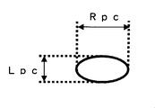
図2A〜図2Gに示したように、各凹部の開口を水平方向に投影した得られた直線のうち、最小となる直線の長さを短軸径と定義し、最大となる直線の長さを長軸径と定義する。例えば、円の場合は直径、楕円の場合は短径、長方形の場合は辺のうち短い方を短軸径として採用する。また、例えば、円の場合は直径、楕円の場合は長径、四角形の場合は対角線のうち長い方を長軸径として採用する。 As shown in FIGS. 2A to 2G, among the straight lines obtained by projecting the openings of the recesses in the horizontal direction, the minimum straight line length is defined as the short axis diameter, and the maximum straight line length is defined. Is defined as the major axis diameter. For example, the diameter is adopted as the minor axis diameter in the case of a circle, the minor axis in the case of an ellipse, and the shorter one of the sides in the case of a rectangle. In addition, for example, the diameter is adopted as the major axis diameter in the case of a circle, the major axis in the case of an ellipse, and the longer one of diagonal lines in the case of a quadrangle.
短軸径および長軸径の測定において、例えば図3Cに示すように凹部と非凹部との境界が明瞭でない場合は、その断面形状を考慮し、凹部形成前の平滑面を基準として凹部の開口の形状を定め、上記と同様にして単軸径および長軸径を測定する。さらに、図3Fに示すように凹部形成前の平滑面が不明瞭である場合は、隣り合う凹部同志の断面図において中心線を設け、短軸径及び長軸径を測定する。測定は対象となる感光体の表面を感光体回転方向に4等分し、該感光体回転方向と直交する方向に25等分して得られる計100箇所の領域のそれぞれの中に、一辺100μmの正方形の領域を設け、その正方形の中に含まれる凹部について行う。このようにして得られた単位面積当たりの凹部の各々の短軸径・長軸径を統計処理し、その平均値を平均短軸径・平均長軸径と定義する。本明細書において、長軸径および平均長軸径は共に符号Rpcによって表され、短軸径および平均短軸径は共に符号Lpcによって表される。 In the measurement of the short axis diameter and the long axis diameter, for example, as shown in FIG. 3C, when the boundary between the recess and the non-recess is not clear, the cross-sectional shape is taken into consideration, and the recess opening is defined with reference to the smooth surface before the recess is formed. And determine the uniaxial diameter and the major axis diameter in the same manner as described above. Further, as shown in FIG. 3F, when the smooth surface before the formation of the recess is unclear, a center line is provided in the cross-sectional view of the adjacent recesses, and the minor axis diameter and the major axis diameter are measured. In the measurement, the surface of the target photoconductor is divided into four equal parts in the rotation direction of the photoconductor, and divided into 25 equal parts in the direction orthogonal to the rotation direction of the photoconductor, and each of 100 regions is obtained. A square region is provided, and the recesses included in the square are performed. The short axis diameter and the long axis diameter of each of the concave portions per unit area thus obtained are statistically processed, and the average value is defined as the average short axis diameter and the average long axis diameter. In this specification, the major axis diameter and the average major axis diameter are both represented by the symbol Rpc, and the minor axis diameter and the average minor axis diameter are both represented by the symbol Lpc.
本発明における電子写真感光体の特徴の一つは、すでにWO2005−093518号公報において開示した電子写真感光体において、そのディンプル形状の凹部をより微細に形成したことである。このことにより、クリーニングブレードとの摩擦抵抗自体が格段に減少し、結果としてクリーニング性能が向上するが、この際、Lpc<Dtとすることにより転写効率が向上し、クリーニング性がさらに向上することを見出した。さらには、Lpc<Dt−σであることがより好ましい(Dt−σは、Dtからトナーの粒度分布の標準偏差を引いた値を表す)。これは凹部を有する電子写真感光体において、Lpc<Dtとすることにより、感光体に対するトナーの接触面積を減少させることが出来るためだと考えられる。 One of the features of the electrophotographic photosensitive member in the present invention is that the dimple-shaped concave portion is formed more finely in the electrophotographic photosensitive member already disclosed in WO2005-093518. As a result, the frictional resistance with the cleaning blade itself is remarkably reduced, and as a result, the cleaning performance is improved. At this time, by setting Lpc <Dt, the transfer efficiency is improved and the cleaning property is further improved. I found it. Further, it is more preferable that Lpc <Dt− σ (Dt− σ represents a value obtained by subtracting the standard deviation of the toner particle size distribution from Dt). This is considered to be because, in an electrophotographic photosensitive member having a concave portion, the contact area of the toner with respect to the photosensitive member can be reduced by setting Lpc <Dt.
また、この時Dg<Lpcとすることにより、耐久使用時における耐トナーフィルミング性が良好に維持でき、クリーニング性能がより一層向上できることを見出した。 Further, it was found that by setting Dg <Lpc at this time, the toner filming resistance during durable use can be maintained well, and the cleaning performance can be further improved.
一般に良好なクリーニング性能とは、転写されずに感光体の表面に残存するトナー粒子および外添材がクリーニングブレードと電子写真感光体の間に介在することにより発現されている状態であると考えられている。すなわち、従来技術においては、転写されずに残ったトナーの一部を利用することによりクリーニング性能を発揮していると考えられる。、クリーニングブレードと電子写真感光体の間に介在するトナー量が適当な範囲にないと、場合によっては残存するトナーとの摩擦抵抗の増大に起因する融着などの問題が発生することがある。より具体的には、転写されずに残ったトナーが十分に多い場合には、良好なクリーニング性能が発現されていたが、転写効率が高い場合、印字濃度の薄いパターンの大量印刷時およびタンデム形式の電子写真システムにおいての単色連続印刷時には、クリーニングブレードエッジに介在するトナーが極端に少なくなるため、クリーニングブレードと電子写真感光体との摩擦抵抗が増大しやすく、結果としてトナーが融着しやすい傾向にある。 In general, good cleaning performance is considered to be a state where toner particles and external additives remaining on the surface of the photoconductor without being transferred are expressed between the cleaning blade and the electrophotographic photoconductor. ing. That is, in the prior art, it is considered that the cleaning performance is exhibited by utilizing a part of the toner remaining without being transferred. If the amount of toner interposed between the cleaning blade and the electrophotographic photosensitive member is not within an appropriate range, problems such as fusion due to an increase in frictional resistance with the remaining toner may occur in some cases. More specifically, when the toner remaining without being transferred is sufficiently large, good cleaning performance was exhibited, but when the transfer efficiency is high, when printing a large amount of a pattern with a low print density and in tandem format During continuous monochrome printing in this electrophotographic system, the amount of toner intervening at the edge of the cleaning blade is extremely small, so the frictional resistance between the cleaning blade and the electrophotographic photosensitive member tends to increase, and as a result, the toner tends to be fused. It is in.
これに対して、本発明に係わる電子写真感光体は後述するようにトナーの転写効率が非常に高いため、従来技術のようにクリーニングに関わる現像材の効果を利用できにくい傾向にある。しかしながら、電子写真感光体とクリーニングブレードとの摩擦係数が格段に小さいことにより、トナーの量が少量でも、良好なクリーニング性能が保持されているものと考えられる。また、Dg<Lpcとすることによりディンプルの内部に、外添材を効率よく保持できることが、良好なクリーニング性能に寄与していると考えられる。 On the other hand, since the electrophotographic photosensitive member according to the present invention has a very high toner transfer efficiency as will be described later, it tends to be difficult to use the effect of the developer related to cleaning as in the prior art. However, since the friction coefficient between the electrophotographic photosensitive member and the cleaning blade is remarkably small, it is considered that good cleaning performance is maintained even with a small amount of toner. Further, it can be considered that the fact that the external additive can be efficiently held inside the dimple by making Dg <Lpc contributes to good cleaning performance.
従って本発明の画像形成方法によれば、印字濃度の薄い大量印刷時およびタンデム形式の電子写真システムにおいての単色連続印刷時などにおいてもクリーニングにおける不具合が生じにくい傾向にある。 Therefore, according to the image forming method of the present invention, there is a tendency that problems in cleaning are less likely to occur even when printing a large amount of light with a low print density or when performing monochromatic continuous printing in a tandem type electrophotographic system.
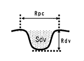
凹部の形状の具体例を図2A〜図2Gおよび図3A〜図3Fに示す。これらのうち、図4Aおよび図4Bに示したように、凹部の開口の長軸径を含み感光体の回転軸に垂直なディンプルの断面において、長軸径をRpc、深さをRdvとしたとき、その断面積SdvがSdv<Rdv×Rpcの関係を満たすディンプル形状が好ましい。より具体的には、基準面でのディンプル径に対して深さ方向にディンプル径が小さくなる形状が好ましい。また、ディンプル形成前の平滑面(基準面)とディンプルが明確な境界線を持たない、連続した曲面で形成されることがより好ましい。このような形状を有することによって、クリーニングブレードと電子写真感光体表面との接触がよりスムーズになり、良好なクリーニング性能が発揮されやすい。また、ドット再現性の点で(1/2)×Rdv×Rpc<Sdvであることが好ましい。 Specific examples of the shape of the recess are shown in FIGS. 2A to 2G and FIGS. 3A to 3F. Of these, as shown in FIGS. 4A and 4B, when the major axis diameter is Rpc and the depth is Rdv in the cross section of the dimple that includes the major axis diameter of the opening of the recess and is perpendicular to the rotation axis of the photoreceptor. A dimple shape whose cross-sectional area Sdv satisfies the relationship of Sdv <Rdv × Rpc is preferable. More specifically, a shape in which the dimple diameter is smaller in the depth direction than the dimple diameter on the reference plane is preferable. Further, it is more preferable that the smooth surface (reference surface) before the dimple formation and the dimple are formed by a continuous curved surface having no clear boundary line. By having such a shape, contact between the cleaning blade and the electrophotographic photosensitive member surface becomes smoother, and good cleaning performance is easily exhibited. In terms of dot reproducibility, it is preferable that (1/2) × Rdv × Rpc <Sdv.
さらに、ディンプルの開口の合計面積が、電子写真感光体表面全体の面積に対して40%以上であることが好ましく、61%以上であることがより好ましい。ディンプル形状の凹部の合計面積が小さすぎると本発明の効果が得られにくくなる。 Further, the total area of the dimple openings is preferably 40% or more, and more preferably 61% or more with respect to the entire surface area of the electrophotographic photosensitive member. If the total area of the dimple-shaped recesses is too small, it is difficult to obtain the effects of the present invention.
画像流れ(スジ状の画像欠陥)の防止のためには、すでにWO2005−093518号公報において開示したように、ディンプルが、それぞれ孤立し、特にディンプル形状の凹部が電子写真感光体の周方向や母線方向(回転軸方向)に連なってスジ状になっていないことが好ましい点では共通している。これに対しても、本発明に係わる電子写真感光体においては、さらにディンプルの大きさが潜像スポット径に対して格段に小さくなったことにより、より微細な文字などのドット再現性が向上する。 In order to prevent image flow (streak-like image defects), as already disclosed in WO 2005-093518, the dimples are isolated from each other, and particularly the dimple-shaped recesses are formed in the circumferential direction of the electrophotographic photosensitive member or the bus bar. It is common in the point that it is preferable that it does not become a streak line in a row (direction of rotation axis). In contrast, in the electrophotographic photosensitive member according to the present invention, the reproducibility of finer characters and the like is further improved by further reducing the size of the dimples relative to the latent image spot diameter. .
本発明において、電子写真感光体の表面のディンプル形状の凹部の測定は、市販のレーザー顕微鏡により可能である。例えば、(株)キーエンス製の超深度形状測定顕微鏡VK−8550、VK−8700、(株)菱化システム製の表面形状測定システムSurface Explorer SX−520DR型機、オリンパス(株)製の走査型共焦点レーザー顕微鏡OLS3000、レーザーテック(株)製のリアルカラーコンフォーカル顕微鏡オプリテクスC130が利用可能である。これらのレーザー顕微鏡を用いて、所定の倍率によりある視野におけるディンプルの開口の短軸径Lpc、ディンプルの開口の長軸径Rpcまたは最長径Epc(後述)、およびディンプルの深さRdvおよび断面積Sdvを計測することができる。さらには、単位面積あたりのディンプルの開口の面積率を計算により求めることができる。 In the present invention, the measurement of the dimple-shaped depressions on the surface of the electrophotographic photosensitive member can be performed with a commercially available laser microscope. For example, ultra deep depth measurement microscopes VK-8550 and VK-8700 manufactured by Keyence Co., Ltd., surface shape measurement system Surface Explorer SX-520DR model manufactured by Ryoka System Co., Ltd., and scanning type manufactured by Olympus Co., Ltd. A focus laser microscope OLS3000 and a real color confocal microscope Oplitex C130 manufactured by Lasertec Corporation can be used. Using these laser microscopes, the short axis diameter Lpc of the dimple opening, the long axis diameter Rpc or longest diameter Epc (described later) of the dimple opening, and the dimple depth Rdv and the cross-sectional area Sdv at a predetermined field of view using these laser microscopes. Can be measured. Furthermore, the area ratio of the dimple opening per unit area can be obtained by calculation.
一例として、Surface Explorer SX−520DR型機による解析プログラムを利用した測定例について説明する。測定対象の電子写真感光体をワーク置き台に設置し、チルト調整して水平を合わせ、ウエーブモードで電子写真感光体の周面の3次元形状データを取り込んだ。その際、対物レンズの倍率を50倍とし、100μm×100μm(10000μm2)の視野観察としてもよい。この方法で、測定対象の感光体の表面を感光体回転方向に4等分し、該感光体回転方向と直交する方向に25等分して得られる計100箇所の領域のそれぞれの中に、一辺100μmの正方形の領域を設けて測定する。 As an example, a measurement example using an analysis program by the Surface Explorer SX-520DR type machine will be described. The electrophotographic photosensitive member to be measured was placed on the work table, and the tilt was adjusted to adjust the horizontal, and the three-dimensional shape data of the peripheral surface of the electrophotographic photosensitive member was captured in the wave mode. At that time, the magnification of the objective lens may be 50 times, and the field of view may be 100 μm × 100 μm (10000 μm 2 ). In this method, the surface of the photoconductor to be measured is divided into four equal parts in the direction of rotation of the photoconductor and divided into 25 equal parts in a direction perpendicular to the direction of rotation of the photoconductor, Measurement is performed by providing a square region having a side of 100 μm.
次に、データ解析ソフト中の粒子解析プログラムを用いて電子写真感光体の表面の等高線データを表示する。
凹部の形状、長軸径、深さおよび開口面積のような凹部の孔解析パラメーターは、形成されたディンプルによって各々最適化することができるが、例えば最長径10μm程度のディンプルの観察および測定を行う場合、最長径上限を15μm、最長径下限を1μm、深さ下限を0.1μm、体積下限を1μm3とした。そして、解析画面上でディンプル形状と判別できる凹部の個数をカウントし、これを凹部の個数とした。
Next, the contour line data of the surface of the electrophotographic photosensitive member is displayed using a particle analysis program in the data analysis software.
The hole analysis parameters of the recess, such as the shape of the recess, the major axis diameter, the depth, and the opening area, can be optimized by the formed dimples. For example, a dimple having a longest diameter of about 10 μm is observed and measured. In this case, the upper limit of the longest diameter was 15 μm, the lower limit of the longest diameter was 1 μm, the lower limit of depth was 0.1 μm, and the lower limit of volume was 1 μm 3 . Then, the number of recesses that can be distinguished from the dimple shape on the analysis screen was counted, and this was used as the number of recesses.
また、上記と同様の視野および解析条件で、上記粒子解析プログラムを用いて求められる各ディンプルの開口の面積のから凹部の合計開口面積を算出し、下記式
(凹部の合計開口面積/総面積)×100(%)
から凹部の開口面積率を算出した。(以下、単に面積率と表記したものは、この開口面積率を示す)
In addition, the total opening area of the recess is calculated from the area of the opening of each dimple obtained using the particle analysis program under the same field of view and analysis conditions as above, and the following formula (total opening area / total area of the recess) × 100 (%)
From this, the opening area ratio of the recesses was calculated. (Hereinafter, what is simply expressed as area ratio indicates this opening area ratio)
なお、開口の長軸径が1μm程度以下の凹部については、レーザー顕微鏡および光学顕微鏡による観察が可能であるが、より測定精度を高める場合には、(株)キーエンス製の超深度形状測定顕微鏡VK−9500、VK−9500GII、VK−9700、(株)島津製作所製のナノサーチ顕微鏡SFT−3500の如きバイオレットレーザー顕微鏡、あるいは(株)キーエンス製のリアルサーフェスビュー顕微鏡VE−7800、VE−8800、VE−9800、日本電子(株)製のキャリースコープJCM−5100の如き電子顕微鏡による観察および測定を行うことが好ましい。 In addition, about the recessed part whose major axis diameter of an opening is about 1 micrometer or less, although observation with a laser microscope and an optical microscope is possible, in order to raise a measurement precision further, the ultra deep shape measuring microscope VK made from Keyence Corporation. -9500, VK-9500GII, VK-9700, Violet laser microscope such as Nano Search Microscope SFT-3500 manufactured by Shimadzu Corporation, or Real Surface View Microscope VE-7800, VE-8800, VE manufactured by Keyence Corporation It is preferable to perform observation and measurement with an electron microscope such as -9800, carry scope JCM-5100 manufactured by JEOL Ltd.
さて、本発明において、電子写真感光体の表面にディンプル形状の凹部を複数形成する方法して、例えば、レーザーアブレーション加工が挙げられる。レーザーアブレーション加工により、感光体表面にディンプル形状の凹部を形成する場合、用いるレーザーの発振パルス幅が、1ps以上100ns以下であることが好ましい。発振パルス幅が1psより短い場合は、基準面のディンプル径に対して深さ方向にディンプル径が小さくなる形状が得られにくくなり、生産コストも高くなる。また発振パルス幅が100nsより長い場合は、熱による表面ダメージを受けやすくなり、所望の径のディンプルが得られにくくなる。発振パルス幅が、1ps以上100ns以下であるレーザーとしては、エキシマーレーザーが好適に利用できる。 In the present invention, a method for forming a plurality of dimple-shaped recesses on the surface of the electrophotographic photosensitive member includes, for example, laser ablation. When a dimple-shaped recess is formed on the surface of the photoreceptor by laser ablation processing, it is preferable that the oscillation pulse width of the laser to be used is 1 ps or more and 100 ns or less. When the oscillation pulse width is shorter than 1 ps, it becomes difficult to obtain a shape in which the dimple diameter decreases in the depth direction with respect to the dimple diameter of the reference plane, and the production cost increases. Further, when the oscillation pulse width is longer than 100 ns, surface damage due to heat is likely to occur, and it becomes difficult to obtain dimples having a desired diameter. As the laser having an oscillation pulse width of 1 ps or more and 100 ns or less, an excimer laser can be suitably used.
本発明で用いるエキシマレーザーは、Ar、Kr、Xeの如き希ガスとF、Clの如きハロゲンガスの混合気体を放電、電子ビーム又は、X線でエネルギーを与えて励起して結合した後、基底状態に落ちることで解離する際にレーザー光を放出するものである。 The excimer laser used in the present invention is a mixture of a rare gas such as Ar, Kr and Xe and a halogen gas such as F and Cl excited by applying energy by discharge, electron beam or X-ray, Laser light is emitted when dissociated by falling into a state.
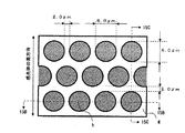
エキシマレーザーにおいて用いるガスとしては、ArF、KrF、XeCl、XeFが挙げられる。特にKrF又はArFが好ましい。凹部の形成方法としては、図5に示すような、レーザー光透過部bと遮蔽部aを適宣配列したマスクを使用する。マスクを透過したレーザー光のみがレンズで集光され、被加工物に照射されることにより、所望の形状と配列を有した凹部の形成が可能となる。一定面積内の多数の凹部を、凹部の形状、面積に関わらず瞬時に同時に形成できるため、工程は短時間ですむ。図6においてマスクを用いたレーザー照射は、エキシマレーザー光照射器cで1回照射あたり数mm2から数cm2の加工が為される。レーザー加工においては、図6に示すように、感光体(例えば、感光ドラム)fをワーク回転用モーターdで自転させつつ、レーザー照射位置をワーク移動装置eで感光体の軸方向上にずらしていくことにより、感光体の表面全域に効率良く凹部を形成することができる。凹部の深さは0.1〜2.0μmとすることが好ましい。本発明によれば、凹部の大きさ、形状、配列の制御性が高く、高精度かつ自由度の高い粗面加工が実現できる。 Examples of the gas used in the excimer laser include ArF, KrF, XeCl, and XeF. Particularly preferred is KrF or ArF. As a method for forming the recess, a mask in which a laser beam transmitting part b and a shielding part a are appropriately arranged as shown in FIG. 5 is used. Only laser light that has passed through the mask is condensed by the lens and irradiated onto the workpiece, so that a recess having a desired shape and arrangement can be formed. Since a large number of recesses within a certain area can be simultaneously formed regardless of the shape and area of the recesses, the process can be completed in a short time. In the laser irradiation using the mask in FIG. 6, processing of several mm 2 to several cm 2 is performed per irradiation with the excimer laser beam irradiator c. In laser processing, as shown in FIG. 6, a photosensitive member (for example, a photosensitive drum) f is rotated by a workpiece rotating motor d, and the laser irradiation position is shifted on the axial direction of the photosensitive member by a workpiece moving device e. Accordingly, the concave portions can be efficiently formed in the entire surface of the photoreceptor. The depth of the recess is preferably 0.1 to 2.0 μm. According to the present invention, it is possible to realize rough surface processing with high controllability of the size, shape, and arrangement of the recesses, and with high accuracy and high flexibility.
また、本発明において、同じマスクパターンの繰返し加工を採用した場合、感光体表面全体における粗面均一性が高くなり、その結果、電子写真装置において使用する際のクリーニングブレードにかかる力学的負荷は均一となる。また、図7に示すように、感光体の任意の周方向線上に、凹部形成部hと凹部非形成部gの双方が存在する配列となるようにマスクパターンを形成することにより、クリーニングブレードにかかる力学的負荷の偏在は一層防止できる。 Further, in the present invention, when the same mask pattern is repeatedly processed, the uniformity of the rough surface on the entire surface of the photoreceptor is increased, and as a result, the mechanical load applied to the cleaning blade when used in the electrophotographic apparatus is uniform. It becomes. Further, as shown in FIG. 7, a mask pattern is formed on an arbitrary circumferential line of the photosensitive member so that both of the concave portion forming portion h and the concave portion non-forming portion g are arranged, thereby forming a cleaning blade. Such uneven distribution of mechanical load can be further prevented.
また、本発明において、電子写真感光体の表面にディンプル形状の凹部を複数形成する別の方法として、所定の形状を有するモールドを電子写真感光体の表面に圧接して形状転写を行う方法が挙げられる。 In the present invention, another method for forming a plurality of dimple-shaped recesses on the surface of the electrophotographic photosensitive member is a method of performing shape transfer by pressing a mold having a predetermined shape against the surface of the electrophotographic photosensitive member. It is done.
図8に装置の断面の概略図を示す。加圧および解除が繰り返し行える加圧装置Aに所定のモールドBを取り付けた後、感光体Cに対して所定の圧力でモールドを当接させて形状転写を行う。その後加圧を一旦解除し、感光体を回転させた後に、再度加圧して形状転写工程を行う。この工程を繰り返すことにより、感光体の全周にわたって所定のディンプル形状を形成することが可能である。 FIG. 8 shows a schematic diagram of a cross section of the apparatus. After the predetermined mold B is attached to the pressure device A that can repeatedly press and release, the mold is brought into contact with the photoreceptor C at a predetermined pressure to transfer the shape. Thereafter, the pressure is once released and the photosensitive member is rotated, and then the pressure is again applied to perform the shape transfer process. By repeating this process, it is possible to form a predetermined dimple shape over the entire circumference of the photoreceptor.
また、図9に示したように、加圧装置Aに感光体の全周長よりも長いモールドBを取り付けた後、感光体Cに対して所定の圧力をかけながら、感光体を矢印の方向に回転、移動させることにより、感光体全周にわたって所定のディンプル形状を形成することも可能である。 Further, as shown in FIG. 9, after the mold B longer than the entire circumference of the photoconductor is attached to the pressure device A, the photoconductor is moved in the direction of the arrow while applying a predetermined pressure to the photoconductor C. It is also possible to form a predetermined dimple shape over the entire circumference of the photoconductor by rotating and moving the photoconductor.
他の例として、シート状のモールドをロール状の加圧装置と感光体の間に挟み、モールドシートを送りながら表面加工することも可能である。なお、形状転写を効率的に行う目的で、モールドや感光体を加熱することも可能である。 As another example, a sheet-shaped mold may be sandwiched between a roll-shaped pressurizing device and a photoreceptor, and surface processing may be performed while feeding the mold sheet. It is also possible to heat the mold and the photoreceptor for the purpose of efficiently transferring the shape.
モールド自体の材質や大きさ、形状は適宜選択することができる。材質としては、微細表面加工された金属、又はシリコンウエハーの表面にレジストによりパターンニングをしたもの、微粒子が分散された樹脂フィルム、所定の微細表面形状を有する樹脂フィルムに金属コーティングされたものが挙げられる。モールド形状の一例を図10Aおよび図10Bに示す。図10Aにおいて、10A−1はモールド形状を上方向から見た図であり、10A−2はモールド形状を横方向から見た図である。図10Bにおいて、10B−1はモールド形状を上方向から見た図であり、10B−2はモールド形状を横方向から見た図である。
また、感光体に対して圧力を均一に付与する目的で、モールドと加圧装置の間に弾性体を設置することも可能である。
The material, size, and shape of the mold itself can be selected as appropriate. Examples of the material include a metal having a fine surface processed, or a silicon wafer surface patterned with a resist, a resin film in which fine particles are dispersed, and a metal film coated on a resin film having a predetermined fine surface shape. It is done. An example of the mold shape is shown in FIGS. 10A and 10B. In FIG. 10A, 10A-1 is the figure which looked at the mold shape from the upper direction, and 10A-2 is the figure which looked at the mold shape from the horizontal direction. In FIG. 10B, 10B-1 is the figure which looked at the mold shape from the upper direction, and 10B-2 is the figure which looked at the mold shape from the horizontal direction.
It is also possible to install an elastic body between the mold and the pressure device for the purpose of uniformly applying pressure to the photoreceptor.
本発明において無機微粉体の平均粒径の測定は、走査型電子顕微鏡FE−SEM(日立製作所製S−4700)により50万倍に拡大したトナー粒子の表面の写真を撮影し、その拡大写真を測定対象として行う。一次粒子の平均粒径は、拡大写真において10視野にわたり測定し、その平均を平均粒径とする。なお、無機微粉体の一次粒子の輪郭に接する様に引いた平行線の内、その平行線間距離が最大となるものを粒径とする。 In the present invention, the average particle size of the inorganic fine powder is measured by taking a photograph of the surface of the toner particles magnified 500,000 times with a scanning electron microscope FE-SEM (S-4700, manufactured by Hitachi, Ltd.). Perform as a measurement target. The average particle diameter of primary particles is measured over 10 fields in an enlarged photograph, and the average is defined as the average particle diameter. Of the parallel lines drawn so as to be in contact with the contours of the primary particles of the inorganic fine powder, the particle diameter having the maximum distance between the parallel lines is defined as the particle size.
拡大写真から粒径0.001μm以上の粒子をランダムに500個以上抽出し、一次粒子の輪郭に接する様に引いた平行線の内、その平行線間距離が最大となるものを粒径とする。500個以上の粒子の粒径分布のピークになる粒径をもって個数平均粒径を算出する。 500 or more particles with a particle size of 0.001 μm or more are randomly extracted from the enlarged photograph, and among the parallel lines drawn so as to be in contact with the outline of the primary particles, the particle having the maximum distance between the parallel lines is defined as the particle size. . The number average particle size is calculated with the particle size that becomes the peak of the particle size distribution of 500 or more particles.
ピークが単独である場合は、ピークとなる粒径値を、無機微粉体の個数平均粒径の最大値とし、ピークが複数ある場合は、このうち最大のピーク値を、無機微粉体の個数平均粒径とする。 When there is a single peak, the peak particle size value is the maximum value of the number average particle size of the inorganic fine powder, and when there are multiple peaks, the maximum peak value is the number average of the inorganic fine powder. The particle size.
トナーの重量平均粒径は、細孔電気抵抗法によって好適に測定できる。本発明においてトナーの重量平均粒径の測定は、コールターマルチサイザーII(コールター社製)を用いる。電解液は1級塩化ナトリウムを用いて調製した1%NaCl水溶液を用いればよく、例えば、ISOTON R−II(コールターサイエンティフィックジャパン社製)が使用できる。測定法としては、前記電解水溶液100−150ml中に分散剤として界面活性剤(好ましくはアルキルベンゼンスルホン酸塩)を0.3ml加え、更に測定試料を2〜20mg加える。試料を懸濁した電解液は超音波分散器で約1〜3分間分散処理を行い、前記測定装置によりトナーの体積、個数を測定して体積分布と個数分布とを算出し、重量平均粒径(D4)(各チャンネルの中央値をチャンネル毎の代表値とする)及びその標準偏差を求める。 The weight average particle diameter of the toner can be suitably measured by a pore electrical resistance method. In the present invention, the weight average particle diameter of the toner is measured using Coulter Multisizer II (manufactured by Coulter). As the electrolytic solution, a 1% NaCl aqueous solution prepared using primary sodium chloride may be used. For example, ISOTON R-II (manufactured by Coulter Scientific Japan) may be used. As a measuring method, 0.3 ml of a surfactant (preferably alkylbenzene sulfonate) is added as a dispersant to 100 to 150 ml of the electrolytic aqueous solution, and 2 to 20 mg of a measurement sample is further added. The electrolyte in which the sample is suspended is subjected to a dispersion treatment with an ultrasonic disperser for about 1 to 3 minutes, and the volume and number distribution of the toner are measured by the measuring device to calculate the volume distribution and the number distribution. (D4) (The median value of each channel is used as a representative value for each channel) and its standard deviation are obtained.
重量平均粒径が、6.0μmより大きい場合には、100μmアパーチャーを用いて、2〜60μmの粒子を測定し、重量平均粒径3.0〜6.0μmの場合には、50μmアパーチャーを用い、1〜30μmの粒子を測定し、重量平均粒径が3.0μm未満の場合には、30μmアパーチャーを用い、0.6〜18μmの粒子を測定する。 When the weight average particle size is larger than 6.0 μm, the particle size of 2 to 60 μm is measured using a 100 μm aperture, and when the weight average particle size is 3.0 to 6.0 μm, the 50 μm aperture is used. 1 to 30 μm particles are measured, and when the weight average particle diameter is less than 3.0 μm, particles of 0.6 to 18 μm are measured using a 30 μm aperture.
本発明において、トナーの形状は、平均円形度および形状係数にて定義される。
トナーの平均円形度は、フロー式粒子像測定装置「FPIA−2100型」(シスメックス社製)を用いて測定を行い、下式を用いて算出する。

The average circularity of the toner is measured using a flow type particle image measuring device “FPIA-2100 type” (manufactured by Sysmex Corporation), and is calculated using the following equation.
本発明における円形度はトナー粒子の凹凸の度合いを示す指標であり、トナー粒子が完全な球形の場合に1.000を示し、表面形状が複雑になる程、円形度は小さな値となる。 In the present invention, the circularity is an index indicating the degree of unevenness of the toner particles, and is 1.000 when the toner particles are completely spherical. The more complicated the surface shape, the smaller the circularity.
また、円形度頻度分布の平均値を意味する平均円形度Cは、粒度分布の分割点iでの円形度(中心値)をci、測定粒子数をmとすると、次式から算出される。
なお、本発明で用いている測定装置である「FPIA−2100」は、各粒子の円形度を算出後、平均円形度の算出に当たって、得られた円形度によって、粒子を円形度0.4〜1.0を0.01ごとに等分割したクラスに分け、その分割点の中心値と測定粒子数を用いて平均円形度の算出を行う。 In addition, “FPIA-2100”, which is a measuring apparatus used in the present invention, calculates the circularity of each particle, and then calculates the average circularity. 1.0 is divided into classes equally divided every 0.01, and the average circularity is calculated using the center value of the division points and the number of measured particles.
具体的な測定方法としては、容器中に予め不純固形物などを除去したイオン交換水10mlを用意し、その中に分散剤として界面活性剤、好ましくはアルキルベンゼンスルホン酸塩を加えた後、更に測定試料を0.02g加え、均一に分散させる。分散させる手段としては、超音波分散機「Tetora150型」(日科機バイオス社製)を用い、2分間分散処理を行い、測定用の分散液とする。その際、該分散液の温度が40℃以上とならない様に適宜冷却する。また、円形度のバラツキを抑えるため、フロー式粒子像分析装置FPIA−2100の機内温度が26〜27℃になるように装置の設置環境を23℃±0.5℃にコントロールし、一定時間おきに、好ましくは2時間おきに2μmラテックス粒子を用いて自動焦点調整を行う。
As a specific measuring method, 10 ml of ion-exchanged water from which impure solids have been removed in advance is prepared in a container, and a surfactant, preferably an alkylbenzene sulfonate, is added as a dispersant therein, followed by further measurement. Add 0.02 g of sample and disperse uniformly. As a means for dispersion, an ultrasonic disperser “
トナーの円形度測定には、前記フロー式粒子像測定装置を用い、測定時のトナーの濃度が3000〜1万個/μlとなる様に該分散液濃度を再調整し、トナーの粒子を1000個以上計測する。計測後、このデータを用いて、円相当径2μm未満のデータをカットして、トナーの平均円形度を求める。 For measuring the circularity of the toner, the flow type particle image measuring device is used, and the concentration of the dispersion is readjusted so that the concentration of the toner at the time of measurement is 3000 to 10,000 / μl. Measure more than one. After the measurement, data having an equivalent circle diameter of less than 2 μm is cut using this data to obtain the average circularity of the toner.
さらに、本発明で用いている測定装置である「FPIA−2100」は、従来よりトナーの形状を算出するために用いられていた「FPIA−1000」と比較して、処理粒子画像の倍率の向上、さらに取り込んだ画像の処理解像度の向上(256×256→512×512)によりトナーの形状測定の精度が上がっており、それにより微粒子のより確実な補足を達成している装置である。従って、本発明のように、より正確に形状を測定する必要がある場合には、より正確に形状に関する情報が得られるFPIA2100の方が有利である。 Furthermore, “FPIA-2100”, which is a measuring apparatus used in the present invention, improves the magnification of the processed particle image as compared with “FPIA-1000” conventionally used for calculating the shape of the toner. Further, the accuracy of toner shape measurement has been improved by improving the processing resolution of the captured image (256 × 256 → 512 × 512), thereby achieving more reliable capture of fine particles. Therefore, when it is necessary to measure the shape more accurately as in the present invention, the FPIA 2100 that can obtain information on the shape more accurately is advantageous.
トナー粒子の平均円形度は、0.925以上0.995以下であることが好ましい。平均円形度が0.925未満では、転写効率(特に多重転写や二次転写)が低下し始め、結果として耐久時のトナーフィルミング確立が上昇してしまう。逆に0.995を超えると、トナー自身が非常に良く転がるためクリーニングでのすり抜けが発生しやすくなり、結果としてクリーニング不良をおこしやすい。
The average circularity of the toner particles is preferably 0.925 or more and 0.995 or less . If the average circularity is less than 0.925, transfer efficiency (particularly multiple transfer and secondary transfer) starts to decrease, and as a result, the establishment of toner filming during durability increases. On the other hand, if it exceeds 0.995, the toner itself rolls very well, and slipping through cleaning is likely to occur, resulting in poor cleaning.
一方、トナーの形状係数は、例えば日立製作所製FE−SEM(S−4700又は4800)を用い、1000倍に拡大した2μm以上のトナー粒子像を100個無作為にサンプリングし、その画像情報はインターフェースを介して、例えばANALYSIS(soft imaging system Gmbh)に導入して解析を行い、下式より算出して得られた値を形状係数SF−1、SF−2と定義する。
なお、トナー粒子に外添剤を外添した後に、上記の方法によりトナーの形状係数の測定を行う場合には、トナー粒子の表面に付着している外添剤が画像解析データには含まれないようにして行った。 In the case where the shape factor of the toner is measured by the above method after the external additive is externally added to the toner particles, the external additive adhering to the surface of the toner particles is included in the image analysis data. I went so that there was no.
形状係数SF−1は粒子の全体的な丸さの度合いを示し、形状係数SF−2は粒子表面の微細な凹凸の度合いを示している。 The shape factor SF-1 indicates the degree of overall roundness of the particles, and the shape factor SF-2 indicates the degree of fine irregularities on the particle surface.
トナーの形状係数の比(SF−2)/(SF−1)は0.63以上1.00以下であることが好ましい。トナーの形状係数の比(SF−2)/(SF−1)の値が1.00を超えるときには、クリーニング不良が発生しやすく、トナーの形状係数SF−1が160を超えると、球形から離れて不定形に近づき、現像器内でトナーが破砕され易く、粒度分布が変動したり、帯電量分布がブロードになりやすくなるため、画像濃度低下や、地カブリや反転カブリといった画像カブリが生じやすい。また、SF−2が140を超えると、感光体から中間転写体及び転写材へのトナー像の転写効率の低下、および文字やライン画像の転写中抜けを招き好ましくない。 The toner shape factor ratio (SF-2) / (SF-1) is preferably 0.63 or more and 1.00 or less. When the toner shape factor ratio (SF-2) / (SF-1) exceeds 1.00, cleaning failure is likely to occur. When the toner shape factor SF-1 exceeds 160, the toner is separated from the spherical shape. The toner tends to be crushed in the developing unit, the particle size distribution fluctuates, and the charge amount distribution tends to become broad, so that image density decreases and image fogging such as background fogging and reversal fogging is likely to occur. . On the other hand, if SF-2 exceeds 140, the transfer efficiency of the toner image from the photosensitive member to the intermediate transfer member and the transfer material will be lowered, and the transfer of characters and line images may be lost.
また、トナーの平均円形度と感光体表面形状の関係において、
C≧−0.0241×Log(tan−1((Epc−Epch)/Edv))/Epc+0.917 ・・・数式2
(Epcは、各々独立した凹部の開口の感光体円周方向最長径を表し、
Edvは、該円周方向最長径を含み感光体の回転軸に垂直な凹部の断面における最大深さを表し、
Epchは、前記最大深さの半分の深さにおける、該凹部の感光体の円周方向の径
を示し、Cはトナーの平均円形度を示す)
であることが好ましい。C≦−0.0241×Log(tan−1((Epc−Epch)/Edv))/Epc+0.917の領域では、600dpiにて1ライン−1スペース画像を形成した場合等の高MTFチャート出力時において、潜像電荷密度の低い位置に対しても、現像ニップを通過する時にトナーが感光体の表面の凹部形状にトラップされてしまう傾向にあり、ライン再現性の低下をおこしやすい。
In addition, in the relationship between the average circularity of the toner and the surface shape of the photoreceptor,
C ≧ −0.0241 × Log (tan −1 ((Epc−Epch) / Edv)) / Epc + 0.917 Expression 2
(Epc represents the longest diameter in the circumferential direction of the photosensitive member in each independent recess opening,
Edv represents the maximum depth in the cross section of the concave portion including the longest diameter in the circumferential direction and perpendicular to the rotation axis of the photoconductor,
(Epch represents the diameter in the circumferential direction of the photoreceptor of the concave portion at half the maximum depth, and C represents the average circularity of the toner)
It is preferable that In the region of C ≦ −0.0241 × Log (tan −1 ((Epc−Epch) / Edv)) / Epc + 0.917, when a 1 line-1 space image is formed at 600 dpi, when outputting a high MTF chart, Even at a position where the latent image charge density is low, the toner tends to be trapped in the concave shape on the surface of the photosensitive member when passing through the development nip, and line reproducibility is liable to decrease.
本発明のトナーの製造方法は特に限定されないが、平均円形度を制御にするためには、懸濁重合法、機械式粉砕法、球形化処理によって製造されるのが好ましく、平均円形度0.925〜0.950とするためには機械式粉砕法、球形化処理が特に好ましく、平均円形度0.950〜0.995とするためには懸濁重合法が特に好ましい。
トナーの形状としては上記範囲にあることが好ましいが、この範囲は、上記トナーの粉砕条件や表面処理改質処理条件を調整することで達成できる。
The method for producing the toner of the present invention is not particularly limited, but in order to control the average circularity, the toner is preferably produced by a suspension polymerization method, a mechanical pulverization method, or a spheroidization treatment. In order to obtain 925 to 0.950, a mechanical pulverization method and a spheronization treatment are particularly preferred. In order to obtain an average circularity of 0.950 to 0.995, a suspension polymerization method is particularly preferred.
The toner shape is preferably in the above range, but this range can be achieved by adjusting the pulverization condition and surface treatment modification condition of the toner.
本発明は、表面が摩耗しにくい電子写真感光体を適用したときに最も効果的に作用する。表面が摩耗しにくい電子写真感光体は、高耐久である一方で、クリーニングブレードのビビリやメクレ、摺擦メモリー、画像流れ、現像性および転写性の問題が発生しやすい。 The present invention works most effectively when an electrophotographic photosensitive member whose surface is not easily worn is applied. An electrophotographic photosensitive member whose surface is not easily worn is highly durable, but is prone to problems of cleaning blade chatter, scratches, rubbing memory, image flow, developability and transferability.
本発明において、電子写真感光体の表面の弾性変形率は40%以上65%以下であることが好ましく、45%以上であることがより好ましく、50%以上であることがより一層好ましい。 In the present invention, the elastic deformation rate of the surface of the electrophotographic photosensitive member is preferably 40% or more and 65% or less, more preferably 45% or more, and even more preferably 50% or more.
また、電子写真感光体の表面のユニバーサル硬さ値(HU)は、150N/mm2以上220N/mm2以下であることが好ましい。 The universal hardness value (HU) of the surface of the electrophotographic photosensitive member is preferably 150 N / mm 2 or more and 220 N / mm 2 or less.
ユニバーサル硬さ値(HU)が大きすぎたり、また、弾性変形率が小さすぎると、電子写真感光体の表面の弾性力が不足しているため、電子写真感光体の周面とクリーニングブレードとの間に挟まれた紙粉やトナーが電子写真感光体の周面を擦ることによって、電子写真感光体の表面に傷が発生しやすくなり、それにともなって摩耗も発生しやすくなる。 If the universal hardness value (HU) is too large or the elastic deformation rate is too small, the elastic force on the surface of the electrophotographic photosensitive member is insufficient. The paper powder or toner sandwiched between the surfaces of the electrophotographic photosensitive member rubs against the surface of the electrophotographic photosensitive member, so that the surface of the electrophotographic photosensitive member is likely to be scratched.
また、ユニバーサル硬さ値(HU)が大きすぎると、たとえ弾性変形率が高くても弾性変形量は小さくなってしまうため、結果として電子写真感光体の表面の局部に大きな圧力がかかり、よって電子写真感光体の表面に深い傷が発生しやすくなる。 In addition, if the universal hardness value (HU) is too large, even if the elastic deformation rate is high, the amount of elastic deformation becomes small. As a result, a large pressure is applied to the local area of the surface of the electrophotographic photosensitive member, so that the electron Deep scratches are likely to occur on the surface of the photoconductor.
また、ユニバーサル硬さ値(HU)が上記範囲にあっても弾性変形率が小さすぎると、塑性変形量が相対的に大きくなってしまうため、電子写真感光体の表面に細かい傷が発生しやすくなり、また、摩耗も発生しやすくなる。これは、弾性変形率が小さすぎるだけでなくユニバーサル硬さ値(HU)が小さすぎる場合、特に顕著になる。 Further, even if the universal hardness value (HU) is in the above range, if the elastic deformation rate is too small, the amount of plastic deformation becomes relatively large, so that fine scratches are likely to occur on the surface of the electrophotographic photosensitive member. In addition, wear tends to occur. This is particularly noticeable not only when the elastic deformation rate is too small but also when the universal hardness value (HU) is too small.
以上のように表面が摩耗しにくく、さらに傷が発生しにくい電子写真感光体は、上記の微細表面形状が初期から繰り返し使用後まで変化が非常に小さく、あるいは変化しないため、長期間繰り返し使用した場合にも初期の性能を良好に維持することができる。 As described above, the electrophotographic photosensitive member whose surface is hard to be abraded and is less likely to be scratched is used repeatedly for a long time because the above-mentioned fine surface shape changes very little or does not change after the repeated use. Even in this case, the initial performance can be maintained well.
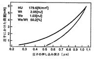
本発明において、電子写真感光体の表面のユニバーサル硬さ値(HU)および弾性変形率は、温度23℃/湿度50%RH環境下、微小硬さ測定装置フィシャースコープH100V(Fischer社製)を用いて測定した値である。このフィシャースコープH100Vは、測定対象(電子写真感光体の周面)に圧子を当接し、この圧子に連続的に荷重をかけ、荷重下での押し込み深さを直読することにより連続的硬さが求められる装置である。 In the present invention, for the universal hardness value (HU) and elastic deformation rate of the surface of the electrophotographic photosensitive member, a microhardness measuring device Fischerscope H100V (manufactured by Fischer) is used in an environment of temperature 23 ° C./humidity 50% RH. Measured value. The Fischerscope H100V has a continuous hardness by contacting an indenter with a measurement object (the peripheral surface of the electrophotographic photosensitive member), continuously applying a load to the indenter, and directly reading the indentation depth under the load. It is a required device.
本発明においては、圧子として対面角136°のビッカース四角錐ダイヤモンド圧子を用い、電子写真感光体の周面に圧子を押し当て、圧子に連続的にかける荷重の最終(最終荷重)を6mNとし、圧子に最終荷重6mNをかけた状態を保持する時間(保持時間)を0.1秒とした。また、測定点は273点とした。 In the present invention, a Vickers square pyramid diamond indenter with a facing angle of 136 ° is used as the indenter, the indenter is pressed against the peripheral surface of the electrophotographic photosensitive member, and the final load (final load) continuously applied to the indenter is 6 mN. The time (holding time) for holding the indenter with a final load of 6 mN was set to 0.1 second. The measurement points were 273 points.
フィシャースコープH100V(Fischer社製)の出力チャートの概略を図11に示す。また、本発明の電子写真感光体を測定対象としたときのフィシャースコープH100V(Fischer社製)の出力チャートの一例を図12に示す。図11及び図12中、縦軸は圧子にかけた荷重F(mN)を、横軸は圧子の押し込み深さh(μm)を示す。図11は、圧子にかける荷重を段階的に増加させて荷重が最大になった(A→B)後、段階的に荷重を減少させた(B→C)ときの結果を示している。図12は、圧子にかける荷重を段階的に増加させて最終的に荷重を6mNとし、その後、段階的に荷重を減少させたときの結果を示している。 An outline of the output chart of the Fischer scope H100V (Fischer) is shown in FIG. FIG. 12 shows an example of an output chart of the Fischer scope H100V (Fischer) when the electrophotographic photosensitive member of the present invention is used as a measurement target. 11 and 12, the vertical axis represents the load F (mN) applied to the indenter, and the horizontal axis represents the indentation depth h (μm). FIG. 11 shows the results when the load applied to the indenter is increased stepwise to maximize the load (A → B), and then the load is decreased stepwise (B → C). FIG. 12 shows the results when the load applied to the indenter is increased stepwise to finally set the load to 6 mN, and then the load is decreased stepwise.
ユニバーサル硬さ値(HU)は、圧子に最終荷重6mNをかけたときの該圧子の押し込み深さから下記式により求めることができる。なお、下記式中、HUはユニバーサル硬さ(HU)を意味し、Ffは最終荷重を意味し、Sfは最終荷重をかけたときの圧子の押し込まれた部分の表面積を意味し、hfは最終荷重をかけたときの圧子の押し込み深さを意味する。
また、弾性変形率は、圧子が測定対象(電子写真感光体の周面)に対して行った仕事量(エネルギー)、すなわち、圧子の測定対象(電子写真感光体の周面)に対する荷重の増減によるエネルギーの変化より求めることができる。具体的には、弾性変形仕事量Weを全仕事量Wtで除した値(We/Wt)が弾性変形率である。なお、全仕事量Wtは図11中のA−B−D−Aで囲まれる領域の面積であり、弾性変形仕事量Weは図11中のC−B−D−Cで囲まれる領域の面積である。 In addition, the elastic deformation rate is the work amount (energy) performed by the indenter on the measurement target (the peripheral surface of the electrophotographic photosensitive member), that is, the increase or decrease of the load on the measurement target of the indenter (the peripheral surface of the electrophotographic photosensitive member). It can be obtained from the change in energy due to. Specifically, a value (We / Wt) obtained by dividing the elastic deformation work We by the total work Wt is the elastic deformation rate. Note that the total work amount Wt is the area of the region surrounded by A-B-D-A in FIG. 11, and the elastic deformation work amount We is the area of the region surrounded by C-B-D-C in FIG. It is.
次に、本発明に係わる電子写真感光体の構成について説明する。
上述のとおり、本発明の電子写真感光体は、支持体および該支持体上に設けられた有機感光層(以下単に「感光層」ともいう。)を有する電子写真感光体である。一般的には、円筒状支持体上に感光層を形成した円筒状有機電子写真感光体が広く用いられるが、ベルト状あるいはシート状の形状も可能である。
Next, the configuration of the electrophotographic photosensitive member according to the present invention will be described.
As described above, the electrophotographic photosensitive member of the present invention is an electrophotographic photosensitive member having a support and an organic photosensitive layer (hereinafter also simply referred to as “photosensitive layer”) provided on the support. In general, a cylindrical organic electrophotographic photosensitive member having a photosensitive layer formed on a cylindrical support is widely used, but a belt-like or sheet-like shape is also possible.
感光層は、電荷輸送物質と電荷発生物質を同一の層に含有する単層型感光層であっても、電荷発生物質を含有する電荷発生層と電荷輸送物質を含有する電荷輸送層とに分離した積層型(機能分離型)感光層であってもよい。電子写真特性の観点からは、積層型感光層が好ましい。また、積層型感光層には、支持体側から電荷発生層、電荷輸送層の順に積層した順層型感光層と、支持体側から電荷輸送層、電荷発生層の順に積層した逆層型感光層がある。電子写真特性の観点からは順層型感光層が好ましい。また、電荷発生層を積層構造としてもよく、また、電荷輸送層を積層構成としてもよい。さらに、耐久性能向上を目的とし感光層上に保護層を設けることも可能である。 The photosensitive layer is separated into a charge generating layer containing a charge generating material and a charge transporting layer containing a charge transporting material even if it is a single layer type photosensitive layer containing the charge transporting material and the charge generating material in the same layer. The laminated (functional separation type) photosensitive layer may be used. From the viewpoint of electrophotographic characteristics, a laminated photosensitive layer is preferred. The laminated photosensitive layer has a normal layer type photosensitive layer laminated in the order of the charge generation layer and the charge transport layer from the support side, and a reverse layer type photosensitive layer laminated in the order of the charge transport layer and the charge generation layer from the support side. is there. From the viewpoint of electrophotographic characteristics, a normal layer type photosensitive layer is preferred. Further, the charge generation layer may have a laminated structure, and the charge transport layer may have a laminated structure. Further, a protective layer can be provided on the photosensitive layer for the purpose of improving the durability performance.
支持体としては、導電性を示すもの(導電性支持体)であればよく、鉄、銅、金、銀、アルミニウム、亜鉛、チタン、鉛、ニッケル、スズ、アンチモン、インジウム、クロム、アルミニウム合金、ステンレスの如き金属製(合金製)の支持体を用いることができる。また、アルミニウム、アルミニウム合金、酸化インジウム−酸化スズ合金を真空蒸着によって被膜形成した層を有する上記金属製支持体やプラスチック製支持体を用いることもできる。また、カーボンブラック、酸化スズ粒子、酸化チタン粒子、銀粒子の如き導電性粒子を適当な結着樹脂と共にプラスチックや紙に含浸した支持体や、導電性結着樹脂を有するプラスチック製の支持体を用いることもできる。 The support may be anything that exhibits conductivity (conductive support), such as iron, copper, gold, silver, aluminum, zinc, titanium, lead, nickel, tin, antimony, indium, chromium, aluminum alloy, A metal (alloy) support such as stainless steel can be used. Moreover, the said metal support body and plastic support body which have the layer which formed the film by vacuum deposition of aluminum, an aluminum alloy, and an indium oxide tin oxide alloy can also be used. Also, a support in which conductive particles such as carbon black, tin oxide particles, titanium oxide particles, and silver particles are impregnated into plastic or paper together with an appropriate binder resin, or a plastic support having a conductive binder resin is provided. It can also be used.
また、支持体の表面は、レーザー光の散乱による干渉縞の防止を目的として、切削処理、粗面化処理、又はアルマイト処理を施してもよい。 Further, the surface of the support may be subjected to a cutting process, a roughening process, or an alumite process for the purpose of preventing interference fringes due to scattering of laser light.
支持体と後述の中間層あるいは感光層(電荷発生層、電荷輸送層)との間には、レーザー光の散乱による干渉縞の防止や、支持体の傷の被覆を目的とした導電層を設けてもよい。 A conductive layer is provided between the support and the intermediate layer or photosensitive layer (charge generation layer, charge transport layer) described later for the purpose of preventing interference fringes due to laser light scattering and covering the scratches on the support. May be.
導電層は、カーボンブラック、導電性顔料や抵抗調節顔料を結着樹脂に分散および/または溶解させた導電層用塗布液を用いて形成することができる。導電層用塗布液には、加熱または放射線照射により硬化重合する化合物を添加してもよい。導電性顔料や抵抗調節顔料を分散させた導電層は、その表面が粗面化される傾向にある。 The conductive layer can be formed using a conductive layer coating solution in which carbon black, a conductive pigment or a resistance adjusting pigment is dispersed and / or dissolved in a binder resin. You may add the compound which carries out hardening polymerization by the heating or radiation irradiation to the coating liquid for conductive layers. The surface of a conductive layer in which a conductive pigment or a resistance adjusting pigment is dispersed tends to be roughened.
導電層の膜厚は、0.2〜40μmであることが好ましく、さらには1〜35μmであることがより好ましく、さらには5〜30μmであることがより一層好ましい。 The thickness of the conductive layer is preferably 0.2 to 40 μm, more preferably 1 to 35 μm, and still more preferably 5 to 30 μm.
導電層に用いられる結着樹脂としては、以下のものが挙げられる:スチレン,酢酸ビニル,塩化ビニル,アクリル酸エステル,メタクリル酸エステル,フッ化ビニリデン,トリフルオロエチレンの如きビニル化合物の重合体/共重合体、ポリビニルアルコール、ポリビニルアセタール、ポリカーボネート、ポリエステル、ポリスルホン、ポリフェニレンオキサイド、ポリウレタン、セルロース樹脂、フェノール樹脂、メラミン樹脂、ケイ素樹脂およびエポキシ樹脂。 Examples of the binder resin used in the conductive layer include the following: polymers / copolymers of vinyl compounds such as styrene, vinyl acetate, vinyl chloride, acrylic acid esters, methacrylic acid esters, vinylidene fluoride, and trifluoroethylene. Polymer, polyvinyl alcohol, polyvinyl acetal, polycarbonate, polyester, polysulfone, polyphenylene oxide, polyurethane, cellulose resin, phenol resin, melamine resin, silicon resin and epoxy resin.
導電性顔料および抵抗調節顔料としては、アルミニウム、亜鉛、銅、クロム、ニッケル、銀、ステンレスの如き金属(合金)の粒子;これらをプラスチックの粒子の表面に蒸着したものが挙げられる。また、酸化亜鉛、酸化チタン、酸化スズ、酸化アンチモン、酸化インジウム、酸化ビスマス、スズをドープした酸化インジウム、アンチモンやタンタルをドープした酸化スズの金属酸化物の粒子でもよい。これらは、単独で用いてもよいし、2種以上を組み合わせて用いてもよい。2種以上を組み合わせて用いる場合は、単に混合するだけでもよいし、固溶体や融着の形にしてもよい。 Examples of the conductive pigment and the resistance adjusting pigment include particles of metal (alloy) such as aluminum, zinc, copper, chromium, nickel, silver, and stainless steel; those deposited on the surfaces of plastic particles. Alternatively, zinc oxide, titanium oxide, tin oxide, antimony oxide, indium oxide, bismuth oxide, indium oxide doped with tin, or metal oxide particles of tin oxide doped with antimony or tantalum may be used. These may be used alone or in combination of two or more. When two or more types are used in combination, they may be simply mixed, or may be in the form of a solid solution or fusion.
支持体または導電層と感光層(電荷発生層、電荷輸送層)との間には、バリア機能や接着機能を有する中間層を設けてもよい。中間層は、感光層の接着性改良、塗工性改良、支持体からの電荷注入性改良、感光層の電気的破壊に対する保護のために形成される。 An intermediate layer having a barrier function or an adhesive function may be provided between the support or the conductive layer and the photosensitive layer (charge generation layer, charge transport layer). The intermediate layer is formed to improve the adhesion of the photosensitive layer, improve the coating property, improve the charge injection property from the support, and protect the photosensitive layer from electrical breakdown.
中間層の材料としては、以下のものが挙げられる:ポリビニルアルコール、ポリ−N−ビニルイミダゾール、ポリエチレンオキシド、エチルセルロース、エチレン−アクリル酸共重合体、カゼイン、ポリアミド、N−メトキシメチル化6ナイロン、共重合ナイロン、にかわおよびゼラチン。中間層は、これらの材料を溶剤に溶解させることによって得られる中間層用塗布液を塗布し、これを乾燥させることによって形成することができる。 Examples of the material for the intermediate layer include: polyvinyl alcohol, poly-N-vinylimidazole, polyethylene oxide, ethyl cellulose, ethylene-acrylic acid copolymer, casein, polyamide, N-methoxymethylated 6 nylon, co-polymer Polymerized nylon, glue and gelatin. The intermediate layer can be formed by applying a coating solution for intermediate layer obtained by dissolving these materials in a solvent and drying it.
中間層の膜厚は0.05〜7μmであることが好ましく、さらには0.1〜2μmであることがより好ましい。 The thickness of the intermediate layer is preferably 0.05 to 7 μm, and more preferably 0.1 to 2 μm.
本発明の感光層に用いられる電荷発生物質としては、以下のものが挙げられる:ピリリウム、チアピリリウム系染料;各種の中心金属および各種の結晶系(α、β、γ、ε、X型など)を有するフタロシアニン顔料;アントアントロン顔料;ジベンズピレンキノン顔料;ピラントロン顔料;モノアゾ、ジスアゾ、トリスアゾの如きアゾ顔料;インジゴ顔料;キナクリドン顔料;非対称キノシアニン顔料;キノシアニン顔料;アモルファスシリコン。これら電荷発生物質は1種のみ用いてもよく、2種以上用いてもよい。 Examples of the charge generating material used in the photosensitive layer of the present invention include the following: pyrylium, thiapyrylium dyes; various central metals and various crystal systems (α, β, γ, ε, X type, etc.). Phthalocyanine pigments; anthanthrone pigments; dibenzpyrenequinone pigments; pyranthrone pigments; azo pigments such as monoazo, disazo and trisazo; indigo pigments; quinacridone pigments; asymmetric quinocyanine pigments; These charge generation materials may be used alone or in combination of two or more.
本発明の電子写真感光体に用いられる電荷輸送物質としては、以下のものが挙げられる:ピレン化合物、N−アルキルカルバゾール化合物、ヒドラゾン化合物、N,N−ジアルキルアニリン化合物、ジフェニルアミン化合物、トリフェニルアミン化合物、トリフェニルメタン化合物、ピラゾリン化合物、スチリル化合物、スチルベン化合物。 Examples of the charge transport material used in the electrophotographic photoreceptor of the present invention include the following: pyrene compounds, N-alkylcarbazole compounds, hydrazone compounds, N, N-dialkylaniline compounds, diphenylamine compounds, triphenylamine compounds. , Triphenylmethane compounds, pyrazoline compounds, styryl compounds, stilbene compounds.
感光層を電荷発生層と電荷輸送層とに機能分離する場合、電荷発生層は、電荷発生物質を0.3〜4倍量(質量比)の結着樹脂および溶剤とともに、ホモジナイザー、超音波分散、ボールミル、振動ボールミル、サンドミル、アトライターまたはロールミルなどを用いる方法で分散することによって得られる電荷発生層用塗布液を塗布し、これを乾燥させることによって形成することができる。また、電荷発生層は、電荷発生物質の蒸着膜としてもよい。 When the photosensitive layer is functionally separated into a charge generation layer and a charge transport layer, the charge generation layer contains a charge generation material in a 0.3 to 4 times amount (mass ratio) binder resin and solvent, a homogenizer, and ultrasonic dispersion. It can be formed by applying a coating solution for a charge generation layer obtained by dispersing by a method using a ball mill, a vibrating ball mill, a sand mill, an attritor, a roll mill or the like and drying it. The charge generation layer may be a vapor generation film of a charge generation material.
電荷輸送層は、電荷輸送物質と結着樹脂を溶剤に溶解させることによって得られる電荷輸送層用塗布液を塗布し、これを乾燥させることによって形成することができる。また、上記電荷輸送物質のうち単独で成膜性を有するものは、結着樹脂を用いずにそれ単独で成膜し、電荷輸送層とすることもできる。 The charge transport layer can be formed by applying a charge transport layer coating solution obtained by dissolving a charge transport material and a binder resin in a solvent and drying the coating solution. In addition, among the above charge transport materials, those having film formability alone can be formed as a charge transport layer by itself without using a binder resin.
電荷発生層および電荷輸送層に用いる結着樹脂としては、以下のものが挙げられる:スチレン,酢酸ビニル,塩化ビニル,アクリル酸エステル,メタクリル酸エステル,フッ化ビニリデン,トリフルオロエチレンの如きビニル化合物の重合体および共重合体、ポリビニルアルコール、ポリビニルアセタール、ポリカーボネート、ポリエステル、ポリスルホン、ポリフェニレンオキサイド、ポリウレタン、セルロース樹脂、フェノール樹脂、メラミン樹脂、ケイ素樹脂およびエポキシ樹脂。 Examples of the binder resin used for the charge generation layer and the charge transport layer include the following: vinyl compounds such as styrene, vinyl acetate, vinyl chloride, acrylate ester, methacrylate ester, vinylidene fluoride, and trifluoroethylene. Polymers and copolymers, polyvinyl alcohol, polyvinyl acetal, polycarbonate, polyester, polysulfone, polyphenylene oxide, polyurethane, cellulose resin, phenol resin, melamine resin, silicon resin and epoxy resin.
電荷発生層の膜厚は5μm以下であることが好ましく、さらには0.1〜2μmであることがより好ましい。 The thickness of the charge generation layer is preferably 5 μm or less, and more preferably 0.1 to 2 μm.
電荷輸送層の膜厚は5〜50μmであることが好ましく、さらには10〜35μmであることがより好ましい。 The thickness of the charge transport layer is preferably 5 to 50 μm, more preferably 10 to 35 μm.
本発明において電子写真感光体に要求される特性の一つである耐久性能の向上にあたっては、上述の機能分離型感光体の場合、表面層となる電荷輸送層の材料設計は重要である。そのための手段として、高強度の結着樹脂を用いたり、可塑性を示す電荷輸送物質と結着樹脂との比率をコントロールしたり、高分子電荷輸送物質を使用するなどが挙げられるが、より耐久性能を発現させるためには表面層を硬化系樹脂で構成することが有効である。 In the present invention, in order to improve the durability, which is one of the characteristics required for the electrophotographic photosensitive member, the material design of the charge transport layer serving as the surface layer is important in the case of the above-described function-separated type photosensitive member. For that purpose, high strength binder resin is used, the ratio of charge transport material and binder resin exhibiting plasticity is controlled, and polymer charge transport material is used. It is effective to form the surface layer with a curable resin in order to express the above.
本発明においては、電荷輸送層自体を硬化系樹脂で構成し、上述の電荷輸送層上に第二の電荷輸送層あるいは保護層として硬化系樹脂層を形成することが可能である。硬化系樹脂層に要求される特性は、膜の強度と電荷輸送能力の両立であり、電荷輸送物質および重合あるいは架橋性のモノマーやオリゴマーから構成されるのが一般的である。 In the present invention, the charge transport layer itself can be composed of a curable resin, and a curable resin layer can be formed on the above-described charge transport layer as a second charge transport layer or a protective layer. The characteristics required for the curable resin layer are both the strength of the film and the charge transport capability, and are generally composed of a charge transport material and a polymerized or crosslinkable monomer or oligomer.
電荷輸送物質としては、公知の正孔輸送性化合物および電子輸送性化合物が、そして重合あるいは架橋性のモノマーやオリゴマーとしては、アクリロイルオキシ基やスチレン基を有する連鎖重合系の材料、水酸基やアルコキシシリル基、イソシアネート基を有する逐次重合系の材料が挙げられる。得られる電子写真特性、汎用性や材料設計、製造安定性の観点から正孔輸送性化合物と連鎖重合系材料の組み合わせが好ましく、さらには正孔輸送性基およびアクリロイルオキシ基の両者を分子内に有する化合物を硬化させる系が特に好ましい。硬化手段としては、熱、光、放射線を用いる公知の手段が利用できる。 Known charge transport materials and electron transport compounds are used as charge transport materials, and chain polymerization materials having acryloyloxy groups and styrene groups, hydroxyl groups and alkoxysilyl compounds as polymerized or crosslinkable monomers and oligomers. And sequential polymerization materials having an isocyanate group. From the viewpoint of the obtained electrophotographic characteristics, versatility, material design, and production stability, a combination of a hole transporting compound and a chain polymerization material is preferable, and both a hole transporting group and an acryloyloxy group are included in the molecule. A system that cures the compound is particularly preferred. As the curing means, known means using heat, light, and radiation can be used.
硬化層の膜厚は、電荷輸送層の場合は前述と同様5〜50μmであることが好ましく、さらには10〜35μmであることがより好ましい。第二の電荷輸送層あるいは保護層の場合は、0.1〜20μmであることが好ましく、さらには1〜10μmであることがより好ましい。 In the case of the charge transport layer, the thickness of the hardened layer is preferably 5 to 50 μm, more preferably 10 to 35 μm, as described above. In the case of the second charge transport layer or protective layer, the thickness is preferably 0.1 to 20 μm, and more preferably 1 to 10 μm.
本発明の電子写真感光体の各層には各種添加剤を添加することができる。添加剤としては、酸化防止剤や紫外線吸収剤の如き劣化防止剤や、フッ素原子含有樹脂粒子の潤滑剤などが挙げられる。 Various additives can be added to each layer of the electrophotographic photoreceptor of the present invention. Examples of the additive include a deterioration inhibitor such as an antioxidant and an ultraviolet absorber, and a lubricant for fluorine atom-containing resin particles.
図13に、本発明の画像形成方法の実施に適するプロセスカートリッジを備えた電子写真装置の概略構成の一例を示す。図13において、1は円筒状の電子写真感光体(感光ドラム)であり、軸2を中心に矢印方向に所定の周速度で回転駆動される。
FIG. 13 shows an example of a schematic configuration of an electrophotographic apparatus provided with a process cartridge suitable for carrying out the image forming method of the present invention. In FIG. 13,
回転駆動される電子写真感光体1の周面は、帯電手段(一次帯電手段:帯電ローラーなど)3により、正または負の所定電位に均一に帯電され、次いで、スリット露光やレーザービーム走査露光の如き露光手段(不図示)から出力される露光光(画像露光光)4を受ける。こうして電子写真感光体1の周面に、目的の画像に対応した静電潜像が順次形成されていく。なお、帯電手段3は、図13に示すような帯電ローラーを用いた接触帯電手段に限られず、コロナ帯電器を用いたコロナ帯電手段であってもよいし、その他の方式の帯電手段であってもよい。
The peripheral surface of the electrophotographic
電子写真感光体1の周面に形成された静電潜像は、現像手段5のトナーにより現像されてトナー像となる。次いで、電子写真感光体1の周面に形成担持されているトナー像が、転写手段(転写ローラーなど)6からの転写バイアスによって、転写材供給手段(不図示)から電子写真感光体1と転写手段6との間(当接部)に電子写真感光体1の回転と同期して取り出されて給送された転写材(普通紙・コート紙)Pに順次転写されていく。なお、転写材の代わりに、一旦中間転写体や中間転写ベルトにトナー像を転写した後、さらに転写材に転写するシステムも可能である。
The electrostatic latent image formed on the peripheral surface of the electrophotographic
トナー像の転写を受けた転写材Pは、電子写真感光体1の周面から分離されて定着手段8へ導入されて像定着を受けることにより画像形成物(プリント、コピー)として装置外へプリントアウトされる。
The transfer material P that has received the transfer of the toner image is separated from the peripheral surface of the electrophotographic
トナー像を転写した後の電子写真感光体1の周面は、クリーニング手段(クリーニングブレードなど)7によって転写残りのトナーの除去を受けて清浄面化され、さらに前露光手段(不図示)からの前露光光(不図示)により除電処理された後、繰り返し画像形成に使用される。
The peripheral surface of the electrophotographic
なお、図13に示すように、帯電手段3が帯電ローラーを用いた接触帯電手段である場合は、前露光は必ずしも必要ではない。 As shown in FIG. 13, when the charging unit 3 is a contact charging unit using a charging roller, pre-exposure is not necessarily required.
上述の電子写真感光体1、帯電手段3、現像手段5、転写手段6およびクリーニング手段7の構成要素のうち、複数のものを容器に納めてプロセスカートリッジとして一体に結合して構成し、このプロセスカートリッジを複写機やレーザービームプリンターの電子写真装置本体に対して着脱自在に構成してもよい。図13では、電子写真感光体1と、帯電手段3、現像手段5およびクリーニング手段7とを一体に支持してカートリッジ化して、電子写真装置本体のレールの如き案内手段10を用いて電子写真装置本体に着脱自在なプロセスカートリッジ9としている。
Among the above-described components of the electrophotographic
以下に、具体的な実施例を挙げて本発明をより詳細に説明する。なお、実施例中の「部」は「質量部」を意味する。 Hereinafter, the present invention will be described in more detail with reference to specific examples. In the examples, “part” means “part by mass”.
<1>感光体の製造
<感光体製造例1>
直径84mm、長さ370.0mmの表面切削加工されたアルミニウムシリンダーを支持体(円筒状支持体)とした。
次に、酸化スズの被覆層を有する硫酸バリウム粒子からなる粉体〔商品名:パストランPC1、三井金属鉱業(株)製〕60部、酸化チタン〔商品名:TITANIX JR、テイカ(株)製〕15部、レゾール型フェノール樹脂〔商品名:フェノライト J−325、大日本インキ化学工業(株)製、固形分70質量%〕43部、シリコーンオイル〔商品名:SH28PA、東レシリコーン(株)製〕0.015部、シリコーン樹脂〔商品名:トスパール120、東芝シリコーン(株)製〕3.6部、2−メトキシ−1−プロパノール50部/メタノール50部からなる溶液を約20時間、ボールミルで分散し導電層用塗料を調製した。このようにして調合した導電層用分散液をアルミニウムシリンダー上に浸漬法によって塗布し、温度140℃のオーブンで1時間加熱硬化することにより、膜厚が15μmの樹脂層を形成した。
<1> Manufacture of Photoreceptor <Photoreceptor Production Example 1>
A surface-cut aluminum cylinder having a diameter of 84 mm and a length of 370.0 mm was used as a support (cylindrical support).
Next, 60 parts of powder composed of barium sulfate particles having a tin oxide coating layer [trade name: Pastoran PC1, manufactured by Mitsui Mining & Smelting Co., Ltd.], titanium oxide [trade name: TITANIX JR, manufactured by Teika Co., Ltd.] 15 parts, resol type phenol resin [trade name: Phenolite J-325, manufactured by Dainippon Ink & Chemicals, Inc., solid content 70% by mass] 43 parts, silicone oil [trade name: SH28PA, manufactured by Toray Silicone Co., Ltd. ] 0.015 part, silicone resin [trade name: Tospearl 120, manufactured by Toshiba Silicone Co., Ltd.] 3.6 parts, solution of 2-methoxy-1-propanol 50 parts / methanol 50 parts in a ball mill for about 20 hours Dispersed to prepare a conductive layer coating. The conductive layer dispersion prepared in this manner was applied on an aluminum cylinder by dipping, and was cured by heating in an oven at a temperature of 140 ° C. for 1 hour to form a resin layer having a thickness of 15 μm.
次に、共重合ナイロン樹脂〔商品名:アミランCM8000、東レ(株)製〕10部とメトキシメチル化6ナイロン樹脂〔商品名:トレジンEF−30T、帝国化学(株)製〕30部をメタノール400部/n−ブタノール200部の混合液に溶解した溶液を、前記樹脂層の上に浸漬塗布し、温度100℃のオーブンで30分間加熱乾燥することにより、膜厚が0.45μmの中間層を形成した。 Next, 10 parts of copolymer nylon resin [trade name: Amilan CM8000, manufactured by Toray Industries, Inc.] and 30 parts of methoxymethylated 6 nylon resin [trade name: Toresin EF-30T, manufactured by Teikoku Chemical Co., Ltd.] are added to methanol 400. An intermediate layer having a thickness of 0.45 μm is obtained by dip-coating a solution dissolved in 200 parts by weight of n parts / n-butanol on the resin layer and drying by heating in an oven at a temperature of 100 ° C. for 30 minutes. Formed.
次に、CuKα特性X線回折のブラッグ角2θ±0.2°の7.4°および28.2°に強いピークを有するヒドロキシガリウムフタロシアニン20部、下記構造式(1)のカリックスアレーン化合物0.2部、
次いで、下記構造式(2)の正孔輸送性化合物70部
次いで、分散剤として、フッ素原子含有樹脂〔商品名:GF−300、東亞合成(株)製〕0.5部を、1,1,2,2,3,3,4−ヘプタフルオロシクロペンタン〔商品名:ゼオローラH、日本ゼオン(株)製〕20部および1−プロパノール20部の混合溶剤に溶解した後、潤滑剤として4フッ化エチレン樹脂粉体〔商品名:ルブロンL−2、ダイキン工業(株)製)10部を加え、高圧分散機〔商品名:マイクロフルイダイザーM−110EH、米Microfluidics社製〕で58.8MPa〔600kgf/cm2〕の圧力で4回の処理を施し均一に分散させた。これをポリフロンフィルター(商品名PF−040、アドバンテック東洋(株)製)で濾過を行い潤滑剤分散液を作成した。その後、下記式(3)で示される正孔輸送性化合物90部、1,1,2,2,3,3,4−ヘプタフルオロシクロペンタン70部および1−プロパノール70部を潤滑剤分散液に加え、ポリフロンフィルター〔商品名:PF−020、アドバンテック東洋(株)製〕で濾過を行い第二電荷輸送層用塗料を調製した。
この塗料を用いて、前記電荷輸送層上に第二電荷輸送層を塗布した後、大気中温度50℃のオーブンで10分間乾燥した。その後、窒素中において加速電圧150KV、ビーム電流3.0mAの条件でシリンダーを200rpmで回転させながら1.6秒間電子線照射を行い、引き続いて窒素中において温度25℃から温度125℃まで30秒かけて昇温させ硬化反応を行った。なお、このときの電子線の吸収線量を測定したところ15KGyであった。また、電子線照射および加熱硬化反応雰囲気の酸素濃度は15ppm以下であった。その後、大気中において電子写真感光体を温度25℃まで自然冷却し、温度100℃のオーブンで30分間の大気中後加熱処理を行って、膜厚5μmの第二電荷輸送層を形成し、電子写真感光体を得た。 Using this paint, a second charge transport layer was applied on the charge transport layer and then dried in an oven at an atmospheric temperature of 50 ° C. for 10 minutes. Then, the electron beam was irradiated for 1.6 seconds in nitrogen while rotating the cylinder at 200 rpm under the conditions of an acceleration voltage of 150 KV and a beam current of 3.0 mA in nitrogen. Subsequently, in nitrogen, the temperature was increased from 25 ° C. to 125 ° C. over 30 seconds. The temperature was raised and a curing reaction was carried out. In addition, it was 15KGy when the absorbed dose of the electron beam at this time was measured. The oxygen concentration in the electron beam irradiation and heat curing reaction atmosphere was 15 ppm or less. Thereafter, the electrophotographic photosensitive member is naturally cooled in the air to a temperature of 25 ° C., and is subjected to a post heat treatment in the air for 30 minutes in an oven at a temperature of 100 ° C. to form a second charge transport layer having a thickness of 5 μm. A photographic photoreceptor was obtained.
<エキシマレーザーによる凹部の形成>
得られた電子写真感光体の最表面層にKrFエキシマレーザー(波長λ=248nm、パルス幅=17ns)を用いて凹部を形成した。この時、図14に示すように、直径30μmの円形のレーザー光透過部bが10μm間隔で配列するパターンを有する石英ガラス製のマスクを用い、照射エネルギーを0.9J/cm2とし、1回照射あたりの照射面積は1.4mm四方であった。aはレーザー光遮蔽部である。図6に示すように、感光体を回転させ、照射位置を軸方向にずらしつつ照射を行って感光体No.1を得た。
<Concave formation by excimer laser>
Recesses were formed on the outermost surface layer of the obtained electrophotographic photosensitive member using a KrF excimer laser (wavelength λ = 248 nm, pulse width = 17 ns). At this time, as shown in FIG. 14, a quartz glass mask having a pattern in which circular laser light transmitting portions b having a diameter of 30 μm are arranged at intervals of 10 μm is used, and irradiation energy is set to 0.9 J / cm 2 once. The irradiation area per irradiation was 1.4 mm square. a is a laser beam shielding part. As shown in FIG. 6, the photosensitive member is rotated by rotating the photosensitive member and irradiating while shifting the irradiation position in the axial direction. 1 was obtained.
<形成した凹部の観察>
得られた感光体No.1の表面形状をレーザー顕微鏡((株)キーエンス製VK−9500)で拡大観察したところ、図15Aに示すように、凹部の開口の短軸径Lpc、長軸径Rpc、および感光体の円周方向の最長径Epcが共に6.0μmであるエッジを有しない円柱状の凹部が2.0μmの間隔で形成されていることが確認された。図15Bは図15Aの線15B−15Bにおける断面図であり、図15Cは図15Aの線15C−15Cにおける断面図である。図15Bおよび図15Cに示すように、凹部の深さRdvとEdvは共に1.0μm、凹部の深さ(Edv)の1/2の深さにおける感光体No.1の円周方向の開口径Epchは5.9μmであった。また、10000μm2あたりの凹部の個数は156個、凹部の開口の面積率は43%であった。
<Observation of formed recesses>
The obtained photoreceptor No. 1 was magnified and observed with a laser microscope (VK-9500, manufactured by Keyence Corporation). As shown in FIG. 15A, the short axis diameter Lpc, the major axis diameter Rpc of the opening of the recess, and the circumference of the photoconductor It was confirmed that cylindrical recesses having no edge having the longest diameter Epc in the direction of 6.0 μm were formed at intervals of 2.0 μm. 15B is a cross-sectional view taken along line 15B-15B in FIG. 15A, and FIG. 15C is a cross-sectional view taken along line 15C-15C in FIG. 15A. As shown in FIGS. 15B and 15C, the depths Rdv and Edv of the recesses are both 1.0 μm, and the photosensitive member No. 1 at a depth that is ½ of the depth of the recess (Edv). The opening diameter Epch in the circumferential direction of No. 1 was 5.9 μm. Further, the number of concave portions per 10000 μm 2 was 156, and the area ratio of the openings of the concave portions was 43%.
<弾性変形率およびユニバーサル硬さ(HU)の測定>
得られた電子写真感光体No.1を、温度23℃/湿度50%RH環境下に24時間放置した後、弾性変形率およびユニバーサル硬さ(HU)を測定した。結果、弾性変形率値は54%、ユニバーサル硬さ(HU)値は180N/mm2であった。
<Measurement of elastic deformation rate and universal hardness (HU)>
The obtained electrophotographic photoreceptor No. 1 was left in an environment of temperature 23 ° C./humidity 50% RH for 24 hours, and then the elastic deformation rate and universal hardness (HU) were measured. As a result, the elastic deformation rate value was 54%, and the universal hardness (HU) value was 180 N / mm 2 .
<感光体製造例2>
感光体製造例1と同様に電子写真感光体No.2を作製した。
<Photoreceptor Production Example 2>
Similar to Photoconductor Production Example 1, the electrophotographic photoreceptor No. 2 was produced.
<モールド圧接形状転写による凹部の形成>
得られた電子写真感光体に対して、図9に示した装置において、図16に示した形状転写用のモールドを設置し表面加工を行った。図16において、16−1は上方向から見たモールドの形状を示し、16−2は横方向から見たモールドの形状を示す。また、D、EおよびFはそれぞれ凸部の最長径、間隔および高さを表す。加圧部分の電荷輸送層の温度が110℃となるように電子写真感光体およびモールドの温度を制御し、4.9MPa(50kg/cm2)の圧力で加圧しながら、感光体を周方向に回転させて形状転写を行い、感光体No.2を得た。
<Formation of recesses by mold pressure shape transfer>
The obtained electrophotographic photosensitive member was subjected to surface processing in the apparatus shown in FIG. 9 by installing the mold for shape transfer shown in FIG. In FIG. 16, 16-1 shows the shape of the mold seen from the upper direction, and 16-2 shows the shape of the mold seen from the lateral direction. Moreover, D, E, and F represent the longest diameter, space | interval, and height of a convex part, respectively. The temperature of the electrophotographic photosensitive member and the mold is controlled so that the temperature of the charge transport layer in the pressurizing portion is 110 ° C., and the photosensitive member is circumferentially pressed while being pressurized at a pressure of 4.9 MPa (50 kg / cm 2 ). The shape is transferred by rotating, and the photosensitive member No. 2 was obtained.
<形成した凹部の観察>
得られた感光体No.2の表面形状をレーザー顕微鏡((株)キーエンス製VK−9500)で拡大観察したところ、図17に示すように、長軸径Rpc:5.0μm、深さRdv:1.0μmのエッジを有する円柱状の凹部が1.0μm間隔で形成されていることがわかった。図17において、17−1は感光体表面の凹部の配列状態を示し、17−2は感光体の凹部を有する表面の断面形状を示す。形状計測結果は表1に示すとおりである。
<Observation of formed recesses>
The obtained photoreceptor No. When the surface shape of No. 2 was magnified and observed with a laser microscope (VK-9500, manufactured by Keyence Corporation), as shown in FIG. 17, it had an edge with a major axis diameter Rpc: 5.0 μm and a depth Rdv: 1.0 μm. It was found that cylindrical recesses were formed at intervals of 1.0 μm. In FIG. 17, reference numeral 17-1 denotes an arrangement state of the recesses on the surface of the photoconductor, and 17-2 denotes a cross-sectional shape of the surface having the recesses of the photoconductor. The shape measurement results are as shown in Table 1.
<感光体製造例3>
感光体製造例1と同様に電子写真感光体No.3を作製した。
<Photoreceptor Production Example 3>
Similar to Photoconductor Production Example 1, the electrophotographic photoreceptor No. 3 was produced.
<モールド圧接形状転写による凹部の形成>
感光体製造例2で使用したモールドを、図18に示した山型形状のモールドに換えた以外は実施例2と同様に加工を行って感光体No.3を得た。なお、図18において、18−1は上方向から見たモールドの形状を示し、18−2は横方向から見たモールドの形状を示す。また、D、EおよびFはそれぞれ凸部の最長径、間隔および高さを表す。
<Formation of recesses by mold pressure shape transfer>
Photoconductor No. 2 was processed in the same manner as in Example 2 except that the mold used in Photoconductor Production Example 2 was replaced with the chevron-shaped mold shown in FIG. 3 was obtained. In FIG. 18, 18-1 indicates the shape of the mold as viewed from above, and 18-2 indicates the shape of the mold as viewed from the lateral direction. Moreover, D, E, and F represent the longest diameter, space | interval, and height of a convex part, respectively.
<形成した凹部の観察>
得られた感光体No.3の一部を採取し、電子顕微鏡により観察したところ、図19に示したように、長軸径Rpc:1.0μm、深さRdv:0.9μmの山状の凹部が0.2μm間隔で形成されていることがわかった。図19において、19−1は感光体表面の凹部の配列状態を示し、19−2は感光体の凹部を有する表面の断面形状を示す。形状計測結果を表1に示す。
<Observation of formed recesses>
The obtained photoreceptor No. When a part of 3 was sampled and observed with an electron microscope, as shown in FIG. 19, mountain-shaped recesses having a major axis diameter Rpc: 1.0 μm and a depth Rdv: 0.9 μm were spaced at 0.2 μm intervals. It was found that it was formed. In FIG. 19, 19-1 shows the arrangement state of the recesses on the surface of the photoreceptor, and 19-2 shows the cross-sectional shape of the surface having the recesses of the photoreceptor. Table 1 shows the shape measurement results.
<感光体製造例4>
感光体製造例1と同様に電子写真感光体No.4を作製した。
<Photoreceptor Production Example 4>
Similar to Photoconductor Production Example 1, the electrophotographic photoreceptor No. 4 was produced.
<モールド圧接形状転写による凹部の形成>
感光体製造例3で使用したモールドにおいて、D:0.5μm、E:0.1μm、F:1.6μmとした以外は感光体製造例3と同様に加工を行って感光体No.4を得た。
<Formation of recesses by mold pressure shape transfer>
The mold used in Photoconductor Production Example 3 was processed in the same manner as in Photoconductor Production Example 3 except that D: 0.5 μm, E: 0.1 μm, and F: 1.6 μm. 4 was obtained.
<形成した凹部の観察>
得られた感光体No.4の一部を採取し、電子顕微鏡により観察したところ、長軸径Rpc:0.5μm、深さRdv:0.7μmのエッジを有する円柱状の凹部が0.1μm間隔で形成されていることがわかった。形状計測結果を表1に示す。
<Observation of formed recesses>
The obtained photoreceptor No. When a portion of 4 was sampled and observed with an electron microscope, cylindrical recesses having edges with a major axis diameter Rpc of 0.5 μm and a depth Rdv of 0.7 μm were formed at intervals of 0.1 μm. I understood. Table 1 shows the shape measurement results.
<感光体製造例5>
感光体製造例1と同様に電子写真感光体No.5を作製した。
<Photoreceptor Production Example 5>
Similar to Photoconductor Production Example 1, the electrophotographic photoreceptor No. 5 was produced.
<モールド圧接形状転写による凹部の形成>
感光体製造例3で使用したモールドにおいて、D:0.15μm、E:0.03μm、F:1.2μmとした以外は感光体製造例3と同様に加工を行って感光体No.5を得た。
<Formation of recesses by mold pressure shape transfer>
The mold used in Photoconductor Production Example 3 was processed in the same manner as Photoconductor Production Example 3 except that D: 0.15 μm, E: 0.03 μm, and F: 1.2 μm. 5 was obtained.
<形成した凹部の観察>
得られた感光体No.5の一部を採取し、電子顕微鏡により観察したところ、長軸径Rpc:0.15μm、深さRdv:0.5μmのエッジを有する円柱状の凹部が0.03μm間隔で形成されていることがわかった。形状計測結果を表1に示す。
<Observation of formed recesses>
The obtained photoreceptor No. When a part of 5 was sampled and observed with an electron microscope, cylindrical recesses having edges with a major axis diameter Rpc of 0.15 μm and a depth Rdv of 0.5 μm were formed at intervals of 0.03 μm. I understood. Table 1 shows the shape measurement results.
<感光体製造例6>
感光体製造例1と同様に電子写真感光体No.6を作製した。
<Photoreceptor Production Example 6>
Similar to Photoconductor Production Example 1, the electrophotographic photoreceptor No. 6 was produced.
<エキシマレーザーによる凹部の形成>
感光体製造例1で用いた図14に示すようなマスクを、直径30μmの円形のレーザー光透過部が20μm間隔で配列されたパターンを有する石英ガラス製のマスクに換え、1回照射あたりのマスク投影面積を2.0mm四方とした以外は感光体製造例1と同様に加工を行って感光体No.6を得た。形状計測結果を表1に示す。
<Concave formation by excimer laser>
The mask shown in FIG. 14 used in the photoreceptor production example 1 is replaced with a mask made of quartz glass having a pattern in which circular laser beam transmitting portions having a diameter of 30 μm are arranged at intervals of 20 μm. Except for the projected area of 2.0 mm square, processing was performed in the same manner as in Photoconductor Production Example 1 to obtain Photoconductor No. 6 was obtained. Table 1 shows the shape measurement results.
<感光体製造例7>
感光体製造例1と同様に電子写真感光体No.7を作製した。
<Photoreceptor Production Example 7>
Similar to Photoconductor Production Example 1, the electrophotographic photoreceptor No. 7 was produced.
<エキシマレーザーによる凹部の形成>
感光体製造例1で用いた図14に示すようなマスクを、直径70μmの円形のレーザー光透過部が7μm間隔で配列されたパターンを有する石英ガラス製のマスクに換えた以外は感光体製造例6と同様に加工を行って感光体No.7を得た。
<Concave formation by excimer laser>
A photoconductor production example except that the mask shown in FIG. 14 used in photoconductor production example 1 is replaced with a quartz glass mask having a pattern in which circular laser light transmitting portions having a diameter of 70 μm are arranged at intervals of 7 μm. No. 6 is processed and the photosensitive member No. 6 is processed. 7 was obtained.
<形成した凹部の観察>
得られた感光体の表面形状をレーザー顕微鏡((株)キーエンス製VK−9500)で拡大観察したところ、長軸径Rpc:20.5μmのエッジを有しない円柱状の凹部が2.1μmの間隔で形成されていることが確認された。凹部の深さRdvは0.9μmであった。形状計測結果を表1に示す。
<Observation of formed recesses>
When the surface shape of the obtained photoreceptor was enlarged and observed with a laser microscope (VK-9500, manufactured by Keyence Corporation), the cylindrical recesses having no major axis diameter Rpc: 20.5 μm were spaced at intervals of 2.1 μm. It was confirmed that it was formed. The depth Rdv of the recess was 0.9 μm. Table 1 shows the shape measurement results.
<感光体製造例8>
感光体製造例1と同様に電子写真感光体No.8を作製した。
<Photoreceptor Production Example 8>
Similar to Photoconductor Production Example 1, the electrophotographic photoreceptor No. 8 was produced.
<エキシマレーザーによる凹部の形成>
感光体製造例1で用いた図14に示すようなマスクを、直径100μmの円形のレーザー光透過部が10μm間隔で配列されたパターンを有する石英ガラス製のマスクに換えた以外は感光体製造例6と同様に加工を行って感光体No.8を得た。
<Concave formation by excimer laser>
A photoconductor production example except that the mask shown in FIG. 14 used in photoconductor production example 1 is replaced with a quartz glass mask having a pattern in which circular laser light transmitting portions having a diameter of 100 μm are arranged at intervals of 10 μm. No. 6 is processed and the photosensitive member No. 6 is processed. 8 was obtained.
<形成した凹部の観察>
得られた感光体No.8の表面形状をレーザー顕微鏡((株)キーエンス製VK−9500)で拡大観察したところ、長軸径Rpc:29.2μmのエッジを有しない円柱状の凹部が2.9μmの間隔で形成されていることが確認された。凹部の深さRdvは0.9μmであった。形状計測結果を表1に示す。
<Observation of formed recesses>
The obtained photoreceptor No. When the surface shape of No. 8 was enlarged and observed with a laser microscope (VK-9500, manufactured by Keyence Corporation), cylindrical concave portions having no major axis diameter Rpc: 29.2 μm were formed at intervals of 2.9 μm. It was confirmed that The depth Rdv of the recess was 0.9 μm. Table 1 shows the shape measurement results.
<感光体製造例9>
感光体製造例1と同様に電子写真感光体No.9を作製した。
<Photoreceptor Production Example 9>
Similar to Photoconductor Production Example 1, the electrophotographic photoreceptor No. 9 was produced.
<モールド圧接形状転写による凹部の形成>
感光体製造例2で使用したモールドにおいて、D:0.10μm、E:0.02μm、F:1.0μmとした以外は感光体製造例2と同様に加工を行って感光体No.9を得た。
<Formation of recesses by mold pressure shape transfer>
The mold used in Photoconductor Production Example 2 was processed in the same manner as Photoconductor Production Example 2 except that D: 0.10 μm, E: 0.02 μm, and F: 1.0 μm. 9 was obtained.
<形成した凹部の観察>
得られた感光体No.9の一部を採取し、電子顕微鏡により観察したところ、長軸径Rpc:0.10μm、深さRdv:0.4μmのエッジを有する円柱状の凹部が0.02μm間隔で形成されていることがわかった。形状計測結果を表1に示す。
<Observation of formed recesses>
The obtained photoreceptor No. When a portion of 9 was sampled and observed with an electron microscope, cylindrical recesses having edges with a major axis diameter Rpc of 0.10 μm and a depth Rdv of 0.4 μm were formed at intervals of 0.02 μm. I understood. Table 1 shows the shape measurement results.
<感光体製造例10>
感光体製造例1と同様に電子写真感光体No.10を作製した。
<Photoreceptor Production Example 10>
Similar to Photoconductor Production Example 1, the electrophotographic photoreceptor No. 10 was produced.
<モールド圧接形状転写による凹部の形成>
感光体製造例2で使用したモールドを、図20に示した立方体形状の凸部を有するモールドに換えた以外は感光体製造例2と同様に加工を行って感光体No.10を得た。図20において、20−1は上方向から見たモールドの形状を示し、20−2は横方向から見たモールドの形状を示す。また、E、F、GおよびHはそれぞれ凸部の間隔、高さ、最長径および最短径を示す。
<Formation of recesses by mold pressure shape transfer>
Photoconductor No. 2 was processed in the same manner as in Photoconductor Production Example 2 except that the mold used in Photoconductor Production Example 2 was replaced with a mold having a cube-shaped convex portion shown in FIG. 10 was obtained. In FIG. 20, 20-1 shows the shape of the mold seen from the upper direction, and 20-2 shows the shape of the mold seen from the lateral direction. E, F, G, and H represent the interval, height, longest diameter, and shortest diameter of the convex portions, respectively.
<形成した凹部の観察>
得た感光体No.10の一部を採取し、電子顕微鏡により観察したところ、
短軸径Lpc:1.0μm、長軸径Rpc:1.4μm、深さRdv:1.0μmのエッジを有する立方体状の凹部が0.1μm間隔で形成されていることがわかった。形状計測結果を表1に示す。
<Observation of formed recesses>
The obtained photoreceptor No. A part of 10 was collected and observed with an electron microscope.
It was found that cubic concave portions having edges having a minor axis diameter Lpc: 1.0 μm, a major axis diameter Rpc: 1.4 μm, and a depth Rdv: 1.0 μm were formed at intervals of 0.1 μm. Table 1 shows the shape measurement results.
<感光体製造例11>
感光体製造例1と同様に電子写真感光体No.11を作製した。
<Photoreceptor Production Example 11>
Similar to Photoconductor Production Example 1, the electrophotographic photoreceptor No. 11 was produced.
<モールド圧接形状転写による凹部の形成>
感光体製造例2で使用したモールドを、図21Aおよび図21Bに示した山型形状のモールドに換えた以外は実施例2と同様に加工を行って感光体No.11を得た。なお、図21Aは上方向から見たモールドの形状を示し、図21Bは図21Aの線21B−21Bにおける断面の形状を示す。また、図21Aおよび図21Bにおいて、E'、F、GおよびHはそれぞれ凸部の間隔、高さ、最長径および最短径を表す。
<Formation of recesses by mold pressure shape transfer>
Photoconductor No. 2 was processed in the same manner as in Example 2 except that the mold used in Photoconductor Production Example 2 was replaced with the chevron-shaped mold shown in FIGS. 21A and 21B. 11 was obtained. 21A shows the shape of the mold viewed from above, and FIG. 21B shows the shape of the cross section taken along
<形成した凹部の観察>
得られた感光体No.11の表面形状をレーザー顕微鏡((株)キーエンス製VK−9500)で拡大観察したところ、短軸径Lpc:4.0μm、長軸径Rpc:8.0μm、深さRdv:0.9μmの山状の凹部が形成されていることがわかった。形状計測結果を表1に示す。
<Observation of formed recesses>
The obtained photoreceptor No. When the surface shape of No. 11 was magnified and observed with a laser microscope (VK-9500, manufactured by Keyence Corporation), a short axis diameter Lpc: 4.0 μm, a major axis diameter Rpc: 8.0 μm, and a depth Rdv: 0.9 μm It was found that a concave portion was formed. Table 1 shows the shape measurement results.
<感光体製造例12>
感光体製造例1と同様に電子写真感光体No.12を作製した。
<Photoreceptor Production Example 12>
Similar to Photoconductor Production Example 1, the electrophotographic photoreceptor No. 12 was produced.
<モールド圧接形状転写による凹部の形成>
感光体製造例2で使用したモールドにおいて、D:3.1μm、E:0.6μm、F:1.6μmとした以外は感光体製造例2と同様に加工を行って感光体No.12を得た。
<Formation of recesses by mold pressure shape transfer>
The mold used in Photoconductor Production Example 2 was processed in the same manner as Photoconductor Production Example 2 except that D: 3.1 μm, E: 0.6 μm, and F: 1.6 μm. 12 was obtained.
<形成した凹部の観察>
得られた感光体No.12の表面形状をレーザー顕微鏡((株)キーエンス製VK−9500)で拡大観察したところ、長軸径Rpc:3.1μm、深さRdv:1.5μmのエッジを有する円柱状の凹部が0.6μm間隔で形成されていることがわかった。形状計測結果を表1に示す。
<Observation of formed recesses>
The obtained photoreceptor No. When the surface shape of No. 12 was magnified and observed with a laser microscope (VK-9500, manufactured by Keyence Corporation), a cylindrical concave portion having an edge with a major axis diameter Rpc: 3.1 μm and a depth Rdv: 1.5 μm was 0. It was found that they were formed at intervals of 6 μm. Table 1 shows the shape measurement results.
<感光体製造例13>
感光体製造例1と同様に電子写真感光体No.13を作製した。
<Photoreceptor Production Example 13>
Similar to Photoconductor Production Example 1, the electrophotographic photoreceptor No. 13 was produced.
<モールド圧接形状転写による凹部の形成>
感光体製造例2で使用したモールドを、図22Aおよび図22Bに示した楕円柱形状の凸部を有するモールドに換えた以外は実施例2と同様に加工を行って感光体No.13を得た。図22Aは上方向から見たモールドの形状を示し、図22Bは図22Aの線22B−22Bにおける断面の形状を示す。また、図22Aおよび図22Bにおいて、E'、F、GおよびHはそれぞれ凸部の間隔、高さ、最長径および最短径を表す。
<Formation of recesses by mold pressure shape transfer>
Photoconductor No. 2 was processed in the same manner as in Example 2 except that the mold used in Photoconductor Production Example 2 was replaced with a mold having an elliptical columnar convex portion shown in FIGS. 22A and 22B. 13 was obtained. 22A shows the shape of the mold viewed from above, and FIG. 22B shows the shape of the cross section taken along
<形成した凹部の観察>
得られた感光体No.13の表面形状をレーザー顕微鏡((株)キーエンス製VK−9500)で拡大観察したところ、短軸径Lpc:4.5μm、長軸径Rpc:5.0μm、深さRdv:1.2μmのエッジを有する円柱状の凹部が0.6μm間隔で形成されていることがわかった。形状計測結果を表1に示す。
<Observation of formed recesses>
The obtained photoreceptor No. When the surface shape of No. 13 was magnified and observed with a laser microscope (VK-9500 manufactured by Keyence Corporation), an edge having a short axis diameter Lpc: 4.5 μm, a long axis diameter Rpc: 5.0 μm, and a depth Rdv: 1.2 μm It was found that cylindrical recesses having a diameter of 0.6 μm were formed. Table 1 shows the shape measurement results.
<感光体製造例14>
感光体製造例1と同様に電子写真感光体No.14を作製した。
<モールド圧接形状転写による凹部の形成>
感光体製造例10で使用したモールドにおいて、H:3.0μm、G:4.2μm、E:0.3μm、F:0.8μmとした以外は感光体製造例2と同様に加工を行って感光体No.14を得た。
<Photoreceptor Production Example 14>
Similar to Photoconductor Production Example 1, the electrophotographic photoreceptor No. 14 was produced.
<Formation of recesses by mold pressure shape transfer>
The mold used in Photoconductor Production Example 10 was processed in the same manner as Photoconductor Production Example 2 except that H: 3.0 μm, G: 4.2 μm, E: 0.3 μm, and F: 0.8 μm. Photoconductor No. 14 was obtained.
<形成した凹部の観察>
得られた感光体No.14の表面形状をレーザー顕微鏡((株)キーエンス製VK−9500)で拡大観察したところ、短軸径Lpc:3.0μm、長軸径Rpc:4.2μm、深さRdv:0.4μmのエッジを有する立方体状の凹部が0.3μm間隔で形成されていることがわかった。形状計測結果を表1に示す。
<Observation of formed recesses>
The obtained photoreceptor No. When the surface shape of No. 14 was magnified and observed with a laser microscope (VK-9500, manufactured by Keyence Corporation), an edge having a short axis diameter Lpc: 3.0 μm, a long axis diameter Rpc: 4.2 μm, and a depth Rdv: 0.4 μm It turned out that the cubic-shaped recessed part which has is formed by 0.3 micrometer space | interval. Table 1 shows the shape measurement results.
<感光体製造例15>
感光体製造例1と同様に電子写真感光体No.15を作製した。
<Photoreceptor Production Example 15>
Similar to Photoconductor Production Example 1, the electrophotographic photoreceptor No. 15 was produced.
<チタンサファイアレーザーによる凹部の形成>
感光体製造例1で使用したレーザー加工法において、照射光源を再生増幅モードロック Ti:Sapphire レーザー(波長800nm、パルス幅100fs)とし、1回照射あたりのマスク投影面積を1.17mm四方とした以外は感光体製造例1と同様に加工を行って感光体No.15を得た。
<Creation of recess by titanium sapphire laser>
In the laser processing method used in Photoreceptor Production Example 1, the irradiation light source is a reproduction amplification mode-locked Ti: Sapphire laser (wavelength 800 nm, pulse width 100 fs), and the mask projection area per irradiation is 1.17 mm square. Is processed in the same manner as in photoconductor production example 1 to obtain photoconductor No. 15 was obtained.
<形成した凹部の観察>
得られた感光体No.15の表面形状をレーザー顕微鏡((株)キーエンス製VK−9500)で拡大観察したところ、長軸径Rpc:5.0μmのエッジを有する円柱状の凹部が1.7μmの間隔で形成されていることが確認された。凹部の深さRdvは1.0μmであった。形状計測結果を表1に示す。
<Observation of formed recesses>
The obtained photoreceptor No. When the surface shape of No. 15 was magnified and observed with a laser microscope (VK-9500, manufactured by Keyence Corporation), cylindrical recesses having edges with a major axis diameter Rpc of 5.0 μm were formed at intervals of 1.7 μm. It was confirmed. The depth Rdv of the recess was 1.0 μm. Table 1 shows the shape measurement results.
<感光体製造例16>
実施例A-1において、ポリカーボネート樹脂〔ユーピロンZ400、三菱エンジニアリングプラスチックス(株)社製〕の換わりに、下記構造式(4)で示される共重合型ポリアリレート樹脂を用いて電荷輸送層を形成した。その後、第二電荷輸送層を形成しないものを電子写真感光体No.16として得た。
なお、上記ポリアリレート樹脂中のテレフタル酸構造とイソフタル酸構造とのモル比(テレフタル酸構造:イソフタル酸構造)は50:50である。また、重量平均分子量(Mw)は、130,000である。
<Photoreceptor Production Example 16>
In Example A-1, a charge transport layer was formed using a copolymerized polyarylate resin represented by the following structural formula (4) instead of polycarbonate resin [Iupilon Z400, manufactured by Mitsubishi Engineering Plastics Co., Ltd.] did. Thereafter, an electrophotographic photosensitive member No. 1 that does not form the second charge transport layer is used. 16 was obtained.
The molar ratio of the terephthalic acid structure to the isophthalic acid structure in the polyarylate resin (terephthalic acid structure: isophthalic acid structure) is 50:50. The weight average molecular weight (Mw) is 130,000.
<モールド圧接形状転写による凹部の形成>
感光体製造例2で使用したモールドにおいて、D:5.0μm、E:1.0μm、F:2.5μmとし、加工時の電子写真感光体表面の温度を150℃とした以外は、感光体製造例2と同様に加工を行なって感光体No.16を得た。
<Formation of recesses by mold pressure shape transfer>
The photoconductor except that the mold used in Photoconductor Production Example 2 was D: 5.0 μm, E: 1.0 μm, F: 2.5 μm, and the temperature of the electrophotographic photoconductor surface during processing was 150 ° C. Processing was performed in the same manner as in Production Example 2 to obtain a photosensitive member No. 16 was obtained.
<形成した凹部の観察>
得られた感光体No.16の表面形状をレーザー顕微鏡((株)キーエンス製VK−9500)で拡大観察したところ、長軸径Rpc:5.0μmのエッジを有する円柱状の凹部が2.0μmの間隔で形成されていることが確認された。凹部の深さRdvは1.0μmであった。形状計測結果を表1に示す。
<Observation of formed recesses>
The obtained photoreceptor No. When the surface shape of 16 was enlarged and observed with a laser microscope (VK-9500 manufactured by Keyence Corporation), cylindrical concave portions having edges with a major axis diameter Rpc of 5.0 μm were formed at intervals of 2.0 μm. It was confirmed. The depth Rdv of the recess was 1.0 μm. Table 1 shows the shape measurement results.
<感光体製造例17>
感光体製造例1と同様に電子写真感光体No.17を作製した。
<Photoreceptor Production Example 17>
Similar to Photoconductor Production Example 1, the electrophotographic photoreceptor No. 17 was produced.
<モールド圧接形状転写による凹部の形成>
感光体製造例2で使用したモールドにおいて、D:5.0μm、E:1.0μm、F:3.0μmとし、加工時の電子写真感光体およびモールドの温度を125℃に制御し、2.5MPa(25kg/cm2)の圧力で加圧した以外は感光体製造例2と同様に加工を行って感光体No.17を得た。
<Formation of recesses by mold pressure shape transfer>
1. In the mold used in Photoreceptor Production Example 2, D: 5.0 μm, E: 1.0 μm, F: 3.0 μm, and the temperature of the electrophotographic photoreceptor and the mold during processing is controlled to 125 ° C. Except for pressurization at a pressure of 5 MPa (25 kg / cm 2 ), processing was carried out in the same manner as in Photoconductor Production Example 2 to obtain Photoconductor No. 17 was obtained.
<形成した凹部の観察>
得られた感光体No.17の表面形状をレーザー顕微鏡((株)キーエンス製VK−9500)で拡大観察したところ、長軸径Rpc:4.2μm、深さRdv:1.0μmのエッジを有さないディンプル形状の凹部が1.0μm間隔で形成されていることがわかった。形状計測結果を表1に示す。
<Observation of formed recesses>
The obtained photoreceptor No. When the surface shape of No. 17 was enlarged and observed with a laser microscope (VK-9500, manufactured by Keyence Corporation), a dimple-shaped concave portion having no edge with a major axis diameter Rpc: 4.2 μm and a depth Rdv: 1.0 μm was found. It was found that the film was formed at intervals of 1.0 μm. Table 1 shows the shape measurement results.
<感光体製造例18>
感光体製造例1と同様に電子写真感光体No.18を作製した。
<Photoreceptor Production Example 18>
Similar to Photoconductor Production Example 1, the electrophotographic photoreceptor No. 18 was produced.
<モールド圧接形状転写による凹部の形成>
感光体製造例2で使用したモールドにおいて、D:2.4μm、E:0.4μm、F:1.0μmとした以外は感光体製造例2と同様に加工を行って感光体No.18を得た。
<Formation of recesses by mold pressure shape transfer>
The mold used in Photoconductor Production Example 2 was processed in the same manner as Photoconductor Production Example 2 except that D: 2.4 μm, E: 0.4 μm, and F: 1.0 μm. 18 was obtained.
<形成した凹部の観察>
得られた感光体の表面形状をレーザー顕微鏡((株)キーエンス製VK−9500)で拡大観察したところ、長軸径Rpc:2.4μm、深さRdv:0.8μmのエッジを有する円柱状の凹部が0.4μm間隔で形成されていることがわかった。形状計測結果を表1に示す。
<Observation of formed recesses>
When the surface shape of the obtained photoreceptor was enlarged and observed with a laser microscope (VK-9500, manufactured by Keyence Corporation), a cylindrical shape having an edge with a major axis diameter Rpc: 2.4 μm and a depth Rdv: 0.8 μm. It was found that the recesses were formed at intervals of 0.4 μm. Table 1 shows the shape measurement results.
<2>非磁性トナーの製造
<非磁性トナー製造例1>
イオン交換水405部に0.1N−Na3PO4水溶液250部を投入し60℃に加温した後、1.07N−CaCl2水溶液40.0部を徐々に添加して燐酸カルシウム塩を含む水系媒体を得た。
一方、下記処方をアトライター(三井三池化工機(株))を用いて均一に分散混合し、単量体組成物を調製した。
・スチレン 80部
・n−ブチルアクリレート 20部
・ジビニルベンゼン 0.2部
・飽和ポリエステル樹脂(プロピレンオキサイド変性ビスフェノールAとイソフタル酸との重縮合物、Tg=70℃、Mw=41000、酸価=15mgKOH/g、水酸基価=25) 4.0部
・負帯電性荷電制御剤(ジ-ターシャリーブチルサリチル酸のAl化合物) 1部
・C.Iピグメントブルー15:3 6.0部
<2> Production of non-magnetic toner <Non-magnetic toner production example 1>
After adding 250 parts of 0.1N-Na 3 PO 4 aqueous solution to 405 parts of ion-exchanged water and heating to 60 ° C., 40.0 parts of 1.07N-CaCl 2 aqueous solution is gradually added to contain calcium phosphate salt. An aqueous medium was obtained.
On the other hand, the following prescription was uniformly dispersed and mixed using an attritor (Mitsui Miike Chemical Co., Ltd.) to prepare a monomer composition.
-Styrene 80 parts-N-butyl acrylate 20 parts-Divinylbenzene 0.2 parts-Saturated polyester resin (polycondensate of propylene oxide modified bisphenol A and isophthalic acid, Tg = 70 ° C., Mw = 41000, acid value = 15 mg KOH / G, hydroxyl value = 25) 4.0 parts, negatively chargeable charge control agent (Al compound of di-tertiary butylsalicylic acid) 1 part, C.I. I Pigment Blue 15: 3 6.0 parts
この単量体組成物を温度60℃に加温し、そこにベヘニン酸ベヘニルを主体とするエステルワックス(DSCにおける昇温測定時の最大吸熱ピーク72℃)12部を添加・混合・溶解し、これに重合開始剤2,2’−アゾビス(2,4−ジメチルバレロニトリル)[t1/2(半減期)=140分、60℃条件下]3部を溶解して、重合性単量体組成物を調製した。 This monomer composition was heated to a temperature of 60 ° C., and 12 parts of an ester wax mainly composed of behenyl behenate (maximum endothermic peak 72 ° C. during temperature rise measurement in DSC) was added, mixed and dissolved. In this, 3 parts of a polymerization initiator 2,2′-azobis (2,4-dimethylvaleronitrile) [t 1/2 (half-life) = 140 minutes, at 60 ° C.] is dissolved to give a polymerizable monomer. A composition was prepared.
前記水系媒体中に上記重合性単量体組成物を投入し、温度60.5℃、N2雰囲気下においてTK式ホモミキサー(特殊機化工業(株))を用いて10,000rpmで15分間撹拌し、造粒した。その後パドル撹拌翼で撹拌しつつ、温度60.5℃で6時間反応させた。その後液温を80℃とし更に4時間撹拌を続けた。反応終了後、温度80℃で更に3時間蒸留を行い、その後、懸濁液を冷却し、塩酸を加えて燐酸カルシウム塩を溶解し、濾過・水洗を行い、湿潤しているトナー粒子を得た。
次に、上記粒子を40℃にて12時間乾燥して着色粒子(トナー粒子)を得た。
The polymerizable monomer composition is put into the aqueous medium, and the temperature is 60.5 ° C. and N 2 atmosphere, and TK type homomixer (Special Machine Industries Co., Ltd.) is used at 10,000 rpm for 15 minutes. Stir and granulate. Thereafter, the mixture was reacted at a temperature of 60.5 ° C. for 6 hours while stirring with a paddle stirring blade. Thereafter, the liquid temperature was raised to 80 ° C., and stirring was further continued for 4 hours. After completion of the reaction, distillation was further performed at a temperature of 80 ° C. for 3 hours, and then the suspension was cooled, and hydrochloric acid was added to dissolve the calcium phosphate salt, followed by filtration and washing to obtain wet toner particles. .
Next, the particles were dried at 40 ° C. for 12 hours to obtain colored particles (toner particles).
このトナー粒子100部と、一次粒径が12nmの疎水性シリカ微粒子(シリコーンオイル10質量%処理、BET比表面積値130m2/g)1.0部および一次粒径が110nmの疎水性シリカ微粒子(シリコーンオイル5質量%処理)1.5部とをヘンシェルミキサー(三井三池化工機(株))で混合して、非磁性トナー(シアントナー)1を得た。非磁性トナー1の物性を表2に示す。なお、本非磁性トナー製造例では、「トナーに含有される無機微紛体種それぞれの個数平均粒径のうち最大の個数平均粒径(Dt)」は110nmである。
100 parts of the toner particles, 1.0 part of hydrophobic silica fine particles having a primary particle diameter of 12 nm (treated with 10% by mass of silicone oil, BET specific surface area value 130 m 2 / g), and hydrophobic silica fine particles having a primary particle diameter of 110 nm ( 1.5 parts of silicone oil (treated by 5% by mass) was mixed with a Henschel mixer (Mitsui Miike Chemical Co., Ltd.) to obtain a non-magnetic toner (cyan toner) 1. Table 2 shows the physical properties of the
<非磁性トナー製造例2>
C.Iピグメントブルー15:3を6.0部用いる換わりに、C.I.ピグメントレッド122を8.0部用いたこと以外は、非磁性トナー製造例1と同様にして重合性単量体系を調製した。この重合性単量体系を製造例1と同様の水系媒体中に投入し、62℃、N2雰囲気下においてTK式ホモミキサー(特殊機化工業(株))を用いて10,000rpmで15分間撹拌し、造粒した。その後、パドル撹拌翼で撹拌しつつ、62℃で6時間反応させた。その後液温を80℃とし更に4時間撹拌を続けた。反応終了後、80℃で更に3時間蒸留を行い、その後、懸濁液を冷却し、塩酸を加えて燐酸カルシウム塩を溶解し、濾過・水洗を行い、湿潤着色粒子を得た。
次に、上記粒子を40℃にて12時間乾燥して着色粒子(トナー粒子)を得た。
このトナー粒子100部と、一次粒径が12nmの疎水性シリカ微粒子(ヘキサメチルジシラザン8質量%処理の後にシリコーンオイル2質量%処理、BET比表面積値130m2/g)1.0部および一次粒径が110nmの疎水性シリカ微粒子(シリコーンオイル5質量%処理)1.5部とをヘンシェルミキサー(三井三池化工機(株))で混合して、非磁性トナー(マゼンタトナー)2を得た。非磁性トナー2の物性を表2に示す。
<Nonmagnetic toner production example 2>
C. Instead of using 6.0 parts of I Pigment Blue 15: 3, C.I. I. A polymerizable monomer system was prepared in the same manner as in Nonmagnetic Toner Production Example 1 except that 8.0 parts of Pigment Red 122 was used. This polymerizable monomer system is put into the same aqueous medium as in Production Example 1, and is used at 10,000 rpm for 15 minutes at 62 ° C. and N 2 atmosphere using a TK homomixer (Special Machine Industries Co., Ltd.). Stir and granulate. Then, it was made to react at 62 degreeC for 6 hours, stirring with a paddle stirring blade. Thereafter, the liquid temperature was raised to 80 ° C., and stirring was further continued for 4 hours. After completion of the reaction, distillation was further performed at 80 ° C. for 3 hours, and then the suspension was cooled, hydrochloric acid was added to dissolve the calcium phosphate salt, and filtration and washing were performed to obtain wet colored particles.
Next, the particles were dried at 40 ° C. for 12 hours to obtain colored particles (toner particles).
100 parts of the toner particles, 1.0 part of hydrophobic silica fine particles having a primary particle diameter of 12 nm (8% by mass of hexamethyldisilazane, 2% by mass of silicone oil, 130 m 2 / g BET specific surface area value), and primary A non-magnetic toner (magenta toner) 2 was obtained by mixing 1.5 parts of hydrophobic silica fine particles having a particle size of 110 nm (treated with 5% by mass of silicone oil) with a Henschel mixer (Mitsui Miike Chemical Co., Ltd.). . Table 2 shows the physical properties of the non-magnetic toner 2.
<非磁性トナー製造例3>
C.Iピグメントブルー15:3を6.0部用いた換わりにC.I.ピグメントイエロー17を8.0部用いたこと以外は、非磁性トナー製造例1と同様にして重合性単量体系を調製した。この重合性単量体系を製造例1と同様の水系媒体中に投入し、58℃、N2雰囲気下においてTK式ホモミキサー(特殊機化工業(株))を用いて10,000rpmで15分間撹拌し、造粒した。その後パドル撹拌翼で撹拌しつつ、58℃で6時間反応させた。その後、液温を80℃とし更に4時間撹拌を続けた。反応終了後、80℃で更に3時間蒸留を行い、その後、懸濁液を冷却し、塩酸を加えて燐酸カルシウム塩を溶解し、濾過・水洗を行い、湿潤着色粒子を得た。
次に、上記粒子を40℃にて12時間乾燥して着色粒子(トナー粒子)を得た。
このトナー粒子100部と、ヘキサメチルジシラザンで処理したBET値が120m2/gであり、一次粒径が20nmの疎水性シリカ微粒子(ヘキサメチルジシラザン5質量%処理、BET比表面積値120m2/g)1.0部および一次粒径が110nmの疎水性シリカ微粒子(シリコーンオイル5質量%処理)1.5部とをヘンシェルミキサー(三井三池化工機(株))で混合して、非磁性トナー(イエロートナー)3を得た。非磁性トナー3の物性を表2に示す。
<Nonmagnetic toner production example 3>
C. Instead of using 6.0 parts of I Pigment Blue 15: 3, C.I. I. A polymerizable monomer system was prepared in the same manner as in Nonmagnetic Toner Production Example 1 except that 8.0 parts of Pigment Yellow 17 was used. This polymerizable monomer system was put into the same aqueous medium as in Production Example 1, and at 58 ° C. and N 2 atmosphere using a TK homomixer (Special Machine Industries Co., Ltd.) at 10,000 rpm for 15 minutes. Stir and granulate. Thereafter, the mixture was reacted at 58 ° C. for 6 hours while stirring with a paddle stirring blade. Thereafter, the liquid temperature was raised to 80 ° C. and stirring was continued for 4 hours. After completion of the reaction, distillation was further performed at 80 ° C. for 3 hours, and then the suspension was cooled, hydrochloric acid was added to dissolve the calcium phosphate salt, and filtration and washing were performed to obtain wet colored particles.
Next, the particles were dried at 40 ° C. for 12 hours to obtain colored particles (toner particles).
Hydrophobic silica fine particles having a BET value of 120 m 2 / g treated with hexamethyldisilazane and a primary particle size of 20 nm (treated with 5% by mass of hexamethyldisilazane, BET specific surface area value of 120 m 2) / G) 1.0 part and 1.5 parts of hydrophobic silica fine particles having a primary particle size of 110 nm (treated with 5% by mass of silicone oil) are mixed with a Henschel mixer (Mitsui Miike Chemical Co., Ltd.) to produce a non-magnetic material. Toner (yellow toner) 3 was obtained. Table 2 shows the physical properties of the non-magnetic toner 3.
<非磁性トナー製造例4>
スチレン/n−ブチルアクリレート共重合体 80部
(質量比85/15、Mw=330000)
飽和ポリエステル樹脂(プロピレンオキサイド変性ビスフェノールAとイソフタル酸との重縮合物、Tg=56℃、Mw=18000、酸価=8、水酸基価=13)
4.5部
負荷電性制御剤(ジターシャリーブチルサリチル酸のAl化合物) 3部
C.I.ピグメントブルー15:3 7部
ベヘニン酸ベヘニルを主体とするエステルワックス 5部
(DSCにおける昇温測定時の最大吸熱ピーク72℃)
<Nonmagnetic Toner Production Example 4>
80 parts of styrene / n-butyl acrylate copolymer (mass ratio 85/15, Mw = 330000)
Saturated polyester resin (polycondensation product of propylene oxide modified bisphenol A and isophthalic acid, Tg = 56 ° C., Mw = 18000, acid value = 8, hydroxyl value = 13)
4.5 parts negative charge control agent (Al compound of ditertiary butylsalicylic acid) 3 parts C.I. I. Pigment Blue 15: 3 7 parts ester wax mainly composed of behenyl behenate 5 parts (maximum endothermic peak 72 ° C. when measuring temperature rise in DSC)
上記材料をブレンダーにて混合し、110℃に加熱した二軸エクストルーダーで溶融混練し、冷却した混練物をハンマーミル(ホソカワミクロン(株)製)で粗粉砕し、次いで、エアージェット方式による微粉砕機で微粉砕した。衝突板は衝突する方向に対して90度となるよう調整した。得られた微粉砕物を風力分級してトナー粒子を得た。その後バッチ式の衝撃式表面処理装置で球形化処理を行った(処理温度40℃、回転式処理ブレード周速75m/sec、処理時間2.5分)。
次に、得られた球形化トナー粒子100部に対して、一次粒径が12nmの疎水性シリカ微粒子(シリコーンオイル10質量%処理、BET比表面積値130m2/g)1.0部および一次粒径が110nmの疎水性シリカ微粒子(シリコーンオイル5質量%処理)1.5部をヘンシェルミキサー(三井三池化工機(株))で混合して、非磁性トナー(シアントナー)4を得た。非磁性トナー4の物性を表2に示す。
The above materials are mixed in a blender, melt kneaded with a biaxial extruder heated to 110 ° C., and the cooled kneaded product is coarsely pulverized with a hammer mill (manufactured by Hosokawa Micron Corporation), and then finely pulverized by an air jet method. Finely pulverized with a machine. The collision plate was adjusted to be 90 degrees with respect to the collision direction. The resulting finely pulverized product was subjected to air classification to obtain toner particles. Thereafter, spheronization treatment was performed using a batch type impact surface treatment apparatus (treatment temperature 40 ° C., rotational treatment blade peripheral speed 75 m / sec, treatment time 2.5 minutes).
Next, with respect to 100 parts of the obtained spheroidized toner particles, 1.0 part of hydrophobic silica fine particles having a primary particle diameter of 12 nm (treated with 10% by mass of silicone oil, BET specific surface area value 130 m 2 / g) and primary particles are obtained. A non-magnetic toner (cyan toner) 4 was obtained by mixing 1.5 parts of hydrophobic silica particles having a diameter of 110 nm (treated with 5% by mass of silicone oil) with a Henschel mixer (Mitsui Miike Chemical Co., Ltd.). Table 2 shows the physical properties of the non-magnetic toner 4.
<非磁性トナー製造例5>
非磁性トナー製造例4において、風力分級後のバッチ式衝撃式表面処理装置における球形化処理条件を緩和(処理温度40℃、回転式処理ブレード周速30m/sec、処理時間2.0分)した以外は、非磁性トナー製造例4と同様にして、非磁性トナー(シアントナー)5を得た。非磁性トナー5の物性を表2に示す。
<Nonmagnetic Toner Production Example 5>
In the nonmagnetic toner production example 4, the spheroidizing treatment conditions in the batch type impact surface treatment apparatus after air classification were relaxed (treatment temperature 40 ° C., rotary treatment blade peripheral speed 30 m / sec, treatment time 2.0 minutes). Except for the above, a nonmagnetic toner (cyan toner) 5 was obtained in the same manner as in Nonmagnetic Toner Production Example 4. Table 2 shows the physical properties of the non-magnetic toner 5.
<非磁性トナー製造例6>
非磁性トナー製造例4において、風力分級後のバッチ式衝撃式表面処理装置における球形化処理条件をさらに緩和(処理温度40℃、回転式処理ブレード周速25m/sec、処理時間1.0分)した以外は、非磁性トナー製造例4と同様にして、非磁性トナー(シアントナー)6を得た。非磁性トナー6の物性を表2に示す。
<Nonmagnetic Toner Production Example 6>
In non-magnetic toner production example 4, the spheroidizing conditions in the batch impact type surface treatment apparatus after air classification are further relaxed (processing temperature 40 ° C., rotational processing blade peripheral speed 25 m / sec, processing time 1.0 minutes). A nonmagnetic toner (cyan toner) 6 was obtained in the same manner as in Nonmagnetic Toner Production Example 4 except that. Table 2 shows the physical properties of the non-magnetic toner 6.
<非磁性トナー製造例7>
トナーの粗粉砕物をジェットミル(日本ニューマチック工業(株)製)にて微粉砕し、かつ、球形化処理を行わなかったこと以外は非磁性トナー製造例4と同様にして、非磁性トナー(シアントナー)7を得た。非磁性トナー7の物性を表2に示す。
<Nonmagnetic Toner Production Example 7>
The non-magnetic toner was produced in the same manner as in the non-magnetic toner production example 4 except that the coarsely pulverized toner was finely pulverized with a jet mill (manufactured by Nippon Pneumatic Industry Co., Ltd.) and the spheroidizing treatment was not performed. (Cyan toner) 7 was obtained. Table 2 shows the physical properties of the non-magnetic toner 7.
<非磁性トナー製造例8>
非磁性トナー製造例1において、乾燥後の着色粒子(トナー粒子)を風力分級機(エルボウジェットラボEJ−L3、日鉄鉱業(株)製)で分級して粒度調整を行うことを除いては、非磁性トナー製造例1と同様にして非磁性トナー(シアントナー)8を得た、非磁性トナー8の物性を表2に示す。
<Nonmagnetic Toner Production Example 8>
In non-magnetic toner production example 1, colored particles (toner particles) after drying are classified by an air classifier (Elbow Jet Lab EJ-L3, manufactured by Nittetsu Mining Co., Ltd.) to adjust the particle size. Table 2 shows the physical properties of the nonmagnetic toner 8 obtained in the same manner as in Nonmagnetic Toner Production Example 1 to obtain a nonmagnetic toner (cyan toner) 8.
<非磁性トナー製造例9>
非磁性トナー製造例4において、ベヘニン酸ベヘニルを主体とするエステルワックス5部を用いた代わりに、フィッシャートロプシュワックス(DSCにおける昇温測定時の最大吸熱ピーク105℃)を5部使用した以外は、非磁性トナー製造例4と同様にして、非磁性トナー(シアントナー)9を得た。非磁性トナー9の物性を表2に示す。
<Nonmagnetic toner production example 9>
In the nonmagnetic toner production example 4, instead of using 5 parts of ester wax mainly composed of behenyl behenate, 5 parts of Fischer-Tropsch wax (maximum endothermic peak at the time of temperature rise measurement in DSC 105 ° C.) was used. In the same manner as in Nonmagnetic Toner Production Example 4, a nonmagnetic toner (cyan toner) 9 was obtained. Table 2 shows the physical properties of the non-magnetic toner 9.
<非磁性トナー製造例10>
非磁性トナー製造例4において、ベヘニン酸ベヘニルを主体とするエステルワックス5部を用いた代わりに、ステアリン酸ステアリルを主体とするエステルワックス5部(DSCにおける昇温測定時の最大吸熱ピーク65℃)を使用した以外は、非磁性トナー製造例4と同様にして、非磁性トナー(シアントナー)10を得た。非磁性トナー10の物性を表2に示す。
<Nonmagnetic Toner Production Example 10>
In Nonmagnetic Toner Production Example 4, instead of using 5 parts of ester wax mainly composed of behenyl behenate, 5 parts of ester wax mainly composed of stearyl stearate (maximum endothermic peak at the time of temperature measurement at DSC of 65 ° C.) A nonmagnetic toner (cyan toner) 10 was obtained in the same manner as in Nonmagnetic Toner Production Example 4 except that was used. Table 2 shows the physical properties of the
<非磁性トナー製造例11>
非磁性トナー製造例4において、ベヘニン酸ベヘニルを主体とするエステルワックス5部を用いた代わりに、ポリエチレンワックス(DSCにおける昇温測定時の最大吸熱ピーク108℃)5部を使用した以外は、非磁性トナー製造例4と同様にして、非磁性トナー(シアントナー)11を得た。非磁性トナー11の物性を表2に示す。
<Nonmagnetic Toner Production Example 11>
In Non-magnetic toner production example 4, instead of using 5 parts of ester wax mainly composed of behenyl behenate, 5 parts of polyethylene wax (maximum endothermic peak 108 ° C. during temperature rise measurement in DSC) was used. A nonmagnetic toner (cyan toner) 11 was obtained in the same manner as in magnetic toner production example 4. Table 2 shows the physical properties of the non-magnetic toner 11.
<非磁性トナー製造例12>
非磁性トナー製造例4において、ベヘニン酸ベヘニルを主体とするエステルワックス5部を用いた代わりに、精製ノルマルパラフィン(DSCにおける昇温測定時の最大吸熱ピーク60℃)5部を使用した以外は、非磁性トナー製造例4と同様にして、非磁性トナー(シアントナー)12を得た。非磁性トナー12の物性を表2に示す。
<Nonmagnetic Toner Production Example 12>
In Non-magnetic toner production example 4, instead of using 5 parts of ester wax mainly composed of behenyl behenate, 5 parts of purified normal paraffin (maximum endothermic peak 60 ° C. during temperature rise measurement in DSC) was used. Nonmagnetic toner (cyan toner) 12 was obtained in the same manner as in Nonmagnetic toner production example 4. Table 2 shows the physical properties of the non-magnetic toner 12.
<非磁性トナー製造例13>
・スチレン/n−ブチルアクリレート共重合体 84.5部
(質量比85/15、Mw=330000)
・飽和ポリエステル樹脂(プロピレンオキサイド変性ビスフェノールAとイソフタル酸との重縮合物、Tg=56℃、Mw=18000、酸価=8、水酸基価=13)
2.5部
・負荷電性制御剤(ジターシャリーブチルサリチル酸のAl化合物) 3部
・カーボンブラック 7.0部
・精製ノルマルパラフィンワックス 5部
(DSCにおける昇温測定時の最大吸熱ピーク74℃)
上記材料をブレンダーにて混合し、110℃に加熱した二軸エクストルーダーで溶融混練し、冷却した混練物をハンマーミル(ホソカワミクロン(株)製)で粗粉砕し、次いで、エアージェット方式による微粉砕機で微粉砕した。衝突板は衝突する方向に対して90度となるよう調整した。得られた微粉砕物を風力分級してトナー粒子を得た。その後、バッチ式の衝撃式表面処理装置で球形化処理を行った(処理温度40℃、回転式処理ブレード周速75m/sec、処理時間3分)。
次に、得られた球形化トナー粒子100部に対して、ルチル型酸化チタン微粒子(一次粒径35nm、イソブチルシランカップリング剤10質量%処理)1.0部、一次粒径15nmの疎水性シリカ微粒子(シリコーンオイル10質量%処理)0.7部、一次粒径110nmの疎水性シリカ粒子(シリコーンオイル5質量%処理)2.5部、をヘンシェルミキサーにより外添して非磁性トナー(ブラックトナー)13を得た。非磁性トナー13の物性を表2に示す。
<Nonmagnetic Toner Production Example 13>
Styrene / n-butyl acrylate copolymer 84.5 parts (mass ratio 85/15, Mw = 330000)
Saturated polyester resin (polycondensation product of propylene oxide modified bisphenol A and isophthalic acid, Tg = 56 ° C., Mw = 18000, acid value = 8, hydroxyl value = 13)
2.5 parts, negative charge control agent (Al compound of ditertiary butylsalicylic acid) 3 parts, 7.0 parts of carbon black, 5 parts of purified normal paraffin wax (maximum endothermic peak 74 ° C during temperature rise measurement in DSC)
The above materials are mixed in a blender, melt kneaded with a biaxial extruder heated to 110 ° C., and the cooled kneaded product is coarsely pulverized with a hammer mill (manufactured by Hosokawa Micron Corporation), and then finely pulverized by an air jet method. Finely pulverized with a machine. The collision plate was adjusted to be 90 degrees with respect to the collision direction. The resulting finely pulverized product was subjected to air classification to obtain toner particles. Thereafter, the spheroidizing treatment was performed with a batch-type impact surface treatment apparatus (treatment temperature 40 ° C., rotary treatment blade peripheral speed 75 m / sec, treatment time 3 minutes).
Next, with respect to 100 parts of the resulting spheroidized toner particles, 1.0 part of rutile-type titanium oxide fine particles (primary particle size 35 nm, treated with 10% by mass of isobutylsilane coupling agent), hydrophobic silica having a primary particle size of 15 nm. Non-magnetic toner (black toner) by externally adding 0.7 parts of fine particles (treated with 10% by weight of silicone oil) and 2.5 parts of hydrophobic silica particles having a primary particle size of 110 nm (treated with 5% by weight of silicone oil) using a Henschel mixer. ) 13 was obtained. Table 2 shows the physical properties of the non-magnetic toner 13.
<非磁性トナー製造例14>
カーボンブラックを7.0部用いた代わりに、C.Iピグメントブルー15:3を7.0部用いたこと以外は、非磁性トナー製造例1と同様にして、非磁性トナー(シアントナー)14を得た。非磁性トナー14の物性を表2に示す。
<Nonmagnetic Toner Production Example 14>
Instead of using 7.0 parts of carbon black, C.I. A nonmagnetic toner (cyan toner) 14 was obtained in the same manner as in Nonmagnetic Toner Production Example 1 except that 7.0 parts of I Pigment Blue 15: 3 was used. Table 2 shows the physical properties of the non-magnetic toner 14.
キャリアの製造:
<キャリア1の製造>
・フェノール(ヒドロキシベンゼン) 50部
・37質量%のホルマリン水溶液 80部
・水 50部
・シラン系カップリング剤(KBM403;信越化学工業(株)製)で表面処理されたマグネタイト微粒子 320部
・シラン系カップリング剤(KBM403;信越化学工業(株)製)で表面処理されたα−Fe2O3微粒子 80部
・25質量%のアンモニア水 15部
上記材料を四ツ口フラスコに入れ、撹拌混合しながら50分間で85℃まで昇温し、この温度で、120分間反応・硬化させた。その後30℃まで冷却し500部の水を添加した後、上澄み液を除去し、沈殿物を水洗し、風乾した。次いで、これを減圧下(665Pa=5mmHg)160℃で24時間乾燥して、フェノール樹脂をバインダ樹脂とする磁性キャリアコア(A)を得た。
Carrier manufacturing:
<Manufacture of
-Phenol (hydroxybenzene) 50 parts-37 mass% formalin aqueous solution 80 parts-Water 50 parts-Magnetite fine particles 320 parts surface treated with silane coupling agent (KBM403; manufactured by Shin-Etsu Chemical Co., Ltd.)-Silane system Α-Fe 2 O 3 fine particles surface-treated with a coupling agent (KBM403; manufactured by Shin-Etsu Chemical Co., Ltd.) 80 parts / 25% by mass of ammonia water 15 parts The above materials are placed in a four-necked flask and mixed. Then, the temperature was raised to 85 ° C. over 50 minutes, and the reaction and curing were carried out at this temperature for 120 minutes. After cooling to 30 ° C. and adding 500 parts of water, the supernatant was removed, the precipitate was washed with water and air-dried. Subsequently, this was dried under reduced pressure (665 Pa = 5 mmHg) at 160 ° C. for 24 hours to obtain a magnetic carrier core (A) using a phenol resin as a binder resin.
得られた磁性キャリアコア(A)の表面に、γ−アミノプロピルトリメトキシシランの3質量%メタノール溶液を塗布した。塗布中は、磁性キャリアコア(A)に剪断応力を連続して印加しながら、塗布しつつメタノールを揮発させた。
上記処理機内のシランカップリング剤で処理された磁性キャリアコア(A)を50℃で撹拌しながら、シリコーン樹脂SR2410(東レダウコーニング(株)製)を、シリコーン樹脂固形分として20%になるようトルエンで希釈した後、減圧下で添加して、0.5質量%の樹脂被覆を行った。
以後、窒素ガスの雰囲気下で2時間撹拌しつつ、トルエンを揮発させた後、窒素ガスによる雰囲気下で140℃、2時間熱処理を行い、凝集をほぐした後、200メッシュ(75μmの目開き)以上の粗粒を除去し、キャリア1を得た。
得られたキャリア1の体積平均粒径は35μm、真比重は3.7g/cm3であった。
A 3% by mass methanol solution of γ-aminopropyltrimethoxysilane was applied to the surface of the obtained magnetic carrier core (A). During coating, methanol was volatilized while coating while applying a shear stress to the magnetic carrier core (A) continuously.
While stirring the magnetic carrier core (A) treated with the silane coupling agent in the processing machine at 50 ° C., the silicone resin SR2410 (manufactured by Toray Dow Corning Co., Ltd.) is made 20% as the silicone resin solid content. After diluting with toluene, it was added under reduced pressure to coat 0.5% by mass of resin.
Thereafter, the toluene was volatilized while stirring in a nitrogen gas atmosphere for 2 hours, and then heat treatment was performed at 140 ° C. for 2 hours in a nitrogen gas atmosphere to loosen the agglomeration, and then 200 mesh (75 μm openings). The above coarse particles were removed, and
The obtained
(実施例1)
非磁性トナー1とキャリア1とをトナー濃度8%で混合して二成分系現像剤No.1を作製した。
次に、電子写真感光体1を、キヤノン(株)製の電子写真複写機iRC6800の改造機(負帯電型に改造)に装着し、以下のように評価を行った。
まず、温度23℃/湿度50%RH環境下で、電子写真感光体の暗部電位(Vd)が−700V、明部電位(Vl)が−200Vになるように電位の条件を設定し、電子写真感光体の初期電位を調整した。
次に、ポリウレタンゴム製のクリーニングブレードを、電子写真感光体表面に対して、当接角26°、当接圧0.294N/cm(30g/cm)となるように設定した。
その後、前述の現像剤1を用い、出力解像度600dpiとして1ライン−1スペース画像を出力し、光学顕微鏡により100倍に拡大してライン再現性を下記の基準に従って評価した。評価結果は表3に示すとおりである。
A:非常に明瞭
B:明瞭
C:ラインが一部不明瞭
D:ライン判別が困難)
(Example 1)
A
Next, the electrophotographic
First, in an environment of a temperature of 23 ° C./humidity of 50% RH, potential conditions are set so that the dark potential (Vd) of the electrophotographic photosensitive member is −700 V, and the bright potential (Vl) is −200 V. The initial potential of the photoreceptor was adjusted.
Next, a cleaning blade made of polyurethane rubber was set so that the contact angle was 26 ° and the contact pressure was 0.294 N / cm (30 g / cm) with respect to the surface of the electrophotographic photosensitive member.
Thereafter, a 1-line-1 space image was output using the
A: Very clear B: Clear C: Some lines are unclear D: Lines are difficult to distinguish
次に、A4紙サイズ単色10枚間欠の条件で5000枚の耐久画像出力試験を行った。なお、テストチャートは、印字比率5%のものを用いて10枚間欠のうち1枚目のみとし、残りの9枚はベタ白画像とした。耐久終了後にハーフトーン画像のテスト画像を出力することで出力画像上の欠陥の検出を行い、下記の基準に従って評価した。評価結果は表3に示すとおりである。
A:良好
B:ごく軽微な融着による画像欠陥あり
C:軽微な融着による画像欠陥あり
D:融着による画像欠陥あり
E:定着不良による汚れあり
転写効率の測定を行った。測定結果は表3に示すとおりである。
Next, a durability image output test of 5000 sheets was performed under the condition of intermittent A4 paper size
A: Good B: Image defect due to very slight fusing C: Image defect due to slight fusing D: Image defect due to fusing E: Dirt due to poor fixing The transfer efficiency was measured. The measurement results are as shown in Table 3.
耐久後のクリーニングブレードを観察し、かけやえぐれなどの欠陥の検出を行い、下記の基準に従って評価した。
A:良好
B:部分的に欠けあり
C:部分的にえぐれあり
The endurance cleaning blade was observed to detect defects such as cracking and chipping, and evaluated according to the following criteria.
A: Good B: Partially missing C: Partially missing
また、電子写真感光体の回転モーターの初期の駆動電流値Aと50000枚耐久試験後の駆動電流値Bから、B/Aの値を求め、これを相対的なトルク上昇比率とした。得られたトルク上昇率を表3に示す。 Further, the B / A value was obtained from the initial driving current value A of the rotary motor of the electrophotographic photosensitive member and the driving current value B after the endurance test for 50000 sheets, and this was used as a relative torque increase ratio. Table 3 shows the obtained torque increase rate.
さらに、上記と同様にして高温高湿環境下(30℃/80%RH)における耐久試験を行い、画像流れに起因する出力画像上の欠陥を検出することによって耐久後のドット再現性の評価を下記の基準に従って行なった。評価結果は表3に示すとおりである。
A:良好
B:輪郭が一部不明瞭
C:輪郭が全体的に不明瞭)
本実施例の画像形成方法においては、高濃度テストチャート出力時における良好なライン再現性と低濃度テストチャートにおける良好なクリーニング特性との両立が達成された。また耐久時にもトルク上昇が抑制され、その結果、耐久を通じて画像欠陥の発生はなかった。さらに、高温高湿下におけるドット再現性も良好であった。
Further, in the same manner as described above, an endurance test in a high-temperature and high-humidity environment (30 ° C./80% RH) is performed, and the dot reproducibility after the endurance is evaluated by detecting defects on the output image due to image flow. The following criteria were used. The evaluation results are as shown in Table 3.
A: Good B: The outline is partially unclear C: The outline is totally unclear)
In the image forming method of this embodiment, both good line reproducibility when outputting a high density test chart and good cleaning characteristics in a low density test chart are achieved. In addition, an increase in torque was suppressed even during durability, and as a result, no image defect occurred during durability. Furthermore, the dot reproducibility under high temperature and high humidity was also good.
(実施例2)
画像出力に用いる感光体および現像剤を表3に示すように変更した以外は、実施例1と同様に、画像出力試験を行い、評価を行なった。
本実施例の画像形成方法においては、低濃度テストチャートにおいても良好なクリーニング特性を示していたが、高濃度テストチャート出力時のライン再現性は実施例1に対して劣っていた。しかし、耐久時にもトルク上昇は抑制され、その結果、耐久を通じて画像欠陥の発生はなかった。また、高温高湿下におけるドット再現性も良好であった。評価結果を表3に示す。
(Example 2)
An image output test was conducted and evaluated in the same manner as in Example 1 except that the photoreceptor and developer used for image output were changed as shown in Table 3.
In the image forming method of this example, good cleaning characteristics were exhibited even in the low density test chart, but the line reproducibility when outputting the high density test chart was inferior to that in Example 1. However, an increase in torque was suppressed even during durability, and as a result, no image defect occurred during durability. The dot reproducibility under high temperature and high humidity was also good. The evaluation results are shown in Table 3.
(実施例3〜22)
画像出力に用いる感光体および現像剤を表3に示すように変更した以外は、実施例1と同様に画像出力試験を行い、評価を行なった。
本実施例の画像形成方法においては、高濃度テストチャート出力時のライン再現性は不十分な場合が見られたものの、いずれの場合においても、低濃度テストチャートにおいても良好なクリーニング特性を示していた。評価結果を表3に示す。また、感光体表面形状指数K(K=tan−1((Epc−Epch)/Edv)を横軸に、トナー平均円形度を縦軸にして高濃度チャート出力時のライン再現性評価結果をプロットしたグラフを図21に示す。
(Examples 3 to 22)
An image output test was conducted and evaluated in the same manner as in Example 1 except that the photoconductor and developer used for image output were changed as shown in Table 3.
In the image forming method of this example, although the line reproducibility at the time of high density test chart output was insufficient, in any case, the low density test chart showed good cleaning characteristics. It was. The evaluation results are shown in Table 3. Also, the results of the line reproducibility evaluation at the time of high density chart output are plotted with the photosensitive member surface shape index K (K = tan −1 ((Epc−Epch) / Edv) as the horizontal axis and the toner average circularity as the vertical axis). The graph is shown in FIG.
(比較例1〜9)
画像出力に用いる感光体および現像剤を表3に示すように変更した以外は、実施例1と同様に画像出力試験を行った。
本比較例の画像出力方法は、感光体に対するクリーニング特性が劣り、耐久時にもトルク上昇が増大し、その結果、耐久末期において画像不良の発生が見られた。また、高温高湿下におけるドット再現性も良好でない場合があった。評価結果を表3に示す。
(Comparative Examples 1-9)
An image output test was conducted in the same manner as in Example 1 except that the photoconductor and developer used for image output were changed as shown in Table 3.
In the image output method of this comparative example, the cleaning characteristics with respect to the photosensitive member were inferior, and the torque increase was increased even during the endurance. As a result, the occurrence of image defects was observed at the end of the endurance. Moreover, the dot reproducibility under high temperature and high humidity may not be good. The evaluation results are shown in Table 3.
1 電子写真感光体
2 軸
3 帯電手段
4 露光光
5 現像手段
6 転写手段
7 クリーニング手段
8 定着手段
9 プロセスカートリッジ
10 案内手段
P 転写材
a レーザー光遮蔽部
b レーザー光透過部
c エキシマレーザー光照射器
d ワーク回転用モーター
e ワーク移動装置
f 感光体ドラム
g 凹部非形成部
h 凹部形成部
A 加圧装置
B モールド
C 感光体
DESCRIPTION OF
Claims (8)
帯電された感光体に像露光によって静電潜像を形成する露光工程、
該静電潜像を現像装置が有するトナーによって現像してトナー像を形成する現像工程、及び、
該感光体の表面に形成されたトナー像を転写材に転写する転写工程
を少なくとも有する画像形成方法において、
該トナーが、結着樹脂及び着色材を少なくとも含有するトナー粒子と無機微粉体とを有しており、
該感光体の表面に複数の各々独立した凹部が形成されており、
該凹部が、レーザーアブレーション加工によって形成されたものであり、
該凹部の開口の平均短軸径Lpcが、下記式(1):
Dg<Lpc<Dt ・・・式(1)
(式(1)中、Dtは該トナーの重量平均粒径を表し、Dgは前記無機微粉体を構成する1種または2種以上の無機微粉体それぞれの個数平均粒径のうち最大の個数平均粒径を表す。)
を満たし、
該トナーの平均円形度が、0.925以上0.995以下である
ことを特徴とする画像形成方法。 A charging step for charging a photoconductor for carrying an electrostatic latent image ;
An exposure process for forming an electrostatic latent image on a charged photoreceptor by image exposure ;
A developing step of forming a toner image by developing the electrostatic latent image with toner having the developing device,及 Beauty,
In an image forming method having at least a transfer step of transferring a toner image formed on the surface of the photoreceptor to a transfer material,
It said toner has toner particles and inorganic fine powder containing at least a binder resin 及 beauty colorant,
The photoreceptor each separate recess plurality of the surface of the is formed,
The concave portion is formed by laser ablation processing,
The average minor axis diameter Lpc of the opening of the recess is expressed by the following formula (1):
Dg <Lpc <Dt (1)
(In the formula (1), Dt represents the weight-average particle diameter of the toner, Dg is the maximum number of one or more of the inorganic fine powder each having a number average particle diameter constituting the inorganic fine powder Represents average particle size .
The filling,
Image forming method, wherein the average circularity of the toner is at 0.925 or more 0.995 or less.
Dg<Lpc<Dt−σ ・・・式(2)
(式(2)中、Dt−σはDtから前記トナーの粒度分布の標準偏差を引いた値を表す。)
を満たす請求項1乃至3のいずれか1項に記載の画像形成方法。 The average minor axis diameter Lpc of the opening of the recess is expressed by the following formula (2):
Dg <Lpc <Dt−σ (2)
(In Formula (2), Dt−σ represents a value obtained by subtracting the standard deviation of the particle size distribution of the toner from Dt . )
The image forming method according to claim 1, wherein:
Priority Applications (6)
| Application Number | Priority Date | Filing Date | Title |
|---|---|---|---|
| JP2007016219A JP4194631B2 (en) | 2006-01-31 | 2007-01-26 | Image forming method and electrophotographic apparatus using the image forming method |
| CN2007800041940A CN101379440B (en) | 2006-01-31 | 2007-01-30 | Image forming method and electronic photographing device using the same |
| PCT/JP2007/051859 WO2007088994A1 (en) | 2006-01-31 | 2007-01-30 | Method of image forming and electrophotographic apparatus making use of the method |
| EP20070707989 EP1983374B1 (en) | 2006-01-31 | 2007-01-30 | Method of image forming and electrophotographic apparatus making use of the method |
| KR1020087021312A KR100965651B1 (en) | 2006-01-31 | 2007-01-30 | Method of image forming and electrophotographic apparatus making use of the method |
| US11/769,957 US7749667B2 (en) | 2006-01-31 | 2007-06-28 | Image forming method, and electrophotographic apparatus making use of the image forming method |
Applications Claiming Priority (5)
| Application Number | Priority Date | Filing Date | Title |
|---|---|---|---|
| JP2006022896 | 2006-01-31 | ||
| JP2006022898 | 2006-01-31 | ||
| JP2006022899 | 2006-01-31 | ||
| JP2006022900 | 2006-01-31 | ||
| JP2007016219A JP4194631B2 (en) | 2006-01-31 | 2007-01-26 | Image forming method and electrophotographic apparatus using the image forming method |
Related Child Applications (2)
| Application Number | Title | Priority Date | Filing Date |
|---|---|---|---|
| JP2008201559A Division JP2008262242A (en) | 2006-01-31 | 2008-08-05 | Image forming method, and electrophotographic apparatus making use of the image forming method |
| JP2008201552A Division JP4218979B2 (en) | 2006-01-31 | 2008-08-05 | Image forming method and electrophotographic apparatus using the image forming method |
Publications (3)
| Publication Number | Publication Date |
|---|---|
| JP2007233357A JP2007233357A (en) | 2007-09-13 |
| JP2007233357A5 JP2007233357A5 (en) | 2008-06-26 |
| JP4194631B2 true JP4194631B2 (en) | 2008-12-10 |
Family
ID=38327560
Family Applications (1)
| Application Number | Title | Priority Date | Filing Date |
|---|---|---|---|
| JP2007016219A Active JP4194631B2 (en) | 2006-01-31 | 2007-01-26 | Image forming method and electrophotographic apparatus using the image forming method |
Country Status (6)
| Country | Link |
|---|---|
| US (1) | US7749667B2 (en) |
| EP (1) | EP1983374B1 (en) |
| JP (1) | JP4194631B2 (en) |
| KR (1) | KR100965651B1 (en) |
| CN (1) | CN101379440B (en) |
| WO (1) | WO2007088994A1 (en) |
Families Citing this family (42)
| Publication number | Priority date | Publication date | Assignee | Title |
|---|---|---|---|---|
| JP4101278B2 (en) * | 2006-01-31 | 2008-06-18 | キヤノン株式会社 | Electrophotographic photosensitive member, process cartridge, and electrophotographic apparatus |
| JP3963473B1 (en) * | 2006-01-31 | 2007-08-22 | キヤノン株式会社 | Method for producing electrophotographic photosensitive member |
| JP4101279B2 (en) * | 2006-01-31 | 2008-06-18 | キヤノン株式会社 | Electrophotographic photosensitive member, process cartridge, and electrophotographic apparatus |
| JP4183267B2 (en) * | 2006-01-31 | 2008-11-19 | キヤノン株式会社 | Electrophotographic photosensitive member, process cartridge, and electrophotographic apparatus |
| EP2175321B1 (en) * | 2007-07-26 | 2013-09-11 | Canon Kabushiki Kaisha | Electrophotographic photosensitive element, process cartridge, and electrophotographic device |
| JP2009139534A (en) * | 2007-12-05 | 2009-06-25 | Konica Minolta Business Technologies Inc | Image forming method and image forming apparatus |
| JP4766347B2 (en) * | 2008-09-25 | 2011-09-07 | 富士ゼロックス株式会社 | Image carrier and image forming apparatus |
| WO2010035882A1 (en) * | 2008-09-26 | 2010-04-01 | Canon Kabushiki Kaisha | Electrophotographic photosensitive member, process cartridge, and electrophotographic apparatus |
| JP4590484B2 (en) | 2008-12-08 | 2010-12-01 | キヤノン株式会社 | Electrophotographic apparatus and process cartridge |
| JP2010160184A (en) | 2009-01-06 | 2010-07-22 | Ricoh Co Ltd | Electrophotographic photoreceptor, image forming apparatus and process cartridge therefor using the electrophotographic photoreceptor |
| JP4594444B2 (en) | 2009-01-30 | 2010-12-08 | キヤノン株式会社 | Electrophotographic photosensitive member, process cartridge, and electrophotographic apparatus |
| JP4663819B1 (en) | 2009-08-31 | 2011-04-06 | キヤノン株式会社 | Electrophotographic equipment |
| JP5629588B2 (en) * | 2010-01-15 | 2014-11-19 | キヤノン株式会社 | Electrophotographic photosensitive member, process cartridge, and electrophotographic apparatus |
| JP4940370B2 (en) | 2010-06-29 | 2012-05-30 | キヤノン株式会社 | Electrophotographic photosensitive member, process cartridge, and electrophotographic apparatus |
| WO2012035944A1 (en) | 2010-09-14 | 2012-03-22 | Canon Kabushiki Kaisha | Electrophotographic photosensitive member, process cartridge, electrophotographic apparatus, and method of manufacturing electrophotographic photosensitive member |
| JP4948670B2 (en) | 2010-10-14 | 2012-06-06 | キヤノン株式会社 | Electrophotographic photosensitive member, process cartridge, electrophotographic apparatus, and method of manufacturing electrophotographic photosensitive member |
| JP4959022B2 (en) | 2010-10-29 | 2012-06-20 | キヤノン株式会社 | Electrophotographic photosensitive member, process cartridge, and electrophotographic apparatus |
| JP5036901B1 (en) | 2010-10-29 | 2012-09-26 | キヤノン株式会社 | Electrophotographic photosensitive member, process cartridge, electrophotographic apparatus, and method of manufacturing electrophotographic photosensitive member |
| JP4975185B1 (en) | 2010-11-26 | 2012-07-11 | キヤノン株式会社 | Method for forming uneven shape on surface of surface layer of cylindrical electrophotographic photoreceptor, and method for producing cylindrical electrophotographic photoreceptor having uneven surface formed on surface of surface layer |
| JP4959024B1 (en) | 2010-12-02 | 2012-06-20 | キヤノン株式会社 | Electrophotographic photosensitive member, process cartridge, electrophotographic apparatus, and method of manufacturing electrophotographic photosensitive member |
| JP5827612B2 (en) | 2011-11-30 | 2015-12-02 | キヤノン株式会社 | Method for producing gallium phthalocyanine crystal, and method for producing electrophotographic photoreceptor using the method for producing gallium phthalocyanine crystal |
| JP6071439B2 (en) | 2011-11-30 | 2017-02-01 | キヤノン株式会社 | Method for producing phthalocyanine crystal and method for producing electrophotographic photoreceptor |
| JP5993720B2 (en) | 2011-11-30 | 2016-09-14 | キヤノン株式会社 | Electrophotographic photosensitive member, process cartridge, and electrophotographic apparatus |
| US20160231664A1 (en) * | 2015-02-06 | 2016-08-11 | Canon Kabushiki Kaisha | Image forming apparatus |
| JP6588731B2 (en) | 2015-05-07 | 2019-10-09 | キヤノン株式会社 | Electrophotographic photosensitive member, process cartridge, and electrophotographic apparatus |
| JP2016224266A (en) * | 2015-05-29 | 2016-12-28 | キヤノン株式会社 | Development device and image formation apparatus |
| JP6624952B2 (en) * | 2016-01-28 | 2019-12-25 | キヤノン株式会社 | Electrophotographic photoreceptor, process cartridge and electrophotographic apparatus |
| JP6639256B2 (en) | 2016-02-10 | 2020-02-05 | キヤノン株式会社 | Electrophotographic apparatus and process cartridge |
| JP6828345B2 (en) * | 2016-09-26 | 2021-02-10 | 富士ゼロックス株式会社 | Toner set for static charge image development, static charge image developer set, toner cartridge set, process cartridge, image forming apparatus, and image forming method |
| JP6921612B2 (en) | 2017-05-02 | 2021-08-18 | キヤノン株式会社 | Image forming device |
| US10268132B2 (en) | 2017-06-15 | 2019-04-23 | Canon Kabushiki Kaisha | Charging roller, cartridge, image forming apparatus and manufacturing method of the charging roller |
| JP7240124B2 (en) * | 2017-10-16 | 2023-03-15 | キヤノン株式会社 | Electrophotographic photoreceptor, process cartridge and electrophotographic apparatus |
| JP7046571B2 (en) | 2017-11-24 | 2022-04-04 | キヤノン株式会社 | Process cartridges and electrophotographic equipment |
| JP7057104B2 (en) | 2017-11-24 | 2022-04-19 | キヤノン株式会社 | Process cartridge and electrophotographic image forming apparatus |
| JP7187270B2 (en) | 2017-11-24 | 2022-12-12 | キヤノン株式会社 | Process cartridge and electrophotographic device |
| JP7305458B2 (en) | 2019-06-25 | 2023-07-10 | キヤノン株式会社 | Electrophotographic photoreceptor, process cartridge and electrophotographic apparatus |
| JP7353824B2 (en) | 2019-06-25 | 2023-10-02 | キヤノン株式会社 | Electrophotographic photoreceptors, process cartridges, and electrophotographic devices |
| JP7269111B2 (en) | 2019-06-25 | 2023-05-08 | キヤノン株式会社 | Electrophotographic photoreceptor, process cartridge and electrophotographic apparatus |
| US11126097B2 (en) | 2019-06-25 | 2021-09-21 | Canon Kabushiki Kaisha | Electrophotographic photosensitive member, process cartridge, and electrophotographic apparatus |
| US11573499B2 (en) | 2019-07-25 | 2023-02-07 | Canon Kabushiki Kaisha | Process cartridge and electrophotographic apparatus |
| US11320754B2 (en) | 2019-07-25 | 2022-05-03 | Canon Kabushiki Kaisha | Process cartridge and electrophotographic apparatus |
| JP7379121B2 (en) | 2019-11-29 | 2023-11-14 | キヤノン株式会社 | Electrophotographic image forming method and electrophotographic image forming apparatus |
Family Cites Families (31)
| Publication number | Priority date | Publication date | Assignee | Title |
|---|---|---|---|---|
| JPS609259B2 (en) | 1975-08-23 | 1985-03-08 | 三菱製紙株式会社 | Photosensitive materials for electrophotography |
| JPS5392133A (en) | 1977-01-25 | 1978-08-12 | Ricoh Co Ltd | Electrophotographic photosensitive material |
| JPS5794772A (en) | 1980-12-03 | 1982-06-12 | Ricoh Co Ltd | Polishing method of surface of organic electrophotographic photoreceptor |
| JPH0762762B2 (en) | 1987-10-12 | 1995-07-05 | キヤノン株式会社 | Full color electrophotographic equipment |
| EP0368251B1 (en) * | 1988-11-08 | 1995-07-12 | Matsushita Electric Industrial Co., Ltd. | Photosensitive material for electrophotography and method for making same |
| JPH02127652A (en) | 1988-11-08 | 1990-05-16 | Matsushita Electric Ind Co Ltd | Electrophotographic sensitive body |
| JPH02139566A (en) | 1988-11-21 | 1990-05-29 | Canon Inc | Process for roughening surface of organic electrophotographic sensitive body |
| JPH02150850A (en) | 1988-12-02 | 1990-06-11 | Canon Inc | Surface roughening method for electrophotographic sensitive body |
| JP2990788B2 (en) * | 1990-11-08 | 1999-12-13 | ミノルタ株式会社 | Organic photoreceptor with a finely roughened surface |
| JP3194392B2 (en) | 1992-01-31 | 2001-07-30 | 株式会社リコー | Electrophotographic photoreceptor |
| JP3286704B2 (en) | 1993-02-01 | 2002-05-27 | 株式会社リコー | Electrophotographic photoreceptor |
| US5427880A (en) * | 1993-02-01 | 1995-06-27 | Ricoh Company, Ltd. | Electrophotographic Photoconductor |
| JPH08137119A (en) * | 1994-11-09 | 1996-05-31 | Canon Inc | Electrophotographic device |
| US5983055A (en) * | 1996-03-19 | 1999-11-09 | Sharp Kabushiki Kaisha | Photosensitive element for electrophotography |
| US6096468A (en) * | 1998-06-05 | 2000-08-01 | Canon Kabushiki Kaisha | Toner, toner production process, and image forming method |
| JP2001013732A (en) * | 1998-06-05 | 2001-01-19 | Canon Inc | Toner, its production and image forming method |
| US6180303B1 (en) * | 1998-06-12 | 2001-01-30 | Canon Kabushiki Kaisha | Electrophotographic photosensitive member, process cartridge and electrophotographic apparatus, and process for producing the same photosensitive member |
| JP4011791B2 (en) | 1998-06-12 | 2007-11-21 | キヤノン株式会社 | Method for producing electrophotographic photosensitive member |
| JP4011790B2 (en) | 1998-06-12 | 2007-11-21 | キヤノン株式会社 | Method for producing electrophotographic photosensitive member |
| JP2001066814A (en) * | 1999-08-30 | 2001-03-16 | Fuji Xerox Co Ltd | Electrophotographic photoreceptory, its manufacturing method, electrophotographic process cartridge and electrophotographic device |
| US6806009B2 (en) * | 2001-12-21 | 2004-10-19 | Canon Kabushiki Kaisha | Electrophotographic photosensitive member, process cartridge and electrophotographic apparatus |
| JP4089257B2 (en) | 2002-03-22 | 2008-05-28 | 日本ゼオン株式会社 | Manufacturing method of cleaning blade |
| WO2005093518A1 (en) | 2004-03-26 | 2005-10-06 | Canon Kabushiki Kaisha | Electrophotography photosensitive body, method for producing electrophotography photosensitive body, process cartridge, and electrophotograph |
| JP4027407B2 (en) * | 2004-03-26 | 2007-12-26 | キヤノン株式会社 | Electrophotographic photosensitive member, method for manufacturing electrophotographic photosensitive member, process cartridge, and electrophotographic apparatus |
| JP4500120B2 (en) * | 2004-06-01 | 2010-07-14 | 東洋ゴム工業株式会社 | Image forming method |
| JP4370422B2 (en) * | 2004-06-01 | 2009-11-25 | 日本ゼオン株式会社 | Image forming method |
| JP4286735B2 (en) | 2004-07-08 | 2009-07-01 | シャープ株式会社 | Portable device |
| JP2006022896A (en) | 2004-07-08 | 2006-01-26 | Daido Metal Co Ltd | Double-layered bearing material and its manufacturing method |
| JP2006022898A (en) | 2004-07-08 | 2006-01-26 | Bridgestone Corp | Ea material and its mounting structure |
| JP2006022900A (en) | 2004-07-08 | 2006-01-26 | Nhk Spring Co Ltd | Gasket material, manufacturing method of gasket material, and mounting method of gasket |
| JP2007016219A (en) | 2005-06-09 | 2007-01-25 | Toss Ltd | Method for producing ultrafine particle |
-
2007
- 2007-01-26 JP JP2007016219A patent/JP4194631B2/en active Active
- 2007-01-30 WO PCT/JP2007/051859 patent/WO2007088994A1/en active Application Filing
- 2007-01-30 KR KR1020087021312A patent/KR100965651B1/en active IP Right Grant
- 2007-01-30 EP EP20070707989 patent/EP1983374B1/en not_active Expired - Fee Related
- 2007-01-30 CN CN2007800041940A patent/CN101379440B/en not_active Expired - Fee Related
- 2007-06-28 US US11/769,957 patent/US7749667B2/en active Active
Also Published As
| Publication number | Publication date |
|---|---|
| KR20080090561A (en) | 2008-10-08 |
| JP2007233357A (en) | 2007-09-13 |
| EP1983374B1 (en) | 2015-05-20 |
| US20070254232A1 (en) | 2007-11-01 |
| WO2007088994A1 (en) | 2007-08-09 |
| KR100965651B1 (en) | 2010-06-23 |
| US7749667B2 (en) | 2010-07-06 |
| CN101379440A (en) | 2009-03-04 |
| EP1983374A1 (en) | 2008-10-22 |
| EP1983374A4 (en) | 2011-05-04 |
| CN101379440B (en) | 2011-11-23 |
Similar Documents
| Publication | Publication Date | Title |
|---|---|---|
| JP4194631B2 (en) | Image forming method and electrophotographic apparatus using the image forming method | |
| JP5241156B2 (en) | Electrophotographic photosensitive member and electrophotographic apparatus | |
| JP4416829B2 (en) | Electrophotographic photosensitive member, process cartridge, and electrophotographic apparatus | |
| JP4183267B2 (en) | Electrophotographic photosensitive member, process cartridge, and electrophotographic apparatus | |
| JP4101278B2 (en) | Electrophotographic photosensitive member, process cartridge, and electrophotographic apparatus | |
| US7662530B2 (en) | Image forming apparatus and image forming method | |
| JP4590484B2 (en) | Electrophotographic apparatus and process cartridge | |
| JP5318204B2 (en) | Electrophotographic photosensitive member, process cartridge, and electrophotographic apparatus | |
| JP4218979B2 (en) | Image forming method and electrophotographic apparatus using the image forming method | |
| JP5371573B2 (en) | Image forming method | |
| JP2008292573A (en) | Electrophotographic photoreceptor, process cartridge, and electrophotographic apparatus | |
| JP2009031499A (en) | Electrophotographic photoreceptor, process cartridge, and image forming apparatus | |
| JP6624952B2 (en) | Electrophotographic photoreceptor, process cartridge and electrophotographic apparatus | |
| JP2010026240A (en) | Electrophotographic photoreceptor, process cartridge, and electrophotographic device | |
| JP2010008898A (en) | Electrophotographic device | |
| JP4194454B2 (en) | Image forming method | |
| JP5105986B2 (en) | Image forming apparatus and process cartridge | |
| JP2001194810A (en) | Method and device for electrophotographic image forming and processing cartridge | |
| US11747743B2 (en) | Electrophotographic photosensitive member, process cartridge and electrophotographic apparatus | |
| JP2008281944A (en) | Electrophotographic device | |
| JP2006010936A (en) | Image forming method | |
| JP2005300743A (en) | Image forming device | |
| JP2015102676A (en) | Method for processing surface of electrophotographic photoreceptor and method for manufacturing electrophotographic photoreceptor | |
| JP2008268433A (en) | Electrophotographic device | |
| JP2003263070A (en) | Image forming device, electrophotographic photoreceptor, and image forming method |
Legal Events
| Date | Code | Title | Description |
|---|---|---|---|
| A521 | Written amendment |
Free format text: JAPANESE INTERMEDIATE CODE: A523 Effective date: 20080513 |
|
| A621 | Written request for application examination |
Free format text: JAPANESE INTERMEDIATE CODE: A621 Effective date: 20080513 |
|
| A871 | Explanation of circumstances concerning accelerated examination |
Free format text: JAPANESE INTERMEDIATE CODE: A871 Effective date: 20080513 |
|
| A975 | Report on accelerated examination |
Free format text: JAPANESE INTERMEDIATE CODE: A971005 Effective date: 20080603 |
|
| A131 | Notification of reasons for refusal |
Free format text: JAPANESE INTERMEDIATE CODE: A131 Effective date: 20080609 |
|
| A521 | Written amendment |
Free format text: JAPANESE INTERMEDIATE CODE: A523 Effective date: 20080805 |
|
| TRDD | Decision of grant or rejection written | ||
| A01 | Written decision to grant a patent or to grant a registration (utility model) |
Free format text: JAPANESE INTERMEDIATE CODE: A01 Effective date: 20080908 |
|
| A01 | Written decision to grant a patent or to grant a registration (utility model) |
Free format text: JAPANESE INTERMEDIATE CODE: A01 |
|
| A61 | First payment of annual fees (during grant procedure) |
Free format text: JAPANESE INTERMEDIATE CODE: A61 Effective date: 20080922 |
|
| R150 | Certificate of patent or registration of utility model |
Ref document number: 4194631 Country of ref document: JP Free format text: JAPANESE INTERMEDIATE CODE: R150 Free format text: JAPANESE INTERMEDIATE CODE: R150 |
|
| FPAY | Renewal fee payment (event date is renewal date of database) |
Free format text: PAYMENT UNTIL: 20111003 Year of fee payment: 3 |
|
| FPAY | Renewal fee payment (event date is renewal date of database) |
Free format text: PAYMENT UNTIL: 20111003 Year of fee payment: 3 |
|
| FPAY | Renewal fee payment (event date is renewal date of database) |
Free format text: PAYMENT UNTIL: 20121003 Year of fee payment: 4 |
|
| FPAY | Renewal fee payment (event date is renewal date of database) |
Free format text: PAYMENT UNTIL: 20131003 Year of fee payment: 5 |