JP4153861B2 - Infrared sensor - Google Patents
Infrared sensor Download PDFInfo
- Publication number
- JP4153861B2 JP4153861B2 JP2003362199A JP2003362199A JP4153861B2 JP 4153861 B2 JP4153861 B2 JP 4153861B2 JP 2003362199 A JP2003362199 A JP 2003362199A JP 2003362199 A JP2003362199 A JP 2003362199A JP 4153861 B2 JP4153861 B2 JP 4153861B2
- Authority
- JP
- Japan
- Prior art keywords
- column
- signal
- circuit
- voltage
- row selection
- Prior art date
- Legal status (The legal status is an assumption and is not a legal conclusion. Google has not performed a legal analysis and makes no representation as to the accuracy of the status listed.)
- Expired - Fee Related
Links
Images


Landscapes
- Photometry And Measurement Of Optical Pulse Characteristics (AREA)
- Radiation Pyrometers (AREA)
- Transforming Light Signals Into Electric Signals (AREA)
Description
本発明は、赤外線センサに係わり、特に特にバイアス回路及び信号読み出し回路の改良をはかった非冷却型の熱型赤外線センサに関する。 The present invention relates to an infrared sensor, and more particularly to an uncooled thermal infrared sensor in which a bias circuit and a signal readout circuit are improved.
赤外線撮像は、昼夜に拘わらず撮像可能であると共に、可視光よりも煙,霧に対して透過性が高いという特長があり、さらに被写体の温度情報をも得ることができることから、防衛分野をはじめ監視カメラや火災検知カメラとして広い応用範囲を有する。 Infrared imaging has the advantage of being able to capture images regardless of day and night, and has a higher permeability to smoke and fog than visible light. In addition, it can obtain temperature information on the subject. Wide application range as surveillance camera and fire detection camera.
近年、低温動作のための冷却機構を必要としない非冷却の熱型赤外線の開発が盛んになってきている。熱型赤外線センサにおいては、波長10μm程度の入射赤外線を吸収構造により熱に変換した上で、この微弱な熱により生じる感熱部の温度変化を何らかの熱電変換手段により電気的信号に変換し、この電気的信号を読み出すことで赤外線画像情報を得ている。 In recent years, development of uncooled thermal infrared rays that do not require a cooling mechanism for low-temperature operation has become active. In the thermal infrared sensor, incident infrared rays having a wavelength of about 10 μm are converted into heat by an absorption structure, and the temperature change of the heat sensitive part caused by the weak heat is converted into an electrical signal by some thermoelectric conversion means. Infrared image information is obtained by reading the target signal.
熱型赤外線センサを構成する赤外線検出画素としては、一定の順方向電流により温度変化を電圧変化に変換するシリコンpn接合をSOI領域に形成した素子が報告されている(例えば、非特許文献1参照)。SOI基板を用いたシリコンpn接合型の素子は、LSI製造工程のみによる製造が可能であるという特長があり、従って量産性に優れた素子である。また、シリコンpn接合型素子には、熱電変換手段であるpn接合が、pn接合の整流特性を利用した画素選択機能を有していることから、画素の内部構造を単純化できるという特長もある。 As an infrared detection pixel constituting a thermal infrared sensor, an element in which a silicon pn junction that converts a temperature change into a voltage change by a constant forward current is formed in an SOI region has been reported (for example, see Non-Patent Document 1). ). A silicon pn junction type element using an SOI substrate has a feature that it can be manufactured only by an LSI manufacturing process, and is therefore an element excellent in mass productivity. Further, the silicon pn junction type element has a feature that the internal structure of the pixel can be simplified because the pn junction which is a thermoelectric conversion means has a pixel selection function utilizing the rectification characteristic of the pn junction. .
熱型赤外線センサにおける画素部の温度変化は、赤外線吸収層の吸収率や光学系にもよるが、一般的には被写体の温度変化の5×10⁻³倍程度であり、被写体温度が1[K]変化すれば画素温度は5[mK]変化する。一つの画素素子にシリコンpn接合を8個直列接続して構成した場合の、熱電変換効率は10[mV/K]程度であるので、被写体温度が1[K]変化した場合には画素部に50[μV]の信号電圧が発生する。実際には、被写体の温度変化として0.1[K]程度を識別することが要求されることが多いので、その場合に発生する5[μV]程度の信号電圧を読み出すことが必要となる。 The temperature change of the pixel portion in the thermal infrared sensor is generally about 5 × 10 −3 times the temperature change of the subject, although it depends on the absorption rate of the infrared absorption layer and the optical system, and the subject temperature is 1 [ If K] changes, the pixel temperature changes by 5 [mK]. When eight silicon pn junctions are connected in series to one pixel element, the thermoelectric conversion efficiency is about 10 [mV / K], so when the subject temperature changes by 1 [K], the pixel portion A signal voltage of 50 [μV] is generated. Actually, since it is often required to identify about 0.1 [K] as the temperature change of the subject, it is necessary to read a signal voltage of about 5 [μV] generated in that case.
このように、非常に微弱な信号電圧を読み出す方法として、発生した信号電圧をMOS増幅トランジスタのゲート電圧として電流増幅し、増幅された信号電流を蓄積容量で時間積分するという回路構成が知られている。この回路構成は、ゲート変調積分回路(GMI回路)と呼ばれる回路であり、この回路構成をマトリクスの各列毎にカラム増幅回路として配置して、1行分の電流増幅を並列処理することで、信号帯域を制限し、ランダム雑音を低減できるという効果がある(例えば、特許文献1,2参照)。
As described above, as a method for reading out a very weak signal voltage, a circuit configuration in which the generated signal voltage is current-amplified as a gate voltage of a MOS amplification transistor, and the amplified signal current is time-integrated with a storage capacitor is known. Yes. This circuit configuration is a circuit called a gate modulation integration circuit (GMI circuit). This circuit configuration is arranged as a column amplifier circuit for each column of the matrix, and current amplification for one row is processed in parallel. There is an effect that the signal band is limited and random noise can be reduced (see, for example,
ところで、上述したシリコンpn接合型の熱型赤外線センサは、定電流バイアス・電圧読み出し方式と呼ばれる回路構成であるが、この電圧読み出し方式の赤外線センサにおいては、幾つかの課題がある。 By the way, the above-described silicon pn junction type thermal infrared sensor has a circuit configuration called a constant current bias / voltage readout method, but this voltage readout type infrared sensor has several problems.
第一の課題は、熱電変換感度を高めるために、画素内部に複数のシリコンpn接合を直列接続する必要があり、これによって画素構造が複雑となり、画素の微細化が困難になることである。 The first problem is that a plurality of silicon pn junctions need to be connected in series inside the pixel in order to increase the thermoelectric conversion sensitivity, which complicates the pixel structure and makes it difficult to miniaturize the pixel.
第二の課題は、第一の課題に起因するものであるが、画素内部に複数のシリコンpn接合を直列接続している回路構成であることから、赤外線センサの最適動作のために、通常のCMOSデバイスの電源電圧である1〜3[V]よりも遙かに高い電圧を必要とすることである。例えば、pn接合数が8個の場合には10[V]近い高電圧が必要となるので、そのために行選択回路等の周辺回路の設計及び製造工程は、標準CMOSデバイスでは必要のない、高耐圧化のための付加的な構造及び付加的な製造工程が必要である。 The second problem is caused by the first problem. However, since the circuit configuration includes a plurality of silicon pn junctions connected in series inside the pixel, the normal operation of the infrared sensor is not recommended. A voltage much higher than 1 to 3 [V] which is a power supply voltage of the CMOS device is required. For example, when the number of pn junctions is 8, a high voltage close to 10 [V] is required. For this reason, design and manufacturing processes of peripheral circuits such as a row selection circuit are not required for a standard CMOS device. An additional structure and an additional manufacturing process for increasing the pressure resistance are required.
第三の課題は、熱電変換感度である。シリコンpn接合型の熱型赤外線センサの動作原理から考えて、定電流バイアス・電圧読み出し方式の熱電変換感度は、定電圧バイアス・電流読み出し方式の熱電変換感度より低い。即ち、同一のバイアスにおいては、電圧読み出し方式と比較して、電流読み出し方式の方が高感度である。 The third problem is thermoelectric conversion sensitivity. Considering the operating principle of the silicon pn junction type thermal infrared sensor, the thermoelectric conversion sensitivity of the constant current bias / voltage readout method is lower than the thermoelectric conversion sensitivity of the constant voltage bias / current readout method. That is, at the same bias, the current readout method is more sensitive than the voltage readout method.
さらに、第四の重要な課題として、自己加熱問題がある。熱型赤外線センサは、熱電変換部の温度情報を電気信号として読み出すために、熱電変換部に電流を流さなければならない場合が多い。この温度情報読み出しのためのバイアス電流或いはバイアス電圧により熱電変換部にジュール熱が発生し、このジュール熱による熱電変換部の加熱が発生してしまうという、いわゆる自己加熱問題がある。 Furthermore, there is a self-heating problem as a fourth important problem. In order to read out the temperature information of the thermoelectric conversion unit as an electrical signal, the thermal infrared sensor often has to pass a current through the thermoelectric conversion unit. There is a so-called self-heating problem that Joule heat is generated in the thermoelectric conversion section by the bias current or bias voltage for reading the temperature information, and the thermoelectric conversion section is heated by the Joule heat.
例えば、熱電変換画素を半導体基板に組込んだ場合、半導体基板との間の熱コンダクタンスを、一般的な値である10-7[W/K]としたpn接合型の熱電変換部での自己加熱の影響は、pn接合数を8個、バイアス電流200[μA]、そして信号読み出しのための画素選択期間を25[μs]、フレームレートを60[fps]として計算すると、約30[K]もの温度上昇になる。この温度上昇は、前述の赤外線入射による温度上昇量である5[mK]と比較すると非常に大きく、従ってこの自己加熱問題の解決が非常に重要であることが分かる。 For example, when a thermoelectric conversion pixel is incorporated in a semiconductor substrate, the self-conductivity in a pn junction type thermoelectric conversion unit with a thermal conductance between the semiconductor substrate and a general value of 10 −7 [W / K] is obtained. When the number of pn junctions is 8, the bias current is 200 [μA], the pixel selection period for signal readout is 25 [μs], and the frame rate is 60 [fps], the influence of heating is about 30 [K]. The temperature will increase. This temperature rise is very large as compared with the above-mentioned temperature rise of 5 [mK] due to the incidence of infrared rays, and it can be seen that the solution of this self-heating problem is very important.
画素温度は、行選択期間の行選択パルス電圧印加に伴うジュール熱の発生により急激に上昇し、行選択パルスがオフされた以降に、熱電変換部の熱時定数により緩やかに冷却される。この自己加熱による温度上昇は30[K]にも及ぶが、上述したように赤外線入射による温度変化は、僅か5[mK]程度に過ぎず、極めて微小な信号である。その結果、信号線に接続した一般的なカラム増幅回路では、画素選択の初期には微弱な電流が流れ、画素選択中の自己加熱により、時間の経過と共にその信号電流量が増加していくという動作になっており、またその電流成分の殆どが自己加熱に起因する温度情報電流、即ち雑音電流である。 The pixel temperature rapidly rises due to the generation of Joule heat accompanying application of the row selection pulse voltage during the row selection period, and is slowly cooled by the thermal time constant of the thermoelectric converter after the row selection pulse is turned off. Although the temperature rise due to this self-heating reaches 30 [K], as described above, the temperature change due to the incidence of infrared rays is only about 5 [mK], which is a very small signal. As a result, in a general column amplifier circuit connected to a signal line, a weak current flows at the initial stage of pixel selection, and the amount of signal current increases with time due to self-heating during pixel selection. Most of the current component is a temperature information current caused by self-heating, that is, a noise current.
この自己加熱問題については、複数のpn接合を必要としない電流読み出し方式が相対的に有利である。即ち、同じ電流を流したとき画素部で発生するジュール熱はpn接合数に比例するので、電流読み出し方式の方が画素部の自己加熱による温度上昇が低減できることになる。 For this self-heating problem, a current readout method that does not require a plurality of pn junctions is relatively advantageous. That is, the Joule heat generated in the pixel portion when the same current is passed is proportional to the number of pn junctions. Therefore, the current reading method can reduce the temperature rise due to self-heating of the pixel portion.
以上述べてきたように、電流読み出し方式は電圧読み出し方式と比較して優れた方式である。しかし、電流読み出し方式においては新たに顕在化する問題がある。それは、行選択線における電圧降下の問題である。即ち、行選択回路により信号を読み出す行を選択するのだが、その際に各画素に流れるバイアス電流が行選択線に集中し有限の抵抗値を持つ行選択線内部に電圧降下が発生し、電圧分布が発生してしまう。厳密には、電圧読み出し方式においてもこの現象の影響は無視できない。 As described above, the current reading method is superior to the voltage reading method. However, the current read method has a new problem. It is a voltage drop problem at the row select line. That is, when a row from which a signal is read is selected by the row selection circuit, the bias current flowing in each pixel is concentrated on the row selection line at this time, and a voltage drop occurs inside the row selection line having a finite resistance value. Distribution occurs. Strictly speaking, the influence of this phenomenon cannot be ignored even in the voltage readout method.
電圧読み出し方式における行選択線の電圧降下の影響としては、出力信号電圧が列方向に分布を持つ現象、いわゆるシェーディングが発生する。さらに、電流読み出しにおいてはその影響は、より深刻である。即ち、行選択線内部の電圧降下によって行選択線の電位は列毎に異なってしまい、電流読み出し方式の前提である定電圧バイアスを与えることができなくなってしまうためである。
このように、従来の熱型赤外線センサにおいては、電流読み出し方式と電圧読み出し方式の何れにおいても、行選択線の電圧降下によりバイアス不良やシェーディング発生などが生じ、その結果として、感度特性が低下する問題があった。 As described above, in the conventional thermal type infrared sensor, in both the current readout method and the voltage readout method, a bias failure or shading occurs due to a voltage drop of the row selection line, and as a result, the sensitivity characteristics deteriorate. There was a problem.
本発明は、上記事情を考慮して成されたもので、その目的とするところは、行選択線の電圧降下に起因するバイアス不良やシェーディング発生などを防止することができ、感度の向上をはかり得る熱型赤外線センサを提供することにある。 The present invention has been made in view of the above circumstances, and the object of the present invention is to prevent bias failure and shading caused by a voltage drop of the row selection line, thereby improving sensitivity. It is to provide a thermal infrared sensor to be obtained.
また、本発明の更なる目的は、画素からの信号を読み出すための信号読み出し回路における消費電力を低減することができ、より低消費電力の熱型赤外線センサを提供することにある。 It is a further object of the present invention to provide a thermal infrared sensor that can reduce power consumption in a signal readout circuit for reading out signals from pixels, and that consumes less power.
上記課題を解決するために本発明は、次のような構成を採用している。 In order to solve the above problems, the present invention adopts the following configuration.
即ち本発明は、非冷却型の熱型赤外線センサにおいて、半導体基板上に、入射赤外線を検出する赤外線検出画素が二次元的に配列された撮像領域と、この撮像領域内に行方向に配置された複数の行選択線と、前記撮像領域内に列方向に配置された複数の信号線と、これらの信号線に発生した電気信号を読み出すために各列にそれぞれ配置された信号読み出し回路と、前記複数の行選択線を駆動するための行選択回路と、前記撮像領域外に前記行選択線と平行に配置された基準電圧供給線と、前記信号線に対して各列毎に異なる基準電圧を与えるために、前記基準電圧供給線に対し各列に対応する位置にそれぞれ接続され、同じ列の赤外線検出画素のpn接合に流れるバイアス電流と同等の電流を流す基準電圧設定用定電流源と、前記信号読み出し回路からの出力信号を出力するための出力回路と、を具備してなることを特徴とする。 That is, according to the present invention, in an uncooled thermal infrared sensor, an imaging region in which infrared detection pixels for detecting incident infrared rays are two-dimensionally arranged on a semiconductor substrate and the row direction is arranged in the imaging region. A plurality of row selection lines, a plurality of signal lines arranged in the column direction in the imaging region, and a signal readout circuit arranged in each column for reading out electrical signals generated in these signal lines, A row selection circuit for driving the plurality of row selection lines, a reference voltage supply line arranged in parallel to the row selection line outside the imaging region, and a reference voltage different for each column with respect to the signal line A reference voltage setting constant current source that is connected to the reference voltage supply line at a position corresponding to each column, and that supplies a current equivalent to a bias current flowing through the pn junction of the infrared detection pixel in the same column, The signal reading Characterized in that by comprising comprises a, an output circuit for outputting an output signal from the circuit.
また本発明は、非冷却型の熱型赤外線センサにおいて、半導体基板上に、入射赤外線を検出する赤外線検出画素が二次元的に配列された撮像領域と、この撮像領域内に行方向に配置された複数の行選択線と、これらの行選択線を順次駆動するための行選択回路と、前記撮像領域内に列方向に配置された複数の信号線と、これらの信号線に発生した電気信号を読み出すために各列にそれぞれ配置された複数の信号読み出し回路と、これらの信号読み出し回路を前記行選択線の駆動に同期して駆動する駆動回路と、前記撮像領域外に前記行選択線と平行に配置された基準電圧供給線と、前記信号線に対して各列毎に異なる基準電圧を与えるために、前記基準電圧供給線に対し各列に対応する位置にそれぞれ接続され、同じ列の赤外線検出画素のpn接合に流れるバイアス電流と同等の電流を流す基準電圧設定用定電流源と、前記信号読み出し回路からの出力信号を出力するための出力回路と、を具備してなることを特徴とする。 Further, according to the present invention, in an uncooled thermal infrared sensor, an imaging region in which infrared detection pixels for detecting incident infrared rays are two-dimensionally arranged on a semiconductor substrate and the row direction is arranged in the imaging region. A plurality of row selection lines, a row selection circuit for sequentially driving these row selection lines, a plurality of signal lines arranged in the column direction in the imaging region, and an electric signal generated in these signal lines A plurality of signal readout circuits arranged in each column, a drive circuit for driving these signal readout circuits in synchronization with the drive of the row selection line, and the row selection line outside the imaging region. In order to give different reference voltages for each column to the reference voltage supply lines arranged in parallel and the signal lines, the reference voltage supply lines are connected to positions corresponding to the respective columns with respect to the reference voltage supply lines. P of infrared detection pixel A reference voltage constant current source set to flow a bias current equivalent to the current flowing through the junction, characterized by comprising comprises a, an output circuit for outputting an output signal from the signal read circuit.
本発明によれば、行選択線の電圧降下に起因する、定電圧バイアス不良、シェーディングという問題を回避することができ、熱型赤外線センサの感度向上をはかることができる。また、ダイナミックレンジを制限してしまうバイアス電流や自己加熱成分電流をも除去可能となり、高感度でワイドダイナミックレンジな赤外線センサを得ることが可能となる。従って、低コストでありながら、高感度・低雑音・広ダイナミックレンジ特性を有する高性能な非冷却赤外線センサを実現することができる。 According to the present invention, it is possible to avoid the problems of constant voltage bias failure and shading caused by the voltage drop of the row selection line, and the sensitivity of the thermal infrared sensor can be improved. In addition, it is possible to remove bias current and self-heating component current that limit the dynamic range, and it is possible to obtain an infrared sensor with high sensitivity and wide dynamic range. Therefore, it is possible to realize a high-performance uncooled infrared sensor having high sensitivity, low noise, and wide dynamic range characteristics while being low in cost.
また、信号読み出し回路において電力を消費するオペアンプ回路を動作時にのみ駆動することができるので、デバイスの消費電力を大幅に低減することができる。 In addition, since the operational amplifier circuit that consumes power in the signal readout circuit can be driven only during operation, the power consumption of the device can be greatly reduced.
発明の実施形態を説明する前に、本発明の望ましい実施態様及び作用効果について述べておく。前記した(課題を解決するための手段)の項に記した発明の構成に対して、望ましい実施態様としては次のものが挙げられる。 Before describing embodiments of the invention, preferred embodiments and effects of the invention will be described. With respect to the configuration of the invention described in the above section (Means for Solving the Problems), preferred embodiments include the following.
(1) 信号読み出し回路は、該回路が対応する列毎に、信号入力端が信号線に接続され、基準入力端が基準電圧供給線に接続されたオペアンプを有する電流電圧変換器を備えてなること。 (1) The signal readout circuit includes a current-voltage converter having an operational amplifier in which a signal input terminal is connected to a signal line and a reference input terminal is connected to a reference voltage supply line for each column corresponding to the circuit. thing.
(2) (1) において、電流電圧変換器は、反転入力端に信号線が接続され、非反転入力端に基準電圧供給線が接続されたオペアンプと、このオペアンプの反転入力端と出力端との間に接続された帰還抵抗とから構成されること。 (2) In (1), the current-voltage converter includes an operational amplifier having a signal line connected to the inverting input terminal and a reference voltage supply line connected to the non-inverting input terminal, and an inverting input terminal and an output terminal of the operational amplifier. And a feedback resistor connected between them.
(3) (1) において、信号読み出し回路は、該回路が対応する列毎に、電流電圧変換器の出力電圧と基準電圧供給線から供給される各列毎に異なる電圧との差分を増幅して出力する第1の差動増幅器を更に備えていること。 (3) In (1), the signal readout circuit amplifies the difference between the output voltage of the current-voltage converter and the voltage different for each column supplied from the reference voltage supply line for each column to which the circuit corresponds. And a first differential amplifier for outputting the output.
(4) (1) において、撮像領域の画素の1列又は複数列は入射赤外線を検出しない光学的無感度画素であり、信号読み出し回路は、無感度画素列以外の有効感度画素列における電流電圧変換器の各出力電圧と、無感度画素列における電流電圧変換器の出力電圧との差分をそれぞれ増幅して出力する差動増幅器を更に備えていること。 (4) In (1), one or more of the pixels in the imaging region are optical insensitive pixels that do not detect incident infrared rays, and the signal readout circuit is a current voltage in an effective sensitivity pixel column other than the insensitive pixel column. A differential amplifier that amplifies and outputs the difference between each output voltage of the converter and the output voltage of the current-voltage converter in the insensitive pixel array;
(5) 信号読み出し回路は、該回路が対応する列毎に、一方の入力端が信号線、他方の入力端が基準電圧供給線に接続された第1の差動増幅器と、信号線毎に接続された電圧読み出し用定電流源とを有してなること。さらに、差動増幅器は、オペアンプにより構成されること。 (5) The signal readout circuit includes, for each column corresponding to the circuit, a first differential amplifier in which one input terminal is connected to the signal line and the other input terminal is connected to the reference voltage supply line. A voltage reading constant current source connected thereto; Furthermore, the differential amplifier shall be composed of operational amplifiers.
(6) (3)又は(5)において、撮像領域の画素の1列又は複数列は入射赤外線を検出しない光学的無感度画素であり、信号読み出し回路は、無感度画素列以外の有効感度画素列における第1の差動増幅器の各出力電圧と、無感度画素列における第1の差動増幅器の出力電圧との差分をそれぞれ増幅して出力する第2の差動増幅器を更に備えていること。 (6) In (3) or (5), one or more columns of pixels in the imaging region are optical insensitive pixels that do not detect incident infrared rays, and the signal readout circuit is an effective sensitivity pixel other than the insensitive pixel column. A second differential amplifier for amplifying and outputting the difference between each output voltage of the first differential amplifier in the column and the output voltage of the first differential amplifier in the insensitive pixel column; .
(7) 半導体基板はSOI基板であること、
(8) 赤外線検出画素は、入射赤外線光を吸収し熱に変換するための赤外線吸収部と、赤外線吸収部で発生した熱による温度変化を電気信号に変換するための熱電変換手段とを有すること。
(7) The semiconductor substrate is an SOI substrate,
(8) The infrared detection pixel has an infrared absorption part for absorbing incident infrared light and converting it into heat, and thermoelectric conversion means for converting a temperature change caused by the heat generated in the infrared absorption part into an electrical signal. .
(9) (7) において、熱電変換手段は、SOI基板のSOI領域に形成されたpn接合を有する熱電変換部と、この熱電変換部を半導体基板に形成される中空構造上に支持するための支持構造とを含んでなること。 (9) In (7), the thermoelectric conversion means includes a thermoelectric conversion portion having a pn junction formed in the SOI region of the SOI substrate, and a support for supporting the thermoelectric conversion portion on a hollow structure formed in the semiconductor substrate. A support structure.
(10) (9)において、支持構造は熱電変換手段からの出力を読み出すための配線を含む構造であり、この配線が行選択線及び前記信号線に接続されていること。 (10) In (9), the support structure is a structure including a wiring for reading out the output from the thermoelectric conversion means, and this wiring is connected to the row selection line and the signal line.
(11) 赤外線検出画素において、熱電変換部として、単一のpn接合が形成されていること。 (11) In the infrared detection pixel, a single pn junction is formed as the thermoelectric conversion unit.
(12) (4)又は(6) において、光学的無感度画素は、有効画素と同一構造の赤外線吸収構造上に、遮光構造を形成することで無感度化してなるものであること。 (12) In (4) or (6), the optical insensitive pixel is made insensitive by forming a light shielding structure on the infrared absorbing structure having the same structure as the effective pixel.
(13) 出力回路は、一水平期間の信号保持機能を有していること。 (13) The output circuit must have a signal holding function for one horizontal period.
上記のような構成であれば、電流読み出し方式において、バイアス電流が行選択線を流れることにより発生する電圧降下、及びその結果である行選択線内部の列方向電位分布と同等の電位分布を有する基準電圧供給線を設けているので、各列毎に信号線と行選択線との間の電圧を一定とすることが可能となる。従って、電流読み出し方式本来の高感度特性を得ることができる。 With the configuration as described above, in the current read method, the voltage drop generated by the bias current flowing through the row selection line and the resulting potential distribution equivalent to the column-direction potential distribution inside the row selection line are obtained. Since the reference voltage supply line is provided, the voltage between the signal line and the row selection line can be made constant for each column. Therefore, the original high sensitivity characteristic of the current readout method can be obtained.
また、電圧読み出し方式において、行選択線内部の電位分布と同等の電位分布を有する基準電圧供給線を設け、行選択線内部の電位分布の影響を受けて各列毎に分布を有する信号線電位と基準電圧供給線に与えられる列毎に異なる基準電位との差分を発生し出力することが可能となるので、電圧読み出し方式においても、列方向のシェーディングを起こすことなく良好な特性を得ることができる。 In the voltage reading method, a reference voltage supply line having a potential distribution equivalent to the potential distribution inside the row selection line is provided, and a signal line potential having a distribution for each column is affected by the potential distribution inside the row selection line. Therefore, even in the voltage reading method, good characteristics can be obtained without causing shading in the column direction. it can.
さらに、各行に配置された光学的無感度画素から得られるバイアス電流と自己加熱電流に起因する信号成分を、有効画素信号から減算することで、信号成分よりも遙かに高レベルに存在するバイアス電流や自己加熱電流成分を除去することができる。従って、電圧読み出し方式並びに本質的に高感度である電流読み出し方式をさらに高感度化した赤外線センサを得ることが可能となる。 In addition, the bias current obtained from the optically insensitive pixels arranged in each row and the signal component caused by the self-heating current are subtracted from the effective pixel signal, so that the bias exists at a level much higher than the signal component. Current and self-heating current components can be removed. Accordingly, it is possible to obtain an infrared sensor in which the voltage readout method and the current readout method that is inherently highly sensitive are further enhanced.
また、信号読み出し回路を行選択線の駆動に同期して駆動する駆動回路を設けることにより、信号読み出し回路を常に駆動するのではなく、信号読み出し時にのみに駆動することができ、これにより消費電力を低減することが可能となる。 In addition, by providing a drive circuit that drives the signal readout circuit in synchronization with the drive of the row selection line, the signal readout circuit can be driven only at the time of signal readout instead of always driving, thereby reducing power consumption. Can be reduced.
以下、本発明の詳細を図示の実施形態によって説明する。 The details of the present invention will be described below with reference to the illustrated embodiments.
(第1の実施形態)
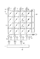
図1は、本発明の第1の実施形態に係わる非冷却型の熱型赤外線センサを示す概略構成図である。この実施形態は、電流読み出し方式であり、4行4列の16画素からなる構成のうち一列が光学的無感度画素となった場合を示している。なお、図では4×4の画素配列を示しているが、実際にはより多数の画素が配列されている。
(First embodiment)
FIG. 1 is a schematic configuration diagram showing an uncooled thermal infrared sensor according to the first embodiment of the present invention. This embodiment is a current readout method, and shows a case where one column is an optically insensitive pixel among the configuration of 16 pixels in 4 rows and 4 columns. Although a 4 × 4 pixel array is shown in the figure, a larger number of pixels are actually arrayed.
図示しない半導体基板上の撮像領域に、赤外線を検出する赤外線検出画素1がマトリクス配置されている。撮像領域には、行方向に複数本の行選択線2が配置され、列方向に複数本の信号線3が配置されている。赤外線検出画素1はpn接合を熱電変換に用いたものであり、各画素は行選択線と信号線との間の交差部に対応する位置に配置されている。また、撮像領域の外には、1本の基準電圧供給線5が行方向に沿って配置されている。
行選択線2は行選択回路20により駆動され、各行毎に順次行選択パルスが印加される。信号線3の一端は信号読み出し回路としての電流電圧変換器30に接続され、各列毎の検出信号が電圧信号として読み出されるようになっている。電流電圧変換器30で読み出された電圧信号は出力回路40に一時記憶され、順次出力されるようになっている。
The
電流電圧変換器30は、非反転入力端に基準電圧供給線5が接続され、反転入力端に信号線3が接続されたオペアンプ31と、このオペアンプ31の出力端と反転入力端との間に挿入された帰還抵抗32から構成されている。そして、オペアンプ31により、基準電圧供給線5の電位が信号線3に与えられるものとなっている。基準電圧供給線5は行選択線2と同一材料、同一構造からなり、行選択回路20の近傍から直流電圧或いは行選択パルスの論理和パルスが印加されている。但し、上記の直流電圧、或いは行選択パルスの論理和パルスの電圧は、行選択パルス電圧よりも低く設定されている。
The current-
出力回路40には、少なくとも一水平期間信号を保持する保持機能と、保持した信号を順次出力する出力機能が含まれている。また、信号線3に発生する信号は極めて微弱であるので、出力回路40の内部には増幅回路を設けることが一般的である。
The
ここまでの構成は従来装置と同様であり、本実施形態ではこれに加えて、基準電圧信号線5に対し、各列毎に基準電圧設定用の定電流源6をそれぞれ接続している。これらの定電流源6は、例えばゲート制御のMOSトランジスタを用いて形成され、画素部の同じ列のpn接合に流れるバイアス電流と同じ電流を流すように制御される。ここで、赤外線検出画素の各pn接合にそれぞれ流すバイアス電流は基本的には共通であるので、定電流源6は画素のpn接合に流すべき共通のバイアス電流と同等の電流を流すように制御されると見なすことができる。
The configuration up to this point is the same as that of the conventional device. In this embodiment, in addition to this, a constant
図2は、図1に示した熱型赤外線センサにおける赤外線検出画素1の構造を示すもので、図2(a)は平面図、図2(b)は図2(a)のA−A’線に沿う断面図である。
2 shows the structure of the
熱電変換のためのpn接合領域115を含む熱電変換部101は単結晶シリコン基板106内部に形成された中空構造107の上に、赤外線吸収部118、120と、熱電変換のために形成されたSOI層108内部のpn接合領域115、これらを接続する配線117、このSOI層108を支持している埋め込みシリコン酸化膜層114とから成る。図では説明上、pn接合が1個の場合のダイオード構造を示す。さらに、画素1を中空構造である中空底部107、中空側部119を介して支持すると共に熱電変換部101からの電気信号を出力するための支持部111と、この画素1と列信号線5および行選択線4とを接続する接続部(図示しない)からなっている。熱電変換部101及び支持部111が中空構造107上に設けられることにより、画素の熱放散が緩慢となり入射赤外線による画素1内部での温度の変調を効率良く行う構造になっている。
The
このような構造を実現するための製造方法については、本発明者等の発明に係わる先特許出願、例えば特開2002−107224号公報,特開2001−281065号公報等に詳細に説明されている。また、光学的無感度画素1Bの構造は、図2に示した画素1の構造と基本的には同一であり、光入射側(図2(b)の上側)に遮光膜としてアルミニウム等の金属薄膜層を形成することで光学的な感度を失わせている。
A manufacturing method for realizing such a structure is described in detail in prior patent applications relating to the inventors' invention, such as JP-A-2002-107224 and JP-A-2001-281055. . Further, the structure of the optical
このように構成された本装置においては、行選択回路20から行選択線2−1、2−2,2−3、そして2−4という順番で行選択パルスが印加される。この行選択パルスが印加された行に配置された赤外線検出画素1の内部のpn接合は順バイアスされ、画素の温度情報を含んだ順バイアス電流が全ての信号線3に流れる。そして、各列毎の電流はオペアンプ31及び帰還抵抗32から成る電流電圧変換器により電圧信号に変換され、出力回路40の内部に一時記憶され、順次出力される。そして、一行分の信号出力が完了したら次の行選択を行い、同様に順次出力するという動作を繰り返すことで二次元イメージを得ることになる。
In this apparatus configured as described above, row selection pulses are applied from the
ここで、行の選択により信号線3に流れる電流は1本の行選択線2から供給されるので、選択された行選択線2の内部にはバイアス電流による電圧降下が発生し、行選択線2には行方向に電位分布が現れてしまう。従来装置のように定電流源6が接続されていないと仮定すると、各列毎の電流電圧変換器の基準入力端の電圧は全て等しくなり、信号線3の電位は基準入力端の電位と等しくなるため、全ての信号線3の電位は等しいものとなる。一方、行選択線2は行方向に電位分布を有しており、従って行方向に対して各画素1に加わる電圧が異なることになる。
Here, since a current flowing through the signal line 3 by selection of a row is supplied from one
つまり、図1に示した電流読み出し方式においては、選択された行選択線2に接続されたpn接合が全て順バイアスとなり、全ての列の信号線3からバイアス電流が流れることになるが、この電流は一つの行選択線2から供給されているので、選択された行選択線2の内部にはバイアス電流による電圧降下が発生し、行選択線2には列方向に電位分布が現れてしまう。
That is, in the current reading method shown in FIG. 1, all the pn junctions connected to the selected
行選択線内部の電圧降下の様子を、図3に示す。図3は、行選択線2の抵抗値を一列当たり0.55Ωと仮定して、行選択線2を片側から3Vで駆動する構造での、横軸が列、縦軸が行選択線電位である。パラメータとして、バイアス電流を1μAから20μAとし、列に関しては320列のデバイスを想定している。
FIG. 3 shows the voltage drop inside the row selection line. In FIG. 3, assuming that the resistance of the
図3に示すように、バイアス電流が1μAにおいても30mV程度の電圧降下が発生し、バイアス電流が10μAでは280mV,20μAでは570mVもの電圧降下が発生してしまう。 As shown in FIG. 3, a voltage drop of about 30 mV occurs even when the bias current is 1 μA, and a voltage drop of 280 mV occurs when the bias current is 10 μA and 570 mV when the bias current is 20 μA.
このような電圧分布が発生した場合には、電流読み出し方式においては、一定電圧のバイアスを行うという動作の前提が崩れてしまい、順バイアスのバイアス電流は大きく変動し、正常な動作ができなくなってしまう。また、後述する電圧読み出し方式においては列方向で信号出力が傾きを持つ、いわゆるシェーディングが発生し、或いは出力回路40の内部で飽和してしまい出力が得られなくなることもある。
If such a voltage distribution occurs, the current read method loses the premise of the operation of biasing at a constant voltage, the forward bias bias current fluctuates greatly, and normal operation cannot be performed. End up. In the voltage reading method described later, so-called shading in which the signal output has a gradient in the column direction may occur, or the output may be saturated inside the
そこで本実施形態では、基準電圧供給線5に対し、各列において基準電圧設定用の定電流源6を接続し、画素部のpn接合に流れるバイアス電流と同じ電流を流すよう制御している。このような設定により、基準電圧供給線5の電位分布を行選択線2と同じ電圧分布とすることが可能になる。
Therefore, in the present embodiment, a constant
その結果、各列の信号線3の電位は、行選択線2と同一の電位分布を持つ基準電圧供給線5の電位と等しくなる。従って、行選択線2と基準電圧供給線5の各々の電位分布は相殺され、各々の列の選択画素には一定のバイアス電圧を印加することが可能となる。
As a result, the potential of the signal line 3 in each column becomes equal to the potential of the reference
このバイアス電圧は、行選択パルスの電圧と、上記の基準電圧供給線5をドライブする電圧との差によって決定できるので、所望の動作電圧を与えることが可能である。例えば、行選択パルス電圧を3Vとして、画素pn接合に0.8Vのバイアス電圧を印加したい場合には、基準電圧供給線5のドライブパルスとして3−0.8=2.2[V]の電圧を与えればよいことになる。
Since this bias voltage can be determined by the difference between the voltage of the row selection pulse and the voltage for driving the reference
このとき、バイアス電流が10μAとすれば、行選択回路20から最も離れた列が320列目だとした場合、行選択線2の電位は2.72Vに低下してしまうが、同時に基準電圧供給線5の電位も1.92Vに低下しているので、画素のpn接合の順バイアス電圧は所望の0.8Vのままである。なお、信号線3を流れるバイアス電流は、各列において並列に流れているのでその電圧降下は十分に低く無視できる。
At this time, if the bias current is 10 μA, if the column farthest from the
また、厳密には各画素を流れる電流には各画素の温度情報が含まれているので同一のバイアス電圧を印加したとしても同一の電流が流れるわけでなく、当然信号成分の電流変動が発生している。しかし、画素部の温度上昇は被写体温度変化が1[K]に対して5[mK]程度と極めて微弱であり、自己加熱と比較して十分に無視ができるレベルであるので、各列に配置した定電流源6の電流を画素部のpn接合を流れる順バイアス電流に設定することは実際上難しくはない。
Strictly speaking, since the current flowing through each pixel includes the temperature information of each pixel, even if the same bias voltage is applied, the same current does not flow, and naturally the current fluctuation of the signal component occurs. ing. However, the temperature rise of the pixel portion is extremely weak, with the subject temperature change being about 5 [mK] with respect to 1 [K], and is a level that can be sufficiently ignored as compared with the self-heating. In practice, it is not difficult to set the current of the constant
なお、図1の構成において、各列からの出力電圧は、電流電圧変換によって得られた信号電圧に、基準電圧供給線5の電位分布が加算されたものとなる。このため、出力画像が列方向に輝度の傾きを持ってしまう、いわゆるシェーディングが発生してしまう場合がある。このシェーディングが問題となる場合は、外部回路によりシェーディング補正を行うようにすればよい。
In the configuration of FIG. 1, the output voltage from each column is obtained by adding the potential distribution of the reference
このように本実施形態によれば、電流読み出し方式の熱型赤外線センサにおいて、基準電圧供給線5に対して、各列毎に対応する位置に定電流源6をそれぞれ接続することにより、バイアス電流が行選択線2を流れることにより発生する電圧降下、及びその結果である行選択線内部の列方向電位分布と同等の電位分布を与えるようにしているので、各列毎に信号線3と行選択線2との間の電圧を一定とすることが可能となる。従って、電流読み出し方式本来の高感度特性を得ることができる。
As described above, according to the present embodiment, in the current readout type thermal infrared sensor, the bias current is obtained by connecting the constant
(第2の実施形態)
図4は、本発明の第2の実施形態に係わる非冷却型の熱型赤外線センサを示す概略構成図である。なお、図1と同一部分には同一符号を付して、その詳しい説明は省略する。
(Second Embodiment)
FIG. 4 is a schematic configuration diagram showing an uncooled thermal infrared sensor according to the second embodiment of the present invention. The same parts as those in FIG. 1 are denoted by the same reference numerals, and detailed description thereof is omitted.
本実施形態は、電流読み出し方式におけるシェーディング補正のための構成である。図1に示した定電圧バイアス化した電流読み出し回路にシェーディング補正回路として、オペアンプ31からの信号電圧から基準電圧供給線5の電圧を減算するための差動増幅回路50を付加したものである。差動増幅回路50については、オペアンプと抵抗とを組み合わせることで容易に実現可能であり、ここではその詳細については説明を省略する。
The present embodiment is a configuration for shading correction in the current readout method. A
このように本実施形態によれば、行選択線2の各列における電流に依存するオペアンプ31の信号出力から、基準電圧供給線5に現れている電圧を減算処理することで、電流読み出し方式において発生するシェーディングを除去することができる。しかも、このシェーディング補正をオンチップでアナログ領域において行うことが可能となるため、シェーディング補正のための外部回路等も不要となる。
As described above, according to the present embodiment, the voltage appearing on the reference
(第3の実施形態)
図5は、本発明の第3の実施形態に係わる非冷却型の熱型赤外線センサを示す概略構成図である。なお、図1及び図2と同一部分には同一符号を付して、その詳しい説明は省略する。
(Third embodiment)
FIG. 5 is a schematic configuration diagram showing an uncooled thermal infrared sensor according to the third embodiment of the present invention. 1 and 2 are denoted by the same reference numerals, and detailed description thereof is omitted.
本実施形態では、シェーディング補正を行う電流読み出し回路を備えた図4の構成に差動増幅器60を付加した構成になっている。即ち、有効感度画素列に対応して差動増幅器60がそれぞれ設けられ、各列の差動増幅器60の−入力端には有効感度画素列の差動増幅器50の出力端が接続され、+入力端には無感度画素列の差動増幅器50の出力端が接続されている。
In the present embodiment, a
本実施形態においては、行選択線2の内部の電圧降下の影響は、各列に配置された定電流回路6と基準電圧供給線5により排除され、さらに基準電圧供給線5の電位分布に起因するシェーディングも差動増幅回路50により除去される。これに加えて、無感度画素1Bからなる無感度画素列からの信号を除去するための差動増幅器60を設けることにより、無感度画素列から得られるバイアス電流成分及び自己加熱電流成分を除去することが可能となる。
In the present embodiment, the influence of the voltage drop inside the
バイアス電流が10μA程度の場合、被写体温度差が1[K]の場合、信号電流は3nA程度と非常に微弱である。従って、バイアス電流成分を減算処理することにより真の信号出力のみを抽出することは後段での信号処理を容易にすることができる。その結果、行選択線2の電圧降下に起因する問題は解決され、さらに雑音成分であるバイアス電流成分、自己加熱電流成分も除去された、真の信号出力のみを出力回路40から出力することが可能となる。
When the bias current is about 10 μA and the subject temperature difference is 1 [K], the signal current is very weak, about 3 nA. Therefore, extracting only the true signal output by subtracting the bias current component can facilitate signal processing at a later stage. As a result, the problem caused by the voltage drop of the
(第4の実施形態)
図6は、本発明の第4の実施形態に係わる非冷却型の熱型赤外線センサを示す概略構成図である。この実施形態は、電圧読み出し方式であり、4行4列の16画素からなる構成のうち一列が光学的無感度画素となった場合を示している。なお、図では4×4の画素配列を示しているが、実際にはより多数の画素が配列されている。なお、図1と同一部分には同一符号を付して、その詳しい説明は省略する。
(Fourth embodiment)
FIG. 6 is a schematic configuration diagram showing an uncooled thermal infrared sensor according to the fourth embodiment of the present invention. This embodiment is a voltage readout method, and shows a case where one column of the configuration of 16 pixels in 4 rows and 4 columns is an optically insensitive pixel. Although a 4 × 4 pixel array is shown in the figure, a larger number of pixels are actually arrayed. The same parts as those in FIG. 1 are denoted by the same reference numerals, and detailed description thereof is omitted.
赤外線検出画素1,行選択線2,信号線3,基準電圧供給線5,基準電圧設定用定電流源6,行選択回路20,及び出力回路40は、図1の構成と同じである。信号線3の一端側には、電圧読み出し用の定電流源4が接続されている。信号線3の他端側には、電流電圧変換器ではなく、差動増幅器70から成る読み出し回路が接続されている。即ち、列毎に差動増幅器70が設けられ、差動増幅器70の一方の入力端には信号線3が接続され、他方の入力端には基準電圧供給線5が接続されている。
The
行選択動作については、基本的に図1に示した電流読み出し方式と同じであり、行選択回路40から行選択線2−1,2−1,2−3,2−4という順番で行選択パルスが印加される。この行選択パルスが印加された行に配置された赤外線検出画素1の内部のpn接合は順バイアスされ、行選択動作がなされる。定電流源4により供給される定電流は、信号線3,画素1,行選択線2,行選択回路20の電流パスを流れ、画素1の内部のpn接合の温度情報に応じて電圧情報が各列の信号線3に発生する。
The row selection operation is basically the same as that of the current reading method shown in FIG. 1, and row selection is performed in the order of row selection lines 2-1, 2-1, 2-3, 2-4 from the
信号線に発生した電圧情報は、差動増幅器により基準電圧供給線の電圧と減算され、この減算出力が出力回路に一時記憶され、順次出力される。そして、一行分の信号出力が完了したら、次の行選択を行い、同様に順次出力するという動作を繰り返すことで二次元イメージを得ることになる。 The voltage information generated in the signal line is subtracted from the voltage of the reference voltage supply line by the differential amplifier, and this subtracted output is temporarily stored in the output circuit and sequentially output. When the signal output for one row is completed, the next row is selected and the operation of sequentially outputting the same is repeated to obtain a two-dimensional image.
本実施形態では、従来構造の電圧読み出し方式である構成に、各列に配置された定電流源6と、行選択線2と同一材料、同一構造で形成された基準電圧供給線5及びその駆動部が付加され、更に信号線3からの信号電圧から基準電圧供給線5の電圧を減算するための差動増幅回路70が付加されている。差動増幅回路70については、オペアンプと抵抗とを組み合わせることで容易に実現可能であり、ここではその詳細については説明を省略する。
In the present embodiment, the configuration of the conventional voltage readout method is such that the constant
本実施形態においては、基準電圧供給線5に対し列毎に定電流源6を接続することにより、基準電圧供給線5の電圧降下分布は行選択線2の電圧降下分布と等しくなるように設定が可能である。従って、行選択線2の各列における電位に依存する各列信号線3からの信号出力から、基準電圧供給線5に現れている電圧を減算処理することで、電圧読み出し方式において発生するシェーディングをオンチップでアナログ領域において除去することが可能となる。
In the present embodiment, the voltage drop distribution of the reference
(第5の実施形態)
図7は、本発明の第5の実施形態に係わる非冷却型の熱型赤外線センサを示す概略構成図である。なお、図6と同一部分には同一符号を付して、その詳しい説明は省略する。
(Fifth embodiment)
FIG. 7 is a schematic configuration diagram showing an uncooled thermal infrared sensor according to the fifth embodiment of the present invention. The same parts as those in FIG. 6 are denoted by the same reference numerals, and detailed description thereof is omitted.
この実施形態は、電圧読み出し方式の図6の構成に差動増幅器80を付加した構成になっている。即ち、有効感度画素列に対応して差動増幅器80がそれぞれ設けられ、各列の差動増幅器80の+入力端には有効感度画素列の差動増幅器70の出力端が接続され、−入力端には無感度画素列の差動増幅器70の出力端が接続されている。
In this embodiment, a
本実施形態においては、行選択線2内部の電圧降下の影響は、各列に配置された定電流回路6と基準電圧供給線5により排除され、さらに行選択線2の電位分布に起因するシェーディングは差動増幅回路70により除去される。これに加えて、無感度画素1Bからなる無感度画素列からの信号を除去するための差動増幅器80を設けることにより、無感度画素列から得られるバイアス電流成分、及び自己加熱電流成分を除去することが可能となる。従って、第3の実施形態と同様の効果が得られる。
In the present embodiment, the influence of the voltage drop inside the
(第6の実施形態)
図8は、本発明の第6の実施形態に係わる非冷却型の熱型赤外線センサを示す概略構成図である。なお、図5と同一部分には同一符号を付して、その詳しい説明は省略する。
(Sixth embodiment)
FIG. 8 is a schematic configuration diagram showing an uncooled thermal infrared sensor according to the sixth embodiment of the present invention. In addition, the same code | symbol is attached | subjected to FIG. 5 and an identical part, and the detailed description is abbreviate | omitted.
前述した第1〜第5の実施形態により、行選択線の電圧降下に起因するバイアス不良やシェーディング発生などを防止することができる。一方で、読み出し回路にオペアンプを用いることによる消費電力の増大が発生する。特に、前記図5のように各列にオペアンプ回路を3個有する電流読み出し回路の場合には、電源電圧として±3Vを供給するCMOSオペアンプ回路を用い、オペアンプのバイアス電流を100μAまで絞った状態でも、QVGA(320×240画素)程度の画素規模では、320列の読み出し回路が常時動作することを考えると、読み出し回路だけの消費電力が600mWにもなってしまう。そして、画素規模が大規模化することでその影響はさらに加速する。 According to the first to fifth embodiments described above, it is possible to prevent a bias failure or a shading caused by a voltage drop of the row selection line. On the other hand, power consumption increases due to the use of an operational amplifier in the readout circuit. In particular, in the case of a current readout circuit having three operational amplifier circuits in each column as shown in FIG. 5, a CMOS operational amplifier circuit that supplies ± 3 V as a power supply voltage is used, and the bias current of the operational amplifier is reduced to 100 μA. In a pixel scale of about QVGA (320 × 240 pixels), considering that the readout circuit of 320 columns always operates, the power consumption of the readout circuit alone becomes 600 mW. And the influence is further accelerated by increasing the pixel scale.
そこで本実施形態は、図8に示すように、先の第3の実施形態(図5)の構成に加え、基準パルス発生器301からの基準パルスを受けてVd駆動パルスを発生する駆動パルス発生器302を設けている。基準パルス発生器301は、行選択回路20に基準パルスを与え、行選択線2を順番に駆動するためのものであり、第1〜第5の実施形態においても設けられている。駆動パルス発生器302は、基準パルスを基に駆動パルスVBを発生するものであり、この駆動パルスVBが信号読み出し回路(30,50,60)を構成する各オペアンプ(31,51,61)に供給されている。
Therefore, in the present embodiment, as shown in FIG. 8, in addition to the configuration of the third embodiment (FIG. 5), the drive pulse generation for generating the Vd drive pulse in response to the reference pulse from the
行選択回路20の構成としては、シフトレジスタ回路と基準パルス発生器301の両出力の論理積を出力する回路構成を用いることが可能である。基準パルス発生器301及び駆動パルス発生器302は、赤外線センサチップ外部に設けることも、チップ上に形成することも可能である。
As a configuration of the
オペアンプ31,51,61は、いずれもCMOSオペアンプであり、その回路構成は図9に示すようなものであり、外部からのVB入力によりバイアス電流を制御する構成となっている。即ち、差動増幅回路を構成するMOSトランジスタQ1〜Q4と、その出力を受けるバッファ回路を構成するMOSトランジスタQ5と、スイッチング素子として機能するMOSトランジスタQ6,Q7で構成されている。
The
オペアンプのバイアス入力端VBがVbであれば、Q6,Q7はオンし、このオペアンプは動作する。バイアス入力端VBが−Vddであれば、Q6,Q7はオフするため、このオペアンプは動作しない、即ち電流が流れない。なお、図8においては、図9に示したCMOSオペアンプ回路を図10のように表記した回路として表現している。 If the bias input terminal VB of the operational amplifier is Vb, Q6 and Q7 are turned on, and this operational amplifier operates. If the bias input terminal VB is −Vdd, Q6 and Q7 are turned off, so that this operational amplifier does not operate, that is, no current flows. In FIG. 8, the CMOS operational amplifier circuit shown in FIG. 9 is expressed as a circuit expressed as shown in FIG.
図8に示されるように、オペアンプ31,51,61のバイアス入力端VBは共通になっており、基準パルス発生器301からのパルスによりVbと−Vddのパルスを生成する駆動パルス発生器302からVB線303にパルス電圧が印加され、行選択パルスと同期してオペアンプ31,51,61は間欠駆動されることになる。
As shown in FIG. 8, the bias input terminals VB of the
このように本実施形態によれば、カラム読み出し回路を構成するオペアンプ31,51,61は、読み出し動作を行う期間だけ動作することになり、その消費電力を大幅に低減することが可能となる。例えば、画素規模としてQVGA(320列×240行)の素子を60フレーム/秒のフレームレートで駆動する場合を考える。
As described above, according to the present embodiment, the
マスタークロックとして32.76MHzのクロックを用いるとすれば、基準パルス幅:Δtは30.5ns、1フレーム期間は546000Δt=16.7msとなる。1水平期間×(240行+α)により1フレームが構成されるので、1水平期間を2000Δt=60μsとする。 If a clock of 32.76 MHz is used as the master clock, the reference pulse width: Δt is 30.5 ns, and one frame period is 546000 Δt = 16.7 ms. Since one frame is composed of one horizontal period × (240 rows + α), one horizontal period is set to 2000 Δt = 60 μs.
1水平期間中の信号読み出しパルス幅を2Δtとして、一列の読み出しにかかる時間は4Δtとなる。320列+αの読み出しを行うので、α=40として読み出し期間は1440Δtとなる。従って、水平ブランキング期間は560Δt=17μs。この期間にリセット動作と行選択動作を行うので、各々5μsと10μsになる。 Assuming that the signal readout pulse width during one horizontal period is 2Δt, the time required to read out one row is 4Δt. Since 320 columns + α are read out, α = 40 and the reading period is 1440Δt. Therefore, the horizontal blanking period is 560 Δt = 17 μs. Since the reset operation and the row selection operation are performed during this period, they become 5 μs and 10 μs, respectively.
オペアンプ回路を上記の行選択期間のみ動作させることにすれば、1水平期間:60μsのうち、行選択期間:10μsのみの間欠動作になり、オペアンプの消費電力は1/6に低減される。 If the operational amplifier circuit is operated only in the above-described row selection period, the intermittent operation is performed only in the row selection period: 10 μs in one horizontal period: 60 μs, and the power consumption of the operational amplifier is reduced to 1/6.
従って、図10に示したCMOSオペアンプの合計バイアス電流を100μA、電源電圧を±3Vとした場合、QVGA規模のデバイスではオペアンプ部分のみの消費電力は600mWから100mWに大幅に低減されることになる。 Therefore, when the total bias current of the CMOS operational amplifier shown in FIG. 10 is 100 μA and the power supply voltage is ± 3 V, the power consumption of only the operational amplifier portion is greatly reduced from 600 mW to 100 mW in a QVGA scale device.
このように本実施形態によれば、先の第3の実施形態の構成に加え、信号読み出し回路(30,50,60)を行選択線2の駆動に同期して駆動する駆動パルス発生器302を設けたことにより、先の第1の実施形態と同様の効果が得られるのは勿論のこと、信号読み出し回路を構成するオペアンプの消費電力を大幅に低減することができる。
As described above, according to the present embodiment, in addition to the configuration of the third embodiment, the
また、以上の説明においては、信号読み出し回路を構成する電流電圧変換器、差動増幅器としてオペアンプを用いた回路として説明してきたが、それ以外の回路構成によっても同様な効果を得ることが可能である。また、図8の構成以外による電流読み出し、及び電圧読み出しデバイスにおいて、本実施形態の考えを適用することによっても同様の効果を得ることができる。即ち、第3の実施形態以外に、第1,第2及び第4,第5の実施形態にも、信号読み出し回路の選択駆動を行う考えを同様に適用することが可能である。 In the above description, the current / voltage converter constituting the signal readout circuit and the circuit using the operational amplifier as the differential amplifier have been described. However, the same effect can be obtained with other circuit configurations. is there. Further, the same effect can be obtained by applying the idea of the present embodiment to a current reading and voltage reading device other than the configuration of FIG. That is, in addition to the third embodiment, the idea of performing selective driving of the signal readout circuit can be similarly applied to the first, second, fourth, and fifth embodiments.
(変形例)
なお、本発明は上述した各実施形態に限定されるものではない。読み出し回路としての電流電圧変換器や差動増幅器の構成は、オペアンプや抵抗に限るものではなく、仕様に応じて適宜変更可能である。また、赤外線検出画素は図2に示す構成に限るものではなく、赤外線吸収構造と熱電変換手段を有するものであればよい。さらに、無感度画素列は必ずしも1列に限るものではなく、複数列にしてもよい。無感度画素列を複数にした場合、無感度画素列における信号の平均値を参照信号として用いればよい。
(Modification)
The present invention is not limited to the above-described embodiments. The configurations of the current-voltage converter and the differential amplifier as the readout circuit are not limited to the operational amplifier and the resistor, and can be appropriately changed according to the specification. In addition, the infrared detection pixel is not limited to the configuration shown in FIG. 2 and may be any pixel having an infrared absorption structure and thermoelectric conversion means. Further, the insensitive pixel column is not necessarily limited to one column, and may be a plurality of columns. When there are a plurality of insensitive pixel columns, an average value of signals in the insensitive pixel column may be used as a reference signal.
その他、本発明の要旨を逸脱しない範囲で、種々変形して実施することができる。 In addition, various modifications can be made without departing from the scope of the present invention.
1…赤外線検出画素
2…行選択線
3…信号線
4…電圧読み出し用定電流源
5…基準電圧供給線
6…基準電圧設定用定電流源
10…撮像領域
20…行選択回路
30…電流電圧変換器(信号読み出し回路)
31…オペアンプ
32…抵抗
40…出力回路
50,60,70,80…差動増幅器
301…基準パルス発生器
302…駆動パルス発生器
303…VB線
DESCRIPTION OF
DESCRIPTION OF
Claims (9)
この撮像領域内に行方向に配置された複数の行選択線と、
前記撮像領域内に列方向に配置された複数の信号線と、
これらの信号線に発生した電気信号を読み出すために各列にそれぞれ配置された信号読み出し回路と、
前記複数の行選択線を駆動するための行選択回路と、
前記撮像領域外に前記行選択線と平行に配置された基準電圧供給線と、
前記基準電圧供給線に直流電圧又はパルス電圧を直接印加する手段と、
前記信号線に対して各列毎に異なる基準電圧を与えるために、前記基準電圧供給線に対し各列に対応する位置にそれぞれ接続され、同じ列の赤外線検出画素のpn接合に流れるバイアス電流と同等の電流を流す基準電圧設定用定電流源と、
前記信号読み出し回路からの出力信号を出力するための出力回路と、
を具備してなることを特徴とする赤外線センサ。 An imaging region in which infrared detection pixels for detecting incident infrared rays are two-dimensionally arranged on a semiconductor substrate;
A plurality of row selection lines arranged in the row direction in the imaging region;
A plurality of signal lines arranged in a column direction in the imaging region;
A signal readout circuit arranged in each column for reading out electrical signals generated in these signal lines;
A row selection circuit for driving the plurality of row selection lines;
A reference voltage supply line arranged in parallel to the row selection line outside the imaging region;
Means for directly applying a DC voltage or a pulse voltage to the reference voltage supply line;
In order to give a different reference voltage for each column to the signal line, a bias current that is connected to the reference voltage supply line at a position corresponding to each column and flows to the pn junction of the infrared detection pixel in the same column, A constant current source for setting a reference voltage for flowing an equivalent current;
An output circuit for outputting an output signal from the signal readout circuit;
An infrared sensor comprising:
この撮像領域内に行方向に配置された複数の行選択線と、
これらの行選択線を順次駆動するための行選択回路と、
前記撮像領域内に列方向に配置された複数の信号線と、
これらの信号線に発生した電気信号を読み出すために各列にそれぞれ配置された複数の信号読み出し回路と、
これらの信号読み出し回路を前記行選択線の駆動に同期して駆動する駆動回路と、
前記撮像領域外に前記行選択線と平行に配置された基準電圧供給線と、
前記信号線に対して各列毎に異なる基準電圧を与えるために、前記基準電圧供給線に対し各列に対応する位置にそれぞれ接続され、同じ列の赤外線検出画素のpn接合に流れるバイアス電流と同等の電流を流す基準電圧設定用定電流源と、
前記信号読み出し回路からの出力信号を出力するための出力回路と、
を具備してなることを特徴とする赤外線センサ。 An imaging region in which infrared detection pixels for detecting incident infrared rays are two-dimensionally arranged on a semiconductor substrate;
A plurality of row selection lines arranged in the row direction in the imaging region;
A row selection circuit for sequentially driving these row selection lines;
A plurality of signal lines arranged in a column direction in the imaging region;
A plurality of signal readout circuits arranged in each column to read out electrical signals generated in these signal lines;
A driving circuit for driving these signal readout circuits in synchronization with the driving of the row selection lines;
A reference voltage supply line arranged in parallel to the row selection line outside the imaging region;
In order to give a different reference voltage for each column to the signal line, a bias current that is connected to the reference voltage supply line at a position corresponding to each column and flows to the pn junction of the infrared detection pixel in the same column, A constant current source for setting a reference voltage for flowing an equivalent current;
An output circuit for outputting an output signal from the signal readout circuit;
An infrared sensor comprising:
前記信号読み出し回路は、前記無感度画素列以外の有効感度画素列における前記電流電圧変換器の各出力電圧と、前記無感度画素列における前記電流電圧変換器の出力電圧との差分をそれぞれ増幅して出力する差動増幅器を更に備えていることを特徴とする請求項3記載の赤外線センサ。 One or more columns of pixels in the imaging region are optical insensitive pixels that do not detect incident infrared radiation,
The signal readout circuit amplifies a difference between each output voltage of the current-voltage converter in an effective sensitivity pixel column other than the insensitive pixel column and an output voltage of the current-voltage converter in the insensitive pixel column. The infrared sensor according to claim 3, further comprising a differential amplifier for outputting the output.
前記信号読み出し回路は、前記無感度画素列以外の有効感度画素列における第1の差動増幅器の各出力電圧と、前記無感度画素列における第1の差動増幅器の出力電圧との差分をそれぞれ増幅して出力する第2の差動増幅器を更に備えていることを特徴とする請求項4又は6記載の赤外線センサ。 One or more columns of pixels in the imaging region are optical insensitive pixels that do not detect incident infrared radiation,
The signal readout circuit calculates a difference between each output voltage of the first differential amplifier in the effective sensitivity pixel column other than the insensitive pixel column and an output voltage of the first differential amplifier in the insensitive pixel column, respectively. 7. The infrared sensor according to claim 4, further comprising a second differential amplifier that amplifies and outputs.
該オペアンプは、外部入力電圧によりそのバイアス電流を制御することが可能な構成をとっており、
前記駆動回路は、前記外部入力電圧としてパルス状の電圧を前記オペアンプに与えることで前記信号読み出し回路をオンオフすること、
を特徴とする請求項2記載の赤外線センサ。 The signal readout circuit includes an operational amplifier having a signal input terminal connected to the signal line and a reference input terminal connected to the reference voltage supply line for each column to which the circuit corresponds.
The operational amplifier has a configuration capable of controlling the bias current by an external input voltage,
The drive circuit turns on and off the signal readout circuit by applying a pulse voltage as the external input voltage to the operational amplifier.
The infrared sensor according to claim 2.
Priority Applications (1)
| Application Number | Priority Date | Filing Date | Title |
|---|---|---|---|
| JP2003362199A JP4153861B2 (en) | 2003-05-14 | 2003-10-22 | Infrared sensor |
Applications Claiming Priority (2)
| Application Number | Priority Date | Filing Date | Title |
|---|---|---|---|
| JP2003136012 | 2003-05-14 | ||
| JP2003362199A JP4153861B2 (en) | 2003-05-14 | 2003-10-22 | Infrared sensor |
Publications (2)
| Publication Number | Publication Date |
|---|---|
| JP2004364241A JP2004364241A (en) | 2004-12-24 |
| JP4153861B2 true JP4153861B2 (en) | 2008-09-24 |
Family
ID=34067228
Family Applications (1)
| Application Number | Title | Priority Date | Filing Date |
|---|---|---|---|
| JP2003362199A Expired - Fee Related JP4153861B2 (en) | 2003-05-14 | 2003-10-22 | Infrared sensor |
Country Status (1)
| Country | Link |
|---|---|
| JP (1) | JP4153861B2 (en) |
Families Citing this family (8)
| Publication number | Priority date | Publication date | Assignee | Title |
|---|---|---|---|---|
| JP2008022315A (en) * | 2006-07-13 | 2008-01-31 | Mitsubishi Electric Corp | Thermal infrared detection circuit |
| US8357900B2 (en) | 2008-01-08 | 2013-01-22 | Mitsubishi Electric Corporation | Thermal infrared detecting device |
| JP4685949B2 (en) * | 2009-03-17 | 2011-05-18 | 三菱電機株式会社 | Infrared solid-state image sensor |
| JP5335006B2 (en) | 2010-02-26 | 2013-11-06 | 三菱電機株式会社 | Infrared solid-state image sensor |
| JP5425127B2 (en) | 2011-03-09 | 2014-02-26 | 株式会社東芝 | Solid-state image sensor |
| WO2013145757A1 (en) | 2012-03-29 | 2013-10-03 | 旭化成エレクトロニクス株式会社 | Light receiving device |
| US10848689B2 (en) * | 2016-04-19 | 2020-11-24 | Mitsubishi Electric Corporation | Infrared imaging element detecting temperature change, and infrared camera using the same element |
| US10451487B1 (en) * | 2018-08-23 | 2019-10-22 | Raytheon Company | Per-pixel dark reference bolometer |
-
2003
- 2003-10-22 JP JP2003362199A patent/JP4153861B2/en not_active Expired - Fee Related
Also Published As
| Publication number | Publication date |
|---|---|
| JP2004364241A (en) | 2004-12-24 |
Similar Documents
| Publication | Publication Date | Title |
|---|---|---|
| JP3866069B2 (en) | Infrared solid-state imaging device | |
| JP4372097B2 (en) | Infrared sensor, infrared camera, driving method of infrared sensor, and driving method of infrared camera | |
| US6770881B2 (en) | Infrared sensor | |
| JP5335006B2 (en) | Infrared solid-state image sensor | |
| JP4898522B2 (en) | Imaging apparatus, radiation imaging system, and imaging apparatus control method | |
| JP2005175418A (en) | Photoelectric conversion apparatus | |
| JP2993557B2 (en) | Thermal infrared imaging apparatus and driving method thereof | |
| JPWO2017141727A1 (en) | Solid-state imaging device, driving method of solid-state imaging device, and electronic apparatus | |
| JP3655232B2 (en) | Infrared sensor | |
| JP4343144B2 (en) | Infrared sensor | |
| JP4153861B2 (en) | Infrared sensor | |
| US7737400B2 (en) | Bolometer type uncooled infrared ray sensor and method for driving the same | |
| JP2008022315A (en) | Thermal infrared detection circuit | |
| JP2002300475A (en) | Infrared sensor and method for driving the same | |
| JPH10227689A (en) | Infrared detector and infrared focal plane array | |
| JP4331160B2 (en) | Infrared sensor and driving method thereof | |
| JP3657885B2 (en) | Infrared sensor device and driving method thereof | |
| JP4277619B2 (en) | Solid-state image sensor | |
| JP3648506B2 (en) | Infrared imaging device | |
| JP2004336099A (en) | Thermal type infrared solid-state imaging apparatus | |
| USRE38527E1 (en) | Thermal-type infrared imaging device | |
| US11985442B2 (en) | Bias circuit with improved noise performance | |
| JP3998599B2 (en) | Thermal infrared solid-state imaging device | |
| JP2017163403A (en) | Infrared image pickup element and infrared imaging apparatus |
Legal Events
| Date | Code | Title | Description |
|---|---|---|---|
| A621 | Written request for application examination |
Free format text: JAPANESE INTERMEDIATE CODE: A621 Effective date: 20050209 |
|
| A977 | Report on retrieval |
Free format text: JAPANESE INTERMEDIATE CODE: A971007 Effective date: 20071030 |
|
| A131 | Notification of reasons for refusal |
Free format text: JAPANESE INTERMEDIATE CODE: A131 Effective date: 20071113 |
|
| A521 | Request for written amendment filed |
Free format text: JAPANESE INTERMEDIATE CODE: A523 Effective date: 20080115 |
|
| TRDD | Decision of grant or rejection written | ||
| A01 | Written decision to grant a patent or to grant a registration (utility model) |
Free format text: JAPANESE INTERMEDIATE CODE: A01 Effective date: 20080701 |
|
| A01 | Written decision to grant a patent or to grant a registration (utility model) |
Free format text: JAPANESE INTERMEDIATE CODE: A01 |
|
| A61 | First payment of annual fees (during grant procedure) |
Free format text: JAPANESE INTERMEDIATE CODE: A61 Effective date: 20080704 |
|
| FPAY | Renewal fee payment (event date is renewal date of database) |
Free format text: PAYMENT UNTIL: 20110711 Year of fee payment: 3 |
|
| FPAY | Renewal fee payment (event date is renewal date of database) |
Free format text: PAYMENT UNTIL: 20120711 Year of fee payment: 4 |
|
| FPAY | Renewal fee payment (event date is renewal date of database) |
Free format text: PAYMENT UNTIL: 20130711 Year of fee payment: 5 |
|
| LAPS | Cancellation because of no payment of annual fees |