JP4081350B2 - Method for generating an address configuration for a memory - Google Patents
Method for generating an address configuration for a memory Download PDFInfo
- Publication number
- JP4081350B2 JP4081350B2 JP2002323686A JP2002323686A JP4081350B2 JP 4081350 B2 JP4081350 B2 JP 4081350B2 JP 2002323686 A JP2002323686 A JP 2002323686A JP 2002323686 A JP2002323686 A JP 2002323686A JP 4081350 B2 JP4081350 B2 JP 4081350B2
- Authority
- JP
- Japan
- Prior art keywords
- address
- lines
- memory
- sequence
- column
- Prior art date
- Legal status (The legal status is an assumption and is not a legal conclusion. Google has not performed a legal analysis and makes no representation as to the accuracy of the status listed.)
- Expired - Fee Related
Links
Images


Classifications
-
- G—PHYSICS
- G06—COMPUTING; CALCULATING OR COUNTING
- G06F—ELECTRIC DIGITAL DATA PROCESSING
- G06F12/00—Accessing, addressing or allocating within memory systems or architectures
- G06F12/02—Addressing or allocation; Relocation
-
- G—PHYSICS
- G11—INFORMATION STORAGE
- G11C—STATIC STORES
- G11C8/00—Arrangements for selecting an address in a digital store
- G11C8/10—Decoders
-
- G—PHYSICS
- G11—INFORMATION STORAGE
- G11C—STATIC STORES
- G11C8/00—Arrangements for selecting an address in a digital store
- G11C8/12—Group selection circuits, e.g. for memory block selection, chip selection, array selection
Landscapes
- Engineering & Computer Science (AREA)
- Microelectronics & Electronic Packaging (AREA)
- Theoretical Computer Science (AREA)
- Physics & Mathematics (AREA)
- General Engineering & Computer Science (AREA)
- General Physics & Mathematics (AREA)
- For Increasing The Reliability Of Semiconductor Memories (AREA)
- Read Only Memory (AREA)
- Static Random-Access Memory (AREA)
- Techniques For Improving Reliability Of Storages (AREA)
Description
【0001】
【発明の属する技術分野】
本発明は、情報記憶装置に関する。より詳細には、本発明は、半導体メモリのためのアドレスロジックに関する。
【0002】
【従来の技術】
PDA、ハンドヘルドコンピュータ、デジタルカメラおよびデジタルミュージックプレイヤ等の携帯機器は、データ、デジタルイメージおよびMP3ファイルを格納するためのメモリを有する。これら携帯機器に対して異なるタイプのメモリが入手可能である。従来のメモリタイプには、フラッシュメモリ、小型ハードドライブ、小型コンパクトディスクおよび磁気テープが含まれる。しかしながら、これらメモリタイプの各々には、以下の限界のうちの1つまたは複数がある。すなわち、物理サイズが大きいこと、記憶容量が低いこと、コストが相対的に高いこと、頑強性に乏しいこと、アクセス時間が低速であること、消費電力が高いこと、である。
【0003】
半導体ダイオードベースのOTPメモリが、2001年6月5日に出願された本願と同一の譲受人に譲渡された米国特許出願第09/875,356号に開示されている。従来のメモリと比較して、ダイオードベースのメモリは、耐衝撃性が高く、消費電力が低く、アクセス時間が高速であり、転送速度が適度であり、記憶容量が十分である。ダイオードベースのメモリは、携帯機器の標準携帯インタフェース(例えば、PCMCIA、CF)に適合することができる。
【0004】
複数レベルを有するダイオードベースのメモリ装置では、各レベルがメインメモリとアドレスロジックとを有する(DRAM等の従来の半導体メモリとは異なる)。ダイオードベースのメモリ装置のアドレスロジックは、プログラム可能である。アドレスロジックは、各レベルが製作された後にプログラムされることが可能である。いかなるマスキングも必要でないため、物理的処理は簡略化される。
【0005】
【発明が解決しようとする課題】
メモリ容量を増大させることは、メモリ製造業者の継続的な目的である。しかしながら、メモリ容量が増大するにしたがい、アドレスラインおよびメモリラインの数もまた増大する。それによって、アドレスラインの増大に適応するためにアドレス構成が長くなり、メモリラインの増大に適応するためにアドレス構成の数が増大する。
【0006】
アドレス構成の効率的な生成が必要である。
【0007】
【課題を解決するための手段】
本発明の一態様によれば、方法は、L個のメモリライン及びn個のアドレスラインを有するアドレス構成のシーケンスを使用することを含む。本方法は、L個のブロックを形成する。各ブロックの最上位列が同じシフトされていないシーケンスを含むように、各ブロックの最上位列にはシーケンスが充填される。ブロックの最下位列のエントリが循環的にシフトされるように、各ブロックの最下位列にはシーケンスが充填される。L個のブロックが、L2個のメモリラインと2n個のアドレスラインとに対するアドレス構成を含む。
【0008】
本発明の他の態様および利点は、例として本発明の原理を例示している添付図面に関連して、以下の詳細な説明から明らかとなろう。
【0009】
【発明の実施の形態】
例示の目的のために図面に示すように、本発明は、ダイオードベースのOTPメモリ装置において具体化される。以下の段落では、OTPメモリ装置の構造を説明し、その後2つのアドレスプロトコルを説明する。アドレスプロトコルのうちの一方は、耐故障性を持つアドレス構成を提供することができる。他方のアドレスプロトコルは、耐故障性を持つアドレス構成とともに隣接排反(neighborhood-disjoint)アドレス構成を提供することができる。耐故障性を持つアドレスロジックは、製造歩留まりを向上させることができ、隣接排反アドレスロジックは、メモリ装置をより高い分解能で形成することができる。アドレスプロトコルの説明の後に、ルックアップを使用してアドレス構成を大型メモリアレイに拡張する方法を説明する。
【0010】
図1は、マルチレベル半導体メモリ装置110を示す。複数のレベル112は、互いの上に積重ねられている。各レベル112は、メインメモリとアドレスロジックとを有する。レベル112は、メモリシステムインタフェース116によって制御/インタフェース回路114に接続される。制御/インタフェース回路114は、基板上に形成される。制御/インタフェース回路114は、装置110を動作させるための機能とともに、誤り符号訂正(error code correction(ECC))と欠陥管理機能とを実行する。これら機能には、書込み電圧を設定すること、書込みイネーブルラインを設定しパワーセンスストライピングを制御することと、論理アドレスを物理メモリロケーションにアクセスするために必要なアドレスラインパターンに変換することによってメモリに対してアドレス指定すること、センスライン出力のデータ読出し処理と、が含まれる。
【0011】
システムインタフェース116は、アドレスラインを含む。各レベル112のアドレスロジックは、同じアドレスラインを共有する。データが装置110に書込まれる時、ビットはあるレベル以上の隣接するメモリ素子には格納されない。代りに、ワードのビットは、異なるレベル112に格納される。
【0012】
アドレスロジックが耐故障性を持つ場合、1つのレベルで1つのアドレスラインに欠陥がある可能性があり、別のレベルで別のアドレスラインに欠陥がある可能性があるが、各レベルは独立して欠陥に対して耐性がある。
【0013】
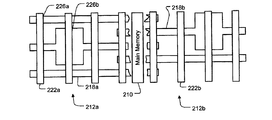
ここで、図2を参照するが、この図は、半導体メモリ装置のレベル208を示す。レベル208は、メインメモリ210とプログラマブルアドレスロジック212、214とを有する。メインメモリ210は、OTPメモリ素子216と、メモリ素子216の行に沿って延在するワードライン218と、メモリ素子216の列に沿って延在するビットライン220と、からなるクロスポイント抵抗アレイを有する。メモリ素子216の各行に対して1つのワードライン218と、メモリ素子216の各列に対して1つのビットライン220と、があってよい。各メモリ素子216は、ワードライン218とビットライン220とのクロスポイントに配置される。レベル208の図を簡略化するために、比較的少ない数のメモリ素子216のみが示されている。実際には、いかなるサイズのアレイが使用されてもよい。
【0014】
メモリラインは、ワードライン218かまたはビットライン220のいずれかを指してもよい。
【0015】
アドレスロジック212、214は、組合せダイオードロジックを使用して読出しおよび書込み動作中にメモリ素子216をアドレス指定する。アドレスロジック212、214は、ワードライン218を選択するOTP行デコーダ212を含む。行デコーダ212は、行アドレスライン222に供給されるアドレスをデコードすることによってワードライン218を選択する(アドレスは、外部行アドレスドライバ224によって供給されてもよい)。行デコーダ212は、複数のOTPアドレス素子226を有する。行デコーダ212の各アドレス素子226は、ワードライン218と行アドレスライン222とのクロスポイントにある。
【0016】
アドレスロジック212、214はまた、ビットライン220を選択するOTP列デコーダ214も有する。列デコーダ214は、列アドレスライン228に供給されるアドレスをデコードすることによりビットライン220を選択する(アドレスは、外部列アドレスドライバ230によって供給されてもよい)。列デコーダ214もまた、複数のOTPアドレス素子226を有する。列デコーダ214の各アドレス素子226は、ビットライン220と列アドレスライン228とのクロスポイントにある。
【0017】
各ワードライン218の一端は、行センスロジック234で終端する。行センスロジック234は、複数のセンス抵抗器236を有し、各センス抵抗器236は行パワーライン238とワードライン218の端部との間に接続される。行センスライン240は、ワードライン218と交差する。行センスロジック234はまた、複数のセンス素子242も有し、各センス素子242は、行センスライン240とワードライン218との間に接続される。
【0018】
各ビットライン220の一端は、列センスロジック244で終端する。列センスロジック244は、複数のセンス抵抗器236を有し、各センス抵抗器236は、列パワーライン246とビットライン220の端部との間に接続される。列センスライン248は、ビットライン220と交差する。列センスロジック244はまた、複数のセンス素子242を有し、各センス素子242は、列センスライン248とビットライン220との間に接続される。
【0019】
メインメモリ210と行デコーダ212との間の行プログラミングライン250は、ワードライン218と交差する。プログラミング素子252は、行プログラミングライン250とワードライン218との間に接続される。
【0020】
メインメモリ210と列デコーダ214との間の列プログラミングライン254は、ビットライン220と交差する。プログラミング素子252は、列プログラミングライン254とビットライン220との間に接続される。
【0021】
メモリ素子216と、アドレス素子226と、センス素子242と、プログラミング素子252と、は、すべてダイオードベースであってよい。これによって、レベル208の製作が容易になる。
【0022】
図3a乃至図3cに、異なるタイプのプログラマブル素子216/226/242/252を示す。図3aのプログラマブル素子は、ダイオード312と直列に連結されたヒューズ310を含む。プログラミングの前は、かかる素子の抵抗状態はローであり、ヒューズ310は元のまま(変化しない、intact)である。プログラミング中、素子の抵抗状態は、ヒューズ310の「飛び(blowing)」によってローからハイに変化することができる。
【0023】
図3bのプログラマブル素子は、ダイオード322と直列に連結された抵抗器320を含む。プログラミングの前は、かかる素子の抵抗状態はローであり、ヒューズ320は元のままである。プログラミング中、素子の抵抗状態は、抵抗器320の「飛び(blowing)」によりローからハイに変化することができる。
【0024】
図3cのプログラマブル素子は、ダイオード332のみを含む。プログラミングの前は、ダイオード332は元のままであるため、その抵抗状態はローである。プログラミング中、ダイオード332は、その抵抗状態をローからハイに変化させるように開放されることが可能である。かかるダイオード332は、ヒューズとして機能する。代替的に、ダイオード332は、プログラミング中に高抵抗状態から低抵抗状態になるアンチヒューズとして機能することができる。
【0025】
プログラマブル素子216/226/242/252は、図3a乃至図3cに示すタイプに限定されない。例えば、プログラマブル素子216/226/242/252は、ダイオードの代りにトランジスタを含むことができる。
【0026】
図2に戻ると、レベル208は以下のように製作することができる。基板上に列ライン220が形成され、列ライン220上にシリコンの多層膜が形成され、膜の上にワードライン218が形成される。各プログラマブル素子216/226/242/252は、2つの交差トレース(T)(図4参照)間において膜(F)のその部分として形成されてよい。プログラマブル素子216/226/242/252のサイズは、交差するライン間のオーバラップ部分と膜の厚さとによって確定される。例えば、メインメモリ210のダイオードは、交差するワードライン218とビットライン220との間において膜のその部分として形成されてよい。
【0027】
膜の異なる層は、ダイオード312、322、332を形成するために適当なドーピング(および/または結晶およびアモルファスシリコンの組合せ)を有する。抵抗器320、ヒューズ310またはアンチヒューズを形成するために、適当なドーピングにより更なる層を追加することができる。センス抵抗器236は、ワードおよびビットライン218および220の端部を変更することによって形成されてよい。行および列アドレスドライバ224および230は、基板上に制御/インタフェース回路114の一部として形成されてよい。
【0028】
データは、行および列アドレスを行および列デコーダ212および214に供給することによって、メインメモリ210に書込むことができる。書込み電流は、選択されたワードライン218と選択されたビットライン220とを流れ、したがって選択されたワードおよびビットライン218および220のクロスポイントにおいてメモリ素子216を流れる。書込み電流の大きさは、選択された要素の抵抗状態を変更するためには十分である(例えば、図3aのヒューズ310を開放すること、図3bの抵抗器320を開放すること、図3cのダイオード332を開放すること、アンチヒューズを短絡させることによる)。
【0029】
メモリ素子216の抵抗状態は、行および列デコーダ212および214に行および列アドレスを供給することによって検知することができる。行センスライン240に電圧が印加され、列センスライン248には反対の極性の電圧が印加される。センス電流は、選択されたワードライン218と選択されたビットライン220とに流れ、したがって、選択されたワードおよびビットライン218および220のクロスポイントにおいてメモリ素子216を流れる。センス電流の大きさは、選択されたメモリ素子216の抵抗状態を示す。
【0030】
ここで、図4aを参照する。行および列デコーダ212および214は、装置製作(412)前に構成されてよく(410)、レベル208が製作された後にプログラムされる(414)。デコーダ212および214は、メモリラインにアドレス構成を割当てることによって構成されてよい。各アドレス構成は、論理1と論理0とのビットパターンを含む。アドレス構成の各ビットは、メモリラインに接続されたプログラマブルアドレス素子226に対応する。アドレス素子226は、アドレス構成にしたがって製作される。例えば、「0」のアドレス構成ビット値に対応するアドレス素子226は、「1」のアドレス構成ビットに対応するアドレス素子226とは異なる通電容量を有する。ここで、アドレス素子の製作およびプログラミングをより詳細に説明する。アドレス構成を生成するアドレスプロトコルについては後述する。
【0031】
図5を参照する。塗潰しゼロ(●)によって示される高通電容量素子は、アドレス構成ビットの第1の論理値に対応する。バツ印(×)によって示される低通電容量素子は、アドレス構成ビット状態の第2の論理値に対応する。塗潰しゼロによって示されるアドレス素子226は、プログラミング中に抵抗状態が変化しない。バツ印によって示されるアドレス素子は、プログラミング中抵抗状態が変化する。単に例示の目的のために、バツ印によって示される素子は論理「0」に対応し、塗潰しゼロによって示される素子は論理「1」に対応する。論理「1」は、必ずしも高電圧に対応しない。
【0032】
行デコーダ212のプログラミング中、行プログラミングライン250にわたって電圧(−V)が印加され、行センスライン240に反対の極性の電圧(+V)が印加される。(列デコーダ214のプログラミング中、列プログラミングライン254の前後に電圧が印加され、列センスライン248に反対の極性の電圧が印加される。)これによって、背合せに接続された2つのダイオードの前後に有効に電圧が印加される。電圧は、すべてのアドレス素子が逆バイアスされ、センス素子が順方向バイアスされるように印加される。したがって、電流はアドレス素子226を流れる。この電流により、バツ印によって示されるアドレス素子226のリンクは断絶されるが、塗潰しゼロによって示されるアドレス素子226のリンクは断絶されない。このように、塗潰しゼロによって示されるアドレス素子226は元のままの(intact)状態を維持する。行デコーダ212のメモリラインM1〜M9は、元のままの(変化しない)および変化したアドレス素子226からなる異なるパターンに接続され、それによってアドレスラインのセットがメモリラインのうちの1つを除くすべてを除外することになる。
【0033】
さらに、メモリラインのダイオードパターン(プログラミング後)を示す図5aを参照する。アドレス素子226のダイオードは、ワイヤードロジック素子を形成するアクティブな素子である。アドレスラインA0〜A5にアドレスa0a1a2a3a4a5=110110が与えられると、アドレスラインA0、A1、A3およびA4に接続されたダイオードは逆バイアスされる。その結果、電流(矢印で示す)は、メモリラインからメインメモリ210に流れることができるようになる。
【0034】
同じアドレスa0a1a2a3a4a5=110110が、図5bに示すメモリラインを除外する。例えば、アドレスラインA2に論理「0」を与えると、アドレスラインA2とメモリラインとの間に接続されたダイオードが順方向バイアスされることになる。その結果、電流は順方向バイアスされたダイオードに分流し、メインメモリ210に流れなくなる。
【0035】
ここで図6a乃至図6cを参照する。高通電容量を有するアドレス素子226bは、低通電容量を有するアドレス素子226aより物理的に大型に作製される可能性がある。アドレスプロトコルが、いずれの列にも大型のアドレス素子226bが隣接していないことを保証することができる場合、アドレスロジックは、図6aに示す構成を有することができる。図6aは、列がいかなる隣接する大型のアドレス素子226bも含まない行デコーダ212を示す。そのようには示されてはいないが、アドレス素子226aおよび226bは、フルコンタクトピッチで形成されてよい。
【0036】
アドレスプロトコルがかかる保証を提供することができない場合、それによってアドレスロジックは列に隣接する大型のアドレス素子を含む可能性があるため、ワードライン218間の距離が増大する可能性がある。しかしながら、これによって、メインメモリのデータ記憶密度が低減する。
【0037】
代りに、図6bに示すように、行デコーダ212は、間隔が空けられた2つのセット212aおよび212bに分割されてよい。奇数ワードライン218aは偶数ワードライン218bと交互に噛合うように配置される。アドレスラインの第1のセット222aは、奇数ワードライン218aと交差し、アドレスラインの第2のセット222bは、偶数ワードライン218bと交差する。アドレスラインの第1および第2のセット222aおよび222bは、同じアドレス信号を受取る。
【0038】
この方法によって、隣接するアドレス素子226bのサイズは3倍に拡大されるが、それでもなお他のアドレス素子226aを高分解能で製作することができる。アドレスプロトコルが、いずれの列にも大型のアドレス素子226bが隣接していないことを保証することができる場合、隣接しない大型のメモリ素子226bのサイズを5倍に拡大することができる(図6cを参照)。
【0039】
図6a乃至図6cでは、行デコーダ212に関連して説明した。しかしながら、同じ原理を列デコーダ214に適用してよい。
【0040】
アドレスプロトコルは、nビットアドレス構成をL個のメモリライン(例えばL行またはL列)の各々に1:1にマップすることを含み、それにより、いずれの2つの行にも同じアドレス構成が割当てられず、いずれの2つの列にも同じアドレス構成が割当てられない。
【0041】
表1に示すアドレス構成を考慮する。6つのメモリラインM1〜M6と4つのアドレスラインA0〜A3とがある。アドレスラインに与えられる論理「0」は、変化しない(intact)素子によってそのアドレスラインに接続されるすべてのメモリラインを除外する。アドレスラインA0、A1、A2およびA3にアドレスa0a1a2a3=1100が供給される場合、第1のメモリラインM1を除くすべてのメモリラインM2〜M6が除外される(第1のメモリラインM1の第1および第2のアドレス素子は変化せず、第1のメモリラインの第3および第4のアドレス素子は変化する)。
【0042】
【表1】

アドレスラインは、物理的かつ電気的に層のすべての対応するアドレス素子に接続されるため、層のいずれかにおける単一の欠陥接続によって使用不可能となる場合がある。アドレスラインは、経年変化または環境プロセスにより長い間に発生する欠陥によって使用不可能となる可能性がある。アドレスラインA0、A1、A2またはA3のうちの1つが使用不可能となった場合、そのアドレスラインはいくつかのメモリラインを除外することができなくなる。アドレスラインA3に欠陥が生じると、それは、メモリラインM2、M4およびM6を除外することができなくなる。
【0044】
この問題は、耐故障性を持つアドレス構成を備えるアドレスプロトコルを使用することによって回避することができる。耐故障性は、欠陥が発生した場合であってもメモリ装置が正確に機能することができるようにする組込み冗長性を含む。このため、耐故障性は、製造歩留まりを向上させることができる。その代わり、アドレスラインが増大する。
【0045】
図7を参照する。耐故障性は、tが欠陥のあるアドレスラインの最大許容可能数である場合、少なくともt+1の対称距離を有する非包含的なアドレス構成のセットを割当てることによって達成することができる(710)。
【0046】
ここで、いくつかの条件を説明する。u1,u2∈{0,1}nとする。単方向距離dU(u1,u2)は、u1が1を有し、かつu2が0を有する位置の数である。対称距離は、dS(u1,u2)=min{dU(u1,u2),dU(u2,u1)}である。ハミング距離は、dH(u1,u2)=dU(u1,u2)+dU(u2,u1)である。ハミング距離は、対称距離の少なくとも2倍である。すなわち、dH(u1,u2)≧2dS(u1,u2)である。例えば、u1=1110およびu2=1001である場合、dU(u1,u2)=2およびdU(u2,u1)=1であり、dH(u1,u2)=3であり、dS(u1,u2)=1である。少なくとも2つのnビットワードのセットUの場合、対称距離dS(U)は、セットUにおける任意の2つの別個のワードの間における最小の対称距離であり、ハミング距離dH(U)は、セットUにおける任意の2つの別個のワードの間における最小ハミング距離である。
【0047】
dU(u1,u2)=0である場合、u2はu1を包含する。したがって、u2がu1を包含するかまたはu1がu2を包含する場合に限って、dS(u1,u2)=0である。いずれのアドレス構成も他のアドレス構成を包含しないように、メモリラインにアドレス構成が割当てられる。この制約により、単一アドレスが複数のメモリラインを選択することが無くなる。
【0048】
したがって、あるセットにおけるnビットワードが非包含的である場合、ワードのセットは、n個のアドレスラインに対するアドレス構成として割当てられてよい。
【0049】
これら制約を満足するワードの1つのセットは、t−Sperner(n,L)コードワードである。t−Sperner(n,L)コードは、dS(U)≧t+1であるように、L個のnビットワードからなるセットUである。1−Sperner(7,6)コードの例は、U={1100100,1010010,1001101,0110001,0101010,0011100}である。ハミング距離は、dH(U)=4である。アドレスラインのt=1に欠陥が生じる場合であっても、いずれのワードも他のワードを包含しない。
【0050】
アドレスワードは、t−Spernerワードのタイプである一定重みコード(constant weight code(CWC))ワードであってよい。nビットワードのセットCは、セットCの各ワードがハミング重み(w)を有しdH(C)≧2t+2である場合、CWC(n,2t+2,w)である。これら条件は、Cがt−Sperner(n,L)コードであることを意味する。
【0051】
表2のアドレス構成を考慮する。さらなる3つのアドレスライン(A4、A5およびA6)が追加されている。いかなるt=1アドレスラインが使用不可能である場合であっても、いずれのアドレス構成も他のアドレス構成を包含しない。このため、欠陥のあるアドレスラインの最大許容可能数は、t=1である。
【0052】
【表2】
アドレスラインA1が使用不可能となった場合、残りの6つのアドレスラインA0とA2〜A6とは、6つのメモリラインM1〜M6の各々を明白に選択することができるようになる。アドレスa0a2a3a4a5a6=100100がまだ、第1のメモリラインM1を除くすべてのメモリラインM2〜M6を除外する。
【0054】
メモリ装置は、隣接排反(neighborhood-disjoint)アドレス構成を生成するアドレスプロトコルを使用することによって、より高い分解能で製作することができる。かかるアドレスプロトコルは、いずれの列においても大型のアドレス素子226bが隣接していないことを保証する。
【0055】
ここで図8を参照すると、隣接排反アドレス構成は、wがコードワードの重みであり、nがアドレスラインの数であり、tが欠陥アドレスラインの最大許容可能数である場合に、不等式(2w+t+1)≦nを満足する一定重みコードワードのセットを割当てることによって生成される。
【0056】
b番目のメモリラインMbのアドレス構成をT(b)とする。アドレス指定が隣接排反である場合、T(b)とT(b+1)は、すべてのbに対して不一致となるが(disjoint)、それは隣接するアドレスは同じ位置で1を有さないということである。すなわち、すべてのbに対してT(b)∧T(b+1)=0であり、さらにT(L)∧T(1)=0である場合、アドレス指定は隣接排反である。演算子∧は、ビットに関して「AND(論理積)」を表す。
【0057】
表3に示すアドレス構成を考慮する。ハミング重みはw=3であり、アドレスラインの数はn=9であり、欠陥アドレスラインの最大許容可能数はt=1である。いずれの列においても、大型のダイオード(塗潰しゼロで表される)が隣接していない。したがって、アドレス構成は、隣接排反である。さらに、いずれか1つのアドレスラインが使用不可能である可能性があるが、それでもまだ残りのアドレスラインはメモリラインを明確に選択することができる。耐故障性と隣接排反性に対する代価は、アドレスラインの数が4から9に増大するということである。
【0058】
【表3】
表3のアドレス構成は、t−Sperner(n,L)コードから選択され、この例ではt=1、n=9およびL=6である。この隣接排反特性を満足させるために、k番目のメモリライン(Mk)に割当てられるアドレス構成は、k−1番目のメモリラインに割当てられる構成と隣接排反である残りのコードワードからランダムに選択される。残りのコードワード間に隣接排反コードワードを見つけることができない場合、k−1番目のアドレス構成は削除され、k−1番目のアドレス構成に対する別の選択が行われる。そして、k番目のアドレス構成が選択される。
【0060】
耐故障性のみ、隣接排反のみ、又は耐故障性かつ隣接排反であるかに関らず、アドレス構成は、ルックアップテーブルを使用することによってメモリラインに割当てることができる。ルックアップテーブルは、n個のアドレスラインとL個のメモリラインとを有するメモリ装置に対してnビットアドレス構成のすべてを提供することができる。しかしながら、かかるルックアップテーブルは、メモリ装置の記憶容量が増大するにしたがって非常に大きくなる可能性がある。
【0061】
図9は、n個のアドレスラインとL個のメモリラインとに対するnビットアドレス構成のシーケンスを提供するルックアップテーブルを用いる方法を示す。本方法は、ルックアップテーブルを使用して2n個のアドレスラインとL2個のメモリラインとに対するアドレス構成を生成することを含む。
【0062】
ここで図9を参照する。合計L個のブロックが形成される(910)。「最上位列」は、各ブロックの左半分を言う。「最下位列」は、各ブロックの右半分を言う。
【0063】
各ブロックの最上位列にはシーケンスが充填され、各ブロックの最上位列が同じシーケンスを含む(912)。各ブロックの最上位列のi番目のエントリは、ルックアップテーブルのi番目のエントリと等しい。
【0064】
各ブロックの最下位列にはシーケンスが充填されることで、第2のブロックのシーケンスが第1のブロックのシーケンスに関して循環的にシフトされ、第3のブロックのシーケンスが第2のブロックに関して循環的にシフトされ、と続く(914)。シーケンスは循環的にシフトされ、k番目のブロックの最下位列のi番目のエントリがルックアップテーブルの(i+s(k))番目のエントリと等しくなる。ここでs(k)は第1のブロックに対するk番目のブロックのシフトの量である。この合計がLより大きい場合、i+s(k)からLを減算しなければならない。
【0065】
Lが奇数である場合、k番目のブロックの最下位列のシフトの量s(k)は、k−1番目のブロックのシフトの量s(k−1)から2を引いたものから取得されてよい。すなわち、s(k)=s(k−1)−2である。減算の結果が負の値となる場合、Lが加算される。すなわち、s(k−1)<2である場合、s(k)=s(k−1)−2+Lである。隣接排反特性が侵されないように、s(L/2+1)の奇数値が選択される場合、(L/2+1)番目のブロックを除き、Lが偶数である場合も同じことが適用される。
【0066】
各ブロック(k)に対する循環的シフトs(k)は別個である。結果として、L個のブロックは、L2個のメモリラインと2n個のアドレスラインとに対するアドレス構成を含む。
【0067】
ここで、図9の方法の第1の実施例を提供する。表4に示すルックアップテーブルは、L=3個のメモリライン、n=3個のアドレスラインおよびt=0、1個のアドレス構成を提供する。アドレス構成はシーケンスABCを形成し、ここでA、BおよびCは、それぞれ3ビット構成001b、010bおよび100bを表す。
【0068】
図9の方法を使用して、2n=6個アドレスラインとL2=9個のメモリラインとに対する隣接排反アドレス構成を生成する。表5に示すように、各ブロックの最上位列(b0)は、同じシフトされていないシーケンス(ABC)を有し、i番目の最上位列のエントリは表4のルックアップテーブルのi番目のエントリと同じである。最下位列(b1)の各ブロックのシーケンスがシフトされる。この実施例では、s(1)=0、s(2)=1およびs(3)=2である(第1のブロックにはシフトが無く、第2のブロックではシフトが1であり、第3のブロックではシフトが2である)。このより大きいアドレス指定プロトコルに対してもまた、隣接排反特性が維持される。
【0069】
【表4】
【表5】
表6に別の実施例を提供する。シーケンスABCDは、n個のアドレスラインと4個のメモリラインとに対するL=4隣接排反アドレス構成を表す。アスタリスク(*)は、アドレス構成DおよびBが隣接排反であること、アドレス構成AおよびDが隣接排反であることを仮定する。すなわち、A∧D=0およびB∧D=0である。
【0072】
各ブロックの最上位列(b0)は、同じシーケンス(ABCD)を有し、各最上位列(b0)のi番目のエントリはシーケンスのi番目のエントリと同じである。最下位列(b1)のシーケンスは、各ブロックにおいてその相を変化させる。この実施例では、s(1)=0、s(2)=2、s(3)=3およびs(4)=1である。最後の2nビット構成が最初のビット構成から排反する以外は、このより大きいアドレス指定プロトコルにおいても隣接排反特性が維持される。
【0073】
【表6】
L=4個のメモリラインに対するアドレス構成がtまでの欠陥アドレスライン(n個のアドレスラインから)に対して耐性を有することができる場合、合計L2=16個のメモリラインが、同じ数の欠陥アドレスラインに対して耐性を有することができる。さらに、最上位列にはt個までの欠陥アドレスラインがあってよく、最下位列にはt個までの欠陥アドレスラインがあってよい。
【0075】
この実施例では、nビット構成アドレスA**が、構成アドレスDおよびAと隣接排反するnビット構成アドレスによって置換えられない限り、隣接排反特性は循環的であり続けない。
【0076】
A**を置換える代りに、「ツイン(twin)」テーブルを構成し表6に追加することができる。表7は、かかるツインテーブルである(なおB∧D=0という仮定の下にある)。表7は循環的でないが、A∧C=0である場合、隣接排反特性を侵害することなく表7を表6に追加することができる。同様に、A∧C=0である場合、表6は、その特性を侵すことなく表7に続くことができる。
【0077】
【表7】
L3個のラインのアドレス指定の場合、ここではツインテーブルは3つの列(b0、b1およびb2)を有し、図10aおよび図10bに示す構造を有する。図10aおよび図10bの各々において、右の列は、左の列に連結されている。数字1010は、表6の最初の2つの列を含むブロックを示し、数字1012は、表7の最初の2つの列を含むブロックを示す。数字1014は、4回繰返されるシーケンスABCDを示し、数字1016は、4回繰返されるシーケンスCDABを示し、数字1018は、4回繰返されるシーケンスDABCを示し、数字1020は、4回繰返されるシーケンスBCDAを示す。
【0079】
図9の方法を、L4個のメモリラインおよび4n個のアドレスライン等に拡張することができる。
【0080】
L個のメモリラインに対するオリジナルアドレスプロトコルTが隣接排反であり、さらに以下の6つの条件が満足されるように、1とLとの間にインデックスc0、c1、c2およびc3がある場合、ツインテーブルの構成と大型メモリアレイへの拡張とを行うことができる。すなわち、
(a)c0およびc1が異なるパリティを有する(整数として)
(b)c2およびc3が異なるパリティを有する(整数として)
(c)T(c0+1)∧T(c1)=0
(d)T(c1+1)∧T(c2)=0
(e)T(c2+1)∧T(c3)=0
(f)T(c3+1)∧T(c0)=0
L+1のインデックス値を、1として解釈しなければならない。このため、L=4、T(1)=A、T(2)=B、T(3)=CおよびT(4)=Dであり、かつA∧C=0かつB∧D=0である場合、
c0=1
c1=4
c2=3
c3=2
に対して条件(a)〜(f)が成り立つ。
【0081】
図9の方法は、図7および図8に示す方法によって生成される耐故障性および/または隣接排反アドレス構成の拡張に限定されない。アドレス構成は、他の方法によって同様に生成されてよい。
【0082】
上記アドレスプロトコルは、上述したメモリ装置に限定されない。それらは、組合せのアドレスロジックを使用していかなる装置に適用されてもよい。
【0083】
本発明は、上に説明し例示した特定の実施形態に限定されない。代りに、本発明は、上述した特許請求の範囲にしたがって解釈される。この発明は例として、次の実施形態を含む。
【0084】
(1)L個のメモリライン及びn個のアドレスラインを有するアドレス構成のシーケンスを使用する方法であって、
L個のブロックを形成し(910)、各ブロックの最上位列が同一のシフトされていない前記シーケンスを含むように、各ブロックの最上位列に前記シーケンスを充填し(912)、
該ブロックの最下位列のエントリが循環的にシフトされるように、各ブロックの最下位列に前記シーケンスを充填し(914)、
それにより、前記L個のブロックが、L2個のメモリラインと2n個のアドレスラインのためのアドレス構成を含む方法。
【0085】
(2)各ブロックに対する前記循環的シフトは、固有である(1)に記載の方法。
【0086】
(3)各ブロックの前記最上位列のi番目のエントリは、前記シーケンスのi番目のエントリと等しい(1)に記載の方法。
【0087】
(4)k番目のブロックの前記最下位列のi番目のエントリは、s(k)がシフトの量である場合、前記シーケンスの(i+s(k))番目のエントリと等しい(1)に記載の方法。
【0088】
(5)Lが奇数の場合、s(k)=s(k−2)−2である(4)に記載の方法。
【0089】
(6)L個のブロックは第1のテーブルを含み、Lが偶数である場合に該第1のテーブルからツインテーブルを形成することをさらに含む(1)に記載の方法。
【0090】
(7)前記第1のテーブルを、前記ツインテーブルの最後に追加する(6)に記載の方法。
【0091】
(8)前記ツインテーブルを、前記第1のテーブルの最後に追加する(6)に記載の方法。
【0092】
(9)L個のメモリラインを包含する前記シーケンスが隣接排反であり、さらに以下の6つの条件、すなわち、c0およびc1が異なるパリティを有し(整数として)、c2およびc3が異なるパリティを有し(整数として)、T(j)がj番目のメモリラインのアドレス構成である場合、T(c1+1)∧T(c2)=0であり、T(c0+1)∧T(c1)=0であり、T(c2+1)∧T(c3)=0であり、T(c3+1)∧T(c0)=0であるということが満足されるように、1とLとの間にインデックスc0、c1、c2およびc3が存在する(6)に記載の方法。
【0093】
(10)前記シーケンスもまた、請求項1記載の方法を使用して生成したものである(1)に記載の方法。
【図面の簡単な説明】
【図1】マルチレベル半導体メモリ装置の図である。
【図2】アドレスロジックを含む、半導体メモリ装置のレベルの図である。
【図3a】レベルにおける異なるタイプのプログラマブル素子の図である。
【図3b】レベルにおける異なるタイプのプログラマブル素子の図である。
【図3c】レベルにおける異なるタイプのプログラマブル素子の図である。
【図4】プログラマブル素子の他の図である。
【図4a】アドレスロジックを形成する方法の図である。
【図5】メモリラインのアドレスパターンの図である。
【図5a】メモリラインのダイオードパターンの図である。
【図5b】メモリラインのダイオードパターンの図である。
【図6a】アドレスロジックのアドレス素子の異なるレイアウトの図である。
【図6b】アドレスロジックのアドレス素子の異なるレイアウトの図である。
【図6c】アドレスロジックのアドレス素子の異なるレイアウトの図である。
【図7】アドレスロジックのためのアドレス構成を生成する第1の方法の図である。
【図8】アドレスロジックのためのアドレス構成を生成する第2の方法の図である。
【図9】ルックアップテーブルを使用してアドレスロジックのためアドレス構成を拡張する方法の図である。
【図10a】例示的なツインルックアップテーブルを示す。
【図10b】例示的なツインルックアップテーブルを示す。
【符号の説明】
210 メインメモリ
220 ビットライン
222 行アドレスライン
226 OTPアドレス素子
228 列アドレスライン
236 センス抵抗器
312,322,332 ダイオード[0001]
BACKGROUND OF THE INVENTION
The present invention relates to an information storage device. More particularly, the present invention relates to address logic for semiconductor memories.
[0002]
[Prior art]
Portable devices such as PDAs, handheld computers, digital cameras, and digital music players have memory for storing data, digital images, and MP3 files. Different types of memory are available for these portable devices. Conventional memory types include flash memory, small hard drives, small compact disks, and magnetic tape. However, each of these memory types has one or more of the following limitations. That is, the physical size is large, the storage capacity is low, the cost is relatively high, the robustness is poor, the access time is low, and the power consumption is high.
[0003]
A semiconductor diode based OTP memory is disclosed in commonly assigned US patent application Ser. No. 09 / 875,356, filed Jun. 5, 2001. Compared with a conventional memory, a diode-based memory has high impact resistance, low power consumption, high access time, moderate transfer speed, and sufficient storage capacity. The diode-based memory can be adapted to a standard portable interface (eg, PCMCIA, CF) of a portable device.
[0004]
In a diode-based memory device having multiple levels, each level has a main memory and address logic (unlike conventional semiconductor memory such as DRAM). The address logic of the diode-based memory device is programmable. The address logic can be programmed after each level is created. Since no masking is required, the physical processing is simplified.
[0005]
[Problems to be solved by the invention]
Increasing memory capacity is a continuing goal of memory manufacturers. However, as the memory capacity increases, the number of address lines and memory lines also increases. Thereby, the address configuration is lengthened to accommodate the increase in address lines, and the number of address configurations is increased to accommodate the increase in memory lines.
[0006]
An efficient generation of address configuration is required.
[0007]
[Means for Solving the Problems]
According to one aspect of the invention, the method includes using a sequence of address configurations having L memory lines and n address lines. The method forms L blocks. The top row of each block is filled with a sequence so that the top row of each block contains the same unshifted sequence. The lowest column of each block is filled with a sequence so that the entry in the lowest column of the block is cyclically shifted. L blocks are L 2 This includes an address configuration for one memory line and 2n address lines.
[0008]
Other aspects and advantages of the present invention will become apparent from the following detailed description, taken in conjunction with the accompanying drawings, illustrating by way of example the principles of the invention.
[0009]
DETAILED DESCRIPTION OF THE INVENTION
As shown in the drawings for purposes of illustration, the present invention is embodied in a diode-based OTP memory device. In the following paragraphs, the structure of the OTP memory device is described, followed by two address protocols. One of the address protocols can provide a fault-tolerant address configuration. The other address protocol can provide a neighborhood-disjoint address configuration as well as a fault tolerant address configuration. Fault-tolerant address logic can improve manufacturing yield, and adjacent reject address logic can form memory devices with higher resolution. Following the description of the address protocol, a method for extending the address configuration to a large memory array using lookup is described.
[0010]
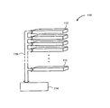
FIG. 1 shows a multilevel
[0011]
The
[0012]
If the address logic is fault tolerant, one address line may be defective at one level and another address line may be defective at another level, but each level is independent Resistant to defects.
[0013]
Reference is now made to FIG. 2, which shows a
[0014]
A memory line may refer to either the
[0015]
[0016]
The
[0017]
One end of each
[0018]
One end of each
[0019]
A
[0020]
A
[0021]
Memory element 216,
[0022]
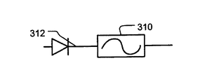
Figures 3a to 3c show different types of programmable elements 216/226/242/252. The programmable element of FIG. 3 a includes a
[0023]
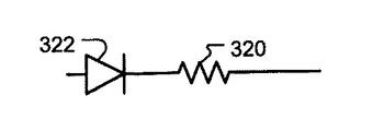
The programmable element of FIG. 3 b includes a
[0024]
The programmable element of FIG. 3 c includes only a
[0025]
The programmable elements 216/226/242/252 are not limited to the types shown in FIGS. 3a to 3c. For example, the programmable element 216/226/242/252 can include a transistor instead of a diode.
[0026]
Returning to FIG. 2, the
[0027]
Different layers of the film have appropriate doping (and / or a combination of crystalline and amorphous silicon) to form
[0028]
Data can be written to
[0029]
The resistance state of memory element 216 can be detected by supplying row and column addresses to row and
[0030]
Reference is now made to FIG. Row and
[0031]
Please refer to FIG. The high current-carrying capacitive element indicated by filled zero (●) corresponds to the first logical value of the address configuration bit. The low current-carrying capacitive element indicated by the cross (x) corresponds to the second logical value in the address configuration bit state.
[0032]
During programming of the
[0033]
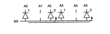
Further, reference is made to FIG. 5a showing the diode pattern of the memory line (after programming). The diode of the
[0034]
Same address a 0 a 1 a 2 a 3 a 4 a 5 = 110110 excludes the memory lines shown in FIG. 5b. For example, when a logic “0” is applied to the address line A2, a diode connected between the address line A2 and the memory line is forward-biased. As a result, current is shunted to the forward-biased diode and no longer flows to the
[0035]
Reference is now made to FIGS. 6a to 6c. The
[0036]
If the address protocol is unable to provide such a guarantee, it can increase the distance between
[0037]
Alternatively, as shown in FIG. 6b, the
[0038]
By this method, the size of the
[0039]
6a to 6c have been described in relation to the
[0040]
The address protocol includes mapping an n-bit address configuration 1: 1 to each of L memory lines (eg, L rows or L columns), thereby assigning the same address configuration to any two rows The same address configuration is not assigned to any two columns.
[0041]
Consider the address configuration shown in Table 1. There are six memory lines M1 to M6 and four address lines A0 to A3. A logic “0” applied to an address line excludes all memory lines connected to that address line by an intact element. Address a on address lines A0, A1, A2 and A3 0 a 1 a 2 a 3 = 1100 is supplied, all the memory lines M2 to M6 except the first memory line M1 are excluded (the first and second address elements of the first memory line M1 are not changed and the first The third and fourth address elements of the memory line change).
[0042]
[Table 1]
Since the address line is physically and electrically connected to all corresponding address elements of the layer, it may be disabled due to a single defective connection in any of the layers. Address lines can become unusable due to long-term defects due to aging or environmental processes. If one of the address lines A0, A1, A2 or A3 becomes unusable, the address line cannot exclude some memory lines. If the address line A3 is defective, it cannot exclude the memory lines M2, M4 and M6.
[0044]
This problem can be avoided by using an address protocol with a fault-tolerant address configuration. Fault tolerance includes built-in redundancy that allows the memory device to function correctly even if a defect occurs. For this reason, fault tolerance can improve the manufacturing yield. Instead, the address line is increased.
[0045]
Please refer to FIG. Fault tolerance can be achieved by assigning a set of non-inclusive address configurations having at least t + 1 symmetric distances, where t is the maximum allowable number of defective address lines (710).
[0046]
Here, some conditions will be described. u 1 , U 2 ∈ {0,1} n And Unidirectional distance d U (U 1 , U 2 ) U 1 Has 1 and u 2 Is the number of positions having 0. The symmetry distance is d S (U 1 , U 2 ) = Min {d U (U 1 , U 2 ), D U (U 2 , U 1 )}. Hamming distance is d H (U 1 , U 2 ) = D U (U 1 , U 2 ) + D U (U 2 , U 1 ). The Hamming distance is at least twice the symmetry distance. That is, d H (U 1 , U 2 ) ≧ 2d S (U 1 , U 2 ). For example, u 1 = 1110 and u 2 = 1001, d U (U 1 , U 2 ) = 2 and d U (U 2 , U 1 ) = 1 and d H (U 1 , U 2 ) = 3 and d S (U 1 , U 2 ) = 1. For a set U of at least two n-bit words, the symmetric distance d S (U) is the minimum symmetric distance between any two separate words in set U and the Hamming distance d H (U) is the minimum Hamming distance between any two separate words in set U.
[0047]
d U (U 1 , U 2 ) = 0, u 2 Is u 1 Is included. Therefore, u 2 Is u 1 Or u 1 Is u 2 Only if it contains S (U 1 , U 2 ) = 0. An address configuration is assigned to a memory line so that none of the address configurations includes other address configurations. This restriction prevents a single address from selecting multiple memory lines.
[0048]
Thus, if an n-bit word in a set is non-inclusive, the set of words may be assigned as an address configuration for n address lines.
[0049]
One set of words that satisfies these constraints is the t-Spnerer (n, L) codeword. t-Spener (n, L) code is d S A set U consisting of L n-bit words such that (U) ≧
[0050]
The address word may be a constant weight code (CWC) word, which is a type of t-Sperner word. A set C of n-bit words has each word of set C having a Hamming weight (w) d H When (C) ≧ 2t + 2, CWC (n, 2t + 2, w). These conditions mean that C is a t-Sperner (n, L) code.
[0051]
Consider the address configuration in Table 2. Three additional address lines (A4, A5 and A6) have been added. Even if no t = 1 address line is available, no address configuration includes other address configurations. For this reason, the maximum allowable number of defective address lines is t = 1.
[0052]
[Table 2]
When the address line A1 becomes unusable, the remaining six address lines A0 and A2 to A6 can clearly select each of the six memory lines M1 to M6. Address a 0 a 2 a 3 a 4 a 5 a 6 = 100100 still excludes all memory lines M2-M6 except for the first memory line M1.
[0054]
Memory devices can be fabricated with higher resolution by using an address protocol that generates a neighborhood-disjoint address configuration. Such an address protocol ensures that
[0055]
Referring now to FIG. 8, the adjacent reject address configuration is such that w is the codeword weight, n is the number of address lines, and t is the maximum allowable number of defective address lines. Generated by assigning a set of constant weight codewords satisfying 2w + t + 1) ≦ n.
[0056]
The address configuration of the b-th memory line Mb is T (b). If the addressing is contiguous, T (b) and T (b + 1) are disjoint for all b (disjoint), which means that adjacent addresses do not have 1 at the same position It is. That is, if T (b) ∧T (b + 1) = 0 for all b, and T (L) ∧T (1) = 0, then the addressing is adjacent exclusion. The operator ∧ represents “AND (logical product)” with respect to bits.
[0057]
Consider the address configuration shown in Table 3. The Hamming weight is w = 3, the number of address lines is n = 9, and the maximum allowable number of defective address lines is t = 1. In either row, large diodes (represented by filled zeros) are not adjacent. Therefore, the address configuration is adjacent exclusion. Further, any one address line may be unusable, but still the remaining address lines can clearly select the memory line. The price for fault tolerance and adjacent rejection is that the number of address lines increases from 4 to 9.
[0058]
[Table 3]
The address structure in Table 3 is selected from the t-Sperner (n, L) code, and in this example t = 1, n = 9 and L = 6. In order to satisfy this adjacent rejection characteristic, the address configuration assigned to the kth memory line (Mk) is randomly selected from the configuration assigned to the k−1th memory line and the remaining codewords that are adjacent rejection. Selected. If no adjacent reject codeword can be found between the remaining codewords, the k-1th address configuration is deleted and another selection is made for the k-1th address configuration. Then, the kth address configuration is selected.
[0060]
Whether fault-tolerant only, adjacent rejection only, or fault-tolerant and adjacent rejection, address configurations can be assigned to memory lines by using a look-up table. The look-up table can provide all of the n-bit address configuration for a memory device having n address lines and L memory lines. However, such a lookup table can become very large as the storage capacity of the memory device increases.
[0061]
FIG. 9 illustrates a method using a look-up table that provides a sequence of n-bit address configurations for n address lines and L memory lines. The method uses 2n address lines and L using a lookup table. 2 Generating an address configuration for the memory lines.
[0062]
Reference is now made to FIG. A total of L blocks are formed (910). “Top row” refers to the left half of each block. “Lowest column” refers to the right half of each block.
[0063]
The top row of each block is filled with a sequence, and the top row of each block contains the same sequence (912). The i-th entry in the top row of each block is equal to the i-th entry in the lookup table.
[0064]
The lowest column of each block is filled with a sequence, so that the sequence of the second block is cyclically shifted with respect to the sequence of the first block, and the sequence of the third block is cycled with respect to the second block. Shifted to (914). The sequence is cyclically shifted so that the i th entry in the lowest column of the k th block is equal to the (i + s (k)) th entry in the lookup table. Here, s (k) is the shift amount of the kth block with respect to the first block. If this sum is greater than L, L must be subtracted from i + s (k).
[0065]
When L is an odd number, the shift amount s (k) of the least significant column of the kth block is obtained from the shift amount s (k-1) of the k-1th block minus 2. May be. That is, s (k) = s (k−1) −2. If the result of the subtraction is a negative value, L is added. That is, when s (k−1) <2, s (k) = s (k−1) −2 + L. The same applies when L is even, except for the (L / 2 + 1) th block, when an odd value of s (L / 2 + 1) is selected so that the adjacent rejection characteristics are not compromised.
[0066]
The cyclic shift s (k) for each block (k) is distinct. As a result, L blocks 2 This includes an address configuration for one memory line and 2n address lines.
[0067]
Here, a first embodiment of the method of FIG. 9 is provided. The lookup table shown in Table 4 provides L = 3 memory lines, n = 3 address lines and t = 0, 1 address configuration. The address configuration forms the sequence ABC, where A, B and C are each a 3-bit configuration 001 b , 010 b And 100 b Represents.
[0068]
Using the method of FIG. 9, 2n = 6 address lines and L 2 = Adjacent reject address configuration for 9 memory lines is generated. As shown in Table 5, the most significant column (b 0 ) Have the same unshifted sequence (ABC), and the i-th most significant column entry is the same as the i-th entry in the lookup table of Table 4. The lowest column (b 1 ) The sequence of each block is shifted. In this embodiment, s (1) = 0, s (2) = 1 and s (3) = 2 (the first block has no shift, the second block has a shift of 1, 3 blocks have a shift of 2). Adjacent rejection characteristics are also maintained for this larger addressing protocol.
[0069]
[Table 4]
[Table 5]
Table 6 provides another example. The sequence ABCD represents an L = 4 adjacent reject address configuration for n address lines and 4 memory lines. The asterisk (*) assumes that address configurations D and B are adjacent rejects and address configurations A and D are adjacent rejects. That is, A∧D = 0 and B∧D = 0.
[0072]
The top row of each block (b 0 ) Have the same sequence (ABCD) and each top row (b 0 ) Is the same as the i-th entry in the sequence. The lowest column (b 1 ) Sequence changes its phase in each block. In this example, s (1) = 0, s (2) = 2, s (3) = 3 and s (4) = 1. Adjacent rejection characteristics are maintained in this larger addressing protocol, except that the last 2n bit configuration is rejected from the initial bit configuration.
[0073]
[Table 6]
If the address configuration for L = 4 memory lines can be tolerant to defective address lines (from n address lines) up to t, then total L 2 = 16 memory lines can be tolerant to the same number of defective address lines. Furthermore, there may be up to t defective address lines in the top column and up to t defective address lines in the bottom column.
[0075]
In this embodiment, the adjacent rejection characteristic does not continue to be cyclic unless the n-bit configuration address A ** is replaced by an n-bit configuration address that is adjacent to the configuration addresses D and A.
[0076]
Instead of replacing A **, a “twin” table can be constructed and added to Table 6. Table 7 is such a twin table (still under the assumption that B∧D = 0). Table 7 is not circular, but if A∧C = 0, Table 7 can be added to Table 6 without violating the adjacent rejection characteristics. Similarly, if A∧C = 0, Table 6 can continue to Table 7 without violating its properties.
[0077]
[Table 7]
L 3 In the case of addressing a single line, the twin table here has three columns (b 0 , B 1 And b 2 And the structure shown in FIGS. 10a and 10b. In each of FIGS. 10a and 10b, the right column is connected to the left column. The numeral 1010 indicates a block including the first two columns of Table 6, and the numeral 1012 indicates a block including the first two columns of Table 7. The
[0079]
The method of FIG. 4 The number of memory lines can be expanded to 4n address lines.
[0080]
An index c between 1 and L so that the original address protocol T for L memory lines is adjacent and the following six conditions are satisfied: 0 , C 1 , C 2 And c 3 If there is, a twin table configuration and expansion to a large memory array can be performed. That is,
(A) c 0 And c 1 Have different parity (as integers)
(B) c 2 And c 3 Have different parity (as integers)
(C) T (c 0 +1) ∧T (c 1 ) = 0
(D) T (c 1 +1) ∧T (c 2 ) = 0
(E) T (c 2 +1) ∧T (c 3 ) = 0
(F) T (c 3 +1) ∧T (c 0 ) = 0
The L + 1 index value must be interpreted as 1. Therefore, L = 4, T (1) = A, T (2) = B, T (3) = C and T (4) = D, and A∧C = 0 and B∧D = 0. If there is
c 0 = 1
c 1 = 4
c 2 = 3
c 3 = 2
The conditions (a) to (f) are satisfied.
[0081]
The method of FIG. 9 is not limited to the fault tolerance and / or adjacent reject address configuration extensions generated by the methods shown in FIGS. The address configuration may be similarly generated by other methods.
[0082]
The address protocol is not limited to the memory device described above. They may be applied to any device using a combination of address logic.
[0083]
The present invention is not limited to the specific embodiments described and illustrated above. Instead, the present invention is construed according to the claims that follow. The present invention includes the following embodiment as an example.
[0084]
(1) A method of using an address configuration sequence having L memory lines and n address lines,
L blocks are formed (910), and the top row of each block is filled with the sequence so that the top row of each block contains the same unshifted sequence (912),
Filling the sequence in the lowest column of each block (914) so that the entries in the lowest column of the block are cyclically shifted;
As a result, the L blocks become L 2 A method including an address configuration for 2 memory lines and 2n address lines.
[0085]
(2) The method according to (1), wherein the cyclic shift for each block is unique.
[0086]
(3) The method according to (1), wherein the i-th entry in the highest column of each block is equal to the i-th entry in the sequence.
[0087]
(4) The i-th entry in the lowest column of the k-th block is equal to (1) when the s (k) is the shift amount, and is equal to the (i + s (k))-th entry of the sequence. The method described.
[0088]
(5) The method according to (4), wherein when L is an odd number, s (k) = s (k−2) −2.
[0089]
(6) The method according to (1), wherein the L blocks include a first table, and further includes forming a twin table from the first table when L is an even number.
[0090]
(7) The method according to (6), wherein the first table is added to the end of the twin table.
[0091]
(8) The method according to (6), wherein the twin table is added to the end of the first table.
[0092]
(9) The sequence including L memory lines is adjacent exclusion, and further, the following six conditions are satisfied: c 0 And c 1 Have different parity (as integers), c 2 And c 3 Have different parities (as integers) and T (j) is the address configuration of the jth memory line, T (c 1 +1) ∧T (c 2 ) = 0 and T (c 0 +1) ∧T (c 1 ) = 0 and T (c 2 +1) ∧T (c 3 ) = 0 and T (c 3 +1) ∧T (c 0 ) = 0 so that it is satisfied that the index c is between 1 and L 0 , C 1 , C 2 And c 3 The method according to (6), wherein:
[0093]
(10) The method according to (1), wherein the sequence is also generated using the method according to
[Brief description of the drawings]
FIG. 1 is a diagram of a multilevel semiconductor memory device.
FIG. 2 is a level diagram of a semiconductor memory device including address logic.
FIG. 3a is a diagram of different types of programmable elements at a level.
FIG. 3b is a diagram of different types of programmable elements at level.
FIG. 3c is a diagram of different types of programmable elements at a level.
FIG. 4 is another view of a programmable element.
FIG. 4a is a diagram of a method of forming address logic.
FIG. 5 is a diagram of an address pattern of a memory line.
FIG. 5a is a diagram of a diode pattern of a memory line.
FIG. 5b is a diagram of a diode pattern of a memory line.
FIG. 6a is a diagram of different layouts of address elements of address logic.
FIG. 6b is a diagram of different layouts of address elements of the address logic.
FIG. 6c is a diagram of different layouts of address elements of the address logic.
FIG. 7 is a diagram of a first method for generating an address configuration for address logic.
FIG. 8 is a diagram of a second method for generating an address configuration for address logic.
FIG. 9 is a diagram of a method for extending an address configuration for address logic using a lookup table.
FIG. 10a shows an exemplary twin look-up table.
FIG. 10b shows an exemplary twin look-up table.
[Explanation of symbols]
210 Main memory
220 bit lines
222 row address line
226 OTP address element
228 column address line
236 sense resistor
312,322,332 diode
Claims (19)
L個のブロックを形成することを含み、該ブロックのそれぞれの最上位列が、前記第2のアドレス素子が隣接排反して同一のシフトされていない前記シーケンスを含むように、前記シーケンスで充填されており、
前記ブロックのそれぞれの最下位列のエントリが、前記第2のアドレス素子が隣接排反して循環的にシフトされるように、前記各ブロックの最下位列が前記シーケンスで充填されており、
それにより、前記L個のブロックが、L2個のメモリラインと2n個のアドレスラインのためのアドレス構成を含む、方法。 Look including L number of memory lines and n address lines, the second address having a first address element having a first resistance state, the second resistance state large than the first address element A method of using a sequence of address configurations comprising elements ,
Forming L blocks, each topmost column of the blocks being filled with the sequence such that the second address element includes the same unshifted sequence with adjacent displacement And
The lowest column of each block is filled with the sequence so that the entry of each lowest column of the block is cyclically shifted with the second address element being adjacently displaced ;
Thereby, the L block includes address configuration for L 2 two memory lines and 2n-number of address lines, the method.
L個のメモリライン及びn個のアドレスラインのためのアドレス構成のシーケンスにアクセスするステップと、
L個のブロックを形成するステップと、を含み、
該ブロックのそれぞれの最上位列においては、前記第2のアドレス素子が隣接排反していると共に、該最上位列のi番目のエントリが前記シーケンスのi番目のエントリと等しく、k番目のブロックの最下位列においては、前記第2のアドレス素子が隣接排反していると共に、該最下位列のi番目のエントリが前記シーケンスの(i+s(k))番目のエントリと等しく(但しs(k)はシフト量)、
前記L個のブロックが、L 2 個のメモリラインと2n個のアドレスラインのためのアドレス構成を含む、方法。A method for generating an address configuration of a memory device including a first address element having a first resistance state and a second address element having a second resistance state that is larger than the first address element and having a second resistance state There,
Accessing a sequence of address configurations for L memory lines and n address lines;
Forming L blocks, and
In each uppermost column of the block, the second address elements are adjacent to each other, and the i-th entry of the uppermost column is equal to the i-th entry of the sequence, and the k-th block in the lowest column, together with the second address element is adjacent disjoint, outermost lower row i-th entry of the sequence (i + s (k)) th entry and rather equal (although s (k) is the shift amount),
The L block includes address configuration for L 2 two memory lines and 2n-number of address lines, the method.
L個のブロックを形成することを含み、該ブロックのそれぞれの最上位列においては、前記第2のアドレス素子が隣接排反していると共に、該最上位列のi番目のエントリが前記シーケンスのi番目のエントリと等しく、k番目のブロックの最下位列においては、前記第2のアドレス素子が隣接排反していると共に、該最下位列のi番目のエントリが前記シーケンスの(i+s(k))番目のエントリと等しく(但しs(k)はシフト量)、
前記L個のブロックが、L 2 個のメモリラインと2n個のアドレスラインのためのアドレス構成を含む、
方法。Using a look-up table including an address configuration for L memory lines and n address lines, a first address element having a first resistance state and a larger and first address element than the first address element. A method of generating an address configuration of a memory device including a second address element having two resistance states ,
Forming L blocks, and in each uppermost column of the block , the second address elements are adjacent to each other and the i-th entry of the uppermost column is the i of the sequence. In the lowest column of the k-th block , the second address elements are adjacent to each other and the i-th entry of the lowest column is the (i + s (k )) th entry and rather equal (but s (k) is the shift amount),
The L blocks include an address configuration for L 2 memory lines and 2n address lines;
Method.
Applications Claiming Priority (2)
| Application Number | Priority Date | Filing Date | Title |
|---|---|---|---|
| US09/990,924 | 2001-11-13 | ||
| US09/990,924 US6466512B1 (en) | 2001-11-13 | 2001-11-13 | Method of generating address configurations for solid state memory |
Publications (3)
| Publication Number | Publication Date |
|---|---|
| JP2003187589A JP2003187589A (en) | 2003-07-04 |
| JP2003187589A5 JP2003187589A5 (en) | 2005-08-04 |
| JP4081350B2 true JP4081350B2 (en) | 2008-04-23 |
Family
ID=25536657
Family Applications (1)
| Application Number | Title | Priority Date | Filing Date |
|---|---|---|---|
| JP2002323686A Expired - Fee Related JP4081350B2 (en) | 2001-11-13 | 2002-11-07 | Method for generating an address configuration for a memory |
Country Status (6)
| Country | Link |
|---|---|
| US (1) | US6466512B1 (en) |
| EP (1) | EP1310960A3 (en) |
| JP (1) | JP4081350B2 (en) |
| KR (1) | KR20030040101A (en) |
| CN (1) | CN100380518C (en) |
| TW (1) | TW580711B (en) |
Families Citing this family (13)
| Publication number | Priority date | Publication date | Assignee | Title |
|---|---|---|---|---|
| US6535455B1 (en) * | 2001-10-13 | 2003-03-18 | Hewlett-Packard Company | Fault-tolerant neighborhood-disjoint address logic for solid state memory |
| US7003713B2 (en) * | 2002-05-16 | 2006-02-21 | Broadcom Corporation | Variable Hamming error correction for a one-time-programmable-ROM |
| US7350132B2 (en) * | 2003-09-10 | 2008-03-25 | Hewlett-Packard Development Company, L.P. | Nanoscale interconnection interface |
| US7191380B2 (en) * | 2003-09-10 | 2007-03-13 | Hewlett-Packard Development Company, L.P. | Defect-tolerant and fault-tolerant circuit interconnections |
| US7307345B2 (en) * | 2005-11-01 | 2007-12-11 | Hewlett-Packard Development Company, L.P. | Crossbar-array designs and wire addressing methods that tolerate misalignment of electrical components at wire overlap points |
| WO2006137833A1 (en) * | 2004-08-13 | 2006-12-28 | University Of Florida Research Foundation, Inc. | Nanoscale content-addressable memory |
| US7489583B2 (en) * | 2005-09-06 | 2009-02-10 | Hewlett-Packard Development Company, L.P. | Constant-weight-code-based addressing of nanoscale and mixed microscale/nanoscale arrays |
| US7319416B2 (en) * | 2006-01-30 | 2008-01-15 | Hewlett-Packard Development Company, L.P. | Tunneling-resistor-junction-based microscale/nanoscale demultiplexer arrays |
| US7763978B2 (en) * | 2007-03-28 | 2010-07-27 | Hewlett-Packard Development Company, L.P. | Three-dimensional crossbar array systems and methods for writing information to and reading information stored in three-dimensional crossbar array junctions |
| US7630246B2 (en) * | 2007-06-18 | 2009-12-08 | Micron Technology, Inc. | Programming rate identification and control in a solid state memory |
| KR100892673B1 (en) | 2007-09-05 | 2009-04-15 | 주식회사 하이닉스반도체 | Circuit for Replacing Address and Semiconductor Memory Apparatus with the Same |
| KR100956946B1 (en) * | 2008-04-16 | 2010-05-11 | 매그나칩 반도체 유한회사 | Method for programming nonvolatile memory device |
| KR100971654B1 (en) * | 2008-06-25 | 2010-07-22 | (주)아이엘전자 | Flux proof tact switch |
Family Cites Families (12)
| Publication number | Priority date | Publication date | Assignee | Title |
|---|---|---|---|---|
| US4064558A (en) * | 1976-10-22 | 1977-12-20 | General Electric Company | Method and apparatus for randomizing memory site usage |
| US4092665A (en) * | 1976-12-29 | 1978-05-30 | Xerox Corporation | Method and means for extracting variable length data from fixed length bytes |
| US4556960A (en) * | 1982-12-13 | 1985-12-03 | Sperry Corporation | Address sequencer for overwrite avoidance |
| US4782340A (en) * | 1986-08-22 | 1988-11-01 | Energy Conversion Devices, Inc. | Electronic arrays having thin film line drivers |
| US5550782A (en) * | 1991-09-03 | 1996-08-27 | Altera Corporation | Programmable logic array integrated circuits |
| JPH0696598A (en) * | 1992-07-10 | 1994-04-08 | Texas Instr Japan Ltd | Semiconductor memory and defective memory cell relieving circuit |
| US5721498A (en) * | 1995-12-11 | 1998-02-24 | Hewlett Packard Company | Block segmentation of configuration lines for fault tolerant programmable logic device |
| US6172933B1 (en) * | 1998-09-04 | 2001-01-09 | Intel Corporation | Redundant form address decoder for memory system |
| KR100326268B1 (en) * | 1998-10-28 | 2002-05-09 | 박종섭 | Decoding device for taking driving margin at decoding and its method |
| JP2000285694A (en) * | 1999-03-30 | 2000-10-13 | Mitsubishi Electric Corp | Semiconductor memory and semiconductor integrated circuit mounting semiconductor memory |
| US6088287A (en) * | 1999-08-23 | 2000-07-11 | Advanced Micro Devices, Inc. | Flash memory architecture employing three layer metal interconnect for word line decoding |
| US6459648B1 (en) * | 2001-10-13 | 2002-10-01 | Josh N. Hogan | Fault-tolerant address logic for solid state memory |
-
2001
- 2001-11-13 US US09/990,924 patent/US6466512B1/en not_active Expired - Lifetime
-
2002
- 2002-10-29 TW TW091132102A patent/TW580711B/en not_active IP Right Cessation
- 2002-11-07 JP JP2002323686A patent/JP4081350B2/en not_active Expired - Fee Related
- 2002-11-12 KR KR1020020069929A patent/KR20030040101A/en not_active Application Discontinuation
- 2002-11-13 EP EP02257803A patent/EP1310960A3/en not_active Withdrawn
- 2002-11-13 CN CNB021495300A patent/CN100380518C/en not_active Expired - Lifetime
Also Published As
| Publication number | Publication date |
|---|---|
| KR20030040101A (en) | 2003-05-22 |
| TW200300261A (en) | 2003-05-16 |
| EP1310960A3 (en) | 2005-01-12 |
| CN1419240A (en) | 2003-05-21 |
| CN100380518C (en) | 2008-04-09 |
| TW580711B (en) | 2004-03-21 |
| JP2003187589A (en) | 2003-07-04 |
| EP1310960A2 (en) | 2003-05-14 |
| US6466512B1 (en) | 2002-10-15 |
Similar Documents
| Publication | Publication Date | Title |
|---|---|---|
| JP4081350B2 (en) | Method for generating an address configuration for a memory | |
| US6990622B2 (en) | Method for error correction decoding in an MRAM device (historical erasures) | |
| US7107507B2 (en) | Magnetoresistive solid-state storage device and data storage methods for use therewith | |
| JP4939528B2 (en) | Decoding circuit for non-binary group of memory line drivers | |
| US7149948B2 (en) | Manufacturing test for a fault tolerant magnetoresistive solid-state storage device | |
| US6973604B2 (en) | Allocation of sparing resources in a magnetoresistive solid-state storage device | |
| KR101224295B1 (en) | Nanoscale interconnection interface | |
| US6587394B2 (en) | Programmable address logic for solid state diode-based memory | |
| US7944729B2 (en) | Simultaneously writing multiple addressable blocks of user data to a resistive sense memory cell array | |
| US20080212352A1 (en) | Multi-layer semiconductor memory device comprising error checking and correction (ecc) engine and related ecc method | |
| EP1665276A2 (en) | Defect-tolerant and fault-tolerant circuit interconnections | |
| US6744681B2 (en) | Fault-tolerant solid state memory | |
| US6459648B1 (en) | Fault-tolerant address logic for solid state memory | |
| US20030172339A1 (en) | Method for error correction decoding in a magnetoresistive solid-state storage device | |
| JP4121825B2 (en) | Fault tolerant adjacent reject address logic | |
| JP7017495B2 (en) | How to manage flash memory | |
| US20040141389A1 (en) | Solid state storage device and data storage method | |
| EP1286360A2 (en) | Manufacturing test for a fault tolerant magnetoresistive solid-state storage device |
Legal Events
| Date | Code | Title | Description |
|---|---|---|---|
| A521 | Request for written amendment filed |
Free format text: JAPANESE INTERMEDIATE CODE: A523 Effective date: 20050106 |
|
| A621 | Written request for application examination |
Free format text: JAPANESE INTERMEDIATE CODE: A621 Effective date: 20050106 |
|
| A977 | Report on retrieval |
Free format text: JAPANESE INTERMEDIATE CODE: A971007 Effective date: 20070821 |
|
| A131 | Notification of reasons for refusal |
Free format text: JAPANESE INTERMEDIATE CODE: A131 Effective date: 20070904 |
|
| A521 | Request for written amendment filed |
Free format text: JAPANESE INTERMEDIATE CODE: A523 Effective date: 20071009 |
|
| TRDD | Decision of grant or rejection written | ||
| A01 | Written decision to grant a patent or to grant a registration (utility model) |
Free format text: JAPANESE INTERMEDIATE CODE: A01 Effective date: 20080205 |
|
| A61 | First payment of annual fees (during grant procedure) |
Free format text: JAPANESE INTERMEDIATE CODE: A61 Effective date: 20080208 |
|
| FPAY | Renewal fee payment (event date is renewal date of database) |
Free format text: PAYMENT UNTIL: 20110215 Year of fee payment: 3 |
|
| R150 | Certificate of patent or registration of utility model |
Ref document number: 4081350 Country of ref document: JP Free format text: JAPANESE INTERMEDIATE CODE: R150 Free format text: JAPANESE INTERMEDIATE CODE: R150 |
|
| FPAY | Renewal fee payment (event date is renewal date of database) |
Free format text: PAYMENT UNTIL: 20110215 Year of fee payment: 3 |
|
| S111 | Request for change of ownership or part of ownership |
Free format text: JAPANESE INTERMEDIATE CODE: R313113 |
|
| FPAY | Renewal fee payment (event date is renewal date of database) |
Free format text: PAYMENT UNTIL: 20110215 Year of fee payment: 3 |
|
| R350 | Written notification of registration of transfer |
Free format text: JAPANESE INTERMEDIATE CODE: R350 |
|
| R250 | Receipt of annual fees |
Free format text: JAPANESE INTERMEDIATE CODE: R250 |
|
| FPAY | Renewal fee payment (event date is renewal date of database) |
Free format text: PAYMENT UNTIL: 20120215 Year of fee payment: 4 |
|
| FPAY | Renewal fee payment (event date is renewal date of database) |
Free format text: PAYMENT UNTIL: 20120215 Year of fee payment: 4 |
|
| FPAY | Renewal fee payment (event date is renewal date of database) |
Free format text: PAYMENT UNTIL: 20120215 Year of fee payment: 4 |
|
| FPAY | Renewal fee payment (event date is renewal date of database) |
Free format text: PAYMENT UNTIL: 20120215 Year of fee payment: 4 |
|
| FPAY | Renewal fee payment (event date is renewal date of database) |
Free format text: PAYMENT UNTIL: 20120215 Year of fee payment: 4 |
|
| FPAY | Renewal fee payment (event date is renewal date of database) |
Free format text: PAYMENT UNTIL: 20130215 Year of fee payment: 5 |
|
| R250 | Receipt of annual fees |
Free format text: JAPANESE INTERMEDIATE CODE: R250 |
|
| FPAY | Renewal fee payment (event date is renewal date of database) |
Free format text: PAYMENT UNTIL: 20140215 Year of fee payment: 6 |
|
| R250 | Receipt of annual fees |
Free format text: JAPANESE INTERMEDIATE CODE: R250 |
|
| R250 | Receipt of annual fees |
Free format text: JAPANESE INTERMEDIATE CODE: R250 |
|
| R250 | Receipt of annual fees |
Free format text: JAPANESE INTERMEDIATE CODE: R250 |
|
| R250 | Receipt of annual fees |
Free format text: JAPANESE INTERMEDIATE CODE: R250 |
|
| R250 | Receipt of annual fees |
Free format text: JAPANESE INTERMEDIATE CODE: R250 |
|
| R250 | Receipt of annual fees |
Free format text: JAPANESE INTERMEDIATE CODE: R250 |
|
| R250 | Receipt of annual fees |
Free format text: JAPANESE INTERMEDIATE CODE: R250 |
|
| R250 | Receipt of annual fees |
Free format text: JAPANESE INTERMEDIATE CODE: R250 |
|
| R250 | Receipt of annual fees |
Free format text: JAPANESE INTERMEDIATE CODE: R250 |
|
| LAPS | Cancellation because of no payment of annual fees |