JP4068594B2 - Flash memory controller, flash memory system, and flash memory control method - Google Patents
Flash memory controller, flash memory system, and flash memory control method Download PDFInfo
- Publication number
- JP4068594B2 JP4068594B2 JP2004172262A JP2004172262A JP4068594B2 JP 4068594 B2 JP4068594 B2 JP 4068594B2 JP 2004172262 A JP2004172262 A JP 2004172262A JP 2004172262 A JP2004172262 A JP 2004172262A JP 4068594 B2 JP4068594 B2 JP 4068594B2
- Authority
- JP
- Japan
- Prior art keywords
- address
- data
- flash memory
- buffer
- physical
- Prior art date
- Legal status (The legal status is an assumption and is not a legal conclusion. Google has not performed a legal analysis and makes no representation as to the accuracy of the status listed.)
- Expired - Fee Related
Links
Images


Description
本発明は、フラッシュメモリコントローラと、フラッシュメモリシステム、及びフラッシュメモリの制御方法に関する。 The present invention includes a flash memory controller, flash memory systems, and a control method of a flash memory.
近年、メモリーカードやシリコンディスクといったメモリシステムにて使用される半導体メモリに、フラッシュメモリが広く採用されている。フラッシュメモリは、不揮発性メモリの一種である。フラッシュメモリに格納されたデータは、電力が供給されていないときでも保持されていることが要求される。 In recent years, flash memories have been widely adopted as semiconductor memories used in memory systems such as memory cards and silicon disks. A flash memory is a kind of nonvolatile memory. Data stored in the flash memory is required to be retained even when power is not supplied.
NAND型フラッシュメモリは、上記のメモリシステムで特に多く用いられるフラッシュメモリの一種である。NAND型フラッシュメモリに含まれている複数のメモリセルのそれぞれは、他のメモリセルとは独立して、論理値“1”を示すデータが格納されている消去状態から、論理値“0”を示すデータが格納されている書込状態へと変化することができる。 A NAND flash memory is a type of flash memory that is particularly frequently used in the above memory system. Each of the plurality of memory cells included in the NAND flash memory receives a logical value “0” from an erased state in which data indicating a logical value “1” is stored, independently of the other memory cells. It is possible to change to a writing state in which the indicated data is stored.
これとは対照的に、複数のメモリセルのうちの少なくとも1つが書込状態から消去状態へと変化しなければならないときには、各メモリセルは他のメモリセルと独立して変化することができない。このときには、ブロックと称される予め定められた数のメモリセルにおいて、全てのメモリセルが同時に消去状態とならなければならない。この一括消去動作は、一般的に、“ブロック消去”と称されている。 In contrast, when at least one of the plurality of memory cells must change from a written state to an erased state, each memory cell cannot change independently of the other memory cells. At this time, in a predetermined number of memory cells called blocks, all the memory cells must be simultaneously erased. This batch erase operation is generally called “block erase”.
フラッシュメモリが上記のような特徴を有しているのは、コンピュータシステムにおいてフラッシュメモリがハードディスクドライブ(HDD)と同様に取り扱われることが想定されていたからである。この特徴を有するフラッシュメモリを採用したフラッシュメモリシステムは、通常、ATA(Advanced Technology Attachment)といったHDDの規格に準拠している。従って、上記のフラッシュメモリがホストコンピュータに接続されたコンピュータシステムでは、ホストコンピュータがフラッシュメモリシステムを通常のHDDと同じように取り扱っている。 The reason why the flash memory has the above-described characteristics is that it is assumed that the flash memory is handled in the same manner as a hard disk drive (HDD) in a computer system. A flash memory system employing a flash memory having this feature generally conforms to an HDD standard such as ATA (Advanced Technology Attachment). Therefore, in the computer system in which the flash memory is connected to the host computer, the host computer handles the flash memory system in the same way as a normal HDD.
しかしながら、HDDの規格に準拠したフラッシュメモリシステムは、HDDのためのインターフェースを有していないホストコンピュータに接続することができない。フラッシュメモリを制御するための制御回路がフラッシュメモリ自身とは独立しているときには、その制御回路をホストコンピュータのメモリインタフェースに装着することが便利な場合もある。 However, a flash memory system compliant with the HDD standard cannot be connected to a host computer that does not have an interface for the HDD. When the control circuit for controlling the flash memory is independent of the flash memory itself, it may be convenient to attach the control circuit to the memory interface of the host computer.
また、データ転送が行われていないときに外部バスからの指示に応じて外部から直接揮発性メモリへアクセスしているような擬似的アクセスを可能にするコントローラが開示されいる。(例えば、特許文献1参照)。
この文献に開示されているコントローラは、フラッシュメモリから読み出されたデータをRAMに記憶できるようにし、そのRAMは、NAND型フラッシュメモリにおける数ページに対応した記憶容量を有している。これに対して、ホストコンピュータからフラッシュメモリへの柔軟なアクセスを可能とする、より簡単な構成が求められている。 The controller disclosed in this document enables data read from the flash memory to be stored in the RAM, and the RAM has a storage capacity corresponding to several pages in the NAND flash memory. On the other hand, there is a need for a simpler configuration that allows flexible access to the flash memory from the host computer.
本発明は、上記実状に鑑みてなされたもので、ホストコンピュータのメモリインタフェースに装着可能なフラッシュメモリコントローラと、フラッシュメモリシステム、及びフラッシュメモリの制御方法を提供することを目的とする。 The present invention has been made in view of the above circumstances, and an object thereof is to provide a memory interface can be mounted flash memory controller of the host computer, flash memory systems, and the control method of a flash memory.
上記目的を達成するため、本発明の第1の観点に係るフラッシュメモリコントローラは、
複数個の物理ページを含む物理ブロック単位で記憶データの消去が行われるフラッシュメモリに対するアクセスを制御するメモリコントローラであって、
前記フラッシュメモリに書き込むデータ又は前記フラッシュメモリから読み出されたデータを保持する手段であって、ホストシステムのメモリアドレス空間に割り当てられているバッファと、
ホストシステム側から、該ホストシステムのメモリアドレス空間におけるアクセス単位で、前記バッファにランダムアクセスできるように制御し、さらに、前記ホストシステム側から与えられる複数ビットのアドレスを所定の上位側ビットと下位側ビットに分離し、該上位側ビットに基づいて前記バッファに保持されているデータがアクセス対象のデータに該当するか否かを判別し、該下位側ビットに基づいて前記バッファ内のアクセス領域を識別するホストインタフェース制御手段と、
前記ホストシステム側から与えられるアクセス対象の論理ページを特定するための論理ページアドレスが保持されるアドレス保持手段と、
複数の前記論理ページを含む論理ブロックに付けられたアドレスである論理ブロックアドレスと、前記物理ブロックに付けられたアドレスである物理ブロックアドレスとの対応関係を管理するアドレス管理手段と、
前記アドレス保持手段に保持されている前記論理ページアドレスの前記論理ブロックアドレスに対応する所定の上位側ビット部分を、該論理ブロックアドレスと対応する前記物理ブロックアドレスに置き換えた物理ページアドレスを生成するアドレス生成手段と、
前記アドレス生成手段によって生成された前記物理ページアドレスに対応する前記物理ページにデータを書き込むための前記バッファから前記フラッシュメモリへの512バイト単位のデータ転送と、前記アドレス生成手段によって生成された前記物理ページアドレスに対応する前記物理ページからデータを読み出すための前記フラッシュメモリから前記バッファへの512バイト単位のデータ転送とを制御するフラッシュメモリインタフェース制御手段と、
を備えることを特徴とする。
In order to achieve the above object, a flash memory controller according to a first aspect of the present invention includes:
A memory controller for controlling access to a flash memory in which stored data is erased in units of physical blocks including a plurality of physical pages,
Means for holding data to be written to the flash memory or data read from the flash memory, and a buffer assigned to a memory address space of a host system;
From the host system side, control is performed so that the buffer can be randomly accessed in an access unit in the memory address space of the host system. Further, a plurality of bits given from the host system side are assigned a predetermined upper bit and lower side. It is divided into bits, and it is determined whether the data held in the buffer corresponds to the data to be accessed based on the upper bit, and the access area in the buffer is identified based on the lower bit and host Inn tough Esu control means for,
Address holding means for holding a logical page address for specifying a logical page to be accessed given from the host system side;
Address management means for managing a correspondence relationship between a logical block address that is an address attached to a logical block including a plurality of the logical pages and a physical block address that is an address attached to the physical block;
An address for generating a physical page address in which a predetermined upper bit portion corresponding to the logical block address of the logical page address held in the address holding means is replaced with the physical block address corresponding to the logical block address Generating means;
512-byte data transfer from the buffer to the flash memory for writing data to the physical page corresponding to the physical page address generated by the address generating means, and the physical generated by the address generating means Flash memory interface control means for controlling data transfer in units of 512 bytes from the flash memory to the buffer for reading data from the physical page corresponding to a page address;
It is characterized by providing.
また、この発明の第2の観点に係るフラッシュメモリシステムは、上述のメモリコントローラと、物理ブロック単位で記憶データの消去が行われるフラッシュメモリとを備えることを特徴とする。A flash memory system according to a second aspect of the present invention includes the above-described memory controller and a flash memory in which stored data is erased in units of physical blocks.
上記目的を達成するため、本発明の第3の観点に係るフラッシュメモリの制御方法は、
複数個の物理ページを含む物理ブロック単位で記憶データの消去が行われるフラッシュメモリに対するアクセスを制御するフラッシュメモリの制御方法であって、
アクセス対象の論理ページを特定するための論理ページアドレスが保持されるアドレス保持手段に、ホストシステム側から与えられる複数ビットの前記論理ページアドレスを保持する論理ページアドレス保持ステップと、
複数の前記論理ページを含む論理ブロックに付けられたアドレスである論理ブロックアドレスと、前記物理ブロックに付けられたアドレスである物理ブロックアドレスとの対応関係を管理するアドレス管理ステップと、
前記アドレス保持手段に保持されている前記論理ページアドレスの前記論理ブロックアドレスに対応する所定の上位側ビット部分を、該論理ブロックアドレスと対応する前記物理ブロックアドレスに置き換えた物理ページアドレスを生成するアドレス生成ステップと、
512バイトの転送単位で、前記アドレス生成ステップで生成された前記物理ページアドレスに対応する前記物理ページに書き込まれるデータ又は前記アドレス生成ステップで生成された前記物理ページアドレスに対応する前記物理ページから読み出されたデータを保持するバッファと前記フラッシュメモリとの間でのデータ転送を制御するデータ転送ステップと、
ホストシステム側から与えられる複数ビットのアドレスを所定の上位側ビットと下位側ビットに分離し、前記上位側ビットに基づいて、前記バッファに保持されているデータがアクセス対象のデータに該当するか否かを判別し、前記下位側ビットに基づいて前記バッファ内のアクセス領域を識別する識別ステップと、
前記ホストシステム側から、該ホストシステムのメモリアドレス空間におけるアクセス単位で、前記バッファにランダムアクセスできるように制御するアクセス制御ステップとを有し、
前記バッファは、前記ホストシステムのメモリアドレス空間に割り当てられていることを特徴とする。
In order to achieve the above object, a flash memory control method according to a third aspect of the present invention includes:
A flash memory control method for controlling access to a flash memory in which stored data is erased in units of physical blocks including a plurality of physical pages ,
A logical page address holding step for holding a plurality of bits of the logical page address given from the host system side in an address holding means for holding a logical page address for specifying a logical page to be accessed ;
An address management step for managing a correspondence relationship between a logical block address that is an address attached to a logical block including a plurality of the logical pages and a physical block address that is an address attached to the physical block;
An address for generating a physical page address in which a predetermined upper bit portion corresponding to the logical block address of the logical page address held in the address holding means is replaced with the physical block address corresponding to the logical block address Generation step;
Data is written to the physical page corresponding to the physical page address generated in the address generation step or read from the physical page corresponding to the physical page address generated in the address generation step in a 512-byte transfer unit. a data transfer step of controlling the data transfer between the buffer and the flash memory for storing the issued data,
A multi-bit address given from the host system side is separated into predetermined higher-order bits and lower-order bits, and whether or not the data held in the buffer corresponds to the data to be accessed based on the higher-order bits An identification step of identifying an access area in the buffer based on the lower-order bits;
Wherein the host system side, the access unit in the memory address space of the host system, and a access control step of controlling to allow random access to the buffer,
The buffer is allocated to a memory address space of the host system.
前記下位側ビットのビット数は、例えば、前記バッファ内の全領域を識別するために必要なビット数である。 The number of bits of the lower-order bits is, for example, the number of bits necessary to identify the entire area in the buffer.
本発明によれば、ホストコンピュータのメモリインタフェースに装着可能なフラッシュメモリコントローラと、そのコントローラを有するフラッシュメモリシステム、及びフラッシュメモリの制御方法を提供することができる。 According to the present invention, it is possible to provide a flash memory controller that can be attached to the memory interface of the host computer, flash memory system having the controller, and a control method of a flash memory.
本発明の実施の形態に係るフラッシュメモリシステムについて、以下図面を参照して説明する。 A flash memory system according to an embodiment of the present invention will be described below with reference to the drawings.
図1は、本発明にかかるフラッシュメモリシステム1を概略的に示す図である。フラッシュメモリシステム1は、フラッシュメモリ2と、コントローラ3とを有している。フラッシュメモリシステム1は、ホストコンピュータ4が有するメモリインタフェースに装着されることができる。例えば、ホストコンピュータ4は、CPU(Central Processing Unit)といった、メインプロセッサである。
FIG. 1 is a diagram schematically showing a
図1に示されたフラッシュメモリ2は、不揮発性メモリである。フラッシュメモリ2において、データ読出動作およびデータ書込動作はともに、いわゆるページ単位で、実行される。他方、フラッシュメモリ2に格納されたデータは、いわゆるブロック単位で、消去される。
The
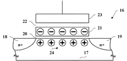
図2及び図3は、フラッシュメモリ2に含まれている1つのメモリセル16の構造を概略的に示す断面図である。図2では、メモリセル16にデータが書き込まれていない。図3では、メモリセル16にデータが書き込まれている。
図2及び図3に示されているように、メモリセル16は、P型半導体基板17と、N型ソース拡散領域18と、N型ドレイン拡散領域19と、トンネル酸化膜20と、フローティングゲート電極21と、絶縁膜22と、コントロールゲート電極23とを含んでいる。
2 and 3 are cross-sectional views schematically showing the structure of one
As shown in FIGS. 2 and 3, the
N型ソース拡散領域18及びN型ドレイン拡散領域19はともに、P型半導体基板17上に形成されている。トンネル酸化膜20は、N型ソース拡散領域18とN型ドレイン拡散領域19との間において、P型半導体基板17を覆っている。フローティングゲート電極21は、トンネル酸化膜20上に形成されている。絶縁膜22は、フローティングゲート電極21上に形成されている。コントロールゲート電極23は、絶縁膜22上に形成されている。フラッシュメモリ2では、複数のメモリセル16が直列に接続されている。1つのメモリセル16は、1ビットのデータを格納する。
Both the N-type
図2に示されているように、フローティングゲート電極21に電子が蓄積されていないとき、メモリセル16は、消去状態にある。他方、フローティングゲート電極21に電子が蓄積されているとき、メモリセル16は、書込状態にある。消去状態のメモリセル16は、論理値“1”を示すデータを格納している。書込状態のメモリセル16は、論理値“0”を示すデータを格納している。
As shown in FIG. 2, when no electrons are stored in the floating
メモリセル16に格納されたデータを読み出すために予め定められた読出電圧が、消去状態となっているメモリセル16のコントロールゲート電極23に印加されていないときには、N型ソース拡散領域18とN型ドレイン拡散領域19との間のP型半導体基板17の表面に、チャネルが形成されない。従って、N型ソース拡散領域18とN型ドレイン拡散領域19は、互いに電気的に絶縁される。
When a predetermined read voltage for reading data stored in
これに対して、消去状態となっているメモリセル16のコントロールゲート電極23に読出電圧が印加されているときには、N型ソース拡散領域18とN型ドレイン拡散領域19との間のP型半導体基板17の表面に、チャネル(図示せず)が形成される。N型ソース拡散領域18とN型ドレイン拡散領域19は、そのチャネルによって電気的に接続される。
In contrast, when a read voltage is applied to the
上述のように、消去状態となっているメモリセル16のコントロールゲート電極23に読出電圧が印加されていないときには、N型ソース拡散領域18とN型ドレイン拡散領域19が電気的に絶縁される。消去状態となっているメモリセル16のコントロールゲート電極23に読出電圧が印加されているときには、N型ソース拡散領域18とN型ドレイン拡散領域19が電気的に接続される。
As described above, when the read voltage is not applied to the
図3に示されているように、フローティングゲート電極21に電子が蓄積されているとき、メモリセル16は、書込状態にある。フローティングゲート電極21はトンネル酸化膜20と絶縁膜22に挟まれている。そのため、電子が一旦フローティングゲート電極21に注入されると、電位障壁により、きわめて長時間にわたり電子がフローティングゲート電極21内にとどまる。フローティングゲート電極21に電子を蓄積することにより書込状態となっているメモリセル16では、コントロールゲート電極23に読出電圧が印加されているか否かにかかわらず、チャネル24がN型ソース拡散領域18とN型ドレイン拡散領域19との間のP型半導体基板17の表面に形成される。従って、メモリセル16が書込状態となっているときには、コントロールゲート電極23に読出電圧が印加されているか否かにかかわらず、N型ソース拡散領域18とN型ドレイン拡散領域19が電気的に接続される。
As shown in FIG. 3, when electrons are accumulated in the floating
メモリセル16が消去状態であるか書込状態であるかを特定するためのデータ読出動作を、以下に説明する。フラッシュメモリ2では、複数のメモリセル16が直列に接続されている。その複数のメモリセル16のうちの1つが、格納データの読み出しのためにコントローラ3によって選択される。所定の低レベル電圧が、その選択された1つのメモリセル16に取り付けられたコントロールゲート電極23に印加される。低レベル電圧よりも高い所定の高レベル電圧(読出電圧)が、複数のメモリセル16のうちの他のものに取り付けられたコントロールゲート電極23に印加される。
A data read operation for specifying whether
この状況で、一連のメモリセル16が導通しているか否かを、所定の検出器により検出する。検出器が導通を検出したとき、選択されたメモリセル16は、書込状態である。検出器が不導通を検出したとき、選択されたメモリセル16は、消去状態である。上記のように、フラッシュメモリ2は、直列に接続された一連のメモリセル16のうちの任意の1つから論理値“0”又は“1”を示す格納データを読み出すように、設計されている。
In this situation, it is detected by a predetermined detector whether or not a series of
メモリセル16の状態を消去状態と書込状態との間で変更するときには、メモリセル16のデータ読出動作にて使用される電圧よりも大きい消去電圧又は書込電圧が使用される。消去状態となっているメモリセル16を書込状態に変更するときには、コントロールゲート電極23の電位がフローティングゲート電極21の電位よりも高くなるように、書込電圧がコントロールゲート電極23に印加される。この書込電圧によって、P型半導体基板17とフローティングゲート電極21の間に、トンネル酸化膜20を介してFN(ファウラーノルトハイム;Fowler-Nordhaim)トンネル電流が流れる。この結果、電子がフローティングゲート電極21に注入される。
When the state of the
他方、書込状態となっているメモリセル16を消去状態に変更するときには、コントロールゲート電極23の電位がフローティングゲート電極21の電位よりも低くなるように、消去電圧がコントロールゲート電極23に印加される。この消去電圧によって、フローティングゲート電極21に蓄積されている電子がトンネル酸化膜20を介してP型半導体基板17に排出される。
On the other hand, when the
以下に、フラッシュメモリ2にデータを格納するための構造を説明する。図4は、フラッシュメモリ2のアドレス空間を概略的に示している。図4に示された構造において、フラッシュメモリ2のアドレス空間は、“ページ”と“ブロック”に基づいて分割されている。ページは、フラッシュメモリ2にて行われるデータ読出動作及びデータ書込動作における処理単位である。ブロックは、フラッシュメモリ2にて行われるデータ消去動作における処理単位である。
The structure for storing data in the
1つのページは、512バイトのデータ領域25と、16バイトの冗長領域26とを含んでいる。データ領域25は、ホストコンピュータ4から供給されるユーザデータを格納する。冗長領域26は、ECCブロック11によって生成されたエラーコレクションコード(ECC)といった付加情報を格納する。エラーコレクションコードは、付加情報の1つであり、対応するデータ領域25に格納されたデータに含まれる誤りを訂正するために使用される。データ領域25に格納されたデータに含まれる誤りの数が予め定められた閾値以下であるときには、その誤りは、エラーコレクションコードによって訂正されることができる。このとき、データ領域25から読み出されたデータは、エラーコレクションコードによって正しいデータに修正される。
One page includes a
冗長領域26は、エラーコレクションコードの他に、“対応論理ブロックアドレス”を格納する。1つのブロックに含まれている少なくとも1つのデータ領域25に有効なデータが格納されているとき、対応論理ブロックアドレスは、そのブロックが対応付けられている論理ブロックのアドレスを示す。論理ブロックアドレスは、ホストコンピュータ4から与えられるホストアドレスに基づいて決定されるブロックのアドレスである。他方、フラッシュメモリ2内における実際のブロックのアドレスは、物理ブロックアドレスと称される。
The
1つのブロックに含まれている全てのデータ領域25に有効なデータが格納されていないときには、そのブロックに含まれている冗長領域26に、対応論理ブロックアドレスが格納されていない。従って、冗長領域26に対応論理ブロックアドレスが格納されているか否かを判定することにより、その冗長領域26が含まれているブロックにてデータが消去されたか否かを判定することができる。冗長領域26に対応論理ブロックアドレスが格納されていないとき、その冗長領域26が含まれているブロックは、データが消去された状態にある。
When valid data is not stored in all the
1つのブロックは、32個のページを含んでいる。フラッシュメモリ2では、データの上書きができない。そのため、1つのページに格納されたデータのみを書き換えるときであっても、そのページが含まれたブロック内の全ページに格納されたデータが、書き換えられなければならない。1つのブロック内の全ページから読み出されたデータの少なくとも一部が変更された後、そのデータは、消去されているブロックの1つに、ブロック単位で書き込まれなければならない。
One block includes 32 pages. In the
上記のようにデータを書き換えるにあたっては、書き換えられたデータは、以前に格納されていたブロックとは異なるブロックに書き込まれる。そのため、論理ブロックアドレスと物理ブロックアドレスの間の対応関係は、フラッシュメモリ2にてデータが書き換えられる毎に、動的に変化する。論理ブロックアドレスと物理ブロックアドレスの間の対応関係は、アドレス変換テーブルに記載される。アドレス変換テーブルは、図1に示されているワークエリア8に格納される。アドレス変換テーブルでは、フラッシュメモリ2にてデータが書き換えられる毎に、書き換えられたブロックに対応する格納情報が更新される。
In rewriting data as described above, the rewritten data is written in a block different from the previously stored block. Therefore, the correspondence between the logical block address and the physical block address dynamically changes every time data is rewritten in the
図1において、コントローラ3は、ホストインタフェース制御ブロック5と、マイクロプロセッサ6と、ホストインタフェースブロック7と、ワークエリア8と、バッファ9と、フラッシュメモリインタフェースブロック10と、ECCブロック11と、フラッシュシーケンサブロック12とを有している。例えば、コントローラ3は、1つの半導体チップ上に集積される。
In FIG. 1, the
以下に、コントローラ3の各部位の機能を説明する。ホストインタフェース制御ブロック5は、ホストインタフェースブロック7の動作を制御するための第1の制御ブロックである。マイクロプロセッサ6は、コントローラ3全体の動作を制御するための機能ブロックである。
Below, the function of each part of the
ホストインタフェースブロック7は、マイクロプロセッサ6による制御のもと、データ、アドレス及びその他の指示等を示す情報を、ホストコンピュータ4との間で交換するための機能ブロックである。フラッシュメモリシステム1がホストコンピュータ4に装着されたとき、フラッシュメモリシステム1とホストコンピュータ4とは、外部バス13を介して相互に接続される。ホストコンピュータ4からフラッシュメモリシステム1に供給される情報は、ホストインタフェースブロック7を通してコントローラ3の内部に取り込まれる。フラッシュメモリシステム1からホストコンピュータ4に供給される情報は、ホストインタフェースブロック7を通してホストコンピュータ4へ出力される。
The host interface block 7 is a functional block for exchanging information indicating data, addresses and other instructions with the host computer 4 under the control of the
ワークエリア8は、フラッシュメモリ2の制御に使用されるデータを一時的に格納するためのメモリモジュールである。例えば、ワークエリア8は、複数のSRAM(Static Random Access Memory)セルを含んでいる。
バッファ9は、フラッシュメモリ2から読み出されたデータ及びフラッシュメモリ2に書き込まれるべきデータを、保持するための機能ブロックである。フラッシュメモリ2から読み出されたデータは、ホストコンピュータ4に出力されるまで、バッファ9に保持される。フラッシュメモリ2に書き込まれるべきデータは、フラッシュメモリ2のデータ書込動作の準備ができるまで、バッファ9に保持される。
The work area 8 is a memory module for temporarily storing data used for controlling the
The
フラッシュメモリインタフェースブロック10は、内部バス14を介して、データ、アドレス、ステータス及び内部コマンド等を示す情報を、フラッシュメモリ2との間で交換するための機能ブロックである。内部コマンドは、コントローラ3からフラッシュメモリ2に与えられるコマンドである。
ECCブロック11は、フラッシュメモリ2への書込データに付加されるエラーコレクションコードを生成するための機能ブロックである。加えて、ECCブロック11は、フラッシュメモリ2から読み出されたデータに含まれるエラーコレクションコードに基づいて、読出データに含まれる誤りの検出及び訂正を行う。
The flash
The
フラッシュシーケンサブロック12は、内部コマンドに基づいて、フラッシュメモリ2の動作を制御するための第2の制御ブロックである。フラッシュシーケンサブロック12は、複数のレジスタ(図示せず)を有している。フラッシュシーケンサブロック12は、マイクロプロセッサ6による制御のもと、内部コマンドが実行されるときに使用される情報を、複数のレジスタに設定する。複数のレジスタに情報を設定した後、フラッシュシーケンサブロック12は、各レジスタに設定された情報に基づいて、内部コマンドに従った動作を行う。
The flash sequencer block 12 is a second control block for controlling the operation of the
以下に、フラッシュメモリ2からバッファ9にデータを読み出すための処理、及び、バッファ9からフラッシュメモリ2にデータを書き込むための処理について、説明する。
図5は、フラッシュメモリ2のメモリ空間31におけるブロック及びページの割当例を概略的に示している。図5に示されているように、メモリ空間31は、各々がデータ消去動作における一括処理単位である複数のブロック31a(B0000〜B1023)に分割されている。各ブロック31aは、各々がデータ読出動作及びデータ書込動作における一括処理単位である複数のページ31b(P00〜P31)に分割されている。各ページ31bは、各々が1バイトである512個のデータ領域(A000〜A511)に分割されている。
Hereinafter, a process for reading data from the
FIG. 5 schematically shows an example of block and page allocation in the
1024個のブロック31a(B0000〜B1023)は、1つのゾーンとして管理される。フラッシュメモリ2が複数のメモリ空間31を含んでいるとき、各メモリ空間31に対応した各ゾーンには、少なくとも1つの消去済ブロックが、データを書込可能とするために確保される。以下では、データを書込可能に設定された消去済ブロックは、書込候補ブロックと称される。データ書込動作では、書込候補ブロックの1つに、データが書き込まれる。
The 1024
図6は、フラッシュメモリ2のメモリ空間31と、バッファ9のバッファ空間32との間でのデータ交換動作を、概略的に示している。図6に示されているバッファ空間32は、各々が1バイトである512個のデータ領域(BF000〜BF511)に分割されている。バッファ空間32は、1バイト単位又は1ワード(2バイト又はより多くのバイト)単位で、フラッシュメモリ2との間でデータを交換する。
FIG. 6 schematically shows the data exchange operation between the
図6に示されているポインタレジスタ33及びジョブレジスタ34は、ホストコンピュータ4からの指示を格納する。フラッシュメモリ2からバッファ9にデータを読み出すための処理、及び、バッファ9からフラッシュメモリ2にデータを書き込む処理は、ポインタレジスタ33及びジョブレジスタ34に格納されている指示に従って、フラッシュシーケンサブロック12によって制御される。ポインタレジスタ33は、ページアドレスを設定するためのレジスタである。ジョブレジスタ34は、データ読出動作、データ書込動作等を示す動作指示を設定するためのレジスタである。
The
第1の例として、ジョブレジスタ34に設定された動作指示がデータ読出動作を示すとともに、ページアドレスがポインタレジスタ33に設定されたとき、フラッシュシーケンサブロック12が有する複数のレジスタ(図示せず)には、次のような情報が設定される。第1に、内部読出コマンドは、フラッシュシーケンサブロック12内の予め定められた第1レジスタ(図示せず)に、内部コマンドとして格納される。第2に、ポインタレジスタ33に設定されているページアドレスにおけるブロックアドレス部分(論理ブロックアドレス)は、フラッシュメモリ2内の対応するブロックアドレス(物理ブロックアドレス)に変換される。変換されたページアドレスは、フラッシュシーケンサブロック12内の予め定められた第2レジスタ(図示せず)に格納される。
As a first example, when the operation instruction set in the job register 34 indicates a data read operation and the page address is set in the
上記のようなデータ読出動作のために設定された情報に基づいて、フラッシュシーケンサブロック12は、内部コマンドに従ってフラッシュメモリインタフェースブロック10を制御する。フラッシュメモリインタフェースブロック10は、内部バス14を介してフラッシュメモリ2に、内部コマンドを示す情報を供給する。フラッシュメモリインタフェースブロック10から出力された情報に応答して、フラッシュメモリ2では、フラッシュシーケンサブロック12の第2レジスタに設定されたページアドレスに対応するデータ領域(A000〜A511)から、格納データが1バイト単位で順次に読み出される。フラッシュメモリ2から読み出されたデータは、バッファ空間32のデータ領域(BF000〜BF511)に順次格納される。例えば、フラッシュシーケンサブロック12は、フラッシュメモリ2から受けたデータを、バッファ空間32の開始アドレスから終了アドレスへと向かう順番で、バッファ空間32のデータ領域(BF000〜BF511)に順次格納するように、フラッシュメモリインタフェースブロック10を制御する。
Based on the information set for the data read operation as described above, the flash sequencer block 12 controls the flash
第2の例として、ジョブレジスタ34に設定された動作指示がデータ書込動作を示すとともに、ページアドレスがポインタレジスタ33に設定されたとき、フラッシュシーケンサブロック12が有する複数のレジスタ(図示せず)には、次のような情報が設定される。第1に、内部書込コマンドは、フラッシュシーケンサブロック12内の第1レジスタ(図示せず)に、内部コマンドとして格納される。第2に、ポインタレジスタ33に設定されているページアドレスの下位5ビットであるページ番号部分と、書込候補ブロックのブロックアドレス(物理ブロックアドレス)とに基づいて、ページアドレスが生成される。生成されたページアドレスは、フラッシュシーケンサブロック12内の第2レジスタ(図示せず)に格納される。
As a second example, when the operation instruction set in the job register 34 indicates a data write operation and the page address is set in the
上記のようなデータ書込動作のために設定された情報に基づいて、フラッシュシーケンサブロック12は、内部コマンドに従ってフラッシュメモリインタフェースブロック10を制御する。フラッシュメモリインタフェースブロック10は、内部バス14を介してフラッシュメモリ2に、内部コマンドを示す情報を供給する。同時に、フラッシュメモリインタフェースブロック10は、バッファ空間32のデータ領域(BF000〜BF511)に格納されているデータを読み出す。バッファ空間32から読み出されたデータは、1バイト単位で順次にフラッシュメモリ2へと供給される。例えば、フラッシュシーケンサブロック12は、バッファ空間32の開始アドレスから終了アドレスへと向かう順番で、フラッシュメモリ2に転送するためのデータをバッファ空間32から読み出すように、フラッシュメモリインタフェースブロック10を制御する。フラッシュメモリインタフェースブロック10から出力された情報に応答して、フラッシュメモリ2では、フラッシュシーケンサブロック12の第2レジスタに設定されたページアドレスに対応するデータ領域(A000〜A511)に、コントローラ3から供給されたデータが順次に書き込まれる。
Based on the information set for the data write operation as described above, the flash sequencer block 12 controls the flash
コントローラ3がフラッシュメモリ2における一連のページとデータを交換するときには、“開始ページアドレス”及び“終了ページアドレス”がポインタレジスタ33に設定されてもよい。フラッシュシーケンサブロック12内の第2レジスタに設定されるページアドレスの下位5ビットであるページ番号部分は、“開始ページアドレス”から“終了ページアドレス”まで、1ずつカウントアップされる。別の設定として、“開始ページアドレス”及び“ページ数”がポインタレジスタ33に設定されてもよい。フラッシュシーケンサブロック12内の第2レジスタに設定されるページ番号部分は、“開始ページアドレス”から1ずつカウントアップされる。カウントアップ動作は、“ページ数”に対応する回数まで実行される。
When the
以下に、フラッシュメモリ2に格納されているデータをホストコンピュータ4へと読み出すための処理、及び、ホストコンピュータ4からフラッシュメモリ2にデータを書き込むための処理について、説明する。
Hereinafter, processing for reading data stored in the
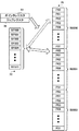
図7は、ホストコンピュータ4のメモリアドレス空間38と、バッファ9のバッファ空間32との間でのデータ交換動作を、概略的に示している。図7には、ポインタレジスタ33及びジョブレジスタ34も示されている。
バッファ9のバッファ空間32は、ホストコンピュータ4のメモリアドレス空間38において、512バイトを有するメモリ領域(M10000〜M10511)に割り付けられている。ホストコンピュータ4のメモリアドレス空間38には、ポインタレジスタ33及びジョブレジスタ34にアクセスするためのアドレスが含まれている。メモリアドレス空間38にてポインタレジスタ33及びジョブレジスタ34に割り当てられるアドレスは、ポインタレジスタ33及びジョブレジスタ34のデータ容量に応じて、適宜設定されていればよい。ホストコンピュータ4にてポインタレジスタ33及びジョブレジスタ34に割り当てられるアドレスは、ホストコンピュータ4のI/Oアドレス空間に含まれていてもよい。
FIG. 7 schematically shows the data exchange operation between the
The
図8は、ホストコンピュータ4のメモリ領域35と、フラッシュメモリ2のメモリ空間31との間でのデータ交換動作を、概略的に示している。フラッシュメモリ2から読み出されたデータ及びフラッシュメモリ2に書き込まれるべきデータは、バッファ9のバッファ空間32を介して、メモリ領域35とメモリ空間31との間で交換される。バッファ空間32は、ホストコンピュータ4のメモリアドレス空間38において、512バイトを有するメモリ領域35に割り付けられている。フラッシュメモリ2のメモリ空間31に格納されているデータを読み出すため、及び、フラッシュメモリ2のメモリ空間31にデータを書き込むために、ホストコンピュータ4は、バッファ空間32に割り付けられているメモリ領域35にアクセスする。コントローラ3は、ポインタレジスタ33及びジョブレジスタ34における設定情報に基づいて、バッファ空間32とメモリ空間31の全データ領域との間で、データを交換できるようにする。
FIG. 8 schematically shows the data exchange operation between the
コントローラ3がバッファ空間32とフラッシュメモリ2のメモリ空間31との間でデータを交換するとき、コントローラ3に含まれるアドレスカウンタ36は、1ページ分(512バイト)のデータが順次に交換されるように制御する。例えば、アドレスカウンタ36は、フラッシュシーケンサブロック12に含まれている。他方、ホストコンピュータ4とバッファ9との間でデータが交換されるときには、アドレスバッファ37を用いることにより、通常のスタティックRAMと同様に、512バイトを有するバッファ空間32における各データ領域が、所定のアドレスバスによって供給されるアドレス信号及び制御信号に基づいて、ランダムにアクセスされる。例えば、アドレスバッファ37は、ホストインタフェース制御ブロック5に含まれている。
When the
バッファ空間32のデータ容量は512(=29)バイトである。従って、バッファ空間32の各データ領域は、9ビットのアドレスによって特定されることができる。ホストコンピュータ4のメモリ領域35から供給されるアドレスデータの下位9ビットは、バッファ空間32における各データ領域のアドレスを示す。バッファ空間32における各データ領域のアドレスを示すデータは、アドレスバッファ37にセットされる。アドレスバッファ37にセットされたアドレスデータに基づいて、ホストインタフェース制御ブロック5は、ホストコンピュータ4がバッファ空間32の各データ領域にアクセスすることを可能にする。ホストコンピュータ4のメモリ領域35から供給されるアドレスデータのうちでアドレスバッファ37にセットされなかったデータは、バッファ空間32に保持されているデータがホストコンピュータ4からの要求に適合しているか否かを判定するために使用される。この判定処理は、例えば、マイクロプロセッサ6によって実行される。
The data capacity of the
ホストコンピュータ4がワード(16ビット)単位でバッファ空間32にアクセスするときには、ホストコンピュータ4のメモリ空間35から供給されるアドレスデータの下位8ビットがアドレスバッファ37にセットされてもよい。バッファ空間32の各データ領域は、8ビットのアドレスによって特定されることができる。このときにも、ホストコンピュータ4のメモリ領域35から供給されるアドレスデータのうちでアドレスバッファ37にセットされなかったデータに基づいて、コントローラ3は、バッファ空間32に保持されているデータがホストコンピュータ4からの要求に適合しているか否かを判定することができる。
When the host computer 4 accesses the
以下に、図9から図12に示されるタイミング図を参照することにより、ホストコンピュータ4のメモリ領域35によるバッファ空間32からのデータ読出動作と、バッファ空間32へのデータ書込動作について、説明する。
The data read operation from the
図9は、ホストコンピュータ4のメモリ領域35におけるデータ読出サイクルを示すタイミング図である。ホストコンピュータ4は、メモリ領域35を介して所定のアドレスバスにアドレス信号ADRを出力する。この出力に対応して、チップイネーブル信号CEN及びアウトプットイネーブル信号OENは低レベルになる。アドレス信号ADRが出力されている期間では、チップイネーブル信号CEN及びアウトプットイネーブル信号OENが低レベルに設定される。バッファ9では、アドレス信号ADRによって指定されたアドレスを有するバッファ空間32のデータ領域に格納されているデータが読み出される。読み出されたデータは、データ信号DATAとして、ホストインタフェースブロック7を介して、ホストコンピュータ4へと出力される。ホストインタフェース制御ブロック5は、ホストコンピュータ4へとデータ信号DATAを出力するために、ホストコンピュータ4から供給されたアドレス信号ADRによって指定されたアドレスを有するバッファ空間32のデータ領域から格納データを読み出すように、ホストインタフェースブロック7を制御する。図9において、アドレス信号ADRによってアドレスA0が指定されたことに応答して、データD0を示すデータ信号DATAが出力される。アドレス信号ADRによってアドレスA1が指定されたことに応答して、データD1を示すデータ信号DATAが出力される。
FIG. 9 is a timing chart showing a data read cycle in the
図10は、ホストコンピュータ4がバッファ9から連続的に格納データを読み出すための動作を示すタイミング図である。図10において、ホストコンピュータ4は、アドレスA’からアドレスA’+3を示すアドレス信号ADRを、連続してコントローラ3に出力する。アドレス信号ADRが連続して出力されている期間では、チップイネーブル信号CEN及びアウトプットイネーブル信号OENが低レベルに設定される。バッファ9では、アドレス信号ADRによって指定されたアドレスA’−A’+3を有するバッファ空間32のデータ領域に格納されているデータが順次に読み出される。読み出されたデータは、データ信号DATAとして、ホストコンピュータ4へと順次に出力される。
FIG. 10 is a timing chart showing an operation for the host computer 4 to continuously read stored data from the
図10において、アドレス信号ADRによってアドレスA’が指定されたことに応答して、データD0’を示すデータ信号DATAが出力される。アドレス信号ADRによってアドレスA’+1が指定されたことに応答して、データD1’を示すデータ信号DATAが出力される。アドレス信号ADRによってアドレスA’+2が指定されたことに応答して、データD2’を示すデータ信号DATAが出力される。アドレス信号ADRによってアドレスA’+3が指定されたことに応答して、データD3’を示すデータ信号DATAが出力される。 In FIG. 10, in response to the address A 'being designated by the address signal ADR, the data signal DATA indicating the data D0' is output. In response to the address A ′ + 1 being designated by the address signal ADR, the data signal DATA indicating the data D1 ′ is output. In response to the address A '+ 2 being designated by the address signal ADR, the data signal DATA indicating the data D2' is output. In response to the address A '+ 3 being designated by the address signal ADR, the data signal DATA indicating the data D3' is output.
図11は、ホストコンピュータ4のメモリ領域35及びバッファ9のバッファ空間32におけるデータ書込サイクルを示すタイミング図である。ホストコンピュータ4は、メモリ領域35を介して、所定のアドレスバスにアドレス信号ADRを出力し、所定のデータバスにデータ信号DATAを出力する。このアドレス信号ADR及びデータ信号DATAの出力に対応して、チップイネーブル信号CENは低レベルに設定される。アドレス信号ADR及びデータ信号DATAが出力されている期間において、チップイネーブル信号CENが低レベルになる。アドレス信号ADR、データ信号DATA及び低レベルのチップイネーブル信号CENが出力されている期間において、ライトイネーブル信号WENが低レベルから高レベルに変化する。
FIG. 11 is a timing chart showing a data write cycle in the
ライトイネーブル信号WENの立ち上がりエッジに応答して、データ信号DATAが、アドレス信号ADRで指定されたアドレスを有するバッファ空間32のデータ領域に取り込まれる。ホストインタフェース制御ブロック5は、ホストコンピュータ4から供給されたアドレス信号ADRによって指定されたアドレスを有するメモリ空間31のデータ領域に、ホストコンピュータ4から供給されたデータ信号DATAによって示されるデータを書き込むように、ホストインタフェースブロック7を制御する。図11では、データ信号DATAによって示されるデータD0が、アドレス信号ADRによって指定されたアドレスA0を有するデータ領域に格納される。データ信号DATAによって示されるデータD1は、アドレス信号ADRによって指定されたアドレスA1を有するデータ領域に格納される。
In response to the rising edge of the write enable signal WEN, the data signal DATA is taken into the data area of the
図12は、ホストコンピュータ4がバッファ9に連続的にデータを書き込むための動作を示すタイミング図である。図12において、ホストコンピュータ4は、アドレスA’からアドレスA’+3を示すアドレス信号ADRを、連続してコントローラ3に出力する。アドレスA’を指定するアドレス信号が出力されるときには、データD0’を示すデータ信号DATAが出力される。アドレスA’+1を指定するアドレス信号ADRが出力されるときには、データD1’を示すデータ信号DATAが出力される。アドレスA’+2を指定するアドレス信号ADRが出力されるときには、データD2’を示すデータ信号DATAが出力される。アドレスA’+3を指定するアドレス信号ADRが出力されるときには、データD3’を示すデータ信号DATAが出力される。アドレス信号ADRが連続して出力されている期間において、チップイネーブル信号CENが低レベルになる。アドレス信号ADR、データ信号DATA及び低レベルのチップイネーブル信号CENが出力されている期間において、ホストコンピュータ4は、ライトイネーブル信号WENを低レベルから高レベルにさせる。ライトイネーブル信号WENの立ち上がりエッジに応答して、データ信号DATAが、アドレス信号ADRで指定されたアドレスを有するバッファ空間32のデータ領域に取り込まれる。
FIG. 12 is a timing chart showing an operation for the host computer 4 to continuously write data to the
図12では、データ信号DATAによって示されるデータD0’が、アドレス信号ADRによって指定されたアドレスA’を有するデータ領域に格納される。データ信号DATAによって示されるデータD1’は、アドレス信号ADRによって指定されたアドレスA’+1を有するデータ領域に格納される。データ信号DATAによって示されるデータD2’は、アドレス信号ADRによって指定されたアドレスA’+2を有するデータ領域に格納される。データ信号DATAによって示されるデータD3’は、アドレス信号ADRによって指定されたアドレスA’+3を有するデータ領域に格納される。 In FIG. 12, the data D0 'indicated by the data signal DATA is stored in the data area having the address A' designated by the address signal ADR. Data D1 'indicated by the data signal DATA is stored in a data area having an address A' + 1 specified by the address signal ADR. Data D2 'indicated by the data signal DATA is stored in a data area having an address A' + 2 designated by the address signal ADR. Data D3 'indicated by the data signal DATA is stored in a data area having an address A' + 3 specified by the address signal ADR.
フラッシュメモリ2のメモリ空間31においてポインタレジスタ33によって指定されたページアドレスを有するページ31b(P00〜P31)と、バッファ9のバッファ空間32との間では、バッファ空間32の先頭から末尾まで、順次にデータが交換される。言い換えると、フラッシュメモリ2とコントローラ3との間でのデータ交換は、フラッシュメモリ2におけるページを単位として行われる。ホストコンピュータ4は、メモリ領域35にアクセスすることにより、バッファ9のバッファ空間32に含まれる任意のデータ領域との間でランダムにデータを交換することができる。バッファ9のバッファ空間32は、フラッシュメモリ2のメモリ空間31における1つのページと同様に、512バイトの記憶容量を有している。従って、コントローラ3は、簡単な構成で、ホストコンピュータ4にフラッシュメモリ2への柔軟なアクセスを提供することができる。コントローラ3によって提供されるフラッシュメモリ2へのメモリアクセスは、通常のスタティックRAMへのアクセスと類似している。
Between the
本発明は、様々な変形及び応用が可能である。例えば、コントローラ3は、フラッシュメモリシステム1とは独立して、フラッシュメモリ2とホストコンピュータ4との間でのデータ交換を制御してもよい。コントローラ3は、ホストコンピュータ4に内蔵されていてもよい。ポインタレジスタ33及びジョブレジスタ34は、SRAMやDRAM(Dynamic RAM)などといった、ホストコンピュータ4からのランダムアクセスが可能な任意のメモリに置き換えられてもよい。
The present invention can be variously modified and applied. For example, the
1 フラッシュメモリシステム
2、31 フラッシュメモリ
3 コントローラ
4、35 ホストコンピュータ
5 ホストインタフェース制御ブロック
6 マイクロプロセッサ
7 ホストインタフェースブロック
8 ワークエリア
9,32 バッファ
10 フラッシュメモリインタフェースブロック
11 ECCブロック
12 フラッシュシーケンサブロック
13 外部バス
14 内部バス
16 メモリセル
17 P型半導体基板
18 N型ソース拡散領域
19 N型ドレイン拡散領域
20 トンネル酸化膜
21 フローティングゲート電極
22 絶縁膜
23 コントロールゲート電極
24 チャネル
25 データ領域
26 冗長領域
33 ポインタレジスタ
34 ジョブレジスタ
36 アドレスカウンタ
37 アドレスバッファ
38 メモリアドレス空間
1
Claims (3)
前記フラッシュメモリに書き込むデータ又は前記フラッシュメモリから読み出されたデータを保持する手段であって、ホストシステムのメモリアドレス空間に割り当てられているバッファと、
ホストシステム側から、該ホストシステムのメモリアドレス空間におけるアクセス単位で、前記バッファにランダムアクセスできるように制御し、さらに、前記ホストシステム側から与えられる複数ビットのアドレスを所定の上位側ビットと下位側ビットに分離し、該上位側ビットに基づいて前記バッファに保持されているデータがアクセス対象のデータに該当するか否かを判別し、該下位側ビットに基づいて前記バッファ内のアクセス領域を識別するホストインタフェース制御手段と、
前記ホストシステム側から与えられるアクセス対象の論理ページを特定するための論理ページアドレスが保持されるアドレス保持手段と、
複数の前記論理ページを含む論理ブロックに付けられたアドレスである論理ブロックアドレスと、前記物理ブロックに付けられたアドレスである物理ブロックアドレスとの対応関係を管理するアドレス管理手段と、
前記アドレス保持手段に保持されている前記論理ページアドレスの前記論理ブロックアドレスに対応する所定の上位側ビット部分を、該論理ブロックアドレスと対応する前記物理ブロックアドレスに置き換えた物理ページアドレスを生成するアドレス生成手段と、
前記アドレス生成手段によって生成された前記物理ページアドレスに対応する前記物理ページにデータを書き込むための前記バッファから前記フラッシュメモリへの512バイト単位のデータ転送と、前記アドレス生成手段によって生成された前記物理ページアドレスに対応する前記物理ページからデータを読み出すための前記フラッシュメモリから前記バッファへの512バイト単位のデータ転送とを制御するフラッシュメモリインタフェース制御手段と、
を備えることを特徴とするフラッシュメモリコントローラ。 A memory controller for controlling access to a flash memory in which stored data is erased in units of physical blocks including a plurality of physical pages,
Means for holding data to be written to the flash memory or data read from the flash memory, and a buffer assigned to a memory address space of a host system;
From the host system side, control is performed so that the buffer can be randomly accessed in an access unit in the memory address space of the host system. Further, a plurality of bits given from the host system side are assigned a predetermined upper bit and lower side. It is divided into bits, and it is determined whether the data held in the buffer corresponds to the data to be accessed based on the upper bit, and the access area in the buffer is identified based on the lower bit and host Inn tough Esu control means for,
Address holding means for holding a logical page address for specifying a logical page to be accessed given from the host system side;
Address management means for managing a correspondence relationship between a logical block address that is an address attached to a logical block including a plurality of the logical pages and a physical block address that is an address attached to the physical block;
An address for generating a physical page address in which a predetermined upper bit portion corresponding to the logical block address of the logical page address held in the address holding means is replaced with the physical block address corresponding to the logical block address Generating means;
512-byte data transfer from the buffer to the flash memory for writing data to the physical page corresponding to the physical page address generated by the address generating means, and the physical generated by the address generating means Flash memory interface control means for controlling data transfer in units of 512 bytes from the flash memory to the buffer for reading data from the physical page corresponding to a page address;
A flash memory controller comprising:
アクセス対象の論理ページを特定するための論理ページアドレスが保持されるアドレス保持手段に、ホストシステム側から与えられる複数ビットの前記論理ページアドレスを保持する論理ページアドレス保持ステップと、
複数の前記論理ページを含む論理ブロックに付けられたアドレスである論理ブロックアドレスと、前記物理ブロックに付けられたアドレスである物理ブロックアドレスとの対応関係を管理するアドレス管理ステップと、
前記アドレス保持手段に保持されている前記論理ページアドレスの前記論理ブロックアドレスに対応する所定の上位側ビット部分を、該論理ブロックアドレスと対応する前記物理ブロックアドレスに置き換えた物理ページアドレスを生成するアドレス生成ステップと、
512バイトの転送単位で、前記アドレス生成ステップで生成された前記物理ページアドレスに対応する前記物理ページに書き込まれるデータ又は前記アドレス生成ステップで生成された前記物理ページアドレスに対応する前記物理ページから読み出されたデータを保持するバッファと前記フラッシュメモリとの間でのデータ転送を制御するデータ転送ステップと、
ホストシステム側から与えられる複数ビットのアドレスを所定の上位側ビットと下位側ビットに分離し、前記上位側ビットに基づいて、前記バッファに保持されているデータがアクセス対象のデータに該当するか否かを判別し、該下位側ビットに基づいて前記バッファ内のアクセス領域を識別する識別ステップと、
前記ホストシステム側から、該ホストシステムのメモリアドレス空間におけるアクセス単位で、前記バッファにランダムアクセスできるように制御するアクセス制御ステップとを有し、
前記バッファは、前記ホストシステムのメモリアドレス空間に割り当てられていることを特徴とするフラッシュメモリの制御方法。 A flash memory control method for controlling access to a flash memory in which stored data is erased in units of physical blocks including a plurality of physical pages ,
A logical page address holding step for holding a plurality of bits of the logical page address given from the host system side in an address holding means for holding a logical page address for specifying a logical page to be accessed ;
An address management step for managing a correspondence relationship between a logical block address that is an address attached to a logical block including a plurality of the logical pages and a physical block address that is an address attached to the physical block;
An address for generating a physical page address in which a predetermined upper bit portion corresponding to the logical block address of the logical page address held in the address holding means is replaced with the physical block address corresponding to the logical block address Generation step;
Data is written to the physical page corresponding to the physical page address generated in the address generation step or read from the physical page corresponding to the physical page address generated in the address generation step in a 512-byte transfer unit. A data transfer step for controlling data transfer between the buffer for holding the issued data and the flash memory ;
A multi-bit address given from the host system side is separated into predetermined higher-order bits and lower-order bits, and whether or not the data held in the buffer corresponds to the data to be accessed based on the higher-order bits An identification step of identifying the access area in the buffer based on the lower-order bits;
Wherein the host system side, the access unit in the memory address space of the host system, and a access control step of controlling to allow random access to the buffer,
A method of controlling a flash memory, wherein the buffer is allocated to a memory address space of the host system.
Priority Applications (1)
| Application Number | Priority Date | Filing Date | Title |
|---|---|---|---|
| JP2004172262A JP4068594B2 (en) | 2003-06-10 | 2004-06-10 | Flash memory controller, flash memory system, and flash memory control method |
Applications Claiming Priority (2)
| Application Number | Priority Date | Filing Date | Title |
|---|---|---|---|
| JP2003165656 | 2003-06-10 | ||
| JP2004172262A JP4068594B2 (en) | 2003-06-10 | 2004-06-10 | Flash memory controller, flash memory system, and flash memory control method |
Publications (3)
| Publication Number | Publication Date |
|---|---|
| JP2005025733A JP2005025733A (en) | 2005-01-27 |
| JP2005025733A5 JP2005025733A5 (en) | 2007-03-15 |
| JP4068594B2 true JP4068594B2 (en) | 2008-03-26 |
Family
ID=34196947
Family Applications (1)
| Application Number | Title | Priority Date | Filing Date |
|---|---|---|---|
| JP2004172262A Expired - Fee Related JP4068594B2 (en) | 2003-06-10 | 2004-06-10 | Flash memory controller, flash memory system, and flash memory control method |
Country Status (1)
| Country | Link |
|---|---|
| JP (1) | JP4068594B2 (en) |
Families Citing this family (3)
| Publication number | Priority date | Publication date | Assignee | Title |
|---|---|---|---|---|
| JP4670370B2 (en) * | 2005-01-28 | 2011-04-13 | Tdk株式会社 | Memory controller and flash memory system |
| KR100706246B1 (en) * | 2005-05-24 | 2007-04-11 | 삼성전자주식회사 | Memory card capable of improving read performance |
| JP2010277352A (en) * | 2009-05-28 | 2010-12-09 | Toshiba Corp | Memory system |
-
2004
- 2004-06-10 JP JP2004172262A patent/JP4068594B2/en not_active Expired - Fee Related
Also Published As
| Publication number | Publication date |
|---|---|
| JP2005025733A (en) | 2005-01-27 |
Similar Documents
| Publication | Publication Date | Title |
|---|---|---|
| US9075740B2 (en) | Memory system | |
| US7006383B2 (en) | Nonvolatile semiconductor memory for management of a number of data writer/erase times | |
| US20030033567A1 (en) | Memory card and memory controller | |
| JPH06111589A (en) | Batched-erasure nonvolatile semiconductor memory device | |
| JP2008524705A (en) | Scratch pad block | |
| JP2006018373A (en) | Memory controller, flash memory system and control method for flash memory | |
| JP2012058770A (en) | Memory controller, flash memory system equipped with memory controller and control method of flash memory | |
| US7606993B2 (en) | Flash memory controller, memory control circuit, flash memory system, and method for controlling data exchange between host computer and flash memory | |
| JP4661191B2 (en) | Memory controller, flash memory system, and flash memory control method | |
| JP4068594B2 (en) | Flash memory controller, flash memory system, and flash memory control method | |
| JP2012068765A (en) | Memory controller, flash memory system with memory controller, and control method of flash memory | |
| JP4433792B2 (en) | MEMORY CONTROLLER, FLASH MEMORY SYSTEM PROVIDED WITH MEMORY CONTROLLER, AND FLASH MEMORY CONTROL METHOD | |
| JP2008123241A (en) | Memory controller, flash memory system equipped with memory controller, and method for controlling flash memory | |
| JP4582078B2 (en) | Memory controller, flash memory system, and flash memory control method | |
| JP4177292B2 (en) | MEMORY CONTROLLER, FLASH MEMORY SYSTEM, AND FLASH MEMORY CONTROL METHOD | |
| JP3934659B1 (en) | Memory controller and flash memory system | |
| JP2005292925A (en) | Memory controller, flash memory system, and control method for flash memory | |
| JP4177301B2 (en) | Memory controller, flash memory system, and flash memory control method | |
| JP4419525B2 (en) | MEMORY CONTROLLER, FLASH MEMORY SYSTEM PROVIDED WITH MEMORY CONTROLLER, AND FLASH MEMORY CONTROL METHOD | |
| JP4332108B2 (en) | Memory controller, flash memory system, and flash memory control method | |
| JP2012037971A (en) | Memory controller, nonvolatile memory system provided with memory controller, and method for controlling nonvolatile memory | |
| JP4222879B2 (en) | MEMORY CONTROLLER, FLASH MEMORY SYSTEM PROVIDED WITH MEMORY CONTROLLER, AND FLASH MEMORY CONTROL METHOD | |
| JP2006048746A (en) | Memory card | |
| JP4251950B2 (en) | MEMORY CONTROLLER, FLASH MEMORY SYSTEM PROVIDED WITH MEMORY CONTROLLER, AND FLASH MEMORY CONTROL METHOD | |
| JP4561110B2 (en) | MEMORY CONTROLLER, FLASH MEMORY SYSTEM PROVIDED WITH MEMORY CONTROLLER, AND FLASH MEMORY CONTROL METHOD |
Legal Events
| Date | Code | Title | Description |
|---|---|---|---|
| A521 | Request for written amendment filed |
Free format text: JAPANESE INTERMEDIATE CODE: A523 Effective date: 20070130 |
|
| A977 | Report on retrieval |
Free format text: JAPANESE INTERMEDIATE CODE: A971007 Effective date: 20070322 |
|
| A131 | Notification of reasons for refusal |
Free format text: JAPANESE INTERMEDIATE CODE: A131 Effective date: 20070327 |
|
| A521 | Request for written amendment filed |
Free format text: JAPANESE INTERMEDIATE CODE: A523 Effective date: 20070528 |
|
| A131 | Notification of reasons for refusal |
Free format text: JAPANESE INTERMEDIATE CODE: A131 Effective date: 20070807 |
|
| A521 | Request for written amendment filed |
Free format text: JAPANESE INTERMEDIATE CODE: A523 Effective date: 20071009 |
|
| A131 | Notification of reasons for refusal |
Free format text: JAPANESE INTERMEDIATE CODE: A131 Effective date: 20071030 |
|
| A521 | Request for written amendment filed |
Free format text: JAPANESE INTERMEDIATE CODE: A523 Effective date: 20071130 |
|
| TRDD | Decision of grant or rejection written | ||
| A01 | Written decision to grant a patent or to grant a registration (utility model) |
Free format text: JAPANESE INTERMEDIATE CODE: A01 Effective date: 20080108 |
|
| A61 | First payment of annual fees (during grant procedure) |
Free format text: JAPANESE INTERMEDIATE CODE: A61 Effective date: 20080110 |
|
| FPAY | Renewal fee payment (event date is renewal date of database) |
Free format text: PAYMENT UNTIL: 20110118 Year of fee payment: 3 |
|
| R150 | Certificate of patent or registration of utility model |
Free format text: JAPANESE INTERMEDIATE CODE: R150 Ref document number: 4068594 Country of ref document: JP Free format text: JAPANESE INTERMEDIATE CODE: R150 |
|
| FPAY | Renewal fee payment (event date is renewal date of database) |
Free format text: PAYMENT UNTIL: 20110118 Year of fee payment: 3 |
|
| FPAY | Renewal fee payment (event date is renewal date of database) |
Free format text: PAYMENT UNTIL: 20120118 Year of fee payment: 4 |
|
| FPAY | Renewal fee payment (event date is renewal date of database) |
Free format text: PAYMENT UNTIL: 20120118 Year of fee payment: 4 |
|
| FPAY | Renewal fee payment (event date is renewal date of database) |
Free format text: PAYMENT UNTIL: 20130118 Year of fee payment: 5 |
|
| FPAY | Renewal fee payment (event date is renewal date of database) |
Free format text: PAYMENT UNTIL: 20130118 Year of fee payment: 5 |
|
| FPAY | Renewal fee payment (event date is renewal date of database) |
Free format text: PAYMENT UNTIL: 20140118 Year of fee payment: 6 |
|
| LAPS | Cancellation because of no payment of annual fees |