JP4049112B2 - Electronic equipment - Google Patents
Electronic equipment Download PDFInfo
- Publication number
- JP4049112B2 JP4049112B2 JP2004064973A JP2004064973A JP4049112B2 JP 4049112 B2 JP4049112 B2 JP 4049112B2 JP 2004064973 A JP2004064973 A JP 2004064973A JP 2004064973 A JP2004064973 A JP 2004064973A JP 4049112 B2 JP4049112 B2 JP 4049112B2
- Authority
- JP
- Japan
- Prior art keywords
- sensor
- circuit
- power
- signal processing
- processing circuit
- Prior art date
- Legal status (The legal status is an assumption and is not a legal conclusion. Google has not performed a legal analysis and makes no representation as to the accuracy of the status listed.)
- Expired - Fee Related
Links
Images


Classifications
-
- H—ELECTRICITY
- H05—ELECTRIC TECHNIQUES NOT OTHERWISE PROVIDED FOR
- H05K—PRINTED CIRCUITS; CASINGS OR CONSTRUCTIONAL DETAILS OF ELECTRIC APPARATUS; MANUFACTURE OF ASSEMBLAGES OF ELECTRICAL COMPONENTS
- H05K1/00—Printed circuits
- H05K1/18—Printed circuits structurally associated with non-printed electric components
- H05K1/181—Printed circuits structurally associated with non-printed electric components associated with surface mounted components
-
- H—ELECTRICITY
- H05—ELECTRIC TECHNIQUES NOT OTHERWISE PROVIDED FOR
- H05K—PRINTED CIRCUITS; CASINGS OR CONSTRUCTIONAL DETAILS OF ELECTRIC APPARATUS; MANUFACTURE OF ASSEMBLAGES OF ELECTRICAL COMPONENTS
- H05K1/00—Printed circuits
- H05K1/02—Details
- H05K1/0213—Electrical arrangements not otherwise provided for
- H05K1/0216—Reduction of cross-talk, noise or electromagnetic interference
- H05K1/0218—Reduction of cross-talk, noise or electromagnetic interference by printed shielding conductors, ground planes or power plane
-
- H—ELECTRICITY
- H05—ELECTRIC TECHNIQUES NOT OTHERWISE PROVIDED FOR
- H05K—PRINTED CIRCUITS; CASINGS OR CONSTRUCTIONAL DETAILS OF ELECTRIC APPARATUS; MANUFACTURE OF ASSEMBLAGES OF ELECTRICAL COMPONENTS
- H05K1/00—Printed circuits
- H05K1/02—Details
- H05K1/0296—Conductive pattern lay-out details not covered by sub groups H05K1/02 - H05K1/0295
- H05K1/0298—Multilayer circuits
-
- H—ELECTRICITY
- H05—ELECTRIC TECHNIQUES NOT OTHERWISE PROVIDED FOR
- H05K—PRINTED CIRCUITS; CASINGS OR CONSTRUCTIONAL DETAILS OF ELECTRIC APPARATUS; MANUFACTURE OF ASSEMBLAGES OF ELECTRICAL COMPONENTS
- H05K2201/00—Indexing scheme relating to printed circuits covered by H05K1/00
- H05K2201/07—Electric details
- H05K2201/0707—Shielding
- H05K2201/0723—Shielding provided by an inner layer of PCB
-
- H—ELECTRICITY
- H05—ELECTRIC TECHNIQUES NOT OTHERWISE PROVIDED FOR
- H05K—PRINTED CIRCUITS; CASINGS OR CONSTRUCTIONAL DETAILS OF ELECTRIC APPARATUS; MANUFACTURE OF ASSEMBLAGES OF ELECTRICAL COMPONENTS
- H05K2201/00—Indexing scheme relating to printed circuits covered by H05K1/00
- H05K2201/10—Details of components or other objects attached to or integrated in a printed circuit board
- H05K2201/10007—Types of components
- H05K2201/10151—Sensor
-
- H—ELECTRICITY
- H05—ELECTRIC TECHNIQUES NOT OTHERWISE PROVIDED FOR
- H05K—PRINTED CIRCUITS; CASINGS OR CONSTRUCTIONAL DETAILS OF ELECTRIC APPARATUS; MANUFACTURE OF ASSEMBLAGES OF ELECTRICAL COMPONENTS
- H05K2201/00—Indexing scheme relating to printed circuits covered by H05K1/00
- H05K2201/10—Details of components or other objects attached to or integrated in a printed circuit board
- H05K2201/10613—Details of electrical connections of non-printed components, e.g. special leads
- H05K2201/10621—Components characterised by their electrical contacts
- H05K2201/10689—Leaded Integrated Circuit [IC] package, e.g. dual-in-line [DIL]
-
- H—ELECTRICITY
- H05—ELECTRIC TECHNIQUES NOT OTHERWISE PROVIDED FOR
- H05K—PRINTED CIRCUITS; CASINGS OR CONSTRUCTIONAL DETAILS OF ELECTRIC APPARATUS; MANUFACTURE OF ASSEMBLAGES OF ELECTRICAL COMPONENTS
- H05K2203/00—Indexing scheme relating to apparatus or processes for manufacturing printed circuits covered by H05K3/00
- H05K2203/15—Position of the PCB during processing
- H05K2203/1572—Processing both sides of a PCB by the same process; Providing a similar arrangement of components on both sides; Making interlayer connections from two sides
-
- Y—GENERAL TAGGING OF NEW TECHNOLOGICAL DEVELOPMENTS; GENERAL TAGGING OF CROSS-SECTIONAL TECHNOLOGIES SPANNING OVER SEVERAL SECTIONS OF THE IPC; TECHNICAL SUBJECTS COVERED BY FORMER USPC CROSS-REFERENCE ART COLLECTIONS [XRACs] AND DIGESTS
- Y02—TECHNOLOGIES OR APPLICATIONS FOR MITIGATION OR ADAPTATION AGAINST CLIMATE CHANGE
- Y02P—CLIMATE CHANGE MITIGATION TECHNOLOGIES IN THE PRODUCTION OR PROCESSING OF GOODS
- Y02P70/00—Climate change mitigation technologies in the production process for final industrial or consumer products
- Y02P70/50—Manufacturing or production processes characterised by the final manufactured product
Landscapes
- Engineering & Computer Science (AREA)
- Microelectronics & Electronic Packaging (AREA)
- Transceivers (AREA)
- Arrangements For Transmission Of Measured Signals (AREA)
- Air Conditioning Control Device (AREA)
- Semiconductor Integrated Circuits (AREA)
Description
本発明は、無線通信機能付きの電子回路に関する。特に、センサネットシステムを構築するために好適な小型かつ低消費電力な電子回路に関する。 The present invention relates to an electronic circuit with a wireless communication function. In particular, the present invention relates to a small and low power consumption electronic circuit suitable for constructing a sensor network system.
近年、センサに無線通信機能を有する小型の電子回路を付加して、現実世界の様々な情報をリアルタイムに情報処理装置に取り込むネットワークシステム(以下、センサネットという)が検討されている。センサネットには幅広い応用が考えられており、例えば、無線回路、プロセッサ、センサ、電池を集積した指輪型の小型電子回路により、脈拍等を常時モニタし、モニタ結果は無線通信により診断装置に送信され、モニタ結果に基づいて健康状態を判定するといったような医療応用も考えられている(非特許文献1)。 In recent years, a network system (hereinafter referred to as a sensor network) in which a small electronic circuit having a wireless communication function is added to a sensor and various information in the real world is taken into an information processing device in real time has been studied. A wide range of applications is considered for sensor networks. For example, a small ring-type electronic circuit that integrates a wireless circuit, processor, sensor, and battery monitors the pulse and other data at all times, and sends the monitoring result to the diagnostic device via wireless communication. In addition, medical applications such as determining the health status based on the monitor result are also considered (Non-patent Document 1).
しかし、センサネットを広く実用化するためには、無線通信機能、センサ、および、電池等の電源を搭載する電子回路(以下、センサノードという)を、長時間に渡ってメンテナンスフリー、かつセンサデータを送信し続けられるものとし、かつ外形も小型化することが重要になる。このため、超小型でどこにでも設置できるセンサノードの開発が進められている。現段階では、実用上、1年程度の期間、電池交換をせずに使用可能であることが、メンテナンスコストおよび使い勝手の両面から必要と考えられている。 However, in order to put the sensor network into practical use, an electronic circuit (hereinafter referred to as a sensor node) on which a wireless communication function, a sensor, and a power source such as a battery are mounted is maintenance-free for a long time and sensor data. It is important to continue to transmit and to reduce the outer shape. For this reason, development of a sensor node that can be installed anywhere is very small. At the present stage, it is considered necessary from the standpoint of maintenance cost and usability to be usable without replacing the battery for a period of about one year.
このように、センサノードは、超小型であると同時に低消費電力であることが要求される。例えば、非特許文献2には、「Mica2Dot」と呼ばれる、直径3cm程度の小型のセンサノードのプロトタイプが紹介されている。このMica2Dotは、無線通信に必要な機能を集積したRFチップと、低消費電力なプロセッサチップから構成される。このプロトタイプにおいては、99%の時間は待機状態で、残りの1%の時間のみを間欠的に起動してセンサを動かして結果を無線通信するという間欠動作により、小型電池にて1年程度の動作が可能としている。このセンサノードでは、米国にて免許不要で使用可能な周波数帯である260〜470MHz、902〜928MHz等の周波数帯を利用して無線通信を行う。一般的に無線通信を行うためには、免許やあらかじめ認証された特別な送受信機を使用する必要があり、利用に制限が大きい。そのため、免許不要な周波数を利用するのであれば、手間とコストをかけずに設置可能となりシステムの構築が容易になるため、このような周波数帯を用いることが有利である。特に、米国においては送信電力の最大値は、433MHz帯では電界強度は11mV/m以下、また、900MHz帯では、50mV/m以下と規定されており(いずれも送信点より3mの距離の地点)、免許不要な周波数帯の中でも、これらの送信電力の規制値が比較的緩和されている周波数帯を使用することで、良好な通信性能かつ低コスト化を実現している。
Thus, the sensor node is required to be ultra-small and have low power consumption. For example, Non-Patent
しかし、電波法規は国や地域によって異なっており、例えば日本における電波法規は非特許文献3に記載されている通りであり、必ずしも免許不要な周波数帯において許容されている電界強度が緩和されているとは限らない。
また、非特許文献4には、センサノードの電源として好適な小型ボタン電池が開示されている。
However, radio wave regulations differ depending on the country or region. For example, radio wave regulations in Japan are as described in Non-Patent
Non-Patent
無線通信で必須な電波資源(使用可能な周波数帯域と最大送信電力)は国や地域によって異なっており、非特許文献3に示されるように、日本において免許不要で使用可能な電波資源は以下の通りとなっている。
1.322MHz以下あるいは10GHz以上の周波数帯
送信点より3mの距離にて、電界強度が500μV/m以下
2.322MHz以上かつ10GHz以下の周波数帯
送信点より3mの距離にて、35μV/m以下。
Radio resources indispensable for wireless communication (available frequency band and maximum transmission power) vary depending on the country and region. As shown in Non-Patent
Frequency band of 1.322 MHz or less or 10 GHz or more Frequency band of 500 μV / m or less 2.322 MHz or more and 10 GHz or less at a distance of 3 μm from the transmission point 35 μV / m or less at a distance of 3 m from the transmission point.
この規制値は米国での規制値よりもはるかに厳しい値である。このため、高い送信電力を想定して設計されたセンサノードを厳しい電波規制環境で使用するためには、送信電力を当初の設定値よりも低くなるようにしなければならない。しかし、受信側にて元々想定していた電力よりも遥かに低い電力しか受信できないためうまく動作しない。例えば、米国の電波規制のもとで設計されたセンサノードを日本の電波規制のもとで使おうとすれば、900MHz帯の場合、送信電力は50mV/mから35μV/mに削減しなければならないのである。つまり、電波強度は、63dB(=20×log(50mV/0.035mV))も弱める必要があることになる。 This regulation value is much stricter than the regulation value in the United States. For this reason, in order to use a sensor node designed on the assumption of high transmission power in a severe radio wave regulation environment, the transmission power must be made lower than the initial set value. However, it does not operate well because it can receive only power much lower than the power originally assumed at the receiving side. For example, if a sensor node designed under US radio wave regulations is to be used under Japanese radio wave regulations, the transmission power must be reduced from 50 mV / m to 35 μV / m in the 900 MHz band. It is. That is, the radio wave intensity needs to be reduced by 63 dB (= 20 × log (50 mV / 0.035 mV)).
一般的なRFチップでは最小受信感度(受信可能な高周波無線信号の信号レベルの最小値)は、−100dBm程度である。電波強度が63dBも弱まるとすると、ほとんど受信不可能に陥ってしまう。具体的には、数10mの距離で安定して送受信できていたものが、数mの距離でも通信できない事態に陥ってしまうおそれがある。使用する周波数を315MHzに変更すれば、電波強度として500μV/mが許容されるため、状況は多少改善される。しかし、この場合でも、40dB(=20×log(50mV/0.5mV))も劣化していまい、やはり、通信可能な距離の劣化は避けられない。 In a general RF chip, the minimum reception sensitivity (minimum value of the signal level of a receivable high-frequency radio signal) is about −100 dBm. If the radio field intensity is weakened by 63 dB, reception is almost impossible. Specifically, what can be transmitted and received stably at a distance of several tens of meters may fall into a situation where communication is impossible even at a distance of several meters. If the frequency to be used is changed to 315 MHz, the radio wave intensity is allowed to be 500 μV / m, so the situation is somewhat improved. However, even in this case, 40 dB (= 20 × log (50 mV / 0.5 mV)) is not degraded, and degradation of the communicable distance is unavoidable.
受信感度を向上させるためには、まずRFチップをより高感度とすることであるが、現状のCMOSテクノロジではこれ以上の感度向上は困難であると考えられる。そのため、外付けの高周波低雑音増幅器(Low Noise Amplifier、LNA)を、RFチップの入力に付加して、受信感度を上げる方法が広く実行されている。このような増幅器を付加して、受信された信号を20dB程度増幅すれば、理論的には、10m程度の通信距離が可能になるものと考えられる。 In order to improve the reception sensitivity, first, the RF chip must be made more sensitive. However, it is considered difficult to further improve the sensitivity with the current CMOS technology. For this reason, a method of increasing the reception sensitivity by adding an external high frequency low noise amplifier (Low Noise Amplifier, LNA) to the input of the RF chip is widely performed. If such an amplifier is added to amplify the received signal by about 20 dB, a communication distance of about 10 m is theoretically possible.
しかし、我々が実際に試行した範囲ではこれだけでは不十分であった。通常、センサノードでは、サイズの制約からプロセッサチップとRFチップを非常に小さい領域(〜数cm角)に集積する必要がある。一方、よく知られているように、センサノードのように微弱な高周波無線信号で無線通信を行う場合には、プロセッサチップからの輻射ノイズが障害となって簡単には受信感度向上できない。通常、デジタル回路は、方形波で信号をやり取りする。方形波は様々な周波数成分の交流信号から構成され、その中には無線通信で使用する信号成分に極めて近い周波数帯の信号が含まれている。一方、RFチップでは、非常に微弱な高周波無線信号(典型的にはμV以下のオーダー)を増幅して、所望のデータを復調する。このため、デジタル回路の信号が少しでも、RFチップの入力部分に回り込んでしまうと、RFチップでは、アンテナからの高周波無線信号を正常に復調できなくなってしまう。さらに、一見すると全く違う周波数成分でも、増幅回路LNAやRFチップ内部で使用される半導体デバイスの入出力非線形特性により、新たな周波数成分の信号が合成され、受信対象の周波数帯にノイズ信号が出現してしまう。このため、最悪の場合、受信感度を上げる目的で追加した増幅器LNAが増幅しているのはプロセッサチップからの輻射ノイズである、ということにもなりかねない。したがって、センサノードにおいては小型化と受信感度の向上という相反する課題を解決する必要がある。 However, this was not enough in the range we actually tried. Normally, in a sensor node, it is necessary to integrate a processor chip and an RF chip in a very small area (up to several cm square) due to size restrictions. On the other hand, as is well known, when wireless communication is performed with a weak high-frequency wireless signal such as a sensor node, the reception sensitivity cannot be easily improved due to the radiation noise from the processor chip. Usually, digital circuits exchange signals with square waves. A square wave is composed of alternating signals of various frequency components, and includes signals in a frequency band very close to signal components used in wireless communication. On the other hand, the RF chip amplifies a very weak high-frequency radio signal (typically on the order of μV or less) and demodulates desired data. For this reason, if the signal of the digital circuit wraps around even the input part of the RF chip, the RF chip cannot properly demodulate the high-frequency radio signal from the antenna. In addition, even with frequency components that are completely different at first glance, a new frequency component signal is synthesized by the input / output nonlinear characteristics of the semiconductor device used inside the amplifier circuit LNA and RF chip, and a noise signal appears in the frequency band to be received. Resulting in. For this reason, in the worst case, the amplifier LNA added for the purpose of increasing the reception sensitivity may be amplified by radiation noise from the processor chip. Therefore, in the sensor node, it is necessary to solve the conflicting problems of downsizing and improvement of reception sensitivity.
また、増幅器LNAの採用は、消費電力ひいては電池寿命に影響を与える。増幅器LNAに未使用時に増幅器LNAチップ全体を待機状態として消費電力を抑える機能が具備されていたとしても、待機状態で最大で10μA程度の待機電流が消費される。センサノードをメンテナンスフリーとし、かつコンパクトで長時間動作を可能にするためには、ボタン電池を使用せざるを得ない。しかし、このようなボタン電池だと電流容量はせいぜい200mAhである。このため、増幅器LNAで常時10μA程度の電流を消費するとすると、何も動作しなくとも2年程度(2.28年=200mAh/0.01mA/24h/365day)しか持たない。実際には、条件により電池容量は低減し、例えば低温時には電池容量が減少することが知られており、一層電池寿命を短くしてしまう。 Further, the use of the amplifier LNA affects the power consumption and thus the battery life. Even if the amplifier LNA is provided with a function of suppressing the power consumption by setting the entire amplifier LNA chip in a standby state when not in use, a standby current of about 10 μA at the maximum is consumed in the standby state. In order to make the sensor node maintenance-free and to be compact and capable of operating for a long time, a button battery must be used. However, with such a button battery, the current capacity is at most 200 mAh. For this reason, if a current of about 10 μA is constantly consumed by the amplifier LNA, it has only about 2 years (2.28 = 200 mAh / 0.01 mA / 24 h / 365 day) without any operation. Actually, it is known that the battery capacity is reduced depending on conditions, for example, the battery capacity is reduced at a low temperature, which further shortens the battery life.
電池寿命の観点から重要なのはその使い方である。非特許文献4に示されるように、ボタン電池では、数mAを超えるような大電流を流し続けると、電池容量は極端に劣化する。さらに、発明者が検証したところ、ボタン電池を使用する場合には、パルス的に(間欠的に)ボタン電池を使用する場合においてもピーク電流を抑えないと、電池容量が極端に劣化してしまうという問題が見出された。発明者の実測では、パルス的に10mA程度の電流を消費させた場合でも同様の現象が観測されている。これまでのセンサノードでは、例えば非特許文献2に示されているように、デューティ比(間欠動作において、実際に動作している時間と間欠動作の時間間隔の比率)を1%以下に抑えることにより、平均消費電流を下げて電池寿命を延ばすことを目指している。したがって、デューティ比を下げて平均消費電流を削減する方式は、大きなピーク電流を生じさせてしまう場合には電池容量が極端に劣化してしまうので、かえって電池寿命を短くしてしまうおそれがある。
The usage is important from the viewpoint of battery life. As shown in
現状の半導体テクノロジで実現可能なRFチップでは、送受信には10mA程度の電流が必要であり、低消費電力なプロセッサチップを動作させるにも5mA程度の電流が必要である。さらに、増幅器LNAにも10mAの電流が必要である。したがって全体としては、送受信には20mA程度の電流が必要である。このため、非特許文献2が開示するように、0.1%程度の低いデューティ比で動作させて、見かけ上の消費電流を10μA程度に抑えたとしても、実際には、ピーク電流によるボタン電池容量の劣化現象のため、寿命はかなり短くなるおそれがある。さらに、センサの消費電流を考慮すると、実際の電池寿命はもっと短いものになる。一般的なセンサネット応用では、センサとして、温度センサ、加速度センサ、光学センサ等が考えられる。このうち、温度センサは数μAのものが入手可能である。しかし、非特許文献1で開示される光学センサベースの脈拍センサでは、ピークで数mAの電流が必要である。また、温度センサの消費電流が数μAであるとしても、常時起動したままにしておくと、ボタン電池の電流容量が限られたものであるため、動作寿命に与える影響は無視できない(5μAとした場合でも、200mAh/5μA/24h/365day=4.5年しか持たない)。
In an RF chip that can be realized by the current semiconductor technology, a current of about 10 mA is required for transmission and reception, and a current of about 5 mA is required to operate a processor chip with low power consumption. Furthermore, the amplifier LNA also requires a current of 10 mA. Therefore, as a whole, a current of about 20 mA is required for transmission and reception. For this reason, as disclosed in
そこで、本発明により、ノイズの影響を極力排除して増幅器LNAにより実効的な受信感度を高めるとともに、待機電流を極力抑えながら、ピーク電流も低く抑えて、ボタン電池の電池容量の劣化現象を低減して、小型でかつ長寿命な実用的なセンサノードを提供する。
さらに、本発明では、センサノードにおいて、電池寿命を最大限に延ばすために、プロセッサチップ/RFチップ/LNA/センサを総合的に制御して、待機電流およびピーク電流を最小限に抑えることを可能とする制御方式を提供する。
Therefore, according to the present invention, the effect of noise is eliminated as much as possible, the effective reception sensitivity is increased by the amplifier LNA, and the peak current is kept low while the standby current is suppressed as much as possible, thereby reducing the deterioration of the battery capacity of the button battery. Thus, a practical sensor node that is small and has a long lifetime is provided.
Furthermore, in the present invention, it is possible to control the processor chip / RF chip / LNA / sensor comprehensively and minimize standby current and peak current in the sensor node in order to maximize the battery life. A control method is provided.
本発明の代表的なものは下記のとおりである。本発明の電子装置は、基板と、センサを接続するためのコネクタと、コネクタを経由してセンサからセンサデータの入力を受け、送信データを形成する第1の信号処理回路と、第1の信号処理回路からの送信信号を高周波信号に変換する第2の信号処理回路とを有し、コネクタ及び第1の信号処理回路は基板の第1の面に実装され、第2の信号処理回路は基板の第2の面に実装される。これによりノイズの発生源となるデジタル回路と高周波回路とを分離する。その効果をより高めるために基板にはノイズシールド層を設ける。さらに、それぞれの面の配置もノイズ発生源になる回路とノイズにセンシティブな回路とを遠ざけるように工夫する。 The typical ones of the present invention are as follows. An electronic device of the present invention includes a substrate, a connector for connecting the sensor, a first signal processing circuit that receives input of sensor data from the sensor via the connector and forms transmission data, and a first signal A second signal processing circuit that converts a transmission signal from the processing circuit into a high-frequency signal, the connector and the first signal processing circuit are mounted on the first surface of the substrate, and the second signal processing circuit is the substrate It is mounted on the second surface. As a result, the digital circuit and the high-frequency circuit that are noise sources are separated. In order to enhance the effect, a noise shield layer is provided on the substrate. Furthermore, the arrangement of each surface is devised so that the circuit that becomes a noise generation source and the circuit that is sensitive to noise are kept away.
また、電子装置は間欠動作するものとし、使われない回路については電源を遮断可能に構成する。例えば、高周波低雑音増幅器LNAは受信動作を行わない場合には電源遮断し、センシング動作を行わない場合にはセンサへの電源供給を遮断する。
さらに、ボタン電池にて電源が供給され、内部処理と外部装置との送受信処理とを同時に実行可能に構成された電子装置に対して、内部処理に要する消費電流と送受信処理に要する消費電流の和が所定の電流量を越えると判断される場合には内部処理と送受信処理とを異なるタイミングで実行し、内部処理に要する消費電流と送受信処理に要する消費電流の和が所定の電流量を越えないと判断される場合には内部処理と送受信処理とを重複するタイミングで実行する。ボタン電池は一時的であっても大きなピーク電流が流れると電池寿命を劣化させるため、推定される消費電流に基づき動作タイミングを決定させるものである。
Further, the electronic device is assumed to operate intermittently, and a circuit that is not used is configured to be able to shut off the power. For example, the high-frequency low-noise amplifier LNA shuts off the power when the receiving operation is not performed, and shuts off the power supply to the sensor when the sensing operation is not performed.
Furthermore, the sum of the current consumption required for the internal processing and the current consumption required for the transmission / reception processing for an electronic device configured such that power is supplied by the button battery and internal processing and transmission / reception processing with the external device can be performed simultaneously. Is determined to exceed the predetermined current amount, the internal processing and the transmission / reception processing are executed at different timings, and the sum of the current consumption required for the internal processing and the current consumption required for the transmission / reception processing does not exceed the predetermined current amount. When it is determined that the internal processing and the transmission / reception processing overlap, the internal processing and the transmission / reception processing are executed. Even if the button battery is temporary, if a large peak current flows, the battery life is deteriorated. Therefore, the operation timing is determined based on the estimated current consumption.
本発明により、実用的な通信距離性能を有し、実用的な動作寿命を有するセンサノードが実現可能となる。 According to the present invention, a sensor node having a practical communication distance performance and a practical operation life can be realized.
以下、本発明の実施の形態を図面を参照しながら詳細に説明する。なお、同一符号を付した構成要素は、同一または類似の構成を示すものである。
図1に、センサノードSN1を構成する回路を基板BO1の表面SIDE1へ実装した様子を示し、図2に、基板BO1の裏面SIDE2へ実装した様子を示す。図1に示されるように、基板BO1の表面SIDE1には、高周波信号処理チップCHIP1(以下、「RFチップ」と称する)、第1の水晶振動子X1、高周波スイッチRFSW、高周波低雑音増幅器LNA、マッチング回路MA、裏面SIDE2に実装された回路とのインタフェースIF1、表示装置DISP、および、コンデンサC1、C2、C3、C4が実装されている。また、図2に示されるように、裏面SIDE2には、プロセッサチップCHIP2、コネクタCN1、第1および第2の電源遮断スイッチ(PS1、PS2)、内部センサとしての温度センサTS1、第2および第3の水晶振動子(X2、X3)、及び表面SIDE1上に設けられたスイッチRFSWおよび増幅器LNAをインタフェースIF1経由で制御するRFSW/LNA制御回路LSCから構成される。コネクタCN1には外部センサが接続される。なお、水晶振動子X1〜X3に代えてセラミック振動子を用いることもできる。
Hereinafter, embodiments of the present invention will be described in detail with reference to the drawings. In addition, the component which attached | subjected the same code | symbol shows the same or similar structure.
FIG. 1 shows a state in which a circuit constituting the sensor node SN1 is mounted on the front surface SIDE1 of the substrate BO1, and FIG. 2 shows a state in which the circuit is mounted on the back surface SIDE2 of the substrate BO1. As shown in FIG. 1, the surface SIDE1 of the substrate BO1 includes a high-frequency signal processing chip CHIP1 (hereinafter referred to as “RF chip”), a first crystal unit X1, a high-frequency switch RFSW, a high-frequency low-noise amplifier LNA, A matching circuit MA, an interface IF1 with a circuit mounted on the back surface SIDE2, a display device DISP, and capacitors C1, C2, C3, and C4 are mounted. As shown in FIG. 2, the
RFチップCHIP1とプロセッサチップCHIP2とはインタフェースIF1により相互に接続される。プロセッサチップCHIP2は、内部センサから、またはコネクタCN1経由で外部センサからセンサデータを収集し、センサデータをインタフェースIF1経由でRFチップCHIP1に引き渡す。RFチップCHIP1はセンサデータを無線信号に変換して、センサノードSN1の外部に設置される外部無線端末に送信する。また、逆に外部無線端末からの無線信号を受信する。外部無線端末からは、典型的には、センサデータの送信要求や、無線通信の周波数や伝送レート等の動作パラメータが送信され、センサノードSN1で受信されたデータは、インタフェースIF1経由でプロセッサチップCHIP2に引き渡され、次回からの無線通信時の設定等に使用される。 The RF chip CHIP1 and the processor chip CHIP2 are connected to each other by an interface IF1. The processor chip CHIP2 collects sensor data from the internal sensor or from the external sensor via the connector CN1, and delivers the sensor data to the RF chip CHIP1 via the interface IF1. The RF chip CHIP1 converts the sensor data into a radio signal and transmits it to an external radio terminal installed outside the sensor node SN1. Conversely, it receives a radio signal from an external radio terminal. Typically, an external wireless terminal transmits a sensor data transmission request, operation parameters such as a wireless communication frequency and transmission rate, and the data received by the sensor node SN1 is sent to the processor chip CHIP2 via the interface IF1. To be used for setting up the next wireless communication.
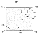
図3に示すのはセンサノードSN1の断面図である。この図に示されるように、基板BO1内部には、グランドプレーンGP1および電源プレーンVP1が設置されている。これら2つのプレーンは、基板BO1の表裏のシールドとして利用され、表面SIDE1に実装される高周波回路に伝達されるプロセッサチップCHIP2等から発生されるノイズを低減して実効的な受信感度を向上させる。グランドプレーンGP1は、グランド電位(基準電位)GNDに接続されたビア(例えばビアV20)に接続され、グランド電位GNDが与えられている。また、電源プレーンVP1は、電源ラインVDDに接続されたビア(例えばビアV10)に接続され、電源電位VDDが与えられている。図4および図5は、それぞれグランドプレーンGP1および電源プレーンVP1の平面構成を示した図である。グランドプレーンGP1では、グランドに接続しても良いビア(例えば、V20)以外の部分では、ビアに接触しないようにプレーン層を設置しない。図4に示す、電源電位VDDに接続されたビアを通すためのビア孔VH10〜15やインタフェースIF1を通すためのビア孔VHI1がこれに該当する。同様に、電源プレーンVP1においても電源プレーンVP1に接続しないビアの周囲にはプレーン層を設置しない(図5)。 FIG. 3 is a cross-sectional view of the sensor node SN1. As shown in this figure, a ground plane GP1 and a power plane VP1 are installed inside the board BO1. These two planes are used as shields for the front and back of the substrate BO1, and reduce noise generated from the processor chip CHIP2 and the like transmitted to the high-frequency circuit mounted on the surface SIDE1, thereby improving effective reception sensitivity. The ground plane GP1 is connected to a via (for example, via V20) connected to a ground potential (reference potential) GND, and is given a ground potential GND. The power supply plane VP1 is connected to a via (for example, the via V10) connected to the power supply line VDD, and is supplied with the power supply potential VDD. 4 and 5 are diagrams showing the planar configurations of the ground plane GP1 and the power supply plane VP1, respectively. In the ground plane GP1, a plane layer is not provided so as not to be in contact with a via in a portion other than a via (for example, V20) that may be connected to the ground. This corresponds to the via holes VH10 to VH10-15 for passing the vias connected to the power supply potential VDD and the via hole VHI1 for passing the interface IF1 shown in FIG. Similarly, in the power plane VP1, no plane layer is provided around a via that is not connected to the power plane VP1 (FIG. 5).
なお、図3では、2層のプレーン層のうちRFチップCHIP1に近い方のプレーン層をグランドプレーンGP1としているが、これは表面SIDE1上の高周波回路から見た場合のグランドプレーンGP1の電源インピーダンスを低くできることから好ましい構成である。また、図4、図5の例ではビア孔以外の全面にプレーン層を設けているが、裏面SIDE2または表面SIDE1の配線層としてその一部を用いることも可能である。 In FIG. 3, the plane layer closer to the RF chip CHIP1 out of the two plane layers is the ground plane GP1, but this is the power impedance of the ground plane GP1 when viewed from the high-frequency circuit on the surface SIDE1. This is a preferable configuration because it can be lowered. 4 and 5, the plane layer is provided on the entire surface other than the via hole. However, a part of the plane layer can be used as the wiring layer of the back surface SIDE2 or the front surface SIDE1.
次に、図2を参照しながら、基板BO1の裏面SIDE2に実装されたプロセッサチップCHIP2について説明する。プロセッサチップCHIP2は、メモリ回路MEM、プロセッサ回路CPU、データ入出力回路SIO、A/D変換回路ADC、タイミング生成回路TIM、プログラマブル入出力回路PIOを含む。これらの回路ブロックは、内部バスBU1により相互に結合され、データのやり取りや制御がなされる。 Next, the processor chip CHIP2 mounted on the back surface SIDE2 of the substrate BO1 will be described with reference to FIG. The processor chip CHIP2 includes a memory circuit MEM, a processor circuit CPU, a data input / output circuit SIO, an A / D conversion circuit ADC, a timing generation circuit TIM, and a programmable input / output circuit PIO. These circuit blocks are coupled to each other by an internal bus BU1 to exchange and control data.
メモリ回路MEMは低消費電力なSRAM(Static Random Access Memory)やフラッシュメモリ等の不揮発メモリで構成される。メモリ回路MEM上に、後述する本発明に特有な制御方式を実現するためのソフトウェアが搭載される。プロセッサ回路CPUは搭載されたソフトウェアに従ってプロセッサチップCHIP2内の他の回路ブロックを制御して、所望の動作を実現する。
データ入出力回路SIOはシリアルデータの入出力回路であり、センサデータをRFチップCHIP1に送るために使用される。また、プログラマブル入出力回路PIOはパラレルデータの入出力回路であり、主にRFチップCHIP1の送信/受信等の動作モードの制御に必要な制御データの入出力のために使用される。
The memory circuit MEM includes a low power consumption SRAM (Static Random Access Memory) and a nonvolatile memory such as a flash memory. On the memory circuit MEM, software for realizing a control method unique to the present invention, which will be described later, is mounted. The processor circuit CPU controls other circuit blocks in the processor chip CHIP2 in accordance with the installed software to realize a desired operation.
The data input / output circuit SIO is an input / output circuit for serial data, and is used to send sensor data to the RF chip CHIP1. The programmable input / output circuit PIO is an input / output circuit for parallel data, and is mainly used for input / output of control data necessary for controlling an operation mode such as transmission / reception of the RF chip CHIP1.
コネクタCN1には外部センサが接続されるが、外部センサはアナログデータを出力するものであっても、デジタルデータを出力するものであってもよい。アナログタイプのセンサのセンサデータAPはAD変換回路ADCによりデジタルデータに変換される。例えば、センサノードSN1にはアナログタイプの温度センサTS1が基板BO1上に内蔵されており、センサTS1からの温度データATはAD変換回路ADCにてデジタル量に変換され、必要に応じてメモリMEM上に格納される。一方、デジタルタイプのセンサデータDPはプログラマブル入出力回路PIOを介してプロセッサチップCHIP2に入力され、必要に応じてメモリMEM上に格納される。 An external sensor is connected to the connector CN1, and the external sensor may output analog data or digital data. The sensor data AP of the analog type sensor is converted into digital data by the AD conversion circuit ADC. For example, an analog type temperature sensor TS1 is built in the substrate BO1 in the sensor node SN1, and the temperature data AT from the sensor TS1 is converted into a digital quantity by the AD conversion circuit ADC and is stored in the memory MEM as necessary. Stored in On the other hand, the digital type sensor data DP is input to the processor chip CHIP2 via the programmable input / output circuit PIO, and stored in the memory MEM as necessary.
また、プロセッサチップCHIP2はRFSW/LNA制御回路LSCを制御し、増幅器LNAの電源のオン/オフや高周波スイッチRFSWの送受信切り替えを実行する。さらに、プロセッサチップCHIP2は電源遮断スイッチPS1,PS2を制御して、温度センサTS1や外部センサの電源のオン/オフを制御する。また、タイミング生成回路TIMは、水晶振動子X2またはX3の発振周波数から、動作に必要なタイミング、例えば、クロック信号や後述する間欠動作において使用されるタイマ信号が生成される。 Further, the processor chip CHIP2 controls the RFSW / LNA control circuit LSC to turn on / off the power supply of the amplifier LNA and switch transmission / reception of the high frequency switch RFSW. Further, the processor chip CHIP2 controls the power cutoff switches PS1 and PS2 to control the on / off of the power supply of the temperature sensor TS1 and the external sensor. The timing generation circuit TIM generates a timing required for operation, for example, a clock signal or a timer signal used in an intermittent operation described later, from the oscillation frequency of the crystal resonator X2 or X3.
なお、プロセッサチップCHIP2は、低消費電力動作のため2つの水晶振動子を使い分けている。水晶振動子X2はメインクロック用で、例えば、数MHz以上のものである。メインクロック使用時の消費電流は、典型的には数mAとなる。一方、水晶振動子X3は、サブクロックおよびタイマ信号の生成用で、例えば腕時計用に使用される32KHzの超低消費電力のタイプのもので構成される。プロセッサチップCHIP2は、低消費電力モードにおいてメインクロックX2を停止させ、サブクロックX3によりプロセッサチップを駆動することにより、消費電流を10μA以下に削減可能である。さらに、上記回路ブロックのうちAD変換回路ADC、データ入出力回路SIO、プログラマブル入出力回路PIO、メモリMEMは、プロセッサ回路CPUからの制御によりクロック供給を止めることにより、待機時の消費電流を低く抑え、数μA以下の待機電流を実現することができる。 Note that the processor chip CHIP2 uses two crystal resonators for low power consumption operation. The crystal resonator X2 is for a main clock, for example, having a frequency of several MHz or more. The current consumption when using the main clock is typically several mA. On the other hand, the crystal unit X3 is used to generate a subclock and a timer signal, and is composed of, for example, an ultra-low power consumption type of 32 KHz used for a wristwatch. The processor chip CHIP2 can reduce the current consumption to 10 μA or less by stopping the main clock X2 in the low power consumption mode and driving the processor chip with the sub clock X3. Further, among the above circuit blocks, the AD conversion circuit ADC, the data input / output circuit SIO, the programmable input / output circuit PIO, and the memory MEM suppress the current consumption during standby by stopping the clock supply under the control of the processor circuit CPU. A standby current of several μA or less can be realized.
次に、図1を参照しながら、基板BO1の表面SIDE1に実装されたRFチップCHIP1について説明する。RFチップCHIP1は、高周波変復調回路RF、発振回路OSC及び制御回路CONから構成される。プロセッサチップCHIP2から送られて来たセンサデータDSは高周波変復調回路RFにおいて所定の周波数帯(〜315MHz)の高周波無線信号RFOに変換され、外部無線端末へと送信される。また、外部無線端末からの高周波無線信号は、アンテナANT1にて受信され、高周波変復調回路RFにて復調される。復調された信号CSはインタフェースIF1経由でプロセッサチップCHIP2に引き渡される。なお、センサノードSN1では受信強度をモニタしており、受信強度を示す信号ASも高周波変復調回路RFのRSSI端子からインタフェースIF1経由でプロセッサチップCHIP2に引き渡されている。 Next, the RF chip CHIP1 mounted on the surface SIDE1 of the substrate BO1 will be described with reference to FIG. The RF chip CHIP1 includes a high frequency modulation / demodulation circuit RF, an oscillation circuit OSC, and a control circuit CON. The sensor data DS sent from the processor chip CHIP2 is converted into a high-frequency radio signal RFO in a predetermined frequency band (up to 315 MHz) by the high-frequency modulation / demodulation circuit RF and transmitted to an external radio terminal. A high frequency radio signal from the external radio terminal is received by the antenna ANT1, and demodulated by the high frequency modulation / demodulation circuit RF. The demodulated signal CS is delivered to the processor chip CHIP2 via the interface IF1. The sensor node SN1 monitors the reception intensity, and the signal AS indicating the reception intensity is also delivered from the RSSI terminal of the high frequency modulation / demodulation circuit RF to the processor chip CHIP2 via the interface IF1.
また、発振回路OSCは水晶振動子X1の発振周波数をベースに、RFチップCHIP1全体の動作に必要なクロック信号、及び目的の無線通信帯の高周波信号(搬送周波数信号)が生成される。
さらに、高周波変復調回路RFと発振回路OSCとは、制御回路CONにより、プロセッサチップCHIP2の制御信号CSに応じて制御される。具体的には、送信や受信等の動作モードの切り替えや、送受信信号の周波数帯の微調整、あるいは、送信電力等が制御される。さらに、プロセッサチップCHIP2からの制御信号により発振回路OSCを停止させて、RFチップCHIP1全体を待機状態に移行させることも可能である。この場合、RFチップCHIP1の消費電流を典型的には1μA以下にまで削減可能である。
その他の構成要素について動作及び構成を説明すると以下の通りである。
Further, the oscillation circuit OSC generates a clock signal necessary for the operation of the entire RF chip CHIP1 and a high-frequency signal (carrier frequency signal) of a target wireless communication band based on the oscillation frequency of the crystal resonator X1.
Further, the high frequency modulation / demodulation circuit RF and the oscillation circuit OSC are controlled by the control circuit CON in accordance with the control signal CS of the processor chip CHIP2. Specifically, switching of operation modes such as transmission and reception, fine adjustment of frequency bands of transmission / reception signals, transmission power, and the like are controlled. Further, it is possible to stop the oscillation circuit OSC by a control signal from the processor chip CHIP2 and shift the entire RF chip CHIP1 to a standby state. In this case, the current consumption of the RF chip CHIP1 can be reduced to typically 1 μA or less.
The operation and configuration of other components will be described as follows.
高周波スイッチRFSWは、裏面SIDE2上に設けられたRFSW/LNA制御回路LSCにより制御される。アンテナANT1とRFチップCHIP1との間の結線を切り替えて所望の送受信動作を実現する。具体的には、送信時には高周波スイッチRFSWのRI端子とRO2端子間を導通させる。また、受信時にはRI端子とRO1端子を導通させる。 The high frequency switch RFSW is controlled by an RFSW / LNA control circuit LSC provided on the back surface SIDE2. A desired transmission / reception operation is realized by switching the connection between the antenna ANT1 and the RF chip CHIP1. Specifically, at the time of transmission, the RI terminal and the RO2 terminal of the high frequency switch RFSW are made conductive. At the time of reception, the RI terminal and the RO1 terminal are made conductive.
増幅器LNAはRFチップCHIP1の外付けとして、アンテナANT1で受信された非常に微弱な高周波無線信号を、RFチップCHIP1で復調可能なレベルにまで増幅する。ここで、増幅器LNAを外付けとしたのは、RFチップCHIP1と違うプロセスで形成された素子を用いるためである。低コスト化及び低消費電力動作のため、RFチップCHIP1はCMOS回路で構成することが望ましい。しかし、その一方でCMOS回路にはゲート雑音が大きいといった問題があり、微弱な高周波無線信号を増幅するのは不得手である。そこで、増幅器LNAとしてはCMOSコンパチブルでないプロセスで形成された回路を用い、外付け回路としている。増幅器LNAはその増幅能力を考慮し、例えばGaAsといった化合物半導体、SiGe、あるいはバイポーラ回路で構成することが望ましい。アンテナANT1にて受信された高周波無線信号は、増幅器LNAの入力端子LIに入力され、所定の増幅率で増幅された後に出力端子LO経由で出力される。増幅器LNAの増幅率は、315MHz帯で10m程度の通信距離で安定的に通信したい場合には、10〜20dB程度が好ましい。また、増幅器は一般に消費電流が大きいため、イネーブル端子LEを制御することにより動作状態と待機状態とを切り替えるようにし、待機時の消費電流を典型的には10μA程度まで削減可能となっている。しかし、センサノードSN1において10μAもの電流を常時消費すると電池寿命に深刻な影響を与えるため、本実施例においてはプロセッサチップCHIP2からの制御によって増幅器LNAへの電源供給を遮断するように構成し、センサノードSN1の低消費電力化を図っている。 The amplifier LNA is externally attached to the RF chip CHIP1, and amplifies a very weak high-frequency radio signal received by the antenna ANT1 to a level that can be demodulated by the RF chip CHIP1. Here, the reason why the amplifier LNA is externally attached is to use an element formed by a process different from that of the RF chip CHIP1. The RF chip CHIP1 is preferably composed of a CMOS circuit for cost reduction and low power consumption operation. On the other hand, however, the CMOS circuit has a problem that the gate noise is large, and it is not good at amplifying a weak high-frequency radio signal. Therefore, as the amplifier LNA, a circuit formed by a process not compatible with CMOS is used, and an external circuit is used. The amplifier LNA is preferably composed of a compound semiconductor such as GaAs, SiGe, or a bipolar circuit in consideration of its amplification capability. The high-frequency radio signal received by the antenna ANT1 is input to the input terminal LI of the amplifier LNA, amplified by a predetermined amplification factor, and then output via the output terminal LO. The amplification factor of the amplifier LNA is preferably about 10 to 20 dB when it is desired to stably communicate at a communication distance of about 10 m in the 315 MHz band. Further, since the amplifier generally consumes a large amount of current, the operation state and the standby state are switched by controlling the enable terminal LE, and the current consumption during standby can be reduced to about 10 μA typically. However, if a current of 10 μA is constantly consumed in the sensor node SN1, the battery life is seriously affected. Therefore, in this embodiment, the power supply to the amplifier LNA is cut off by the control from the processor chip CHIP2. The power consumption of the node SN1 is reduced.
マッチング回路MAは、RFチップCHIP1の入出力インピーダンスと、高周波スイッチRFSWおよび増幅器LNAの入出力インピーダンスをマッチングさせ、高周波無線信号がこれらの素子の間でロスなく伝達できるようにするための回路である。マッチング回路MAは、インダクタ、コンデンサ、抵抗、あるいは、フィルタ等の受動部品で構成される。
図6は、表面SIDE1に実装された回路と裏面SIDE2に実装された回路とがインタフェースIF1を介して結線された状態を示す図である。インタフェースIF1は、データ信号線DS、制御信号線CS、表示装置(DISP)制御線DC、LNAイネーブル端子制御線LC、RFSW送受信切り替え制御線RC、および、電源ラインVDD/LNA電源ラインVDD1から構成される。
The matching circuit MA is a circuit for matching the input / output impedance of the RF chip CHIP1 with the input / output impedances of the high-frequency switch RFSW and the amplifier LNA so that a high-frequency radio signal can be transmitted between these elements without loss. . The matching circuit MA is composed of passive components such as an inductor, a capacitor, a resistor, or a filter.
FIG. 6 is a diagram illustrating a state where the circuit mounted on the front surface SIDE1 and the circuit mounted on the back surface SIDE2 are connected via the interface IF1. The interface IF1 includes a data signal line DS, a control signal line CS, a display device (DISP) control line DC, an LNA enable terminal control line LC, an RFSW transmission / reception switching control line RC, and a power supply line VDD / LNA power supply line VDD1. The
データ信号線DSは、プロセッサチップCHIP2のデータ入出力回路回路SIOとRFチップCHIP1の高周波変復調回路RF間を接続する信号線である。また、制御線信号CSは、プロセッサチップCHIP2のプログラマブル入出力回路PIOとRFチップCHIP1の制御回路CONとを接続する信号線である。データ信号線DSは2つのチップ間のデータのやり取りに使用され、制御信号線CSは、プロセッサチップCHIP2がRFチップCHIP1の動作モードを切り替えるための制御線として使用される。さらに、表示装置制御線DCは表示装置DISPの制御に用いられる。図7に表示装置DISPの構成例を示す。表示装置DISPは、発光ダイオードLD10、発光ダイオードLD10を駆動するインバータIV10及び発光ダイオードLD10の電流制限用の抵抗R10から構成される。表示装置DISPは、例えば、設置時に外部無線端末との無線通信に成功した時や、故障などの異常状態が生じた時に点灯し、表示装置制御線DCにより点灯あるいは消灯が制御される。 The data signal line DS is a signal line connecting the data input / output circuit circuit SIO of the processor chip CHIP2 and the high frequency modulation / demodulation circuit RF of the RF chip CHIP1. The control line signal CS is a signal line that connects the programmable input / output circuit PIO of the processor chip CHIP2 and the control circuit CON of the RF chip CHIP1. The data signal line DS is used for data exchange between the two chips, and the control signal line CS is used as a control line for the processor chip CHIP2 to switch the operation mode of the RF chip CHIP1. Further, the display device control line DC is used to control the display device DISP. FIG. 7 shows a configuration example of the display device DISP. The display device DISP includes a light emitting diode LD10, an inverter IV10 that drives the light emitting diode LD10, and a current limiting resistor R10 of the light emitting diode LD10. The display device DISP is turned on, for example, when the wireless communication with the external wireless terminal is successful at the time of installation, or when an abnormal state such as a failure occurs, and is turned on or off by the display device control line DC.
また、LNAイネーブル端子制御線LC、RFSW送受信切り替え制御線RC、および、LNA電源ラインVDD1は、RFSW/LNA制御回路LSCにより制御される。図8に、この制御回路LSCの構成例を示す。制御回路LSCの2つの入力端子LI1およびLI2は、プロセッサチップCHIP2のプログラマブル入出力回路PIOから出力される信号により制御される。増幅器LNAを起動する場合には、LI1を“0”に設定することにより電源遮断スイッチPS20を導通状態とし、増幅器LNAの電源ラインVDD1を通電する。このときLI2を“1”に設定すると、LNAイネーブル制御線LEを“0”に設定し、これにより増幅器LNAが活性化する。これとともに制御線LEと同じレベルをもつRFSW制御線RS−1が“0”に設定され、かつRFSW制御線RS−2がインバータIV21により“1”に設定されることにより、高周波スイッチRFSWは受信経路を導通させ、送信経路を遮断する。一方、LI2を“0”に設定すると、増幅器LNAは不活性とされ、かつ高周波スイッチRFSWは送信経路を導通させ、受信経路を遮断する。 The LNA enable terminal control line LC, the RFSW transmission / reception switching control line RC, and the LNA power supply line VDD1 are controlled by the RFSW / LNA control circuit LSC. FIG. 8 shows a configuration example of the control circuit LSC. The two input terminals LI1 and LI2 of the control circuit LSC are controlled by signals output from the programmable input / output circuit PIO of the processor chip CHIP2. When starting up the amplifier LNA, LI1 is set to “0” to turn on the power cut-off switch PS20, and the power supply line VDD1 of the amplifier LNA is energized. At this time, when LI2 is set to “1”, the LNA enable control line LE is set to “0”, thereby activating the amplifier LNA. At the same time, the RFSW control line RS-1 having the same level as the control line LE is set to “0”, and the RFSW control line RS-2 is set to “1” by the inverter IV21. The path is made conductive and the transmission path is blocked. On the other hand, when LI2 is set to “0”, the amplifier LNA is deactivated, and the high frequency switch RFSW conducts the transmission path and cuts off the reception path.
以下に本実施例の特徴をまとめる。
(1)微弱な高周波無線信号を扱う高周波回路とそれ以外のデジタル部分とを、基板BO1の表面と裏面とに分離してノイズの影響を低減して受信感度を向上させる。背景技術において説明したようにセンサノードを使用する際に最大送信電力に厳しい制約が課されている場合がある。このような場合には、RFチップ単体では受信感度が不足し、外付けの高周波低雑音増幅器LNAにより受信感度を補う必要がある。しかし、このような増幅器を設けても、デジタル部分からのノイズの回り込みを最小限に抑えないと増幅したい受信信号を増幅できない。ノイズの回り込みを抑えるため、このような場合にはRF部とデジタル部を距離的に離すのが一番効果的である。しかし、センサノードでは、サイズ、特に表面積を極力小さくすることが望ましく、高周波回路とデジタル回路との距離を大きくするために表面積が大きくなってしまうのは望ましくない。
The features of this embodiment are summarized below.
(1) A high-frequency circuit that handles a weak high-frequency radio signal and other digital parts are separated into a front surface and a back surface of the substrate BO1, thereby reducing the influence of noise and improving reception sensitivity. As described in the background art, when the sensor node is used, severe restrictions may be imposed on the maximum transmission power. In such a case, the RF chip alone has insufficient reception sensitivity, and it is necessary to supplement the reception sensitivity with an external high frequency low noise amplifier LNA. However, even if such an amplifier is provided, a received signal to be amplified cannot be amplified unless noise wraparound from the digital portion is minimized. In such a case, it is most effective to separate the RF unit and the digital unit from each other in order to suppress noise wraparound. However, in the sensor node, it is desirable to reduce the size, particularly the surface area as much as possible, and it is not desirable that the surface area be increased in order to increase the distance between the high-frequency circuit and the digital circuit.
そこで、高周波回路とデジタル回路とを基板の表裏で分離し、基板内部にノイズ信号のシールドに効果的なグランドプレーン及び電源プレーンを設置する。まず、デジタル回路からのノイズがこのグランドプレーンでシールドされ、RF部への回り込みを極力抑えることが可能となる。さらに、グランドプレーンの直下に電源プレーンを配置することによって電源プレーンとグランドプレーン間に静電容量を持たせることが可能となる。この静電容量はデジタル回路から電源回路に回り込む可能性のあるノイズを吸収するのに効果的なバイパスコンデンサとして利用できる。この静電容量により電源回路を経由してデジタル回路から高周波回路へ回り込む可能性のあるノイズを最小限に抑えることが可能になる。特に、電源プレーンやグランドプレーンを基板BO1に可能な限り一面に広げる事で、電源部のインピーダンスを小さく抑える事が可能となる。この結果、たとえ、多少のデジタル回路からのノイズが高周波回路に回り込んだとしても、電源インピーダンスが低く抑えられているので、ノイズ成分の電圧振幅を小さく抑えることが可能となる。これは、ノイズ電圧は、回り込んだノイズ電流と電源インピーダンスの積で表されるためである。以上により、たとえデジタル回路から高周波回路へ多少のノイズが回り込んだとしても高周波回路を誤動作させてしまう、あるいは、アンテナからの微弱なRF信号をマスクしてしまう程度のレベル以下に抑え込むことが可能となる。 Therefore, the high-frequency circuit and the digital circuit are separated from each other on the front and back of the board, and a ground plane and a power plane effective for shielding noise signals are installed inside the board. First, noise from the digital circuit is shielded by this ground plane, and the wraparound to the RF section can be suppressed as much as possible. Furthermore, it is possible to provide a capacitance between the power plane and the ground plane by arranging the power plane immediately below the ground plane. This electrostatic capacity can be used as a bypass capacitor that is effective in absorbing noise that may circulate from the digital circuit to the power supply circuit. With this electrostatic capacity, it is possible to minimize noise that may circulate from the digital circuit to the high-frequency circuit via the power supply circuit. In particular, it is possible to reduce the impedance of the power supply unit by spreading the power supply plane and the ground plane as much as possible on the board BO1. As a result, even if some noise from the digital circuit circulates into the high frequency circuit, the power supply impedance is kept low, so that the voltage amplitude of the noise component can be kept small. This is because the noise voltage is represented by the product of the sneak noise current and the power source impedance. As a result, even if some noise circulates from the digital circuit to the high-frequency circuit, the high-frequency circuit can malfunction, or the level can be suppressed to a level that masks the weak RF signal from the antenna. It becomes.
本実施例では、基板の表面と裏面の両面で高密度で部品を実装する場合において、さらに受信感度を向上させるように、単に実装面を分離するのみならず、各実装面における配置位置にも工夫を行った。図1および図2にも示されるように、本実施例においては、RFチップの入力、増幅器LNA、高周波スイッチRFSW、及びアンテナANT1といった、高周波回路の中でもレベルが微弱な高周波無線信号を扱う部分を、デジタル回路の中でもデジタル信号が頻繁に“0”/“1”間を遷移し、ノイズ発生量の大きい回路からはできる限り遠ざける配置を取る。図9は、この構造をわかりやすく説明した図である。 In this embodiment, when components are mounted at high density on both the front and back surfaces of the board, the mounting surface is not only separated but also arranged at each mounting surface so as to further improve reception sensitivity. Devised a device. As shown in FIGS. 1 and 2, in this embodiment, the RF chip input, the amplifier LNA, the high frequency switch RFSW, and the antenna ANT1 handle portions that handle high-frequency radio signals with weak levels in the high-frequency circuit. In the digital circuit, the digital signal frequently transits between “0” / “1”, and is arranged as far as possible from the circuit having a large noise generation amount. FIG. 9 is a diagram illustrating this structure in an easy-to-understand manner.
図9に示されるように、アンテナANT1にて受信された微弱な高周波無線信号RFS1は高周波スイッチRFSWに入力される。高周波スイッチRFSWにて選択され、幾分か減衰した高周波無線信号RFS2は、増幅器LNAに入力され、所定の増幅率で増幅される。増幅された高周波無線信号RFS3はマッチング回路MAに導かれ、インピーダンスマッチングされた高周波無線信号RFS4は、RFチップCHIP1に入力される。RFチップCHIP1内では、高周波無線信号RFS4はデジタル信号DJS1に復調され、インタフェースIF1経由でプロセッサチップCHIP2に取り込まれる。 As shown in FIG. 9, the weak high frequency radio signal RFS1 received by the antenna ANT1 is input to the high frequency switch RFSW. The high-frequency radio signal RFS2 selected by the high-frequency switch RFSW and somewhat attenuated is input to the amplifier LNA and amplified at a predetermined amplification factor. The amplified high-frequency radio signal RFS3 is guided to the matching circuit MA, and the impedance-matched high-frequency radio signal RFS4 is input to the RF chip CHIP1. In the RF chip CHIP1, the high-frequency radio signal RFS4 is demodulated into a digital signal DJS1 and taken into the processor chip CHIP2 via the interface IF1.
無線LANといったような無線通信機器では、一般にデジタル信号で通信するためのコネクタは、パソコン本体とデジタル信号をやりとりするといった用途に用いられるために、コネクタには、高い頻度で“0”/“1”間を遷移する、すなわち高速なデジタル信号がやり取りされる。このため、コネクタをアンテナとを距離的に離すようにさせた例がある。これに対して、本実施例のセンサノードSN1では、コネクタCN1には外部センサが接続され、コネクタCN1とプロセッサチップCHIP2間でやり取りされる信号DJP1は遷移の非常にゆっくりしたアナログ信号、またはプロセッサチップCHIP2のクロック信号よりも低速なデジタル信号である。そこで、本実施例ではコネクタCN1をアンテナANT1〜RFチップCHIP1の信号経路に近い位置に配置し、プロセッサチップCHIP2をアンテナANT1〜RFチップCHIP1の信号経路により遠い位置に配置することとしたものである。表現を変えれば、コネクタCN1とRFチップCHIP1との距離が、プロセッサチップCHIP2とRFチップCHIP1との距離よりも長くなるようにコネクタCN1を配置するようにするものである。このように、図9に示す部品配置はセンサノード特有の信号の流れをうまく捉えて、サイズ小型化と受信感度の向上の両方を同時に実現可能な部品配置となっている。 In a wireless communication device such as a wireless LAN, a connector for communicating with a digital signal is generally used for the purpose of exchanging a digital signal with a personal computer body. Therefore, the connector is frequently “0” / “1”. "Transition between, that is, high-speed digital signals are exchanged. For this reason, there is an example in which the connector is separated from the antenna by a distance. On the other hand, in the sensor node SN1 of the present embodiment, an external sensor is connected to the connector CN1, and the signal DJP1 exchanged between the connector CN1 and the processor chip CHIP2 is an analog signal having a very slow transition, or a processor chip. The digital signal is slower than the clock signal of CHIP2. Therefore, in this embodiment, the connector CN1 is arranged at a position close to the signal path of the antennas ANT1 to RF chip CHIP1, and the processor chip CHIP2 is arranged at a position far from the signal path of the antennas ANT1 to RF chip CHIP1. . In other words, the connector CN1 is arranged so that the distance between the connector CN1 and the RF chip CHIP1 is longer than the distance between the processor chip CHIP2 and the RF chip CHIP1. As described above, the component arrangement shown in FIG. 9 is a component arrangement that can grasp both the signal flow specific to the sensor node and realize both the size reduction and the improvement of the reception sensitivity at the same time.
(2)高周波低雑音増幅器LNAの電源線に電源遮断スイッチ(図1、2、8を参照)挿入し、待機時の消費電流を抑える。高周波低雑音増幅器LNAは、一般に消費電力が大きく、待機時でも10μA程度の電流を消費する。この電流値は、サイズや用途の制約から十分な電源を得られないセンサノードにとっては大きすぎる値である。しかし、増幅器LNA無しに実用的な通信距離が達成不可能な場合もある。 (2) Insert a power cut-off switch (see FIGS. 1, 2 and 8) into the power line of the high-frequency low-noise amplifier LNA to suppress current consumption during standby. The high-frequency low-noise amplifier LNA generally consumes a large amount of power, and consumes a current of about 10 μA even during standby. This current value is too large for a sensor node that cannot obtain a sufficient power supply due to size and application restrictions. However, there are cases where a practical communication distance cannot be achieved without the amplifier LNA.
そこで、図8に示したように、増幅器LNAの電源線に電源遮断スイッチPS20を挿入して、このPS20により待機時の消費電流を削減する。この電源遮断スイッチは、図10(a)〜(e)に示すように、(a)P―MOSFET MP1で構成したもの、(b)PNPバイポーラトランジスタBP1で構成したもの、(c)N−MOSFET MN1で構成したもの、(d)NPNバイポーラトランジスタBN1で構成したもの、(e)プログラマブル入出力回路PIO出力をそのまま利用する等、様々なタイプが使用可能である。いずれのタイプも、プロセッサチップCHIP2のプログラマブル入出力回路PIOの出力端子から駆動される制御端子SC1〜5を“1”あるいは“0”に設定すれば、LNAへの電源供給を遮断できる。実際には、スイッチング素子MP1〜BN1のオフ時にも若干の漏れ電流が流れるものの、カタログ値で0.1μA以下のオーダーであり、このようなオフ時の漏れ電流は電池寿命にはほとんど影響を与えないと考えて良い。 Therefore, as shown in FIG. 8, a power cutoff switch PS20 is inserted into the power line of the amplifier LNA, and the current consumption during standby is reduced by this PS20. As shown in FIGS. 10A to 10E, the power cut-off switch is composed of (a) a P-MOSFET MP1, (b) a PNP bipolar transistor BP1, (c) an N-MOSFET. Various types can be used, such as those configured with MN1, (d) configured with NPN bipolar transistor BN1, and (e) using the programmable I / O circuit PIO output as it is. In any type, when the control terminals SC1 to SC5 driven from the output terminal of the programmable input / output circuit PIO of the processor chip CHIP2 are set to “1” or “0”, the power supply to the LNA can be cut off. Actually, although some leakage current flows even when the switching elements MP1 to BN1 are turned off, the catalog value is on the order of 0.1 μA or less, and such leakage current at the time of turning off has little influence on the battery life. You can think of it not.
一方、動作時には、これらスイッチング素子MP1〜BN1の内部抵抗により若干の電圧降下が発生する。しかし、例えば、図10(a)のタイプだと、スイッチング素子MP1がオンした場合の内部抵抗が5Ω程度のものとできる。既に述べたように、増幅器LNAの動作時の消費電流は10mA程度であり、スイッチング素子MP1に起因する電圧降下は50mV(=5Ω×10mA)程度となり、無視できる程度の値である。なお、図10(e)に示すように、プロセッサチップCHIP2のプログラマブル入出力回路PIOの出力ドライブ能力に十分に余裕がある場合、すなわち、動作時に必要な電流値以上の電流値を十分に供給可能な場合には、図10(a)〜(d)に示すようなスイッチング素子なしで、増幅器LNAの電源を駆動することも可能であろう。 On the other hand, during operation, a slight voltage drop occurs due to the internal resistance of these switching elements MP1 to BN1. However, for example, in the type of FIG. 10A, the internal resistance when the switching element MP1 is turned on can be about 5Ω. As already described, the current consumption during the operation of the amplifier LNA is about 10 mA, and the voltage drop caused by the switching element MP1 is about 50 mV (= 5Ω × 10 mA), which is a negligible value. As shown in FIG. 10 (e), when the output drive capability of the programmable input / output circuit PIO of the processor chip CHIP2 has a sufficient margin, that is, it is possible to supply a current value higher than the current value necessary for operation. In that case, it would be possible to drive the power source of the amplifier LNA without the switching elements as shown in FIGS.
このように本実施例では、増幅器LNAを使わない時(受信時以外)では、電源遮断スイッチPS20を遮断状態に遷移させ、増幅器LNAを使う時(受信時)では、電源遮断スイッチPS20を導通状態に遷移させる。実際には、電源遮断スイッチを遮断状態から導通状態に遷移させても、増幅器LNAの内部回路が安定するのを待つ必要があり、典型的には1ms程度要する。しかし、一般にはセンサノードSN1は待機時間が動作時間に比べて非常に長い、場合によっては動作時間は全体の約1%程度と想定されているため、受信状態への切り替え待ち時間に起因する消費電力の増加分は無視してよい。
(3)センサ(内蔵及び外付け)の電源線に電源遮断スイッチ(図2を参照)挿入し、待機時の消費電流を抑える。本実施例の第2の特徴と同様の原理をセンサの待機時の消費電流の削減に応用したものといえる。例えば、図2に示すように内蔵温度センサTS1の電源線VDD2は電源遮断スイッチPS1により温度センサTS1の未使用時には電源を遮断できる。現在、温度センサには低消費電力のタイプ(消費電流が5μA程度)のものが開発されており、電源遮断スイッチPS1としては図10(e)のようなタイプでも動作に必要な電流を十分に供給可能である。図10(e)のタイプは、追加のディスクリート素子が不要であり、追加コスト無しに実現できる。
As described above, in this embodiment, when the amplifier LNA is not used (except during reception), the power cutoff switch PS20 is shifted to the cutoff state, and when the amplifier LNA is used (during reception), the power cutoff switch PS20 is in the conduction state. Transition to. Actually, even when the power cut-off switch is changed from the cut-off state to the conductive state, it is necessary to wait for the internal circuit of the amplifier LNA to be stabilized, which typically takes about 1 ms. However, in general, the sensor node SN1 has a very long standby time compared to the operation time. In some cases, the operation time is assumed to be about 1% of the entire operation time. The increase in power can be ignored.
(3) Insert a power cut-off switch (see Fig. 2) into the power line of the sensor (built-in and external) to reduce current consumption during standby. It can be said that the same principle as the second feature of this embodiment is applied to reduction of current consumption during standby of the sensor. For example, as shown in FIG. 2, the power supply line VDD2 of the built-in temperature sensor TS1 can be cut off by the power cut-off switch PS1 when the temperature sensor TS1 is not used. At present, a temperature sensor of a low power consumption type (current consumption is about 5 μA) has been developed, and the power cut-off switch PS1 has sufficient current necessary for operation even with the type as shown in FIG. 10 (e). It can be supplied. The type shown in FIG. 10E does not require an additional discrete element and can be realized without additional cost.
また、外付けセンサの消費電力を削減するため、外付けセンサを接続するコネクタCN1の電源ラインVDD3も電源遮断スイッチPS2により遮断する(図2を参照)。一般に、外付けのセンサの消費電力は、内蔵温度センサよりも待機時および動作時ともに大きい。例えば、加速度センサには1mAもの消費電流を要するものもあり、また、外付けセンサ自身には待機状態に移行する機能がない場合が多い。そのため、本実施例のように電源遮断スイッチを使用しなければ、ボタン電池では1週間程度(8.3日=200mAh/1mA/24h)の動作寿命しか得られないものと予想される。さらに大電流で放電した場合の電池容量の劣化現象が生じた場合には、せいぜい数日しか持たないものと予想される。これに対して、電源遮断スイッチにより使用時のみ電源供給を行い、未使用時には電源を遮断することにより、電池寿命を飛躍的に向上させる事が可能となる。 In order to reduce the power consumption of the external sensor, the power supply line VDD3 of the connector CN1 connecting the external sensor is also shut off by the power shutoff switch PS2 (see FIG. 2). In general, the power consumption of an external sensor is larger during both standby and operation than the built-in temperature sensor. For example, some acceleration sensors require a current consumption of 1 mA, and the external sensor itself often does not have a function of shifting to a standby state. Therefore, it is expected that the operation life of about one week (8.3 days = 200 mAh / 1 mA / 24 h) can be obtained with a button battery unless a power cut-off switch is used as in this embodiment. Furthermore, if the battery capacity deteriorates when discharged with a large current, it is expected that the battery has only a few days. On the other hand, it is possible to drastically improve the battery life by supplying power only when using the power cutoff switch and shutting off the power when not in use.
この構成は、外付けセンサが何らかの原因で、ショートモードで故障してしまった場合にも有効である。すなわち、外付けセンサがショートモードで故障してしまうと、外付けセンサの電源の電源遮断を行わない場合には、瞬時のうちに電池から大電流が流れて電池を使い切ってしまう。しかし、本実施例では外付けセンサ電源は通常はオフ状態にあり、センサを使用する場合のみ電源が投入されるよう構成されている。さらに、電源は電源遮断スイッチを構成するスイッチング素子を介して供給されるため、スイッチング素子のオン抵抗により、ショート時の電流も低く抑えられ、かつ、ショートにより大電流が流れることにより、電池の内部抵抗による電圧降下が発生して、スイッチング素子がオン状態を保持するために必要なバイアス電圧が確保できなくなり、電源遮断スイッチは自動的にオフ状態に戻る。 This configuration is also effective when the external sensor has failed in the short mode for some reason. That is, if the external sensor fails in the short mode, if the power supply of the external sensor is not shut off, a large current flows from the battery instantaneously and the battery is used up. However, in this embodiment, the external sensor power supply is normally in an off state, and the power is turned on only when the sensor is used. Furthermore, since the power is supplied through the switching element that constitutes the power cutoff switch, the on-resistance of the switching element reduces the current at the time of the short circuit, and a large current flows due to the short circuit. A voltage drop due to the resistance occurs, and it becomes impossible to secure a bias voltage necessary for the switching element to maintain the on state, and the power shut-off switch automatically returns to the off state.
この間にプロセッサチップCHIP2は、内蔵のAD変換回路ADC経由で外付けセンサの出力値を読み込みに行くのであるが、ショート状態であるので“0”電位付近に張り付いたままの異常値しか読み出せない。そこで、プロセッサチップ搭載の制御ソフトウェアに、このような場合には異常と判断して異常信号を無線送信する、という機能をもたせておけば、当該センサノードの外付けセンサが動作不良に陥った事を外部から検出可能である。さらに、異常信号を検出したシステムでは、当該センサノードに、外付けセンサの使用を中断する旨の制御コマンドを発行して、問題の生じた外付けのセンサを使用しないようにしてセンサノードの動作を継続させる事も可能である。さらに、後述するようにプロセッサチップCHIP2のメモリ回路MEM1に格納されたID番号から、外付けセンサが故障したセンサノードを割り出すことができれば交換等の対処も可能となる。 During this time, the processor chip CHIP2 reads the output value of the external sensor via the built-in AD converter circuit ADC. However, since it is in a short circuit state, it can read only the abnormal value that remains stuck near the “0” potential. Absent. Therefore, if the control software installed in the processor chip has a function to judge that there is an abnormality in this case and transmit an abnormal signal wirelessly, the external sensor of the sensor node has become defective. Can be detected from the outside. Furthermore, in a system that detects an abnormal signal, issue a control command to the sensor node to interrupt the use of the external sensor, and operate the sensor node so as not to use the external sensor that caused the problem. It is also possible to continue. Further, as will be described later, if the sensor node in which the external sensor has failed can be determined from the ID number stored in the memory circuit MEM1 of the processor chip CHIP2, it is possible to cope with replacement or the like.
次に、動作時の消費電流によるボタン電池の電池容量の劣化現象を回避するための、電力制御方法について詳細に説明する(図11参照)。センサノードは、ノードをセットして起動(P100)後、初期設定ルーチン(P110)を実行すると、ただちに待機ルーチン(P120)に移行する。初期設定ルーチンP110では、あらかじめプロセッサチップCHIP2のメモリ回路MEM内の不揮発メモリ部分に格納された動作のパラメータ等を格納したPDATAファイルに基づいて、センサノードの動作モードを所望の状態に設定する。PDATAファイルには、例えば、どのくらいの時間間隔で待機状態から動作状態に移行するかのタイマ間隔、無線通信の伝送レート、使用する周波数帯、およびセンサノード毎に固有の番号を割り振ったID番号等の情報が格納される。さらに、後述する動作モード判定ルーチン(P200)で使用される、増幅器LNA、RFチップCHIP1、プロセッサチップCHIP2、外付けセンサ等の消費電流値もPDATAファイルに格納される。なお、初期設定ルーチンP110では、プロセッサチップCHIP2は低消費電力モードで動作し、プロセッサチップCHIP2のメインクロックX2、RFチップCHIP1のクロックX1もオフする。また、センサや増幅器LNAへの電源供給も遮断されている。 Next, a power control method for avoiding the deterioration phenomenon of the battery capacity of the button battery due to current consumption during operation will be described in detail (see FIG. 11). When the sensor node sets and starts the node (P100) and then executes the initial setting routine (P110), the sensor node immediately shifts to the standby routine (P120). In the initial setting routine P110, the operation mode of the sensor node is set to a desired state based on the PDATA file storing the operation parameters stored in advance in the nonvolatile memory portion in the memory circuit MEM of the processor chip CHIP2. The PDATA file includes, for example, a timer interval indicating how long a transition is made from a standby state to an operating state, a wireless communication transmission rate, a frequency band to be used, an ID number assigned a unique number for each sensor node, etc. Is stored. Further, current consumption values of the amplifier LNA, the RF chip CHIP1, the processor chip CHIP2, the external sensor, etc. used in an operation mode determination routine (P200) described later are also stored in the PDATA file. In the initial setting routine P110, the processor chip CHIP2 operates in the low power consumption mode, and the main clock X2 of the processor chip CHIP2 and the clock X1 of the RF chip CHIP1 are also turned off. The power supply to the sensor and the amplifier LNA is also cut off.
待機ルーチンP120では、プロセッサチップCHIP2内のタイミング生成回路TIMのみ動作状態となり、動作する部分を必要最小限に抑える。このように設定する事で、待機時の動作電流を数μA、典型的には5μA以下までに削減可能である。なお、初期設定ルーチンP110で設定したタイマ間隔で発生するタイマ割り込みが発生すると、次のCPU起動ルーチン(P130)に移行する。また、コネクタCN1(図2)にプロセッサチップの割り込み線を接続しておけば、外部からの割り込みにより、オンデマンドで、センサノードを起動させることも可能である。
CPU起動ルーチンP130により、プロセッサチップCHIP2のメインクロックX2をオンにして、CHIP2内のプロセッサ回路CPUを起動する。起動後、動作モード決定ルーチン(P200)に移行する。
In the standby routine P120, only the timing generation circuit TIM in the processor chip CHIP2 is in an operating state, and the operating portion is minimized. By setting in this way, the standby operating current can be reduced to several μA, typically 5 μA or less. If a timer interrupt occurs at the timer interval set in the initial setting routine P110, the process proceeds to the next CPU activation routine (P130). If the interrupt line of the processor chip is connected to the connector CN1 (FIG. 2), the sensor node can be activated on demand by an external interrupt.
By the CPU activation routine P130, the main clock X2 of the processor chip CHIP2 is turned on to activate the processor circuit CPU in the CHIP2. After startup, the process proceeds to an operation mode determination routine (P200).
動作モード決定ルーチンP200では、パラメータ/コマンド解析サブルーチン(P220)により、既に説明したPDATAファイルから、デバイス毎の消費電流を読み込む。この際に、外部無線端末から送られて来て受信されたコマンド、例えばセンサデータの送信リクエスト等を読み込むこともできる。コマンドは、例えば、「温度センサを起動してその結果を送信せよ」といったものになる。次に読み込まれたパラメータおよびコマンドを元に、消費電流推定サブルーチン(P230)において、実行に必要な消費電流を推定する。スケジューラサブルーチン(P210)において、基地局から要求されたリクエストを満たした上で、消費電流のピーク値がもっとも小さくなるように、以下に続く、センシングルーチン(P300)、および、データ送受信ルーチン(P400)の起動方式を決定する。 In the operation mode determination routine P200, the current consumption for each device is read from the PDATA file already described by the parameter / command analysis subroutine (P220). At this time, it is also possible to read a command received from an external wireless terminal, such as a sensor data transmission request. The command is, for example, “activate the temperature sensor and send the result”. Next, based on the read parameters and commands, the current consumption necessary for execution is estimated in the current consumption estimation subroutine (P230). In the scheduler subroutine (P210), the following sensing routine (P300) and data transmission / reception routine (P400) are performed so that the peak value of current consumption becomes the smallest after satisfying the request requested from the base station. Determine the startup method.
例えば、センシングルーチンP300にて、動作時の消費電流が数mA程度で、データの送受信に必要な消費電流(10mA〜20mA)と比較して無視できない外部センサを起動する場合には、データ送受信ルーチンP400を同時には起動しない。図12に示すのが、この場合のセンサノードの典型的な消費電流の波形である。一方、起動するセンサが内蔵温度センサ等で数μA程度電流しか消費しないセンサの場合には、データ送受信ルーチンP400を同時起動する。図13に示すのが、この場合に対応する、センサノードの典型的な消費電流波形である。このような電力制御により、消費電流のピーク値を低減することが可能となる。 For example, in the sensing routine P300, when starting an external sensor whose current consumption during operation is about several mA and cannot be ignored compared with the current consumption (10 mA to 20 mA) necessary for data transmission / reception, the data transmission / reception routine P400 is not activated simultaneously. FIG. 12 shows a typical current consumption waveform of the sensor node in this case. On the other hand, when the sensor to be activated is a built-in temperature sensor or the like that consumes only about several μA of current, the data transmission / reception routine P400 is simultaneously activated. FIG. 13 shows a typical current consumption waveform of the sensor node corresponding to this case. Such power control makes it possible to reduce the peak value of current consumption.
センシングルーチンP300の動作は以下の通りである。まず、外部/内蔵センサ判定サブルーチン(P310)にて、起動するセンサの種別を判定する。次にセンサ電源起動サブルーチン(P320)により、内蔵センサならばPS1をオンに設定し、外部センサならばPS2をオンに設定する。次に、ポートオープンサブルーチン(P330)において、内蔵あるいは外部センサのセンサ結果を読み出すのに必要なポートがオープンされる。例えば、図2に示す内蔵温度センサTS1を読み取る場合には、プロセッサチップCHIP2のAD変換回路ADCが起動され、ADCの入力端子I2が読み込み可能状態に設定される。また、起動したいセンサが、図2で示すコネクタCN1に接続された外部センサの時には、対応するAD変換回路ADCの入力端子、あるいは、プログラマブル入出力回路PIOの入出力端子が所望の動作モードへと設定される。このようにしてセンサからのデータを読み取り可能な状態に設定される。そして、次のセンサデータ読み出し/書き出しサブルーチン(P340)にて、実際にセンサデータがプロセッサチップCHIP2に読み取られ、メモリ回路MEM上のファイルSDATAに格納される。以上の手順で所望のセンサデータをファイルSDATA内に書き出したら、次のポートクローズ/ADCオフサブルーチン(P350)にて、使用したAD変換回路ADCやプログラマブル入出力回路PIOを待機状態に移行させて、センシングルーチンP300を終了する。 The operation of the sensing routine P300 is as follows. First, the type of sensor to be activated is determined in the external / internal sensor determination subroutine (P310). Next, according to the sensor power supply startup subroutine (P320), PS1 is set to ON for an internal sensor, and PS2 is set to ON for an external sensor. Next, in a port open subroutine (P330), a port necessary for reading the sensor result of the internal or external sensor is opened. For example, when reading the built-in temperature sensor TS1 shown in FIG. 2, the AD conversion circuit ADC of the processor chip CHIP2 is activated, and the input terminal I2 of the ADC is set in a readable state. When the sensor to be activated is an external sensor connected to the connector CN1 shown in FIG. 2, the input terminal of the corresponding AD conversion circuit ADC or the input / output terminal of the programmable input / output circuit PIO enters the desired operation mode. Is set. In this way, the data from the sensor can be read. Then, in the next sensor data read / write subroutine (P340), the sensor data is actually read by the processor chip CHIP2 and stored in the file SDATA on the memory circuit MEM. After the desired sensor data is written in the file SDATA by the above procedure, the used AD conversion circuit ADC or programmable input / output circuit PIO is shifted to a standby state in the next port close / ADC off subroutine (P350). The sensing routine P300 ends.
次に、データ送受信ルーチンP400の動作を説明する。まず第1に、クロックX1オンサブルーチン(P410)にて、RFチップCHIP1のクロックX1を立ち上げ、RFチップCHIP1を起動する。この際、プロセッサチップCHIP2によるRFチップCHIP1の起動は、既に説明した制御信号線CS経由でRFチップ規定の形式で行う。次に送受信動作判定サブルーチン(P420)により、送信か受信かどちらかの動作が必要かを判断する。このルーチンでは、例えば、最初にセンサノードから基地局へとセンサデータを送信し、その後センサノードは受信状態に移行する。センサノードは、送信したセンサデータを基地局が誤り無く受信したという確認信号が基地局から送り返されて来るまで受信状態で待機する。以上のシーケンスの制御は、サブルーチンP420にて実行される。以下、送信および受信動作について説明する。 Next, the operation of the data transmission / reception routine P400 will be described. First, in the clock X1 on subroutine (P410), the clock X1 of the RF chip CHIP1 is raised and the RF chip CHIP1 is activated. At this time, the activation of the RF chip CHIP1 by the processor chip CHIP2 is performed in the form prescribed by the RF chip via the control signal line CS already described. Next, a transmission / reception operation determination subroutine (P420) determines whether transmission or reception is necessary. In this routine, for example, sensor data is first transmitted from the sensor node to the base station, and then the sensor node shifts to a reception state. The sensor node stands by in a reception state until a confirmation signal that the base station has received the transmitted sensor data without error is sent back from the base station. The above sequence control is executed in subroutine P420. Hereinafter, transmission and reception operations will be described.
送信動作の場合には、サブルーチンP430により、高周波スイッチRFSWを送信状態に切り替える。また、RFチップCHIP1に制御信号線CS経由で使用する伝送レートや周波数帯等の通信パラメータを送る。次に、サブルーチンP440により、メモリMEM上のファイルSDATAからセンサデータを読み出して、データ信号線DS経由でRFチップCHIP1に送って、センサデータを外部に無線通信により送信する。
受信動作の場合には、サブルーチンP450により、高周波スイッチRFSWやRFチップCHIP1の通信パラメータの設定を行うとともに、LNA電源遮断スイッチPS20を導通状態に設定し、さらに、LNAのイネーブル端子を活性化させる。次に、サブルーチンP460にてデータを受信し、必要に応じてPDATA内に書き込む。
In the case of the transmission operation, the high frequency switch RFSW is switched to the transmission state by a subroutine P430. In addition, communication parameters such as a transmission rate and a frequency band used via the control signal line CS are sent to the RF chip CHIP1. Next, by the subroutine P440, the sensor data is read from the file SDATA on the memory MEM, sent to the RF chip CHIP1 via the data signal line DS, and the sensor data is transmitted to the outside by wireless communication.
In the case of the reception operation, the communication parameters of the high frequency switch RFSW and the RF chip CHIP1 are set by the subroutine P450, the LNA power cut-off switch PS20 is set to the conductive state, and the LNA enable terminal is activated. Next, data is received in subroutine P460 and written in PDATA as necessary.
なお、以上の説明では簡略化のため省略したが、実際には、増幅器LNAの起動や、高周波スイッチRFSWの切り替え、さらには、RFチップCHIP1のクロックX1の起動には、それぞれ安定するまでに時間(典型的には、数100μs〜数ms)が必要なため、それぞれのルーチンにてその時間分だけ待つ処理が必要である。同様に、増幅器LNAの電源オフやRFチップCHIP1のクロックオフにも安定化するまでには時間が必要であり、待ち時間処理が必要である。 Although omitted in the above description for the sake of simplification, in actuality, it takes time to stabilize the activation of the amplifier LNA, the switching of the high-frequency switch RFSW, and the activation of the clock X1 of the RF chip CHIP1. Since (typically, several hundred μs to several ms) is required, processing for waiting for that time is required in each routine. Similarly, it takes time to stabilize the power-off of the amplifier LNA and the clock-off of the RF chip CHIP1, and waiting time processing is necessary.
最後に基地局からの受信確認信号が受信されたら、サブルーチンP470にて、クロックX1を停止して、RFチップCHIP1をオフ状態に戻す。さらに、サブルーチンP140にて、プロセッサチップCHIP2のメインクロックX2を停止して、待機ルーチンP120へと移行する。 When the reception confirmation signal is finally received from the base station, the clock X1 is stopped and the RF chip CHIP1 is returned to the OFF state in subroutine P470. Further, in the subroutine P140, the main clock X2 of the processor chip CHIP2 is stopped, and the process proceeds to the standby routine P120.
このように、本実施例においては事前に必要な消費電流を判断して、ボタン電池の電流容量を劣化させない方式を選択する。すなわち、センサが数mAもの消費電流を消費する場合に、データ送受信とセンサを同時に起動してしまっては、ボタン電池には電池容量を深刻に劣化させかねない重い負荷を与えてしまう。図14に示すのが、この場合の消費電流の波形例である。図12に示す、本発明の制御方式を適用した場合よりも、ピーク電流(Ip3)はかなり大きな値になってしまう(Ip3>Ip1)。一方、図12と図14を比較すれば明らかなように、図12の制御方式では、センサを起動した後にデータの送受信を行うため、一連の処理を終了するのに必要な時間は長くなってしまう(Ttotal1>Ttotal3)。また、平均消費電流は図12の場合の方が幾分か大きい。しかし、センサノードSN1の電源としてCR2032等のボタン電池を用いる場合には、電池容量を劣化させない範囲で使用できる消費電流は、せいぜい0.1mAのオーダーである。一方、センサノードの動作には10mAのオーダーの電流が必要である。しかし、このような電流値でボタン電池を使用すると極端に電池寿命が劣化してしまうという問題がある。この問題を回避するためには、我々が検証した範囲では、消費電流のピーク値を抑える事がもっとも効果的である。つまり、ボタン電池動作のセンサノードで長寿命動作を実現するためには、消費電流のピーク値をできるだけ低い値に抑える事が必要不可欠である。このため、平均消費電流が多少大きくなっても、ボタン電池の特性を考慮した本実施例の制御方式の方が、長期間に渡ってボタン電池にて安定的に動作させることができる。 As described above, in this embodiment, a necessary current consumption is determined in advance, and a method that does not deteriorate the current capacity of the button battery is selected. That is, when the sensor consumes a current of several mA, if the data transmission / reception and the sensor are activated simultaneously, the button battery is subjected to a heavy load that may seriously deteriorate the battery capacity. FIG. 14 shows a waveform example of current consumption in this case. The peak current (Ip3) becomes a considerably larger value (Ip3> Ip1) than when the control method of the present invention shown in FIG. 12 is applied. On the other hand, as apparent from a comparison between FIG. 12 and FIG. 14, in the control method of FIG. 12, since data is transmitted and received after the sensor is activated, the time required to complete a series of processing becomes longer. (Ttotal1> Ttotal3). Also, the average current consumption is somewhat larger in the case of FIG. However, when a button battery such as CR2032 is used as the power source of the sensor node SN1, the current consumption that can be used within a range in which the battery capacity is not deteriorated is at most on the order of 0.1 mA. On the other hand, a current on the order of 10 mA is required for the operation of the sensor node. However, when a button battery is used at such a current value, there is a problem that the battery life is extremely deteriorated. In order to avoid this problem, it is most effective to suppress the peak value of current consumption within the range we have verified. That is, in order to realize a long-life operation with a button battery operation sensor node, it is indispensable to suppress the peak value of current consumption to the lowest possible value. For this reason, even if the average current consumption is somewhat increased, the control method of the present embodiment in consideration of the characteristics of the button battery can be stably operated with the button battery for a long period of time.
一方、センサの消費電流が数μA程度の場合には、データの送受信と同時にセンサを動作させても消費電流のピーク値はほとんど変わらない。つまり、センサを起動させておいて、そのセンサからのデータ読み出しつつ、センサデータを送信した方が、一連の作業にかかる時間を節約できる。つまり、短時間で待機状態に移行できるため、その方が電池の消耗を抑えられる。
以上のような電力制御方法によって、ボタン電池の特性を考慮した動作が可能となり、その結果、ボタン電池動作時に長寿命動作が実現される。
On the other hand, when the consumption current of the sensor is about several μA, the peak value of the consumption current hardly changes even if the sensor is operated simultaneously with the transmission / reception of data. That is, if the sensor is activated and the sensor data is transmitted while reading the data from the sensor, the time required for a series of operations can be saved. That is, since it can shift to a standby state in a short time, it is possible to suppress battery consumption.
The power control method as described above enables an operation in consideration of the characteristics of the button battery, and as a result, a long-life operation is realized during the button battery operation.
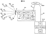
図15にセンサノードを3枚の基板で構成した例を示している。センサノードは、本体基板BO1、電源基板BO2および制御ソフト書き込み基板BO3から構成される。通常使用時には、本体基板BO1と電源基板BO2の組み合わせで使用される。また、制御ソフトウェアの書き換え時等には、本体基板BO1と制御ソフト書き込み基板BO3の組み合わせにて使用される。このうち、本体基板BO1の構成は、既に説明したセンサノードSN1と同様であるので、詳細な説明は省略する。 FIG. 15 shows an example in which the sensor node is composed of three substrates. The sensor node includes a main body board BO1, a power supply board BO2, and a control software writing board BO3. During normal use, the main board BO1 and the power supply board BO2 are used in combination. Further, when the control software is rewritten, it is used in a combination of the main body board BO1 and the control software writing board BO3. Among these, the configuration of the main body board BO1 is the same as that of the sensor node SN1 already described, and thus detailed description thereof is omitted.
電源基板BO2は、本体基板BO1との接続コネクタCN2、外付けセンサを接続する専用センサポートSP1、センサポートSP1の電源遮断を行う電源遮断スイッチPS21、パワーオンリセット回路POR1、手動リセットスイッチSW2、外部電源コネクタPP1、電源選択スイッチSW1、ボタン電池BAT1、レギュレータREG1から構成される。本基板BO2は、コネクタCN2経由で内蔵するボタン電池からの電力を本体基板BO1に供給する。また、センサポートSP1には、CN2経由で本体基板BO1からセンサを読み出すための信号線が配線されており、外付けのセンサを接続可能である。 The power supply board BO2 includes a connector CN2 connected to the main board BO1, a dedicated sensor port SP1 for connecting an external sensor, a power cutoff switch PS21 for shutting off the power of the sensor port SP1, a power-on reset circuit POR1, a manual reset switch SW2, an external It comprises a power connector PP1, a power selection switch SW1, a button battery BAT1, and a regulator REG1. The board BO2 supplies power from the button battery built in via the connector CN2 to the main board BO1. The sensor port SP1 is wired with a signal line for reading the sensor from the main board BO1 via CN2, and an external sensor can be connected.
制御ソフト書き込み基板BO3は、同様に、本体基板BO1との接続コネクタCN3、外付けセンサを接続する専用センサポートSP2、センサポートSP2の電源遮断を行う電源遮断スイッチPS21、パワーオンリセット回路POR2、手動リセットスイッチSW3、外部電源コネクタPP1、レギュレータREG2、および、プロセッサチップに搭載されるプログラム書き換えポートDBPから構成される。基板BO3は、外部電源コネクタPP1に接続された外部電源より電力を得て、本体基板BO1の動作に必要な電力の供給を行う。さらに、プログラム書き換え端子DBP経由で、本体基板BO1のプロセッサチップに搭載した制御ソフトウェアの書き換えを行う。このプログラム書き換え端子の信号線は、コネクタCN3、CN1経由で、プロセッサチップのプログラム書き換え端子に接続されており、この端子経由で搭載する制御ソフトウェアの書き換えを行う。 Similarly, the control software writing board BO3 includes a connector CN3 connected to the main board BO1, a dedicated sensor port SP2 for connecting an external sensor, a power cutoff switch PS21 for shutting off the power of the sensor port SP2, a power-on reset circuit POR2, and a manual operation. It comprises a reset switch SW3, an external power connector PP1, a regulator REG2, and a program rewrite port DBP mounted on the processor chip. The board BO3 obtains power from an external power source connected to the external power connector PP1, and supplies power necessary for the operation of the main board BO1. Furthermore, the control software mounted on the processor chip of the main board BO1 is rewritten via the program rewrite terminal DBP. The signal line of the program rewrite terminal is connected to the program rewrite terminal of the processor chip via the connectors CN3 and CN1, and rewrites the control software installed via this terminal.
以上のように、センサノードを別々の基板に分けて構成することには、以下のメリットがある。すなわち、通常使用時に不必要なプログラム書き換え端子を、本体基板BO1に搭載しなくてもすむ。このため、本体基板のサイズを小さくすることが可能となる。一方、ソフトウェアの動作確認/デバック時には、小さすぎるセンサノードは逆に扱いづらい。しかし、図15のような構成により、デバックに必要な信号線等は、サイズが問題にならない制御ソフト書き換え基板上に引き出すことも可能である。つまり、デバック作業にかかる手間を削減可能であり、開発にかかる期間を大幅に短縮可能である。 As described above, it is possible to divide and configure the sensor nodes on the separate substrates and have the following advantages. That is, it is not necessary to mount a program rewrite terminal unnecessary for normal use on the main body board BO1. For this reason, the size of the main body substrate can be reduced. On the other hand, at the time of software operation confirmation / debugging, a sensor node that is too small is difficult to handle. However, with the configuration as shown in FIG. 15, it is possible to draw out signal lines and the like necessary for debugging on a control software rewriting substrate whose size does not matter. That is, it is possible to reduce the time and effort required for the debugging work, and it is possible to greatly shorten the development period.
図16に示すのは、本発明のセンサノードを使用してセンサネットシステムを構築した例である。図16において、SN1〜SN6が本発明のセンサノードであり、例えば、建物全体の空調を制御する目的で、建物全体にばら撒かれる。これらばら撒かれたセンサノードは無線通信により、基地局BS1と無線通信を行い、センスした温度データを送信する。基地局BS1は、アンテナANT1、無線通信インタフェースRF1、プロセッサCPU1、メモリMEM1、二次記憶装置STR1、表示装置DISP1、ユーザーインタフェース装置UI1、及びネットワークインタフェースNI1から構成される。このうち、二次記憶装置STR1は、典型的には、ハードディスク等で構成される。また、表示装置DISP1はCRT等で、ユーザーインタフェース装置UI1は、キーボード/マウス等で構成される。図17に、本システムにてセンサノードから基地局に送信されるセンサデータのデータ構造を示す。基地局BS1は、無線インタフェース/アンテナ経由で、センサノードと無線通信を行い、温度等の測定データを読み出す。基地局BS1では、受信した測定データを元に、二次記憶装置STR1あるいはメモリMEM1上に格納されている品質判定プログラムQPR1に従って、建物全体の温度制御を行う。さらに、ネットワークインタフェースNI1経由で、インターネット等に代表される広域ネットワーク網WAN1を介して、遠隔地にある管理サーバーSV10と通信可能である。 FIG. 16 shows an example in which a sensor network system is constructed using the sensor node of the present invention. In FIG. 16, SN1 to SN6 are sensor nodes of the present invention, and are distributed over the entire building, for example, for the purpose of controlling the air conditioning of the entire building. These separated sensor nodes perform wireless communication with the base station BS1 by wireless communication and transmit sensed temperature data. The base station BS1 includes an antenna ANT1, a wireless communication interface RF1, a processor CPU1, a memory MEM1, a secondary storage device STR1, a display device DISP1, a user interface device UI1, and a network interface NI1. Of these, the secondary storage device STR1 is typically composed of a hard disk or the like. The display device DISP1 is a CRT or the like, and the user interface device UI1 is a keyboard / mouse or the like. FIG. 17 shows a data structure of sensor data transmitted from the sensor node to the base station in this system. The base station BS1 performs wireless communication with the sensor node via the wireless interface / antenna and reads measurement data such as temperature. The base station BS1 controls the temperature of the entire building according to the quality determination program QPR1 stored in the secondary storage device STR1 or the memory MEM1 based on the received measurement data. Furthermore, it is possible to communicate with the management server SV10 at a remote location via the network interface NI1 and the wide area network WAN1 represented by the Internet or the like.
本発明のセンサノードを使用することにより、まず、受信感度が良いため、遠くに基地局があっても確実に基地局との通信が可能となる。つまり、基地局の数を削減することができるため、センサネットシステムの導入にかかるコストを大幅に削減できる。さらに、本発明のセンサノードは電池寿命が長寿命であるため、頻繁に電池交換をしなくとも問題なく動作させ続けることが可能である。つまり、センサネットシステム全体でのメンテナンスコストを大幅に削減し、少ないコストで目的の機能を有するセンサネットシステムを構築することが可能となる。 By using the sensor node of the present invention, first, since the reception sensitivity is good, even if the base station is located far away, communication with the base station can be reliably performed. That is, since the number of base stations can be reduced, the cost for introducing the sensor network system can be greatly reduced. Furthermore, since the sensor node of the present invention has a long battery life, it can continue to operate without problems without frequent battery replacement. That is, it is possible to greatly reduce the maintenance cost of the entire sensor network system and to construct a sensor network system having a target function at a low cost.
本発明により高感度、低消費電力で動作可能なセンサノードが提供され、それにより種々の分野におけるセンサネットシステムの構築が可能になる。 According to the present invention, a sensor node capable of operating with high sensitivity and low power consumption is provided, which makes it possible to construct a sensor network system in various fields.
SN1 … センサノード、SIDE1 … 基板の第1の面、SIDE2 … 基板の第2の面、CA, CB, CC, CD … 基板の4つのコーナー、CHIP1, CHIP2 … 半導体集積回路、C1, C2, C3, C4 … コンデンサ、X1, X2, X3 … 水晶振動子あるいはセラミック振動子、ANT1 … アンテナ、LNA … 高周波低雑音増幅器、RFSW … 高周波スイッチ、MA … 高周波インピーダンスマッチング回路、RF … 高周波回路(データ変復調、PLL、VCOを含む)、OSC … 発振回路、CON … 制御回路、DISP … LED表示モニタ、CPU …プロセッサ回路、ADC … A/D変換回路、MEM, CMEM1 … メモリ、SIO … シリアル通信回路、TM1 … タイマ回路、PIO … プログラマブル入出力回路、LSC … RFSW/LNAの制御回路、PS1, PS2, PS11, PS21, PS22 … 電源遮断スイッチ、TS … 温度センサ、CN1, CN2, CN3 … コネクタ、VDD … 第1の電源ライン、VDD2 … 第2の電源ライン、VDD3 … 第3の電源ライン、GND … グランド電位、IF1 … インタフェース、V1, V2, V3, V4, V5, V6, V7, V10, V11, V13, V15, V21, V22, V23 … 基板の表面と裏面を接続するためのビア(貫通穴)、DS … データ信号線、CS … 制御信号線、DC … LED表示モニタの制御信号線、RES … CHIP2のリセット信号線、AP … A/D変換信号線、DP … デジタルI/O信号線、AT … 温度センサの出力信号線、VP1 … 基板内部に設けられた第1の電源層、GP1 … 基板内部に設けられたグランド層、VH10, VH11, VH13, VHI1, VH15 … ビアを通過させるためにGP1に設けられた領域、VH20, VH21, VH22, VH23, VHI1 … ビアを通過させるためにVP1に設けられた領域、MP1 … P型MOSトランジスタ、BP1 … PNP型バイポーラトランジスタ、MN1 … N型MOSトランジスタ、BN1 … NPN型バイポーラトランジスタ、IV10, IV20, IV21 … インバータ、R1, R2, R3, R4, R10 … 抵抗器、SDATA … センサからのデータを読み取った結果を格納したファイル、PDATA … 通信条件、タイマ起動間隔、センサノード毎に固有なID番号、デバイス毎の消費電流値に関する情報を格納したファイル、I0, I1, I2, I3, I4, I5, Ip0, Ip1, Ip2, Ip3 … 消費電流値、SP1 … 外部センサコネクタ、SEN1, SEN2 … 外部センサ、PP1 … 外部電源コネクタ、REG1 … 低電圧レギュレータ、POR … パワーオンリセット回路、BAT … 電池、SW1, SW2, SW3 … スイッチ、DBP … プログラム書き込み端子、VEX1 …外部電源ライン、BS …プログラム書き込み信号線、HDD1 … 二次記憶装置、DISP1 … 表示装置、NI1, NI10 … ネットワークインタフェース、DB10 … データベース、BA1 … ボタン電池。 SN1… Sensor node, SIDE1… First side of substrate, SIDE2… Second side of substrate, CA, CB, CC, CD… Four corners of substrate, CHIP1, CHIP2… Semiconductor integrated circuit, C1, C2, C3 , C4… Capacitor, X1, X2, X3… Crystal or ceramic resonator, ANT1… Antenna, LNA… High frequency low noise amplifier, RFSW… High frequency switch, MA… High frequency impedance matching circuit, RF… High frequency circuit (data modulation / demodulation, (Including PLL and VCO), OSC ... Oscillator, CON ... Control circuit, DISP ... LED display monitor, CPU ... Processor circuit, ADC ... A / D converter, MEM, CMEM1 ... Memory, SIO ... Serial communication circuit, TM1 ... Timer circuit, PIO… Programmable input / output circuit, LSC… RFSW / LNA control circuit, PS1, PS2, PS11, PS21, PS22… Power supply cutoff switch, TS… Temperature sensor, CN1, CN2, CN3… Connector, VDD… First Power line, V DD2… 2nd power line, VDD3… 3rd power line, GND… Ground potential, IF1… Interface, V1, V2, V3, V4, V5, V6, V7, V10, V11, V13, V15, V21, V22 , V23 ... Via (through hole) for connecting the front and back of the board, DS ... Data signal line, CS ... Control signal line, DC ... Control signal line for LED display monitor, RES ... Reset signal line for CHIP2, AP ... A / D conversion signal line, DP ... Digital I / O signal line, AT ... Temperature sensor output signal line, VP1 ... First power layer provided inside the substrate, GP1 ... Ground layer provided inside the substrate , VH10, VH11, VH13, VHI1, VH15 ... Area provided in GP1 for passing vias, VH20, VH21, VH22, VH23, VHI1 ... Area provided in VP1 for passing vias, MP1 ... P Type MOS transistor, BP1 ... PNP type bipolar transistor, MN1 ... N type MOS transistor, BN1 ... NPN type transistor Ipolar transistor, IV10, IV20, IV21… Inverter, R1, R2, R3, R4, R10… Resistor, SDATA… A file that stores the data read from the sensor, PDATA… Communication condition, timer start interval, sensor ID number unique to each node, file that stores information on current consumption for each device, I0, I1, I2, I3, I4, I5, Ip0, Ip1, Ip2, Ip3… current consumption, SP1… external sensor connector , SEN1, SEN2… External sensor, PP1… External power connector, REG1… Low voltage regulator, POR… Power-on reset circuit, BAT… Battery, SW1, SW2, SW3… Switch, DBP… Program write pin, VEX1… External power supply line , BS ... Program write signal line, HDD1 ... Secondary storage device, DISP1 ... Display device, NI1, NI10 ... Network interface, DB10 ... Database, BA1 ... Button battery.
Claims (7)
上記コネクタを経由して上記センサからセンサデータの入力を受け、上記センサデータから送信データを形成する第1の信号処理回路と、
上記第1の信号処理回路からの上記送信データを高周波信号に変換する第2の信号処理回路と、
上記高周波信号の入力を受け、アンテナを介して出力する入出力回路と、
上記コネクタ及び上記第1の信号処理回路を実装する第1の面と、上記第2の信号処理回路及び上記入出力回路を実装する第2の面とを有する基板と、を有し、
上記第1の信号処理回路と上記第2の信号処理回路との間の信号経路が折り返すように上記第1の面と上記第2の面が上記基板の表裏をなす電子装置。 And a connector for connecting the sensor,
A first signal processing circuit for receiving sensor data input from the sensor via the connector and forming transmission data from the sensor data ;
A second signal processing circuit for converting the transmission data from the first signal processing circuit into a high-frequency signal ;
An input / output circuit that receives the high-frequency signal and outputs it via an antenna;
A board having a first surface on which the connector and the first signal processing circuit are mounted, and a second surface on which the second signal processing circuit and the input / output circuit are mounted ;
An electronic device in which the first surface and the second surface make the front and back of the substrate so that a signal path between the first signal processing circuit and the second signal processing circuit is folded back .
上記基板には、上記第1の信号処理回路から発生するノイズを上記第2の信号処理回路
に伝達するのを抑制するシールド層を設けた電子装置。 In claim 1,
An electronic device in which the substrate is provided with a shield layer that suppresses transmission of noise generated from the first signal processing circuit to the second signal processing circuit.
上記シールド層として、第1電位が与えられる第1のプレーン層と第2電位が与えられ
る第2のプレーン層が設けられ、
上記第1電位は上記第1の信号処理回路の基準電位であり、上記第2電位は上記第1の
信号処理回路の電源電位である電子装置。 In claim 2,
As the shield layer, a first plane layer to which a first potential is applied and a second plane layer to which a second potential is applied are provided,
The electronic device, wherein the first potential is a reference potential of the first signal processing circuit, and the second potential is a power supply potential of the first signal processing circuit.
上記第1のプレーン層は、上記第2のプレーン層よりも上記基板の第2の面に近い層と
して形成された電子装置。 In claim 3,
The electronic device, wherein the first plane layer is formed as a layer closer to the second surface of the substrate than the second plane layer.
上記シールド層が、上記基板の内部に設置されている電子装置。An electronic device in which the shield layer is installed inside the substrate.
上記センサは上記コネクタを介して電源を供給され、The sensor is supplied with power through the connector,
上記第1の信号処理回路は、上記センサを間欠的に動作させ、上記センサを動作させないときには上記センサへの電源供給を遮断する電子装置。The first signal processing circuit is an electronic device that operates the sensor intermittently and shuts off power supply to the sensor when the sensor is not operated.
上記電子装置に内蔵された内蔵センサを有し、Having a built-in sensor built in the electronic device,
上記第1の信号処理回路は、上記内蔵センサを間欠的に動作させ、上記内蔵センサを動作させないときには上記内蔵センサへの電源供給を遮断する電子装置。The first signal processing circuit is an electronic device that intermittently operates the built-in sensor and cuts off power supply to the built-in sensor when the built-in sensor is not operated.
Priority Applications (5)
| Application Number | Priority Date | Filing Date | Title |
|---|---|---|---|
| JP2004064973A JP4049112B2 (en) | 2004-03-09 | 2004-03-09 | Electronic equipment |
| CN2008100876640A CN101257768B (en) | 2004-03-09 | 2004-09-01 | Electronic circuit and its control method |
| CNB2004100749810A CN100533997C (en) | 2004-03-09 | 2004-09-01 | Electronic circuit and control method therefor |
| US10/933,270 US7304857B2 (en) | 2004-03-09 | 2004-09-03 | Sensor node and circuit board arrangement |
| US11/976,041 US7663893B2 (en) | 2004-03-09 | 2007-10-19 | Sensor node and circuit board arrangement |
Applications Claiming Priority (1)
| Application Number | Priority Date | Filing Date | Title |
|---|---|---|---|
| JP2004064973A JP4049112B2 (en) | 2004-03-09 | 2004-03-09 | Electronic equipment |
Related Child Applications (1)
| Application Number | Title | Priority Date | Filing Date |
|---|---|---|---|
| JP2006139687A Division JP4301254B2 (en) | 2006-05-19 | 2006-05-19 | Electronic device and sensor network system |
Publications (3)
| Publication Number | Publication Date |
|---|---|
| JP2005260291A JP2005260291A (en) | 2005-09-22 |
| JP2005260291A5 JP2005260291A5 (en) | 2006-07-06 |
| JP4049112B2 true JP4049112B2 (en) | 2008-02-20 |
Family
ID=34918211
Family Applications (1)
| Application Number | Title | Priority Date | Filing Date |
|---|---|---|---|
| JP2004064973A Expired - Fee Related JP4049112B2 (en) | 2004-03-09 | 2004-03-09 | Electronic equipment |
Country Status (3)
| Country | Link |
|---|---|
| US (2) | US7304857B2 (en) |
| JP (1) | JP4049112B2 (en) |
| CN (2) | CN100533997C (en) |
Families Citing this family (25)
| Publication number | Priority date | Publication date | Assignee | Title |
|---|---|---|---|---|
| DE102004008738A1 (en) * | 2004-02-23 | 2005-09-08 | BSH Bosch und Siemens Hausgeräte GmbH | Electronic assembly and method of making this |
| JP4552670B2 (en) * | 2005-01-31 | 2010-09-29 | 株式会社日立製作所 | Sensor node, base station, and sensor network system |
| JP4848732B2 (en) * | 2005-10-17 | 2011-12-28 | 株式会社日立製作所 | Terminal device |
| US8290747B2 (en) * | 2005-10-21 | 2012-10-16 | Microstrain, Inc. | Structural damage detection and analysis system |
| JP4800981B2 (en) * | 2006-02-08 | 2011-10-26 | セイコーインスツル株式会社 | Wireless communication device |
| JP5285842B2 (en) * | 2006-04-13 | 2013-09-11 | パナソニック株式会社 | Integrated circuit mounting board and power line communication device |
| US8118483B2 (en) | 2006-06-21 | 2012-02-21 | Intel Corporation | Thermal sensor having toggle control |
| JP4814018B2 (en) | 2006-08-29 | 2011-11-09 | 株式会社日立製作所 | Sensor node |
| US20080225445A1 (en) * | 2007-03-14 | 2008-09-18 | Zippy Technology Corp. | Arc-discharge protection device with temperature detection mode |
| US8115629B2 (en) * | 2009-09-24 | 2012-02-14 | Microdata Corporation | Collective objects management system using R.F. object identification with multiple crystals |
| KR101049477B1 (en) | 2009-09-30 | 2011-07-15 | 제주대학교 산학협력단 | Sensor interface board assembly |
| JP5470556B2 (en) * | 2010-07-16 | 2014-04-16 | 伊原電子工業株式会社 | Biological signal detection device, control method thereof, and program |
| JP5269864B2 (en) * | 2010-12-07 | 2013-08-21 | 株式会社東芝 | Semiconductor device |
| US8971378B2 (en) | 2011-02-10 | 2015-03-03 | Mediatek Inc. | Wireless communication device |
| US9369172B2 (en) | 2011-02-10 | 2016-06-14 | Mediatek Inc. | Wireless communication device |
| US9258030B2 (en) | 2011-02-10 | 2016-02-09 | Mediatek Inc. | Wireless communication device |
| US9713093B2 (en) | 2011-02-10 | 2017-07-18 | Mediatek Inc. | Wireless communication device |
| JP5818310B2 (en) * | 2011-06-27 | 2015-11-18 | セイコーインスツル株式会社 | Sensor terminal, sensor system and method thereof |
| US20130039230A1 (en) * | 2011-08-09 | 2013-02-14 | Jaesik Lee | Method and Device for Wireless Broadcast Power-up Sequence in Wireless Sensor Network |
| WO2014016867A1 (en) * | 2012-07-24 | 2014-01-30 | ルネサスモバイル株式会社 | Semiconductor device and electronic apparatus |
| JP6340285B2 (en) | 2014-08-22 | 2018-06-06 | ルネサスエレクトロニクス株式会社 | Semiconductor device, electronic device and sensing method |
| JP6571358B2 (en) * | 2015-03-24 | 2019-09-04 | 三菱重工サーマルシステムズ株式会社 | Circuit board for power conversion and electric compressor |
| KR20160120496A (en) * | 2015-04-08 | 2016-10-18 | 삼성전기주식회사 | Mounting module |
| CN110402546B (en) * | 2017-03-15 | 2021-06-04 | 株式会社村田制作所 | High-frequency module and communication device |
| US11375607B2 (en) * | 2019-03-28 | 2022-06-28 | Apple Inc. | Mirrored voltage regulator for high-current applications and method the same |
Family Cites Families (30)
| Publication number | Priority date | Publication date | Assignee | Title |
|---|---|---|---|---|
| US4517535A (en) * | 1982-07-28 | 1985-05-14 | Dalmo Victor Operations, Bell Aerospace Textron, Div. Of Textron, Inc. | High speed high power step attenuator method and apparatus |
| US4616655A (en) * | 1984-01-20 | 1986-10-14 | Cordis Corporation | Implantable pulse generator having a single printed circuit board and a chip carrier |
| US5144548A (en) * | 1988-07-15 | 1992-09-01 | Iris Technologies, Inc. | Routing switcher |
| US5535274A (en) * | 1991-10-19 | 1996-07-09 | Cellport Labs, Inc. | Universal connection for cellular telephone interface |
| JPH1027987A (en) * | 1996-07-10 | 1998-01-27 | Hitachi Ltd | Low emi circuit board and low emi cable connector |
| US5938956A (en) * | 1996-09-10 | 1999-08-17 | Micron Technology, Inc. | Circuit and method for heating an adhesive to package or rework a semiconductor die |
| US5781078A (en) * | 1996-12-05 | 1998-07-14 | Glenayre Electronics, Inc. | Filter enhancement using input-to-output ground isolation and shielding |
| KR100238408B1 (en) * | 1997-02-26 | 2000-01-15 | 김승찬 | Anti-theft system for computer |
| US6010257A (en) * | 1997-03-18 | 2000-01-04 | Comtec Information Systems Inc. | Miniature portable interactive printer |
| US6064116A (en) * | 1997-06-06 | 2000-05-16 | Micron Technology, Inc. | Device for electrically or thermally coupling to the backsides of integrated circuit dice in chip-on-board applications |
| JPH117596A (en) | 1997-06-18 | 1999-01-12 | Penta Ocean Constr Co Ltd | Data detecting device and its power source managing method |
| AU9480798A (en) * | 1997-09-12 | 1999-03-29 | Williams Wireless, Inc. | Wide area remote telemetry |
| US6013876A (en) * | 1998-01-23 | 2000-01-11 | General Instrument Corporation | Method and device for electrically connecting circuits to opposite surfaces of a printed circuit board |
| JP3199039B2 (en) * | 1998-11-02 | 2001-08-13 | 日本電気株式会社 | Power consumption reduction circuit, wireless communication device using the same, and power consumption reduction method in wireless communication device |
| JP2001127652A (en) | 1999-10-22 | 2001-05-11 | Matsushita Electric Ind Co Ltd | High frequency radio |
| JP2001213008A (en) | 2000-02-03 | 2001-08-07 | Casio Comput Co Ltd | Gray scale print controller |
| JP2001232843A (en) | 2000-02-23 | 2001-08-28 | Alps Electric Co Ltd | Thermal printer and method of recording therefor |
| JP2001337931A (en) | 2000-05-29 | 2001-12-07 | Matsushita Electric Ind Co Ltd | Portable terminal device |
| US6487082B1 (en) * | 2000-07-20 | 2002-11-26 | Silicon Graphics, Inc. | Printed circuit board component packaging |
| JP4338885B2 (en) | 2000-08-22 | 2009-10-07 | パナソニック株式会社 | Mobile terminal device having wireless communication function and response method thereof |
| US6567703B1 (en) * | 2000-11-08 | 2003-05-20 | Medtronic, Inc. | Implantable medical device incorporating miniaturized circuit module |
| JP3642029B2 (en) | 2001-02-06 | 2005-04-27 | 日本電気株式会社 | Mobile phone |
| JP4274453B2 (en) | 2001-07-02 | 2009-06-10 | 横浜ゴム株式会社 | Vehicle tire monitoring system |
| US6672174B2 (en) * | 2001-07-23 | 2004-01-06 | Fidelica Microsystems, Inc. | Fingerprint image capture device with a passive sensor array |
| JP2003078279A (en) * | 2001-09-04 | 2003-03-14 | Konica Corp | Shielding method of printed board and device mounting printed board using that method |
| US8004854B2 (en) * | 2002-01-24 | 2011-08-23 | Adc Dsl Systems, Inc. | Electrical noise protection |
| JP2003234657A (en) | 2002-02-08 | 2003-08-22 | Sanyo Electric Co Ltd | Radio equipment |
| JP3980933B2 (en) * | 2002-05-23 | 2007-09-26 | ローム株式会社 | Manufacturing method of image sensor module |
| US6924496B2 (en) * | 2002-05-31 | 2005-08-02 | Fujitsu Limited | Fingerprint sensor and interconnect |
| US6903910B1 (en) * | 2004-08-06 | 2005-06-07 | Azijuth Networks, Inc. | Shielded enclosure with user-installable interface modules |
-
2004
- 2004-03-09 JP JP2004064973A patent/JP4049112B2/en not_active Expired - Fee Related
- 2004-09-01 CN CNB2004100749810A patent/CN100533997C/en not_active Expired - Fee Related
- 2004-09-01 CN CN2008100876640A patent/CN101257768B/en not_active Expired - Fee Related
- 2004-09-03 US US10/933,270 patent/US7304857B2/en not_active Expired - Fee Related
-
2007
- 2007-10-19 US US11/976,041 patent/US7663893B2/en not_active Expired - Fee Related
Also Published As
| Publication number | Publication date |
|---|---|
| CN100533997C (en) | 2009-08-26 |
| US7304857B2 (en) | 2007-12-04 |
| US7663893B2 (en) | 2010-02-16 |
| CN101257768B (en) | 2012-02-22 |
| JP2005260291A (en) | 2005-09-22 |
| US20080130253A1 (en) | 2008-06-05 |
| CN1667975A (en) | 2005-09-14 |
| US20050200002A1 (en) | 2005-09-15 |
| CN101257768A (en) | 2008-09-03 |
Similar Documents
| Publication | Publication Date | Title |
|---|---|---|
| JP4049112B2 (en) | Electronic equipment | |
| JP4301254B2 (en) | Electronic device and sensor network system | |
| JP4552670B2 (en) | Sensor node, base station, and sensor network system | |
| EP1626508B1 (en) | Transmission output control circuit, and wireless device using the same | |
| JP2011172206A (en) | High-frequency power amplifier and wireless communication device including the same | |
| US5546055A (en) | Crystal oscillator bias stabilizer | |
| JP2007074039A (en) | Power amplifying circuit, bias control method of power amplifying circuit, bias control program of power amplifying circuit, and storage medium | |
| JP2009153208A (en) | Electronic circuit and control method thereof | |
| JP4333809B2 (en) | Electronic circuit and control method thereof | |
| US6310517B1 (en) | Microwave amplifier | |
| US20110306311A1 (en) | Adaptively powered local oscillator generator circuit and related method | |
| US20190123437A1 (en) | Tunable slot resonator etched at the edge of a printed circuit board | |
| JP2009278616A (en) | Voltage controlled oscillator, and pll circuit, and radio communication device each including the same | |
| JP2006279201A (en) | Radio tag reader | |
| US10348253B2 (en) | Radio frequency module and communication device | |
| JP2003188653A (en) | Electronic components for radio communication and semiconductor integrated circuit for communication | |
| JP2006073821A (en) | Semiconductor integrated circuit device | |
| JP2000284836A (en) | Regulated power supply circuit | |
| JP2007028459A (en) | Amplifier circuit for radio transmission, radio transmitting/receiving circuit, semiconductor integrated circuit, and radio communication equipment | |
| JP2006134963A (en) | Receiving device and testing device | |
| KR20080006414A (en) | Front end module and communication system | |
| JP2005217753A (en) | Amplifier | |
| EP1897235A2 (en) | Oscillator coupling to reduce spurious signals in receiver circuits | |
| JP2006025233A (en) | Microwave amplifier circuit | |
| US20120082074A1 (en) | Radio communication device |
Legal Events
| Date | Code | Title | Description |
|---|---|---|---|
| RD04 | Notification of resignation of power of attorney |
Free format text: JAPANESE INTERMEDIATE CODE: A7424 Effective date: 20060424 |
|
| A521 | Written amendment |
Free format text: JAPANESE INTERMEDIATE CODE: A523 Effective date: 20060519 |
|
| A621 | Written request for application examination |
Free format text: JAPANESE INTERMEDIATE CODE: A621 Effective date: 20060519 |
|
| A977 | Report on retrieval |
Free format text: JAPANESE INTERMEDIATE CODE: A971007 Effective date: 20070629 |
|
| A131 | Notification of reasons for refusal |
Free format text: JAPANESE INTERMEDIATE CODE: A131 Effective date: 20070807 |
|
| A521 | Written amendment |
Free format text: JAPANESE INTERMEDIATE CODE: A523 Effective date: 20071009 |
|
| TRDD | Decision of grant or rejection written | ||
| A01 | Written decision to grant a patent or to grant a registration (utility model) |
Free format text: JAPANESE INTERMEDIATE CODE: A01 Effective date: 20071106 |
|
| A61 | First payment of annual fees (during grant procedure) |
Free format text: JAPANESE INTERMEDIATE CODE: A61 Effective date: 20071119 |
|
| FPAY | Renewal fee payment (event date is renewal date of database) |
Free format text: PAYMENT UNTIL: 20101207 Year of fee payment: 3 |
|
| FPAY | Renewal fee payment (event date is renewal date of database) |
Free format text: PAYMENT UNTIL: 20101207 Year of fee payment: 3 |
|
| FPAY | Renewal fee payment (event date is renewal date of database) |
Free format text: PAYMENT UNTIL: 20111207 Year of fee payment: 4 |
|
| FPAY | Renewal fee payment (event date is renewal date of database) |
Free format text: PAYMENT UNTIL: 20111207 Year of fee payment: 4 |
|
| FPAY | Renewal fee payment (event date is renewal date of database) |
Free format text: PAYMENT UNTIL: 20121207 Year of fee payment: 5 |
|
| LAPS | Cancellation because of no payment of annual fees |