JP4043335B2 - Receiver - Google Patents
Receiver Download PDFInfo
- Publication number
- JP4043335B2 JP4043335B2 JP2002295242A JP2002295242A JP4043335B2 JP 4043335 B2 JP4043335 B2 JP 4043335B2 JP 2002295242 A JP2002295242 A JP 2002295242A JP 2002295242 A JP2002295242 A JP 2002295242A JP 4043335 B2 JP4043335 B2 JP 4043335B2
- Authority
- JP
- Japan
- Prior art keywords
- correlation
- signal
- carrier
- receiving apparatus
- delay
- Prior art date
- Legal status (The legal status is an assumption and is not a legal conclusion. Google has not performed a legal analysis and makes no representation as to the accuracy of the status listed.)
- Expired - Fee Related
Links
Images


Classifications
-
- H—ELECTRICITY
- H04—ELECTRIC COMMUNICATION TECHNIQUE
- H04L—TRANSMISSION OF DIGITAL INFORMATION, e.g. TELEGRAPHIC COMMUNICATION
- H04L27/00—Modulated-carrier systems
- H04L27/26—Systems using multi-frequency codes
- H04L27/2601—Multicarrier modulation systems
- H04L27/2647—Arrangements specific to the receiver only
- H04L27/2655—Synchronisation arrangements
- H04L27/2662—Symbol synchronisation
-
- H—ELECTRICITY
- H04—ELECTRIC COMMUNICATION TECHNIQUE
- H04L—TRANSMISSION OF DIGITAL INFORMATION, e.g. TELEGRAPHIC COMMUNICATION
- H04L27/00—Modulated-carrier systems
- H04L27/26—Systems using multi-frequency codes
- H04L27/2601—Multicarrier modulation systems
- H04L27/2647—Arrangements specific to the receiver only
- H04L27/2655—Synchronisation arrangements
- H04L27/2668—Details of algorithms
- H04L27/2673—Details of algorithms characterised by synchronisation parameters
- H04L27/2675—Pilot or known symbols
Landscapes
- Engineering & Computer Science (AREA)
- Computer Networks & Wireless Communication (AREA)
- Signal Processing (AREA)
- Synchronisation In Digital Transmission Systems (AREA)
- Digital Transmission Methods That Use Modulated Carrier Waves (AREA)
Description
【0001】
【発明の属する技術分野】
本発明は、パイロットキャリアの挿入された直交周波数分割多重(Orthogonal Frequency Division Multiplex:OFDM)変調方式で変調された信号を受信する受信装置に係わり、ガードインターバルの相関性を利用したクロック同期処理あるいは遅延プロファイル生成処理を有するOFDM受信装置に関する。
【0002】
【従来の技術】
近年、移動体向けディジタル音声放送や、地上系ディジタルテレビジョン放送への応用に適した変調方式として、マルチパスフェージングやゴーストに強いという特徴のある、直交周波数分割多重変調(OFDM)方式が注目を浴びている。このOFDM方式は、マルチキャリア変調方式の一種であって、互いに直交するn本(nは数十〜数百)の搬送波(以下キャリアという)にディジタル変調を施した伝送方式である。
これらの各キャリアのI軸成分、Q軸成分には、各々に被変調信号として離散的な符号を割り当て、シンボル周期(数十μsec)毎にその符号を更新する。そして、図2に示すように、これらの多数のディジタル変調波を加算し、I軸、Q軸を直交変調して得られた変調信号を送信する。上記マルチキャリアのディジタル変調方式としては、4相差動位相偏移変調方式(DQPSK:Differential Quadrature Phase Shift Keying)も用いられているが、16値直交振幅変調方式(16QAM:16 Quadrature Amplitude Modulation)や32QAMなどの多値変調方式が良く用いられている。
【0003】
OFDM信号は、これら複数のキャリア対して逆フーリエ変換処理(IFFT)し、時間波形に変換する。 OFDM信号のシンボル構成は図3に示すように、IFFT処理後の時間軸波形である有効シンボルと、有効シンボルの一部を複写し、有効シンボルの前に付加したガードインターバルから構成される。OFDM方式は、ガードインターバルを付加することにより、ガードインターバル期間内の遅延時間の遅延波に対しては、そのシンボル間干渉による劣化を避けることが出来るため、マルチパスフェージングに対して強い耐性を有することができる。このように、ガードインターバルとしてシンボルの前半部分と後半部分で同一の信号を伝送しているため、OFDM伝送装置では、それらの相互相関性を復調や同期処理に利用している。
【0004】
次に、そのガードインターバルの相関性を利用した、本発明に係わる二点の処理について説明する。
第一点目として、OFDM方式は、サブキャリア間の周波数間隔が狭いため、送受信装置間のキャリア周波数誤差や復調系のサンプリングクロック周波数誤差によるサブキャリア間の干渉が生じ易く、それらの周波数の再生には高い精度が要求される。 つまり、OFDM信号を正しく受信し続けるためには、サンプリングクロック周波数を、送信信号のサンプリングクロック周波数に常に高精度に一致させ続けるというサンプリングクロック再生処理の必要がある。
そこで、ガードインターバルの相関性を利用してサンプリングクロック再生を行うものがある。(例えば、特許文献1参照)。 このOFDM伝送装置について、図16により簡単に説明する。
【0005】
受信アンテナ1に入力された受信信号は、高周波部2、中間周波数部3を経由し、ベースバンド信号に変換される。 このベースバンド信号は、A/D変換器4により、アナログ信号からディジタル信号に変換され、受信サンプリング系列(R)となり、FFT演算部8により、送信側でIFFT演算された時間波形信号が周波数波形信号に再生され、復調部9で元の信号に復調される。
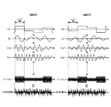
ここで、相関器13にて受信サンプリング系列(R)と有効シンボル遅延器11で有効シンボル期間長分遅延した信号との相互相関演算処理を行う。 そして、該相関結果から、ガードインターバル期間分の信号を抽出し、それらを加算処理する。この処理をサンプリングクロック毎に1サンプルづつずらしながら行う。ガードインターバル期間外では、双方の信号に相関性が無いため相関結果は0に近い値となるが、ガードインターバルに差し掛かると相関性を有し始め、そこから比例的に値が増加し、加算期間がちょうどガードインターバルと一致した時点で相関値はピーク値となる。そして、その時点が過ぎると、ガードインターバル期間とずれるため、相関値は減少し始める。 従って、この相関波形は、図4に示すように三角波となるが、実際には後述の様に、OFDM信号自体のランダム性により、雑音が加算されたような波形となる。
この相関値のピーク位置は、ガードインターバルの終了時点を指し示すため、ピーク位置を検出するシンボルタイミング検出部5において、このピーク位置が一定になるように、VCO制御部6を介し、VCO7のサンプリングクロック周波数を制御することで、クロック再生処理を実現することが出来る。
【0006】
第二点目として、OFDM伝送はその方式上、移動体伝送に用いられることが多い。屋外での伝送はその地形に応じて、送信機から直接到来する主波の他に、建物等から反射して遅延時間を伴って到来する反射波が存在するマルチパス通信路が形成される。更に、移動体伝送においては、主波と反射波のレベルも時々刻々と変化するフェージング環境も発生することがある。このようなマルチパスによって受信側のFFT復調窓が反射波に同期してしまったり、ガードインターバルを越えるような反射波が存在するとシンボル間干渉が発生してしまう。
このシンボル間干渉はC/N(キャリア対雑音比:Carrier/Noise)の劣化として現れ、符号誤り率が劣化してしまう。 従って、伝送の信頼性を上げるためには、ガードインターバルを越えるような反射波が存在しないような伝搬路環境を選んで伝送する必要がある。 このため、伝搬路特性を観測し、伝搬路特性に基づいた伝送を行うことは非常に信頼性の向上に有効な手段となる。
【0007】
伝搬路特性を観測する手段として最も良く用いられている方法に、主波や反射波のレベルと遅延時間を算出する遅延プロファイルがある。(例えば、特許文献2参照)。 この遅延プロファイルを算出するため、図16の相関器13で受信サンプリング信号と有効シンボル期間長分遅延した信号との相互相関処理を行い、相関結果をシンボル方向に平均処理することにより、図5に示すような波形を得ることが出来る。
この相関値の平均結果に対して、図16の微分器10で微分処理を行うことにより、図6の(a)に示すような微分波形を算出することが出来、微分波形に対して、負の信号成分を取り除くことにより、図6の(b)に示すような遅延プロファイル波形を得ることが出来る。
【0008】
【特許文献1】
特開平07−099486号公報
【特許文献2】
特開2002−232389公報
【0009】
【発明が解決しようとする課題】
前述のように、OFDM方式では各キャリアに16QAMや32QAMなどのディジタル変調を施すことがある。 これらの変調方式は、情報符号に対して、キャリア信号を図7に示すような信号点配置に構成し、各キャリアの振幅および位相に情報を持たせている。そのため、復調するためには、受信キャリアの絶対振幅、及び絶対位相を正確に再生する必要がある。
移動体伝送や、マルチパス環境下の様な劣悪な環境下では、各キャリアの振幅や位相が時々刻々と変化してしまうため、振幅、位相の再生は逐次、高速に行う必要がある。 そのため、振幅と位相が一定であるパイロットキャリアを数キャリア毎に配置して、パイロットキャリアに基づいて伝送路特性を推定し、振幅、位相の再生を行う方式が用いられている。 また、伝送性能を向上させるため、パイロットキャリアの振幅は通常のデータキャリアよりも大きめに設定することが多い。例えば、データキャリアと比較して、4/3倍の振幅比に設定する。
【0010】
パイロットキャリアの配置については、システム条件により異なり、その配置についての一例を、図8を用いて説明する。
図8の(a)はパイロットキャリアを8キャリア間隔、シンボル毎に配置している。このパイロットキャリアは、シンボル方向に連続して配置されているため、CP(Continuous Carrier)キャリアと称している。
図8の(b)はパイロットキャリアを8キャリア間隔に配置し、シンボル毎にキャリア位置をずらしているため、このパイロットキャリアをSP(Scattering Carrier)キャリアと称している。
ここで、等化可能なマルチパスの遅延時間は配置するキャリア間隔に依存し、等化可能なフェージング速度は配置するシンボル間隔に依存する。 また、伝送性能の向上のため、CPとSPを組み合わせて利用する方式もある。
しかし、これらのパイロットキャリアは、各シンボルで所定の繰り返し周期を持つ信号となるため、前述の従来技術で示したガードインターバル相関を取った場合、ガード期間だけでなく、シンボルの全期間にわたって相関性を有し、従来技術で説明した相関結果に影響を与えてしまう。
【0011】
具体例について、以下に、8キャリアサンプル毎に配置されたCPキャリアを用いたOFDM信号の例を用いて説明する。
第一の従来例で示した相関波形(図4)は、実際には、上記の様にCPキャリアのシンボル全期間にわたる相関性により、波形のフロア(信号の底辺部分)が上昇してしまう。図9は、これらのガードインターバル相関波形の比較について説明した図である。点線は図4で示したCPが存在しない場合のガードインターバル相関波形であり、実線はCPを挿入した場合の相関波形である。
このフロア上昇率は、8キャリア間隔でCPが挿入されている場合には、ピーク値の1/8にまで増加し、さらにCPの振幅が4/3と通常のデータキャリアよりも大きい場合には、ピーク値の0.22倍にフロアが位置してしまうことがある。
【0012】
この様に相関波形のフロアが上昇してしまうと、ピーク位置の検出結果に誤差が発生してしまう可能性が高くなる。 伝送路では、少なからず雑音が混入するので、確率的には本来のガードインターバル相関ピーク値よりも大きい値が生ずる可能性がある。 そのため、フロアが上昇した状態では、少ない雑音であってもピーク位置を誤検出し、サンプリングクロックの制御に悪影響を及ぼしてしまう可能性が高くなるという欠点が挙げられる。
また、受信信号に対して上記ピーク位置に基づいてFFT復調窓を設ける場合に、ピーク位置を誤検出し易いため、シンボル間干渉が生じてしまうという欠点も発生する。
【0013】
第二の従来例では、上記で説明した様に、CPキャリアは異なったシンボルであっても、シンボルの全期間にわたって相関性を有するため、マルチパスが混入すると図10に示すように、主波あるいは反射波同士のCPがそれぞれ相関性を有し、更に、主波と反射波のCPの相関性も絡み合って複雑な相関波形を生成してしまう。
その結果、図11に示す遅延プロファイルにも波形の乱れが生じ、レベルの小さい反射波は観測不能になってしまうという欠点も挙げられる。
【0014】
本発明はこれらの欠点を除去し、パイロットキャリアが挿入された場合のガードインターバルの相関演算を行う際、パイロットキャリアの相関成分による悪影響を除去し、データキャリアの相関性のみを抽出することで、ガードインターバルの相関演算を用いた同期処理、あるいは遅延プロファイルの生成等の性能向上を図ることを目的とする。
【0015】
【課題を解決するための手段】
本発明は上記目的を達成するため、複数のキャリアを用いて情報符号を伝送するマルチキャリア変調方式であって、該変調信号に振幅、位相が固定的であるパイロットキャリアが定期的に挿入されている信号を受信する受信装置において、受信信号と該受信信号を所定シンボル期間長あるいは上記パイロットキャリアの繰り返し周期に相当する期間長遅延させた信号との相互相関を演算する相関演算手段を有し、当該相関演算結果から上記パイロットキャリアにおける相関成分を抽出するようにしたものである。
また、ガードインターバルを有するOFDM方式であって、該変調信号に振幅、位相が固定的であるパイロットキャリアが定期的に挿入されている信号を受信する受信装置において、受信信号と該受信信号を所定シンボル期間長あるいはガードインターバル期間長遅延させた信号との相互相関を演算する相関演算手段と、上記受信信号あるいは上記所定シンボル期間長遅延させた受信信号と当該受信信号に対し相対的に有効シンボル期間長ずらした信号との相互相関を演算する相関演算手段と、上記後者の相関演算結果から上記前者の相関結果を減算する手段を有する受信装置である。
また、減算結果に基づき当該受信装置の受信サンプリングクロック周波数を送信側のクロック周波数に同期させるよう制御する手段を有する受信装置である。また、減算結果に基づき当該受信装置のFFT演算の時間窓位置を制御する手段を有する受信装置である。
また、減算結果に基づき遅延プロファイルを生成する手段を有する受信装置である。
【0016】
【発明の実施の形態】
以下、本発明によるOFDM伝送装置について、図1に図示する実施形態により詳細に説明する。
受信アンテナ1に入力された受信信号は、高周波部2、中間周波数部3を経由し、ベースバンド信号に変換される。 このベースバンド信号は、A/D変換器4により、アナログ信号からディジタル信号に変換され、受信サンプリング系列(R)となる。
受信サンプリング系列(R)は、有効シンボル遅延器11とNシンボル遅延器12に入力され、サンプリングクロック単位で所定の期間、遅延される。
有効シンボル遅延器11は、OFDMシンボルの有効シンボル期間長分の遅延を行い、Nシンボル遅延器12は、例えば1シンボル分の遅延を行う。 Nシンボル遅延器12での遅延量はシステムによって異なるが、具体例については後述する。
受信サンプリング系列(R)と、有効シンボル遅延器11の出力信号(VD)は、相関器13に入力される。 相関器13は、信号(R)と信号(VR)の相互相関演算を行い、それぞれの信号の相関性を算出する。
また、受信サンプリング系列(R)とNシンボル遅延器12の出力信号(SD)は相関器14に入力される。 相関器14は相関器13と同様の構成であり、信号(R)と信号(SD)の相関性を算出する。
【0017】
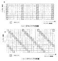
次に、これらガードインターバル相関演算の様子について、図12を用いて、詳細に説明する。 上段の矩形は受信サンプリング系列(R)を示し、中段は有効シンボル遅延器11の出力信号(VD)を、下段はNシンボル遅延器12の出力信号(SD)を、示している。
太い実線で囲まれた領域はOFDM信号の1シンボルを表し、その前半と後半の端部に網かけしてあるが、前半端部はガードインターバル、後半端部はガードインターバルと同一の信号成分を有している部分を表している。
ここで図12の中央部分の太い点線内の信号に着目して説明する。 ここで、信号(R)のドットで網かけされた部分と信号(VD)のドットで網かけされた部分は、同じシンボルの後半端部と前半端部であり、雑音や歪みが存在しない限り、同一の信号成分である。
そのため、これらの信号を相関器13にて相関性を算出すると、高い相関性を得ることが出来る。 この相関成分は、データキャリアとCPキャリア、即ち、OFDM信号の全てのキャリアが同一の成分であるので、データキャリアとCPキャリアの相関性の合成となる。
【0018】
次に、相関器14では、信号(R)と信号(SD)の相関性を演算するが、これは信号(R)のドット網かけ部分と信号(SD)の斜線網かけ部分の相関演算である。この場合も、ドット網かけ部分と斜線網かけ部分の相関成分は、それぞれデータキャリアとCPキャリアの合成となるが、異なるシンボルであるために、データキャリアについては、相関性を有さない。
しかし、CPキャリアは、図8(a)で説明したように、振幅、位相が一定であるため、シンボルが異なっても、それらの相関成分には相関性が現れる。
このように、相関器13からはデータキャリアとCPキャリアの相関性の合成成分、相関器14からはCPキャリアの相関成分が出力される。
そこで、減算器15によって、データキャリアとCPキャリアの合成相関成分である相関器13の出力信号から、CPキャリアの相関成分である相関器14の出力信号を減算する。 この処理を行うことにより、データキャリアとCPキャリアの合成相関成分からCPキャリアの相関成分を除去し、データキャリアのみのガードインターバル相関成分を抽出することが出来る。
【0019】
従来例の第一点目の項で述べたガードインターバルの相関演算は、CPが挿入されると図9の実線で示したようにフロアが上昇してしまうが、このフロア成分はCPキャリア同士の相関成分であるので、上記のように、減算器15にてCPの相関成分を除去すれば、図9の点線で示したようにフロア成分が低減する。
これによって、相関波形のピーク位置を誤検出する可能性が軽減するといった効果が得られる。
従って、減算器15から得られる相関値信号は、相関波形の正しいピーク位置を示すものとなるため、シンボルタイミング検出部5において、このピーク位置が一定になるように、VCO制御部6を介し、VCO7のサンプリングクロック周波数を制御することで、正確なクロック再生処理を実現することが出来る。
また、シンボルタイミング検出部5において、この正しいピーク位置に基づいてFFT演算の時間窓位置を制御する制御信号を生成し、FFT演算部8への受信サンプリング系列(R)の取り込みタイミングを制御することにより、シンボル間干渉の生じない、正しいFFT演算処理を行うことができる。
【0020】
第二点目については、図10、図11に示す様に、ガードインターバルの相関及び遅延プロファイルにCPの相関成分が混入しているため、波形に乱れが生じているが、同様に減算器15においてCPの相関成分を除去すれば、図5、図6に示すように波形の乱れがなくなる。 すなわち、微分器10の出力は、CPが存在しない場合の遅延プロファイルと同様に、精度の良い遅延プロファイル波形を観測することが出来る。
【0021】
次に、上記でNシンボル遅延器12の遅延量について説明を割愛したが、以下に遅延量の具体例について説明する。
基本的にはNシンボルの遅延量はCPキャリアの相関性のみを抽出出来れば、どのような値であっても良い。つまり、遅延量を2シンボル期間長分としても、2シンボル前のCPキャリアの振幅、位相が同一であれば相関性を抽出出来る。一般的に、遅延量はNシンボル(Nは1以上の整数)とすれば良いが、移動体伝送等では伝搬路の状況が時々刻々と変化するので、Nシンボルの時間差があってもほぼ同一の伝搬路環境であることが条件として挙げられる。
【0022】
使用される周波数帯域が低い場合は、フェージング速度が低くなるため、Nの値が比較的大きくても伝搬路環境の変化は少ないが、周波数帯域が高くなると、フェージング速度も速くなるので、Nの値を小さくしたほうが良い。
Nの値が小さい方が遅延量も少なく、使用するメモリ容量も少なくなるため、一般的には、N=1として最も遅延が少なくなるように選定する。
また、挿入されるパイロットキャリアは図8で説明したように、CPキャリアの他に、SPキャリアが挿入されることがある。
SPキャリアが挿入されている場合には、Nシンボル遅延器12の遅延量は、SPキャリアの挿入間隔に設定すれば、SPキャリアの相関性を抽出することが出来る。
図8(b)の例で説明すると、このSPキャリアの挿入間隔は8シンボル間隔であるので、N=8(8シンボルの遅延)とすることにより、SPキャリア同士の相関性を得ることが出来る。
【0023】
次に、図1で説明した本発明による構成から、遅延に必要なメモリ容量を低減することが出来る構成について、図13を用いて説明する。 ここで、図13は遅延に必要なメモリ容量を削減した場合の構成について説明した図であり、図1の受信アンテナ1からA/D変換器4までの構成及びシンボルタイミング検出部5から微分器10までの構成を省略しており、図1の有効シンボル遅延器11をガードインターバル遅延器21に、Nシンボル遅延器12をシンボル遅延器22に置き換え、減算器15の+端子と−端子を入れ換えた構成である。
図13の入力信号には、図1と同様に受信サンプリング系列(R)が入力され、ガードインターバル遅延器21とシンボル遅延器22に入力される。 ガードインターバル遅延器21では、ガードインターバル期間長の遅延を、シンボル遅延器22では1シンボル期間長の遅延を施す。
【0024】
図12と同様に、これらガードインターバル相関演算の様子を、図14の太い点線内を中心にして説明する。
ここで、ガードインターバル遅延器21の出力信号(GD)の斜線網かけ部分と受信サンプリング系列(R)のドット網かけ部分に対して相関演算を行うと、異なるシンボルのため、相関器13ではCPのみの相関性が算出される。
また、ガードインターバル遅延器21の出力信号(GD)の斜線網かけ部分と、シンボル遅延器22の出力信号(SD’)の斜線網かけ部分の相関演算を行うと、同じシンボルであるため、相関器14ではデータキャリアとCPの合成相関性が算出される。
減算器15では、図1とは逆に、相関器14の出力信号であるデータキャリアとCPキャリアの合成相関性から、相関器13の出力信号であるCPキャリアの相関性を減算することにより、図1と同様の効果を得ることが出来る。
【0025】
次に、図1と図13の構成における、遅延に必要なメモリ容量の比較をする。ここでは、有効シンボル長を1024サンプル、ガードインターバル長を128サンプルを例にとって説明する。
図1の有効シンボル遅延器11では1024サンプル分の遅延が、Nシンボル遅延器12では1152サンプル分(1024+128)の遅延が必要となるため、合計2176サンプル分の遅延容量が必要となる。
それに対して、図13の構成では、ガードインターバル遅延器21では128サンプル分の遅延が、シンボル遅延器22では1152サンプル分の遅延が必要となり、合計1280サンプル分の遅延容量となり、約0.6倍のメモリ容量で実現出来ることになる。
【0026】
次に、図13の構成において、更にメモリ容量を削減した場合の構成について図15を用いて説明する。
図15は、図13の構成において、シンボル遅延器22を除去し、ガードインターバル遅延器21の出力を有効シンボル遅延器11の入力に接続し、有効シンボル遅延器11の出力を相関器14の入力に接続した構成である。
図13で説明した様に、シンボル遅延器22は、受信サンプリング系列(R)に対して1シンボル期間長の遅延を行う必要があるが、ガードインターバル遅延器21でガードインターバル期間長の遅延を行っているので、その出力信号を有効シンボル遅延器11において有効シンボル期間長の遅延を行うことで、合計して1シンボル期間長の遅延を行うことが出来る。
図15の構成における必要メモリ容量は、ガードインターバル遅延器21での128サンプル分の遅延と、有効シンボル遅延器11での1024サンプル分の遅延となり、合計1152サンプル分の遅延となる。 これは、図1の構成に対して、約0.5倍のメモリ容量で実現出来ることになる。
【0027】
【発明の効果】
以上説明したように、本発明により、パイロットキャリアが挿入された場合のガードインターバルの相関演算を行う際、パイロットキャリアの相関成分による悪影響を除去し、データキャリアの相関性のみを抽出することで、ガードインターバルの相関演算を用いた同期処理、あるいは遅延プロファイルの生成等の性能を向上させることが出来る。
【図面の簡単な説明】
【図1】本発明のOFDM受信装置における同期再生、遅延プロファイル生成処理構成の一実施例を示すブロック図
【図2】OFDM信号の信号構成を示す波形図
【図3】OFDM信号のシンボル構成を示す波形図
【図4】ガードインターバル相関波形(サンプル方向積分)を示す波形図
【図5】ガードインターバル相関波形(シンボル方向平均)を示す波形図
【図6】遅延プロファイル波形を示す波形図
【図7】16QAMの信号点配置を示す模式図
【図8】パイロットキャリアの配置を示す模式図
【図9】CPが挿入された場合のガードインターバル相関波形を示す図
【図10】CPが挿入された場合のガードインターバル相関波形を示す図
【図11】CPが挿入された場合の遅延プロファイル波形を示す図
【図12】本発明の有効シンボル遅延器11とNシンボル遅延器12の動作を説明する図
【図13】本発明の他の実施例を示すブロック図
【図14】本発明のガードインターバル遅延器21とシンボル遅延器の動作を説明する図
【図15】本発明の他の実施例を示すブロック図
【図16】従来のOFDM受信装置における同期再生、遅延プロファイル生成処理構成の一例を示すブロック図
【符号の説明】
11:有効シンボル遅延器、12:Nシンボル遅延器、13,14:相関器、15:減算器、21:ガードインターバル遅延器、22:シンボル遅延器。[0001]
BACKGROUND OF THE INVENTION
The present invention relates to a receiving apparatus that receives a signal modulated by an Orthogonal Frequency Division Multiplex (OFDM) modulation system in which a pilot carrier is inserted, and relates to a clock synchronization process or delay using the correlation of guard intervals. The present invention relates to an OFDM receiver having a profile generation process.
[0002]
[Prior art]
In recent years, orthogonal frequency division multiplexing (OFDM), which is characterized by its resistance to multipath fading and ghosting, has attracted attention as a modulation method suitable for digital audio broadcasting for mobiles and terrestrial digital television broadcasting. I'm bathing. This OFDM system is a type of multi-carrier modulation system, and is a transmission system in which n (n is several tens to several hundreds) carrier waves (hereinafter referred to as carriers) orthogonal to each other are digitally modulated.
A discrete code is assigned to each of the I-axis component and Q-axis component of each carrier as a modulated signal, and the code is updated every symbol period (several tens of microseconds). Then, as shown in FIG. 2, a large number of these digital modulation waves are added, and a modulated signal obtained by orthogonally modulating the I axis and the Q axis is transmitted. As the multicarrier digital modulation method, a four-phase differential phase shift keying (DQPSK) method is also used, but a 16-value quadrature amplitude modulation method (16QAM) or 32QAM is used. Multi-level modulation schemes such as are often used.
[0003]
The OFDM signal is subjected to inverse Fourier transform processing (IFFT) for the plurality of carriers and converted into a time waveform. As shown in FIG. 3, the symbol structure of the OFDM signal includes an effective symbol that is a time-axis waveform after IFFT processing, and a guard interval that is obtained by copying a part of the effective symbol and adding it before the effective symbol. The OFDM system has a strong tolerance against multipath fading by adding a guard interval so that a delay wave having a delay time within the guard interval period can avoid deterioration due to intersymbol interference. be able to. As described above, since the same signal is transmitted as the guard interval in the first half and the second half of the symbol, the OFDM transmission apparatus uses their cross-correlation for demodulation and synchronization processing.
[0004]
Next, two points of processing according to the present invention using the correlation of the guard intervals will be described.
First, since the frequency interval between subcarriers is narrow in the OFDM system, interference between subcarriers is likely to occur due to a carrier frequency error between transmission / reception devices and a sampling clock frequency error in the demodulation system. Requires high accuracy. In other words, in order to continue to receive the OFDM signal correctly, it is necessary to perform a sampling clock regeneration process in which the sampling clock frequency is always matched with the sampling clock frequency of the transmission signal with high accuracy.
Therefore, there is one that performs sampling clock recovery using the correlation of guard intervals. (For example, refer to Patent Document 1). This OFDM transmission apparatus will be briefly described with reference to FIG.
[0005]
The received signal input to the
Here, the
Since the peak position of this correlation value indicates the end point of the guard interval, the sampling timing of the VCO 7 is passed through the
[0006]
Second, OFDM transmission is often used for mobile transmission because of its method. In the case of outdoor transmission, a multipath communication path is formed in which reflected waves that are reflected from a building or the like and arrive with a delay time exist in addition to the main wave that directly arrives from the transmitter. Furthermore, in mobile transmission, a fading environment may occur in which the levels of the main wave and the reflected wave change from moment to moment. If the FFT demodulation window on the receiving side is synchronized with the reflected wave due to such multipath, or if there is a reflected wave exceeding the guard interval, intersymbol interference occurs.
This intersymbol interference appears as degradation of C / N (Carrier / Noise), and the code error rate is degraded. Therefore, in order to improve the transmission reliability, it is necessary to select and transmit a propagation path environment in which no reflected wave exceeding the guard interval exists. For this reason, observing the propagation path characteristics and performing transmission based on the propagation path characteristics is a very effective means for improving the reliability.
[0007]
As a method most often used as means for observing propagation path characteristics, there is a delay profile for calculating the level and delay time of the main wave and reflected wave. (For example, refer to Patent Document 2). In order to calculate this delay profile, the
A differential waveform as shown in (a) of FIG. 6 can be calculated by performing a differentiation process on the average result of the correlation values by the
[0008]
[Patent Document 1]
Japanese Patent Laid-Open No. 07-099486 [Patent Document 2]
JP 2002-232389 A
[Problems to be solved by the invention]
As described above, in the OFDM system, each carrier may be subjected to digital modulation such as 16QAM or 32QAM. In these modulation schemes, carrier signals are arranged in a signal point arrangement as shown in FIG. 7 for information codes, and information is given to the amplitude and phase of each carrier. Therefore, in order to demodulate, it is necessary to accurately reproduce the absolute amplitude and absolute phase of the received carrier.
In an inferior environment such as mobile transmission or in a multipath environment, the amplitude and phase of each carrier change from moment to moment. Therefore, it is necessary to reproduce the amplitude and phase sequentially and at high speed. For this reason, a method is used in which pilot carriers having constant amplitude and phase are arranged every several carriers, transmission path characteristics are estimated based on the pilot carriers, and amplitude and phase are reproduced. In order to improve transmission performance, the amplitude of the pilot carrier is often set larger than that of a normal data carrier. For example, the amplitude ratio is set to 4/3 times that of the data carrier.
[0010]
The arrangement of pilot carriers varies depending on the system conditions, and an example of the arrangement will be described with reference to FIG.
In FIG. 8A, pilot carriers are arranged at intervals of 8 carriers for each symbol. Since this pilot carrier is continuously arranged in the symbol direction, it is called a CP (Continuous Carrier) carrier.
In FIG. 8B, pilot carriers are arranged at intervals of 8 carriers, and the carrier positions are shifted for each symbol, so this pilot carrier is called an SP (Scattering Carrier) carrier.
Here, the multipath delay time that can be equalized depends on the arranged carrier interval, and the fading speed that can be equalized depends on the arranged symbol interval. There is also a method of using a combination of CP and SP in order to improve transmission performance.
However, since these pilot carriers are signals having a predetermined repetition period in each symbol, when the guard interval correlation shown in the above-mentioned prior art is taken, the correlation is not limited to the entire period of the symbol, not only the guard period. Which affects the correlation result described in the prior art.
[0011]
A specific example will be described below using an example of an OFDM signal using a CP carrier arranged every 8 carrier samples.
In the correlation waveform (FIG. 4) shown in the first conventional example, the waveform floor (the bottom portion of the signal) actually rises due to the correlation over the entire CP carrier symbol period as described above. FIG. 9 is a diagram illustrating comparison of these guard interval correlation waveforms. A dotted line is a guard interval correlation waveform when the CP shown in FIG. 4 does not exist, and a solid line is a correlation waveform when a CP is inserted.
This floor increase rate increases to 1/8 of the peak value when CPs are inserted at intervals of 8 carriers, and when the CP amplitude is 4/3, which is larger than a normal data carrier. The floor may be located 0.22 times the peak value.
[0012]
If the floor of the correlation waveform rises in this way, there is a high possibility that an error will occur in the peak position detection result. Since not a little noise is mixed in the transmission line, there is a possibility that a value larger than the original guard interval correlation peak value may occur stochastically. Therefore, when the floor is raised, there is a disadvantage that the peak position is erroneously detected even if there is little noise, and the possibility of adversely affecting the control of the sampling clock is increased.
In addition, when an FFT demodulation window is provided on the received signal based on the peak position, the peak position is easily detected erroneously, which causes a drawback that intersymbol interference occurs.
[0013]
In the second conventional example, as described above, even if the CP carrier is a different symbol, it has a correlation over the entire period of the symbol. Alternatively, the CPs of the reflected waves have a correlation, and the correlation between the CPs of the main wave and the reflected wave is also entangled to generate a complex correlation waveform.
As a result, the waveform of the delay profile shown in FIG. 11 is also disturbed, and a reflected wave having a low level cannot be observed.
[0014]
The present invention eliminates these disadvantages, and when performing the correlation calculation of the guard interval when the pilot carrier is inserted, by removing the adverse effect due to the correlation component of the pilot carrier and extracting only the correlation of the data carrier, It is an object to improve performance such as synchronization processing using guard interval correlation calculation or delay profile generation.
[0015]
[Means for Solving the Problems]
In order to achieve the above object, the present invention is a multi-carrier modulation system for transmitting an information code using a plurality of carriers, in which a pilot carrier having a fixed amplitude and phase is periodically inserted into the modulation signal. A receiving apparatus that receives a received signal and a correlation calculating means for calculating a cross-correlation between the received signal and a signal obtained by delaying the received signal by a predetermined symbol period length or a period length corresponding to the repetition period of the pilot carrier, A correlation component in the pilot carrier is extracted from the correlation calculation result.
Further, in a receiving apparatus that receives a signal that is a OFDM system having a guard interval and in which a pilot carrier whose amplitude and phase are fixed is periodically inserted in the modulated signal, the received signal and the received signal are predetermined. Correlation calculating means for calculating a cross-correlation with a signal delayed by a symbol period length or a guard interval period length, and an effective symbol period relative to the received signal or the received signal delayed by the predetermined symbol period length and the received signal It is a receiving device having correlation calculating means for calculating a cross-correlation with a signal shifted by a long distance and means for subtracting the former correlation result from the latter correlation calculation result.
Further, the receiving apparatus includes means for controlling the receiving sampling clock frequency of the receiving apparatus to be synchronized with the clock frequency on the transmitting side based on the subtraction result. Further, the receiving apparatus has means for controlling the time window position of the FFT operation of the receiving apparatus based on the subtraction result.
Further, the receiving apparatus includes means for generating a delay profile based on the subtraction result.
[0016]
DETAILED DESCRIPTION OF THE INVENTION
Hereinafter, an OFDM transmission apparatus according to the present invention will be described in detail with reference to an embodiment shown in FIG.
The received signal input to the receiving
The received sampling sequence (R) is input to the effective
The effective
The received sampling sequence (R) and the output signal (VD) of the effective
The received sampling sequence (R) and the output signal (SD) of the N
[0017]
Next, the state of the guard interval correlation calculation will be described in detail with reference to FIG. The upper rectangle shows the received sampling sequence (R), the middle row shows the output signal (VD) of the effective
A region surrounded by a thick solid line represents one symbol of the OFDM signal, and the first half and the latter half thereof are shaded, but the first half end is the guard interval, and the second half end has the same signal component as the guard interval. The part which has is represented.
Here, the description will be made by paying attention to the signal within the thick dotted line in the central portion of FIG. Here, the portion shaded by the dot of the signal (R) and the portion shaded by the dot of the signal (VD) are the second half and the first half of the same symbol, as long as there is no noise or distortion. Are the same signal components.
Therefore, high correlation can be obtained by calculating correlation between these signals by the
[0018]
Next, the
However, since the CP carrier has a constant amplitude and phase as described with reference to FIG. 8A, even if the symbols are different, a correlation appears in their correlation components.
Thus, the
Therefore, the
[0019]
In the correlation calculation of the guard interval described in the first item of the conventional example, when the CP is inserted, the floor rises as shown by the solid line in FIG. Since it is a correlation component, if the CP correlation component is removed by the
As a result, an effect of reducing the possibility of erroneously detecting the peak position of the correlation waveform is obtained.
Accordingly, since the correlation value signal obtained from the
Further, the symbol
[0020]
As for the second point, as shown in FIGS. 10 and 11, since the correlation component of the CP is mixed in the correlation and delay profile of the guard interval, the waveform is disturbed. If the correlation component of CP is removed in FIG. 5, the waveform disturbance is eliminated as shown in FIGS. That is, the output of the
[0021]
Next, description of the delay amount of the N
Basically, the delay amount of N symbols may be any value as long as only the correlation of the CP carrier can be extracted. That is, even if the delay amount is equal to the length of two symbol periods, the correlation can be extracted if the amplitude and phase of the CP carrier two symbols before are the same. In general, the delay amount may be N symbols (N is an integer equal to or greater than 1). However, in mobile transmission or the like, the state of the propagation path changes from moment to moment, so even if there is a time difference of N symbols, it is almost the same. As a condition, it is necessary to be a propagation path environment.
[0022]
When the frequency band to be used is low, the fading speed is low, so even if the value of N is relatively large, the change in the propagation path environment is small. However, if the frequency band is high, the fading speed is also high. It is better to reduce the value.
The smaller the value of N, the smaller the amount of delay and the smaller the memory capacity to be used. In general, N = 1 is selected so that the delay is minimized.
In addition, as described with reference to FIG. 8, an SP carrier may be inserted in addition to a CP carrier as a pilot carrier to be inserted.
When the SP carrier is inserted, the correlation of the SP carrier can be extracted by setting the delay amount of the N
In the example of FIG. 8B, since the SP carrier insertion interval is 8 symbol intervals, correlation between SP carriers can be obtained by setting N = 8 (8 symbol delay). .
[0023]
Next, a configuration capable of reducing the memory capacity required for delay from the configuration according to the present invention described in FIG. 1 will be described with reference to FIG. Here, FIG. 13 is a diagram for explaining the configuration when the memory capacity required for the delay is reduced. The configuration from the receiving
As in FIG. 1, the received sampling sequence (R) is input to the input signal of FIG. 13 and input to the guard
[0024]
Similar to FIG. 12, the state of the guard interval correlation calculation will be described with a focus on the thick dotted line in FIG.
Here, if the correlation calculation is performed on the hatched portion of the output signal (GD) of the guard
Further, if the correlation calculation is performed on the hatched portion of the output signal (GD) of the guard
In the
[0025]
Next, the memory capacity required for delay in the configurations of FIGS. 1 and 13 will be compared. Here, an explanation will be given taking an effective symbol length of 1024 samples and a guard interval length of 128 samples as an example.
The effective
On the other hand, in the configuration of FIG. 13, the guard
[0026]
Next, in the configuration of FIG. 13, a configuration when the memory capacity is further reduced will be described with reference to FIG.
FIG. 15 shows the configuration of FIG. 13, with the
As described with reference to FIG. 13, the
The required memory capacity in the configuration of FIG. 15 is a delay of 128 samples in the guard
[0027]
【The invention's effect】
As described above, according to the present invention, when performing the correlation calculation of the guard interval when the pilot carrier is inserted, the adverse effect due to the correlation component of the pilot carrier is removed, and only the correlation of the data carrier is extracted. It is possible to improve performance such as synchronization processing using guard interval correlation calculation or generation of a delay profile.
[Brief description of the drawings]
FIG. 1 is a block diagram showing an embodiment of a synchronous reproduction and delay profile generation processing configuration in an OFDM receiver of the present invention. FIG. 2 is a waveform diagram showing a signal configuration of an OFDM signal. Waveform diagram showing the guard interval correlation waveform (sample direction integration) Fig. 5 Waveform diagram showing the guard interval correlation waveform (symbol direction average) Fig. 6 Waveform diagram showing the delay profile waveform 7] Schematic diagram showing 16QAM signal point arrangement [Fig. 8] Schematic diagram showing pilot carrier arrangement [Fig. 9] Diagram showing guard interval correlation waveform when CP is inserted [Fig. 10] CP inserted FIG. 11 shows a delay profile waveform when a CP is inserted. FIG. 12 shows an effective symbol delay of the present invention. FIG. 13 is a block diagram illustrating another embodiment of the present invention. FIG. 14 illustrates operations of the guard
11: Effective symbol delay, 12: N symbol delay, 13, 14: Correlator, 15: Subtractor, 21: Guard interval delay, 22: Symbol delay
Claims (5)
Priority Applications (3)
| Application Number | Priority Date | Filing Date | Title |
|---|---|---|---|
| JP2002295242A JP4043335B2 (en) | 2002-10-08 | 2002-10-08 | Receiver |
| EP03022243.4A EP1408664B1 (en) | 2002-10-08 | 2003-10-01 | Reception of multicarrier signals |
| US10/679,337 US6774829B2 (en) | 2002-10-08 | 2003-10-07 | Apparatus and method for receiving signals including data carriers and pilot carriers modulated by multi-carrier modulation method |
Applications Claiming Priority (1)
| Application Number | Priority Date | Filing Date | Title |
|---|---|---|---|
| JP2002295242A JP4043335B2 (en) | 2002-10-08 | 2002-10-08 | Receiver |
Publications (2)
| Publication Number | Publication Date |
|---|---|
| JP2004134883A JP2004134883A (en) | 2004-04-30 |
| JP4043335B2 true JP4043335B2 (en) | 2008-02-06 |
Family
ID=32025517
Family Applications (1)
| Application Number | Title | Priority Date | Filing Date |
|---|---|---|---|
| JP2002295242A Expired - Fee Related JP4043335B2 (en) | 2002-10-08 | 2002-10-08 | Receiver |
Country Status (3)
| Country | Link |
|---|---|
| US (1) | US6774829B2 (en) |
| EP (1) | EP1408664B1 (en) |
| JP (1) | JP4043335B2 (en) |
Families Citing this family (31)
| Publication number | Priority date | Publication date | Assignee | Title |
|---|---|---|---|---|
| US6943712B1 (en) | 2003-11-06 | 2005-09-13 | Marvell International Ltd. | Voltage built-in real-time digital non-linearity measurement device and method for analog to digital converters |
| US7450669B2 (en) * | 2003-12-08 | 2008-11-11 | Panasonic Corporation | Demodulation apparatus and method, and integrated circuit of demodulation apparatus |
| US7339999B2 (en) | 2004-01-21 | 2008-03-04 | Qualcomm Incorporated | Pilot transmission and channel estimation for an OFDM system with excess delay spread |
| US8553822B2 (en) | 2004-01-28 | 2013-10-08 | Qualcomm Incorporated | Time filtering for excess delay mitigation in OFDM systems |
| WO2005086729A2 (en) * | 2004-03-05 | 2005-09-22 | Nextnet Wireless, Inc. | System and method for adaptive modulation |
| DE602004011899T2 (en) * | 2004-04-21 | 2009-02-12 | Sony Deutschland Gmbh | Frame synchronization with interference reduction |
| US7457231B2 (en) * | 2004-05-04 | 2008-11-25 | Qualcomm Incorporated | Staggered pilot transmission for channel estimation and time tracking |
| US20050265219A1 (en) * | 2004-05-11 | 2005-12-01 | Texas Instruments Incorporated | Orthogonal frequency division multiplex (OFDM) packet detect unit, method of detecting an OFDM packet and OFDM receiver employing the same |
| DE102004028806B3 (en) * | 2004-06-15 | 2005-12-29 | Infineon Technologies Ag | Receiver for a wireless communication system |
| US7596181B2 (en) | 2004-09-18 | 2009-09-29 | Samsung Electronics Co., Ltd. | Apparatus and method for frequency synchronization in OFDM system |
| CN100566317C (en) * | 2004-10-22 | 2009-12-02 | 财团法人工业技术研究院 | Coherent OFDM receiver method for synchronous and device based on frequency dependence |
| US7587016B2 (en) * | 2005-07-20 | 2009-09-08 | Broadcom Corporation | MIMO timing recovery |
| CN101305537B (en) * | 2005-11-10 | 2010-12-22 | 富士通株式会社 | Receiving apparatus, error-detecting circuit and receiving method |
| US20080069264A1 (en) * | 2006-09-14 | 2008-03-20 | Tomokazu Sada | Data transmitting apparatus and data receiving apparatus |
| JP4351279B2 (en) * | 2007-09-20 | 2009-10-28 | Okiセミコンダクタ株式会社 | OFDM demodulator |
| JP5021517B2 (en) * | 2008-02-18 | 2012-09-12 | 株式会社日立国際電気 | OFDM receiving apparatus and OFDM relay apparatus |
| US7944999B2 (en) * | 2008-04-04 | 2011-05-17 | Newport Media, Inc. | Robust fine frequency and time estimation in mobile multimedia multicast system receivers |
| JP5237860B2 (en) * | 2009-03-11 | 2013-07-17 | 日本放送協会 | Digital broadcast receiver |
| JP5293480B2 (en) * | 2009-07-27 | 2013-09-18 | 富士通株式会社 | Frequency control apparatus, frequency control method, base station apparatus, and mobile station apparatus |
| WO2011094001A1 (en) * | 2010-01-26 | 2011-08-04 | Sirius Xm Radio Inc. | Method of improving performance in a hierarchical modulation system |
| JP5678609B2 (en) * | 2010-11-26 | 2015-03-04 | セイコーエプソン株式会社 | Cross correlation determination method and cross correlation determination device |
| US8750176B2 (en) | 2010-12-22 | 2014-06-10 | Apple Inc. | Methods and apparatus for the intelligent association of control symbols |
| US9838226B2 (en) | 2012-01-27 | 2017-12-05 | Apple Inc. | Methods and apparatus for the intelligent scrambling of control symbols |
| US8897398B2 (en) * | 2012-01-27 | 2014-11-25 | Apple Inc. | Methods and apparatus for error rate estimation |
| US9450790B2 (en) | 2013-01-31 | 2016-09-20 | Apple Inc. | Methods and apparatus for enabling and disabling scrambling of control symbols |
| US9210010B2 (en) | 2013-03-15 | 2015-12-08 | Apple, Inc. | Methods and apparatus for scrambling symbols over multi-lane serial interfaces |
| JP5878266B2 (en) * | 2013-06-13 | 2016-03-08 | 株式会社日立国際電気 | Antenna direction adjusting method and OFDM receiving apparatus |
| TWI520494B (en) * | 2013-11-07 | 2016-02-01 | 晨星半導體股份有限公司 | Circuit for calculating error of sampling clock and method thereof, and signal receiving circuit and method thereof |
| US9520910B1 (en) * | 2015-09-24 | 2016-12-13 | Nxp B.V. | Receiver component and method for enhancing a detection range of a time-tracking process in a receiver |
| CN107306238B (en) * | 2016-04-21 | 2021-03-02 | 北京三星通信技术研究有限公司 | Method for receiving and transmitting carrier modulation signals, and corresponding receiver and transmitter |
| US10560254B1 (en) * | 2017-08-15 | 2020-02-11 | L3 Technologies Inc. | Picosecond LPD time alignment |
Family Cites Families (4)
| Publication number | Priority date | Publication date | Assignee | Title |
|---|---|---|---|---|
| JP3074103B2 (en) * | 1993-11-16 | 2000-08-07 | 株式会社東芝 | OFDM synchronous demodulation circuit |
| JPH10209998A (en) * | 1997-01-20 | 1998-08-07 | Sony Corp | Demodulation device |
| JP3797397B2 (en) | 1997-05-02 | 2006-07-19 | ソニー株式会社 | Receiving apparatus and receiving method |
| EP1063824B1 (en) * | 1999-06-22 | 2006-08-02 | Matsushita Electric Industrial Co., Ltd. | Symbol synchronisation in multicarrier receivers |
-
2002
- 2002-10-08 JP JP2002295242A patent/JP4043335B2/en not_active Expired - Fee Related
-
2003
- 2003-10-01 EP EP03022243.4A patent/EP1408664B1/en not_active Expired - Fee Related
- 2003-10-07 US US10/679,337 patent/US6774829B2/en not_active Expired - Fee Related
Also Published As
| Publication number | Publication date |
|---|---|
| JP2004134883A (en) | 2004-04-30 |
| US6774829B2 (en) | 2004-08-10 |
| EP1408664B1 (en) | 2013-12-11 |
| US20040071221A1 (en) | 2004-04-15 |
| EP1408664A2 (en) | 2004-04-14 |
| EP1408664A3 (en) | 2006-12-27 |
Similar Documents
| Publication | Publication Date | Title |
|---|---|---|
| JP4043335B2 (en) | Receiver | |
| EP1108295B1 (en) | Method for forming a training sequeence | |
| EP1746794B1 (en) | Path selection in an OFDM apparatus | |
| EP1624602B1 (en) | Demodulation device and demodulation method | |
| CN1846415B (en) | System and method for two channel frequency offset estimation of OFDM signals | |
| EP1207663B1 (en) | Signal quality assessment in a multicarrier receiver | |
| EP1349337B1 (en) | Multicarrier reception with interference detection | |
| US6720824B2 (en) | Demodulation method and apparatus | |
| JP3022854B1 (en) | Delay profile analyzer and symbol synchronization method | |
| KR19990043408A (en) | Method and apparatus for simple frequency acquisition of orthogonal split-band systems | |
| JP2002511711A (en) | Method and apparatus for fine frequency synchronization in a multi-carrier demodulation system | |
| US20080063040A1 (en) | Equalizer demodulating a signal including sp symbols and an equalization method therefor | |
| KR100347965B1 (en) | Coarse frequency synchronization in multicarrier systems | |
| KR100213100B1 (en) | Frequency error corrector for orthogonal frequency division multiplexing and method therefor | |
| KR100341200B1 (en) | Quadrature frequency division multiplexing demodulator | |
| EP2159981B1 (en) | OFDM signal receiving apparatus and receiving method | |
| US8229042B2 (en) | Orthogonal frequency division multiplexing demodulator | |
| JP5175761B2 (en) | OFDM receiver | |
| JP3768108B2 (en) | OFDM receiver | |
| JP4362955B2 (en) | Demodulator and demodulation method | |
| KR100391565B1 (en) | An Rayleigh Fading Compensation Method with Modified Sinc Interpolation | |
| Garcia et al. | Tracking of time misalignments for OFDM systems in multipath fading channels | |
| JP2000138647A (en) | Digital transmission system | |
| JP2003258759A (en) | Demodulation method for transmission signal, receiver, and signal transmission system | |
| JP2001069113A (en) | Multicarrier synchronous detecting circuit |
Legal Events
| Date | Code | Title | Description |
|---|---|---|---|
| A621 | Written request for application examination |
Free format text: JAPANESE INTERMEDIATE CODE: A621 Effective date: 20050915 |
|
| A977 | Report on retrieval |
Free format text: JAPANESE INTERMEDIATE CODE: A971007 Effective date: 20070912 |
|
| TRDD | Decision of grant or rejection written | ||
| A01 | Written decision to grant a patent or to grant a registration (utility model) |
Free format text: JAPANESE INTERMEDIATE CODE: A01 Effective date: 20071113 |
|
| A61 | First payment of annual fees (during grant procedure) |
Free format text: JAPANESE INTERMEDIATE CODE: A61 Effective date: 20071113 |
|
| R150 | Certificate of patent or registration of utility model |
Ref document number: 4043335 Country of ref document: JP Free format text: JAPANESE INTERMEDIATE CODE: R150 Free format text: JAPANESE INTERMEDIATE CODE: R150 |
|
| FPAY | Renewal fee payment (event date is renewal date of database) |
Free format text: PAYMENT UNTIL: 20101122 Year of fee payment: 3 |
|
| FPAY | Renewal fee payment (event date is renewal date of database) |
Free format text: PAYMENT UNTIL: 20111122 Year of fee payment: 4 |
|
| FPAY | Renewal fee payment (event date is renewal date of database) |
Free format text: PAYMENT UNTIL: 20111122 Year of fee payment: 4 |
|
| FPAY | Renewal fee payment (event date is renewal date of database) |
Free format text: PAYMENT UNTIL: 20121122 Year of fee payment: 5 |
|
| FPAY | Renewal fee payment (event date is renewal date of database) |
Free format text: PAYMENT UNTIL: 20121122 Year of fee payment: 5 |
|
| FPAY | Renewal fee payment (event date is renewal date of database) |
Free format text: PAYMENT UNTIL: 20131122 Year of fee payment: 6 |
|
| R250 | Receipt of annual fees |
Free format text: JAPANESE INTERMEDIATE CODE: R250 |
|
| R250 | Receipt of annual fees |
Free format text: JAPANESE INTERMEDIATE CODE: R250 |
|
| LAPS | Cancellation because of no payment of annual fees |