JP3797397B2 - Receiving apparatus and receiving method - Google Patents
Receiving apparatus and receiving method Download PDFInfo
- Publication number
- JP3797397B2 JP3797397B2 JP11471097A JP11471097A JP3797397B2 JP 3797397 B2 JP3797397 B2 JP 3797397B2 JP 11471097 A JP11471097 A JP 11471097A JP 11471097 A JP11471097 A JP 11471097A JP 3797397 B2 JP3797397 B2 JP 3797397B2
- Authority
- JP
- Japan
- Prior art keywords
- signal
- phase
- circuit
- clock signal
- frequency
- Prior art date
- Legal status (The legal status is an assumption and is not a legal conclusion. Google has not performed a legal analysis and makes no representation as to the accuracy of the status listed.)
- Expired - Fee Related
Links
Images


Classifications
-
- H—ELECTRICITY
- H04—ELECTRIC COMMUNICATION TECHNIQUE
- H04L—TRANSMISSION OF DIGITAL INFORMATION, e.g. TELEGRAPHIC COMMUNICATION
- H04L27/00—Modulated-carrier systems
- H04L27/26—Systems using multi-frequency codes
- H04L27/2601—Multicarrier modulation systems
- H04L27/2647—Arrangements specific to the receiver only
- H04L27/2655—Synchronisation arrangements
- H04L27/2657—Carrier synchronisation
-
- H—ELECTRICITY
- H04—ELECTRIC COMMUNICATION TECHNIQUE
- H04L—TRANSMISSION OF DIGITAL INFORMATION, e.g. TELEGRAPHIC COMMUNICATION
- H04L27/00—Modulated-carrier systems
- H04L27/26—Systems using multi-frequency codes
- H04L27/2601—Multicarrier modulation systems
- H04L27/2647—Arrangements specific to the receiver only
- H04L27/2655—Synchronisation arrangements
- H04L27/2662—Symbol synchronisation
-
- H—ELECTRICITY
- H04—ELECTRIC COMMUNICATION TECHNIQUE
- H04L—TRANSMISSION OF DIGITAL INFORMATION, e.g. TELEGRAPHIC COMMUNICATION
- H04L27/00—Modulated-carrier systems
- H04L27/26—Systems using multi-frequency codes
- H04L27/2601—Multicarrier modulation systems
- H04L27/2647—Arrangements specific to the receiver only
- H04L27/2655—Synchronisation arrangements
- H04L27/2668—Details of algorithms
- H04L27/2673—Details of algorithms characterised by synchronisation parameters
- H04L27/2676—Blind, i.e. without using known symbols
- H04L27/2679—Decision-aided
Landscapes
- Engineering & Computer Science (AREA)
- Computer Networks & Wireless Communication (AREA)
- Signal Processing (AREA)
- Synchronisation In Digital Transmission Systems (AREA)
Description
【0001】
【発明の属する技術分野】
本発明は、受信装置および受信方法に関し、特に、OFDM方式に基づく受信装置および受信方法に関する。
【0002】
【従来の技術】
近年デジタル信号を伝送する方法として、直交周波数分割多重方式(OFDM:Orthogonal Frequency Division Multiplexing)と呼ばれる変調方式が提案されている。このOFDM方式は伝送帯域内に多数の直交する副搬送波を設け、それぞれの副搬送波の振幅及び位相にデータを割り当て、PSK(Phase Shift Keying)やQAM(Quadrature Amplitude Modulation)によりディジタル変調する方式である。この方法では、多数の副搬送波で伝送帯域を分割するため、副搬送波1波あたりの帯域は狭くなり、変調速度は遅くなるが、搬送波の数が多数あるので総合の伝送速度は従来の変調方式と変わらない。
【0003】
このOFDM方式では多数の副搬送波が並列に伝送されるためにシンボル速度が遅くなるので、いわゆるマルチパス妨害の存在する伝送路ではシンボルの時間長に対する相対的なマルチパスの時間長を短くすることができ、マルチパス妨害に対して強い方式であることが期待できる。
【0004】
以上の様な特徴からOFDM方式は、マルチパス妨害の影響を強く受ける地上波によるディジタル信号の伝送に対して特に注目されている。このような地上波によるディジタル信号の伝送としては、例えば、DVB−T(Digital Video Broadcasting-Terrestrial)などが有名である。
【0005】
また最近の半導体技術の進歩により離散的フ−リエ変換(以下FFT(Fast Fourier Transform)と記述する)や離散的フ−リエ逆変換(以下IFFT(Invert Fast Fourier Transform)と記述する)をハ−ドウェアで実現することが可能となり、これらを用いて簡単にOFDM方式に基づく変調を行ったり、また逆に復調する事ができる様になった事もOFDM方式が注目されてきた理由の一つである。
【0006】
図10はOFDM受信機の構成例を示すブロック図である。受信アンテナ101は、RF信号を捕捉する。乗算回路102は、チューナ103から出力される所定の周波数を有する信号とRF信号とを乗算する。バンドパスフィルタ104は、乗算回路102の出力から所望のIF信号を抽出する。A/D(Anagolgue to Digital)変換回路105は、バンドパスフィルタ104により抽出されたIF信号をディジタル信号に変換する。
【0007】
デマルチプレクサ106は、ディジタル化されたIF信号からIチャンネル信号とQチャンネル信号とを分離抽出する。ローパスフィルタ107,108は、それぞれ、Iチャンネル信号とQチャンネル信号に含まれている不要な高域成分を除去して基底帯域(ベースバンド)の信号に変換する。
【0008】
複素乗算回路109は、数値コントロール発振回路110より供給される所定の周波数の信号により、基底帯域信号の持つ搬送波周波数誤差を除外した後、高速フーリエ変換回路112に供給する。高速フーリエ変換回路112はOFDM時間信号を周波数分解し、IおよびQチャンネル受信デ−タを生成する。
【0009】
相関値演算回路113は、基底帯域に変換されたOFDM時間信号と有効シンボル時間だけ遅延させたOFDM信号とを乗算してガード期間幅の移動平均を計算することにより、2つの信号の相関値を求め、相関値が最大になるタイミングにおいて高速フーリエ変換回路112に演算を開始させる。
【0010】
搬送波周波数誤差演算回路114は、周波数パワーの偏りを検出することにより搬送波周波数の誤差を算出し、加算回路111に出力する。加算回路111は、搬送波周波数誤差演算回路114と相関値演算回路113の出力を加算して数値コントロール発振回路110に供給する。
【0011】
クロック周波数再生回路115は、IチャンネルデータとQチャンネルデータを参照して制御信号を生成し、クロック発振回路116の発振周波数を制御する。クロック発振回路116は、クロック周波数再生回路115から供給される制御信号に応じてクロック信号を生成し、出力する。
【0012】
次に、以上の従来例の動作について説明する。
【0013】
受信アンテナ101により捕捉されたRF信号は、チューナ103より供給された所定の周波数の信号と乗算回路102により乗算される。乗算回路102より出力された信号は、バンドパスフィルタ104により、IF信号が抽出されることになる。
【0014】
A/D変換回路105は、クロック発振回路116が出力するクロック信号に同期して、バンドパスフィルタ104から出力されるIF信号をディジタル信号に変換し、デマルチプレクサ106に供給する。デマルチプレクサ106は、ディジタル化された信号からIチャンネル信号とQチャンネル信号とを分離抽出してローパスフィルタ107,108にそれぞれ供給する。ローパスフィルタ107,108は、それぞれ、Iチャンネル信号とQチャンネル信号に含まれている不要な高域成分である折り返し成分を除去して基底帯域の信号に変換する。
【0015】
複素乗算回路109は、数値コントロール発振回路110より供給される所定の周波数の信号により、基底帯域信号の持つ搬送波の周波数誤差を除去して高速フーリエ変換回路112に供給する。高速フーリエ変換回路112はOFDM時間信号を周波数分解し、IおよびQチャンネル受信デ−タを生成する。
【0016】
相関値演算回路113は、基底帯域に変換されたOFDM時間信号と有効シンボル時間だけ遅延させたOFDM信号との間の相関値を計算し、相関値が最大になるタイミングにおいて高速フーリエ変換回路112に演算を開始させる。その結果、高速フーリエ変換回路112は、送信側から送られてきたIチャンネル信号とQチャンネル信号に含まれているデータを正確に抽出することができる。
【0017】
ところで受信側において、OFDM信号を正しく復調する為には、各種の同期を取ることが必要となる。例えば、先ず、IF帯のOFDM信号を基底帯域のOFDM信号に変換するためには、数値コントロール発振回路110が発振する周波数を送信側のそれと同期させなければならない。また、全ての処理の基準となるクロック信号も送信側のそれと同期させなければならない。
【0018】
ここで、後者のクロック信号を送信側と同期させるための方法として、従来から提案されているクロックの再生方法について説明する。
【0019】
以下に述べる方法では、送信側においては伝送しようとする情報以外に、振幅および位相が規定された特定の信号(以下、パイロット信号という)が各シンボル毎に所定の数だけ内挿されて送信されており。また、受信側においては、FFT演算が施されたOFDM信号から送信側で内挿されたパイロット信号が抽出され、このパイロット信号に以下に述べるコスタス演算等を施すことによりクロック信号を再生する。
【0020】
図11は、パイロット信号がQPSK(Quadrature Phase Shift Keying)で変調されている場合に、コスタス演算を用いてクロック信号を再生する従来のクロック再生回路の構成例である。この図において、ゲート回路208−1,208−2は、FFT演算が施されたIチャンネルデータと、Qチャンネルデータをそれぞれ入力し、パイロット信号だけを抽出して出力する。2乗回路203−1,203−2は、ゲート回路208−1,208−2により抽出されたパイロット信号をそれぞれ2乗して出力する。乗算回路205は、ゲート回路208−1,208−2により抽出されたパイロット信号を乗算して出力する。
【0021】
減算回路206は、2乗回路203−1の出力から2乗回路203−2の出力を減算して出力する。乗算回路207は、乗算回路205の出力と減算回路206の出力を乗算して出力する。LPF209は、乗算回路207の出力から不要な高周波成分を除去して出力する。
【0022】
次に、以上の従来例の動作について説明する。
【0023】
図10に示す高速フーリエ変換回路112により周波数分解されて復調されたIチャンネルデータおよびQチャンネルデータは、その周波数が小さい順にゲート回路208−1,208−2にそれぞれ入力される。ゲート回路208−1,208−2は、IチャンネルデータおよびQチャンネルデータよりパイロット信号のみをそれぞれ抽出し、2乗回路203−1,203−2、および、乗算回路205に供給する。
【0024】
乗算回路205は、ゲート回路208−1,208−2により抽出されたパイロット信号を乗算して、乗算回路207に出力する。また、2乗回路203−1,203−2は、それぞれ、ゲート回路208−1,208−2により抽出されたパイロット信号を2乗して減算回路206に出力する。
【0025】
減算回路206は、2乗回路203−1の出力から2乗回路203−2の出力を減算して乗算回路207に出力する。乗算回路207は、乗算回路205の出力と減算回路207の出力を乗算してLPF209に出力する。LPF209は、乗算回路207の出力に含まれている高周波成分を除去して出力する。
【0026】
以上のような一連の操作がいわゆるコスタス演算であり、このようなコスタス演算により、クロック信号の位相誤差を検出することができる。このようにして検出されたクロック信号の位相誤差に基づいてクロック発振回路116を制御して正確なクロック信号を生成する。
【0027】
【発明が解決しようとする課題】
ところで、以上のようなコスタス演算等を用いて位相誤差を検出し、その結果に応じてクロック信号を再生する場合、検出された位相誤差には、クロック周波数誤差に伴う位相誤差だけではなく、再生搬送波位相誤差、FFT窓位相誤差、ガウス雑音による位相誤差、および、地上波を伝送する場合には避けて通れないマルチパスによる伝送路ひずみに起因する位相誤差が含まれているため、再生クロック誤差のみに伴う位相誤差だけを抽出してクロック発信回路を制御することが困難であるという課題があった。
【0028】
また、図12(A)にOFDM信号のスペクトラムの一例を、図12(B)にはマルチパス妨害を受けたときのOFDM信号のスペクトラムを示す。ここで太線は送信側で内挿されたパイロット信号を表している。図12(B)に示すように、マルチパスにより送信信号が周波数選択的な妨害を受けた場合、他の副搬送波に対するパイロット信号の信号対雑音比が低下する。そのような場合、前述のような方法によりパイロット信号から生成されたクロック信号の位相誤差信号も信号対雑音比が低下することになる。その結果、送信信号がマルチパス妨害を受けた場合には、正確にクロック信号を再生することが困難となるという問題があった。
【0029】
本発明は以上のような状況に鑑みてなされたものであり、受信したOFDM信号がクロック周波数誤差に伴う位相誤差のみならず、再生搬送波位相誤差、FFT窓位相誤差、ガウス雑音による位相誤差、および、マルチパスによる伝送路ひずみに起因する位相誤差を含む場合においても、クロック信号を正確に生成することができるOFDM受信装置のクロック再生回路を提供することを目的としている。
【0030】
【課題を解決するための手段】
請求項1に記載の受信装置は、OFDM信号を離散的フーリエ変換する変換手段と、変換手段により得られた副搬送波の周波数成分を記憶する記憶手段と、記憶手段に記憶されている少なくとも1シンボル前の周波数成分と、変換手段により新たに得られた周波数成分との間の位相変動量を算出する算出手段と、算出手段により算出された位相変動量より、パイロット信号に対応する成分を抽出する抽出手段と、受信装置において使用されるクロック信号を発生するクロック信号発生手段であって、クロック信号の周波数が制御可能なクロック信号発生手段と、抽出手段により抽出されたパイロット信号に対応する位相変動量を複数のパイロット信号にわたって累積加算し、この累積加算された信号に応じてクロック信号発生手段を制御してクロック信号の周波数を制御する制御手段とを備えることを特徴とする。
【0031】
請求項4に記載の受信方法は、受信装置が、受信装置において使用されるクロック信号を発生するクロック信号発生手段であって、クロック信号の周波数が制御可能なクロック信号発生手段を備えており、OFDM信号を離散的フーリエ変換する変換ステップと、変換ステップにより得られた副搬送波の周波数成分を記憶する記憶ステップと、記憶ステップに記憶されている少なくとも1シンボル前の周波数成分と、変換ステップにより新たに得られた周波数成分との間の位相変動量を算出する算出ステップと、算出ステップにより算出された位相変動量より、パイロット信号に対応する成分を抽出する抽出ステップと、抽出ステップにより抽出されたパイロット信号に対応する位相変動量を複数のパイロット信号にわたって累積加算し、この累積加算された信号に応じてクロック信号発生手段を制御してクロック信号の周波数を制御する制御ステップとを備えることを特徴とする。
【0034】
請求項1に記載の受信装置においては、OFDM信号を変換手段が離散的フーリエ変換し、変換手段により得られた副搬送波の周波数成分を記憶手段が記憶し、記憶手段に記憶されている少なくとも1シンボル前の周波数成分と、変換手段により新たに得られた周波数成分との間の位相変動量を算出手段が算出し、算出手段により算出された位相変動量より、パイロット信号に対応する成分を抽出手段が抽出し、クロック信号の周波数が制御可能なクロック信号発生手段が受信装置において使用されるクロック信号を発生し、抽出手段により抽出されたパイロット信号に対応する位相変動量を複数のパイロット信号にわたって累積加算し、この累積加算された信号に応じてクロック信号発生手段を制御してクロック信号の周波数を制御手段が制御する。例えば、変換手段であるFFT変換回路がOFDM信号を離散的フーリエ変換し、得られた副搬送波の周波数成分を記憶手段であるメモリが記憶し、メモリに記憶されている1シンボル前の周波数成分と、FFT変換回路より新たに出力された周波数成分とを算出手段が差動復調することにより位相変動量を算出し、算出手段により算出された位相変動量からパイロット信号に対応する成分を抽出手段が抽出し、クロック信号の周波数が制御可能なクロック信号発生手段が受信装置において使用されるクロック信号を発生し、抽出手段により抽出されたパイロット信号の位相変動量を複数のパイロット信号にわたって累積加算し、この累積加算された信号に応じてクロック信号発生手段を制御してクロック信号の周波数を制御手段が制御する。
【0035】
請求項4に記載の受信方法においては、受信装置が、受信装置において使用されるクロック信号を発生するクロック信号発生手段であって、クロック信号の周波数が制御可能なクロック信号発生手段を備えており、OFDM信号を変換ステップが離散的フーリエ変換し、変換ステップにより得られた副搬送波の周波数成分を記憶ステップが記憶し、記憶ステップに記憶されている少なくとも1シンボル前の周波数成分と、変換ステップにより新たに得られた周波数成分との間の位相変動量を算出ステップが算出し、算出ステップにより算出された位相変動量より、パイロット信号に対応する成分を抽出ステップが抽出し、抽出ステップにより抽出されたパイロット信号に対応する位相変動量を複数のパイロット信号にわたって累積加算し、この累積加算された信号に応じてクロック信号発生手段を制御してクロック信号の周波数を制御ステップが制御する。例えば、変換ステップであるFFT変換回路がOFDM信号を離散的フーリエ変換し、得られた副搬送波の周波数成分を記憶ステップであるメモリが記憶し、メモリに記憶されている1シンボル前の周波数成分と、FFT変換回路より新たに出力された周波数成分とを算出ステップが差動復調することにより位相変動量を算出し、算出ステップにより算出された位相変動量からパイロット信号に対応する成分を抽出ステップが抽出し、抽出ステップにより抽出されたパイロット信号の位相変動量を複数のパイロット信号にわたって累積加算し、この累積加算された信号に応じてクロック信号発生手段を制御してクロック信号の周波数を制御ステップが制御する。
【0038】
図1に本発明の実施の形態の一例を示す。なお、本実施の形態は図10に示すクロック周波数再生回路115に関するものである。
【0039】
この図において、差動復調回路503は、RAM(Random Access Memory)506,507、符号反転回路510、および、複素乗算回路511により構成されており、入力されたIチャンネルデータおよびQチャンネルデータを差動復調するようになされている。RAM506,507は、入力されたIチャンネルデータまたはQチャンネルデータを、制御回路520からの制御信号cに応じて、シンボル単位で記憶し、1シンボル時間だけ遅らせて出力するようになされている。符号反転回路510は、RAM507の出力データの符号を反転して出力するようになされている。
【0040】
複素乗算回路511は、遅延されていないIチャンネルデータとQチャンネルデータをI,Qと表し、遅延されたIチャンネルデータとQチャンネルデータをそれぞれI-1,Q-1と表すと、以下に示す複素演算を行い、演算結果を実数成分523と虚数成分524とに分けて出力するようになされている。なお、ここで、jは虚数を表す。
【0041】
(I+jQ)(I-1−jQ-1) ・・・(1)
【0042】
ROM(Read Only Memory)512は、アークタンジェント(逆正接関数)データを格納しており、入力されたIチャンネルデータおよびQチャンネルデータに対応する位相変動量データ513を出力するようになされている。
【0043】
ゲート回路514は、制御回路520の制御信号に従ってROM512から出力される位相変動量データ513から、送信側で規定されたパイロット信号に対応する成分だけを選択し、符号反転回路521およびセレクタ522に供給するようになされている。符号反転回路521は入力された位相変動量データの符号を反転し、セレクタ522に供給するようになされている。
【0044】
セレクタ522は制御回路520によって制御され、入力されたパイロット信号が正の周波数であればゲート回路514から直接入力された位相変動量を選択し、また、負の周波数であれば、符号反転回路521から入力された位相変動量を選択して累積加算回路515に供給するようになされている。
【0045】
累積加算回路515は、各シンボルが入力される直前に制御回路520から供給される制御信号bにより初期化された後、セレクタ522から出力されるパイロット信号の位相誤差量を累積加算するようになされている。
【0046】
平均値回路516は、累積加算回路515からシンボル毎に出力される、累積された位相誤差量を数シンボルに渡って平均化し、位相誤差量に含まれるガウス雑音を取り除いた後、クロック発振回路116を制御するための位相誤差量517を算出するようになされている。
【0047】
比較回路518は、クロック信号の周波数が確定(ロックイン)されたことを検出して制御回路520に伝達するようになされている。即ち、比較回路518は、シンボル間差動復調データが0である場合に対応する値519と、位相誤差量517の現在値とを比較し、その結果、これらが等しいと判定した場合には、制御回路520に所定の制御信号を送る。
【0048】
次に、以上の実施の形態の動作について説明するが、その前に、本実施の形態の動作原理について簡単に説明しておく。
【0049】
例えば、受信機側において、送信側と同期していないクロック信号によりOFDM信号を再生処理した場合、FFT処理により復調されたパイロット信号には、通常含まれているFFT窓位相誤差、再生搬送波位相誤差、ガウス雑音による位相誤差およびマルチパス妨害等の伝送路歪みによる位相誤差に加えて、クロック信号の不同期に起因する位相誤差が含まれることになる。
【0050】
ところで、ガウス雑音による位相誤差およびクロック信号の不同期による位相誤差以外はシンボルによらず一定の位相誤差になる。従って、ある基準時間における信号と現在観測された信号のシンボル間で差動復調すれば、これらの位相誤差(シンボルによらず一定の位相誤差)は取り除くことが出来る。これを式で表すと以下のようになる。
【0051】
θnk=θk+φ+nkδ+k(1+δ)τ+Ψk+εn ・・・(2)
θ(n+1)k=θk+φ+(n+1)kδ+k(1+δ)τ+Ψk+εn+1 ・・・(3)
θ(n+1)k−θnk=kδ+εn+1−εn ・・・(4)
【0052】
ここで、式(2)は第n番目のシンボルの第k番目の副搬送波周波数の持つ位相データを示している。また、θkは送信側で規定された位相、δはクロック誤差、φは再生搬送波の位相誤差、τはFFT窓位相誤差、Ψkは第k番目の副搬送波周波数に対するマルチパス妨害等の伝送路歪みによる位相誤差、εnは第n番目シンボルのガウス雑音による位相誤差をそれぞれ示している。更に、式(3)は第(n+1)番目のシンボルの第k番目の副搬送波周波数の持つ位相データであり、式(4)は式(3)から式(2)を減算した結果であり、差動復調後の第k番目の副搬送波周波数の持つ第(n+1)番目のシンボルと第n番目のシンボルの間の位相変動量を表している。
【0053】
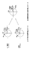
以上の関係を図2に示す。図2(A)において、can-1,cbn-1,can,cbnは、それぞれ周波数a,bのパイロット信号の第(n−1)番目または第n番目のシンボルを位相平面上に示したものであり、θcan-1,θcbn-1,θcan,θcbnはそれぞれの位相量である。ところで、これら第(n−1)番目と第n番目のシンボルに含まれているパイロット信号の周波数は元々等しいはずであるが、前述のような種々の誤差により、図2(A)に示すように位相平面上における位置にずれを生じてくる。そこで、これら第(n−1)番目と第n番目のシンボルの間で差動復調を行うことにより、シンボルによらず一定である誤差(FFT窓位相誤差、再生搬送波位相誤差、および、マルチパス妨害等の伝送路歪みによる位相誤差など)を除去することができる。
【0054】
即ち、図2(B)に示すように、第(n−1)番目と第n番目のシンボルの差動復調を求めると、2つのパイロット信号はI軸の近傍に移動されることになる。なお、この図において、dcan、dcbnは、それぞれ周波数a,bのパイロット信号のシンボル間差動復調後の位相平面上のデータであり、dθcan、dθcbnはそれぞれの位相量であり、クロック周波数誤差およびガウス雑音による位相量に対応している。
【0055】
このようにしてシンボル間で差動復調を行うことにより、クロック周波数誤差およびガウス雑音以外の要素に起因する誤差を除去することができる。次に、ガウス雑音に起因する誤差を除去することを考える。
【0056】
ところで、ガウス雑音による誤差はアトランダムに生じるので、複数のパイロット信号から得られる位相誤差を累積加算することにより、フィルタ(平滑化)効果を用いてこれを除去することができる。その結果、クロック周波数誤差に比例した位相誤差量を得ることが出来るので、これを用いることによりクロック発振回路116を正確に制御してクロック信号を生成することができる。
【0057】
ところで、以上のような制御はディジタル的に行われる(離散的な数値を用いて行われる)ので、隣接する2つのシンボル間の位相変動量が分解能以下になった場合には、それ以上の制御は不可能になる。そこで、本実施の形態においては、位相変動量が隣接する2つのシンボルにより検出される誤差が分解能以下になった場合には、その時点におけるFFT処理後の信号をメモリに記憶させておき、記憶されたデータと新たなデータとの間で差動復調を行うことにより、シンボル間隔以上の時間間隔でクロック位相誤差を検出するようにしている。即ち、このような誤差(量子化誤差)は、時間の経過に応じて累積されるので、比較の対象とする時間を長くすることにより検出可能となる。
【0058】
続いて、図1の実施の形態の動作について説明する。
【0059】
高速フーリエ変換回路112(変換手段)により副搬送波周波数に応じて分解されたIチャンネルデータ501とQチャンネルデータ502は、差動復調回路503に入力される。
【0060】
クロック再生動作の初期においては、差動復調回路503では、IチャンネルデータとQチャンネルデータがその周波数が小さい順にRAM506,507および複素演算回路511にそれぞれ供給される。
【0061】
RAM506,507は制御回路520からの制御信号cにより、各シンボル毎にIチャンネルデータとQチャンネルデータをそれぞれ記憶し、1シンボル時間だけ遅延して出力する。RAM507から出力されたQチャンネルデータは、符号反転回路510により符号が反転されて出力される。Iチャンネルデータ、1シンボル遅延されたIチャンネルデータ、Qチャンネルデータ、および、符号反転されて1シンボル遅延されたQチャンネルデータは、その周波数が小さい順に複素乗算回路511により式(1)に示すような複素乗算が施され、Iチャンネルデータ523およびQチャンネルデータ524として出力される。このような一連の操作がシンボル間の差動復調処理となる。
【0062】
前述のように、以上の操作(差動復調)により、信号に含まれているFFT窓位相誤差、再生搬送波位相誤差等が除去されることになる。
【0063】
差動復調データ523,524はROM512に順次供給され、それらの値に対応するシンボル間位相変動量513が読み出されて、ゲート回路514に供給される。
【0064】
ゲート回路514は、制御回路520の制御に応じて、ROM512から出力されるシンボル間位相変動量513のうち、パイロット信号に対応する成分だけを抽出して出力する。
【0065】
符号反転回路521は、ゲート回路514により抽出されたパイロット信号の符号を反転してセレクタ522に供給する。セレクタ522は、制御回路520によって制御され、入力されたパイロット信号が正の周波数であればゲート回路514から直接入力された位相変動量を選択し、負の周波数であれば符号反転回路521から入力された位相変動量を選択して累積加算回路515に供給する。なお、このような操作によって、図3に示すような、周波数の正負に依存するクロック周波数誤差の位相変動の回転方向を一元化することができる。
【0066】
累積加算回路515は新たなシンボルが入力される直前に制御回路520から供給される制御信号bにより初期化された後、セレクタ522から出力されるパイロット信号の位相誤差量を累積加算する。平均値回路516はシンボル毎に入力される累積された位相誤差量を数シンボルに亘って平均化することにより、前述のように位相誤差量に含まれるガウス雑音成分を除去し、クロック発振回路116を制御する位相誤差量517を生成する。平均値回路516から出力された位相誤差量517は、クロック発振回路116に供給され、その発振周波数を制御する。こような一連の処理により正確なクロック周波数が再生されることになる。
【0067】
ところで、前述のような処理により、クロック周波数の確定処理が完了すると、シンボル間差動復調によって得られる位相誤差量517が分解能以下になり、図4に示す残留クロック周波数誤差領域に入る。即ち、クロック周波数の誤差は、離散的な値として出力されるため、シンボル間差動復調累積位相誤差が0の場合においても、クロック周波数誤差出力は0とはならない場合がある。その場合には、クロック信号をそれ以上精密に制御することはできなくなる。
【0068】
図5は、図4に示す残留クロック周波数誤差領域を位相平面上に表したものである。図の縦軸はQ信号、横軸はI信号をそれぞれ示しており、また、格子は量子化ステップに対応している。いま、図に白丸で示すようなパイロット信号が入力された場合、この信号は、図に示す格子を基準として判定すると、図の黒丸で示す位置のデータと同等に判定される。従って、その場合には、クロック周波数誤差による位相誤差が無視されることになるので、その誤差に対する制御は実行できないことになる。
【0069】
しかしながら、本実施の形態においては、比較回路518が平均値回路516の出力が収束したことを検出した場合は、制御回路520に制御信号を供給することにより、RAM506,507の値を固定化するようになされている。
【0070】
即ち、比較回路518はシンボル間差動復調データが0である場合に対応するデータ519と位相誤差量517とを比較し、これらが等しい場合は制御回路520に制御信号を送る。制御回路520はこの制御信号を受けて、RAM506,507に制御信号cを供給し、その時点において高速フーリエ変換回路112から出力されている復調信号をRAM506,507にそれぞれ記憶させる。以降、差動復調回路503は、RAM506,507に記憶された信号を基準にして差動復調を行うので、位相誤差信号の検出時間がシンボル間時間に比べて長くなり、その結果、シンボル間差動復調で得られる残留クロック周波数誤差以下のクロック周波数誤差を検出して制御することが可能となる。
【0071】
以上の実施の形態によれば、OFDM信号がクロック周波数誤差に伴う位相誤差のみならず、再生搬送波位相誤差、FFT窓位相誤差、ガウス雑音による位相誤差、および、マルチパスによる伝送路ひずみに起因する位相誤差を含む場合においても、クロック信号を正確に再生することが可能となる。
【0072】
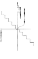
ところで、一般的に、OFDM時間信号の各シンボルは、図6(A)に示すように、有効シンボル期間と有効シンボル期間の一部をコピーしたガード期間とにより構成されている。従って、有効シンボル期間だけ遅延させたOFDM時間信号(図6(B)参照)と元のOFDM時間信号との相関値を、ガード期間幅に亘って算出すると、その値はシンボルの境界で最大値を取る(図6(C)参照)ことになる。
【0073】
なお、受信側のクロック信号が送信側のクロック信号と同期していない場合には、図7に示すように相関値が最大となる位相が時間とともに変化することとなる。即ち、図7(A)に示すように、送信側の送信クロック信号と受信側の再生クロック信号とが正確に同期している場合には、相関値が最大となるタイミングは、常に一定であるが、例えば、送信クロック信号よりも再生クロック信号の周波数の方が高い場合には、相関値が最大となるタイミングは、次第に遅れていくことになる。また、送信クロック信号よりも再生クロック信号の周波数の方が低い場合には、相関値が最大となるタイミングは、次第に進んでいくことになる。従って、このような位相変化量を観測してクロック発振回路116を制御すれば、クロック位相の同期再生を行うことができる。
【0074】
以上のような原理に基づく、本発明の第2の実施の形態を図8に示す。
【0075】
図8にOFDM時間信号の相関値を用いたクロック再生方法の実施の形態の構成例を示すブロック図である。なお、この図においては、説明を簡略化するために、クロック再生部のみに注目し、図10に示す搬送波を再生する部分は省略してある。
【0076】
基底帯域に変換されたOFDM時間信号のIチャンネル成分およびQチャンネル成分は、高速フーリエ変換回路704と相関値演算回路703(遅延手段、演算手段)にそれぞれ入力される。相関値演算回路703はOFDM時間信号の周期性を利用して相関値を算出するようになされている。高速フーリエ変換回路704は、入力されたIチャンネル成分とQチャンネル成分に対してフーリエ変換を施し、Iチャンネルデータ705およびQチャンネルデータ706として出力するとともに、位相誤差検出回路707に供給するようになされている。位相誤差検出回路707は、パイロット信号を用いて位相誤差を検出するようになされており、その詳細については後述する。
【0077】
最大値検出回路708(検知手段)は相関値演算回路703から出力される相関値の最大値をシンボルカウンタ709に同期して検出するようになされている。シンボルカウンタ709はシンボル時間をカウントし、そのカウント値を最大値検出回路708に供給するようになされている。RAM710(保持手段)は、位相誤差検出回路707から制御信号が出力された場合、即ち、位相変動量が分解能以下になった場合に、最大値検出回路708が最大値を検出したシンボルのカウント値を基準位相として記憶するようになされている。
【0078】
位相比較回路711(算定手段)は、RAM710に記憶された基準位相と、シンボル毎にシンボルカウンタ709から供給される最大値が検出された場合のカウント値とを比較し、位相誤差量を検出するようになされている。LPF712は、位相比較回路711から出力される位相誤差量から、雑音成分を取り除いて加算回路713に供給する。加算回路713は、LPF712から出力された位相誤差量と位相誤差検出回路707から出力された位相誤差量とを加算して、D/A変換回路714に出力する。D/A変換回路714は、加算回路713から出力された位相誤差量を、対応するアナログ信号に変換してクロック発振回路116に供給するようになされている。クロック発振回路116は、D/A変換回路714から出力される信号に応じて、所定の周波数のクロック信号を発振するようになされている。
【0079】
次に、図9を参照して、図8に示す位相誤差検出回路707の詳細な構成例について説明する。なお、位相誤差検出回路707は図1の実施の形態で示した構成から、位相記憶部分を除外したものであり、また、図9において、図1と対応する部分には対応する符号を付してあるのでその説明は省略する。
【0080】
この実施の形態では、比較回路518の出力は、RAM710に入力されるようになされている。その他の構成は、図1における場合と同様である。
【0081】
次に、図8および図9を参照して、以上の実施の形態の動作について説明する。
【0082】
クロック再生動作の初期状態においては、第1の実施の形態において説明したように、FFT処理が施された信号に対してシンボル間の差動復調を行うことにより、各副搬送波の位相誤差を求め、更に、この位相誤差信号からパイロット信号を抜き出して累積加算する事により、クロック周波数誤差を検出し、検出された周波数誤差を基準としてクロック信号を再生する。
【0083】
位相誤差検出回路707によるクロック信号の再生が完了すると、誤差値が分解能以下になり、図4に示す残留クロック周波数誤差領域に陥入する。その場合、比較回路518はシンボル間差動復調データが0である場合に対応するデータ519と、位相誤差量517とを比較し、これらが等しい場合はRAM710に制御信号を送る。制御信号を受け取ったRAM710は、その時点で最大値検出回路708が検出した最大値に対応するシンボル位相をシンボルカウンタ709から受け取り、基準位相として記憶する。
【0084】
その後、位相比較回路711はRAM710に記憶された基準位相と、各シンボル毎にシンボルカウンタ709から供給される最大値検出位相とを比較し、位相誤差量を検出する。LPF712は、位相比較回路711から出力された位相誤差量から雑音成分を除去して加算回路713に出力する。加算回路713は、位相誤差検出回路707からの出力と、LPF712の出力を加算してD/A変換回路714に供給する。
【0085】
D/A変換回路714は、加算回路713の出力信号(ディジタル信号)を対応するアナログ信号に変換してクロック発振回路116に出力する。クロック発振回路116は、D/A変換回路714の出力に応じた周波数で発振し、クロック信号を出力する。
【0086】
以上の実施の形態によれば、クロック再生動作の初期においては、位相誤差検出回路707の迅速な制御によりクロック信号の周波数が確定され、クロック信号の周波数誤差が位相誤差検出回路707の検出分解能以下になった場合には、OFDM時間信号の相関値を用いて正確な周波数制御を行うことが可能となる。
【0087】
【発明の効果】
請求項1に記載の受信装置および請求項5に記載の受信方法によれば、OFDM信号を離散的フーリエ変換し、得られた副搬送波の周波数成分を記憶し、記憶されている少なくとも1シンボル前の周波数成分と、新たに得られた周波数成分との間の位相変動量を算出し、算出された位相変動量より、パイロット信号に対応する成分を抽出し、抽出されたパイロット信号に対応する位相変動量を複数のパイロット信号にわたって累積加算し、この累積加算された信号に応じてクロック信号発生手段を制御してクロック信号の周波数を制御するようにしたので、受信したOFDM信号がクロック周波数誤差に伴う位相誤差のみならず、再生搬送波位相誤差、FFT窓位相誤差、ガウス雑音による位相誤差、および、マルチパスによる伝送路ひずみに起因する位相誤差を含む場合においても、正確にクロック信号を生成することが可能となる。
【図面の簡単な説明】
【図1】本発明の実施の形態の構成例を示すブロック図である。
【図2】差動復調前後のパイロット信号を位相平面上に示した図である。
【図3】クロック周波数誤差による位相誤差と副搬送波周波数の関係を示す図である。
【図4】残留クロック周波数誤差領域を示す図である。
【図5】残留クロック周波数誤差領域を位相平面上に示した図である。
【図6】OFDM時間信号と相関値の関係を示す図である。
【図7】相関値の最大値位相とクロック周波数誤差の関係を示す図である。
【図8】本発明の第2の実施の形態の構成例を示すブロック図である。
【図9】図8に示す位相誤差検出回路の構成例を示すブロック図である。
【図10】OFDM受信機の構成例を示すブロック図である。
【図11】従来のコスタス演算を用いたクロック再生装置の構成例を示すブロック図である。
【図12】マルチパス妨害を受けたときのOFDM受信スペクトラムを示す図である。
【符号の説明】
112 高速フーリエ変換回路(変換手段), 506,507 RAM(記憶手段), 511 複素乗算回路(算出手段), 512 ROM(算出手段), 514 ゲート回路(抽出手段), 515 累積加算回路(累積加算手段), 516 制御回路(制御手段), 518 比較回路(検出手段), 520 制御回路(禁止手段), 703 相関値演算回路(遅延回路,演算回路), 708 最大値検出回路(検知手段), 710 RAM(保持手段), 711 位相比較回路(算定手段)[0001]
BACKGROUND OF THE INVENTION
The present invention relates to a receiving apparatus and a receiving method, and more particularly to a receiving apparatus and a receiving method based on the OFDM scheme.
[0002]
[Prior art]
In recent years, a modulation method called orthogonal frequency division multiplexing (OFDM) has been proposed as a method for transmitting digital signals. This OFDM system is a system in which a number of orthogonal subcarriers are provided in a transmission band, data is allocated to the amplitude and phase of each subcarrier, and digital modulation is performed by PSK (Phase Shift Keying) or QAM (Quadrature Amplitude Modulation). . In this method, since the transmission band is divided by a large number of subcarriers, the band per subcarrier is narrowed and the modulation speed is slow. However, since the number of carriers is large, the total transmission speed is the same as the conventional modulation system. And no different.
[0003]
In this OFDM method, since a number of subcarriers are transmitted in parallel, the symbol rate becomes slow. Therefore, in a transmission path in which so-called multipath interference exists, the time length of the multipath relative to the time length of the symbol should be shortened. It can be expected to be a robust system against multipath interference.
[0004]
Due to the above characteristics, the OFDM scheme is particularly attracting attention for the transmission of digital signals by terrestrial waves that are strongly affected by multipath interference. For example, DVB-T (Digital Video Broadcasting-Terrestrial) is well known as such a terrestrial digital signal transmission.
[0005]
Also, with recent advances in semiconductor technology, discrete Fourier transform (hereinafter referred to as FFT (Fast Fourier Transform)) and discrete Fourier transform (hereinafter referred to as IFFT (Invert Fast Fourier Transform)) One of the reasons that the OFDM system has attracted attention is that it can be easily implemented using hardware, and can be easily modulated based on the OFDM system and can be demodulated. is there.
[0006]
FIG. 10 is a block diagram illustrating a configuration example of an OFDM receiver. The
[0007]
The
[0008]
The
[0009]
The correlation
[0010]
The carrier frequency
[0011]
The clock
[0012]
Next, the operation of the above conventional example will be described.
[0013]
The RF signal captured by the
[0014]
The A /
[0015]
The
[0016]
The correlation
[0017]
By the way, in order to correctly demodulate the OFDM signal on the receiving side, various synchronizations are required. For example, first, in order to convert an OFDM signal in the IF band into an OFDM signal in the base band, the frequency oscillated by the numerical
[0018]
Here, as a method for synchronizing the latter clock signal with the transmission side, a conventionally proposed clock recovery method will be described.
[0019]
In the method described below, in addition to the information to be transmitted, a specific signal (hereinafter referred to as a pilot signal) with prescribed amplitude and phase is inserted and transmitted by a predetermined number for each symbol on the transmission side. It is. On the receiving side, a pilot signal interpolated on the transmitting side is extracted from the OFDM signal on which the FFT operation has been performed, and the clock signal is reproduced by performing a Costas operation described below on the pilot signal.
[0020]
FIG. 11 is a configuration example of a conventional clock recovery circuit that recovers a clock signal using Costas arithmetic when the pilot signal is modulated by QPSK (Quadrature Phase Shift Keying). In this figure, gate circuits 208-1 and 208-2 each receive I-channel data and Q-channel data that have been subjected to FFT operation, and extract and output only a pilot signal. The squaring circuits 203-1 and 203-2 square the pilot signals extracted by the gate circuits 208-1 and 208-2 and output them.
[0021]
The
[0022]
Next, the operation of the above conventional example will be described.
[0023]
The I channel data and the Q channel data demodulated by frequency decomposition by the fast
[0024]
[0025]
The
[0026]
A series of operations as described above is a so-called Costas operation, and the phase error of the clock signal can be detected by such a Costas operation. Based on the phase error of the clock signal thus detected, the
[0027]
[Problems to be solved by the invention]
By the way, when the phase error is detected using the above-mentioned Costas calculation and the clock signal is reproduced according to the result, the detected phase error is not only the phase error accompanying the clock frequency error but also reproduced. Carrier phase error, FFT window phase error, phase error due to Gaussian noise, and phase error caused by transmission path distortion due to multipath that cannot be avoided when transmitting terrestrial waves. Therefore, there is a problem that it is difficult to control the clock transmission circuit by extracting only the phase error accompanying only.
[0028]
FIG. 12A shows an example of the spectrum of the OFDM signal, and FIG. 12B shows the spectrum of the OFDM signal when subjected to multipath interference. Here, the thick line represents the pilot signal interpolated on the transmission side. As shown in FIG. 12B, when the transmission signal is subjected to frequency selective interference due to multipath, the signal-to-noise ratio of the pilot signal with respect to other subcarriers is lowered. In such a case, the signal-to-noise ratio of the phase error signal of the clock signal generated from the pilot signal by the method as described above also decreases. As a result, there has been a problem that it is difficult to accurately reproduce the clock signal when the transmission signal is subjected to multipath interference.
[0029]
The present invention has been made in view of the above situation, and the received OFDM signal is not only a phase error due to a clock frequency error, but also a recovered carrier phase error, an FFT window phase error, a phase error due to Gaussian noise, and An object of the present invention is to provide a clock recovery circuit of an OFDM receiver capable of accurately generating a clock signal even when a phase error due to transmission path distortion due to multipath is included.
[0030]
[Means for Solving the Problems]
The receiving apparatus according to
[0031]
Claim 4 The receiving method described in The receiving apparatus is a clock signal generating means for generating a clock signal used in the receiving apparatus, and includes a clock signal generating means capable of controlling the frequency of the clock signal, A transform step for discrete Fourier transform of the OFDM signal, a storage step for storing the frequency component of the subcarrier obtained by the transform step, a frequency component at least one symbol before stored in the storage step, and a new one by the transform step From the calculation step for calculating the amount of phase fluctuation between the frequency components obtained in the above and the amount of phase fluctuation calculated by the calculation step, Pilot signal The extraction step to extract the component corresponding to, and extracted by the extraction step Pilot signal Phase variation corresponding to Is cumulatively added over multiple pilot signals, and this cumulatively added signal In response to the Control the clock signal generation means And a control step for controlling the frequency of the clock signal.
[0034]
In the receiving apparatus according to
[0035]
Claim 4 In the receiving method described in The receiving apparatus is a clock signal generating means for generating a clock signal used in the receiving apparatus, and includes a clock signal generating means capable of controlling the frequency of the clock signal, The transform step performs discrete Fourier transform on the OFDM signal, the storage step stores the frequency component of the subcarrier obtained by the transform step, and the frequency component at least one symbol before stored in the storage step and a new one by the transform step. The calculation step calculates the phase fluctuation amount between the obtained frequency component and the phase fluctuation amount calculated by the calculation step, Pilot signal The extraction step extracts the components corresponding to, and extracted by the extraction step Pilot signal Phase variation corresponding to Is cumulatively added over multiple pilot signals, and this cumulatively added signal In response to the Control the clock signal generation means The control step controls the frequency of the clock signal. For example, the FFT transform circuit, which is the transform step, performs discrete Fourier transform on the OFDM signal, the frequency component of the obtained subcarrier is stored in the memory, which is the memory step, and the frequency component one symbol before stored in the memory The phase fluctuation amount is calculated by differential demodulation of the frequency component newly output from the FFT conversion circuit, and the phase fluctuation amount calculated by the calculation step is calculated. Pilot signal The extraction step extracts the components corresponding to, and extracted by the extraction step Pilot signal Phase variation Is cumulatively added over multiple pilot signals, and this cumulatively added signal In response to the Control the clock signal generation means The control step controls the frequency of the clock signal.
[0038]
FIG. Shows an example of an embodiment of the present invention. In this embodiment, the clock frequency recovery circuit shown in FIG. 115 It is about.
[0039]
In this figure, a differential demodulation circuit 503 includes RAMs (Random Access Memory) 506 and 507. ,
[0040]
The
[0041]
(I + jQ) (I -1 -JQ -1 (1)
[0042]
ROM (Read Only Memory) 512 Is Arc tangent (inverse tangent function) data is stored, and
[0043]
[0044]
The
[0045]
The
[0046]
[0047]
[0048]
Next, the operation of the above embodiment will be described, but before that, the operation principle of this embodiment will be briefly described.
[0049]
For example, when the OFDM signal is regenerated on the receiver side using a clock signal that is not synchronized with the transmission side, the FFT signal phase error and the regenerated carrier phase error that are normally included in the pilot signal demodulated by the FFT process are included. In addition to a phase error due to Gaussian noise and a phase error due to transmission path distortion such as multipath interference, a phase error due to clock signal non-synchronization is included.
[0050]
By the way, except for the phase error due to Gaussian noise and the phase error due to clock signal non-synchronization, the phase error is constant regardless of the symbol. Therefore, if differential demodulation is performed between the signal at a certain reference time and the symbol of the currently observed signal, these phase errors (a constant phase error regardless of the symbol) can be removed. This is expressed as follows.
[0051]
θ nk = Θ k + φ + nkδ + k (1 + δ) τ + Ψ k + ε n ... (2)
θ (n + 1) k = Θ k + φ + (n + 1) kδ + k (1 + δ) τ + Ψ k + ε n + 1 ... (3)
θ (n + 1) k −θ nk = Kδ + ε n + 1 −ε n ... (4)
[0052]
Here, Expression (2) represents the phase data of the kth subcarrier frequency of the nth symbol. And θ k Is the phase specified on the transmitting side, δ is the clock error, φ is the phase error of the recovered carrier, τ is the FFT window phase error, Ψ k Is the phase error due to transmission path distortion such as multipath interference for the kth subcarrier frequency, ε n Indicates the phase error due to the Gaussian noise of the nth symbol. Furthermore, Expression (3) is phase data of the kth subcarrier frequency of the (n + 1) th symbol, Expression (4) is a result of subtracting Expression (2) from Expression (3), This represents the amount of phase fluctuation between the (n + 1) th symbol and the nth symbol of the kth subcarrier frequency after differential demodulation.
[0053]
The above relationship is shown in FIG. In FIG. 2A, ca n-1 , Cb n-1 , Ca n , Cb n Represents the (n−1) th or n th symbol of the pilot signals of frequencies a and b on the phase plane, respectively, and θca n-1 , Θcb n-1 , Θca n , Θcb n Is the amount of each phase. By the way, although the frequencies of the pilot signals included in the (n−1) th and nth symbols should originally be equal, due to various errors as described above, as shown in FIG. The position on the phase plane is shifted. Therefore, by performing differential demodulation between the (n−1) th and nth symbols, errors that are constant regardless of the symbols (FFT window phase error, reconstructed carrier phase error, and multipath) Phase error due to transmission path distortion such as interference) can be removed.
[0054]
That is, as shown in FIG. 2B, when the differential demodulation of the (n−1) th and nth symbols is obtained, the two pilot signals are moved to the vicinity of the I axis. In this figure, dca n , Dcb n Are the data on the phase plane after the inter-symbol differential demodulation of the pilot signals of frequencies a and b, respectively, dθcan and dθcbn are the respective phase amounts, corresponding to the phase amounts due to clock frequency error and Gaussian noise Yes.
[0055]
By performing differential demodulation between symbols in this way, errors due to factors other than clock frequency error and Gaussian noise can be removed. Next, consider removing an error caused by Gaussian noise.
[0056]
By the way, since the error due to Gaussian noise occurs at random, it can be removed using a filter (smoothing) effect by cumulatively adding the phase errors obtained from a plurality of pilot signals. As a result, a phase error amount proportional to the clock frequency error can be obtained. By using this, the
[0057]
By the way, since the control as described above is performed digitally (using discrete numerical values), when the phase fluctuation amount between two adjacent symbols becomes less than the resolution, the control beyond that is performed. Is impossible. Therefore, in the present embodiment, when the error detected by the two adjacent symbols whose phase fluctuation amount is smaller than the resolution, the signal after the FFT processing at that time is stored in the memory and stored. By performing differential demodulation between the generated data and new data, a clock phase error is detected at a time interval equal to or greater than the symbol interval. That is, such an error (quantization error) is accumulated with the passage of time, and can be detected by increasing the time to be compared.
[0058]
Next, the operation of the embodiment of FIG. 1 will be described.
[0059]
The I channel
[0060]
In the initial stage of the clock recovery operation, the differential demodulation circuit 503 supplies the I channel data and the Q channel data to the
[0061]
The
[0062]
As described above, the FFT window phase error, the reproduced carrier phase error, and the like included in the signal are removed by the above operation (differential demodulation).
[0063]
The differential
[0064]
Under the control of the
[0065]
The
[0066]
The
[0067]
By the way, when the determination processing of the clock frequency is completed by the processing as described above, the
[0068]
FIG. 5 shows the residual clock frequency error region shown in FIG. 4 on the phase plane. In the figure, the vertical axis represents the Q signal and the horizontal axis represents the I signal, and the lattice corresponds to the quantization step. Now, when a pilot signal as indicated by a white circle in the figure is input, this signal is determined to be equivalent to the data at the position indicated by the black circle in the figure when determined with reference to the lattice shown in the figure. Therefore, in this case, the phase error due to the clock frequency error is ignored, and control for the error cannot be executed.
[0069]
However, in this embodiment, when the
[0070]
That is, the
[0071]
According to the above embodiments, the OFDM signal is caused not only by the phase error due to the clock frequency error but also by the recovered carrier phase error, the FFT window phase error, the phase error due to Gaussian noise, and the transmission path distortion due to multipath. Even when a phase error is included, the clock signal can be accurately reproduced.
[0072]
By the way, generally, each symbol of the OFDM time signal is composed of an effective symbol period and a guard period obtained by copying a part of the effective symbol period, as shown in FIG. Therefore, when the correlation value between the OFDM time signal delayed by the effective symbol period (see FIG. 6B) and the original OFDM time signal is calculated over the guard period width, the value is the maximum value at the symbol boundary. (See FIG. 6C).
[0073]
When the clock signal on the receiving side is not synchronized with the clock signal on the transmitting side, the phase where the correlation value is maximum changes with time as shown in FIG. That is, as shown in FIG. 7A, when the transmission clock signal on the transmission side and the recovered clock signal on the reception side are accurately synchronized, the timing at which the correlation value is maximized is always constant. However, for example, when the frequency of the recovered clock signal is higher than that of the transmission clock signal, the timing at which the correlation value is maximized is gradually delayed. Further, when the frequency of the recovered clock signal is lower than that of the transmission clock signal, the timing at which the correlation value is maximized gradually proceeds. Therefore, if the
[0074]
FIG. 8 shows a second embodiment of the present invention based on the principle as described above.
[0075]
FIG. 8 is a block diagram illustrating a configuration example of an embodiment of a clock recovery method using a correlation value of an OFDM time signal. In this figure, in order to simplify the explanation, only the clock recovery unit is noted, and the part for recovering the carrier wave shown in FIG. 10 is omitted.
[0076]
The I channel component and the Q channel component of the OFDM time signal converted into the base band are input to the fast
[0077]
The maximum value detection circuit 708 (detection means) detects the maximum correlation value output from the correlation
[0078]
The phase comparison circuit 711 (calculation means) compares the reference phase stored in the
[0079]
Next, a detailed configuration example of the phase
[0080]
In this embodiment, the output of the
[0081]
Next, the operation of the above embodiment will be described with reference to FIGS.
[0082]
In the initial state of the clock recovery operation, as described in the first embodiment, the phase error of each subcarrier is obtained by performing differential demodulation between symbols on the signal subjected to FFT processing. Further, by extracting the pilot signal from the phase error signal and accumulating it, the clock frequency error is detected, and the clock signal is reproduced based on the detected frequency error.
[0083]
When the reproduction of the clock signal by the phase
[0084]
Thereafter, the
[0085]
The D / A conversion circuit 714 converts the output signal (digital signal) of the
[0086]
According to the above embodiment, in the initial stage of the clock recovery operation, the frequency of the clock signal is determined by the rapid control of the phase
[0087]
【The invention's effect】
According to the receiving apparatus according to
[Brief description of the drawings]
FIG. 1 is a block diagram illustrating a configuration example of an embodiment of the present invention.
FIG. 2 is a diagram showing pilot signals before and after differential demodulation on a phase plane.
FIG. 3 is a diagram illustrating a relationship between a phase error due to a clock frequency error and a subcarrier frequency.
FIG. 4 is a diagram illustrating a residual clock frequency error region.
FIG. 5 is a diagram showing a residual clock frequency error region on a phase plane.
FIG. 6 is a diagram illustrating a relationship between an OFDM time signal and a correlation value.
FIG. 7 is a diagram illustrating a relationship between a maximum value phase of a correlation value and a clock frequency error.
FIG. 8 is a block diagram illustrating a configuration example of a second exemplary embodiment of the present invention.
9 is a block diagram showing a configuration example of a phase error detection circuit shown in FIG.
FIG. 10 is a block diagram illustrating a configuration example of an OFDM receiver.
FIG. 11 is a block diagram illustrating a configuration example of a clock recovery device using a conventional Costas operation.
FIG. 12 is a diagram illustrating an OFDM reception spectrum when subjected to multipath interference.
[Explanation of symbols]
112 Fast Fourier transform circuit (transformation means), 506,507 RAM (storage means), 511 complex multiplication circuit (calculation means), 512 ROM (calculation means), 514 gate circuit (extraction means), 515 cumulative addition circuit (cumulative addition) Means), 516 control circuit (control means), 518 comparison circuit (detection means), 520 control circuit (prohibition means), 703 correlation value calculation circuit (delay circuit, calculation circuit), 708 maximum value detection circuit (detection means), 710 RAM (holding means), 711 Phase comparison circuit (calculating means)
Claims (4)
前記OFDM信号を離散的フーリエ変換する変換手段と、
前記変換手段により得られた副搬送波の周波数成分を記憶する記憶手段と、
前記記憶手段に記憶されている少なくとも1シンボル前の前記周波数成分と、前記変換手段により新たに得られた周波数成分との間の位相変動量を算出する算出手段と、
前記算出手段により算出された位相変動量より、前記パイロット信号に対応する成分を抽出する抽出手段と、
前記受信装置において使用されるクロック信号を発生するクロック信号発生手段であって、クロック信号の周波数が制御可能なクロック信号発生手段と、
前記抽出手段により抽出された前記パイロット信号に対応する位相変動量を複数のパイロット信号にわたって累積加算し、この累積加算された信号に応じて前記クロック信号発生手段を制御して前記クロック信号の周波数を制御する制御手段と
を備えることを特徴とする受信装置。 A receiver for pilot signal amplitude and phase are defined to receive the OFDM signal contained in each symbol,
Transform means for discrete Fourier transform of the OFDM signal;
Storage means for storing the frequency component of the subcarrier obtained by the conversion means;
Calculating means for calculating a phase fluctuation amount between the frequency component at least one symbol before stored in the storage means and the frequency component newly obtained by the converting means;
Extraction means for extracting a component corresponding to the pilot signal from the phase fluctuation amount calculated by the calculation means;
Clock signal generating means for generating a clock signal used in the receiving device, the clock signal generating means capable of controlling the frequency of the clock signal;
The phase fluctuation amount corresponding to the pilot signal extracted by the extracting means is cumulatively added over a plurality of pilot signals, and the clock signal generating means is controlled in accordance with the cumulatively added signal to adjust the frequency of the clock signal. And a control means for controlling.
前記検出手段により前記位相変動量が所定の値以下になったことが検出された場合には、前記記憶手段に記憶されている副搬送波の周波数成分の変更を禁止する禁止手段とを更に備える
ことを特徴とする請求項1に記載の受信装置。Detecting means for detecting that the amount of phase fluctuation corresponding to the pilot signal sequence extracted by the extracting means has become a predetermined value or less;
And a prohibiting unit that prohibits a change in the frequency component of the subcarrier stored in the storage unit when the detection unit detects that the phase fluctuation amount is equal to or less than a predetermined value. The receiving apparatus according to claim 1.
前記遅延手段により遅延されたOFDM時間信号と、遅延されていないもとのOFDM時間信号との間の相関値を演算する演算手段と、
前記演算手段の出力の最大値を検知する検知手段と、
前記検知手段により検知されたある時点における最大値の位相を保持する保持手段と、
前記保持手段に保持されている位相と、前記検知手段により新たに検知された最大値の位相のずれを算定する算定手段とを更に備え、
前記制御手段は、前記算定手段により算定された位相のずれと、前記抽出手段により抽出された前記パイロット信号系列に対応する位相変動量とに応じて前記クロック信号の周波数を制御する
ことを特徴とする請求項1に記載の受信装置。Delay means for delaying the OFDM time signal converted to the baseband by an effective symbol period;
Computing means for computing a correlation value between the OFDM time signal delayed by the delay means and the original OFDM time signal not delayed;
Detecting means for detecting the maximum value of the output of the calculating means;
Holding means for holding the phase of the maximum value at a certain point detected by the detecting means;
And further comprising: a phase held in the holding means; and a calculation means for calculating a phase shift of the maximum value newly detected by the detection means,
The control means controls the frequency of the clock signal according to the phase shift calculated by the calculation means and the phase fluctuation amount corresponding to the pilot signal sequence extracted by the extraction means. The receiving device according to claim 1.
前記受信装置は、前記受信装置において使用されるクロック信号を発生するクロック信号発生手段であって、クロック信号の周波数が制御可能なクロック信号発生手段を備えており、
前記OFDM信号を離散的フーリエ変換する変換ステップと、
前記変換ステップにより得られた副搬送波の周波数成分を記憶する記憶ステップと、
前記記憶ステップに記憶されている少なくとも1シンボル前の前記周波数成分と、前記変換ステップにより新たに得られた周波数成分との間の位相変動量を算出する算出ステップと、
前記算出ステップにより算出された位相変動量より、前記パイロット信号に対応する成分を抽出する抽出ステップと、
前記抽出ステップにより抽出された前記パイロット信号に対応する位相変動量を複数のパイロット信号にわたって累積加算し、この累積加算された信号に応じて前記クロック信号発生手段を制御して前記クロック信号の周波数を制御する制御ステップと
を備えることを特徴とする受信方法。 A receiving method in a receiving apparatus for receiving an OFDM signal in which a pilot signal having a prescribed amplitude and phase is included for each symbol ,
The receiver is a clock signal generator for generating a clock signal used in the receiver, and includes a clock signal generator capable of controlling the frequency of the clock signal,
A transforming step for performing a discrete Fourier transform on the OFDM signal;
A storage step of storing the frequency component of the subcarrier obtained by the conversion step;
A calculation step of calculating a phase fluctuation amount between the frequency component at least one symbol before stored in the storage step and the frequency component newly obtained by the conversion step;
An extraction step for extracting a component corresponding to the pilot signal from the phase fluctuation amount calculated in the calculation step;
The phase fluctuation amount corresponding to the pilot signal extracted in the extraction step is cumulatively added over a plurality of pilot signals, and the clock signal generating means is controlled in accordance with the cumulatively added signal to adjust the frequency of the clock signal. And a control step for controlling.
Priority Applications (6)
| Application Number | Priority Date | Filing Date | Title |
|---|---|---|---|
| JP11471097A JP3797397B2 (en) | 1997-05-02 | 1997-05-02 | Receiving apparatus and receiving method |
| US09/069,702 US6215819B1 (en) | 1997-05-02 | 1998-04-29 | Receiving apparatus and receiving method |
| EP98303415A EP0880250B1 (en) | 1997-05-02 | 1998-04-30 | Receiving apparatus and receiving methods |
| ES98303415T ES2264186T3 (en) | 1997-05-02 | 1998-04-30 | APPLIANCE AND RECEPTION METHOD. |
| DE69835254T DE69835254T2 (en) | 1997-05-02 | 1998-04-30 | Receiving devices and receiving methods |
| AU63784/98A AU6378498A (en) | 1997-05-02 | 1998-05-01 | Receiving apparatus and receiving method |
Applications Claiming Priority (1)
| Application Number | Priority Date | Filing Date | Title |
|---|---|---|---|
| JP11471097A JP3797397B2 (en) | 1997-05-02 | 1997-05-02 | Receiving apparatus and receiving method |
Publications (2)
| Publication Number | Publication Date |
|---|---|
| JPH10308715A JPH10308715A (en) | 1998-11-17 |
| JP3797397B2 true JP3797397B2 (en) | 2006-07-19 |
Family
ID=14644693
Family Applications (1)
| Application Number | Title | Priority Date | Filing Date |
|---|---|---|---|
| JP11471097A Expired - Fee Related JP3797397B2 (en) | 1997-05-02 | 1997-05-02 | Receiving apparatus and receiving method |
Country Status (6)
| Country | Link |
|---|---|
| US (1) | US6215819B1 (en) |
| EP (1) | EP0880250B1 (en) |
| JP (1) | JP3797397B2 (en) |
| AU (1) | AU6378498A (en) |
| DE (1) | DE69835254T2 (en) |
| ES (1) | ES2264186T3 (en) |
Families Citing this family (36)
| Publication number | Priority date | Publication date | Assignee | Title |
|---|---|---|---|---|
| EP0903897B1 (en) * | 1997-09-22 | 2001-10-31 | Alcatel | Method and arrangement to determine a clock timing error in a multi-carrier transmission system |
| JP3981898B2 (en) * | 1998-02-20 | 2007-09-26 | ソニー株式会社 | Signal receiving apparatus and method, and recording medium |
| FR2784821B1 (en) * | 1998-10-16 | 2000-12-15 | Cit Alcatel | SPECTRUM SPREAD TRANSMISSION SYSTEM WITH FILTERED MULTI-CARRIER MODULATION |
| JP4272309B2 (en) * | 1998-10-29 | 2009-06-03 | パナソニック株式会社 | OFDM communication device |
| GB9823812D0 (en) * | 1998-10-30 | 1998-12-23 | Mitsubishi Electric Inf Tech | Multicarrier communications systems |
| FR2790344B1 (en) * | 1999-02-26 | 2001-05-18 | St Microelectronics Sa | COFDM DEMODULATOR WITH FFT ANALYSIS WINDOW MOVEMENT COMPENSATION |
| KR100557877B1 (en) * | 1999-04-16 | 2006-03-07 | 전남대학교산학협력단 | Apparatus and method for channel estimating and ofdm system for the same |
| EP1073241A3 (en) | 1999-07-29 | 2006-05-03 | Matsushita Electric Industrial Co., Ltd. | Symbol synchronisation in multicarrier transmission |
| JP3492565B2 (en) * | 1999-09-13 | 2004-02-03 | 松下電器産業株式会社 | OFDM communication device and detection method |
| CN1326087C (en) | 1999-12-28 | 2007-07-11 | 索尼公司 | Signal processing device and method, and recording medium |
| JP3773388B2 (en) * | 2000-03-15 | 2006-05-10 | 三菱電機株式会社 | Clock signal regeneration circuit and clock signal regeneration method |
| GB2361607A (en) * | 2000-04-17 | 2001-10-24 | Mitsubishi Electric Inf Tech | Compensating for local oscillator and sampling frequency offsets in an OFDM receiver |
| JP2002026858A (en) * | 2000-07-03 | 2002-01-25 | Hitachi Kokusai Electric Inc | Transmission device adopting orthogonal frequency division multiplex modulation system |
| JP4003386B2 (en) * | 2000-09-13 | 2007-11-07 | 三菱電機株式会社 | Clock signal reproducing device and receiving device, clock signal reproducing method and receiving method |
| US6754170B1 (en) * | 2000-09-29 | 2004-06-22 | Symbol Technologies, Inc. | Timing synchronization in OFDM communications receivers |
| US6778622B2 (en) * | 2000-12-18 | 2004-08-17 | Schlumberger Technology Corporation | Estimating timing error in samples of a discrete multitone modulated signal |
| US7962162B2 (en) * | 2001-08-07 | 2011-06-14 | At&T Intellectual Property Ii, L.P. | Simulcasting OFDM system having mobile station location identification |
| KR20030047591A (en) * | 2001-12-11 | 2003-06-18 | (주)텔레시스테크놀로지 | Device and method for compensating received signal of orthogonal frequency division multiplexing communication system |
| US7020226B1 (en) | 2002-04-04 | 2006-03-28 | Nortel Networks Limited | I/Q distortion compensation for the reception of OFDM signals |
| JP4043335B2 (en) | 2002-10-08 | 2008-02-06 | 株式会社日立国際電気 | Receiver |
| JP2004214961A (en) * | 2002-12-27 | 2004-07-29 | Sony Corp | Ofdm demodulator |
| US7492841B2 (en) * | 2003-01-30 | 2009-02-17 | Andrew Corporation | Relative phase/amplitude detection system |
| KR100510551B1 (en) * | 2003-10-10 | 2005-08-26 | 삼성전자주식회사 | OFDM demodulator with common phase error(CPE) correction and CPE removing method |
| KR100983272B1 (en) * | 2003-12-22 | 2010-09-24 | 엘지전자 주식회사 | Apparatus for recovering carrier in digital TV receiver |
| US7545870B1 (en) | 2004-04-14 | 2009-06-09 | Panasonic Corporation | Reception device |
| KR100602189B1 (en) * | 2004-07-07 | 2006-07-19 | 삼성전자주식회사 | Method and apparatus for auto-reporting a result of self-test |
| JP4419969B2 (en) | 2006-02-09 | 2010-02-24 | ソニー株式会社 | OFDM demodulator and method |
| JP4645679B2 (en) * | 2008-05-12 | 2011-03-09 | 三菱電機株式会社 | Clock signal reproducing apparatus, receiving apparatus, and clock signal reproducing method |
| JP4766072B2 (en) * | 2008-05-20 | 2011-09-07 | ソニー株式会社 | Communication device |
| US8902831B2 (en) * | 2008-06-17 | 2014-12-02 | Centre Of Excellence In Wireless Technology | Methods and systems for interference mitigation |
| JP2010068194A (en) * | 2008-09-10 | 2010-03-25 | Mitsubishi Electric Corp | Carrier frequency error detection device |
| US8280330B2 (en) * | 2009-12-30 | 2012-10-02 | Quintic Holdings | Crystal-less clock generation for radio frequency receivers |
| US9197400B1 (en) * | 2012-05-21 | 2015-11-24 | Marvell International Ltd. | Method and apparatus for joint estimation of carrier frequency offset and sampling frequency offset |
| US9350587B1 (en) | 2012-11-30 | 2016-05-24 | Marvell International Ltd. | System and method for timing error estimation |
| JP6445286B2 (en) * | 2014-09-08 | 2018-12-26 | 旭化成エレクトロニクス株式会社 | Phase detector, phase adjustment circuit, receiver and transmitter |
| CN109286535B (en) * | 2018-09-06 | 2022-04-01 | 晶晨半导体(上海)股份有限公司 | Method and system for acquiring delay step time in storage module |
Family Cites Families (16)
| Publication number | Priority date | Publication date | Assignee | Title |
|---|---|---|---|---|
| FR2670062B1 (en) | 1990-11-30 | 1993-11-12 | Thomson Csf | METHOD FOR RECALARING THE LOCAL OSCILLATORS OF A RECEIVER AND DEVICE FOR CARRYING OUT THE METHOD. |
| GB2278257B (en) * | 1993-05-05 | 1996-10-02 | British Broadcasting Corp | Receiving equipment for digital transmissions |
| JPH0746217A (en) * | 1993-07-26 | 1995-02-14 | Sony Corp | Digital demodulator |
| JPH0746218A (en) * | 1993-07-28 | 1995-02-14 | Sony Corp | Digital demodulator |
| SE501608C2 (en) | 1994-01-18 | 1995-03-27 | Telia Ab | Procedure and arrangement for synchronization in OFDM modulation |
| WO1995020848A1 (en) | 1994-01-28 | 1995-08-03 | Philips Electronics N.V. | Digital transmission system |
| JP3145003B2 (en) * | 1995-03-23 | 2001-03-12 | 株式会社東芝 | Orthogonal frequency division multiplexing transmission system and transmitter and receiver thereof |
| JP3582139B2 (en) * | 1995-03-31 | 2004-10-27 | ソニー株式会社 | Data demodulator and data transmission method |
| JPH0951321A (en) * | 1995-08-09 | 1997-02-18 | Sony Corp | Radio communication equipment and radio communication method |
| US5825807A (en) * | 1995-11-06 | 1998-10-20 | Kumar; Derek D. | System and method for multiplexing a spread spectrum communication system |
| US5828710A (en) * | 1995-12-11 | 1998-10-27 | Delco Electronics Corporation | AFC frequency synchronization network |
| JPH09307526A (en) * | 1996-05-17 | 1997-11-28 | Mitsubishi Electric Corp | Digital broadcast receiver |
| CA2183140C (en) * | 1996-08-12 | 2001-11-20 | Grant Mcgibney | Ofdm timing and frequency recovery system |
| US5878089A (en) * | 1997-02-21 | 1999-03-02 | Usa Digital Radio Partners, L.P. | Coherent signal detector for AM-compatible digital audio broadcast waveform recovery |
| US5946293A (en) * | 1997-03-24 | 1999-08-31 | Delco Electronics Corporation | Memory efficient channel decoding circuitry |
| JP3726857B2 (en) * | 1997-05-02 | 2005-12-14 | ソニー株式会社 | Receiving apparatus and receiving method |
-
1997
- 1997-05-02 JP JP11471097A patent/JP3797397B2/en not_active Expired - Fee Related
-
1998
- 1998-04-29 US US09/069,702 patent/US6215819B1/en not_active Expired - Lifetime
- 1998-04-30 EP EP98303415A patent/EP0880250B1/en not_active Expired - Lifetime
- 1998-04-30 ES ES98303415T patent/ES2264186T3/en not_active Expired - Lifetime
- 1998-04-30 DE DE69835254T patent/DE69835254T2/en not_active Expired - Lifetime
- 1998-05-01 AU AU63784/98A patent/AU6378498A/en not_active Abandoned
Also Published As
| Publication number | Publication date |
|---|---|
| AU6378498A (en) | 1998-11-05 |
| EP0880250B1 (en) | 2006-07-19 |
| JPH10308715A (en) | 1998-11-17 |
| US6215819B1 (en) | 2001-04-10 |
| ES2264186T3 (en) | 2006-12-16 |
| DE69835254T2 (en) | 2007-06-14 |
| EP0880250A1 (en) | 1998-11-25 |
| DE69835254D1 (en) | 2006-08-31 |
Similar Documents
| Publication | Publication Date | Title |
|---|---|---|
| JP3797397B2 (en) | Receiving apparatus and receiving method | |
| JP3726857B2 (en) | Receiving apparatus and receiving method | |
| JP3041175B2 (en) | OFDM synchronous demodulation circuit | |
| JP3074103B2 (en) | OFDM synchronous demodulation circuit | |
| US6993083B1 (en) | Apparatus and method of OFDM demodulation | |
| EP0896457B1 (en) | Symbol synchronization for MCM signals with guard interval | |
| EP1172982B1 (en) | Carrier recovery in a multicarrier receiver | |
| JP2002511711A (en) | Method and apparatus for fine frequency synchronization in a multi-carrier demodulation system | |
| JPH0746218A (en) | Digital demodulator | |
| JPH09130362A (en) | Receiver and reception method | |
| US4518922A (en) | Decision-directed, automatic frequency control technique for non-coherently demodulated M-ARY frequency shift keying | |
| JP2002511710A (en) | Coarse frequency synchronization in multi-carrier systems | |
| JP3342967B2 (en) | OFDM synchronous demodulation circuit | |
| JPH09219692A (en) | Orthogonal frequency division multiplex transmission system and modulator and demodulator therefor | |
| JP3726856B2 (en) | Receiving apparatus and receiving method | |
| JP3148090B2 (en) | OFDM signal synchronous demodulator | |
| JPH0795175A (en) | Ofdm signal demodulator | |
| JP4003386B2 (en) | Clock signal reproducing device and receiving device, clock signal reproducing method and receiving method | |
| JP2772287B2 (en) | OFDM demodulator | |
| JP2001156742A (en) | Ofdm receiver | |
| JP4108939B2 (en) | Orthogonal frequency division multiplexed signal receiver | |
| JPH09200176A (en) | Ofdm synchronization demodulation circuit | |
| JP2003283458A (en) | Carrier discrimination method, carrier discrimination circuit, and automatic frequency tuning circuit capable of utilizing them | |
| JPH08251136A (en) | Signal transmission device/method and signal reception device/method | |
| JP2009302647A (en) | Carrier frequency reproduction circuit and method of ofdm signal demodulator |
Legal Events
| Date | Code | Title | Description |
|---|---|---|---|
| A977 | Report on retrieval |
Free format text: JAPANESE INTERMEDIATE CODE: A971007 Effective date: 20050627 |
|
| A131 | Notification of reasons for refusal |
Free format text: JAPANESE INTERMEDIATE CODE: A131 Effective date: 20050907 |
|
| A521 | Written amendment |
Free format text: JAPANESE INTERMEDIATE CODE: A523 Effective date: 20051107 |
|
| TRDD | Decision of grant or rejection written | ||
| A01 | Written decision to grant a patent or to grant a registration (utility model) |
Free format text: JAPANESE INTERMEDIATE CODE: A01 Effective date: 20060329 |
|
| A61 | First payment of annual fees (during grant procedure) |
Free format text: JAPANESE INTERMEDIATE CODE: A61 Effective date: 20060411 |
|
| FPAY | Renewal fee payment (event date is renewal date of database) |
Free format text: PAYMENT UNTIL: 20090428 Year of fee payment: 3 |
|
| FPAY | Renewal fee payment (event date is renewal date of database) |
Free format text: PAYMENT UNTIL: 20100428 Year of fee payment: 4 |
|
| FPAY | Renewal fee payment (event date is renewal date of database) |
Free format text: PAYMENT UNTIL: 20100428 Year of fee payment: 4 |
|
| FPAY | Renewal fee payment (event date is renewal date of database) |
Free format text: PAYMENT UNTIL: 20110428 Year of fee payment: 5 |
|
| FPAY | Renewal fee payment (event date is renewal date of database) |
Free format text: PAYMENT UNTIL: 20120428 Year of fee payment: 6 |
|
| FPAY | Renewal fee payment (event date is renewal date of database) |
Free format text: PAYMENT UNTIL: 20130428 Year of fee payment: 7 |
|
| LAPS | Cancellation because of no payment of annual fees |