JP4016652B2 - Recording / playback device, playback device. - Google Patents
Recording / playback device, playback device. Download PDFInfo
- Publication number
- JP4016652B2 JP4016652B2 JP2001387285A JP2001387285A JP4016652B2 JP 4016652 B2 JP4016652 B2 JP 4016652B2 JP 2001387285 A JP2001387285 A JP 2001387285A JP 2001387285 A JP2001387285 A JP 2001387285A JP 4016652 B2 JP4016652 B2 JP 4016652B2
- Authority
- JP
- Japan
- Prior art keywords
- data
- seed
- circuit
- scramble
- bit
- Prior art date
- Legal status (The legal status is an assumption and is not a legal conclusion. Google has not performed a legal analysis and makes no representation as to the accuracy of the status listed.)
- Expired - Fee Related
Links
Images


Landscapes
- Signal Processing For Digital Recording And Reproducing (AREA)
- Optical Recording Or Reproduction (AREA)
Description
【0001】
【発明の属する技術分野】
本発明は、DVDなどの光ディスク装置に関し、特に、光ディスク装置においてデータを媒体に記録する際のデータのスクランブル方法に関するものである。
【0002】
【従来の技術】
一般にDVD−RAMのような書き換え可能な光ディスクでは、ディスクのトラック上に光のパワーにより、記録マークを生成することによって、データが書き込まれる。また、記録マークとそれ以外の箇所における光の反射率の差を利用して、データが読み出される。DVD−RAMでは、グルーブと呼ばれる溝がディスク上に形成されており、溝(ランド)と溝でない部分(グルーブ)の両方にデータを書込むことで高密度化されている。
【0003】
ディスク型の記録媒体を用いた記録再生装置において、トラック上にヘッドを正確に位置づけるための制御をトラッキングという。DVD−RAMでは、ウォブルと呼ばれる微少振動をつけてランドとグルーブが形成されており、これを利用してトラッキングが行われている。しかし、隣接トラックに同じデータが書込まれていると、トラッキング信号が微弱となり、トラッキングが外れやすくなるという問題がある。画像、音声などを扱うDVDでは、無音部分など同じデータを大量に書込むことが良く発生する。この問題を解決するために、同じデータが大量にユーザによって書き込まれても、隣接トラックの書き込みデータが同じにならないように、さまざまな工夫がされていた。
【0004】
たとえば、特開平6−274885号公報に示されるように、セクタの開始をマークから開始するか、マークでないところから開始するかを1トラックごとに変える方法がある。また、STANDARD−ECMA−272に記載されているように、DVD−RAMでは、各フレームのID情報を初期値(シード)としてM系列(ランダム系列)を生成し、それをユーザデータに足し込んでから、ディスクに書き込むなどの方法が取られていた。このようにデータをランダム化することを一般にスクランブルという。
【0005】
他方、光通信の分野では、光通信に適した、周波数特性がフラットなラン長制限符号を作る目的で、ガイデッドスクランブルという方法が用いられていた。これは、ラン長制限符号を作りたいデータの先頭に十分大きな空間を持ったデータを付加して多くの種類のデータを作り、それをそれぞれランダム化して作ったデータの中から、求める特性に近いものを1つ選ぶというものである。このような技術については、例えば、“CODES FOR MASS DATA STORAGE SYSTEMS”K. A. S. IMMINK,SHANNON FOUNDATION PUBLISHER, 1999に詳細に述べられている。また、論文では、“POLYNOMIALS FOR GUIDED SCRAMBLING LINE CODE”, IEEE JOURNAL ON SELECTED AREAS IN COMMUNICATIONS,Vol.13,NO.3,APRIL,1995などに記載がある。
【0006】
また、近年青紫色レーザーを用いた高密度光ディスクが提案されている。このような技術については、例えば、“OPTICAL DISC SYSTEM FOR DIGITAL VIDEO RECORDING”, TATSUYA NARAHARA JPN. J. APPL. PHYS. VOL. 39 (2000) PP. 912-919 PART 1, NO. 2B, FEBRUARY 2000 などに記載されている。
【0007】
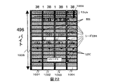
図10に該論文に記載されている光ディスクのフォーマット方法を示す。ユーザデータは64Kbyte単位でエラー訂正符号化され、ディスク媒体上に書き込まれる。光ディスクにおいては、現状のDVD−RAMなどにおいても、2048byte単位で読み書きされ、これを論理セクタと呼ぶ。入力されたユーザデータは、4byteのエラーチェックコードEDCを付加され、2052byteとなる。このEDCを付加した論理セクタを8セクタまとめ、それを216byteずつ76個に分ける。それぞれを[248,216,33]Reed Solomon符号に符号化し、8セクタ分まとめて図10中、網掛けで示す(A)1001の領域(38byte×496byte)に並べる。この38byte×496byteの領域をLDCと呼ぶ。同様に8セクタずつまとめて、(B)1002,(C)1003,(D)1004の領域も埋める。以下、ReedSolomon符号をRS符号と呼ぶ。
【0008】
次に8×4=32セクタ分のアドレス、コピープロテクション情報、代替セクタ情報などを30byteづつに分け、24個の[62,30,33]RS符号に符号化する。これを図10中の3つのBISの領域1005〜1007に8個づつ書き込む。これに同期信号1008を付加したものから、矢印1009に示すように、横方向にデータを取り出し、光ディスク媒体上に書き込む。データ再生時には、光ディスク媒体から読み出されたデータを、矢印1009が示す順番に並べ、図10に示すフォーマットになるように並べた後、エラー訂正処理などを行う。
【0009】
【発明が解決しようとする課題】
ところで、従来技術で紹介した次世代高密度フォーマットを用いた光ディスクでは、光ディスク媒体上の物理的に同じ場所(セクタ)に、同じデータを何度も書くと、媒体が変質し、新しいデータを書いたときに前のデータが残っていてノイズとして見えてくるなどの問題があった。また、光ディスクは可換媒体なので、互換性が重要であり、新しい技術を導入する場合に、従来の新しい技術を導入していない光ディスク媒体を用いる場合でも容易に読み書きできることが必要であった。
【0010】
【課題を解決するための手段】
本発明によるスクランブル方法では、上記問題を解決するために、従来技術で紹介した次世代高密度光ディスクに、任意のシードを用いてデータのスクランブルが行われる。好ましくはディスク上に記録すべき元データに、ランダム化を行うための任意のシードデータが付加される。さらに好ましくは、ディスク上に記録すべき元データにはさらに、セクタナンバー、コピープロテクトなどの付加情報が付加され、アドレスも一緒にスクランブルされる。該ランダム化を行われたデータと付加情報およびシードデータは、エラー訂正符号に符号化される。また、データはLDC領域に、付加情報およびシードはBIS領域に分けて格納するものである。また、本発明のスクランブル方法によれば、1ビットのランダム化データは、1ビットの元データまたはシードデータと複数ビットの過去のランダム化データを用いた演算により決められる。本発明の他の態様によれば、シードデータを必要としないデスクランブル方法が提供される。具体的には、データ再生時、複数ビットのランダム化データを用いた演算により、1ビットのランダム化解除データが決められることを特徴とする。また、本発明の他の態様によれば、1枚のディスクにランダム化が行われている領域とそうでない領域が混在する場合でも、またランダム化に対応しているディスクでも、そうでないディスクでも同じ装置で問題なく読み書きできる。具体的には、読み出しに関してはデータのエラー検出符号や位置情報などを検出しエラーである場合はスクランブルされているものとしてデスクランブルを行うものである。また、書き込みに関しては、
ディスク内に判別情報を格納するエリアを設けるものである。また光ディスク媒体に、スクランブルに対応していない装置でアクセスするための、スクランブルしないで書き込むべき領域と、スクランブルして書き込むべき領域を設けるものである。
【0011】
【発明の実施の形態】
以下、本発明の実施形態について、まず、第1の実施形態を図3〜図9を用いて説明する。図3は本実施形態の光ディスク装置の構成を示す概略ブロック図である。以下に説明する実施形態は、本発明に制限を加えるものではなく、本発明の光ディスク装置は本実施形態のようにコンピュータシステムで用いられる記憶装置の他、テレビと接続される据え置き型画像、音声記録再生装置、携帯ビデオカメラ、携帯音声再生装置などの記録再生装置として用いられる場合もある。
【0012】
図3において、ホストインターフェース(ホストI/F)311は光ディスク装置と図示しないパーソナルコンピュータなどのホストコンピュータとのデータ転送を制御する。スクランブル回路309は、データをランダム化する。エラー訂正符号化回路307は、ランダム化されたデータにエラー訂正符号を付加する。ラン長制限符号化回路305は、エラー訂正符号の付加されたデータを、あらかじめ定められた規則に従って変調し、記録媒体である光ディスク301に記録できるデータに変換する。記録再生アンプ303は、符号化されたデータをラン長制限符号化回路305から受け取り、記録再生ヘッド302に好適な電圧波形に変換する。記録再生ヘッド302は、受け取った電圧波形を光レーザーに変換し、光のパワーにより、光ディスク301上にマークを書込む。データの読み出し時には、記録再生ヘッド302は、レーザ光を光ディスク301に当て、マークと非マークの光の反射強度の差を利用して反射光によりデータを読み出し、読み出した情報を電気信号に変換する。
【0013】
この電気信号は、記録再生アンプ303で適度に増幅された後、データ再生回路304へ出力される。データ再生回路304は読み出されたアナログ信号を0,1のデジタル情報列に変換する。得られたデータ列は、ラン長制限符号復号回路306において、ラン長制限符号化回路305と逆の復調が行われる。エラー訂正回路308では、エラー訂正符号化回路307により付加されたエラー訂正符号をもとに、誤り位置と誤り値を求め、エラーを訂正する。エラーの訂正が行われたデータは、デスクランブル回路310で元のデータに復元される。光ディスク装置では、以上のような手順によってデータの記録再生が行われる。
【0014】
スクランブル回路309について詳細に説明する。図4は、スクランブル回路309の詳細ブロック図である。ホストI/F311から送られたユーザデータは、M系列生成器401にて作られた固定ランダム系列をEOR回路402で足し込まれた後、ランダムシードスクランブル器403に入力される。図5はM系列生成器401の詳細回路図である。502から516はデータを1ビット単位で格納するレジスタであり、入力されるユーザデータに同期してシフト動作を行う。501は排他的論理和回路である。初期状態では、レジスタ516のみが1にセットされ、レジスタ502から514は0にセットされる。本実施形態では、数1に示す15次の多項式によるM系列発生器を仮定している。以下、本実施形態に用いる多項式はすべてガロア体(GF(2))上の多項式であり、“+”は排他的論理和を示す。
【0015】
【数1】

このM系列生成器401によって生成される系列は、2^15−1=32767の周期を持った疑似ランダム系列である。ここで、a^bをaのb乗と定義する。以下、aのb乗をa^bと著す。本実施形態において、M系列生成器401は必ずしも必要ではなく、ランダムシードスクランブル器403だけであってもかまわない。しかし、ランダム性能を良好なものとするために本実施形態では、M系列生成器401も併用する。
【0017】
ランダムシードスクランブル器403では、まず、図9に示すように、データの先頭に8ビットのデータを付加する。これは、任意の8ビットのデータであり、書き込みを行った時間などを基にして作ったデータでも良いし、また8ビットのインクリメントカウンタで書き込みを1回行う毎に1づつインクリメントした値でも良い。この8ビットの付加ビットがランダム化のためのシードとなる。本実施形態では、8ビットのデータを付加するので“00000000”から“11111111”まで2^8=256通りのランダム化ができることになる。すなわち、物理的に同じ場所に同じユーザデータを記録する場合、実際に書込むデータが同じになる確率は1/256になる。隣接トラックに同じユーザデータを書込む場合でも同様である。このようにランダム化を行うことによって、光ディスク301の変質を避けることが可能となり、トラッキングエラーも軽減できる。付加するデータは8ビットである必要はなく、更に多くても、また少なくても良い。また、付加ビット(初期値)はユーザデータの先頭につける必要もなく、ユーザデータのどこに入れても良い。データ(初期値)を付加したところから、後が初期値ごとに異なる系列として生成される。本実施形態では、もっとも効率良くランダム化できる先頭に付加データを置く。
【0018】
図6は2次スクランブル回路405の詳細回路図である。601から604は排他的論理和回路であり、605から612は、データを1ビット単位で格納するレジスタである。レジスタ605から612は、初期状態では0にセットされる。2次スクランブル回路405は、入力データに同期してシフト動作を行う。この回路により、数2に示すスクランブルが行われる。
【0019】
【数2】
ここで、biは2次スクランブル回路に入る前のiビット目のデータ、Ci−jは2次スクランブル回路から出されたiビット目のデータのj ビット前のデータである。この式からわかるように、Ciは1ビットのスクランブル前のデータと複数ビットのスクランブル後の過去のデータから作られる。このようにデータはスクランブルされた後、エラー訂正符号化回路307に送られる。
【0021】
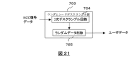
次に、デスクランブル回路310について詳細に説明する。図7はデスクランブル回路310の詳細ブロック図である。図8は図7の2次デスクランブル回路704の詳細回路図である。801から808は1ビット単位でデータを格納するレジスタ。809から812は排他的論理和回路である。2次スクランブル回路704も2次スクランブル回路405と同様入力データに同期してシフト動作を行う。
【0022】
次にデスクランブル回路310の動作について説明する。エラー訂正回路308にてエラーを訂正されたデータは、ランダムシードデスクランブル器703の2次デスクランブル回路704に入力される。2次デスクランブル回路704により、数3に示すデスクランブルが行われる。
【0023】
【数3】
ここで、biはデスクランブルされたiビット目のユーザデータ、ci−jはエラー訂正回路308から入力されたiビット目のjビット前のデータである。この式からわかるように、デスクランブルを行う場合は、スクランブルの初期値が既知でなくてもデスクランブルすることができる。また、エラー訂正回路308にて訂正不可能なエラーが発生した場合、デスクランブルされたユーザデータではエラーが8ビットだけ広がる。しかし、エラー伝播は8ビットだけであり、それ以上広がることはない。
【0025】
次に図9に示すように、ランダムデータ削除回路705にて、ランダムデータ付加回路404にて付加された8ビットの付加ビットを削除する。
【0026】
M系列生成器701は、M系列生成器401と同じであり図5で示される。排他的論理和702で同じ物を加算することにより、ユーザデータは復号される。
【0027】
本実施形態では、ビットシフトするシフトレジスタを用いてスクランブル回路を構成したが、バイト単位で動作する等価な回路でこれを実現しても良い。
また、本実施形態では8ビットの原始多項式
【0028】
【数4】
を用いてランダムシードスクランブルを行ったが、ここで用いる多項式は何を用いても良く、多項式の一般形
【0030】
【数5】
に対してスクランブル回路は図1、デスクランブル回路は図2で実現できる。多項式は、原始多項式を用いると周期が長く取れるので、よりランダムな系列を得ることができる。ここでakは1または0であり、1のとき信号線は接続され、0のとき信号線は接続されない。また、本実施形態は8ビットの原始多項式
【0032】
【数6】
としても表現できる。この場合、多項式の一般形
【0034】
【数7】
に対して、スクランブル回路は図1、デスクランブル回路は図2で実現できる。ここでaiは1または0であり、1のとき信号線は接続され、0のとき信号線は接続されない。数5と数7の関係を一般に相反多項式と呼ぶが、原始多項式の相反多項式は原始多項式であるので、原始多項式を用いるという面では特に問題にならない。数7の定義を用いると、出力データは入力データをスクランブル回路を定義する多項式(ここでは数7)で割った商であるという意味をもつ。しかし、数5、数7のどちらで定義するかはどちらでもよい。
【0036】
また、本実施形態においては、図3におけるスクランブル回路309/デスクランブル回路310はエラー訂正符号化回路307/エラー訂正回路308とホストI/Fの間にいれて説明したが、ラン長制限符号化回路305/復号化回路306とエラー訂正符号化回路307/復号回路308の間に設けられてもよい。さらに、図4及び図7において本実施形態ではM系列生成器401/701をランダムシードスクランブル回路403/デスクランブル回路703よりホストI/F311側に配置しているが、M系列生成器401/701をランダムシードスクランブル403/デスクランブル703より光ディスク301側に配置しても良い。尚、上記したスクランブル回路310またはM系列生成器401/701の配置は1実施例であり、本発明はこれに限定されるものではない。すなわち、スクランブル回路310またはM系列生成器401/701は、本発明の効果を奏することが可能な任意の位置に配置することができる。また、図3においてスクランブル回路309、エラー訂正符号化回路307、ラン長制限符号化回路305、デスクランブル回路310、エラー訂正回路308、ラン長制限符号復号回路306等の全てまたは一部を一チップで構成することも可能である。
【0037】
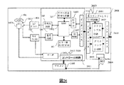
次に第2の実施形態として、第1の実施形態で説明したランダムシードスクランブルを次世代DVDフォーマットに応用した場合について更に詳細に説明する。図14は、本第2の実施形態におけるDVD装置の概略ブロック図である。311は上位装置とのデータの入出力制御を行うインターフェース、1406はシステムを統括するマイコンである。マイコン1406は、システム内のコントロール回路1411に接続され、該コントロール回路1411は図示せざる制御線を介して、シード生成器2603、エラー訂正符号化回路307、スクランブル2601等を制御する。1401はインターフェース311により与えられたユーザデータに、IDなど、記録するのに必要な付加情報を付加するID付加器であり、1402はデータを一時的に貯えておくメモリ(RAM)である。2601はデータをランダム化するスクランブル器である。
【0038】
このスクランブル器は、図20に示すスクランブル器であり、第1の実施形態にて説明したランダムシードスクランブル器403を含む。2603は、スクランブル器2601内のランダムシードスクランブル器に書き込みのたびに異なるシードを与えるシード生成器である。307はスクランブルされたユーザデータに誤り訂正符号を付加するエラー訂正符号化回路、305はエラー訂正符号の付加されたユーザデータを光ディスク301に記録するのに適したラン長制限符号に変換する符号化回路、302は光ディスク301のデータの記録/再生を行うピックアップ、1403はディスクを回転させるスピンドルモータである。また、1404は光ピックアップ302等の制御を行うサーボである。304は、光ディスク301より読み出されたアナログ再生信号の波形等化処理、2値化及び同期クロック生成を行うリードチャネルである。306は、読み出されたラン長制限符号を復号する復号器、308はエラー訂正符号化回路307で付加されたエラー訂正符号をもとにエラーを検出して誤りを訂正するエラー検出訂正回路、2602はスクランブル器2601にて行われたランダム化を解除し、もとのユーザデータに戻す図21に示されるデスクランブル回路であり、第1の実施形態で説明されたランダムシードデスクランブル器703を含む。1407はID付加器1401により付加されたIDなどの記録に必要な付加情報を削除し、ユーザデータのみにするID削除器である。
【0039】
図19は、本第2の実施形態のシード生成器2603を示す図である。1301、1302はともに1ビットシフトレジスタ、1303は排他的論理和回路である。1ビットシフトレジスタ1301には、初期状態において全ゼロ以外の適当な値が入っている。データ書き込み時にシードを要求されると、clock(1305)が入力され、1ビットシフトレジスタ1301、1302の値は左にシフトされる。1ビットシフトレジスタ1302には、排他的論理和回路1303の出力値が入力される。その後、1ビットシフトレジスタ1301、1302に入っているシードの値6ビットとID付加器1401により与えられるセクタID(セクタ番号のb7、b8)(1901)がシード出力線1307を通して、シードとしてスクランブル回路2601に出力される。ここで、セクタIDのb7、b8は、セクタIDの下位から8ビット目と9ビット目に相当し、隣り合ったトラックにおいて絶対に同じ値とならないビットが選択される。
【0040】
以下、図14に示したDVD装置における動作について説明する。まず記録時の動作について、図29に示す光ディスク、図11に示すフォーマットおよび図15に示す記録時の処理手順を参照しながら、説明する。図29に示す光ディスクは、最内周のトラック2901に、本光ディスクがランダムシードスクランブルに対応しているかどうかを示すスクランブルモード情報が書込まれている。スクランブルモード情報は信頼性を持たせるため、2902、2903、2904、2905と同じ情報が4個所に書込まれている。また、本実施形態で示すように最内周に書込むことにより、最内周は傷がつきにくいので、データの信頼性を高く保つことができる。本スクランブルモード情報は光ディスク装置の電源ON時、または光ディスク挿入時に光ディスク装置に読み込まれ、スクランブル回路2601内のモードビット2001に貯えられる。4個所から異なる情報が得られた場合には、多数決により多く読まれた値がモードビット2001に書込まれる。本実施形態においては、スクランブルモード情報の書き込み位置を内周のみに限定したが、内周よりも外周または真ん中あたりのトラックの方が傷がつきにくい場合には、外周または真ん中あたりのトラックに設けてもよい。
【0041】
また、最内周と真ん中あたりの周というように複数のトラックに分けて書いてもよい。この場合、スクランブルモード情報の読み出しに時間はかかるが、よりスクランブルモード情報を高信頼に格納することができる。また本実施形態では、スクランブルモード情報の書き込み位置を4箇所にしたが、さらに多くてもよい。その場合も、よりスクランブルモード情報を高信頼に格納することができる。さらにスクランブルモード情報を高信頼に書き込むために、強力なエラー訂正符号をつけて書き込むこともできる。またスクランブルモード情報の書き込み位置を奇数箇所にした場合は、多数決で必ず決まるため、処理が容易になるというメリットがある。本発明によれば、上記特徴を有するディスクと該ディスクに記録する装置の提供が可能となる。
【0042】
まず、インターフェイス311から2048byte(1論理セクタ分)のユーザデータ1101が入力される(ステップ1501)。ID付加器1401では、インターフェース311から入力されたユーザデータ1101に、4バイトのエラー検出符号(EDC:Error Detection Code)1107を付加し(ステップ1502)、RAM1402領域A1408に書き込む(ステップ1503)。ファイルの終了か確認し(ステップ1504)、終了であれば全部で32セクタになるように、ダミーデータで構成された残りのセクタを追加する(ステップ1517)。ファイルの最後でない場合は、32セクタそろったか確認し(ステップ1505)、32セクタ揃うまでステップ1501〜1505を繰り返す。32セクタ揃ったら、ID付加回路1401ではさらに、図11に示すように、32論理セクタ1101〜1106およびEDC1107〜1112に対して、ID等のデータの識別アドレス情報およびコピープロテクト情報およびリザーブ情報などの付加情報719byte1115を付加する(ステップ1506)。次に、モードビット2001が検査され、今書き込みを行うディスクは、ランダムシードスクランブルに対応しているか判定する(ステップ1507)。
【0043】
対応していない場合には、セレクタ2002は、スクランブルしないユーザデータをエラー訂正検出回路へ転送する。対応している場合には、スクランブル回路2601でスクランブルを行う。スクランブル回路2601では、シード生成器2603により与えられる1byteのシード1114を付加情報719byteの先頭に付加し(ステップ1508)、第1の実施形態で説明したランダムシードスクランブルを行う(ステップ1509)。図11の矢印1116に示すように、左上部から順にシード1114、付加情報1115、ユーザデータ1101の順にスクランブルし、エラー訂正符号化回路307に転送する。
【0044】
次にエラー訂正符号化回路307では、RAM1402内の領域A1408に格納された1byteのランダムシードスクランブル用のシード1114と719byteの付加情報1115をスクランブルしたものを、30byteずつ[62,30,33]RS符号化し、24個に分ける。エラー訂正符号化回路307では、この30byteずつのデータを[62,30,33]RS符号化し、それぞれを図12に示すRAM1402上の領域B(1409)内の3つのBIS領域1005、1006,1007に8符号語ずつ格納する。次に、EDCを付加した論理セクタを8セクタ分ずつまとめ、それを216byteずつ76個に分ける。それぞれを[248,216,33]RS符号に符号化し、8セクタ分まとめて図12中、網掛けで示す(A)のLDC領域1001(38byte×496byte)に並べる。同様に8セクタずつまとめて、(B)1002,(C)1003,(D)1004のLDC領域も埋める(ステップ1510)。さらに、左端に同期信号(SYNC符号)1008を付加する(ステップ1511)。
【0045】
次に符号化回路305は、図12に示される記録再生順を示す矢印1009にしたがってRAM1402上の領域B(1409)からデータを読み出し、31段(1段は縦方向の1バイト分)分を4kbyte分の“物理セクタ”として連続して読み出し(ステップ1512)、ラン長制限符号化する(ステップ1513)。
【0046】
ラン長制限符号されたシーケンスをLDドライバ1405、光ピックアップ302を経て光ディスク301に書き込む(ステップ1514)。その後、光ディスクにデータが正常に書き込まれたか、書き込んだデータを読み出してRAM上のデータと比較する(ステップ1515)。正常に光ディスク301上に1ECCブロック分のデータが記録された場合、処理が終了する。しかし、データを記録する途中で何らかの理由により記録に失敗した場合、同じ場所に同じデータを書込むと媒体の劣化が起こる。したがって、ディスクがランダムシードスクランブルに対応している場合、シードを変えて再スクランブルを行い、データの書き込みをやり直す。すなわち、ステップ1507からやり直す。その場合、RAM1402の領域A1408に格納されたデータが、スクランブル2602でスクランブルされる。スクランブルされたデータはRAM1402に再び格納され、エラー訂正符号化回路307で再びエラー訂正符号が付加される。エラー訂正符号が付加されたデータは、物理セクタに変換され、ラン長制限符号化された後、再度、光ディスク301に書き込まれる。
【0047】
なお、信頼性よりもスピードが重視されるAVシステムのような場合には、ステップ1515および再スクランブルによる再書き込みのステップを省略することも可能である。本実施形態のように書き込み処理を行うことにより、ランダムシードスクランブルのシード1バイトは図12の1201に示すように、BIS領域内に書き込まれることとなる。また、本実施形態のようにランダムシードスクランブルのシードの一部に隣接トラック間で必ず異なるビットを使用することにより、IDなどをシードとしたM系列加算によるスクランブルを行わなくても、隣接トラックと同じデータを書込むことを防ぐことができ、隣接トラックとの相関を少なくすることができるので、サーボなどに対するデータ領域からのノイズを削減することができる。なお、本第2の実施形態ではセクタIDのb7とb8を用いたが、隣接トラック間で異なる値をとることが保証されているものであればなんでも良く、トラック番号などがID中に存在すれば、トラック番号などを用いても良い。現行のDVD−RAMのスクランブルで用いられているM系列のシードのようにIDの一部をトラック情報を与える値としてシードの一部に用いても良い。
【0048】
次に再生時の処理手順について図16を参照して説明する。再生時は、光ピックアップ302によりデータを読み込み、リードチャネル304において2値化及び同期クロック生成を行う(ステップ1601)。復号回路306においてラン長制限符号から復号し(ステップ1602)、図12に示す矢印1009にしたがって、再生データをRAM1402の領域B1409に一時格納する(ステップ1603)。4kbyte相当の物理セクタを16セクタ分まとめて読み出し、RAM1402の領域B1409に一時格納する。エラー検出/訂正回路308において、まず、図12に示すBIS領域に格納されたシード1114およびID等の付加情報719byte1115の誤り訂正処理を行う(ステップ1604)。次に誤り訂正処理を行ったBIS領域に書かれているIDが、再生しようとしているECCブロックのIDであるか確認する(ステップ1605)。ここで、IDが読み出しを希望しているECCブロックまたはセクタのIDであれば、LDC領域の誤り訂正処理を行い(ステップ1614)、ID削除回路1407でID等の付加情報719byte1115を削除して(ステップ1615)、ステップ1611に飛ぶ。誤り訂正処理を行ったBIS領域に書かれているIDが、再生しようとしているECCブロックのIDでない場合には、誤り訂正処理の終了したBIS領域のデータをデスクランブル回路2602に転送し、デスクランブルを行い、RAM1402の領域A1408に一時格納する。(ステップ1606)。
【0049】
本デスクランブル回路2602は、図21に示すように、ランダムシードデスクランブル回路703を含む。BIS領域のデータ入力前には、2次デスクランブル回路704内の1ビットシフトレジスタ801〜808はすべて“0”クリアされている。BIS領域のデスクランブル終了後、LDC領域のデスクランブル開始まで、2次デスクランブル回路704内の1ビットシフトレジスタ801〜808の値は保たれる。次にデスクランブルされたBISデータに含まれているIDが、読み出しを希望しているセクタのIDであるかを確認する(ステップ1607)。読み出したIDが希望しているセクタのIDと異なる場合、再度ステップ1601に戻り、媒体からデータを読み出す。読み出したIDが希望しているセクタのIDである場合、エラー検出/訂正回路308において、LDC領域に格納されたユーザデータの誤り訂正処理を行う(ステップ1608)。誤り訂正処理が終了したら、RAM1402の領域B1409からLDC領域のデータをデスクランブル回路2602に転送し、デスクランブルを行い、RAM1402の領域A1408に一時格納する(ステップ1609)。デスクランブル回路310内の1ビットシフトレジスタ801〜808の値はそのままであるので、続けてデスクランブル処理を行うことができる。デスクランブル終了後、RAM1402の領域A1408に格納されたデータから、ID削除回路1407でスクランブル用シード1114、IDなどの付加情報1115を削除する(ステップ1610)。
【0050】
その後、EDC1107〜1112を用いて、ユーザデータ1101〜1106にエラーのないことを確認し(ステップ1611)、EDC1107〜1112を削除して(ステップ1612)、ユーザデータをインターフェイス311へ出力する(ステップ1613)。このように第2の実施形態の構成とすることにより、エラー訂正処理終了後にスクランブルを解除しているので、ランダムシードスクランブルのエラー伝播によるエラー訂正能力の劣化は発生しない。また、第2の実施形態では、1ECCブロック64Kbyteに1byteのシードを付加させたが、論理セクタ2Kbyte毎にシードを付加させ、論理セクタ毎にランダムシードスクランブルを行うこともできる。また論理セクタ毎にスクランブルする場合でも、1ECCブロックでは各論理セクタが同じシードを用いてランダムシードスクランブル処理する方法が考えられる。
【0051】
また、ランダムシードスクランブルはエラー伝播が発生するので、エラー訂正不能な場合に少しでもデータを救済することを考えると、エラー訂正符号化よりユーザ側でスクランブル処理を行うことが望ましい。また本実施形態にて示したように、ユーザデータに対応するIDなどの付加情報がユーザデータよりも先にデスクランブル処理されることが望ましい。このようにすることにより、IDを早く確認することができるので、IDが誤っている場合の再読み込みを早く行うことができる。また、本実施形態で示したようにデータスクランブル前にIDを確認し、そこで所望のIDが得られた場合にはデータをデスクランブルせずに再生し、所望のIDが得られなかった場合はデスクランブルを行ってからIDを確認し、所望のIDが得られたら、データもデスクランブルして再生することにより、ランダムシードスクランブルを用いて記録されているディスクも、用いないで記録されているディスクも気にすることなく再生できる。また本方式を用いれば、ディスク単位ではなく、スクランブルされているECCブロックとスクランブルされていないECCブロックとが1枚のディスクの中に混在している場合でも、気にすることなく再生できる。本発明によれば、該ディスク、該ディスクを再生する装置の提供が可能となる。
【0052】
また、本実施形態においては、1論理セクタのEDCチェック結果のみで判定を行ったが、複数論理セクタまたは1ECCブロック分のEDCチェック結果がすべてOKの場合には、データにスクランブルがかかっていないと判定しても良い。この場合、EDCの誤検出による判定ミスの確率を減らすことができる。
【0053】
次にECCブロック64KByteの中の一部のセクタのみを書き換える場合の処理手順について図31を参照して説明する。まず、インターフェイス311から書き換えを行うべき2048byte(1論理セクタ分)のユーザデータ1101が入力される(ステップ3101)。ID付加回路1401では、インターフェース311から入力されたユーザデータ1101に、4バイトのエラー検出符号(EDC:Error Detection Code)1107を付加し(ステップ3102)RAM1402の領域A1408に書き込む(ステップ3103)。ファイルの終了か確認し(ステップ3104)、終了でなければステップ3101に戻り、ファイルの最後までデータを読み込む。ファイルの終了の場合、光ディスク301から書き込みを行うECCブロックのデータを読み出す(ステップ3105)。復号回路306においてラン長制限符号から復号し(ステップ3106)、図12に示す矢印1009にしたがって、再生データをRAM1402の領域B1409に一時格納する(ステップ3107)。4kbyte相当の物理セクタを16セクタ分まとめて読み出し、RAM1402の領域B1409に一時格納する。エラー検出/訂正回路308において、まず、図12に示すBIS領域に格納されたシード1114およびID等の付加情報719byte1115の誤り訂正処理を行う(ステップ3108)。誤り訂正処理の終了したIDが書き込みを行いたいECCブロックのIDかを確認し(ステップ3109)、IDが一致した場合は、LDC領域のエラー訂正処理を行い(ステップ3123)、ステップ3114に進む。IDが一致しない場合は、誤り訂正処理の終了したBIS領域のデータをデスクランブル回路2602に転送し、デスクランブルを行い、RAM1402の領域A1408に一時格納する。(ステップ3110)。BIS領域のデータ入力前には、2次デスクランブル回路704内の1ビットシフトレジスタ801〜808はすべて“0”クリアされている。
【0054】
BIS領域のデスクランブル終了後、LDC領域のデスクランブル開始まで、2次デスクランブル回路704内の1ビットシフトレジスタ801〜808の値は保たれる。次にデスクランブルされたBISデータに含まれているIDが、書き込みを希望しているセクタのIDであるかを確認する(ステップ3111)。読み出したIDが希望しているセクタのIDと異なる場合、再度ステップ3105に戻り、媒体からデータを読み出す。読み出したIDが希望しているセクタのIDである場合、エラー検出/訂正回路308において、LDC領域に格納されたユーザデータの誤り訂正処理を行う(ステップ3112)。誤り訂正処理が終了したら、RAM1402の領域B1409からLDC領域のデータをデスクランブル回路310に転送し、デスクランブルを行い(ステップ3113)、ステップ3103にて書き込みが行われていないセクタのみ、RAM1402の領域A1408に一時格納する(ステップ3114)。
【0055】
これで、書き込みを行う1ECCブロック分のデータが揃うことになる。次にスクランブル回路2601では、まず挿入されているディスクがスクランブル対応ディスクかをチェックし(ステップ3115)、スクランブル対応ディスクでなければステップ3118に進む。スクランブル対応ディスクであれば、ランダムシードスクランブルを行う。シード生成器2603により与えられる1byteのランダムシードスクランブル用のシード1114を付加し(ステップ3116)、スクランブルする(ステップ3117)。図11の矢印1116に示すように、左上部から順にシード1114、付加情報1115、ユーザデータ1101の順にスクランブルし、エラー訂正符号化回路307に転送する。
【0056】
次にエラー訂正符号化回路307では、RAM1402内の領域A1408に格納された1byteのランダムシードスクランブル用のシード1114と719byteの付加情報1115をスクランブルしたものを、30byteずつ[62,30,33]RS符号化し、24個に分ける。エラー訂正符号化回路307では、この30byteずつのデータを[62,30,33]RS符号化し、それぞれを図12に示すRAM1402上の領域B1409内の3つのBIS領域1005、1006,1007に8符号語ずつ格納する。次に、EDCを付加した論理セクタを8セクタ分ずつまとめ、それを216byteずつ76個に分ける。それぞれを[248,216,33]RS符号に符号化し、8セクタ分まとめて図12中、網掛けで示す(A)のLDC領域1001(38byte×496byte)に並べる。同様に8セクタずつまとめて、(B)1002,(C)1003,(D)1004のLDC領域も埋める(ステップ3118)。
【0057】
次に符号化回路305は、図12に示される記録再生順を示す矢印1009にしたがってRAM1402上の領域Bからデータを読み出し、31段(1段は縦方向の1バイト分)分を4kbyte分の“物理セクタ”として連続して読み出し(ステップ3119)、ラン長制限符号化する(ステップ3120)。ラン長制限符号化された4kbyte分のデータは、LDドライバ1405、光ピックアップ302を経て光ディスク301に書き込まれる(ステップ3121)。残りのエラー訂正符号化されたデータに関しても同様に、4kbyte単位の“物理セクタ”毎に処理され光ディスク上に書き込まれる。その後、光ディスクにデータが正常に書き込まれたか、書き込んだデータを読み出してRAM上のデータと比較する(ステップ3122)。正常に光ディスク301上に1ECCブロック分のデータが記録された場合、処理が終了する。しかし、データを記録する途中で何らかの理由により記録に失敗した場合、同じ場所に同じデータを書込むと媒体の劣化が起こる。したがって、ディスクがランダムシードスクランブルに対応している場合、シードを変えて再スクランブルを行い、データの書き込みをやり直す。
【0058】
すなわち、ステップ3115からやり直す。その場合、RAM1402の領域Aに格納されたデータが、スクランブル2602でスクランブルされる。スクランブルされたデータはエラー訂正符号化回路307で再びエラー訂正符号が付加される。エラー訂正符号が付加されたデータは、物理セクタに変換され、ラン長制限符号化された後、再度、光ディスク301に書き込まれる。なお、信頼性よりもスピードが重視されるAVシステムのような場合には、ステップ3122および再スクランブルによる再書き込みのステップを省略することも可能である。
【0059】
次に第3の実施形態について図28、図30を参照して説明する。図30は、本第3の実施形態に用いられる光ディスク媒体301である。3001は、光ディスク301の最内周のトラックであり、3001〜3002には、各ECCブロックの書き換え回数が記録されるようになっている。本第3の実施形態の光ディスク301は、図22に示すフォーマットにしたがって書かれており、最内周トラック3001〜トラック3002もまた、図22に示すフォーマットにしたがって書かれている。本実施形態においても、最内周に書き換え回数記録エリアを設けることにより、書き換え回数記録エリアの信頼性を高めている。図22に示すフォーマットでは、図11に示すように32論理セクタ(32*2048byte)分のデータを格納できる。この32*2048byteを17ビットずつの大きさに分け、書き換え回数記録エリアとする。この17ビットの書き換え回数記録エリアは、ディスク全体のデータ記録用ECCブロックに1つずつ対応づけられて、好ましくは約13万回の書き換えまでカウントできるようになっている。光ディスクの工場出荷時には1が書き換え回数として書込まれている。1つのECCブロックで30840個のECCブロックのデータを管理できる。22.5Gbyteの光ディスクを管理するためには、12ECCブロック分の書き換え回数記録エリアが必要になる。最内周トラック3001から12ECCブロック分のトラック(トラック3002まで)が書き換え回数記録エリアとして用意される。
【0060】
図28は、本第3の実施形態におけるDVD装置の概略ブロック図である。311は上位装置とのデータの入出力制御を行うインターフェース、1406はシステムを統括するマイコンである。マイコン1406は、システム内のコントロール回路1411に接続され、該コントロール回路1411は図示せざる制御線を介して、エラー訂正符号化回路307、スクランブル2601等を制御する。マイコン1406内には、現在挿入されている光ディスクが書き換え回数をシードの一部としたランダムシードスクランブルに対応しているかどうかを示す情報ビット2805がある。1401はインターフェース311により与えられたユーザデータに、IDなど、記録するのに必要な付加情報を付加するID付加器であり、1402はデータを一時的に貯えておくメモリ(RAM)である。2601はデータをランダム化するスクランブル器であり、このスクランブル器は、第1の実施形態で説明したものであり、固定シードのM系列生成器およびランダムシードスクランブル器を含む。307はスクランブルされたユーザデータに誤り訂正符号を付加するエラー訂正符号化回路、305はエラー訂正符号の付加されたユーザデータを光ディスク301に記録するのに適したラン長制限符号に変換する符号化回路、302は光ディスク301のデータの記録/再生を行うピックアップ、1403はディスクを回転させるスピンドルモータである。また、1404は光ピックアップ302等の制御を行うサーボである。304は、光ディスク301より読み出されたアナログ再生信号の波形等化処理、2値化及び同期クロック生成を行うリードチャネルである。306は、読み出されたラン長制限符号を復号する復号器、308はエラー訂正符号化回路307で付加されたエラー訂正符号をもとにエラーを検出して誤りを訂正するエラー検出訂正回路、310はスクランブル器309にて行われたランダム化を解除し、もとのユーザデータに戻す第1の実施形態でも示されたデスクランブル回路であり、固定シードのM系列生成器およびランダムシードデスクランブル器を含む。1407はID付加器1401により付加されたIDなどの記録に必要な付加情報を削除し、ユーザデータのみにするID削除器である。
【0061】
メモリ2604は、図23に示すように、光ディスク301のトラック3001〜3002から読み出した書き換え回数を記録するメモリ2301と、1ビットレジスタ2302、インバータ2303により構成されている。データの書き込み時にランダムシードスクランブル用のシードが要求されると、CLOCK2304が入力され、1ビットレジスタ2302の値が反転する。書き換え回数記録メモリ2301に記録されている、書き込みを行うECCブロックの書き換え回数の下位7ビットと1ビットレジスタ2302の値をあわせた8ビットがランダムシードスクランブルのシードとしてスクランブル回路2601に出力される。
【0062】
次に本第3の実施形態では、好ましいラン長制限符号の系列を得るために第2のシードを用いて再スクランブルを行う。再スクランブル用のシードが要求されると、再度CLOCK2304が入力され、1ビットレジスタ2302の値が反転する。書き換え回数記録メモリ2301に記録されている、書き込みを行うECCブロックの書き換え回数の下位7ビットと1ビットレジスタ2302の値をあわせた8ビットがランダムシードスクランブルのシードとしてスクランブル回路2601に出力される。最初に与えられる第1のシードと第2のシードは下位1ビットのみが反転している。なお本シード生成器は1例であり、シフトレジスタ2302を2ビット以上にして、1回の書き込みにつき4通り以上のシードの選択ができるようにしても良い。
【0063】
以下、図28に示した光ディスク装置における動作について説明する。まず電源ON時、または光ディスクの挿入時の動作について、図32をもとに説明する。まず、光ディスク装置に電源が入れられると(ステップ3201)、光ディスク装置2801は光ディスク301が装置内に入っているかを確認する(ステップ3202)。入っていなければ、ステップ3202を繰り返し、光ディスク301が挿入されるのを待つ。光ディスクが挿入されると(ステップ3203)、書き換え回数記録エリア(トラック3001〜トラック3002)に書かれているディスク全体のECCブロックの書き換え回数情報を読み出す(ステップ3204)。まずラン長制限符号復号し(ステップ3205)、RAM1402に格納する(ステップ3206)。BIS領域のエラー訂正を行い(ステップ3207)、BIS領域に書かれているIDを確認する(ステップ3208)。本第3の実施形態においては、BIS領域はスクランブルされていないので、デスクランブル処理は行われない。
【0064】
IDが書き換え回数記録エリアのものであれば、LDC領域のエラー訂正を行い(ステップ3209)、EDCによるエラー検出を行う(ステップ3210)。EDCによりエラーが検出されない場合には、挿入されている光ディスクが書き換え回数をシードの一部とするランダムシードスクランブルに対応していない場合なので、情報ビット2805をリセットして(ステップ3217)終了する。EDCによりエラーが検出された場合には、データをデスクランブルして(ステップ3211)、再度EDCによるエラー検出を行う(ステップ3212)。EDCによりエラーが検出されたら、ステップ3204からやり直す。EDCによりエラーが検出されない場合には、付加されていたシード、ID情報などを削除して(ステップ3213)、EDCを削除して(ステップ3214)、情報ビット2805をセットして(ステップ3215)、メモリ2604に書き換え回数のデータを格納する(ステップ3216)。電源ON時またはディスク挿入時の動作を終了し、ホストインターフェイスからコマンドが与えられるのを待つ。
【0065】
次に記録時の動作について、図22に示すフォーマットおよび図33、図34、図24に示す記録時の処理手順を参照しながら、説明する。
【0066】
まず、図33に示すようにインターフェイス311から、書き込みを行うセクタについての情報を与えられると、ID付加回路1401では、ID等のデータの識別アドレス情報およびコピープロテクト情報およびリザーブ情報などの付加情報を生成して、エラー訂正符号化回路307に入力するとともに、RAM1402上の領域A2802および領域B2803のBIS領域の中の格納場所に格納する(ステップ3301)。領域A2802および領域B2803は、それぞれ図22に示すようにデータを格納するように分けられており、付加情報は、1005、1006、1007で示されるBIS領域に格納される。BIS領域には、ランダムシードスクランブルのシードを格納するシード格納領域2201が設けられており、2物理ブロックに1バイトのシードが格納できるように作られている。次に情報ビット2805を参照し(ステップ3302)、現在書き込みを行おうとしている光ディスクがランダムシードスクランブルに対応していなければ、図24のステップ2401に進み、インターフェイス311から32セクタ分のユーザデータを読み込んだ後、固定シードによる第1次スクランブルを行い(ステップ2402)、エラー訂正符号化した後(ステップ2403)、RAM1402に書き込み(ステップ2404)、同期信号を付加した後(ステップ2405)、ラン長制限符号化して(ステップ2406)、LDドライバ1405、光ピックアップ302を経て光ディスク301に書き込まれる(ステップ2407)。
【0067】
その後、光ディスクにデータが正常に書き込まれたか、書き込んだデータを読み出してRAM上のデータと比較する(ステップ2408)。正常に光ディスク301上に1ECCブロック分のデータが記録された場合、処理が終了する。しかし、データを記録する途中で何らかの理由により記録に失敗した場合、ステップ2406からやり直す。すなわち、RAM1402上のデータをラン長制限符号に変換するところからやり直す。
【0068】
情報ビット2805がセットされていて、現在書き込みを行っている光ディスク301がランダムシードスクランブルに対応しているときは、まずメモリ2604から書き込みを行うECCブロックに対応する書き換え回数を読み出し(ステップ3303)、書き換え回数に“1”を加えメモリ2604に格納する(ステップ3304)。この時、書き換え回数が一定の値、たとえば8万回を超える場合には、媒体劣化により信頼性が低くなることを予想して異なる物理的なセクタへの置き換え処理を行う。そのため代替セクタ処理(ステップ3308)を行い、再度ステップ3301に戻り、IDなどを付け直して記録処理をやり直す。書き換え回数が一定の値以下の場合、インターフェイス311から32論理セクタ分のユーザデータを読み込み(ステップ3306)、まずスクランブル回路2601に送られ、IDの一部などを使った固定シードによるM系列の加算による第1次スクランブルを行う(ステップ3307)。ステップ3309以降の処理は、2物理ブロックずつ処理を行う。1物理ブロックは、図22上で31段(1段は縦方向の1バイト分)分を示す。
【0069】
まず最初の2物理ブロックを処理する場合について説明する。“1”だけ加算された書き換え回数の下位7ビットと1ビットレジスタ2302の出力からなる第1のシードを、RAM1402上の領域A2802内の図22に示すシード2201のひとつ、今処理を行っている物理ブロック内のシード(一番上のシード)に格納する(ステップ3309)。次に現在処理している最初の2物理ブロック内のBIS領域のデータをエラー訂正符号化回路307で、[62,30,33]RS符号化する(ステップ3310)。次にランダムシードスクランブル回路のシフトレジスタを第1のシードでセットする(ステップ3311)。最初の2物理ブロック分のユーザデータをランダムシードスクランブルする。このとき、図22に示す、記録再生順の矢印1009の順番でランダムシードスクランブルする(ステップ3312)。処理を行っている物理ブロックが、7,8セクタ目または15,16セクタ目の場合(ステップ3313)、ユーザデータが途中までしかないので[248,216,33]RS符号に符号化し(ステップ3314)、RAM1402上の領域A2802に書き込む(ステップ3315)。同期信号を付加し(ステップ3316)、ラン長制限符号化する(ステップ3317)。
【0070】
次に第1のシードに対し下位1ビットのみが反転している第2のシードをRAM1402上の領域B2803内の図22に示すシード2201のひとつ、今処理を行っている物理ブロック内のシード(一番上のシード)に格納する(ステップ3318)。次に現在処理している最初の2物理ブロック内のBIS領域のデータをエラー訂正符号化回路307で、[62,30,33]RS符号化する(ステップ3319)。次にランダムシードスクランブル回路のシフトレジスタを第2のシードでセットする(ステップ3320)。最初の2物理ブロック分のユーザデータをランダムシードスクランブルする。このとき、図22に示す、記録再生順の矢印1009の順番でランダムシードスクランブルする(ステップ3321)。処理を行っている物理ブロックが、7,8セクタ目または15,16セクタ目の場合(ステップ3322)、ユーザデータが途中までしかないので[248,216,33]RS符号に符号化し(ステップ3323)、RAM1402上の領域B2803に書き込む(ステップ3324)。同期信号を付加し(ステップ3325)、ラン長制限符号化する(ステップ3326)。ステップ3317とステップ3326で作られた2つのラン長制限符号上のシーケンスのうち、性質のよいものを選び(ステップ3327)、LDドライバ1405、光ピックアップ302を経て光ディスク301に書き込む(ステップ3328)。
【0071】
ここで、性質の良いシーケンスの選び方としては、(1)最大マーク、最大スペースの大きさが小さいものを選ぶ。(2)符号の低域周波数成分の低いものを選ぶ。(3)最小マーク、最小スペースの発生頻度の少ないものを選ぶなどいろいろな方法が考えられる。
【0072】
次に、選ばれたシーケンスが第2のシードから生成されたものである場合は、シード、およびランダムシードスクランブルされたシーケンスをRAM1402上の領域B2803から領域A2802に移す。また、選ばれたシーケンスが第1のシードから生成されたものである場合は、シード、およびランダムシードスクランブルされたシーケンスをRAM1402上の領域A2802から領域B2803に移す。(ステップ3329)。1ECCブロック分終了するまで、繰り返す(ステップ3330)。1ECCブロック分終了したら、光ディスクにデータが正常に書き込まれたか、書き込んだデータを読み出してRAM上のデータと比較する(ステップ3331)。正常に光ディスク301上に1ECCブロック分のデータが記録された場合、処理が終了する。
【0073】
しかし、データを記録する途中で何らかの理由により記録に失敗した場合、同じ場所に同じデータを書込むと媒体の劣化が起こる。したがって、この場合シードを変えて再スクランブルを行い、データの書き込みをやり直す。すなわち、図34に示す処理を行う。まず、メモリ2604に格納された対応するECCブロックの書き換え回数を読み出し(ステップ3401)、書き換え回数に“1”を加えメモリ2604に格納する(ステップ3402)。書き換え回数の下位7ビットと1ビットレジスタ2302の出力からなる第1のシードを、RAM1402上の領域A2802内の図22に示すシード2201のひとつ、今処理を行っている物理ブロック内のシード(一番上のシード)に格納する(ステップ3403)。このとき、書き換え回数は1だけ加算されているのでシードは1回目のときとは必ず異なるシードとなる。次に現在処理している最初の2物理ブロック内のBIS領域のデータをエラー訂正符号化回路307で、[62,30,33]RS符号化する(ステップ3404)。次にRAM1402上の領域A2802内に格納されている最初の2物理ブロック分のランダムシードスクランブルされたデータをデスクランブルする(ステップ3405)。
【0074】
次にランダムシードスクランブル回路のシフトレジスタを第1のシードでセットする(ステップ3406)。次にデスクランブルされたユーザデータをランダムシードスクランブルする。このとき、図22に示す、記録再生順の矢印1009の順番でランダムシードスクランブルされる(ステップ3407)。処理を行っている物理ブロックが、7,8セクタ目または15,16セクタ目の場合(ステップ3408)、ユーザデータが途中までしかないので[248,216,33]RS符号に符号化し(ステップ3409)、RAM1402上の領域A2802に書き込む(ステップ3410)。同期信号を付加し(ステップ3411)、ラン長制限符号化する(ステップ3412)。次に第1のシードに対し下位1ビットのみが反転している第2のシードをRAM1402上の領域B2803内の図22に示すシード2201のひとつ、今処理を行っている物理ブロック内のシード(一番上のシード)に格納する(ステップ3413)。
【0075】
次に現在処理している最初の2物理ブロック内のBIS領域のデータをエラー訂正符号化回路307で、[62,30,33]RS符号化する(ステップ3414)。次にランダムシードスクランブル回路のシフトレジスタを第2のシードでセットする(ステップ3415)。ステップ3405で得られたユーザデータをランダムシードスクランブルする。このとき、図22に示す、記録再生順の矢印の順番でランダムシードスクランブルされる(ステップ3416)。処理を行っている物理ブロックが、7,8セクタ目または15,16セクタ目の場合(ステップ3417)、ユーザデータが途中までしかないので[248,216,33]RS符号に符号化し(ステップ3418)、RAM1402上の領域B2803に書き込む(ステップ3419)。同期信号を付加し(ステップ3420)、ラン長制限符号化する(ステップ3421)。ステップ3412とステップ3421で作られた2つのラン長制限符号上のシーケンスのうち、性質のよいものを選び(ステップ3422)、LDドライバ1405、光ピックアップ302を経て光ディスク301に書き込む(ステップ3423)。
【0076】
次に、選ばれたシーケンスが第2のシードから生成されたものである場合は、シード、およびランダムシードスクランブルされたシーケンスをRAM1402上の領域B2803から領域A2802に移す。また、選ばれたシーケンスが第1のシードから生成されたものである場合は、シード、およびランダムシードスクランブルされたシーケンスをRAM1402上の領域A2802から領域B2803に移す(ステップ3424)。1ECCブロック分終了するまで、繰り返す(ステップ3425)。1ECCブロック分終了したら、光ディスクにデータが正常に書き込まれたか、書き込んだデータを読み出してRAM上のデータと比較する(ステップ3426)。正常に光ディスク301上に1ECCブロック分のデータが記録された場合、処理が終了する。
【0077】
次に再生時の動作について、図25の処理手順を参照しながら説明する。まず光ディスク装置2801は光ディスクからデータを読み出す(ステップ2501)。まずラン長制限符号復号し(ステップ2502)、RAM1402に格納する(ステップ2503)。BIS領域のエラー訂正を行い(ステップ2504)、BIS領域に書かれているIDを確認する(ステップ2505)。本第3の実施形態においては、BIS領域はスクランブルされていないので、デスクランブル処理は行われない。IDが読み出し要求にあったECCブロックのものであれば、LDC領域のエラー訂正を行い(ステップ2506)、EDCによるエラー検出を行う(ステップ2507)。EDCによりエラーが検出されない場合には、ステップ2510に進む。EDCによりエラーが検出された場合には、データをデスクランブルして(ステップ2508)、再度EDCによるエラー検出を行う(ステップ2509)。EDCによりエラーが検出されたら、ステップ2501からやり直す。EDCによりエラーが検出されない場合には、付加されていたシード、ID情報などを削除して(ステップ2510)、EDCを削除して(ステップ2511)、インターフェイス311から復号したユーザデータを出力する(ステップ2512)。このように制御することにより、1枚のディスクにランダムシードスクランブルされている領域とそうでない領域が混在する場合でも、特にそれを示すフォーマット上の特別なビットなどを設けることなく、簡単に読み出しを行うことができる。
【0078】
次に電源OFF時および光ディスク取り出し時の動作について、図36に示す処理手順を参照しながら、説明する。電源OFF命令または光ディスク取り出し命令発生時、光ディスク装置2801は、まず情報ビット2805を参照し(ステップ3603)、情報ビット2805がクリアされている場合にはステップ3606に進む。情報ビット2805がセットされている場合には、メモリ2604のデータを読み出し(ステップ3604)、書き換え回数記録エリアに対応する書き換え回数カウントをすべて1だけカウントアップする(ステップ3605)。その後、図33の書き込みシーケンスのステップ3307以降の書き込みシーケンスに従いメモリ2604に格納されていた書き換え回数をディスク301のトラック3001から3002に書き込み(ステップ3606)、その後、光ディスクの取り出し、電源OFFを行う(ステップ3606)。
【0079】
本第3の実施形態にて示したように複数のRLLシーケンスを生成した後で、シーケンスの特性の良いものを1つ選ぶことにより、性質の良いシーケンスからなるディスクを作る技術は、特にROMディスク作成装置において有効である。ROMディスク作成装置においても、本第3の実施形態と同様に構成できる。
【0080】
また第3の実施形態によれば、複数のシーケンスから選ぶことにより、より性質の良いラン長符号シーケンスを得ることができる。
【0081】
次に第4の実施形態について図18および図13を参照して説明する。図18は、本第4の実施形態に示される光ディスク装置2801の概略ブロック図である。311は上位装置とのデータの入出力制御を行うインターフェース、1406はシステムを統括するマイコンである。マイコン1406は、システム内のコントロール回路1411に接続され、該コントロール回路1411は図示せざる制御線を介して、シード生成器2603、エラー訂正符号化回路307、スクランブル2601等を制御する。1401はインターフェース311により与えられたユーザデータに、IDなど、記録するのに必要な付加情報を付加するID付加器であり、307はユーザデータに誤り訂正符号を付加するエラー訂正符号化回路、1402はデータを一時的に貯えておくメモリ(RAM)である。2601はデータをランダム化するスクランブル器であり、このスクランブル器は、第1の実施形態で説明したものであり、固定シードのM系列生成器およびランダムシードスクランブル器を含む。305はスクランブル処理されたユーザデータを光ディスク301に記録するのに適したラン長制限符号に変換する符号化回路、302は光ディスク301のデータの記録/再生を行うピックアップ、1403はディスクを回転させるスピンドルモータである。
【0082】
また、1404は光ピックアップ302等の制御を行うサーボである。304は、光ディスク301より読み出されたアナログ再生信号の波形等化処理、2値化及び同期クロック生成を行うリードチャネルである。306は、読み出されたラン長制限符号を復号する復号器、310はスクランブル器309にて行われたランダム化を解除し、もとのユーザデータに戻す第1の実施形態でも示されたデスクランブル回路であり、固定シードのM系列生成器およびランダムシードデスクランブル器を含む。308はエラー訂正符号化回路307で付加されたエラー訂正符号をもとにエラーを検出して誤りを訂正するエラー検出訂正回路、1407はID付加器1401により付加されたIDなどの記録に必要な付加情報を削除し、ユーザデータのみにするID削除器である。2603は、スクランブル器309に書き込み処理のたびに、新たなシードを生成して与えるシード生成器である。
【0083】
以下、図18に示した光ディスク装置における動作について図17を参照して説明する。まず記録時、ホストインターフェイス311から入力されたユーザデータにID付加器1401にてIDなどの記録するのに必要な付加情報を付加する。その後、エラー訂正符号化回路307にてエラー訂正符号化し、RAM1402に図12に示すフォーマットにしたがって格納した後、物理セクタ単位で読み出し、固定シードによるスクランブルを行った後、シード生成器2603から与えられたシードをRAMから読み出すデータの先頭に付加してランダムシードスクランブルを行い、ラン長制限符号化回路305にてラン長制限符号化して、光ディスク301に書込む。その後、光ディスクに正常に書込めたか、読み出して確認する。正常に書込めていなかった場合には、RAM1402に格納されているデータにたいし、再度固定シードを用いたスクランブルを行い、シードを変えてランダムシードスクランブルを行い、ラン長制限符号化回路305にてラン長制限符号化して、光ディスク301に書込む。光ディスクに書込む際には、図13に示すフォーマットにしたがって書込む。すなわち、セクタ生成のために、光ディスク上に形成されているHeader3702、Mirror3703に続いて書込み開始タイミングのずれを吸収するGap3704、Guard3705、再生クロックを生成するためのVFO領域3706、バイト同期を取るためのPS3707に続いて、スクランブル後のシード1バイト3708が書き込まれる。
【0084】
その後、ユーザデータが図12のフォーマットにしたがって、書込まれる。またシードの格納場所としては、図12に示すBIS領域1005、1006、1007のうち、使われていない領域に埋め込んでも良い。次に、再生時の動作について説明する。再生時は、まず光ディスクから読み出したデータをラン長制限符号復号回路に306で復号し、シードをデータの先頭位置3708、またはBIS領域1005、1006、1007から取り出し、デスクランブル回路310にてランダムシードデスクランブル、固定シードスクランブルのデスクランブルを行い、RAM1402に格納する(ステップ3206)。エラー訂正回路308にてエラー訂正処理を行い、付加されていたID情報などを削除して、ホストインターフェイスに出力する。
【0085】
本実施形態に示すようにランダムシードスクランブルをエラー訂正回路より媒体側に置くことにより、書き直し処理においてエラー訂正符号化処理を省くことができるので、高速に書き直し処理を実行できる。
【0086】
次に第5の実施形態について、図26を参照して説明する。第5、第6、第7の実施形態はエラー訂正符号化回路などを内蔵する既存の光ディスク制御LSIにより制御される光ディスク装置に、ランダムシードスクランブルを適用する方法について述べる。まず、第5の実施形態においては、ランダムシードスクランブル処理を行うスクランブルLSI2605は、光ディスク制御LSI2611よりもホストインターフェイス側に置かれる。スクランブルLSI2605にはホストコンピュータとのデータ入出力制御を行う2610と、スクランブル回路2607、デスクランブル回路2609、ホストコンピュータのインターフェイス回路と同様の信号を出力し、光ディスク制御LSI2611上のインターフェイス回路311とのデータ入出力制御を行うインターフェイス回路2608を含む。シード生成器2613、スクランブル回路2607、デスクランブル回路2609は、第2の実施形態にて説明したものと同じである。また、マイコン1406は、スクランブルLSI2605内のコントロール回路2614に接続され、該コントロール回路2614は図示せざる制御線を介して、シード生成器2613、スクランブル2607等を制御する。
【0087】
次に記録時の動作について、説明する。まずインターフェイス311から、書き込みを行うセクタについてのデータの大きさ、記録場所のIDなどの情報を与えられると、インターフェイス2608を通して、光ディスク制御LSI2611に与えられた情報をそのまま伝える。次にインターフェイス2610から、第1の1論理セクタ分(2048byte)のユーザデータを受け取ると、シード生成器2613は新しいシードを生成し、スクランブル回路2607に渡す。スクランブル回路2607では、1論理セクタ分のユーザデータの先頭にシードを付加し、スクランブルを行う。スクランブル後のシーケンスの最初の1バイトは、マイコン1406によって読み出され、続く2048byteのスクランブル後のシーケンスはインターフェイス2608を通して光ディスク制御LSI2611に転送される。次に第2の1論理セクタ分(2048byte)のユーザデータを受け取ると、その論理セクタが前期第1の論理セクタと同じECCブロックに書かれるべきデータの場合、シード生成器2613は新しいシードを生成しない。
【0088】
その論理セクタが前期第1の論理セクタと異なるECCブロックに書かれるべきデータの場合、シード生成器2613は新しいシードを生成する。このようにして1ECCブロック分のユーザデータを読み込む。光ディスク制御LSI2611では、ID付加回路1401で前期セクタ情報から、ID等のデータの識別アドレス情報およびコピープロテクト情報およびリザーブ情報などの付加情報720byteを生成し、RAM1402に図12に示すフォーマットで書き込む。図12に示す3つのBIS領域1005、1006,1007に書き込む。マイコン1406は、RAM1402上のBIS領域1005、1006,1007の中の前記付加情報720byte中の固定値で書かれるリザーブ領域に、さきほど読み出したスクランブルされたシーケンスの最初の1byteを書き込む。マイコン1406によって書き込まれた1byteを含む付加情報720byteを30byteずつ24個に分ける。エラー訂正符号化回路307では、この30byteずつのデータを[62,30,33]RS符号化し、それぞれを図12に示すRAM1402上の3つのBIS領域1005、1006,1007に8符号語ずつ格納する。
【0089】
次にインターフェイス311から、2048byte(1論理セクタ分)のユーザデータ1101を読み込む。ID付加器1401では、インターフェース311から入力されたユーザデータに、4バイトのエラー検出符号(EDC:Error Detection Code)を付加し、RAM1402に格納する。次にエラー訂正符号化回路307に転送し、それを216byteずつ[248,216,33]RS(Reed Solomon)符号に符号化し、図12に示すRAM1402上の4つのLDC領域1001、1002、1003、1004に格納する。1ECCブロック分のユーザデータを読み込んでエラー訂正符号化したら、さらに左端に同期信号(SYNC符号)1008を付加する。次に符号化回路305は、図12に示される記録再生順を示す矢印1009にしたがってRAM1402からデータを読み出し、31段(1段は縦方向の1バイト分)分を4kbyte分の“物理セクタ”として連続して読み出し、ラン長制限符号化する。ラン長制限符号化された4kbyte分のデータは、LDドライバ1405、光ピックアップ302を経て光ディスク301に書き込まれる。
【0090】
次に再生時の処理手順について説明する。再生時は、光ピックアップ302によりデータを読み込み、リードチャネル304において2値化及び同期クロック生成を行う。復号回路306においてラン長制限符号から復号し、図12に示す矢印1009にしたがって、再生データをRAM1402に一時格納する。エラー検出/訂正回路308において、まず、図12に示すBIS領域に格納されたスクランブルされたシーケンスの最初の1byteを含むID等の付加情報720byteの誤り訂正処理を行う。次に誤り訂正処理を行ったBIS領域に書かれているIDが、再生しようとしているECCブロックのIDであるか確認する。ここで、IDが読み出しを希望しているECCブロックまたはセクタのIDであれば、まずマイコン1406がBIS領域に格納されたスクランブルされたシーケンスの最初の1byteを読み出し、該1byteが格納されていたRAM上のデータをリザーブ領域の固定値に戻す。それからLDC領域の誤り訂正処理を行い、ID削除回路1407でID等の付加情報720byteを削除して、EDCを用いてエラーチェックを行った後、ユーザデータ2048byteをインターフェイス311、2608を経て、デスクランブル回路2609に転送する。マイコン1406は、BIS領域から読み出したスクランブルされたシーケンスの最初の1byteをユーザデータ2048byteの先頭に付加し、デスクランブルを行う。デスクランブルされたシーケンスは、インターフェイス2610からホストコンピュータに転送される。
【0091】
このように第5の実施形態の構成とすることにより、エラー訂正処理終了後にスクランブルを解除しているので、ランダムシードスクランブルのエラー伝播によるエラー訂正能力の劣化は発生しない。また、第5の実施形態では、1ECCブロックでは各論理セクタが同じシードを用いてランダムシードスクランブル処理したが、1ECCブロック64Kbyteを連続してスクランブルする方法も考えられる。また論理セクタ毎に異なるシードを用いてランダムシードスクランブル処理する方法が考えられる。この場合はBIS領域にスクランブル後の先頭バイトの格納を行う領域として、32byteの領域を確保する必要がある。
【0092】
また、ランダムシードスクランブルはエラー伝播が発生するので、エラー訂正不能な場合に少しでもデータを救済することを考えると、エラー訂正符号化よりユーザ側でスクランブル処理を行うことが望ましい。
【0093】
次に第6の実施形態について、図27を参照して説明する。第6の実施形態においては、ランダムシードスクランブル処理を行うスクランブルLSI2701は、光ディスク制御LSI2611よりも光ディスク媒体側に置かれる。スクランブルLSI2701にはラン長制限符号の復号回路2704、2706と、符号化回路2702、2705、スクランブル回路2703、デスクランブル回路2707、シード生成器2708を含む。スクランブル回路2703、デスクランブル回路2707は、第3の実施形態にて説明したものと同じである。シード生成器は第2の実施形態で説明したものと同じである。
【0094】
次に記録時の動作について、説明する。まずインターフェイス311から、書き込みを行うセクタについての情報を与えられると、光ディスク制御LSI2611では、ID付加回路1401で前期セクタについての情報から、ID等のデータの識別アドレス情報およびコピープロテクト情報およびリザーブ情報などの付加情報720byteを生成し、RAM1402に図12に示すフォーマットで書き込む。図12に示す3つのBIS領域1005、1006,1007に書き込む。ID付加回路1401で生成した付加情報720byteを30byteずつ[62,30,33]RS符号化し、24個に分ける。エラー訂正符号化回路307では、この30byteずつのデータを[62,30,33]RS符号化し、それぞれを図12に示すRAM1402上の3つのBIS領域1005、1006,1007に8符号語ずつ格納する。
【0095】
次にインターフェイス311から、2048byte(1論理セクタ分)のユーザデータ1101を読み込む。ID付加器1401では、インターフェース311から入力されたユーザデータに、4バイトのエラー検出符号(EDC:Error Detection Code)を付加し、RAM1402に格納する。次にエラー訂正符号化回路307に転送し、それを216byteずつ[248,216,33]RS符号に符号化し、図12に示すRAM1402上の4つのLDC領域1001、1002、1003、1004に格納する。1ECCブロック分のユーザデータを読み込んでエラー訂正符号化したら、さらに左端に同期信号(SYNC符号)1008を付加する。
【0096】
次に符号化回路305は、図12に示される記録再生順を示す矢印1009にしたがってRAM1402からデータを読み出し、31段(1段は縦方向の1バイト分)分を4kbyte分の“物理セクタ”として連続して読み出し、ラン長制限符号化する。ラン長制限符号化された4kbyte分のデータは、スクランブルLSI2701に転送される。スクランブルLSI2701では、ラン長制限符号化された4kbyte分のデータを復号回路2704でユーザデータに戻す。シード生成器2708で生成した1byteのシードは、BIS領域のリザーブ領域に埋め込まれ、ランダムシードスクランブル器のプリセット値として用いられる。復号されたユーザデータは、スクランブル器2703でスクランブル処理した後、再度符号化回路2702でラン長制限符号化される。LDドライバ1405、光ピックアップ302を経て光ディスク301に書き込まれる。
【0097】
次に再生時の処理手順について説明する。再生時は、光ピックアップ302によりデータを読み込み、リードチャネル304において2値化及び同期クロック生成を行う。復号回路2706においてラン長制限符号から復号し、BIS領域に埋め込まれたシードが取り出される。取り出されたシードはデスクランブル回路2707内のランダムシードデスクランブル器のプリセット値として用いられる。デスクランブルされたシーケンスは再び符号化回路2705でラン長制限符号化され、光ディスク制御LSI2611に送られる。光ディスク制御LSI2611では、再度ラン長制限符号を復号し、図12に示す矢印1009にしたがって、再生データをRAM1402に一時格納する。エラー検出/訂正回路308において、まず、図12に示すBIS領域に格納されたID等の付加情報720byteの誤り訂正処理を行う。次に誤り訂正処理を行ったBIS領域に書かれているIDが、再生しようとしているECCブロックのIDであるか確認する。
【0098】
ここで、IDが読み出しを希望しているECCブロックまたはセクタのIDであれば、LDC領域の誤り訂正処理を行い、ID削除回路1407でID等の付加情報719byteを削除して、EDCを用いてユーザデータ2048byteのエラーチェックを行う。その後、ユーザデータ2048byteは、インターフェイス311を経て、ホストコンピュータに転送される。このように第6の実施形態の構成とすることにより、既存の光ディスク制御LSI2611にスクランブルLSI2701を付加することにより、ランダムシードスクランブルを適用することができる。
【0099】
次に第7の実施形態について図35を参照して説明する。第7の実施形態においては、ランダムシードスクランブル処理は、マイコン1406でソフト的に処理される。
【0100】
次に記録時の動作について、説明する。まずインターフェイス311から、書き込みを行うセクタについての情報を与えられると、光ディスク制御LSI2611では、ID付加回路1401で前期セクタについての情報から、ID等のデータの識別アドレス情報およびコピープロテクト情報およびリザーブ情報などの付加情報720byteを生成する。マイコン1406は数8で示される演算を行うことにより、シードを決定する。
【0101】
【数8】
ここで、kはk回目のシード生成であることを示す。nは適当な256と互いに疎である数である。マイコン1406により生成された1byteのシードは、制御線3801を通してID付加回路1401で生成された720byteの中のリザーブ領域に書込まれる。720byteは、30byteずつ24個に分けられる。エラー訂正符号化回路307では、この30byteずつのデータを[62,30,33]RS符号化し、それぞれを図12に示すRAM1402上の3つのBIS領域1005、1006,1007に8符号語ずつ格納する。
【0103】
次にインターフェイス311から、2048byte(1論理セクタ分)のユーザデータ1101を読み込む。ID付加器1401では、インターフェース311から入力されたユーザデータに、4バイトのエラー検出符号(EDC:Error Detection Code)を付加し、RAM1402に格納する。次にマイコン1406は制御線3802を通して数2で表される演算をRAMに格納されたデータに対して行うことによりスクランブルを行う。
【0104】
【数2】
この演算において、biは読み込まれるi番目のユーザデータである。RAM1402上のユーザデータの先頭から1bitずつ、データを読み込み、biに代入することによって演算を行う。ciはi番目の演算結果であり、スクランブル後の値である。マイコン1406は、ciの値をRAMに書込む。マイコンによって生成された1byteのシードは数2を演算する上でのc−7からc0の初期値として用いられる。
【0106】
マイコン1406によるスクランブルが終了したら、エラー訂正符号化回路307に転送し、それを216byteずつ[248,216,33]RS(Reed Solomon)符号に符号化し、図12に示すRAM1402上の4つのLDC領域1001、1002、1003、1004に格納する。1ECCブロック分のユーザデータを読み込んでエラー訂正符号化したら、さらに左端に同期信号(SYNC符号)1008を付加する。次に符号化回路305は、図12に示される記録再生順を示す矢印1009にしたがってRAM1402上の領域B1409からデータを読み出し、31段(1段は縦方向の1バイト分)分を4kbyte分の“物理セクタ”として連続して読み出し、ラン長制限符号化する。ラン長制限符号化された4kbyte分のデータは、LDドライバ1405、光ピックアップ302を経て光ディスク301に書き込まれる。
【0107】
次に再生時の処理手順について説明する。再生時は、光ピックアップ302によりデータを読み込み、リードチャネル304において2値化及び同期クロック生成を行う。復号回路306においてラン長制限符号から復号する。図12に示す矢印1009にしたがって、再生データはRAM1402に一時格納される。エラー検出/訂正回路308において、図12に示すBIS領域に格納されたID等の付加情報720byteの誤り訂正処理を行う。次に誤り訂正処理を行ったBIS領域に書かれているIDが、再生しようとしているECCブロックのIDであるか確認する。
【0108】
ここで、IDが読み出しを希望しているECCブロックまたはセクタのIDであれば、LDC領域の誤り訂正処理を行う。次にマイコン1406は、BIS領域に書かれているシードを読み出し、数3の演算をRAM上に格納されたユーザデータに対して行う。
【0109】
【数3】
1byteのシードは数3を演算する上でのc−7からc0の初期値として用いられる。biはスクランブル後のiビット目の値、ciは読み出されたシーケンスの先頭からiビット目の値である。
【0111】
スクランブル終了後、ID削除回路1407でID等の付加情報720byteを削除する。その後、EDCを用いてユーザデータ2048byteのエラーチェックを行う。その後、ユーザデータ2048byteは、インターフェイス311を経て、ホストコンピュータに転送される。このように第7の実施形態の構成とすることにより、既存の光ディスク制御LSI2611を変更することなくソフトウエアのみの処理にてランダムシードスクランブルを適用することができる。そのため、既存の光ディスク制御LSIが搭載されているシステムにおいても、少ない変更を行うことにより、ランダムシードスクランブルを適用できる。
【0112】
次に第8の実施形態について説明する。一般に、コンピュータ用記録媒体として光ディスクを用いる場合には、オーディオ用として光ディスクを用いる場合よりも多くの書き換え回数に耐えられることが必要であるといわれている。それは、コンピュータがディスク内に書き込まれているFAT(File Allocation Table)を頻繁に書き換えながらディスク管理を行うためであり、FATが書き込まれている領域には、一般のデータが書きこまれる領域よりも10倍以上の書き換えが発生するといわれている。ところで本実施形態における光ディスクドライブ3904は、ファイル管理を光ディスクドライブ3904内で行うオブジェクトコマンド対応インターフェイスを持った光ディスクドライブであるとし、ホストコンピュータ3905からは、具体的な物理アドレスではなく、ファイル名で書き込み、読み出しを行うものとする。図37は、本実施形態に用いられる光ディスク媒体301である。本光ディスク媒体301は、ランダムシードスクランブルを行って書き込まれる領域3702、ランダムシードスクランブルを行わずに書き込まれる領域3701および3703に分けられている。3702と3703にはそれぞれ、FATがスクランブルされた形と、スクランブルされない形で、それぞれ書き込まれる。
【0113】
図39は、本第8の実施形態におけるDVD装置の概略ブロック図である。311は上位装置とのデータの入出力制御を行い、ファイル名と物理アドレスの変換を行う。1406はシステムを統括するマイコンである。マイコン1406は、インターフェイス311に接続され、インターフェイス311を制御する。またマイコン1406は、システム内のコントロール回路1411に接続され、該コントロール回路1411は図示せざる制御線を介して、シード生成器2603、エラー訂正符号化回路307、スクランブル2601等を制御する。1401はインターフェース311により与えられたユーザデータに、IDなど、記録するのに必要な付加情報を付加するID付加器であり、1402はデータを一時的に貯えておくメモリ(RAM)である。3902はデータをランダム化するスクランブル器である。このスクランブル器は、図45に示すスクランブル器であり、固定シードのM系列生成器およびランダムシードスクランブル器を含む。これは第1の実施形態で説明したものとほとんど同じであるが、ランダムシードスクランブルをするかしないかを選択できるスイッチ4506がついている点が第1の実施形態と異なる。スイッチ4506は、マイコンによって制御されるランダムシードスクランブルON/OFFを示す信号線4507によって制御される。3901は、スクランブル器3902内のランダムシードスクランブル器に書き込みのたびに異なるシードを与えるシード生成器である。307はスクランブルされたユーザデータに誤り訂正符号を付加するエラー訂正符号化回路、305はエラー訂正符号の付加されたユーザデータを光ディスク301に記録するのに適したラン長制限符号に変換する符号化回路、302は光ディスク301のデータの記録/再生を行うピックアップ、1403はディスクを回転させるスピンドルモータである。また、1404は光ピックアップ302等の制御を行うサーボである。
【0114】
304は、光ディスク301より読み出されたアナログ再生信号の波形等化処理、2値化及び同期クロック生成を行うリードチャネルである。306は、読み出されたラン長制限符号を復号する復号器、308はエラー訂正符号化回路307で付加されたエラー訂正符号をもとにエラーを検出して誤りを訂正するエラー検出訂正回路、3903はスクランブル器3902にて行われたランダム化を解除し、もとのユーザデータに戻すデスクランブル回路であり、このデスクランブル器は、図46に示すデスクランブル器であり、固定シードのM系列生成器4601およびランダムシードデスクランブル器4603を含む。これは第1の実施形態で説明したものとほとんど同じであるが、ランダムシードデスクランブルをするかしないかを選択できるスイッチ4606がついている点が第1の実施形態と異なる。スイッチ4606は、マイコンによって制御されるランダムシードスクランブルON/OFFを示す信号線4607によって制御される。1407はID付加器1401により付加されたIDなどの記録に必要な付加情報を削除し、ユーザデータのみにするID削除器である。
【0115】
図40は、本第8の実施形態のシード生成器3901を示す図である。1301、1302はともに1ビットシフトレジスタ、1303は排他的論理和回路である。1ビットシフトレジスタ1301には、初期状態において全ゼロ以外の適当な値が入っている。データ書き込み時にシードを要求されると、clock(1305)が入力され、1ビットシフトレジスタ1301、1302の値は左にシフトされる。1ビットシフトレジスタ1302には、排他的論理和回路1303の出力値が入力される。その後、1ビットシフトレジスタ1301、1302に入っているシードの値8ビットシード出力線1307を通して、シードとしてスクランブル回路3902に出力される。
【0116】
以下、図39に示したDVD装置における動作について説明する。まず記録時の動作について、図37に示す光ディスクおよび図41に示す記録時の処理手順を参照しながら、説明する。
【0117】
まず、インターフェイス311から書き込みを行うファイル名およびファイルの大きさが入力されると(ステップ4101)、マイコン1406は、領域3703に格納されているFATを読み出し(ステップ4102)、書き込みを行うファイルの大きさから書き込みを行う物理アドレスを算出する(ステップ4103)。次にインターフェイス311から書き込みを行うデータを取り込み(ステップ4104)、ステップ4103で算出した物理アドレスにより示される領域3701内の場所にランダムシードスクランブルなしで書き込みを行う(ステップ4105)。
【0118】
次にFATを更新し、ランダムシードスクランブルなしでFATを領域3703に書き込む(ステップ4106)。次に同じFATをランダムシードスクランブルして領域3702に書き込む(ステップ4107)。次に領域3703に書き込んだFATを読み出し、エラーなく書き込めているかをチェックする(ステップ4107)。領域3703はスクランブルすることなく書き込んでいるので、領域3702よりも媒体劣化が早く、早くエラーが発生するようになる。ステップ4107でエラーがエラー訂正可能範囲内でおさまっている場合には、書き込み処理を終了する。ステップ4107でエラーがエラー訂正可能範囲より多くなっている場合には、領域3702に格納されているFATを読み出しデスクランブルして領域3704に格納する。以後FAT領域として領域3704を使用する(ステップ4109)。次に書き込み処理を終了する。
【0119】
本第8の実施形態に示したように、FATをスクランブルして格納することにより、書き込みが頻繁に起こるFATデータを保護することができる。また書き換えが頻繁に起こらないデータ領域やFATの1つをスクランブルしない形で光ディスク媒体上に書き込んでおくことで、スクランブルに対応していない既存の光ディスク装置でデータの読み出しを行うことができる。
【0120】
次に第9の実施形態について、図39、図42、図44を用いて説明する。第9の実施形態におけるDVD装置のブロック図は、図39で示される。ただし、本第9の実施形態におけるDVD装置3904は、オブジェクトコマンド対応の光ディスクではなく、ファイル管理はホストコンピュータにて行い、書き込みコマンドでホストコンピュータにより指定された論理ブロックアドレス、または物理ブロックアドレスなどのアドレスに書き込みを行うDVD装置である。
【0121】
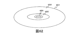
本実施形態のDVD装置3904は、図42に示すように書き込みを行う光ディスク媒体の一部4202をスクランブルを行って書き込む領域、書き込みを行う光ディスク媒体の一部4203をスクランブルを行わないで書き込む領域、として扱い、どのトラックからどのトラックがスクランブルを行って書き込む領域かという情報、またはどのトラックからどのトラックがスクランブルを行わないで書き込む領域かという情報をトラック4201に格納している。
【0122】
本情報は、実施形態2で示したスクランブルモード情報2902、2903、2904、2905と同様に、複数箇所書き込み、強力なECCなどを用いて信頼性を高めることができる。本実施形態のDVD装置3904は、電源ON時、またはディスク媒体交換時、図44に示すようにスクランブル対応領域を示すメッセージ(どのトラックからどのトラックがスクランブルを行って書き込む領域かという情報、またはどのトラックからどのトラックがスクランブルを行わないで書き込む領域かという情報)を、ホストコンピュータに送信する(ステップ4301)。ホストコンピュータは書き換えの特に多いFATデータ、またはアプリケーションの性質上書き換え回数の特に多いデータをスクランブルを行って書き込む領域に書き込む。ホストコンピュータはステップ4301で得たスクランブル対応領域を示すメッセージを用いて、スクランブル対応の論理セクタナンバまたは物理セクタナンバを算出し、FATデータなど特に書き換えの多いデータを当該スクランブルを行って書き込む領域のセクタに割り振り、書き込みコマンドを発行して書き込みを行う。本第9の実施形態に示したように、FATや特に書き込みの頻繁に発生する領域をスクランブルして格納することにより、書き込みが頻繁に起こるFATデータを保護することができる。
【0123】
次に第10の実施形態について、図39、図43を用いて説明する。第10の実施形態におけるDVD装置のブロック図は、図39で示される。ただし、本第10の実施形態におけるDVD装置3904は、第9の実施形態におけるDVD装置同様、オブジェクトコマンド対応の光ディスクではなく、ファイル管理はホストコンピュータにて行い、書き込みコマンドでホストコンピュータにより指定された論理ブロックアドレス、または物理ブロックアドレスなどのアドレスに書き込みを行うDVD装置である。
【0124】
本実施形態のDVD装置3904は、本実施形態の光ディスク媒体は、第2の実施例同様、スクランブルに対応しているかどうかを示すスクランブルモード情報2902、2903、2904、2905が記録されている。電源ON時、またはディスク媒体交換時、図43に示すように、DVD装置3904は、光ディスク媒体からスクランブルモード情報2902、2903、2904、2905を読み出し、スクランブル対応光ディスクであることを示すメッセージをホストコンピュータに送信する(ステップ4301)。
【0125】
ホストコンピュータは、今書き込んでいる光ディスクがスクランブル対応光ディスクであるとき、FATデータなど特に書き換えの多いデータや、アプリケーションで特に書き換えが多くなることがわかっているデータを書き込むとき、データをランダムシードスクランブルして書き込むようにDVD装置に対して指示を出す。
【0126】
具体的には、ホストコンピュータがDVD装置に対して出すコマンドバイト中の決められた1ビットにより、ランダムシードスクランブルをするか、しないかを指定する。DVD装置3904は、コマンドバイト中の前記決められた1ビットがスクランブルをすることを示すものであれば、ランダムシードスクランブルON/OFFを示す信号線4507をONに制御し、データをスクランブルして指定されたアドレスに書き込みを行う。DVD装置3904は、コマンドバイト中の前記決められた1ビットがスクランブルをしないことを示すものであれば、ランダムシードスクランブルON/OFFを示す信号線4507をOFFに制御し、データをランダムシードスクランブルしないで指定されたアドレスに書き込みを行う。本第10の実施形態に示したように、FATや特に書き込みの頻繁に発生する領域をスクランブルして格納することにより、書き込みが頻繁に起こるFATデータを保護することができる。なお、ホストコンピュータがDVD装置に対してランダムシードスクランブルをするか、しないかを指定する方法は、前記コマンドバイト中の1ビットを使う方法のほかに、メッセージバイトとして他に送信する方法や、ホストがDVD装置内のインターフェイス部にある前もって決められた特定のレジスタの1ビットに特定の値を書き込む方法などがある。コマンドバイト中に空きビットがない場合には、これらの方法が有効である。特にSCSIなどのインターフェイスでは、前記メッセージバイト中の1ビットとして他に送信する方法が、ATAインターフェイスでは前もって決められた特定のレジスタの1ビットに特定の値を書き込む方法などが有効であると考えられる。
【0127】
次に第11の実施形態について図38を参照して説明する。本実施形態のDVD装置も図39で示される。図38は本第11の実施形態の光ディスク媒体301を示す図であり、光ディスク媒体301の一部をカットして、断面を見せた図である。光ディスク301はn層の記録層を持っており、表面から3801、3802となり、最も表面から遠い層が3803である。一般に表面から最も遠い層3803は、それより奥に光を透過させる必要がないので、光を反射させる反射層として金属を使うことができるが、それよりも表面に近い層3801、3802は、それより奥に光を透過させる必要があるので、反射層として金属を使うことができず、流動現象が起こりやすくオーバーライトによる媒体劣化が起こりやすいという特徴がある。したがって、本実施形態においては、表面から1層目の記録層3801、2層目の記録層3802、・・・、表面からn−1層目の記録層は媒体劣化を防ぐためのランダムシードスクランブルを行って媒体上にデータを記録し、表面から1番奥のn層目の記録層3803はランダムシードスクランブルを行わずに記録するものである。各層の最内周のトラック3804には、第2の実施例同様、各層がランダムシードスクランブルに対応しているかを示すスクランブルモード情報2902、2903、2904、2905が記録されている。
【0128】
光ディスクドライブは、電源ON時、または、光ディスク媒体の交換時、または、アクセスしている層の移動時に、最内周にかかれている各層のスクランブルモード情報を読み出して、その値をマイコン内に保持し、書き込み時にランダムシードスクランブルを行ってから書き込むか、ランダムシードスクランブルを行わずに書き込むかを制御する。このようにすることにより、ランダムシードスクランブルに対応していないDVD装置においては第n層目3803だけの1層の光ディスクとして取り扱うことが可能となり、ランダムシードスクランブルに対応しているDVD装置においては、n層の記録層を備え、すべての層の書き換え回数を一定以上保証できる光ディスクとして取り扱うことができ、1層のみの光ディスク倍に比べ、n倍の記録容量を持った光ディスクとして取り扱われる。このような光ディスクは、たとえば、記録層3803に画像、音声などの基礎データ、記録層3801、3802に補間データなどを入れることにより、ランダムシードスクランブルに対応していないDVD装置においては、画質、音質のあまりよくないデータのみが再生でき、ランダムシードスクランブルに対応しているDVD装置においては、高品質の画質、音質を再生できる光ディスク媒体として使用することもできる。
【0129】
本発明は、上述の実施の形態に限定されるものではなく、適用分野に関わらず、要旨を逸脱しない範囲で変更し実施し得ることは述べるまでもない。
【0130】
【発明の効果】
本発明によれば、ディスク上に記録すべき元データに、任意のシードデータを付加し、データのスクランブルを行うことにより、媒体劣化を防ぐことができるランダムシードスクランブルを次世代光ディスクに適用することができる。さらに、ランダムシードスクランブルが適用されているセクタとそうでないセクタが1枚の光ディスク上で混在している場合でも再生できる。またランダムシードスクランブルを採用していない装置でも、ランダムシードスクランブルを採用していない装置でも、同じ光ディスクに読み書きを行うことができる。
【図面の簡単な説明】
【図1】本発明のスクランブル回路を示す図である。
【図2】本発明のデスクランブル回路を示す図である。
【図3】本発明の第1の実施形態の概略ブロック図である。
【図4】本発明の第1の実施形態のスクランブル回路の詳細ブロック図である。
【図5】本発明の第1の実施形態のM系列生成器の詳細回路図である。
【図6】本発明の第1の実施形態の2次スクランブル回路の詳細回路図である。
【図7】本発明の第1の実施形態のデスクランブル回路の詳細ブロック図である。
【図8】本発明の第1の実施形態の2次デスクランブル回路の詳細回路図である。
【図9】本発明の第1の実施形態の概念図である。
【図10】次世代光ディスクの記録フォーマット図である。
【図11】本発明の第2の実施形態のデータセクタフォーマット図である。
【図12】本発明の第2の実施形態の記録フォーマット図である。
【図13】本発明の第4の実施形態の記録フォーマットである。
【図14】本発明の第2の実施形態のシステムブロック図である。
【図15】本発明の第2の実施形態の記録時の処理フローチャートである。
【図16】本発明の第2の実施形態の再生時の処理フローチャートである。
【図17】本発明の第4の実施形態の概略ブロック図である。
【図18】本発明の第4の実施形態の光ディスクシステムのブロック図である。
【図19】本発明の第2の実施形態のシード生成器の詳細ブロック図である。
【図20】本発明の第2の実施形態のスクランブル回路のブロック図である。
【図21】本発明の第2の実施形態のデスクランブル回路のブロック図である。
【図22】本発明の第3の実施形態の記録フォーマットを示す図である。
【図23】本発明の第3の実施形態の書き換え回数記録メモリのブロック図である。
【図24】本発明の第3の実施形態の記録時の処理フローチャートの一部である。
【図25】本発明の第3の実施形態の再生時の処理フローチャートである。
【図26】本発明の第5の実施形態の光ディスクシステムのブロック図である。
【図27】本発明の第6の実施形態の光ディスクシステムのブロック図である。
【図28】本発明の第3の実施形態の光ディスクシステムのブロック図である。
【図29】本発明の第2の実施形態の光ディスク媒体の模式図である。
【図30】本発明の第3の実施形態の光ディスク媒体の模式図である。
【図31】本発明の第2の実施形態の一部書き換え時の処理フローチャートである。
【図32】本発明の第3の実施形態の電源ON時および光ディスク挿入時の処理フローチャートである。
【図33】本発明の第3の実施形態の記録時の処理フローチャートの一部である。
【図34】本発明の第3の実施形態の記録時の処理フローチャートの一部である。
【図35】本発明の第7の実施形態の光ディスクシステムのブロック図である。
【図36】本発明の第3の実施形態の電源OFF時および光ディスク取り出し時の処理フローチャートの一部である。
【図37】本発明の第8の実施形態の光ディスク媒体の模式図である。
【図38】本発明の第11の実施形態の光ディスク媒体の模式図である。
【図39】本発明の第8から第11の実施形態の光ディスクシステムのブロック図である。
【図40】本発明の第8から第11の実施形態のシード生成器の詳細ブロック図である。
【図41】本発明の第8の実施形態の記録時の処理を示すフローチャートである。
【図42】本発明の第9の実施形態の光ディスク媒体の模式図である。
【図43】本発明の第10の実施形態の電源ON時またはディスク交換時の処理を示すフローチャートである。
【図44】本発明の第9の実施形態の電源ON時またはディスク交換時の処理を示すフローチャートである。
【図45】本発明の第8から第11の実施形態のスクランブル器の詳細ブロック図である。
【図46】本発明の第8から第11の実施形態のデスクランブル器の詳細ブロック図である。
【符号の説明】
101〜104:1ビットレジスタ
105〜109:排他的論理和回路
201〜204:1ビットレジスタ
205〜209:排他的論理和回路
301:光ディスク
302:光ヘッド
303:記録再生アンプ
304:データ再生回路
305:ラン長制限符号化回路
306:ラン長制限符号復号回路
307:エラー訂正符号化回路
308:エラー訂正回路
309:スクランブル回路
310:デスクランブル回路
311:ホストI/F
401:M系列生成器
402:排他的論理和回路
403:ランダムシードスクランブル器
404:ランダムデータ付加回路
405:2次スクランブル回路
501:排他的論理和回路
502〜516:1ビットレジスタ
601〜604:排他的論理和回路
605〜612:1ビットレジスタ
701:M系列生成器
702:排他的論理和回路
703:ランダムシードデスクランブル器
704:2次デスクランブル回路
705:ランダムデータ削除回路
801〜808:1ビットレジスタ
809〜812:排他的論理和回路[0001]
BACKGROUND OF THE INVENTION
The present invention relates to an optical disc apparatus such as a DVD, and more particularly to a data scrambling method when data is recorded on a medium in the optical disc apparatus.
[0002]
[Prior art]
In general, in a rewritable optical disc such as a DVD-RAM, data is written by generating a recording mark on the track of the disc by the power of light. In addition, data is read using the difference in reflectance of light between the recording mark and other locations. In DVD-RAM, grooves called grooves are formed on a disk, and the density is increased by writing data in both grooves (lands) and non-groove portions (grooves).
[0003]
In a recording / reproducing apparatus using a disk-type recording medium, control for accurately positioning the head on a track is called tracking. In a DVD-RAM, lands and grooves are formed with minute vibrations called wobbles, and tracking is performed using this. However, if the same data is written in adjacent tracks, the tracking signal becomes weak, and there is a problem that tracking is easily lost. In a DVD that handles images, sounds, and the like, it often happens that the same data such as a silent part is written in large quantities. In order to solve this problem, various measures have been taken so that even if a large amount of the same data is written by the user, the write data of adjacent tracks is not the same.
[0004]
For example, as disclosed in Japanese Patent Application Laid-Open No. Hei 6-274485, there is a method of changing the start of a sector from a mark or a non-mark for each track. Further, as described in STANDARD-ECMA-272, in DVD-RAM, an M series (random series) is generated using ID information of each frame as an initial value (seed), and added to user data. Then, the method of writing on the disk was taken. Such randomization of data is generally called scrambling.
[0005]
On the other hand, in the field of optical communication, a method called guided scrambling has been used for the purpose of creating a run length limited code having a flat frequency characteristic suitable for optical communication. This is close to the desired characteristics from the data created by randomizing the data by adding data with a sufficiently large space at the beginning of the data for which the run length limit code is to be created. One thing to choose. Such a technique is described in detail, for example, in “CODES FOR MASS DATA STORAGE SYSTEMS” KAS IMMINK, SHANNON FOUNDATION PUBLISHER, 1999. In the paper, “POLYNOMIALS FOR GUIDED SCRAMBLING LINE CODE”, IEEE JOURNAL ON SELECTED AREAS IN COMMUNICATIONS, Vol. 13, NO. 3, APRIL, 1995, etc.
[0006]
In recent years, a high-density optical disk using a blue-violet laser has been proposed. For example, “OPTICAL DISC SYSTEM FOR DIGITAL VIDEO RECORDING”, TATSUYA NARAHARA JPN. J. APPL. PHYS. VOL. 39 (2000) PP. 912-919
[0007]
FIG. 10 shows an optical disk formatting method described in the paper. User data is error correction encoded in units of 64 Kbytes and written on a disk medium. An optical disk is read and written in units of 2048 bytes even in a current DVD-RAM, and this is called a logical sector. The input user data is added with a 4-byte error check code EDC to become 2052 bytes. The logical sectors to which the EDC is added are grouped into 8 sectors and divided into 76 by 216 bytes. Each is encoded into a [248, 216, 33] Lead Solomon code, and 8 sectors are grouped together and arranged in the area (A) 1001 (38 bytes × 496 bytes) indicated by shading in FIG. This 38-byte × 496-byte area is called LDC. Similarly, the areas of (B) 1002, (C) 1003, and (D) 1004 are filled together by 8 sectors. Hereinafter, the ReedSolomon code is referred to as an RS code.
[0008]
Next, the address of 8 × 4 = 32 sectors, copy protection information, alternative sector information, etc. are divided into 30 bytes and encoded into 24 [62, 30, 33] RS codes. This is written eight by eight in the three
[0009]
[Problems to be solved by the invention]
By the way, in the optical disk using the next-generation high-density format introduced in the prior art, if the same data is written many times in the same physical location (sector) on the optical disk medium, the medium changes in quality and new data is written. There was a problem that the previous data remained and it appeared as noise. Further, since an optical disk is a replaceable medium, compatibility is important, and when a new technology is introduced, it is necessary to be able to easily read and write even when using an optical disc medium that does not introduce a conventional new technology.
[0010]
[Means for Solving the Problems]
In the scramble method according to the present invention, data is scrambled using an arbitrary seed on the next-generation high-density optical disk introduced in the prior art to solve the above problem. Preferably, arbitrary seed data for randomization is added to the original data to be recorded on the disc. More preferably, additional information such as a sector number and copy protection is further added to the original data to be recorded on the disc, and the address is scrambled together. The randomized data, additional information, and seed data are encoded into an error correction code. Data is stored in the LDC area, and additional information and seed are stored in the BIS area. According to the scramble method of the present invention, 1-bit randomized data is determined by an operation using 1-bit original data or seed data and a plurality of bits of randomized data in the past. According to another aspect of the present invention, a descrambling method that does not require seed data is provided. Specifically, at the time of data reproduction, 1-bit randomization cancellation data is determined by calculation using a plurality of bits of randomized data. Further, according to another aspect of the present invention, even when a randomized area and a non-randomized area coexist on a single disk, a disk that supports randomization or a disk that does not Read and write on the same device without problems. Specifically, with respect to reading, an error detection code or position information of data is detected, and when there is an error, descrambling is performed assuming that the data is scrambled. As for writing,
An area for storing discrimination information is provided in the disc. In addition, an area to be written without being scrambled and an area to be scrambled and written for accessing an optical disk medium by an apparatus that does not support scrambling are provided.
[0011]
DETAILED DESCRIPTION OF THE INVENTION
Hereinafter, the first embodiment of the present invention will be described with reference to FIGS. FIG. 3 is a schematic block diagram showing the configuration of the optical disc apparatus of the present embodiment. The embodiment described below does not limit the present invention, and the optical disk apparatus of the present invention is not limited to a storage device used in a computer system as in this embodiment, but also a stationary image and sound connected to a television. It may be used as a recording / reproducing apparatus such as a recording / reproducing apparatus, a portable video camera, or a portable audio reproducing apparatus.
[0012]
In FIG. 3, a host interface (host I / F) 311 controls data transfer between an optical disk device and a host computer such as a personal computer (not shown). The
[0013]
The electric signal is appropriately amplified by the recording / reproducing
[0014]
The
[0015]
[Expression 1]
The sequence generated by the
[0017]
In the
[0018]
FIG. 6 is a detailed circuit diagram of the
[0019]
[Expression 2]
Here, bi is i-th bit data before entering the secondary scramble circuit, and Ci-j is j-bit data before the i-th data outputted from the secondary scramble circuit. As can be seen from this equation, Ci is generated from 1-bit pre-scrambled data and multi-bit past-scrambled data. Thus, the data is scrambled and then sent to the error
[0021]
Next, the
[0022]
Next, the operation of the
[0023]
[Equation 3]
Here, bi is descrambled i-th user data, and ci-j is i-bit j-bit data input from the
[0025]
Next, as shown in FIG. 9, the random
[0026]
The M-
[0027]
In this embodiment, the scramble circuit is configured using a shift register that performs bit shift, but this may be realized by an equivalent circuit that operates in units of bytes.
In this embodiment, an 8-bit primitive polynomial is used.
[0028]
[Expression 4]
Random seed scramble was performed using, but any polynomial can be used here.
[0030]
[Equation 5]
On the other hand, the scramble circuit can be realized in FIG. 1, and the descramble circuit in FIG. If a primitive polynomial is used as a polynomial, a longer period can be obtained, so that a more random sequence can be obtained. Where a k Is 1 or 0. When 1, the signal line is connected, and when 0, the signal line is not connected. In this embodiment, an 8-bit primitive polynomial is used.
[0032]
[Formula 6]
It can also be expressed as In this case, the general form of the polynomial
[0034]
[Expression 7]
On the other hand, the scramble circuit can be realized in FIG. 1, and the descramble circuit in FIG. Here, ai is 1 or 0. When it is 1, the signal line is connected, and when it is 0, the signal line is not connected. The relationship between
[0036]
In the present embodiment, the
[0037]
Next, as a second embodiment, the case where the random seed scramble described in the first embodiment is applied to the next-generation DVD format will be described in more detail. FIG. 14 is a schematic block diagram of a DVD device according to the second embodiment.
[0038]
This scrambler is the scrambler shown in FIG. 20, and includes the
[0039]
FIG. 19 is a diagram illustrating a
[0040]
The operation of the DVD device shown in FIG. 14 will be described below. First, the recording operation will be described with reference to the optical disc shown in FIG. 29, the format shown in FIG. 11, and the processing procedure shown in FIG. In the optical disc shown in FIG. 29, scramble mode information indicating whether or not the present optical disc supports random seed scramble is written in the innermost track 2901. In order to provide the scramble mode information with reliability, the same information as 2902, 2903, 2904, and 2905 is written in four places. Further, as shown in the present embodiment, by writing in the innermost circumference, the innermost circumference is hardly damaged, so that the data reliability can be kept high. This scramble mode information is read into the optical disk apparatus when the optical disk apparatus is powered on or inserted, and stored in the
[0041]
Also, it may be divided into a plurality of tracks such as the innermost circumference and the middle circumference. In this case, it takes time to read out the scramble mode information, but the scramble mode information can be stored more reliably. In this embodiment, the number of scramble mode information writing positions is four, but it may be more. Even in this case, the scramble mode information can be stored with higher reliability. Furthermore, in order to write the scramble mode information with high reliability, it can be written with a strong error correction code. Further, when the scramble mode information is written at an odd number, it is always determined by majority decision, so that there is an advantage that the processing becomes easy. According to the present invention, it is possible to provide a disk having the above characteristics and an apparatus for recording on the disk.
[0042]
First,
[0043]
If not, the
[0044]
Next, the error
[0045]
Next, the
[0046]
The run-length limited code sequence is written to the
[0047]
In the case of an AV system in which speed is more important than reliability,
[0048]
Next, a processing procedure during reproduction will be described with reference to FIG. During reproduction, data is read by the
[0049]
The
[0050]
Thereafter, it is confirmed that there is no error in the
[0051]
In addition, since random seed scramble causes error propagation, it is desirable to perform scramble processing on the user side rather than error correction coding in consideration of relieving data even if error correction is impossible. Further, as shown in the present embodiment, it is desirable that the additional information such as an ID corresponding to the user data is descrambled before the user data. By doing in this way, since ID can be confirmed early, re-reading when ID is incorrect can be performed quickly. Also, as shown in this embodiment, the ID is confirmed before data scrambling, and if the desired ID is obtained there, the data is reproduced without descrambling, and the desired ID is not obtained. The ID is confirmed after descrambling, and when the desired ID is obtained, the data is also descrambled and reproduced so that the disc recorded using random seed scramble is also recorded without using it. You can play the disc without worrying. In addition, when this method is used, even if a scrambled ECC block and a non-scrambled ECC block are mixed in one disk, not a disk unit, playback can be performed without concern. According to the present invention, it is possible to provide the disk and an apparatus for reproducing the disk.
[0052]
Further, in this embodiment, the determination is made only with the EDC check result of one logical sector. However, when all the EDC check results for a plurality of logical sectors or one ECC block are OK, the data is not scrambled. You may judge. In this case, the probability of a determination error due to erroneous detection of EDC can be reduced.
[0053]
Next, a processing procedure when only a part of the sectors in the ECC block 64 KB is rewritten will be described with reference to FIG. First,
[0054]
The values of the 1-
[0055]
This completes the data for one ECC block to be written. Next, the
[0056]
Next, the error
[0057]
Next, the
[0058]
In other words, the processing is repeated from
[0059]
Next, a third embodiment will be described with reference to FIGS. FIG. 30 shows an
[0060]
FIG. 28 is a schematic block diagram of a DVD device according to the third embodiment.
[0061]
As shown in FIG. 23, the
[0062]
Next, in the third embodiment, re-scramble is performed using the second seed in order to obtain a preferable sequence of run length limit codes. When a re-scramble seed is requested,
[0063]
The operation in the optical disk apparatus shown in FIG. 28 will be described below. First, the operation when the power is turned on or when the optical disk is inserted will be described with reference to FIG. First, when the optical disk device is powered on (step 3201), the optical disk device 2801 checks whether the
[0064]
If the ID is in the rewrite count recording area, error correction in the LDC area is performed (step 3209), and error detection by EDC is performed (step 3210). If no error is detected by EDC, the inserted optical disk does not support random seed scrambling with the number of rewrites as part of the seed, so
[0065]
Next, the operation during recording will be described with reference to the format shown in FIG. 22 and the processing procedures during recording shown in FIGS. 33, 34, and 24. FIG.
[0066]
First, as shown in FIG. 33, when information about a sector to be written is given from the
[0067]
Thereafter, whether the data has been normally written on the optical disk, or the written data is read and compared with the data on the RAM (step 2408). When data for one ECC block is normally recorded on the
[0068]
When the
[0069]
First, the case where the first two physical blocks are processed will be described. The first seed consisting of the lower 7 bits of the number of rewrites added by “1” and the output of the 1-
[0070]
Next, the second seed in which only the lower 1 bit is inverted with respect to the first seed is selected as one of the
[0071]
Here, as a method of selecting a sequence with good characteristics, (1) a sequence having a maximum mark and a small maximum space is selected. (2) Select a low-frequency component of the code. (3) Various methods can be considered, such as selecting the smallest mark and the smallest space with a low occurrence frequency.
[0072]
Next, when the selected sequence is generated from the second seed, the seed and the random seed scrambled sequence are moved from the area B2803 on the
[0073]
However, if recording fails for some reason during the recording of data, the same data is written to the same location, and the medium deteriorates. Therefore, in this case, the seed is changed and re-scrambled to rewrite the data. That is, the process shown in FIG. 34 is performed. First, the number of rewrites of the corresponding ECC block stored in the
[0074]
Next, the shift register of the random seed scramble circuit is set with the first seed (step 3406). Next, the descrambled user data is randomly seed scrambled. At this time, the random seed scramble is performed in the order of the arrow 1009 of the recording / reproducing order shown in FIG. 22 (step 3407). If the physical block being processed is the seventh, eighth sector, or the fifteenth or sixteenth sector (step 3408), since the user data is only partway, it is encoded into [248, 216, 33] RS code (step 3409). ), It writes in the area A2802 on the RAM 1402 (step 3410). A synchronization signal is added (step 3411), and run length limited encoding is performed (step 3412). Next, the second seed in which only the lower 1 bit is inverted with respect to the first seed is selected as one of the
[0075]
Next, the data in the BIS area in the first two physical blocks currently processed is [62, 30, 33] RS encoded by the error correction encoding circuit 307 (step 3414). Next, the shift register of the random seed scramble circuit is set with the second seed (step 3415). The user data obtained in step 3405 is randomly seed scrambled. At this time, random seed scramble is performed in the order of arrows in the recording / playback order shown in FIG. 22 (step 3416). If the physical block being processed is the seventh, eighth or fifteenth, sixteenth sector (step 3417), the user data is only partway, so it is encoded into [248, 216, 33] RS code (step 3418). ), It writes in the area B2803 on the RAM 1402 (step 3419). A synchronization signal is added (step 3420), and run length limited encoding is performed (step 3421). Of the two sequences on the run length restriction code created in steps 3412 and 3421, a sequence having a good property is selected (step 3422), and written to the
[0076]
Next, when the selected sequence is generated from the second seed, the seed and the random seed scrambled sequence are moved from the area B2803 on the
[0077]
Next, the operation during reproduction will be described with reference to the processing procedure of FIG. First, the optical disk device 2801 reads data from the optical disk (step 2501). First, run length limited code decoding is performed (step 2502) and stored in the RAM 1402 (step 2503). Error correction of the BIS area is performed (step 2504), and the ID written in the BIS area is confirmed (step 2505). In the third embodiment, since the BIS area is not scrambled, the descrambling process is not performed. If the ID is the ECC block that is in the read request, error correction of the LDC area is performed (step 2506), and error detection by EDC is performed (step 2507). If no error is detected by EDC, the process proceeds to step 2510. If an error is detected by EDC, the data is descrambled (step 2508), and error detection by EDC is performed again (step 2509). If an error is detected by EDC, the process is repeated from step 2501. If no error is detected by EDC, the added seed, ID information, etc. are deleted (step 2510), EDC is deleted (step 2511), and the decoded user data is output from interface 311 (step 2511). 2512). By controlling in this way, even when a random seed scrambled area and a non-random area are mixed on a single disc, it is possible to easily read out without providing special bits on the format to indicate that area. It can be carried out.
[0078]
Next, operations when the power is turned off and when the optical disk is taken out will be described with reference to the processing procedure shown in FIG. When a power OFF command or an optical disk eject command is generated, the optical disk device 2801 first refers to the information bit 2805 (step 3603), and proceeds to step 3606 if the
[0079]
As shown in the third embodiment, after a plurality of RLL sequences are generated, a technique for producing a disk having a sequence having a good characteristic by selecting one having a good sequence characteristic is particularly a ROM disk. It is effective in the creation device. The ROM disk creation device can also be configured in the same manner as in the third embodiment.
[0080]
Further, according to the third embodiment, a run length code sequence with better properties can be obtained by selecting from a plurality of sequences.
[0081]
Next, a fourth embodiment will be described with reference to FIGS. FIG. 18 is a schematic block diagram of an optical disc apparatus 2801 shown in the fourth embodiment.
[0082]
[0083]
Hereinafter, the operation of the optical disc apparatus shown in FIG. 18 will be described with reference to FIG. First, at the time of recording, additional information necessary for recording, such as an ID, is added to the user data input from the
[0084]
Thereafter, user data is written according to the format of FIG. Further, the seed storage location may be embedded in an unused area among the
[0085]
By placing random seed scrambling on the medium side of the error correction circuit as shown in the present embodiment, the error correction encoding process can be omitted in the rewriting process, and therefore the rewriting process can be executed at high speed.
[0086]
Next, a fifth embodiment will be described with reference to FIG. In the fifth, sixth, and seventh embodiments, a method of applying random seed scrambling to an optical disc apparatus controlled by an existing optical disc control LSI incorporating an error correction encoding circuit and the like will be described. First, in the fifth embodiment, a scramble LSI 2605 that performs random seed scramble processing is placed closer to the host interface than the optical
[0087]
Next, the operation during recording will be described. First, when information such as the data size and recording location ID of the sector to be written is given from the
[0088]
If the logical sector is data to be written in a different ECC block than the first logical sector, the
[0089]
Next, 2048 bytes (one logical sector) of
[0090]
Next, a processing procedure during reproduction will be described. During reproduction, data is read by the
[0091]
By adopting the configuration of the fifth embodiment as described above, since the scramble is released after the error correction process is completed, the error correction capability does not deteriorate due to the error propagation of the random seed scramble. In the fifth embodiment, in each ECC block, each logical sector is subjected to random seed scramble processing using the same seed. However, a method of continuously scrambling one ECC block 64 Kbytes is also conceivable. A method of performing random seed scramble processing using different seeds for each logical sector is conceivable. In this case, it is necessary to secure a 32-byte area as an area for storing the first scrambled byte in the BIS area.
[0092]
In addition, since random seed scramble causes error propagation, it is desirable to perform scramble processing on the user side rather than error correction coding in consideration of relieving data even if error correction is impossible.
[0093]
Next, a sixth embodiment will be described with reference to FIG. In the sixth embodiment, a scramble LSI 2701 that performs random seed scramble processing is placed closer to the optical disc medium than the optical
[0094]
Next, the operation during recording will be described. First, when information about a sector to be written is given from the
[0095]
Next, 2048 bytes (one logical sector) of
[0096]
Next, the
[0097]
Next, a processing procedure during reproduction will be described. During reproduction, data is read by the
[0098]
Here, if the ID is the ID of the ECC block or sector desired to be read, error correction processing of the LDC area is performed, the
[0099]
Next, a seventh embodiment will be described with reference to FIG. In the seventh embodiment, the random seed scramble process is processed by the
[0100]
Next, the operation during recording will be described. First, when information about a sector to be written is given from the
[0101]
[Equation 8]
Here, k indicates the kth seed generation. n is an appropriate 256 and a sparse number. The 1-byte seed generated by the
[0103]
Next, 2048 bytes (one logical sector) of
[0104]
[Expression 2]
In this calculation, bi is the i-th user data to be read. The calculation is performed by reading data bit by bit from the beginning of user data on the
[0106]
When the scramble by the
[0107]
Next, a processing procedure during reproduction will be described. During reproduction, data is read by the
[0108]
Here, if the ID is the ID of the ECC block or sector desired to be read, error correction processing in the LDC area is performed. Next, the
[0109]
[Equation 3]
The 1-byte seed is used as an initial value from c-7 to c0 in calculating
[0111]
After completion of the scramble, the
[0112]
Next, an eighth embodiment will be described. In general, when an optical disk is used as a computer recording medium, it is said that it is necessary to withstand a larger number of rewrites than when an optical disk is used for audio. This is because the computer performs disk management while frequently rewriting the FAT (File Allocation Table) written in the disk. The area in which the FAT is written is larger than the area in which general data is written. It is said that rewriting more than 10 times occurs. By the way, the
[0113]
FIG. 39 is a schematic block diagram of a DVD device according to the eighth embodiment. 311 performs data input / output control with the host device, and converts a file name and a physical address.
[0114]
A
[0115]
FIG. 40 is a diagram illustrating a
[0116]
Hereinafter, the operation of the DVD apparatus shown in FIG. 39 will be described. First, the recording operation will be described with reference to the optical disc shown in FIG. 37 and the recording processing procedure shown in FIG.
[0117]
First, when the file name and file size to be written are input from the interface 311 (step 4101), the
[0118]
Next, the FAT is updated, and the FAT is written in the
[0119]
As shown in the eighth embodiment, by storing the scrambled FAT, the FAT data frequently written can be protected. In addition, data can be read out by an existing optical disc apparatus that does not support scramble by writing one of the data area and FAT that does not frequently rewrite on the optical disc medium without being scrambled.
[0120]
Next, a ninth embodiment will be described with reference to FIGS. 39, 42, and 44. FIG. A block diagram of a DVD apparatus according to the ninth embodiment is shown in FIG. However, the
[0121]
As shown in FIG. 42, the
[0122]
Similar to the
[0123]
Next, a tenth embodiment will be described with reference to FIGS. 39 and 43. FIG. A block diagram of a DVD device according to the tenth embodiment is shown in FIG. However, the
[0124]
The
[0125]
The host computer randomly scrambles the data when writing the optical disk that is currently being written to a scramble-compatible optical disk, such as FAT data, or data that is especially rewritten, or data that is known to be rewritten by the application. To instruct the DVD device to write.
[0126]
Specifically, whether or not to perform random seed scramble is specified by a predetermined bit in a command byte issued from the host computer to the DVD device. The
[0127]
Next, an eleventh embodiment will be described with reference to FIG. The DVD device of this embodiment is also shown in FIG. FIG. 38 is a diagram showing an
[0128]
The optical disk drive reads the scramble mode information of each layer written on the innermost circumference when the power is turned on, the optical disk medium is changed, or the layer being accessed is moved, and the value is stored in the microcomputer. Then, it is controlled whether writing is performed after random seed scrambling at the time of writing or without performing random seed scrambling. By doing so, a DVD device that does not support random seed scramble can be handled as a single-layer optical disk having only the n-
[0129]
The present invention is not limited to the above-described embodiment, and it goes without saying that the present invention can be modified and implemented without departing from the gist, regardless of the application field.
[0130]
【The invention's effect】
According to the present invention, random seed scramble that can prevent medium deterioration by applying arbitrary seed data to original data to be recorded on a disk and performing data scrambling is applied to a next-generation optical disk. Can do. Furthermore, even if sectors to which random seed scramble is applied and sectors that are not so are mixed on one optical disc, it can be reproduced. Further, a device that does not employ random seed scramble or a device that does not employ random seed scramble can read and write data on the same optical disk.
[Brief description of the drawings]
FIG. 1 shows a scramble circuit of the present invention.
FIG. 2 is a diagram illustrating a descrambling circuit according to the present invention.
FIG. 3 is a schematic block diagram of a first embodiment of the present invention.
FIG. 4 is a detailed block diagram of a scramble circuit according to the first embodiment of the present invention.
FIG. 5 is a detailed circuit diagram of an M-sequence generator according to the first embodiment of this invention.
FIG. 6 is a detailed circuit diagram of a secondary scramble circuit according to the first embodiment of the present invention.
FIG. 7 is a detailed block diagram of a descrambling circuit according to the first embodiment of this invention.
FIG. 8 is a detailed circuit diagram of a secondary descrambling circuit according to the first embodiment of this invention.
FIG. 9 is a conceptual diagram of the first embodiment of the present invention.
FIG. 10 is a recording format diagram of the next generation optical disc.
FIG. 11 is a data sector format diagram of the second embodiment of the present invention;
FIG. 12 is a recording format diagram according to the second embodiment of the present invention.
FIG. 13 shows a recording format according to the fourth embodiment of the present invention.
FIG. 14 is a system block diagram according to a second embodiment of this invention.
FIG. 15 is a processing flowchart at the time of recording according to the second embodiment of the present invention;
FIG. 16 is a processing flowchart at the time of reproduction according to the second embodiment of this invention;
FIG. 17 is a schematic block diagram of a fourth embodiment of the present invention.
FIG. 18 is a block diagram of an optical disc system according to a fourth embodiment of the present invention.
FIG. 19 is a detailed block diagram of a seed generator according to the second embodiment of this invention.
FIG. 20 is a block diagram of a scramble circuit according to a second embodiment of the present invention.
FIG. 21 is a block diagram of a descrambling circuit according to a second embodiment of this invention.
FIG. 22 is a diagram showing a recording format according to a third embodiment of the present invention.
FIG. 23 is a block diagram of a rewrite count recording memory according to a third embodiment of the present invention.
FIG. 24 is a part of a processing flowchart at the time of recording according to the third embodiment of the present invention;
FIG. 25 is a processing flowchart during reproduction according to the third embodiment of this invention;
FIG. 26 is a block diagram of an optical disc system according to a fifth embodiment of the present invention.
FIG. 27 is a block diagram of an optical disc system according to a sixth embodiment of the present invention.
FIG. 28 is a block diagram of an optical disc system according to a third embodiment of the present invention.
FIG. 29 is a schematic diagram of an optical disc medium according to a second embodiment of the present invention.
FIG. 30 is a schematic diagram of an optical disc medium according to a third embodiment of the present invention.
FIG. 31 is a processing flowchart for partial rewriting according to the second embodiment of this invention;
FIG. 32 is a processing flowchart at power-on and when an optical disc is inserted according to the third embodiment of the present invention.
FIG. 33 is a part of a processing flowchart during recording according to the third embodiment of the present invention.
FIG. 34 is a part of a processing flowchart at the time of recording according to the third embodiment of the present invention;
FIG. 35 is a block diagram of an optical disc system according to a seventh embodiment of this invention.
FIG. 36 is a part of a processing flowchart when the power is turned off and the optical disk is ejected according to the third embodiment of the present invention.
FIG. 37 is a schematic diagram of an optical disc medium according to an eighth embodiment of the present invention.
FIG. 38 is a schematic diagram of an optical disc medium according to an eleventh embodiment of the present invention.
FIG. 39 is a block diagram of optical disc systems according to eighth to eleventh embodiments of the present invention.
FIG. 40 is a detailed block diagram of a seed generator according to eighth to eleventh embodiments of the present invention.
FIG. 41 is a flowchart showing processing during recording according to the eighth embodiment of the present invention.
FIG. 42 is a schematic diagram of an optical disc medium according to a ninth embodiment of the present invention.
FIG. 43 is a flowchart showing processing at power-on or disk replacement according to the tenth embodiment of the present invention.
FIG. 44 is a flowchart showing processing at power-on or disk replacement according to the ninth embodiment of the present invention.
FIG. 45 is a detailed block diagram of a scrambler according to the eighth to eleventh embodiments of the present invention.
FIG. 46 is a detailed block diagram of a descrambler according to the eighth to eleventh embodiments of the present invention.
[Explanation of symbols]
101 to 104: 1-bit register
105 to 109: Exclusive OR circuit
201 to 204: 1-bit register
205 to 209: Exclusive OR circuit
301: Optical disc
302: Optical head
303: Recording / playback amplifier
304: Data recovery circuit
305: Run length limited encoding circuit
306: Run length limited code decoding circuit
307: Error correction coding circuit
308: Error correction circuit
309: Scramble circuit
310: Descramble circuit
311: Host I / F
401: M series generator
402: Exclusive OR circuit
403: Random seed scrambler
404: Random data addition circuit
405: Secondary scramble circuit
501: Exclusive OR circuit
502 to 516: 1-bit register
601 to 604: exclusive OR circuit
605 to 612: 1-bit register
701: M series generator
702: Exclusive OR circuit
703: Random seed descrambler
704: Secondary descrambling circuit
705: Random data deletion circuit
801 to 808: 1-bit register
809 to 812: Exclusive OR circuit
Claims (3)
データにシードデータを付加したデータの少なくとも1ビットのデータと、ランダム化された複数ビットのデータとを用いた演算により、少なくとも1ビットのランダム化されたデータを決める演算手段と、該ランダム化されたデータを記録媒体に書き込む書き込み手段とを備え、
書き換えを行うたびに前記シードデータは異なる値を用いて、かつ前記シードデータの一部にセクタ番号の一部又はトラック番号が含まれることとし、
さらに、第1のスクランブルしないで書き込むファイル管理情報と第2のスクランブルして書き込むファイル管理情報を生成するファイル管理情報生成手段と、
データ書き込み時には、同時に前記第1と第2のファイル管理情報を更新する書き込み手段と、
データ読み出し時には、前記第1のファイル情報のみをもちいてデータを読み出し、
第1のファイル情報にエラーが発生した場合には、第2のファイル管理情報からファイル管理情報を読み出す読み出し手段と、
前記第1のファイル管理情報が格納されていたのとは別の領域に、第1のファイル管理情報格納領域を作成するファイル管理情報格納領域生成手段を備えることを特徴とする記録再生装置。Add seed data to randomize the data,
An arithmetic means for determining randomized data of at least one bit by an arithmetic operation using at least one bit of data obtained by adding seed data to the data and randomized multi-bit data; and the randomized Writing means for writing the recorded data to a recording medium,
Each time rewriting, the seed data uses a different value, and a part of the seed data includes a part of a sector number or a track number,
Further, file management information generating means for generating file management information to be written without being scrambled first and file management information to be written after being scrambled second, and
At the time of data writing, writing means for simultaneously updating the first and second file management information,
At the time of data reading, data is read using only the first file information,
When an error occurs in the first file information, reading means for reading the file management information from the second file management information,
A recording / reproducing apparatus comprising: file management information storage area generating means for creating a first file management information storage area in an area different from the area where the first file management information is stored.
データにシードデータを付加したデータの少なくとも1ビットのデータと、ランダム化された複数ビットのデータとを用いた演算により、少なくとも1ビットのランダム化されたデータを決め、
書き換えを行うたびに前記シードデータは異なる値を用いて記録される記録媒体から前記データを再生する再生装置であって、
複数ビットのランダム化されたデータを用いた演算により1ビットのランダム化解除データを求める演算手段を備え、
前記データは、少なくともIDとユーザデータを含み、
前記演算手段を使わずにデータを再生し、再生したデータのIDが読み出しを希望するIDであるかを判断する判断手段を備え、再生したデータのIDが読み出しを希望するIDであった場合にはそのまま再生を行い、再生したデータのIDが読み出しを希望するIDでない場合には、前記演算手段を用いてデータを再生することを特徴とする再生装置。Add seed data to randomize the data,
Determine at least 1-bit randomized data by calculation using at least 1-bit data of data with seed data added to the data and randomized multiple-bit data,
Each time the rewriting is performed, the seed data is a reproducing device that reproduces the data from a recording medium recorded using a different value,
Computation means for obtaining 1-bit randomization cancellation data by computation using randomized data of a plurality of bits,
The data includes at least an ID and user data,
When the data is reproduced without using the calculation means, and a judgment means for judging whether the ID of the reproduced data is an ID desired to be read is provided, and the ID of the reproduced data is an ID desired to be read. Is reproduced as it is, and when the ID of the reproduced data is not the ID desired to be read, the reproducing device reproduces the data using the arithmetic means.
データにシードデータを付加したデータの少なくとも1ビットのデータと、過去のランダム化された複数ビットのデータとを用いた演算により、少なくとも1ビットのランダム化されたデータを決め、
書き換えを行うたびに前記シードデータは異なる値を用いて記録されている記録媒体から前記データを再生する再生装置であって、
複数ビットのランダム化されたデータを用いた演算により1ビットのランダム化解除データを求める演算手段を備え、
前記データは、少なくともユーザデータとエラー検出符号を含み、
前記演算手段を用いずにデータを再生し、再生したデータのエラーをエラー検出符号を用いて検出するエラー検出手段を備え、エラーが検出されない場合にはそのまま再生を行い、エラーが検出された場合には、前記演算手段を用いてデータを再生することを特徴とする再生装置。Add seed data to randomize the data,
At least 1-bit random data is determined by calculation using at least 1-bit data of data obtained by adding seed data to data and past randomized multiple-bit data,
Each time the rewriting is performed, the seed data is a reproducing device that reproduces the data from a recording medium recorded using a different value,
Computation means for obtaining 1-bit randomization cancellation data by computation using randomized data of a plurality of bits,
The data includes at least user data and an error detection code,
When data is reproduced without using the calculation means, and error detection means for detecting an error in the reproduced data using an error detection code is provided. The reproduction apparatus is characterized in that data is reproduced using the arithmetic means.
Priority Applications (3)
| Application Number | Priority Date | Filing Date | Title |
|---|---|---|---|
| JP2001387285A JP4016652B2 (en) | 2001-12-13 | 2001-12-20 | Recording / playback device, playback device. |
| US10/316,875 US20030135798A1 (en) | 2001-12-13 | 2002-12-12 | Optical disk device and data randomizing method for optical disk device |
| US11/455,630 US20060248427A1 (en) | 2001-12-13 | 2006-06-20 | Optical disk device and data randomizing method for optical disk drive |
Applications Claiming Priority (3)
| Application Number | Priority Date | Filing Date | Title |
|---|---|---|---|
| JP2001380332 | 2001-12-13 | ||
| JP2001-380332 | 2001-12-13 | ||
| JP2001387285A JP4016652B2 (en) | 2001-12-13 | 2001-12-20 | Recording / playback device, playback device. |
Publications (3)
| Publication Number | Publication Date |
|---|---|
| JP2003242728A JP2003242728A (en) | 2003-08-29 |
| JP2003242728A5 JP2003242728A5 (en) | 2005-07-21 |
| JP4016652B2 true JP4016652B2 (en) | 2007-12-05 |
Family
ID=27790808
Family Applications (1)
| Application Number | Title | Priority Date | Filing Date |
|---|---|---|---|
| JP2001387285A Expired - Fee Related JP4016652B2 (en) | 2001-12-13 | 2001-12-20 | Recording / playback device, playback device. |
Country Status (1)
| Country | Link |
|---|---|
| JP (1) | JP4016652B2 (en) |
Cited By (1)
| Publication number | Priority date | Publication date | Assignee | Title |
|---|---|---|---|---|
| CN102296752B (en) * | 2011-06-09 | 2013-04-10 | 北京工业大学 | Galvanized welded steel wire mesh beam end structure and method for improving ductility of beam end bottom pressure zone |
Families Citing this family (5)
| Publication number | Priority date | Publication date | Assignee | Title |
|---|---|---|---|---|
| JP4643978B2 (en) | 2004-12-01 | 2011-03-02 | ルネサスエレクトロニクス株式会社 | Scramble circuit, descramble circuit and method, and disk device |
| JP2006155835A (en) | 2004-12-01 | 2006-06-15 | Nec Electronics Corp | Error detection code adding circuit, error detecting circuit and method, and disk device |
| JP4909824B2 (en) * | 2007-06-29 | 2012-04-04 | 株式会社東芝 | Error correction processing apparatus and error correction processing method |
| JP2009284024A (en) * | 2008-05-19 | 2009-12-03 | Fujitsu Ltd | Frame transmission apparatus, and frame transmission method |
| CN111044738B (en) * | 2019-11-08 | 2023-06-09 | 太原理工大学 | Embedded quantitative detection device based on blue-ray CD driver and detection method thereof |
-
2001
- 2001-12-20 JP JP2001387285A patent/JP4016652B2/en not_active Expired - Fee Related
Cited By (1)
| Publication number | Priority date | Publication date | Assignee | Title |
|---|---|---|---|---|
| CN102296752B (en) * | 2011-06-09 | 2013-04-10 | 北京工业大学 | Galvanized welded steel wire mesh beam end structure and method for improving ductility of beam end bottom pressure zone |
Also Published As
| Publication number | Publication date |
|---|---|
| JP2003242728A (en) | 2003-08-29 |
Similar Documents
| Publication | Publication Date | Title |
|---|---|---|
| US20060248427A1 (en) | Optical disk device and data randomizing method for optical disk drive | |
| US8014248B2 (en) | Recording medium with a linking area including dummy data thereon and apparatus and methods for forming, recording, and reproducing the recording medium | |
| JP3779580B2 (en) | Signal processing method and apparatus, signal reproduction method and apparatus, and recording medium | |
| US6842522B1 (en) | Secure digital video disk and player | |
| KR100707807B1 (en) | Data storing medium, data recording apparatus, data recording method, data reproducing apparatus, and data reproducing method | |
| KR100924049B1 (en) | Recording method, recording apparatus, reproducing method and reproducing apparatus | |
| US20050152235A1 (en) | Data recording method and apparatus | |
| US7594155B2 (en) | Recording and reproducing data to/from a recording medium having a user data area and an information area for storing information about the recording medium | |
| US7155015B2 (en) | Optical disk apparatus and data randomizing method using for optical disk apparatus | |
| JP4016652B2 (en) | Recording / playback device, playback device. | |
| TW543032B (en) | Data recording method, data reproducing method, data recording apparatus and data reproducing apparatus | |
| JP3829724B2 (en) | Recording medium, recording method and apparatus, reproducing apparatus and method, and data discrimination method | |
| US6748079B1 (en) | Method and system for recording data on and reading data from an optical medium | |
| KR101039223B1 (en) | Method and apparatus for copying copy protected optical discs | |
| JP3575461B2 (en) | Recording medium, recording method and apparatus, and reproducing apparatus and method | |
| JP2003242728A5 (en) | ||
| JP5021197B2 (en) | DISC RECORDING MEDIUM AND MANUFACTURING METHOD THEREOF, DISC RECORDING METHOD AND DEVICE, AND DISC REPRODUCING METHOD AND DEVICE | |
| JP2002222524A (en) | Optical disk device, and data randomizing method for the same | |
| JP2005085425A (en) | Information recording processing device, information reproduction processing device, information recording medium, method and computer program | |
| JP2005004837A (en) | Device for recording and playing back recording medium | |
| JP2008159117A (en) | Data recording medium | |
| JP2005038453A (en) | Data recording method and data reproducing method | |
| JP2006197606A (en) | Signal processing method and apparatus, signal reproducing method and apparatus, and recording medium |
Legal Events
| Date | Code | Title | Description |
|---|---|---|---|
| A521 | Written amendment |
Free format text: JAPANESE INTERMEDIATE CODE: A523 Effective date: 20041202 |
|
| A621 | Written request for application examination |
Free format text: JAPANESE INTERMEDIATE CODE: A621 Effective date: 20041202 |
|
| RD01 | Notification of change of attorney |
Free format text: JAPANESE INTERMEDIATE CODE: A7421 Effective date: 20060419 |
|
| A977 | Report on retrieval |
Free format text: JAPANESE INTERMEDIATE CODE: A971007 Effective date: 20070402 |
|
| A131 | Notification of reasons for refusal |
Free format text: JAPANESE INTERMEDIATE CODE: A131 Effective date: 20070515 |
|
| A521 | Written amendment |
Free format text: JAPANESE INTERMEDIATE CODE: A523 Effective date: 20070626 |
|
| TRDD | Decision of grant or rejection written | ||
| A01 | Written decision to grant a patent or to grant a registration (utility model) |
Free format text: JAPANESE INTERMEDIATE CODE: A01 Effective date: 20070828 |
|
| A61 | First payment of annual fees (during grant procedure) |
Free format text: JAPANESE INTERMEDIATE CODE: A61 Effective date: 20070910 |
|
| FPAY | Renewal fee payment (event date is renewal date of database) |
Free format text: PAYMENT UNTIL: 20100928 Year of fee payment: 3 |
|
| LAPS | Cancellation because of no payment of annual fees |