JP4014481B2 - Bonding method and apparatus - Google Patents
Bonding method and apparatus Download PDFInfo
- Publication number
- JP4014481B2 JP4014481B2 JP2002292580A JP2002292580A JP4014481B2 JP 4014481 B2 JP4014481 B2 JP 4014481B2 JP 2002292580 A JP2002292580 A JP 2002292580A JP 2002292580 A JP2002292580 A JP 2002292580A JP 4014481 B2 JP4014481 B2 JP 4014481B2
- Authority
- JP
- Japan
- Prior art keywords
- substrate
- resin
- temperature
- mounting member
- cooling
- Prior art date
- Legal status (The legal status is an assumption and is not a legal conclusion. Google has not performed a legal analysis and makes no representation as to the accuracy of the status listed.)
- Expired - Fee Related
Links
Images


Classifications
-
- H—ELECTRICITY
- H01—ELECTRIC ELEMENTS
- H01L—SEMICONDUCTOR DEVICES NOT COVERED BY CLASS H10
- H01L24/00—Arrangements for connecting or disconnecting semiconductor or solid-state bodies; Methods or apparatus related thereto
- H01L24/80—Methods for connecting semiconductor or other solid state bodies using means for bonding being attached to, or being formed on, the surface to be connected
- H01L24/83—Methods for connecting semiconductor or other solid state bodies using means for bonding being attached to, or being formed on, the surface to be connected using a layer connector
-
- H—ELECTRICITY
- H01—ELECTRIC ELEMENTS
- H01L—SEMICONDUCTOR DEVICES NOT COVERED BY CLASS H10
- H01L24/00—Arrangements for connecting or disconnecting semiconductor or solid-state bodies; Methods or apparatus related thereto
- H01L24/01—Means for bonding being attached to, or being formed on, the surface to be connected, e.g. chip-to-package, die-attach, "first-level" interconnects; Manufacturing methods related thereto
- H01L24/26—Layer connectors, e.g. plate connectors, solder or adhesive layers; Manufacturing methods related thereto
- H01L24/28—Structure, shape, material or disposition of the layer connectors prior to the connecting process
- H01L24/29—Structure, shape, material or disposition of the layer connectors prior to the connecting process of an individual layer connector
-
- H—ELECTRICITY
- H01—ELECTRIC ELEMENTS
- H01L—SEMICONDUCTOR DEVICES NOT COVERED BY CLASS H10
- H01L24/00—Arrangements for connecting or disconnecting semiconductor or solid-state bodies; Methods or apparatus related thereto
- H01L24/74—Apparatus for manufacturing arrangements for connecting or disconnecting semiconductor or solid-state bodies
- H01L24/75—Apparatus for connecting with bump connectors or layer connectors
-
- H—ELECTRICITY
- H01—ELECTRIC ELEMENTS
- H01L—SEMICONDUCTOR DEVICES NOT COVERED BY CLASS H10
- H01L2224/00—Indexing scheme for arrangements for connecting or disconnecting semiconductor or solid-state bodies and methods related thereto as covered by H01L24/00
- H01L2224/01—Means for bonding being attached to, or being formed on, the surface to be connected, e.g. chip-to-package, die-attach, "first-level" interconnects; Manufacturing methods related thereto
- H01L2224/10—Bump connectors; Manufacturing methods related thereto
- H01L2224/15—Structure, shape, material or disposition of the bump connectors after the connecting process
- H01L2224/16—Structure, shape, material or disposition of the bump connectors after the connecting process of an individual bump connector
- H01L2224/161—Disposition
- H01L2224/16151—Disposition the bump connector connecting between a semiconductor or solid-state body and an item not being a semiconductor or solid-state body, e.g. chip-to-substrate, chip-to-passive
- H01L2224/16221—Disposition the bump connector connecting between a semiconductor or solid-state body and an item not being a semiconductor or solid-state body, e.g. chip-to-substrate, chip-to-passive the body and the item being stacked
- H01L2224/16225—Disposition the bump connector connecting between a semiconductor or solid-state body and an item not being a semiconductor or solid-state body, e.g. chip-to-substrate, chip-to-passive the body and the item being stacked the item being non-metallic, e.g. insulating substrate with or without metallisation
-
- H—ELECTRICITY
- H01—ELECTRIC ELEMENTS
- H01L—SEMICONDUCTOR DEVICES NOT COVERED BY CLASS H10
- H01L2224/00—Indexing scheme for arrangements for connecting or disconnecting semiconductor or solid-state bodies and methods related thereto as covered by H01L24/00
- H01L2224/01—Means for bonding being attached to, or being formed on, the surface to be connected, e.g. chip-to-package, die-attach, "first-level" interconnects; Manufacturing methods related thereto
- H01L2224/26—Layer connectors, e.g. plate connectors, solder or adhesive layers; Manufacturing methods related thereto
- H01L2224/28—Structure, shape, material or disposition of the layer connectors prior to the connecting process
- H01L2224/29—Structure, shape, material or disposition of the layer connectors prior to the connecting process of an individual layer connector
- H01L2224/29001—Core members of the layer connector
- H01L2224/29099—Material
- H01L2224/29198—Material with a principal constituent of the material being a combination of two or more materials in the form of a matrix with a filler, i.e. being a hybrid material, e.g. segmented structures, foams
- H01L2224/29298—Fillers
- H01L2224/29399—Coating material
-
- H—ELECTRICITY
- H01—ELECTRIC ELEMENTS
- H01L—SEMICONDUCTOR DEVICES NOT COVERED BY CLASS H10
- H01L2224/00—Indexing scheme for arrangements for connecting or disconnecting semiconductor or solid-state bodies and methods related thereto as covered by H01L24/00
- H01L2224/73—Means for bonding being of different types provided for in two or more of groups H01L2224/10, H01L2224/18, H01L2224/26, H01L2224/34, H01L2224/42, H01L2224/50, H01L2224/63, H01L2224/71
- H01L2224/732—Location after the connecting process
- H01L2224/73201—Location after the connecting process on the same surface
- H01L2224/73203—Bump and layer connectors
- H01L2224/73204—Bump and layer connectors the bump connector being embedded into the layer connector
-
- H—ELECTRICITY
- H01—ELECTRIC ELEMENTS
- H01L—SEMICONDUCTOR DEVICES NOT COVERED BY CLASS H10
- H01L2224/00—Indexing scheme for arrangements for connecting or disconnecting semiconductor or solid-state bodies and methods related thereto as covered by H01L24/00
- H01L2224/80—Methods for connecting semiconductor or other solid state bodies using means for bonding being attached to, or being formed on, the surface to be connected
- H01L2224/83—Methods for connecting semiconductor or other solid state bodies using means for bonding being attached to, or being formed on, the surface to be connected using a layer connector
- H01L2224/8319—Arrangement of the layer connectors prior to mounting
-
- H—ELECTRICITY
- H01—ELECTRIC ELEMENTS
- H01L—SEMICONDUCTOR DEVICES NOT COVERED BY CLASS H10
- H01L2224/00—Indexing scheme for arrangements for connecting or disconnecting semiconductor or solid-state bodies and methods related thereto as covered by H01L24/00
- H01L2224/80—Methods for connecting semiconductor or other solid state bodies using means for bonding being attached to, or being formed on, the surface to be connected
- H01L2224/83—Methods for connecting semiconductor or other solid state bodies using means for bonding being attached to, or being formed on, the surface to be connected using a layer connector
- H01L2224/838—Bonding techniques
-
- H—ELECTRICITY
- H01—ELECTRIC ELEMENTS
- H01L—SEMICONDUCTOR DEVICES NOT COVERED BY CLASS H10
- H01L2924/00—Indexing scheme for arrangements or methods for connecting or disconnecting semiconductor or solid-state bodies as covered by H01L24/00
- H01L2924/01—Chemical elements
- H01L2924/01004—Beryllium [Be]
-
- H—ELECTRICITY
- H01—ELECTRIC ELEMENTS
- H01L—SEMICONDUCTOR DEVICES NOT COVERED BY CLASS H10
- H01L2924/00—Indexing scheme for arrangements or methods for connecting or disconnecting semiconductor or solid-state bodies as covered by H01L24/00
- H01L2924/01—Chemical elements
- H01L2924/01005—Boron [B]
-
- H—ELECTRICITY
- H01—ELECTRIC ELEMENTS
- H01L—SEMICONDUCTOR DEVICES NOT COVERED BY CLASS H10
- H01L2924/00—Indexing scheme for arrangements or methods for connecting or disconnecting semiconductor or solid-state bodies as covered by H01L24/00
- H01L2924/01—Chemical elements
- H01L2924/01006—Carbon [C]
-
- H—ELECTRICITY
- H01—ELECTRIC ELEMENTS
- H01L—SEMICONDUCTOR DEVICES NOT COVERED BY CLASS H10
- H01L2924/00—Indexing scheme for arrangements or methods for connecting or disconnecting semiconductor or solid-state bodies as covered by H01L24/00
- H01L2924/01—Chemical elements
- H01L2924/01023—Vanadium [V]
-
- H—ELECTRICITY
- H01—ELECTRIC ELEMENTS
- H01L—SEMICONDUCTOR DEVICES NOT COVERED BY CLASS H10
- H01L2924/00—Indexing scheme for arrangements or methods for connecting or disconnecting semiconductor or solid-state bodies as covered by H01L24/00
- H01L2924/01—Chemical elements
- H01L2924/01033—Arsenic [As]
-
- H—ELECTRICITY
- H01—ELECTRIC ELEMENTS
- H01L—SEMICONDUCTOR DEVICES NOT COVERED BY CLASS H10
- H01L2924/00—Indexing scheme for arrangements or methods for connecting or disconnecting semiconductor or solid-state bodies as covered by H01L24/00
- H01L2924/01—Chemical elements
- H01L2924/01039—Yttrium [Y]
-
- H—ELECTRICITY
- H01—ELECTRIC ELEMENTS
- H01L—SEMICONDUCTOR DEVICES NOT COVERED BY CLASS H10
- H01L2924/00—Indexing scheme for arrangements or methods for connecting or disconnecting semiconductor or solid-state bodies as covered by H01L24/00
- H01L2924/01—Chemical elements
- H01L2924/01078—Platinum [Pt]
-
- H—ELECTRICITY
- H01—ELECTRIC ELEMENTS
- H01L—SEMICONDUCTOR DEVICES NOT COVERED BY CLASS H10
- H01L2924/00—Indexing scheme for arrangements or methods for connecting or disconnecting semiconductor or solid-state bodies as covered by H01L24/00
- H01L2924/01—Chemical elements
- H01L2924/01079—Gold [Au]
-
- H—ELECTRICITY
- H01—ELECTRIC ELEMENTS
- H01L—SEMICONDUCTOR DEVICES NOT COVERED BY CLASS H10
- H01L2924/00—Indexing scheme for arrangements or methods for connecting or disconnecting semiconductor or solid-state bodies as covered by H01L24/00
- H01L2924/01—Chemical elements
- H01L2924/01082—Lead [Pb]
-
- H—ELECTRICITY
- H01—ELECTRIC ELEMENTS
- H01L—SEMICONDUCTOR DEVICES NOT COVERED BY CLASS H10
- H01L2924/00—Indexing scheme for arrangements or methods for connecting or disconnecting semiconductor or solid-state bodies as covered by H01L24/00
- H01L2924/06—Polymers
- H01L2924/078—Adhesive characteristics other than chemical
- H01L2924/0781—Adhesive characteristics other than chemical being an ohmic electrical conductor
-
- H—ELECTRICITY
- H01—ELECTRIC ELEMENTS
- H01L—SEMICONDUCTOR DEVICES NOT COVERED BY CLASS H10
- H01L2924/00—Indexing scheme for arrangements or methods for connecting or disconnecting semiconductor or solid-state bodies as covered by H01L24/00
- H01L2924/095—Indexing scheme for arrangements or methods for connecting or disconnecting semiconductor or solid-state bodies as covered by H01L24/00 with a principal constituent of the material being a combination of two or more materials provided in the groups H01L2924/013 - H01L2924/0715
- H01L2924/097—Glass-ceramics, e.g. devitrified glass
- H01L2924/09701—Low temperature co-fired ceramic [LTCC]
-
- H—ELECTRICITY
- H01—ELECTRIC ELEMENTS
- H01L—SEMICONDUCTOR DEVICES NOT COVERED BY CLASS H10
- H01L2924/00—Indexing scheme for arrangements or methods for connecting or disconnecting semiconductor or solid-state bodies as covered by H01L24/00
- H01L2924/10—Details of semiconductor or other solid state devices to be connected
- H01L2924/11—Device type
- H01L2924/14—Integrated circuits
-
- H—ELECTRICITY
- H01—ELECTRIC ELEMENTS
- H01L—SEMICONDUCTOR DEVICES NOT COVERED BY CLASS H10
- H01L2924/00—Indexing scheme for arrangements or methods for connecting or disconnecting semiconductor or solid-state bodies as covered by H01L24/00
- H01L2924/19—Details of hybrid assemblies other than the semiconductor or other solid state devices to be connected
- H01L2924/1901—Structure
- H01L2924/1904—Component type
- H01L2924/19043—Component type being a resistor
-
- H—ELECTRICITY
- H01—ELECTRIC ELEMENTS
- H01L—SEMICONDUCTOR DEVICES NOT COVERED BY CLASS H10
- H01L2924/00—Indexing scheme for arrangements or methods for connecting or disconnecting semiconductor or solid-state bodies as covered by H01L24/00
- H01L2924/30—Technical effects
- H01L2924/35—Mechanical effects
- H01L2924/351—Thermal stress
- H01L2924/3511—Warping
Description
【0001】
【発明の属する技術分野】
この発明は、樹脂基板やガラス基板などの基板上に半導体素子や表面実装部品などの実装部材を実装するためのボンディング方法およびその装置に係り、特に基板上に実装部材を精度よく実装する技術に関する。
【0002】
【従来の技術】
従来、基板(例えば、液晶、EL(Electro Luminescence)、プラズマディスプレイなどのフラット表示パネル)の製造工程において、実装部材(例えば、半導体チップなど)を基板に実装している。実装部材(以下、単に「チップ」という)を基板に実装するボンディング方法としては、基板とチップの間に樹脂、例えば異方導電性膜(ACF:Anisotropic Conductive Film)や非導電性樹脂(NCP:Non-Conductive Paste)などを介在させ、加熱圧着手段をチップ上方から押圧させながら、樹脂を加熱硬化してチップを基板に加熱圧着している。
【0003】
【発明が解決しようとする課題】
しかしながら、このようなボンディング方法の場合には、次のような問題がある。例えば、ACFやNCPなどを加圧しながら加熱硬化してチップを基板に実装した場合、高温で樹脂を硬化させると樹脂からアウトガスが発生し、図15および図16のチップ実装の断面図に示すように、バンプ31の周辺を覆うボイド32(図15に示す)や、バンプ31と基板電極33の間に跨るボイド32(図16に示す)が発生する。このボイド32が存在することにより接合力が低下して導通不良が起こったり、温度上昇時にこのボイド32を爆発させたりするといった問題がある。また、ボイドのみでなく亀裂や隙間が発生して抵抗値が増大し、導通不良を発生させるといった問題もある。
【0004】
また、図17のチップ実装の断面図および図18に示す図17のA−A矢示断面図のように、一度導電粒子を介して圧接されたものが、樹脂が完全硬化(ガラス転移点以下に温度が低下)する前に加圧が除去されたことにより、樹脂がゆるんでチップ4が浮き上がり、バンプ31との間で隙間35が生じたり接触抵抗が増大したりする問題もある。
【0005】
また、チップ実装時の加熱により、チップ4および基板2の両方が加熱されている。この加熱後に常温まで冷却される際、両部材の線膨張係数の差により基板2自体が図19の矢印に示す上方に反り返ってしまう。この時、ガラス転移点以上の温度では、樹脂がゆるんで導電粒子34とバンプ31との間に隙間が生じたり基板電極33とバンプ31との間に介在する導電粒子34の接合面積が変化したりして、バンプ31と基板電極33の間における抵抗値が増大する。
【0006】
この発明は、このような事情に鑑みてなされたものであって、基板に実装部材を精度よく実装するボンディング方法およびその装置を提供することを主たる目的とする。
【0007】
【課題を解決するための手段】
従来のチップ実装時におけるボイドの発生原因は、樹脂が発するアウトガスや、エアーのかみ込みであるとするのが業界における一般常識とされている。そこで、当業界では、このボイドの発生を防止するために、次のような対策をとっている。
【0008】
(1)アウトガスの発生を防止する対策は、樹脂硬化温度を低温で行なうことによりアウトガスの発生を抑制している。
【0009】
(2)エアーのかみ込みを防止する対策は、樹脂の粘度を高くし、樹脂内にエアーがかみ込みづらくしている。
【0010】
しかしながら、上述の対策を行なっていてもボイドの発生を十分に防止することができないのが現状である。
【0011】
そこで、ボイドの発生を防止するためにガラス基板にボンディング中の樹脂の硬化状態を下部から顕微鏡で観察できる装置を開発し、多面的に検討した結果、以下の現象が発生するという知見を本発明者は得ることができた。なお、実験には硬化温度220℃、ガラス転移点が120℃であるNCPやACFの樹脂を使用した。
【0012】
加熱圧着手段から220℃の熱を常時与えてチップを基板に加熱圧着している段階では、未だ樹脂が軟化状態にある。このような樹脂が硬化していない軟化状態のまま加圧手段による加圧を解除すると、圧力を解除した瞬間に樹脂内部に圧力が加えられた状態にあったエアーが瞬時に膨張(数十倍に膨張)してバンプ周りを覆うようなボイド32(図15に示す)や、バンプとバンプの間に跨るボイド32(図20aおよび図20aの矢視X方向の図20bに示す)が発生することが確認された。このボイド32に水分などが溜まりショートするといった問題があった。
【0013】
また、ACFやACPを使用した場合には、チップ上方からの加圧によってバンプ部分にある導電粒子(ポリマー表面に金やニッケルなどをメッキ加工したもの)が弾性変形しながらバンプに食い込だ状態で電気的接続が保持されている。しかし、加圧手段による加圧を解除した直後では樹脂が未だ軟化状態にあるので、基板が反っていた場合には加圧により平坦に延ばされていたものが、元に戻ろうとして基板弾性応力に樹脂粘度が負けてしまい、バンプと電極の間に隙間が増大する部分ができてしまう。この隙間の増大に伴って、図17および図18に示すように、導電粒子の弾性変形が復元する。
【0014】
具体的には、導電粒子の食い込みによって形成されたバンプ部分の凹部と、導電粒子34との間に空間の発生、若しくはこの空間に樹脂が流れ込み、接触面積が減少する、結果、抵抗増となる。つまり、ボイドの発生や粒子圧接状態の問題は、ガラス転移点(Tg温度)前の樹脂が軟化状態にある時点で加圧解除することによって起こっていることが分かった。
【0015】
つまり、樹脂を加熱硬化する際、チップ上方からの加圧を解除しても樹脂内部に含まれるエアーを膨張させることなく、かつ、ACFなどの場合には加圧を解除したときの導電粒子の復元による弾性応力に樹脂粘度が負けることのないようにTg温度以下に樹脂を冷却した後に、加圧解除するようにした。
【0016】
この発明は、このような目的を達成するために、次のような構成をとる。
すなわち、請求項1に記載の発明は、実装部材と基板の間に導電粒子を混入した樹脂を介在させて実装部材を基板に実装するボンディング方法において、
加圧手段で実装部材を基板に加圧する過程で、前記樹脂が硬化反応を開始する温度に上げて硬化反応が終了するまで当該温度を維持するように実装部材または基板の少なくともいずれか側を加熱手段で加熱する加熱圧着過程と、
前記実装部材を加圧した状態で前記加熱手段を冷却するとき、樹脂の温度がガラス転移点近傍であって、かつ基板と実装部材の室温からの熱膨張量が略等しくなるように基板と実装部材の少なくともいずれかの温度を調節する冷却過程とを備え、
かつ、前記加熱手段を冷却して前記樹脂がガラス転移点近傍に達した時点で前記加圧手段による実装部材の加圧を解除することにより、実装部材を基板に完全固着させることを特徴とするものである。
【0017】
(作用・効果)実装部材(例えば、チップなど)と基板の間に樹脂を介在させ、加圧手段により実装部材を基板に加圧する過程で、実装部材または基板の少なくともいずれか側を加熱手段で加熱しながら樹脂を加熱硬化させて実装部材を基板に加熱圧着する。実装部材が基板に加熱圧着されると、加熱手段が冷却され、その後にチップ上方からの加圧手段による加圧が解除される。すなわち、加熱手段の冷却に伴って樹脂自体も冷却される。したがって、樹脂が実質的に硬化した状態でチップ上方からの加圧が解除されるので、加圧された状態で樹脂内部に含まれていたエアーの外圧が除去されることによる膨張を抑えることができる。その結果、エアーの膨張によってバンプ周りやバンプとバンプの間に跨って発生していたボイドを防止できるので、ボイドの発生によるバンプと基板電極との導通不良や、バンプ間のショートなどを防止することができる。
【0018】
また、冷却過程で樹脂温度がガラス転移点近傍となり、このときに基板と実装部材の室温からの熱膨張量が略等しくなるように基板と実装部材の少なくともいずれかの温度調節が行なわれる。したがって、基板と実装部材の収縮量の差により実装部材と基板とが反って発生する接合不良や抵抗値不良を回避することができる。なお、ここでいう基板の熱膨張量とは、例えば実装部材としてのチップの長さに対応する基板部分の熱膨張量をいう。
【0019】
また、請求項2に記載の発明は、請求項1に記載のボンディング方法において、前記基板と実装部材の温度の調節は、実装部材の冷却または基板の加熱の少なくともいずれかを行なうことを特徴とするものである。
【0020】
(作用・効果)実装部材側から直接に加熱して実装部材を基板に実施するとき、加熱手段から距離の近い順、つまり実装部材、樹脂、基板の順番で温度が高くなる。また、基板側を加熱していないので、基板自体が放熱効果を有し、実装部材と基板との温度差は大きくなる。この場合、実装部材側を積極的に冷却するか、若しくは基板側を大気開放状態の自然冷却または積極的に冷却しながら基板を加熱して樹脂温度がガラス転移点近傍において実装部材と基板の熱膨張差をなくすように両部材の温度を調節する。その結果、請求項1に記載の方法を好適に実施することができる。
【0021】
また、請求項3に記載の発明は、請求項1または請求項2に記載のボンディング方法において、前記冷却過程は、使用する樹脂のガラス転移点のプラス20℃以下になるように加熱手段を冷却することを特徴とするものである。
【0022】
(作用・効果)実装部材と基板の間に樹脂を介在させて加圧手段で加圧し、かつ、加熱手段で加熱しながら実装部材を基板に加熱圧着する。実装部材を基板に加熱圧着した後、加熱手段が、使用する樹脂のガラス転移点のプラス20℃以下まで冷却される。この冷却に伴って樹脂自体も冷却され、略硬化状態に達する、結果、請求項1に記載の方法を好適に実施することができる。
【0023】
また、請求項4に記載の発明は、実装部材と基板の間に導電粒子を混入した樹脂を介在させて実装部材を基板に実装するボンディング装置において、
前記基板を載置保持する保持テーブルと、
前記保持された基板の所定箇所に実装部材を加圧する第1加圧手段と、
前記加圧された状態の実装部材を加熱することで前記樹脂が硬化反応を開始する温度まで上げて当該樹脂を加熱硬化させる加熱手段と、
前記保持テーブルに載置された基板を加熱する第2加熱手段と、
前記実装部材を加圧状態にある加熱手段を冷却する冷却手段と、
前記樹脂をガラス転移点近傍に冷却するとき、樹脂の温度がガラス転移点近傍であって、かつ基板と実装部材の室温からの熱膨張量が略等しくなるように基板板と実装部材の少なくともいずれかの温度を調節するように、実装部材と基板の温度に基づいて冷却手段と保持テーブル側の第2加熱手段を制御する温度制御手段と
を備えたことを特徴とするものである。
【0024】
(作用・効果)保持テーブル上に載置保持された基板上の所定箇所に導電粒子を混入した樹脂を介して、実装部材が加圧手段により加圧され、かつ、加熱手段により加熱されながら基板に圧着される。その後、実装部材を加熱している加熱手段を冷却してから実装部材の加圧が解除される。したがって、加熱手段の冷却に伴って樹脂自体も冷却され、完全に硬化する、結果、請求項1に記載の方法を好適に実現することができる。
【0025】
また、冷却過程で樹脂温度がガラス転移点近傍となり、このときに基板と実装部材の室温からの熱膨張量が略等しくなるように、両部材の温度が調節される。したがって、請求項1に記載の方法を好適に実現することができる。なお、この温度制御する方法としては、例えば実装部材、基板、および樹脂の各温度を事前テストにより得た基準値と、冷却時に検出する実測値との比較により求まる温度偏差に基づいて制御するように予め条件設定している。
【0026】
また、請求項5に記載の発明は、請求項4に記載のボンディング装置において、前記冷却手段による冷却温度を、使用する樹脂ごとのガラス転移点のプラス20℃以下になるように制御する温度制御手段を備えたことを特徴とするものである。
【0027】
(作用・効果)冷却手段の冷却が使用する樹脂ごとのガラス転移点のプラス20℃以下になるように温度制御される。したがって、請求項1に記載の方法を好適に実現することができる。
【0028】
また、請求項6に記載の発明は、請求項4または請求項5に記載のボンディング装置において、前記冷却手段は、前記加熱手段にエアー流路となる貫通孔を設け、外部よりエアーを吹き付ける送風手段であることを特徴とするものである。
【0029】
また、請求項7に記載の発明は、請求項4または請求項5に記載のボンディング装置において、前記冷却手段は、前記加熱手段の内部に設けた第1流路と、この第1流路にエアーを供給するエアー供給手段とから構成されていることを特徴とするものである。
【0030】
また、請求項8に記載の発明は、請求項4または請求項5に記載のボンディング装置において、前記冷却手段は、前記加熱手段の外周に取り付けた放熱用の冷却部材であることを特徴とするものである。
【0031】
また、請求項9に記載の発明は、請求項4または請求項5に記載のボンディング装置において、前記冷却手段は、前記加熱手段の内部に設けられた第2流路と、この第2流路に冷却水を供給する冷却水供給手段とから構成されていることを特徴とするものである。
【0032】
また、請求項10に記載の発明は、請求項14に記載のボンディング装置において、前記第2流路がヒータパターンを内蔵した
ヒータ部材に面していることを特徴とするものである。
【0033】
(作用・効果)加熱手段に設けられたエアー供給流路となる貫通孔に向けて送風手段でエアーの吹き付け(請求項6)、加熱手段の内部に設けた第1流路にエアーを供給(請求項7)、放熱用の冷却部材を加熱手段の外周に取り付け(請求項8)、加熱手段の内部に設けた第2流路に冷却水を供給・循環する(請求項9)、およびヒータ部材に設けられたヒータパターンに面して第2流路を設ける(請求項10)ことにより、請求項4に記載のボンディング装置を好適に実現することができる。
【0034】
また、請求項11に記載の発明は、請求項4ないし請求項10のいずれかに記載のボンディング装置において、前記保持手テーブルに保持されている基板温度が、使用する樹脂ごとのガラス転移点のプラス20℃以下になるように前記加熱手段の温度を制御することを特徴とするものである。
【0035】
(作用・効果)保持テーブル側に設けられた加熱手段により、保持テーブルに載置保持された基板が加熱される。つまり、保持テーブルが、実装部材を実装するのに使用する樹脂ごとのガラス転移点のプラス20℃以下になるように設定されるので、冷却時における実装部材と基板との温度差がなくなり、両部材の線膨張係数の差により発生する基板の反りを防止することができる。
【0036】
【発明の実施の形態】
<第1実施例>
本実施例ではACP、ACF、NCP、NCFなどの樹脂を使用して、実装部材であるチップを基板に実装する場合を例に採って説明する。
なお、本発明における「実装部材」としては、例えば、ICチップ、半導体チップ、光素子、表面実装部品、チップ、ウエハ、TCP(Tape Carrier Package)、FPC(Flexible Printed Circuit)などの種類や大きさに関係なく、基板と接合させる側の全ての形態を示し、フラット表示パネルへのチップボンディングであるCOG(Chip On Glass)やTCP、およびFPCのボンディングであるOLB(Outer Lead Bonding)が考えられる。
【0037】
また、本発明における「基板」とは、例えば、樹脂基板、ガラス基板、フィルム基板、チップ、ウエハなどの種類に関係なく、実装部材と接合させる側の全ての形態を示す。
【0038】
先ず、本実施例に使用する装置について図面を参照して具体的に説明する。
図1は本発明に係るボンディング装置である本圧着装置の概略構成を示した斜視図、図2は実施例装置のヘッド部分の要部構成を示した正面図、図3は実施例装置のヘッド部分の要部構成を示した側面図である。
【0039】
図1に示すように、本発明における本圧着装置1は、図示しない仮圧着ユニットから搬送されてくる基板2を水平保持する可動テーブル3と、基板上のチップ4を加熱圧着するヘッド5と、チップ4を基板2に加熱圧着する際に基板2を下方から支持するガラスバックアップ6とから構成されている。
【0040】
可動テーブル3は、図1に示すように、基板2を吸着保持する基板保持ステージ7を備え、この基板保持ステージ7が水平2軸(X,Y)方向、上下(Z)方向、およびZ軸周り(θ)方向に、それぞれ移動自在に構成されている。
【0041】
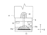
ヘッド5は、図2に示すように、金属製のツールからなる本体8の下部から順にセラミック製のセラミックホルダー9、セラミックヒータ10、およびセラミック圧子11で構成されている。なお、セラミックホルダー9はボルト12でツール本体8に装着されていると共に、セラミックヒータ10およびセラミック圧子11は、セラミックホルダー9に焼結されている。
【0042】
また、セラミック圧子11には温度検出手段13として、例えば、熱電対、測温抵抗体などが設けられている。つまり、セラミック圧子11がセラミックヒータ10から受ける熱を温度検出手段13で検出し、その検出結果を温度制御部21に送信する。
【0043】
セラミックホルダー9は、図3に示すように、セラミックヒータ10の発熱部分の上端面にエアーが流通して排出される第1流路15がセラミックホルダー9の下端部の長手方向(図3ではX方向)に貫通している。また、この第1流路15には、ツール本体8からエアーを供給するエアー供給流路16と連通接続されている。なお、このエアー供給流路16の他端には、図2に示すように、連通接続されたバルブVを備えた耐圧ホース17を介してエアー供給手段18からエアーが供給される。
【0044】
つまり、エアー供給手段18から供給されたエアーは、エアー供給流路16、エアー流路15の順を経て第1流路15両端の開口部15aから排出される。したがって、セラミックヒータ10の発熱部10aから発せられる熱がエアー循環により奪われ、セラミックヒータ10およびセラミック圧子11の両方を急速に冷却することができる。
【0045】
セラミックヒータ10は、図4に示すように、発熱部10aと端子部10bとをT字状に配した所定厚さ(例えば、1mm程度)のパネル体に形成されている。なお、セラミックヒータ10は、電気絶縁体材であるセラミック材で発熱体19を被覆した構成であり、かつ端子部10bから発熱体19の端子20を突出させている。
【0046】
なお、セラミックホルダー9、セラミックヒータ10のセラミック材およびセラミック圧子11は、窒化ケイ素に所定量のガラスなどが添加された材で構成されている。また、セラミックホルダー9の線膨張係数は、セラミックヒータ10およびセラミック圧子11の線膨張係数と同等であることが好ましい。さらに、それらの熱伝導率は、セラミックヒータ10を基点としてセラミック圧子11の加圧面側(図2では下方)へ向かう程大きいと共に、それと反対側(図2では上方)のセラミックホルター9の取付面側へ向かうほど小さいくなるようにすることが好ましい。
【0047】
温度制御部21は、使用する樹脂ごと応じた設定条件、例えば加熱時間、セラミックヒータ10の冷却温度としてのガラス転移点などが予め図示しない外部入力装置から入力されている。これら入力条件と温度検出手段から検出される検出結果とに基づいて、セラミックヒータ10の温度制御を行なっている。例えば、予め設定入力されたガラス転移点と温度検出手段13から送られる実測値とを比較し、求まる温度偏差に応じてセラミックヒータ10の温度を制御する。具体的には、バルブVを開きエアーを供給して温度がTg以下になるとバルブVを閉じ、ヘッドを上昇させる。
【0048】
次に上述の実施例装置を用いてチップを基板に実装する一巡の動作を図5のフローチャートに沿って説明する。なお、本実施例では、樹脂の硬化温度を220℃、ガラス転移点(Tg)を120℃に予め設定したものとする。また、本実施例では、前工程の仮圧着工程でチップが基板に予め仮圧着された状態で搬送されたものに対し、基板にチップを完全に本圧着する場合を例に採って説明する。
【0049】
<ステップS1> 基板の位置合わせ
前段の仮圧着工程で樹脂を介してチップ4が仮圧着された基板2が、図示しない搬送機構により、本圧着装置1へと搬送される。この基板4は、可動テーブル3の基板保持ステージ7に移載されて吸着保持される。基板保持ステージ7は図示しない駆動機構によって、前方(図1のY方向)である、ヘッド5とガラスバックアップ6との間に向かって移動し、ヘッド5とガラスバックアップ6とでチップ4を上下方向から挟み込めるように基板4の位置合わせを行なう。
【0050】
<ステップS2> チップの加熱圧着開始
基板2の位置合わせが終了すると、図示しない駆動機構によりヘッド5が下降し、このヘッド5と基板2の下側にあるガラスバックアップ6とでチップ4が挟み込まれる。ヘッド5は、基板2へのチップ4の加熱圧着を開始する。このとき、ヘッド5に備わったセラミックヒータ10は、図6に示すように、チップ4の加熱圧着の開始時点(t0)において温度制御部21により、220℃に設定されている。加熱圧着開始と同時に開始時点(t0)から加熱終了時点(t1)の所定時間、温度制御部21によりセラミックヒータ10の温度を220℃に保ちながらチップ4を基板2に加熱圧着する、結果、チップ4からの熱伝達により樹脂が加熱硬化し始める。
【0051】
<ステップS3> 冷却開始
加熱終了時点(t1)に到達すると、メイン制御部Mから加熱OFF信号が温度制御部21に送られ、この信号に基づいて温度制御部21からの命令信号がバルブVに送信されてバルブVが開放される。バルブVの開放によりエアー供給手段18からエアーの供給が開始される。エアーは耐圧ホース17、エアー供給流路16を経て第1流路15へと流れ込む。この流れ込んだエアーが第1流路15の両端開口部15aに向かって流通して排出される、結果、第1流路15の下方に配されたセラミックヒータ10およびセラミック圧子11を急速に冷却する。
【0052】
<ステップS4> ガラス転移点に達したか
冷却が開始されると同時に、セラミック圧子11に設けられた温度検出手段13により逐次にヘッド5の温度が検出され、その実測値が温度制御部21へと送られる。温度制御部21では、セラミックヒータ10の冷却温度として予め設定入力されたのガラス転移点(Tg)と実測値との比較処理が逐次実行される。ここで、検出結果がガラス転移点(Tg)に到達していなければ、このTgと実測値との比較処理を繰り返し行ないながら冷却を継続する。逆に、実測値がTgに到達(図6に示す時点t2)するとステップS5へと進む。
【0053】
つまり、セラミックヒータ10の温度をTgまで冷却することにより、ヘッド5によって加熱されているチップ4も冷却され、ひいてはチップ4を基板2に固着させる樹脂をも冷却する。特にこの冷却に伴って樹脂温度がガラス転移点(Tg)まで冷却されることで、樹脂が略完全に硬化する。
【0054】
なお、本実施例ではセラミックヒータ10の冷却温度を樹脂のガラス転移点(Tg)に設定しているが、この冷却温度は、使用する樹脂の種類に応じたガラス転移点(Tg)のプラス20℃以下の範囲内に設定することもできる。
【0055】
<ステップS5> 加圧解除
冷却温度がTgに到達すると、チップ4への加圧を解除し、ヘッド5を上方待機位置に復帰させる。このとき、温度制御部21からの命令信号によりバルブVが閉塞されると共に、次のチップ4を基板2に固着するために、セラミックヒータ10の温度を220℃(図6に示す時点t3)まで上昇するように温度制御を行なう。
【0056】
すなわち、樹脂がTgまで冷却されて略完全に硬化した状態でチップ4上方からの加圧が解除されるので、樹脂内のエアーの膨張が防止される。つまり、樹脂硬化によりエアーの膨張を抑え込むことができ、バンプ周りなどのボイドの発生を防止することができる。
【0057】
また、ヘッド5の加圧により弾性変形して接触面積が拡張された状態でバンプと基板電極との間に介在している導電粒子の弾性復帰を、樹脂硬化により抑え込むことができる。つまり、樹脂が硬化することにより、導電粒子の弾性変形の復元時における弾性応力に対して樹脂粘度が上回り導電粒子の弾性変形状態を維持できる。結果、バンプと導電粒子との間に発生していたボイドを解消することができる。
【0058】
<ステップS6> 基板の取り出し
ヘッド5の加圧が解除されると、基板保持ステージ7が基板受け渡し位置まで移動する。受け渡し位置に移動した基板2は、図示しない基板搬送機構によって基板収納ユニットに搬送されて基板回収マガジンに収納される。
【0059】
以上で1枚の基板2についてチップ4のボンディングが終了する。
【0060】
上述のように、チップ4を基板2に加熱圧着しながら樹脂を加熱硬化した後に、セラミックヒータ10を使用する樹脂ごとのガラス転移点(Tg)までエアーにより急速に冷却することでヘッド全体がTgまで冷却され、ひいては基板2にチップ4を固着する樹脂をもTgまで冷却することができる。しがたって、樹脂が略完全に硬化した状態となるので、この状態でチップ上方からの加圧を解除することにより、本発明者により確認された従来からの問題の発生原因を解消することができた。
【0061】
具体的には、従来法では樹脂が硬化する前の軟化状態でヘッド5を上昇させて加圧解除したとき、樹脂内に在るエアーの急激な膨張によりバンプ周りを覆うようにボイドが発生していた。しかし、本実施例では樹脂が硬化した状態で加圧を解除することで、樹脂粘度がエアーの膨張による応力を上回りボイドの発生を防止することができる。
【0062】
また、従来ACFやACPを使用したとき、導電粒子の弾性変形の復元によりチップが上方に持ち上げられ、バンプと導電粒子との間に空間が発生していた。しかし、本実施例では樹脂が硬化した状態でチップ上方からの加圧が解除されるので、樹脂粘度が導電粒子の弾性変形の復元により作用する弾性応力を上回り、バンプと基板電極との接続不良を防止することができる。
【0063】
<第2実施例>
上述の第1実施例では、チップ4を基板2に加熱圧着して略完全に固着させる本圧着装置について説明したが、本実施例では、基板2にチップ4を実装して仮圧着および本圧着可能なボンディング装置について説明する。なお、ボンディング装置としては、ヘッド周りの構成のみが第1実施例装置と異なるので、同一箇所については同一符号を付すに留め、異なる部分について説明する。
【0064】
図7は本発明に係るボンディング装置の概略構成を示した斜視図、図8はヘッド周りの要部構成を示した正面図である。
【0065】
図8に示すように、ボンディング装置100は、チップ4を吸着保持して基板上の樹脂Gが塗布された所定箇所に位置決め実装するとともに、基板2にチップ4を加熱圧着する実装・加熱圧着機構101と、基板2を水平保持する可動テーブル3と、基板2上の樹脂部にチップ4を圧着する際に基板2を下方から支持するガラスバックアップ6と、ガラスバックアップ6を加熱するヒータ102と、上方および下方のそれぞれから基板2に向けてエアーを供給するノズル103,104と、これら各構成を総括的に制御する制御部106とから構成されている。
【0066】
実装・加熱圧着機構101は、図7に示すようにその下部にチップ4を吸着保持するヘッド107を備え、上下(X)方向および水平(Z)方向に移動可能に構成されている。また、ヘッド内部には、図示しない、セラミックヒータを備えるとともに、このヒータを冷却するための冷却手段も備えている。なお、このヘッドの構成は第1実施装置と略同一構成であるので詳しい説明を省略する。また、ヘッド107の構成としては、この形態に限定されるものではなく、例えば、ヘッド内に冷却手段を備えない構成であってもよい。
【0067】
可動テーブル3は、基板2を吸着保持する基板保持ステージ7を備え、この基板保持ステージ7が水平2軸(X,Y)方向、上下(Z)方向、およびZ軸周り(θ)方向に、それぞれ移動自在に構成されている。
【0068】
ヒータ102はガラスバックアップ6を加熱し、その熱を基板2および基板上の樹脂Gに伝達させて加熱するためのものである。このヒータ102は、図8に示すように、基板2から所定距離をおいたガラスバックアップ6の側壁に取り付けられており、制御部106の制御信号を受けた電圧コントローラ108により温度制御されている。
【0069】
基板下方に配備したノズル103は、ガラスバックアップ6を加熱したときにガラスバックアップ6が基板2に接触する部分の近傍領域の熱伝達を抑制するためのものであって、基板裏面に向けてエアーを供給するようになっている。
【0070】
また、基板上方に配備したノズル104は、加熱圧着後のチップ4を冷却するためのものであって、チップ実装部分に向けてエアーを供給するようになっている。
【0071】
なお、両ノズル103,104は、制御部106からの制御信号に応じてバルブVの開閉操作によりエアー供給源109からエアーが供給されるようになっている。
【0072】
制御部106は、実装・加熱圧着機構101がチップ4を基板2に実装するときの接地速度の調節、ガラスバックアップ6を加熱するヒータ102の温度調節、および基板2およびチップ4を冷却するためのノズル103,104からのエアー供給の調節などを総括的に行っている。なお、具体的な各部の制御については後述する。
【0073】
次に、上述のボンディング装置を用いて基板上に塗布した樹脂(ACF)部分にチップを実施する場合であって、基板へのチップ実装前に樹脂温度を調節しながら基板にチップを実装し、その後に仮圧着工程、本圧着工程および冷却工程を経て基板にチップを固着する方法につてい説明する。以下、具体的な方法について、図9のフローチャートおよび図10の温度プロファイルに沿って説明する。なお、図10に示す温度プロファイルは、説明の便宜上、チップ実装後からを示している。
【0074】
<ステップS10> 基板の位置合わせ
基板2が、図示しない搬送機構により、ボンディング装置100へと搬送される。この基板4は、可動テーブル3の基板保持ステージ7に移載されて吸着保持される。基板保持ステージ7は図示しない駆動機構によって、前方(図7のY方向)である、ヘッド107とガラスバックアップ6との間に向かって移動し、ヘッド107とガラスバックアップ6とでチップ4を上下方向から挟み込めるように基板2の位置合わせを行なう。
【0075】
<ステップS11> 樹脂の加熱
位置合わせ終了後、ヒータ102が作動してガラスバックアップ6を加熱し、その熱が基板上の樹脂Gに伝達されて樹脂Gを軟化させる。本実施例の場合、樹脂がACFであるので樹脂温度が60〜120℃の範囲内に設定される。好ましくは、80〜100℃である。樹脂温度が60℃を下回ると樹脂Gが十分に軟化しないのでチップ4を実装した際にチップ4と樹脂Gの界面などに巻き込むエアーが逃げずらくなる、結果、界面などに残ったエアーがボイドとなる。また、樹脂温度が120℃を超えると、樹脂Gが硬化してしまう。
【0076】
<ステップS12> チップの実装
所定箇所にあるチップ4をヘッド107により吸着保持して基板上の軟化状態にある樹脂部に位置決め実装する。この樹脂上にチップ4を実装するとき、その接地速度が10mm/s以下に設定される。好ましい範囲は1〜5mm/sである。接地速度が10mm/sを超えると、樹脂部へのチップ4の押圧時にエアーの逃げる合間がなくなってしまう。
【0077】
チップ4が実装されるとヒータ102による加熱を停止する。
【0078】
<ステップ13> 第1加熱工程
仮圧着工程に相当する第1加熱工程では、使用する樹脂Gに応じて加熱した際に樹脂Gからガス(以下、単に「アウトガス」という)の発生しない設定温度で所定時間、ヘッド107でチップ4を押圧しながら樹脂Gを所定の粘度以上となるように加熱硬化させる。ここでいう所定粘度とは、次の第2加熱過程で樹脂Gを高温加熱した際に発生するアウトガスの発生応力を抑えることのできる粘度をいう。
【0079】
なお、第1加熱工程における設定温度は、例えば樹脂GがACFの場合、図10に示すように、t0〜t1の第1加熱工程の間、樹脂温度が190℃未満(図10では170℃)となるようにヘッド内のヒータ温度を調節している。この設定温度は、好ましくは、120〜170℃である。
【0080】
設定温度が120℃を下回ると樹脂Gの硬化速度が遅くなるとともに、十分な樹脂粘度を得ることができない。逆に設定温度が190℃を超えるとアウトガスを発生させる。つまり、未硬化の状態にある樹脂粘度よりもアウトガスの発生応力が上回り、チップ4と基板2の界面などにボイド等を発生させることになる。
【0081】
また、図10に示すt0〜t1の加熱時間としては、20秒以内に設定される。好ましくは、1〜5秒である。通常ACFの場合、設定温度が180〜190℃において、20秒で硬化する必要があるが、それ以下の時間でもボイド無く硬化することができる。
【0082】
なお、設定温度と加熱時間については、使用する樹脂の硬化条件などに応じて適宜に設定変更される。
【0083】
<ステップ14> 第2加熱工程
第1加熱工程での樹脂の加熱硬化が終了すると連続して、図10に示すt1〜t2の間、先の第1加熱工程での加熱温度よりも高い温度で樹脂を加熱硬化する。このときの設定温度は、樹脂が190℃以上となるようにヘッド内のヒータ温度を調節している。この設定温度として好ましくは、200〜220℃の範囲である。第2加熱温度が190℃を下回ると樹脂の硬化促進を損なうからである。
【0084】
すなわち、第2加熱工程では、先の第1加熱工程で樹脂粘度を予め高めているので、190℃以上に温度を上げて樹脂がアウトガスを発生しても、樹脂粘度がアウトガス発生応力を抑えることができる、結果、ボイドなどの発生を防止することができる。また設定温度が220℃を超え、さらに240℃以上になると、樹脂の耐熱上の問題がある。
【0085】
なお、樹脂Gを加熱する第2加熱工程の設定時間としては、本実施例の場合、例えば2秒に設定されている。
【0086】
ここで、第1加熱工程開始(t0)から第2加熱工程終了(t2)までの時間を20秒以内に設定することもできる。この場合においても、ボイドを発生させることなく樹脂Gを硬化させることができる。
【0087】
なお、この第2加圧工程は、本圧着工程に相当する。
【0088】
<ステップ15> 冷却開始
第2加熱工程が終了すると、図10のt2の時点から樹脂温度がガラス転移点(t3の時点)となるように冷却が開始される。具体的には、以下の手順で冷却が行なわれる。
【0089】
先ず、第1実施例の本圧着装置と同様に、制御部106から加熱OFF信号に基づいて図示しないバルブVが開放されヘッド内にエアーの供給が開始される。このエアーの供給に伴ってヘッド内のセラミックヒータおよびセラミック圧子を急速に冷却する。このとき、樹脂Gは大気開放状態による冷却とヘッド107を積極的に冷却することによる伝熱で冷却効果を受ける。
【0090】
所定の条件の温度に到達するとヘッド107の冷却を停止し、制御部106はバルブVを開放操作して基板上方のノズル104からチップ4に向けてエアーを供給するとともに、ヒータ102の温度により調節をする。すなわち、樹脂Gの温度がガラス転移点近傍であって、かつ基板2とチップ4が大気開放の室温状態からの熱膨張量が略等しくなるようにチップ4と基板2の温度調節を行う。したがって、チップ4と基板2が冷却により収縮するときに発生しがちな反りを防止することができる。
【0091】
なお、これら温度調節の時間や条件の設定方法としては、事前テストにより、チップ4、基板2、および樹脂Gの各温度を測定しながら条件設定を行う。
【0092】
また、本実施例における基板2の熱膨張量とは、基板全体の熱膨張量を意味するのではなく、チップ4が実装された部分とその部分を取り囲む所定領域内の基板2の熱膨張量をいう。この領域は、チップ4のサイズなどによって任意に設定される。
【0093】
<ステップ16> 加圧解除
冷却温度がガラス転移点に到達すると、ヘッド107によるチップ4への加圧を解除し、ヘッド107を上方待機位置に復帰させる。
【0094】
<ステップ17> 基板取り出し
ヘッド107の加圧が解除されると、基板保持ステージ7が基板受け渡し位置まで移動する。受け渡し位置に移動した基板2は、図示しない基板搬送機構によって基板収納ユニットに搬送されて基板回収マガジンに収納される。
【0095】
以上で1枚の基板2についてチップ4のボンディングが終了する。
【0096】
次に、本発明者は、第2実施例装置を用いてチップを基板に実装するときの接地速度(ヘッドスピード)とチップ実装時の樹脂軟化温度を変更したときのボイドの発生状況を確認する実験を行った。その結果を以下に説明する。
【0097】
<具体例>
ガラス基板として高透明度クラウンガラスを使用し、この基板上の電極部分に塗布する樹脂としてACFを使用する。このときのACFに含まれる粒子径が3.5μmであって単位面積当たりの粒子数が100万個/mm3のものを厚さ35μmとなるようにガラス基板に塗布した。
【0098】
また、ACFの推奨接合条件、つまり、この使用する樹脂が加熱によりアウトガスを発生しない温度として190℃未満、樹脂を略完全硬化する温度を220℃にした。
【0099】
また、基板にチップを実装するときのヘッドスピードを1、3、5、10(mm/s)の4パターンとし、各接地速度で基板にチップを実装するときの樹脂温度を150、170、180、200、220(℃)のそれぞれについて実験を行った。なお、各樹脂温度は、終始一定のまま樹脂が硬化するまで加熱した。以下、実験により得られた結果を表1に示す。
【0100】
なお、各条件でのポイント数は次のようにして求めている。バンプ周りおよびバンプ周り以外の領域に発生しているボイドと、ボイドよりも大形である亀裂の発生のそれぞれを基板の裏面側から目視により確認し、その個数に応じてポイント数を求めている。具体的には、ボイドについては所定領域ごと確認できない場合、領域ごとに「0」ポイントを付与し、数個確認できた場合、領域ごとに「1」ポイント、数十個確認できた場合、「2」ポイントを付与している。また、亀裂についても同じ配点とし、ボイドと亀裂のそれぞれのポイントを加算して求めている。
【0101】
【表1】
【0102】
表1からも明らかなように樹脂温度170℃のときにヘッドスピードを5mm/sでチップを基板に実装して樹脂を硬化したときにポイント数は「0」であって、ボイドなどを一切確認することのない良好なチップ実装を実現できることが確認できた。すなわち、チップ実装時にチップと樹脂との界面などに巻き込んだエアーの全てが排出されたことを意味する。また、推奨接合条件の190℃以下でヘッドスピードを1〜10mm/sの範囲に設定することにより、エアーの巻き込みによるボイドなどの発生を低減できることも確認できた。
【0103】
なお、樹脂の軟化温度が150℃と200℃以上のときにボイドなどの発生ポイントが高い理由は次の通りである。
樹脂軟化温度が150℃であるとACF推奨接合条件よりも低すぎて樹脂自体が十分に軟化していないので、チップと樹脂との界面に巻き込んだエアーが逃げ切れずに包含されてしまうためである。
【0104】
また、樹脂軟化温度が200℃以上の場合、ACFの推奨接合条件であるアウトガスが発生しない温度を超えているためであって、アウトガスの発生が起因したボイドなどである。
【0105】
以上のように、基板上のチップ実装箇所の樹脂Gを予め加熱して軟化させておくとともに、樹脂Gにチップ4が接地するときの接地速度を制御することにより、実装時にチップ4と樹脂Gの界面などに巻き込むエアーが排出除去され、結果、エアーの巻き込みによる樹脂硬化後のボイドなどの発生を防止することができる。
【0106】
また、チップ実装後の第1加熱工程において、使用する樹脂Gに応じて加熱したときにアウトガスの発生しない温度で所定時間、樹脂Gを予め加熱硬化し、その後の第1加熱工程の温度よりも高い温度により樹脂Gを略完全に硬化させる第2加熱工程を経ることにより、第1加熱工程の時点で樹脂粘度が第2加熱過程で発生するアウトガスの発生応力を上回るので、アウトガスの発生が起因するボイドや亀裂などを防止することができる。
【0107】
また、第2加熱工程後に樹脂Gをガラス転移点に冷却するとき、樹脂Gの温度がガラス転移点近傍であって、かつ基板2とチップ4の室温からの熱膨張量が等しくなるようにチップ4にエアーを供給して冷却するとともに、ガラス転移点よりも低い温度になる基板2をヒータ102で加熱しながら、両部材の温度を調節することにより、熱膨張量を制御しないで両部材を冷却したときに発生していた反りを解消することができる。
【0108】
さらに、ガラス転移点に到達して樹脂Gが略完全に硬化した状態でヘッド107の加圧を解除するので、基板2とチップ4の熱膨張量の差によって発生しがちな反りを一層確実に解消することができる。
【0109】
本発明は、上記の実施例に限らず、次のように変形実施することもできる。
【0110】
(1)第1実施例では、前段の仮圧着工程で基板の所定箇所にチップを予め仮圧着した基板に対し、チップを基板に完全に固着する本圧着を行なっていたが、仮圧着することなく本圧着のみの一括工程でチップを基板に実装するようにしてもよい。
【0111】
この場合、ヘッド5の下端部にチップ4を吸着保持するための吸着孔を設けると共に、基板2の下方側に認識手段を設けて、基板保持ステージ7に載置された基板2上のマーク位置とチップ4のマーク位置を認識させて位置合わせを行なうようにすればよい。
【0112】
(2)第1実施例では、ヘッド5にセラミックヒータ10を備え、チップ4の上方からのみ樹脂を加熱していたが、基板保持ステージ7側のみ、若しくはチップ4の上方および基板保持ステージ側の両方にセラミックヒータなどの加熱手段を設けてもよい。この場合、基板保持ステージ7側のヒータ温度を、使用する樹脂のガラス転移点(Tg)と同じに設定することが好ましい。
【0113】
このように、基板保持ステージ7側の加熱手段をTgに設定しておくことにより、樹脂が略完全に硬化するときのチップ4と基板2の温度を同じにすることができる。したがって、従来のヘッド5側からのみ加熱して樹脂を加熱硬化していたときにチップ4側と基板2側の線膨張係数の差により発生しがちであった基板2の反りによる歪みを解消することができる。
【0114】
また、加熱手段としては、セラミックヒータに限定されるものではなく、樹脂を加熱硬化できる手段であればよい。
【0115】
(3)第1実施例では、冷却手段としてセラミックヒータ10の上面側に沿うように第1流路15を設けていたが、以下のように変形実施しいてもよい。
【0116】
<変形例1>
ヘッド5の斜視図である図11およびその側面図である図12に示すように、セラミックホルダー9の側壁に水平方向に貫通する貫通孔22を設け、この貫通孔内部に外部から送風手段などでエアーを吹き付けてエアーを流通させるようにしてもよい。
【0117】
なお、この貫通孔22は、図11に示すように、ヘッド5の内部にエアーを供給する上記実施例のヘッド5の構成に組み合わせてもよいし、貫通孔22のみによるヘッド5の冷却を実施するようにしてもよい。
【0118】
<変形例2>
ヘッド5の正面図である図13に示すように、セラミックホルダー9およびツール本体8の側壁の基端側から水平方向に延びるテーパー状の放熱用冷却部材23(フィン)を多段に取り付けてもよい。このように、複数のフィン23を取り付けることによりヘッド5の放熱効果の向上を図ることができ、ひいてはヘッド5の冷却を行なうことができる。
【0119】
なお、フィン23は、放熱効果の高い部材が好ましく、例えば金属であることが好ましい。
【0120】
また、このフィン23は、図12に示すように、ヘッド5の内部にエアーを供給する第1実施例のヘッド5の構成に組み合わせてもよいし、フィン23のみによるヘッド5の冷却を実施するようにしてもよい。
【0121】
<変形例3>
第1実施例および各変形例ではエアーにより冷却を実施しいていたが、冷却水を利用してセラミックヒータ10を冷却するようにしてもよい。具体的には、図14の側面図に示すように、冷却水供給手段24から供給した冷却水をセラミックヒータ10の上方に沿って循環するように「U」字状の第2流路25を設けてもよい。
【0122】
(4)第1実施例では、ヘッド5の冷却にエアーや冷却水を利用していたが、他の冷却媒体を利用してもよい。例えば、液体窒素を第2流路に供給循環させるなどしてもよい。
【0123】
(5)第2実施例では、1台のボンディング装置100を用いて仮圧着工程と本圧着工程のそれぞれ実施していたが、仮圧着工程と、本圧着工程の装置を別に設けるようにしてもよい。この場合、本圧着装置は、仮圧着工程で基板上に仮圧着されたチップ4を加熱圧着するのみなので、ヘッド部分にチップ4を吸着保持する機能を有さなくてもよい。
【0124】
このように仮圧着装置と本圧着装置とを個別にすることにより、量産性を向上できる。
【0125】
(6)第2実施例では、チップ実装前に樹脂を軟化させる手段としてガラスバックアップ6を介してヒータ102の熱を樹脂Gに伝達させていたが、例えば基板上方にノズル等を配備し、熱風を樹脂に向けて供給して軟化させるようにしてもよい。また、基板上方を移動可能なヒータを備えたアームを樹脂近傍に移動させ、ヒータの輻射熱を利用して非接触状態で樹脂を軟化させてもよい。
【0126】
【発明の効果】
以上の説明から明らかなように、本発明によれば、樹脂を介してチップを基板に加熱圧着した後に、その樹脂のガラス転移点まで加熱圧着手段を冷却して加熱圧着手段によるチップの加圧を解除する。したがって、加熱圧着手段の冷却に伴って樹脂自体がガラス転移点まで冷却されて略完全に硬化するので、樹脂内部に含まれるエアーの膨張を抑制できる、結果、エアーの膨張によるボイドの発生を防止することができる。また、導電粒子の圧接のゆるみの発生を抑え、接続抵抗値を低く保つことができる。
【図面の簡単な説明】
【図1】 第1実施例に係る本圧着装置の概略構成を示した斜視図である。
【図2】 第1実施例装置に係るヘッドの要部構成を示した正面図である。
【図3】 第1実施例装置に係るヘッドの要部構成を示した側面図である。
【図4】 セラミックヒータの要部構成を示した斜視図である。
【図5】 ボンディング方法を示したフローチャートである。
【図6】 ヘッドの温度制御プロファイルを示した図である。
【図7】 第2実施例装置に係るボンディング装置の概略構成を示した斜視図である。
【図8】 第2実施例装置に係るヘッド周りの要部構成を示した正面図である。
【図9】 第2実施例装置を用いたボンディング方法を示したフローチャートである。
【図10】 ヘッドの温度制御プロファイルを示した図である。
【図11】 第1変形例のヘッドの要部構成を示した斜視図である。
【図12】 第1変形例のヘッドの要部構成を示した側面図である。
【図13】 第2変形例のヘッドの要部構成を示した正面図である。
【図14】 第3変形例のヘッドの要部構成を示した側面図である。
【図15】 従来方法によりチップを基板にボンディングしたときの断面図である。
【図16】 従来方法によりチップを基板にボンディングしたときの断面図である。
【図17】 従来方法によりチップを基板にボンディングしたときの断面図である。
【図18】 図13のA−A矢視断面図である。
【図19】 従来方法によりチップを基板にボンディングしたときの断面図である。
【図20】 従来方法によりチップを基板にボンディングしたときの断面図であって(a)は平面からの断面図、(b)は(a)の矢印X方向から見たときの縦断面図である。
【符号の説明】
2 … 基板
3 … 可動テーブル
4 … チップ
5,107 … ヘッド
6 … ガラスバックアップ
10 … セラミックヒータ
15 … 第1流路
16 … エアー供給路
18 … エアー供給手段
21 … 温度制御部
102 … ヒータ
103,104 … ノズル
106 … 制御部[0001]
BACKGROUND OF THE INVENTION
The present invention relates to a bonding method and apparatus for mounting a mounting member such as a semiconductor element or a surface mounting component on a substrate such as a resin substrate or a glass substrate, and more particularly to a technique for mounting the mounting member on the substrate with high accuracy. .
[0002]
[Prior art]
Conventionally, in a manufacturing process of a substrate (for example, a flat display panel such as a liquid crystal, an EL (Electro Luminescence), or a plasma display), a mounting member (for example, a semiconductor chip) is mounted on the substrate. As a bonding method for mounting a mounting member (hereinafter simply referred to as “chip”) on a substrate, a resin such as an anisotropic conductive film (ACF) or a non-conductive resin (NCP) is used between the substrate and the chip. Non-Conductive Paste) and the like are interposed, and the thermocompression bonding means is pressed from above the chip, the resin is heat-cured and the chip is thermocompression bonded to the substrate.
[0003]
[Problems to be solved by the invention]
However, such a bonding method has the following problems. For example, when a chip is mounted on a substrate by heating and curing while pressing ACF, NCP, or the like, out-gas is generated from the resin when the resin is cured at a high temperature, as shown in the cross-sectional views of chip mounting in FIGS. In addition, a void 32 (shown in FIG. 15) covering the periphery of the
[0004]
Further, as shown in the cross-sectional view of the chip mounting in FIG. 17 and the cross-sectional view in the direction of arrows AA in FIG. 17 shown in FIG. 18, the resin once cured through the conductive particles is completely cured (below the glass transition point). Since the pressure is removed before the temperature is lowered), the resin is loosened and the
[0005]
Further, both the
[0006]
The present invention has been made in view of such circumstances, and a main object of the present invention is to provide a bonding method and apparatus for mounting a mounting member on a substrate with high accuracy.
[0007]
[Means for Solving the Problems]
It is common general knowledge in the industry that the cause of void generation during conventional chip mounting is outgas generated by resin or air entrapment. Therefore, in this industry, the following measures are taken in order to prevent the occurrence of this void.
[0008]
(1) Measures for preventing outgas generation suppress outgas generation by performing the resin curing temperature at a low temperature.
[0009]
(2) The measure to prevent air entrapment is to increase the viscosity of the resin and make it difficult for air to enter the resin.
[0010]
However, the present situation is that the occurrence of voids cannot be sufficiently prevented even if the above-described measures are taken.
[0011]
Therefore, in order to prevent the generation of voids, we developed an apparatus that can observe the cured state of the resin being bonded to the glass substrate with a microscope from the bottom, and as a result of multifaceted studies, the present inventors have found that the following phenomenon occurs. Could get. In the experiment, an NCP or ACF resin having a curing temperature of 220 ° C. and a glass transition point of 120 ° C. was used.
[0012]
The resin is still in a softened state at the stage where heat of 220 ° C. is constantly applied from the thermocompression bonding means and the chip is thermocompression bonded to the substrate. When the pressure applied by the pressurizing unit is released while the resin is not cured, the air that was in the state where the pressure was applied to the inside of the resin immediately expands (several times). Void 32 (shown in FIG. 15) covering the periphery of the bump and the
[0013]
In addition, when ACF or ACP is used, the conductive particles on the bump (the surface of the polymer plated with gold, nickel, etc.) bite into the bump while being elastically deformed by pressing from above the chip. The electrical connection is maintained. However, since the resin is still in a softened state immediately after releasing the pressurization by the pressurizing means, if the substrate is warped, the one that has been flattened by the pressurization will return to the original elasticity. The resin viscosity is lost to the stress, and a portion where a gap increases between the bump and the electrode is formed. As this gap increases, the elastic deformation of the conductive particles is restored as shown in FIGS.
[0014]
Specifically, a space is generated between the concave portion of the bump portion formed by the biting of the conductive particles and the
[0015]
That is, when the resin is heat-cured, the air contained in the resin is not expanded even if the pressure from the top of the chip is released, and in the case of ACF, the conductive particles when the pressure is released. In order to prevent the resin viscosity from losing the elastic stress due to the restoration, the pressure was released after the resin was cooled below the Tg temperature.
[0016]
In order to achieve such an object, the present invention has the following configuration.
That is, the invention according to
During the process of pressurizing the mounting member to the substrate by the pressurizing means, the mounting member or at least one side of the substrate is heated so that the resin is raised to a temperature at which the curing reaction starts and the temperature is maintained until the curing reaction is completed. A thermocompression bonding process of heating by means;
When the heating means is cooled in a state where the mounting member is pressurized, the substrate is mounted so that the temperature of the resin is near the glass transition point and the thermal expansion amount from room temperature of the substrate and the mounting member is substantially equal. A cooling process for adjusting the temperature of at least one of the members,
And when the said heating means is cooled and the said resin reaches the glass transition point vicinity, the mounting member is completely fixed to a board | substrate by releasing the pressurization of the mounting member by the said pressurization means. Is.
[0017]
(Operation / Effect) In the process of interposing a resin between a mounting member (for example, a chip) and the substrate and pressurizing the mounting member against the substrate by the pressing means, at least one side of the mounting member or the substrate is heated by the heating means. The resin is heated and cured while heating, and the mounting member is heated and pressure-bonded to the substrate. When the mounting member is thermocompression-bonded to the substrate, the heating means is cooled, and thereafter the pressurization by the pressurizing means from above the chip is released. That is, the resin itself is cooled with the cooling of the heating means. Accordingly, since the pressure from above the chip is released in a state where the resin is substantially cured, it is possible to suppress expansion due to the removal of the external pressure of the air contained in the resin in the pressurized state. it can. As a result, voids that have occurred around the bumps or straddled between the bumps due to the expansion of air can be prevented, thus preventing poor conduction between the bumps and the substrate electrode due to the occurrence of voids and shorting between the bumps. be able to.
[0018]
Further, during the cooling process, the resin temperature becomes close to the glass transition point, and at this time, at least one of the temperature of the substrate and the mounting member is adjusted so that the thermal expansion amounts of the substrate and the mounting member from room temperature become substantially equal. Therefore, it is possible to avoid the bonding failure and the resistance value failure that occur due to the mounting member and the substrate warping due to the difference in shrinkage between the substrate and the mounting member. In addition, the amount of thermal expansion of a board | substrate here means the amount of thermal expansion of the board | substrate part corresponding to the length of the chip | tip as a mounting member, for example.
[0019]
According to a second aspect of the present invention, in the bonding method according to the first aspect, the temperature of the substrate and the mounting member is adjusted by at least one of cooling the mounting member and heating the substrate. To do.
[0020]
(Operation / Effect) When the mounting member is directly heated from the mounting member side and mounted on the substrate, the temperature increases in the order of the distance from the heating means, that is, the mounting member, resin, and substrate. Further, since the substrate side is not heated, the substrate itself has a heat dissipation effect, and the temperature difference between the mounting member and the substrate becomes large. In this case, the mounting member side is actively cooled, or the substrate side is heated naturally or actively while the substrate side is open to the atmosphere, and the substrate temperature is heated so that the resin temperature is near the glass transition point. The temperature of both members is adjusted so as to eliminate the expansion difference. As a result, the method described in
[0021]
Further, the invention according to
[0022]
(Operation / Effect) A resin is interposed between the mounting member and the substrate, the pressure is applied by the pressurizing means, and the mounting member is thermocompression bonded to the substrate while being heated by the heating means. After the mounting member is thermocompression bonded to the substrate, the heating means is cooled to + 20 ° C. or lower of the glass transition point of the resin used. With this cooling, the resin itself is also cooled to reach a substantially cured state. As a result, the method according to
[0023]
Also,
A holding table for mounting and holding the substrate;
First pressurizing means for pressurizing the mounting member to a predetermined portion of the held substrate;
Heating means for heating and curing the resin by heating the mounting member in a pressurized state to a temperature at which the resin initiates a curing reaction;
Second heating means for heating the substrate placed on the holding table;
A cooling means for cooling the heating means in a pressurized state of the mounting member;
When the resin is cooled to the vicinity of the glass transition point, the temperature of the resin is in the vicinity of the glass transition point, and at least one of the substrate plate and the mounting member is such that the amount of thermal expansion from the room temperature of the substrate and the mounting member is substantially equal. Temperature control means for controlling the cooling means and the second heating means on the holding table side based on the temperature of the mounting member and the substrate so as to adjust the temperature of
It is characterized by comprising.
[0024]
(Operation / Effect) The mounting member is pressed by the pressing means through the resin mixed with the conductive particles at a predetermined position on the substrate placed and held on the holding table, and the substrate is heated by the heating means. Crimped to Then, after the heating means that heats the mounting member is cooled, the pressure on the mounting member is released. Therefore, as the heating means is cooled, the resin itself is also cooled and completely cured. As a result, the method according to
[0025]
In addition, the temperature of both members is adjusted so that the resin temperature becomes near the glass transition point during the cooling process, and at this time, the amount of thermal expansion from the room temperature of the substrate and the mounting member becomes substantially equal. Therefore, the method according to
[0026]
Also,
[0027]
(Operation / Effect) The temperature is controlled so that the cooling of the cooling means becomes + 20 ° C. or less of the glass transition point of each resin used. Therefore,
[0028]
Also,
[0029]
Also,
[0030]
Also,
[0031]
Also,
[0032]
Also, Claim 10 The invention described in Claim 14 In the bonding apparatus according to
It faces the heater member.
[0033]
(Operation / Effect) Air is blown by the air blowing means toward the through hole which is the air supply flow path provided in the heating means ( Claim 6 ), Supplying air to the first flow path provided inside the heating means ( Claim 7 ), Mounting a cooling member for heat dissipation on the outer periphery of the heating means ( Claim 8 ) Supply and circulate cooling water to the second flow path provided inside the heating means ( Claim 9 ) And a second flow path facing the heater pattern provided on the heater member ( Claim 10 )
[0034]
Also, Claim 11 The invention described in
[0035]
(Operation / Effect) The substrate placed and held on the holding table is heated by the heating means provided on the holding table side. In other words, since the holding table is set so that the glass transition point of each resin used for mounting the mounting member is not more than 20 ° C., there is no temperature difference between the mounting member and the substrate at the time of cooling. It is possible to prevent the warpage of the substrate caused by the difference in the coefficient of linear expansion of the members.
[0036]
DETAILED DESCRIPTION OF THE INVENTION
<First embodiment>
In this embodiment, a case where a chip as a mounting member is mounted on a substrate using a resin such as ACP, ACF, NCP, or NCF will be described as an example.
The “mounting member” in the present invention includes, for example, types and sizes of IC chips, semiconductor chips, optical elements, surface mount components, chips, wafers, TCP (Tape Carrier Package), FPC (Flexible Printed Circuit), and the like. Regardless of the above, all forms on the side to be bonded to the substrate are shown, and COG (Chip On Glass), which is chip bonding to a flat display panel, TCP, and OLB (Outer Lead Bonding), which is FPC bonding, can be considered.
[0037]
In addition, the “substrate” in the present invention refers to all forms on the side to be bonded to the mounting member, regardless of the type of resin substrate, glass substrate, film substrate, chip, wafer, and the like.
[0038]
First, the apparatus used in the present embodiment will be specifically described with reference to the drawings.
FIG. 1 is a perspective view showing a schematic configuration of the present crimping apparatus which is a bonding apparatus according to the present invention, FIG. 2 is a front view showing the configuration of the main part of the head portion of the embodiment apparatus, and FIG. 3 is a head of the embodiment apparatus. It is the side view which showed the principal part structure of the part.
[0039]
As shown in FIG. 1, the
[0040]
As shown in FIG. 1, the movable table 3 includes a
[0041]
As shown in FIG. 2, the
[0042]
Further, the
[0043]
As shown in FIG. 3, the
[0044]
That is, the air supplied from the air supply means 18 is discharged from the
[0045]
As shown in FIG. 4, the
[0046]
The
[0047]
The
[0048]
Next, a round operation of mounting the chip on the substrate using the above-described embodiment apparatus will be described with reference to the flowchart of FIG. In this example, it is assumed that the curing temperature of the resin is preset to 220 ° C. and the glass transition point (Tg) is set to 120 ° C. Further, in this embodiment, a case where the chip is completely press-bonded to the substrate will be described as an example in contrast to the case where the chip is transported in a pre-press-bonded state to the substrate in the preliminary press-bonding process of the previous process.
[0049]
<Step S1> Substrate alignment
The
[0050]
<Step S2> Start of chip thermocompression bonding
When the alignment of the
[0051]
<Step S3> Cooling start
When the heating end point (t1) is reached, a heating OFF signal is sent from the main control unit M to the
[0052]
<Step S4> Has the glass transition point been reached?
Simultaneously with the start of cooling, the temperature of the
[0053]
That is, by cooling the temperature of the
[0054]
In this embodiment, the cooling temperature of the
[0055]
<Step S5> Pressure release
When the cooling temperature reaches Tg, the pressure on the
[0056]
That is, since the pressure from the upper side of the
[0057]
Further, the elastic recovery of the conductive particles interposed between the bump and the substrate electrode in a state where the contact area is expanded by being elastically deformed by pressurization of the
[0058]
<Step S6> Removing the substrate
When the pressurization of the
[0059]
Thus, the bonding of the
[0060]
As described above, after the resin is heated and cured while thermocompression bonding the
[0061]
Specifically, in the conventional method, when the
[0062]
Further, when an ACF or ACP is conventionally used, the chip is lifted upward by restoring elastic deformation of the conductive particles, and a space is generated between the bump and the conductive particles. However, in this embodiment, the pressure from the top of the chip is released while the resin is cured, so the resin viscosity exceeds the elastic stress acting by restoring the elastic deformation of the conductive particles, and the connection between the bump and the substrate electrode is poor. Can be prevented.
[0063]
<Second embodiment>
In the first embodiment described above, the main pressure bonding apparatus has been described in which the
[0064]
FIG. 7 is a perspective view showing a schematic configuration of the bonding apparatus according to the present invention, and FIG. 8 is a front view showing a main configuration around the head.
[0065]
As shown in FIG. 8, the
[0066]
As shown in FIG. 7, the mounting /
[0067]
The movable table 3 includes a
[0068]
The
[0069]
The
[0070]
The
[0071]
Both
[0072]
The
[0073]
Next, in the case where the chip is applied to the resin (ACF) portion applied on the substrate using the bonding apparatus described above, the chip is mounted on the substrate while adjusting the resin temperature before mounting the chip on the substrate, After that, a method for fixing the chip to the substrate through the provisional pressure bonding process, the main pressure bonding process, and the cooling process will be described. Hereinafter, a specific method will be described along the flowchart of FIG. 9 and the temperature profile of FIG. Note that the temperature profile shown in FIG. 10 is shown after chip mounting for convenience of explanation.
[0074]
<Step S10> Substrate alignment
The
[0075]
<Step S11> Heating of resin
After the alignment is completed, the
[0076]
<Step S12> Chip mounting
The
[0077]
When the
[0078]
<Step 13> First heating step
In the first heating process corresponding to the pre-bonding process, the
[0079]
The set temperature in the first heating step is, for example, when the resin G is ACF, as shown in FIG. 10, the resin temperature is less than 190 ° C. during the first heating step from t0 to t1 (170 ° C. in FIG. 10). The heater temperature in the head is adjusted so that This set temperature is preferably 120 to 170 ° C.
[0080]
When the set temperature is lower than 120 ° C., the curing rate of the resin G becomes slow and a sufficient resin viscosity cannot be obtained. Conversely, when the set temperature exceeds 190 ° C., outgas is generated. In other words, the outgassing stress exceeds the uncured resin viscosity, and voids are generated at the interface between the
[0081]
Also, the heating time from t0 to t1 shown in FIG. 10 is set within 20 seconds. Preferably, it is 1 to 5 seconds. Usually, in the case of ACF, it is necessary to cure in 20 seconds at a set temperature of 180 to 190 ° C., but it can be cured without voids even at a time shorter than that.
[0082]
In addition, about setting temperature and heating time, a setting change is suitably carried out according to the hardening conditions etc. of resin to be used.
[0083]
<Step 14> Second heating step
When the heat curing of the resin in the first heating step is completed, the resin is heat cured at a temperature higher than the heating temperature in the previous first heating step during t1 to t2 shown in FIG. At this time, the heater temperature in the head is adjusted so that the temperature of the resin is 190 ° C. or higher. This set temperature is preferably in the range of 200 to 220 ° C. This is because when the second heating temperature is lower than 190 ° C., acceleration of curing of the resin is impaired.
[0084]
That is, in the second heating step, since the resin viscosity is increased in advance in the first heating step, even if the temperature is raised to 190 ° C. or higher and the resin generates outgas, the resin viscosity suppresses the outgas generation stress. As a result, generation of voids can be prevented. When the set temperature exceeds 220 ° C. and further exceeds 240 ° C., there is a problem in heat resistance of the resin.
[0085]
In the present embodiment, the set time of the second heating process for heating the resin G is set to 2 seconds, for example.
[0086]
Here, the time from the start of the first heating process (t0) to the end of the second heating process (t2) can be set within 20 seconds. Even in this case, the resin G can be cured without generating voids.
[0087]
In addition, this 2nd pressurization process is corresponded to a main crimping | compression-bonding process.
[0088]
<Step 15> Start cooling
When the second heating step is completed, cooling is started from the time t2 in FIG. 10 so that the resin temperature becomes the glass transition point (time t3). Specifically, cooling is performed according to the following procedure.
[0089]
First, similarly to the main pressure bonding apparatus of the first embodiment, the valve V (not shown) is opened based on the heating OFF signal from the
[0090]
When the temperature reaches a predetermined condition, cooling of the
[0091]
As a method for setting the temperature adjustment time and conditions, conditions are set while measuring each temperature of the
[0092]
Further, the thermal expansion amount of the
[0093]
<Step 16> Pressure release
When the cooling temperature reaches the glass transition point, the pressure applied to the
[0094]
<Step 17> Board removal
When the pressurization of the
[0095]
Thus, the bonding of the
[0096]
Next, the present inventor confirms the occurrence state of voids when changing the grounding speed (head speed) when mounting the chip on the substrate and the resin softening temperature when mounting the chip using the second embodiment apparatus. The experiment was conducted. The results will be described below.
[0097]
<Specific example>
A highly transparent crown glass is used as the glass substrate, and ACF is used as the resin applied to the electrode portion on the substrate. At this time, particles having a particle size of 3.5 μm contained in the ACF and 1 million particles /
[0098]
Further, the recommended bonding conditions for ACF, that is, the temperature at which the resin used does not generate outgas by heating was less than 190 ° C., and the temperature at which the resin was almost completely cured was 220 ° C.
[0099]
In addition, the head speed when mounting the chip on the substrate is set to four patterns of 1, 3, 5, 10 (mm / s), and the resin temperature when mounting the chip on the substrate at each ground speed is 150, 170, 180. , 200 and 220 (° C.). In addition, each resin temperature was heated until resin hardened | cured with constant from beginning to end. The results obtained from the experiment are shown in Table 1.
[0100]
The number of points under each condition is obtained as follows. Visually confirm from the back side of the substrate each of the voids that are generated around the bumps and other areas around the bumps, and cracks that are larger than the voids. . Specifically, when it is not possible to confirm the void for each predetermined area, “0” points are assigned to each area. When several are confirmed, “1” points for each area are confirmed, and several tens are confirmed. 2 ”points are given. The cracks are also assigned the same points, and the points of voids and cracks are added together.
[0101]
[Table 1]
[0102]
As is clear from Table 1, when the resin temperature is 170 ° C, the head speed is 5 mm / s and the chip is mounted on the substrate and the resin is cured, the number of points is “0” and no voids are confirmed. It was confirmed that it was possible to realize a good chip mounting without doing so. That is, it means that all of the air entrained at the interface between the chip and the resin at the time of chip mounting is discharged. It was also confirmed that the occurrence of voids due to air entrainment can be reduced by setting the head speed in the range of 1 to 10 mm / s under the recommended joining condition of 190 ° C. or less.
[0103]
The reason why the occurrence point of voids is high when the softening temperature of the resin is 150 ° C. and 200 ° C. or higher is as follows.
This is because if the resin softening temperature is 150 ° C., the resin itself is not sufficiently softened because it is lower than the ACF recommended joining condition, and air entrained at the interface between the chip and the resin is included without being escaped. .
[0104]
Further, when the resin softening temperature is 200 ° C. or higher, the temperature is higher than the temperature at which outgas does not occur, which is a recommended joining condition for ACF, and it is a void caused by outgas generation.
[0105]
As described above, the resin G at the chip mounting location on the substrate is preheated and softened, and by controlling the grounding speed when the
[0106]
Further, in the first heating process after chip mounting, the resin G is pre-heated and cured for a predetermined time at a temperature at which no outgas is generated when heated according to the resin G to be used, and is higher than the temperature of the subsequent first heating process. Since the resin viscosity exceeds the outgas generation stress generated in the second heating process at the time of the first heating process by passing through the second heating process in which the resin G is almost completely cured at a high temperature, the generation of outgas is caused. Can prevent voids and cracks.
[0107]
Further, when the resin G is cooled to the glass transition point after the second heating step, the chip is so arranged that the temperature of the resin G is in the vicinity of the glass transition point and the thermal expansion amounts from the room temperature of the
[0108]
Further, since the pressure of the
[0109]
The present invention is not limited to the above embodiment, and can be modified as follows.
[0110]
(1) In the first embodiment, the main pressure bonding for completely fixing the chip to the substrate is performed on the substrate in which the chip is preliminarily pressure-bonded to a predetermined portion of the substrate in the preliminary pressure bonding process in the previous stage. Instead, the chip may be mounted on the substrate by a collective process only for the main bonding.
[0111]
In this case, a suction hole for sucking and holding the
[0112]
(2) In the first embodiment, the
[0113]
Thus, by setting the heating means on the
[0114]
Further, the heating means is not limited to the ceramic heater, and any means that can heat and cure the resin may be used.
[0115]
(3) In the first embodiment, the
[0116]
<
As shown in FIG. 11 which is a perspective view of the
[0117]
In addition, as shown in FIG. 11, this through-
[0118]
<
As shown in FIG. 13, which is a front view of the
[0119]
In addition, the
[0120]
Further, as shown in FIG. 12, the
[0121]
<
In the first embodiment and each modified example, cooling is performed by air, but the
[0122]
(4) In the first embodiment, air or cooling water is used for cooling the
[0123]
(5) In the second embodiment, the temporary press-bonding step and the main press-bonding step are performed using one
[0124]
Thus, mass productivity can be improved by separately providing the temporary pressure bonding device and the main pressure bonding device.
[0125]
(6) In the second embodiment, the heat of the
[0126]
【The invention's effect】
As is apparent from the above description, according to the present invention, after the chip is thermocompression bonded to the substrate through the resin, the thermocompression bonding means is cooled to the glass transition point of the resin and the chip is pressed by the thermocompression bonding means. Is released. Therefore, the resin itself is cooled to the glass transition point as the thermocompression unit is cooled, and is almost completely cured, so that the expansion of the air contained in the resin can be suppressed. As a result, the generation of voids due to the expansion of the air is prevented. can do. Further, it is possible to suppress the occurrence of looseness of the pressure contact of the conductive particles and keep the connection resistance value low.
[Brief description of the drawings]
FIG. 1 is a perspective view showing a schematic configuration of a main crimping apparatus according to a first embodiment.
FIG. 2 is a front view showing the main configuration of a head according to the first embodiment apparatus.
FIG. 3 is a side view showing the main configuration of a head according to the first embodiment apparatus;
FIG. 4 is a perspective view showing a main configuration of a ceramic heater.
FIG. 5 is a flowchart showing a bonding method.
FIG. 6 is a diagram showing a head temperature control profile;
FIG. 7 is a perspective view showing a schematic configuration of a bonding apparatus according to a second embodiment apparatus.
FIG. 8 is a front view showing a configuration of a main part around a head according to a second embodiment apparatus.
FIG. 9 is a flowchart showing a bonding method using the apparatus of the second embodiment.
FIG. 10 is a diagram showing a temperature control profile of a head.
FIG. 11 is a perspective view showing a main configuration of a head according to a first modified example.
FIG. 12 is a side view showing a main configuration of a head according to a first modified example.
FIG. 13 is a front view showing a main configuration of a head according to a second modified example.
FIG. 14 is a side view showing the main configuration of a head according to a third modification.
FIG. 15 is a cross-sectional view when a chip is bonded to a substrate by a conventional method.
FIG. 16 is a cross-sectional view when a chip is bonded to a substrate by a conventional method.
FIG. 17 is a cross-sectional view when a chip is bonded to a substrate by a conventional method.
18 is a cross-sectional view taken along the line AA in FIG.
FIG. 19 is a cross-sectional view when a chip is bonded to a substrate by a conventional method.
20A and 20B are cross-sectional views when a chip is bonded to a substrate by a conventional method, where FIG. 20A is a cross-sectional view from a plane, and FIG. 20B is a vertical cross-sectional view when viewed from the direction of arrow X in FIG. is there.
[Explanation of symbols]
2 ... Substrate
3 ... movable table
4 ... Chip
5,107 ... head
6… Glass backup
10… Ceramic heater
15 ... 1st flow path
16 ... Air supply path
18 ... Air supply means
21 ... Temperature controller
102… Heater
103,104 ... nozzle
106 ... Control unit
Claims (11)
加圧手段で実装部材を基板に加圧する過程で、前記樹脂が硬化反応を開始する温度に上げて硬化反応が終了するまで当該温度を維持するように実装部材または基板の少なくともいずれか側を加熱手段で加熱する加熱圧着過程と、
前記実装部材を加圧した状態で前記加熱手段を冷却するとき、樹脂の温度がガラス転移点近傍であって、かつ基板と実装部材の室温からの熱膨張量が略等しくなるように基板と実装部材の少なくともいずれかの温度を調節する冷却過程とを備え、
かつ、前記加熱手段を冷却して前記樹脂がガラス転移点近傍に達した時点で前記加圧手段による実装部材の加圧を解除することにより、実装部材を基板に完全固着させる
ことを特徴とするボンディング方法。In a bonding method for mounting a mounting member on a substrate by interposing a resin mixed with conductive particles between the mounting member and the substrate,
During the process of pressurizing the mounting member to the substrate by the pressurizing means, the mounting member or at least one side of the substrate is heated so that the resin is raised to a temperature at which the curing reaction starts and the temperature is maintained until the curing reaction is completed. A thermocompression bonding process of heating by means;
When the heating means is cooled in a state where the mounting member is pressurized, the substrate is mounted so that the temperature of the resin is near the glass transition point and the thermal expansion amount from room temperature of the substrate and the mounting member is substantially equal. A cooling process for adjusting the temperature of at least one of the members,
And when the heating means is cooled and the resin reaches the vicinity of the glass transition point, the mounting member is completely fixed to the substrate by releasing the pressure of the mounting member by the pressing means. Bonding method.
前記基板と実装部材の温度の調節は、実装部材の冷却または基板の加熱の少なくともいずれかを行なうことを特徴とするボンディング方法。The bonding method according to claim 1,
The bonding method characterized in that the temperature of the substrate and the mounting member is adjusted by at least one of cooling the mounting member and heating the substrate.
前記冷却過程は、使用する樹脂のガラス転移点のプラス20℃以下になるように加熱手段を冷却することを特徴とするボンディング方法。In the bonding method according to claim 1 or 2,
The bonding method according to claim 1, wherein in the cooling step, the heating means is cooled so that the glass transition point of the resin to be used is 20 ° C. or lower.
前記基板を載置保持する保持テーブルと、
前記保持された基板の所定箇所に実装部材を加圧する第1加圧手段と、
前記加圧された状態の実装部材を加熱することで前記樹脂が硬化反応を開始する温度まで上げて当該樹脂を加熱硬化させる加熱手段と、
前記保持テーブルに載置された基板を加熱する第2加熱手段と、
前記実装部材を加圧状態にある加熱手段を冷却する冷却手段と、
前記樹脂をガラス転移点近傍に冷却するとき、樹脂の温度がガラス転移点近傍であって、かつ基板と実装部材の室温からの熱膨張量が略等しくなるように基板板と実装部材の少なくともいずれかの温度を調節するように、実装部材と基板の温度に基づいて冷却手段と保持テーブル側の第2加熱手段を制御する温度制御手段と
を備えたことを特徴とするボンディング装置。In a bonding apparatus for mounting a mounting member on a substrate by interposing a resin mixed with conductive particles between the mounting member and the substrate,
A holding table for mounting and holding the substrate;
First pressurizing means for pressurizing the mounting member to a predetermined portion of the held substrate;
Heating means for heating and curing the resin by heating the mounting member in a pressurized state to a temperature at which the resin initiates a curing reaction;
Second heating means for heating the substrate placed on the holding table;
A cooling means for cooling the heating means in a pressurized state of the mounting member;
When the resin is cooled to the vicinity of the glass transition point, the temperature of the resin is in the vicinity of the glass transition point, and at least one of the substrate plate and the mounting member is such that the amount of thermal expansion from the room temperature of the substrate and the mounting member is substantially equal. And a temperature control means for controlling the second heating means on the holding table side based on the temperature of the mounting member and the substrate so as to adjust the temperature.
前記冷却手段による冷却温度を、使用する樹脂ごとのガラス転移点のプラス20℃以下になるように制御する温度制御手段を備えたことを特徴とするボンディング装置。The bonding apparatus according to claim 4 , wherein
A bonding apparatus comprising temperature control means for controlling the cooling temperature by the cooling means so that the glass transition point of each resin used is plus 20 ° C. or less.
前記冷却手段は、前記加熱手段にエアー流路となる貫通孔を設け、外部よりエアーを吹き付ける送風手段であることを特徴とするボンディング装置。 In the bonding apparatus according to claim 4 or 5 ,
The bonding apparatus according to claim 1, wherein the cooling means is a blowing means for providing a through hole serving as an air flow path in the heating means and blowing air from the outside.
前記冷却手段は、前記加熱手段の内部に設けた第1流路と、この第1流路にエアーを供給するエアー供給手段とから構成されていることを特徴とするボンディング装置。 In the bonding apparatus according to claim 4 or 5 ,
The said cooling means is comprised from the 1st flow path provided in the inside of the said heating means, and the air supply means which supplies air to this 1st flow path, The bonding apparatus characterized by the above-mentioned.
前記冷却手段は、前記加熱手段の外周に取り付けた放熱用の冷却部材であることを特徴とするボンディング装置。 In the bonding apparatus according to claim 4 or 5 ,
The bonding apparatus according to claim 1, wherein the cooling means is a cooling member for heat dissipation attached to an outer periphery of the heating means.
前記冷却手段は、前記加熱手段の内部に設けられた第2流路と、この第2流路に冷却水を供給する冷却水供給手段とから構成されていることを特徴とするボンディング装置。 In the bonding apparatus according to claim 4 or 5 ,
The said cooling means is comprised from the 2nd flow path provided in the inside of the said heating means, and the cooling water supply means which supplies cooling water to this 2nd flow path, The bonding apparatus characterized by the above-mentioned.
前記第2流路がヒータパターンを内蔵したヒータ部材に面していることを特徴とするボンディング装置。The bonding apparatus according to claim 4 , wherein
The bonding apparatus, wherein the second flow path faces a heater member containing a heater pattern.
前記保持手テーブルに保持されている基板温度が、使用する樹脂ごとのガラス転移点のプラス20℃以下になるように前記加熱手段の温度を制御することを特徴とするボンディング装置。The bonding apparatus according to any one of claims 4 to 10 ,
A bonding apparatus characterized in that the temperature of the heating means is controlled so that the substrate temperature held on the holding hand table is equal to or less than 20 ° C. of the glass transition point of each resin used.
Priority Applications (5)
| Application Number | Priority Date | Filing Date | Title |
|---|---|---|---|
| JP2002292580A JP4014481B2 (en) | 2002-04-30 | 2002-10-04 | Bonding method and apparatus |
| CNB038098040A CN100375256C (en) | 2002-04-30 | 2003-04-28 | Bonding method and bonding device |
| KR1020047016361A KR100978697B1 (en) | 2002-04-30 | 2003-04-28 | Bonding method and bonding device |
| PCT/JP2003/005491 WO2003094222A1 (en) | 2002-04-30 | 2003-04-28 | Bonding method and bonding device |
| TW92110035A TWI237335B (en) | 2002-04-30 | 2003-04-29 | Bonding method and apparatus |
Applications Claiming Priority (2)
| Application Number | Priority Date | Filing Date | Title |
|---|---|---|---|
| JP2002128468 | 2002-04-30 | ||
| JP2002292580A JP4014481B2 (en) | 2002-04-30 | 2002-10-04 | Bonding method and apparatus |
Publications (3)
| Publication Number | Publication Date |
|---|---|
| JP2004031885A JP2004031885A (en) | 2004-01-29 |
| JP2004031885A5 JP2004031885A5 (en) | 2005-06-02 |
| JP4014481B2 true JP4014481B2 (en) | 2007-11-28 |
Family
ID=29405300
Family Applications (1)
| Application Number | Title | Priority Date | Filing Date |
|---|---|---|---|
| JP2002292580A Expired - Fee Related JP4014481B2 (en) | 2002-04-30 | 2002-10-04 | Bonding method and apparatus |
Country Status (5)
| Country | Link |
|---|---|
| JP (1) | JP4014481B2 (en) |
| KR (1) | KR100978697B1 (en) |
| CN (1) | CN100375256C (en) |
| TW (1) | TWI237335B (en) |
| WO (1) | WO2003094222A1 (en) |
Families Citing this family (26)
| Publication number | Priority date | Publication date | Assignee | Title |
|---|---|---|---|---|
| JP2005347303A (en) * | 2004-05-31 | 2005-12-15 | Canon Inc | Thermocompression bonding machine |
| JP4687273B2 (en) * | 2005-06-23 | 2011-05-25 | 住友電気工業株式会社 | Electronic component mounting method |
| JP4628234B2 (en) * | 2005-09-30 | 2011-02-09 | オプトレックス株式会社 | Crimping apparatus and crimping method |
| KR100825799B1 (en) * | 2007-01-03 | 2008-04-29 | 삼성전자주식회사 | Semiconductor chip depressing a void during die attach process and semiconductor package including the same |
| JP4340703B2 (en) * | 2007-11-01 | 2009-10-07 | シャープ株式会社 | Semiconductor mounting apparatus and semiconductor mounting method |
| KR20090066593A (en) * | 2007-12-20 | 2009-06-24 | 삼성전자주식회사 | Flip chip bonding apparatus and bonding method for the flip chip |
| KR101119541B1 (en) * | 2009-11-30 | 2012-02-22 | (주)멜파스 | Apparatus of compressing for acf bonding and method of the same |
| JP5496141B2 (en) * | 2011-03-30 | 2014-05-21 | 富士フイルム株式会社 | Manufacturing method of electronic parts |
| KR101331590B1 (en) * | 2011-04-06 | 2013-11-20 | 주식회사 휴템 | Wafer bonder unsing electromagnetic wave heating |
| CN102520221B (en) * | 2011-12-21 | 2014-02-19 | 中微光电子(潍坊)有限公司 | Manufacturing method of electroluminescence test electrode |
| TWI501828B (en) * | 2012-03-13 | 2015-10-01 | Device and method for chip pressing | |
| CH707480B1 (en) * | 2013-01-21 | 2016-08-31 | Besi Switzerland Ag | Bonding head with a heating and cooling suction device. |
| US9093549B2 (en) * | 2013-07-02 | 2015-07-28 | Kulicke And Soffa Industries, Inc. | Bond heads for thermocompression bonders, thermocompression bonders, and methods of operating the same |
| US9659902B2 (en) * | 2014-02-28 | 2017-05-23 | Kulicke And Soffa Industries, Inc. | Thermocompression bonding systems and methods of operating the same |
| KR102158822B1 (en) * | 2014-06-10 | 2020-09-22 | 세메스 주식회사 | Bonding head and die bonding apparatus having the same |
| KR102295986B1 (en) | 2014-12-01 | 2021-08-31 | 삼성디스플레이 주식회사 | Chip bonding apparatus and chip bonding method |
| WO2016125763A1 (en) * | 2015-02-03 | 2016-08-11 | 東レエンジニアリング株式会社 | Mounting device and mounting method |
| KR102497661B1 (en) * | 2015-02-03 | 2023-02-07 | 토레이 엔지니어링 컴퍼니, 리미티드 | Mounting device and mounting method |
| EP3382744A1 (en) | 2016-02-16 | 2018-10-03 | EV Group E. Thallner GmbH | Device for bonding substrates |
| TWI607884B (en) * | 2016-06-04 | 2017-12-11 | Usun Technology Co Ltd | Pressing method of thin film display and flexible circuit board and pressing device thereof |
| KR102439617B1 (en) * | 2017-06-27 | 2022-09-05 | 주식회사 미코세라믹스 | Bonding head and apparatus for bonding chips having the bonding head |
| CN109429438B (en) * | 2017-08-25 | 2020-08-14 | 阳程科技股份有限公司 | Method and device for laminating thin film display and flexible circuit board |
| CN108822749B (en) * | 2018-08-20 | 2023-10-20 | 江苏省特种设备安全监督检验研究院 | Epoxy heating and pressurizing device |
| KR101959215B1 (en) * | 2018-11-16 | 2019-03-19 | (주)제이스텍 | Low thrust bonding device of display panel or touchpanel |
| CN110491802B (en) * | 2019-07-16 | 2022-03-01 | 盐城瑾诚科技有限公司 | Heat dissipation device used in integrated circuit packaging process |
| KR102604789B1 (en) * | 2020-11-30 | 2023-11-21 | 세메스 주식회사 | Heater assembly and bonding head including same |
Family Cites Families (9)
| Publication number | Priority date | Publication date | Assignee | Title |
|---|---|---|---|---|
| JPH1187429A (en) * | 1997-05-09 | 1999-03-30 | Citizen Watch Co Ltd | Mounting method for semiconductor chip |
| US6077382A (en) * | 1997-05-09 | 2000-06-20 | Citizen Watch Co., Ltd | Mounting method of semiconductor chip |
| JPH11186300A (en) * | 1997-12-19 | 1999-07-09 | Sony Corp | Sealing method of semiconductor device |
| JP3937270B2 (en) * | 1998-08-31 | 2007-06-27 | 日立化成工業株式会社 | Manufacturing method of semiconductor device |
| JP3376968B2 (en) * | 1999-08-30 | 2003-02-17 | ソニーケミカル株式会社 | Implementation method |
| JP3815149B2 (en) * | 1999-11-04 | 2006-08-30 | セイコーエプソン株式会社 | Component mounting method and electro-optical device manufacturing method |
| JP2002057186A (en) * | 2000-05-31 | 2002-02-22 | Nippon Avionics Co Ltd | Flip chip packaging method and printed wiring board |
| JP3646056B2 (en) * | 2000-11-06 | 2005-05-11 | 日本アビオニクス株式会社 | Flip chip mounting method |
| JP4626839B2 (en) * | 2001-05-21 | 2011-02-09 | 日本電気株式会社 | Mounting method of semiconductor device |
-
2002
- 2002-10-04 JP JP2002292580A patent/JP4014481B2/en not_active Expired - Fee Related
-
2003
- 2003-04-28 WO PCT/JP2003/005491 patent/WO2003094222A1/en active Application Filing
- 2003-04-28 CN CNB038098040A patent/CN100375256C/en not_active Expired - Fee Related
- 2003-04-28 KR KR1020047016361A patent/KR100978697B1/en not_active IP Right Cessation
- 2003-04-29 TW TW92110035A patent/TWI237335B/en not_active IP Right Cessation
Also Published As
| Publication number | Publication date |
|---|---|
| WO2003094222A1 (en) | 2003-11-13 |
| KR100978697B1 (en) | 2010-08-30 |
| CN1650415A (en) | 2005-08-03 |
| TWI237335B (en) | 2005-08-01 |
| CN100375256C (en) | 2008-03-12 |
| JP2004031885A (en) | 2004-01-29 |
| TW200401381A (en) | 2004-01-16 |
| KR20050000499A (en) | 2005-01-05 |
Similar Documents
| Publication | Publication Date | Title |
|---|---|---|
| JP4014481B2 (en) | Bonding method and apparatus | |
| JP4736355B2 (en) | Component mounting method | |
| CN109103117B (en) | Apparatus for bonding semiconductor chips and method of bonding semiconductor chips | |
| JP6234277B2 (en) | Crimping head, mounting apparatus and mounting method using the same | |
| US6613180B2 (en) | Method for fabricating semiconductor-mounting body and apparatus for fabricating semiconductor-mounting body | |
| JP4001341B2 (en) | Bonding method and apparatus | |
| WO2019054284A1 (en) | Compression head and mounting device | |
| JP2003297879A (en) | Semiconductor chip press-fixing device | |
| JP2006073873A (en) | Method and apparatus for mounting electronic component | |
| JP6461822B2 (en) | Semiconductor device mounting method and mounting apparatus | |
| JP2009004462A (en) | Method of mounting semiconductor device | |
| JP3872763B2 (en) | Bonding method | |
| JP4622460B2 (en) | Electronic component mounting method and apparatus | |
| JP6902291B2 (en) | Bonding equipment and bonding method | |
| WO2023135624A1 (en) | Semiconductor-component-separating device and semiconductor component separation and attachment method using same | |
| JP3629850B2 (en) | Crimping method for bumped electronic parts | |
| JP2003133707A (en) | Method and apparatus for placing electronic component | |
| JP2002134563A (en) | Semiconductor manufacturing apparatus and semiconductor manufacturing method | |
| TW202314893A (en) | Packaging device and packaging method wherein the thermo-compression bonding tool can be easily peeled off from the cover film after heating | |
| JP2012243951A (en) | Method for mounting conductive ball on workpiece by using mask | |
| JP2006100321A (en) | Method and apparatus for mounting electronic component | |
| JP2002064264A (en) | Apparatus and method for connecting surface-mounted component | |
| JP2004356419A (en) | Device for manufacturing semiconductor and manufacturing method of semiconductor device |
Legal Events
| Date | Code | Title | Description |
|---|---|---|---|
| A621 | Written request for application examination |
Free format text: JAPANESE INTERMEDIATE CODE: A621 Effective date: 20040219 |
|
| A521 | Written amendment |
Free format text: JAPANESE INTERMEDIATE CODE: A523 Effective date: 20040806 |
|
| A871 | Explanation of circumstances concerning accelerated examination |
Free format text: JAPANESE INTERMEDIATE CODE: A871 Effective date: 20040806 |
|
| A975 | Report on accelerated examination |
Free format text: JAPANESE INTERMEDIATE CODE: A971005 Effective date: 20040819 |
|
| A131 | Notification of reasons for refusal |
Free format text: JAPANESE INTERMEDIATE CODE: A131 Effective date: 20040831 |
|
| A521 | Written amendment |
Free format text: JAPANESE INTERMEDIATE CODE: A523 Effective date: 20041022 |
|
| A02 | Decision of refusal |
Free format text: JAPANESE INTERMEDIATE CODE: A02 Effective date: 20041124 |
|
| A521 | Written amendment |
Free format text: JAPANESE INTERMEDIATE CODE: A523 Effective date: 20050121 |
|
| A911 | Transfer of reconsideration by examiner before appeal (zenchi) |
Free format text: JAPANESE INTERMEDIATE CODE: A911 Effective date: 20050127 |
|
| A912 | Removal of reconsideration by examiner before appeal (zenchi) |
Free format text: JAPANESE INTERMEDIATE CODE: A912 Effective date: 20050225 |
|
| A521 | Written amendment |
Free format text: JAPANESE INTERMEDIATE CODE: A523 Effective date: 20070808 |
|
| A61 | First payment of annual fees (during grant procedure) |
Free format text: JAPANESE INTERMEDIATE CODE: A61 Effective date: 20070911 |
|
| FPAY | Renewal fee payment (event date is renewal date of database) |
Free format text: PAYMENT UNTIL: 20100921 Year of fee payment: 3 |
|
| R150 | Certificate of patent or registration of utility model |
Free format text: JAPANESE INTERMEDIATE CODE: R150 |
|
| LAPS | Cancellation because of no payment of annual fees |