JP3934202B2 - Ultrasonic probe - Google Patents
Ultrasonic probe Download PDFInfo
- Publication number
- JP3934202B2 JP3934202B2 JP09135797A JP9135797A JP3934202B2 JP 3934202 B2 JP3934202 B2 JP 3934202B2 JP 09135797 A JP09135797 A JP 09135797A JP 9135797 A JP9135797 A JP 9135797A JP 3934202 B2 JP3934202 B2 JP 3934202B2
- Authority
- JP
- Japan
- Prior art keywords
- signal
- ground
- wiring board
- line
- electrode
- Prior art date
- Legal status (The legal status is an assumption and is not a legal conclusion. Google has not performed a legal analysis and makes no representation as to the accuracy of the status listed.)
- Expired - Fee Related
Links
Images


Landscapes
- Ultra Sonic Daignosis Equipment (AREA)
- Transducers For Ultrasonic Waves (AREA)
- Investigating Or Analyzing Materials By The Use Of Ultrasonic Waves (AREA)
Description
【0001】
【発明の属する技術分野】
本発明は、超音波を用いて被検体内を画像として描出する超音波装置の分野で用いられる超音波探触子に係り、特に電気的クロストーク等を軽減して良好な超音波画像を得るための技術に関するものである。
【0002】
【従来の技術】
医療画像診断に用いられる超音波診断装置は超音波パルス反射法を用いて、生体の軟部組織の断層像や生成内を流れる血流像等をほぼリアルタイムでモニタに表示して観察でき、また放射線被爆のようなものもなく安全性が高いとされ、さらに小型で安価なこともあって、広く医療の分野で利用されている。かかる超音波診断装置では、被検体内への超音波の送信と被検体内からのエコー信号の受信のために超音波探触子を用いる。
【0003】
超音波探触子の基本構成は一般に、圧電振動子の背面に吸音材,超音波の放射面に音響整合層を設けたものから形成されている。電子走査型の超音波装置に用いられる探触子は、通常細長い短冊状の振動子が多数配列されたものからなっている。この細長い短冊状の振動子の複数個を一群として、その一群の中の各振動子をそれぞれ所定の遅延時間を与えて駆動する。これにより、探触子から被検体内の所定深度及び所定方向へ、収束する超音波ビームを送信する。また、受信時にも各振動子へ時間とともに変化する遅延時間を与えて所定方向から超音波ビームを受信する。そして、前記送受信の超音波ビームを振動子の配列方向に移動して、被検体内を走査することにより、超音波画像データを得る。
【0004】
上記走査により良好な超音波画像を得るには、超音波ビームの走査範囲全体にわたり、超音波ビームの指向性が優れ、かつ細い超音波ビームが形成される必要がある。このためには、配列振動子の振動子間での電気的クロストークが小さく、高S/N化が重要である。
【0005】
一般に超音波探触子では、振動子の裏面の電極に信号を印加し、超音波放射面,即ち表面の電極をグランドし、電磁的にはシールド電極として使用するのが通常である。複数個の振動子を配列したアレイ型超音波探触子においては、各微細振動子素子の裏面電極に各々信号を印加するために配線板を接続し、各々の素子間は絶縁され、電気的クロストークが小さいことが要求される。一方、超音波放射面の表面電極はすべて共通グランドにおとす構成になっている。従来、このような電極構成にするために、信号印加用の配線板と共通グランド用の引出し線あるいは板を別々に振動子に接続する方法がとられている。また、この配線板と超音波装置本体とは同軸ケーブルによりつながれるが、配線板と同軸ケーブル間はコネクタによって接続されている。この場合、従来は、コネクタのレセタクルと接続される配線板のピンパターンは隣接した信号ピンより構成されることになる。
【0006】
【発明が解決しようとする課題】
上記従来の超音波探触子には次のような欠点があった。配線板には、振動子に接続される信号線のみが配線されているために、信号が印加されると、信号線間に電界が生じ、電気的なクロストークの発生は免れなかった。また、共通グランドの引出し線は細い銅線よりなっているためにグランドが弱く、それによっても振動子素子間の電気的クロストークが発生した。さらに、コネクタは信号ピンのみが隣接した構成になっているために、その間でもクロストークが発生した。
【0007】
本発明の目的は、複数個の振動子を配列した電子走査用アレイ型探触子等において、上記従来の欠点を除去した超音波探触子を提供することにある。
【0008】
【課題を解決するための手段】
本発明の超音波探触子は、圧電振動子と、前記圧電振動子の超音波照射側に配置される音響整合層及び音響レンズと、前記圧電振動子の背面に配置される吸音材と、前記圧電振動子の周辺に信号電極およびグランド電極を分離する少なくとも一つの切欠部とを有する超音波探触子において、前記信号電極に接続する信号線と、前記グランド電極に接続する全面ベタの銅はくよりなる第1のグランド線及び第2のグランド線と、絶縁板とを有する配線板を備え、前記信号線は前記絶縁板内部に前記圧電振動子のピッチと一致した一定のピッチで埋め込まれ、前記信号線の先端の上面は前記絶縁板から露出され前記信号電極と接続できるように形成され、前記絶縁板の上面に前記第1のグランド線が配置され、前記絶縁板の下面に前記第2のグランド線が配置され、前記第1のグランド線と前記第2のグランド線は前記絶縁板を貫通して接続される。
【0009】
また、前記配線板は、前記配線板の後端部の一方の面に信号ピンと、前記信号ピンの間にグランドピンとを有し、前記信号線は該信号ピンに接続され、前記グランドピンは前記配線板の他方の面に形成された前記第1グランド線又は前記第2のグランド線とをスルーホールで接続される。
【0011】
【発明の実施の形態】
以下本発明の実施の形態としてのいくつかの実施例について図面を用いて説明する。
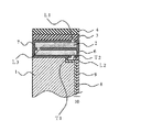
図1は本発明の超音波探触子の第一の実施例で、ケースをとりはずした状態の内部構造を構成要素の一部を切断して示した図、図2はその主要部を拡大して示した断面図である。
【0012】
図1において、1は吸音材で、例えばバリウムフェライトの粉末をゴムに混入し固めたもの、2は吸音材1の上に接着剤を用いて固着された圧電振動子で、例えばPZT圧電セラミックと、その上方向と下方向の2面及び両側面に焼き付けまたは印刷技術を用いて形成された電極とからなる。圧電振動子2は、図1のように、その横断面が矩形をしている短冊状の振動子素子をそれぞれ所定の間隔をおいて配列した構成となっている。3は第1音響整合層、4は第2音響整合層で、それぞれ振動子2の長さと同じ長さを有し、例えば、第1音響整合層3はタングステン粉末を混入したエポキシ樹脂の成形材からなり、第2音響整合層4はポリウレタン系樹脂の成形材からなり、各々の材料の超音波伝播速度から決まる波長(λ)の1/4の厚みに形成されている。5は音響レンズで、第2音響整合層4の上に接着剤で接着され、圧電振動子2から送信された超音波を振動子の配列方向と直交する面内(配列振動子の短軸方向)にて超音波をある深さに収束するものである。これらの構成は、従来の超波探触子と基本的に同様である。
【0013】
次に、本実施例の特徴的構成について図2を用いて詳述する。圧電振動子2に設けられた電極は、二つの切欠部L1およびL2により分離されて、その上面すなわち超音波放射面に設けたグランド電極7と、裏面すなわち吸音材1と対接する面に設けた信号電極6とからなっている。ここで、グランド電極7は、振動子2の上面に設けた切欠部L1から側面を通じ、裏面の一端に設けた切欠部L2に対応する部分(これを端子T1とする)までまわり込むように形成する。一方、信号電極6は、圧電振動子2の裏面の該切欠部L2に対応する部分(これを端子T2とする)でグランド電極7と分離配置され、振動子2の切欠部L1まで表面に逆にまわり込むように形成する。10は信号線9とグランド線8とを有するフレキシブル配線板であり、この配線板10のグランド線8の先端がグランド電極7の端子T1に接続され、信号線9の先端が信号電極6の端子T2に接続される。なお、本超音波探触子の製造方法については後述する。
【0014】
本実施例では、振動子2の裏面の一端で信号電極6とグランド電極7を対向配置することで、配線板10として、信号線9とグランド線8が一体構成でグランドが全面ベタの上に信号線が配置された、いわゆるマイクロストリップ線路のフレキシブル配線板が使用できるため、信号線間の電気的クロストークを小さくすることができる。
【0015】
図3は本発明の超音波探触子の第二の実施例の主要部の断面図を示すものであって、全体の構成は第一の実施例と基本的に同じ構成をとっている。第一の実施例と異なる点は、圧電振動子が二層のPZTセラミックからなり、内部電極を有する二層振動子2から構成されていることにある。この場合の信号電極とグランド電極は、三つの切欠部L1,L2,L3により分離され、振動子2の表面と裏面の両面がグランド電極7になり、内部電極が信号電極6となる。信号電極6は、振動子の表面と裏面まで側面を通じてまわり込むように形成され、特に振動子2の裏面の一端では切欠部L2によりグランド電極7と分離されている。この切欠部L2に対応するグランド電極7および信号電極6の部分を、それぞれ、端子T1およびT2とし、これら端子T1およびT2に配線板10のグランド線8の先端および信号線9の先端が接続される。
【0016】
本実施例では、配線板10は、グランド線用の全面導体と絶縁層(ポリイミド等)をはさんでその上に形成された信号線路からなった、いわゆるマイクロストリップ線路を有する配線板が用いられる。この場合も、配線板裏面の全面導体によりグランドにおとすことができるために、信号配線間のクロストークを低減させられる。また、グランドを大面積の導体により形成することができるため、グランド線を通じたクロストークも抑制される。
【0017】
図4は、本発明の超音波探触子のさらに第三の実施例の主要部の断面図を示すもので、本実施例も、全体の構成は前述の二つの実施例と基本的には同じである。異なる点は圧電振動子2として三層のPZTセラミックスからなる積層圧電体を用いている点にある。この三層振動子2の信号電極とグランド電極は切欠部L1,L2,L3,L4により分離された、振動子2の表面がグランド電極7,振動子2の裏面が信号電極6からなる。ここで、振動子2の裏面の一端における電極構造は図1と同じであり、これら電極の端子T1,T2に、配線板10のグランド線8と信号線9が接続される。本実施例においても、第一の実施例と同様のマイクロストリップ線路を有するフレキシブル配線板が使用できるため、信号線間の電気的クロストークを小さくできる。
【0018】
図5は、図2および図4に示した超音波探触子に用いられるフレキシブル配線板10の平面図であり、図6はそのA−A’線上の断面図である。本実施例は絶縁板11の上側に全面ベタの銅はくよりなるグランド線8を形成し、その下側には絶縁板11’で支持された信号線9を設ける。信号線9の先端はグランド線8の先端よりも長くなるようにする。そして、信号線9のピッチは振動子2のピッチと一致するようにする。このような配線板10を図2および図4のように振動子2に接続するには、まだ短冊状に切断されていない圧電振動子2のグランド電極7の端子T1に配線板10のグランド線8の先端を接続し、信号電極6の端子T2には配線板10の信号線9の先端を接続する。そして、振動子2を短冊状に切断するときに、同時に配線板10のグランド線8および絶縁板11,11’を一定ピッチで所定の深さCまで切断する。その結果、切断された振動子2ごとに、配線板10のグランド線8および信号線9の先端が分離した形で、それぞれ、グランド電極7および信号電極6に接続されるようになる。
【0019】
図7は図3の超音波探触子に用いられる配線板10の平面図であり、図8はそのA−A’線上の断面図である。本実施例は絶縁板11の上側に信号線9を形成し、下側には全面ベタの銅はくよりなるグランド線8を設ける。グランド線8の先端は信号線9の先端よりも長くするように形成する。信号線9のピッチは振動子2のピッチと一致するようにする。振動子との接続は、まだ切断されていない振動子2のグランド電極7の端子T1に配線板10のグランド線8の先端を接続し、信号電極6の端子T2には配線板10の信号線9を接続することで行う。短冊状の振動子2を形成するときに、同時に配線板10のグランド線8および絶縁板11の先端を一定ピッチで深さCまで切断する。
【0020】
図9は配線板10の他の実施例を示す平面図であり、図10はそのA−A’線上の断面図である。本実施例は、図5や図7に示す配線板10の信号線9の間に第二のグランド線8’を設け、これと全面ベタの第一のグランド線8とを多数のスルーホール12で接続したものである。すなわち、例えばポリイミド樹脂部材よりなる絶縁板11の表面に信号線9を形成し、その間に第二のグランド線8’を設ける。絶縁板11の裏面には全面ベタの銅はくよりなる第一のグランド線8を形成する。そして、これらグランド線8’とグランド線8とを多数のスルーホール12で接続する。このように形成された配線板10は、これまで説明してきたと同様な手法で、振動子の電極に接続され、振動子がカットされるとき、配線板の先端もカットされる。
【0021】
本実施例の配線板10では、信号線9の間にグランド線8’を挿入した構造になっている。これにより、配線板内の信号線間の電気的クロストークをいっそう小さくすることができる。なお、本実施例では、直線状の配線パターンについて説明したが、別にこれに限るわけではなく、曲線状パターンであっても良く、その信号線パターンの間にグランド線パターンが挿入されていれば良い。
【0022】
図11は配線板10のさらに他の実施例を示す平面図であり、図12はそのA−A’線上の断面図、図13はB−B’線上の断面図である。本実施例は、ポリイミド樹脂などよりなる絶縁板11のほぼ中央部に短冊状の振動子のピッチと一致したピッチで信号線9を埋め込む。そして、絶縁板11の上側と下側に、それぞれ、全面ベタの銅はくよりなるグランド線8,8”を設け、その間を多数のスルーホール12で接続する。図12および13に示すように、信号線9の先端は絶縁板11から露出され、振動子の信号電極と接続できるように形成される。この配線板10の振動子電極との接続および先端部分の切断も、これまで説明してきたと同様の手法でなされる。
【0023】
本実施例の配線板10は、銅からなる信号線9が銅箔の上下グランド8、8”にはさまれた絶縁体ポリイミド樹脂11の中に配置されたストリップライン型からなっている。本構成の配線板10を用いることにより、これまで説明した配線板と同様に信号線間の電気的クロストークを小さくすることができる。また、伝送線路の特性インピーダンスを設計することができるため、インピーダンス整合がとりやすいなどの利点も有する。
【0024】
以上の各実施例において、配線板10の振動子電極との接続先端とは反対側の後端部において、信号線とグランド線は、それぞれ、超音波装置本体に接続された同軸ケーブルの信号線およびグランド線に直接接続してもよいが、コネクタを介して同軸ケーブルに接続するのが望しい。
【0025】
図14はその実施例を説明するための接続構成ブロック図である。図において、配線板10は、例えば、図7および図8に示したものであって、その信号線の先端およびグランド線の先端は、それぞれ、振動子2の一端の信号電極およびグランド電極に接続されている。配線板10の後端部において、信号線とグランド線とは、ここでは4個のコネクタ13を介して超音波診断装置への接続用コネクタ15に接続された同軸ケーブル14に接続する。各々のコネクタ13はレセタクルとヘッダとからなり、レセタクルは配線板10に取付けられ、ヘッダは同軸ケーブル14に接続されている。図15は一つのコネクタ13のレセタクルに接続するための配線板10の後端部に設けられた配線パターンを示したものである。すなわち、配線板10の表面に信号ピン16を設け、これと信号線9とを接続する。信号ピン16の間には、グランド線ピン17を設け、スルーホール18を介して配線板10の裏面のグランド線に接続する。コネクタ13のレセタクルの端子は、これら信号ピン16およびグランドピン17に対応するように形成されて電気的に接続される。
【0026】
ここで、図5および図6に示す配線板10の後端部に図15に示した信号ピン16およびグランド17を設ける場合には、絶縁板11’の後端部を切り欠き、信号線9を露出させてそこに信号ピンを設け、その間にグランドピンを設ける。グランドピンとグランド線との接続は前記同様にスルーホールを介してなされる。また、図7および図8の配線板10に信号ピンおよびグランドピンを設ける場合には、信号線9に対応して信号ピンを設け、その間にグランドピンを設けて、裏面のグランド線をスルーホールで接続する。図9および図10の配線板10の後端板に信号ピンおよびグランドピンを設ける場合には、この後端部にはグランド線8’を設けず、信号線9のみとし、上記と同様に信号線9と信号ピンとを接続し、また、グランド線8とグランドピンとをスルーホールで接続する。
【0027】
さらに、図11〜図12の配線板10の後端部に信号ピンおよびグランドピンを設ける場合には、この端部には、グランド線8および上側の絶縁板11を切り欠いた状態に形成して信号線9を露出させてそこに信号ピンを設け、その間にグランドピンを設け、グランドピンはスルーホールを介してグランド線8”と接続すればよい。
【0028】
次に、図1および図2の実施例を参照して、本発明の超音波探触子の製造方法説明する。まず、公知の手段により、セラミック粉体を焼結してPZT圧電セラミック板を形成する(短冊状にカットされていない矩形状のセラミック板)。このセラミック板の全面にスクリーン印刷手段(公知)により電極を形成して圧電振動子とする。このとき、電極上面の片側にセラミック板の長手方向に沿って切欠部L1を設け、また、電極下面に同様の方向に沿って切欠部L2を設け、電極上面をグランド電極7とし、電極下面を信号電極6とする。また、グランド電極7および信号電極6の切欠部L2に対応する部分をそれぞれの端子T1およびT2とする。次に、図5および図6に示したような配線板10を電極に半田づけ接続する。すなわち、配線板10の信号線9の先端部分を信号電極6の端子T2に半田づけし、配線板10のグランド線8の先端部分をグランド電極7の端子T1に接続する。このように配線板10をとりつけた圧電振動子を吸音材1の上に接着材を用いて固着する。その後、圧電振動子板の前面に音響整合層3および4を接着剤を用いて固着する。以上のようにして得た積層配置した振動子板を配線板とともに所定ピッチでアレイ形状に切断加工する。その結果、振動子板は短冊状に切断され、図1に示す振動子2のように加工される。さらに、図5に示すように配線板10の先端の絶縁板11,11’およびグランド線8は点線で示したように深さCまで切断され、その信号線9およびグランド線8の各々は、それに対応する振動子2と個々に接続された状態になる。
【0029】
以上のステップにより、図1および図2に示した探触子が製造される。図3,図4に示す探触子は二層および三層の振動子を用いる点に特徴があるが、その製造方法は上記と同様である。
【0030】
【発明の効果】
以上説明したように、請求項1の発明によれば、圧電振動子をその裏面の一端において信号電極とグランド電極を分離する切欠部を設ける構造とし、該切欠部に対応する信号電極とグランド電極の部分に、一枚の配線板に絶縁体をはさんで形成された信号線とグランド線の先端部を電気的に接続することにより、配線板が信号線とグランド線が一体構成のいわゆるマイクロストリップ線路型あるいはストリップライン型構成となり、信号線間の電気的クロストークを低減できる。そして、このクロストークの低減により、S/Nの良好な特性を有する超音波探触子を提供することができる。
【0031】
また、請求項2の発明によれば、配線板上の信号線の間にもグランド線を設けたので、信号線間に発生するクロストロークをさらに低減させることができる。
また、請求項3の発明によれば、配線板を、絶縁体の内部の中央部に信号線を埋設し、絶縁板の上下面全面を銅はくよりなるグランド線とする構造としたので、特性インピーダンスの調整が可能で、インピーダンス整合をとることができるため、信号線間に発生するクロストークをさらに低減させることができる。
【0032】
さらに、請求項4の発明によれば、配線板の後端部に設けた信号ピンの間にグランドピンを設け、このグランドピンと配線板の全面銅はくとをスルーホールで接続したので、信号ピン間に発生するクロストークも低減させることができる。
【図面の簡単な説明】
【図1】本発明の超音波探触子の第一の実施例の一部を断面で示した斜視図である。
【図2】図1の主要部の構造を示す断面図である。
【図3】本発明の超音波探触子の第二の実施例の主要部の構造を示す断面図である。
【図4】本発明の超音波探触子の第三の実施例の主要部の構造を示す断面図である。
【図5】本発明の超音波探触子で用いられる配線板の一実施例の平面図である。
【図6】図5のA−A′線上の断面図である。
【図7】本発明の超音波探触子で用いられる配線板の他の実施例の平面図である。
【図8】図7のA−A′線上の断面図である。
【図9】本発明の超音波探触子で用いられる配線板の他の実施例を示す平面図である。
【図10】図9のA−A′線上の断面図である。
【図11】本発明の超音波探触子で用いられる配線板のさらに他の実施例を示す平面図である。
【図12】図11のA−A′線上の断面図である。
【図13】図11のB−B′線上の断面図である。
【図14】本発明の超音波探触子で用いられる配線板と同軸ケーブルとの接続を説明するためのブロック図である。
【図15】本発明の超音波探触子で用いられる配線板のケーブル接続用コネクタ部の配線パターンの一部を示す図である。
【符号の説明】
1 吸音材
2 圧電振動子
3 第1音響整合層
4 第2音響整合層
5 音響レンズ
6 信号電極
7 グランド電極
8 グランド線
9 信号線
10 配線板
11 絶縁板
12 スルーホール
16 信号ピン
17 グランドピン
18 スルーホール[0001]
BACKGROUND OF THE INVENTION
The present invention relates to an ultrasonic probe used in the field of an ultrasonic apparatus that renders the inside of a subject as an image using ultrasonic waves, and in particular, obtains a good ultrasonic image by reducing electrical crosstalk and the like. For technology.
[0002]
[Prior art]
Ultrasound diagnostic equipment used for medical imaging diagnosis uses ultrasonic pulse reflection method to display tomographic images of soft tissue of the living body, blood flow images in the generation, etc. on a monitor in almost real time, and radiation It is said to be safe without any exposure, and is also widely used in the medical field because it is small and inexpensive. In such an ultrasonic diagnostic apparatus, an ultrasonic probe is used to transmit ultrasonic waves into the subject and receive echo signals from within the subject.
[0003]
In general, the basic configuration of an ultrasonic probe is formed by providing a sound absorbing material on the back surface of a piezoelectric vibrator and an acoustic matching layer on an ultrasonic radiation surface. A probe used in an electronic scanning type ultrasonic apparatus is usually composed of a large number of elongated strip-shaped transducers. A plurality of the elongated strip-like vibrators are taken as a group, and each vibrator in the group is driven with a predetermined delay time. Accordingly, an ultrasonic beam that converges in a predetermined depth and in a predetermined direction in the subject is transmitted from the probe. Also, at the time of reception, an ultrasonic beam is received from a predetermined direction by giving each transducer a delay time that varies with time. Then, ultrasonic image data is obtained by moving the ultrasonic beam for transmission / reception in the array direction of the transducers and scanning the subject.
[0004]
In order to obtain a good ultrasonic image by the above scanning, it is necessary to form a thin ultrasonic beam having excellent directivity of the ultrasonic beam over the entire scanning range of the ultrasonic beam. For this purpose, electrical crosstalk between the vibrators of the array vibrator is small, and high S / N is important.
[0005]
In general, in an ultrasonic probe, a signal is applied to the electrode on the back surface of the transducer, the ultrasonic radiation surface, ie, the electrode on the front surface is grounded, and electromagnetically used as a shield electrode. In an array type ultrasonic probe in which a plurality of transducers are arranged, a wiring board is connected to each back electrode of each micro transducer element, and the elements are insulated and electrically connected. Small crosstalk is required. On the other hand, all the surface electrodes on the ultrasonic radiation surface are arranged on a common ground. Conventionally, in order to obtain such an electrode configuration, a method of separately connecting a signal applying wiring board and a common ground lead line or board to a vibrator has been employed. The wiring board and the ultrasonic apparatus main body are connected by a coaxial cable, and the wiring board and the coaxial cable are connected by a connector. In this case, conventionally, the pin pattern of the wiring board connected to the receptacle of the connector is composed of adjacent signal pins.
[0006]
[Problems to be solved by the invention]
The conventional ultrasonic probe has the following drawbacks. Since only the signal lines connected to the vibrator are wired on the wiring board, when a signal is applied, an electric field is generated between the signal lines, and the occurrence of electrical crosstalk is inevitable. Further, since the lead wire for the common ground is made of a thin copper wire, the ground is weak, which also causes electrical crosstalk between the transducer elements. Furthermore, since the connector has a configuration in which only signal pins are adjacent to each other, crosstalk also occurs between them.
[0007]
An object of the present invention is to provide an ultrasonic probe that eliminates the above-mentioned conventional drawbacks in an electronic scanning array type probe or the like in which a plurality of transducers are arranged.
[0008]
[Means for Solving the Problems]
The ultrasonic probe of the present invention includes a piezoelectric vibrator, an acoustic matching layer and an acoustic lens arranged on the ultrasonic irradiation side of the piezoelectric vibrator, a sound absorbing material arranged on the back surface of the piezoelectric vibrator, in the ultrasonic probe having at least one notch for separating the signal electrodes and the ground electrodes on the periphery of the piezoelectric vibrator, and a signal line connected to the signal electrodes, copper entire solid to be connected to the ground electrode A wiring board having first and second ground lines made of foil and an insulating board is provided, and the signal lines are embedded in the insulating board at a constant pitch that matches the pitch of the piezoelectric vibrator. And an upper surface of the tip of the signal line is formed so as to be exposed from the insulating plate and connected to the signal electrode, the first ground line is disposed on the upper surface of the insulating plate, and the lower surface of the insulating plate Second gra Lead wires are arranged, the first and the second ground line and the ground line are connected through the insulating plate.
[0009]
The wiring board has a signal pin on one surface of a rear end portion of the wiring board, and a ground pin between the signal pins, the signal line is connected to the signal pin, and the ground pin is The first ground line or the second ground line formed on the other surface of the wiring board is connected through a through hole.
[0011]
DETAILED DESCRIPTION OF THE INVENTION
Hereinafter, several examples as embodiments of the present invention will be described with reference to the drawings.
FIG. 1 is a first embodiment of an ultrasonic probe according to the present invention. FIG. 2 is a diagram showing an internal structure with a case removed, with a part of the components cut, and FIG. It is sectional drawing shown.
[0012]
In FIG. 1, 1 is a sound absorbing material, for example, barium ferrite powder mixed in rubber and hardened, 2 is a piezoelectric vibrator fixed on the sound absorbing material 1 using an adhesive, for example PZT piezoelectric ceramic and The electrodes are formed by printing or printing techniques on two upper and lower surfaces and both side surfaces thereof. As shown in FIG. 1, the
[0013]
Next, the characteristic configuration of the present embodiment will be described in detail with reference to FIG. The electrode provided on the
[0014]
In this embodiment, the
[0015]
FIG. 3 shows a cross-sectional view of the main part of the second embodiment of the ultrasonic probe of the present invention, and the overall configuration is basically the same as that of the first embodiment. The difference from the first embodiment is that the piezoelectric vibrator is made of a two-layer PZT ceramic and has a two-
[0016]
In this embodiment, the
[0017]
FIG. 4 shows a cross-sectional view of the main part of the third embodiment of the ultrasonic probe of the present invention. The overall configuration of this embodiment is basically the same as the two embodiments described above. The same. A different point is that a laminated piezoelectric body made of three layers of PZT ceramics is used as the
[0018]
FIG. 5 is a plan view of the
[0019]
FIG. 7 is a plan view of the
[0020]
FIG. 9 is a plan view showing another embodiment of the
[0021]
In the
[0022]
11 is a plan view showing still another embodiment of the
[0023]
The
[0024]
In each of the above embodiments, the signal line and the ground line at the rear end portion of the
[0025]
FIG. 14 is a connection configuration block diagram for explaining the embodiment. In the figure, the
[0026]
Here, when the
[0027]
Furthermore, when providing a signal pin and a ground pin at the rear end of the
[0028]
Next, a method for manufacturing an ultrasonic probe according to the present invention will be described with reference to the embodiment shown in FIGS. First, a PZT piezoelectric ceramic plate is formed by sintering ceramic powder by a known means (a rectangular ceramic plate not cut into a strip shape). Electrodes are formed on the entire surface of the ceramic plate by screen printing means (known) to form a piezoelectric vibrator. At this time, a notch L1 is provided along the longitudinal direction of the ceramic plate on one side of the upper surface of the electrode, and a notch L2 is provided along the same direction on the lower surface of the electrode. The
[0029]
Through the above steps, the probe shown in FIGS. 1 and 2 is manufactured. The probe shown in FIGS. 3 and 4 is characterized in that it uses two-layer and three-layer transducers, but its manufacturing method is the same as described above.
[0030]
【The invention's effect】
As described above, according to the first aspect of the present invention, the piezoelectric vibrator has a structure in which the notch for separating the signal electrode and the ground electrode is provided at one end of the back surface, and the signal electrode and the ground electrode corresponding to the notch are provided. In this part, the signal line formed by sandwiching an insulator between a single wiring board and the tip of the ground line are electrically connected to each other so that the wiring board is integrated with the signal line and the ground line. It becomes a stripline type or stripline type configuration, and electrical crosstalk between signal lines can be reduced. By reducing the crosstalk, an ultrasonic probe having a good S / N characteristic can be provided.
[0031]
According to the invention of
According to the invention of
[0032]
Further, according to the invention of
[Brief description of the drawings]
FIG. 1 is a perspective view showing a part of a first embodiment of an ultrasonic probe of the present invention in section.
2 is a cross-sectional view showing the structure of the main part of FIG.
FIG. 3 is a cross-sectional view showing the structure of the main part of a second embodiment of the ultrasonic probe of the present invention.
FIG. 4 is a sectional view showing the structure of the main part of a third embodiment of the ultrasonic probe of the present invention.
FIG. 5 is a plan view of an embodiment of a wiring board used in the ultrasonic probe of the present invention.
6 is a cross-sectional view taken along the line AA ′ of FIG.
FIG. 7 is a plan view of another embodiment of a wiring board used in the ultrasonic probe of the present invention.
8 is a cross-sectional view taken along line AA ′ of FIG.
FIG. 9 is a plan view showing another embodiment of a wiring board used in the ultrasonic probe of the present invention.
10 is a cross-sectional view taken along the line AA ′ in FIG. 9;
FIG. 11 is a plan view showing still another embodiment of a wiring board used in the ultrasonic probe of the present invention.
12 is a cross-sectional view taken along the line AA ′ of FIG.
13 is a cross-sectional view taken along the line BB ′ of FIG.
FIG. 14 is a block diagram for explaining a connection between a wiring board and a coaxial cable used in the ultrasonic probe of the present invention.
FIG. 15 is a view showing a part of a wiring pattern of a cable connecting connector portion of a wiring board used in the ultrasonic probe of the present invention.
[Explanation of symbols]
DESCRIPTION OF SYMBOLS 1
Claims (2)
前記信号電極に接続する信号線と、前記グランド電極に接続する全面ベタの銅はくよりなる第1のグランド線及び第2のグランド線と、絶縁板とを有する配線板を備え、
前記信号線は前記絶縁板内部に前記圧電振動子のピッチと一致した一定のピッチで埋め込まれ、前記信号線の先端の上面は前記絶縁板から露出され前記信号電極と接続できるように形成され、
前記絶縁板の上面に前記第1のグランド線が配置され、前記絶縁板の下面に前記第2のグランド線が配置され、前記第1のグランド線と前記第2のグランド線は前記絶縁板を貫通して接続されることを特徴とする超音波探触子。A piezoelectric vibrator, an acoustic matching layer and an acoustic lens disposed on the ultrasonic wave irradiation side of the piezoelectric vibrator, a sound absorbing material disposed on the back surface of the piezoelectric vibrator, and a signal electrode and a periphery of the piezoelectric vibrator In an ultrasonic probe having at least one notch separating the ground electrode,
Includes a signal line connected to the signal electrode, the first ground line and the second ground line comprising a copper foil of whole-area solid to be connected to the ground electrode, a wiring board having an insulating plate,
The signal line is embedded in the insulating plate at a constant pitch that matches the pitch of the piezoelectric vibrator, and the upper surface of the tip of the signal line is exposed from the insulating plate and can be connected to the signal electrode,
The first ground line is disposed on an upper surface of the insulating plate, the second ground line is disposed on a lower surface of the insulating plate, and the first ground line and the second ground line are disposed on the insulating plate. An ultrasonic probe characterized by being connected through.
Priority Applications (1)
| Application Number | Priority Date | Filing Date | Title |
|---|---|---|---|
| JP09135797A JP3934202B2 (en) | 1997-03-27 | 1997-03-27 | Ultrasonic probe |
Applications Claiming Priority (1)
| Application Number | Priority Date | Filing Date | Title |
|---|---|---|---|
| JP09135797A JP3934202B2 (en) | 1997-03-27 | 1997-03-27 | Ultrasonic probe |
Publications (2)
| Publication Number | Publication Date |
|---|---|
| JPH10262968A JPH10262968A (en) | 1998-10-06 |
| JP3934202B2 true JP3934202B2 (en) | 2007-06-20 |
Family
ID=14024144
Family Applications (1)
| Application Number | Title | Priority Date | Filing Date |
|---|---|---|---|
| JP09135797A Expired - Fee Related JP3934202B2 (en) | 1997-03-27 | 1997-03-27 | Ultrasonic probe |
Country Status (1)
| Country | Link |
|---|---|
| JP (1) | JP3934202B2 (en) |
Families Citing this family (4)
| Publication number | Priority date | Publication date | Assignee | Title |
|---|---|---|---|---|
| US6552471B1 (en) * | 1999-01-28 | 2003-04-22 | Parallel Design, Inc. | Multi-piezoelectric layer ultrasonic transducer for medical imaging |
| WO2003086196A1 (en) | 2002-04-17 | 2003-10-23 | Hitachi Medical Corporation | Ultrasonic probe in body cavity |
| JP4812050B2 (en) * | 2004-12-17 | 2011-11-09 | 株式会社日立メディコ | Ultrasonic probe and ultrasonic diagnostic apparatus using the same |
| KR101068918B1 (en) | 2009-06-23 | 2011-09-30 | 삼성메디슨 주식회사 | Transducer for ultrasonic diagnosis device and method for manufaturing the same |
Family Cites Families (4)
| Publication number | Priority date | Publication date | Assignee | Title |
|---|---|---|---|---|
| JPS643557A (en) * | 1987-06-26 | 1989-01-09 | Toshiba Corp | Ultrasonic probe |
| JPH04347146A (en) * | 1991-05-27 | 1992-12-02 | Toshiba Corp | Ultrasonic probe |
| JP2724102B2 (en) * | 1993-12-28 | 1998-03-09 | ケル株式会社 | 2-layer flexible printed circuit board |
| JPH07212043A (en) * | 1994-01-20 | 1995-08-11 | Hitachi Cable Ltd | Printed wiring board and multi-wire wiring board |
-
1997
- 1997-03-27 JP JP09135797A patent/JP3934202B2/en not_active Expired - Fee Related
Also Published As
| Publication number | Publication date |
|---|---|
| JPH10262968A (en) | 1998-10-06 |
Similar Documents
| Publication | Publication Date | Title |
|---|---|---|
| US6308389B1 (en) | Ultrasonic transducer and manufacturing method therefor | |
| US6936008B2 (en) | Ultrasound system with cableless coupling assembly | |
| US5957850A (en) | Multi-array pencil-sized ultrasound transducer and method of imaging and manufacture | |
| EP1436097B1 (en) | System for attaching an acoustic element to an integrated circuit | |
| EP1728563B1 (en) | Ultrasonic probe and ultrasonic probe manufacturing method | |
| US6497667B1 (en) | Ultrasonic probe using ribbon cable attachment system | |
| US9603580B2 (en) | High frequency ultrasound probe | |
| CA2139151A1 (en) | Two-dimensional acoustic array and method for the manufacture thereof | |
| CN110026329B (en) | Ultrasonic transducer and preparation method thereof | |
| JP3288815B2 (en) | 2D array ultrasonic probe | |
| JP2007142555A (en) | Ultrasonic probe and ultrasonic diagnostic equipment | |
| US7249513B1 (en) | Ultrasound probe | |
| JP3934202B2 (en) | Ultrasonic probe | |
| EP2883429B1 (en) | Ultrasound endoscope and methods of manufacture thereof | |
| JP2002224104A (en) | Ultrasonic array vibrator | |
| JP3469386B2 (en) | Ultrasonic transducer and method of manufacturing the same | |
| JP3029931B2 (en) | Ultrasonic transducer manufacturing method | |
| JPH11347032A (en) | Ultrasonic probe | |
| JPS58118739A (en) | Ultasonic probe and production thereof | |
| JP3325368B2 (en) | Ultrasonic probe and manufacturing method thereof | |
| JP7049323B2 (en) | Flexible circuit with redundant connection points for ultrasonic arrays | |
| CN113333261A (en) | High-frequency array transducer | |
| JPH05123317A (en) | Two-dimensional array ultrasonic probe | |
| JPH04179074A (en) | Method for connecting multi-core cable | |
| KR102623559B1 (en) | Ultrasound prove |
Legal Events
| Date | Code | Title | Description |
|---|---|---|---|
| A521 | Written amendment |
Free format text: JAPANESE INTERMEDIATE CODE: A523 Effective date: 20040303 |
|
| A621 | Written request for application examination |
Free format text: JAPANESE INTERMEDIATE CODE: A621 Effective date: 20040303 |
|
| A977 | Report on retrieval |
Free format text: JAPANESE INTERMEDIATE CODE: A971007 Effective date: 20060707 |
|
| A131 | Notification of reasons for refusal |
Free format text: JAPANESE INTERMEDIATE CODE: A131 Effective date: 20060724 |
|
| A521 | Written amendment |
Free format text: JAPANESE INTERMEDIATE CODE: A523 Effective date: 20060915 |
|
| A131 | Notification of reasons for refusal |
Free format text: JAPANESE INTERMEDIATE CODE: A131 Effective date: 20061212 |
|
| A521 | Written amendment |
Free format text: JAPANESE INTERMEDIATE CODE: A523 Effective date: 20070208 |
|
| TRDD | Decision of grant or rejection written | ||
| A01 | Written decision to grant a patent or to grant a registration (utility model) |
Free format text: JAPANESE INTERMEDIATE CODE: A01 Effective date: 20070312 |
|
| A61 | First payment of annual fees (during grant procedure) |
Free format text: JAPANESE INTERMEDIATE CODE: A61 Effective date: 20070315 |
|
| R150 | Certificate of patent (=grant) or registration of utility model |
Free format text: JAPANESE INTERMEDIATE CODE: R150 |
|
| FPAY | Renewal fee payment (event date is renewal date of database) |
Free format text: PAYMENT UNTIL: 20110330 Year of fee payment: 4 |
|
| FPAY | Renewal fee payment (event date is renewal date of database) |
Free format text: PAYMENT UNTIL: 20110330 Year of fee payment: 4 |
|
| FPAY | Renewal fee payment (event date is renewal date of database) |
Free format text: PAYMENT UNTIL: 20130330 Year of fee payment: 6 |
|
| FPAY | Renewal fee payment (event date is renewal date of database) |
Free format text: PAYMENT UNTIL: 20140330 Year of fee payment: 7 |
|
| LAPS | Cancellation because of no payment of annual fees |