EP2883429B1 - Ultrasound endoscope and methods of manufacture thereof - Google Patents
Ultrasound endoscope and methods of manufacture thereof Download PDFInfo
- Publication number
- EP2883429B1 EP2883429B1 EP13827230.7A EP13827230A EP2883429B1 EP 2883429 B1 EP2883429 B1 EP 2883429B1 EP 13827230 A EP13827230 A EP 13827230A EP 2883429 B1 EP2883429 B1 EP 2883429B1
- Authority
- EP
- European Patent Office
- Prior art keywords
- printed circuit
- circuit board
- bonding pads
- vias
- ultrasound
- Prior art date
- Legal status (The legal status is an assumption and is not a legal conclusion. Google has not performed a legal analysis and makes no representation as to the accuracy of the status listed.)
- Active
Links
- 238000002604 ultrasonography Methods 0.000 title claims description 45
- 238000000034 method Methods 0.000 title claims description 26
- 238000004519 manufacturing process Methods 0.000 title description 12
- 239000000463 material Substances 0.000 claims description 23
- 239000004020 conductor Substances 0.000 claims description 19
- 239000000523 sample Substances 0.000 claims description 11
- 238000005520 cutting process Methods 0.000 claims description 8
- 239000004593 Epoxy Substances 0.000 claims description 7
- 238000004891 communication Methods 0.000 claims description 6
- 229910052751 metal Inorganic materials 0.000 claims description 2
- 239000002184 metal Substances 0.000 claims description 2
- 238000003491 array Methods 0.000 description 6
- 238000005452 bending Methods 0.000 description 3
- 238000003384 imaging method Methods 0.000 description 3
- 229910052782 aluminium Inorganic materials 0.000 description 2
- XAGFODPZIPBFFR-UHFFFAOYSA-N aluminium Chemical compound [Al] XAGFODPZIPBFFR-UHFFFAOYSA-N 0.000 description 2
- 229910052451 lead zirconate titanate Inorganic materials 0.000 description 2
- 239000000758 substrate Substances 0.000 description 2
- RYGMFSIKBFXOCR-UHFFFAOYSA-N Copper Chemical compound [Cu] RYGMFSIKBFXOCR-UHFFFAOYSA-N 0.000 description 1
- PWHULOQIROXLJO-UHFFFAOYSA-N Manganese Chemical compound [Mn] PWHULOQIROXLJO-UHFFFAOYSA-N 0.000 description 1
- 230000002745 absorbent Effects 0.000 description 1
- 239000002250 absorbent Substances 0.000 description 1
- PNEYBMLMFCGWSK-UHFFFAOYSA-N aluminium oxide Inorganic materials [O-2].[O-2].[O-2].[Al+3].[Al+3] PNEYBMLMFCGWSK-UHFFFAOYSA-N 0.000 description 1
- 239000000919 ceramic Substances 0.000 description 1
- 229910052802 copper Inorganic materials 0.000 description 1
- 239000010949 copper Substances 0.000 description 1
- NKZSPGSOXYXWQA-UHFFFAOYSA-N dioxido(oxo)titanium;lead(2+) Chemical compound [Pb+2].[O-][Ti]([O-])=O NKZSPGSOXYXWQA-UHFFFAOYSA-N 0.000 description 1
- 238000009558 endoscopic ultrasound Methods 0.000 description 1
- 239000011152 fibreglass Substances 0.000 description 1
- 239000010408 film Substances 0.000 description 1
- 229920005570 flexible polymer Polymers 0.000 description 1
- 230000009969 flowable effect Effects 0.000 description 1
- HFGPZNIAWCZYJU-UHFFFAOYSA-N lead zirconate titanate Chemical compound [O-2].[O-2].[O-2].[O-2].[O-2].[Ti+4].[Zr+4].[Pb+2] HFGPZNIAWCZYJU-UHFFFAOYSA-N 0.000 description 1
- 229910052748 manganese Inorganic materials 0.000 description 1
- 239000011572 manganese Substances 0.000 description 1
- 238000005259 measurement Methods 0.000 description 1
- 238000001465 metallisation Methods 0.000 description 1
- 239000000203 mixture Substances 0.000 description 1
- 238000004806 packaging method and process Methods 0.000 description 1
- 238000001020 plasma etching Methods 0.000 description 1
- 239000000843 powder Substances 0.000 description 1
- 238000000926 separation method Methods 0.000 description 1
- 239000007787 solid Substances 0.000 description 1
- 239000006104 solid solution Substances 0.000 description 1
- 125000006850 spacer group Chemical group 0.000 description 1
- 239000010409 thin film Substances 0.000 description 1
- 230000000699 topical effect Effects 0.000 description 1
Images


Classifications
-
- A—HUMAN NECESSITIES
- A61—MEDICAL OR VETERINARY SCIENCE; HYGIENE
- A61B—DIAGNOSIS; SURGERY; IDENTIFICATION
- A61B8/00—Diagnosis using ultrasonic, sonic or infrasonic waves
- A61B8/12—Diagnosis using ultrasonic, sonic or infrasonic waves in body cavities or body tracts, e.g. by using catheters
-
- A—HUMAN NECESSITIES
- A61—MEDICAL OR VETERINARY SCIENCE; HYGIENE
- A61B—DIAGNOSIS; SURGERY; IDENTIFICATION
- A61B8/00—Diagnosis using ultrasonic, sonic or infrasonic waves
- A61B8/44—Constructional features of the ultrasonic, sonic or infrasonic diagnostic device
- A61B8/4483—Constructional features of the ultrasonic, sonic or infrasonic diagnostic device characterised by features of the ultrasound transducer
- A61B8/4488—Constructional features of the ultrasonic, sonic or infrasonic diagnostic device characterised by features of the ultrasound transducer the transducer being a phased array
-
- H—ELECTRICITY
- H05—ELECTRIC TECHNIQUES NOT OTHERWISE PROVIDED FOR
- H05K—PRINTED CIRCUITS; CASINGS OR CONSTRUCTIONAL DETAILS OF ELECTRIC APPARATUS; MANUFACTURE OF ASSEMBLAGES OF ELECTRICAL COMPONENTS
- H05K1/00—Printed circuits
- H05K1/18—Printed circuits structurally associated with non-printed electric components
- H05K1/189—Printed circuits structurally associated with non-printed electric components characterised by the use of a flexible or folded printed circuit
-
- H—ELECTRICITY
- H05—ELECTRIC TECHNIQUES NOT OTHERWISE PROVIDED FOR
- H05K—PRINTED CIRCUITS; CASINGS OR CONSTRUCTIONAL DETAILS OF ELECTRIC APPARATUS; MANUFACTURE OF ASSEMBLAGES OF ELECTRICAL COMPONENTS
- H05K3/00—Apparatus or processes for manufacturing printed circuits
- H05K3/40—Forming printed elements for providing electric connections to or between printed circuits
- H05K3/403—Edge contacts; Windows or holes in the substrate having plural connections on the walls thereof
-
- H—ELECTRICITY
- H05—ELECTRIC TECHNIQUES NOT OTHERWISE PROVIDED FOR
- H05K—PRINTED CIRCUITS; CASINGS OR CONSTRUCTIONAL DETAILS OF ELECTRIC APPARATUS; MANUFACTURE OF ASSEMBLAGES OF ELECTRICAL COMPONENTS
- H05K2203/00—Indexing scheme relating to apparatus or processes for manufacturing printed circuits covered by H05K3/00
- H05K2203/04—Soldering or other types of metallurgic bonding
- H05K2203/049—Wire bonding
-
- H—ELECTRICITY
- H05—ELECTRIC TECHNIQUES NOT OTHERWISE PROVIDED FOR
- H05K—PRINTED CIRCUITS; CASINGS OR CONSTRUCTIONAL DETAILS OF ELECTRIC APPARATUS; MANUFACTURE OF ASSEMBLAGES OF ELECTRICAL COMPONENTS
- H05K3/00—Apparatus or processes for manufacturing printed circuits
- H05K3/0011—Working of insulating substrates or insulating layers
- H05K3/0044—Mechanical working of the substrate, e.g. drilling or punching
- H05K3/0052—Depaneling, i.e. dividing a panel into circuit boards; Working of the edges of circuit boards
-
- Y—GENERAL TAGGING OF NEW TECHNOLOGICAL DEVELOPMENTS; GENERAL TAGGING OF CROSS-SECTIONAL TECHNOLOGIES SPANNING OVER SEVERAL SECTIONS OF THE IPC; TECHNICAL SUBJECTS COVERED BY FORMER USPC CROSS-REFERENCE ART COLLECTIONS [XRACs] AND DIGESTS
- Y10—TECHNICAL SUBJECTS COVERED BY FORMER USPC
- Y10T—TECHNICAL SUBJECTS COVERED BY FORMER US CLASSIFICATION
- Y10T29/00—Metal working
- Y10T29/49—Method of mechanical manufacture
- Y10T29/49002—Electrical device making
- Y10T29/49117—Conductor or circuit manufacturing
- Y10T29/49124—On flat or curved insulated base, e.g., printed circuit, etc.
- Y10T29/49147—Assembling terminal to base
- Y10T29/49151—Assembling terminal to base by deforming or shaping
-
- Y—GENERAL TAGGING OF NEW TECHNOLOGICAL DEVELOPMENTS; GENERAL TAGGING OF CROSS-SECTIONAL TECHNOLOGIES SPANNING OVER SEVERAL SECTIONS OF THE IPC; TECHNICAL SUBJECTS COVERED BY FORMER USPC CROSS-REFERENCE ART COLLECTIONS [XRACs] AND DIGESTS
- Y10—TECHNICAL SUBJECTS COVERED BY FORMER USPC
- Y10T—TECHNICAL SUBJECTS COVERED BY FORMER US CLASSIFICATION
- Y10T29/00—Metal working
- Y10T29/49—Method of mechanical manufacture
- Y10T29/49002—Electrical device making
- Y10T29/49117—Conductor or circuit manufacturing
- Y10T29/49124—On flat or curved insulated base, e.g., printed circuit, etc.
- Y10T29/49155—Manufacturing circuit on or in base
- Y10T29/49165—Manufacturing circuit on or in base by forming conductive walled aperture in base
Definitions
- Array-based endoscopic ultrasound systems operating at frequencies in the 1-10MHz range are used frequently for laparoscopic imaging where they provide fast scanning rates, dynamic focusing and beam steering.
- ultrasound arrays For endoscopic imaging applications requiring higher resolution such as intravascular, intracardiac, transurethral, trans-nasal and transtympanic imaging, ultrasound arrays have been challenging to manufacture owing the small element size, small element pitch and need to package the finished endoscope into a small enough package to enter the required lumens.
- These applications have, therefore, been served mainly by single element ultrasound endoscopes which, compared to arrays, suffer slower frame rates, a tradeoff between depth of field and lateral resolution and the necessity of having moving parts in the endoscope head which adds bulk and causes unwanted vibrations.
- Piel et al. (US 6,541,896 B1 ) describes a combined acoustic backing and interconnect module for connecting an array of ultrasonic transducer elements to a multiplicity of conductors of a cable, utilizing the backing layer volume to extend a high density of interconnections perpendicular to the transducer array surface.
- the module is made by injecting flowable backfill material into a mold made up of a plurality of spacer plates having aligned channels, with interleaved flexible circuit boards. The backfill material is cured to form a backing layer which supports the flexible circuit boards in mutually parallel relationship.
- Excess flexible circuit material on one side of the backing layer is cut flush with the front face of the backing layer, leaving exposed ends of the conductive traces on the flexible circuit boards.
- the module is then laminated to a piezoelectric ceramic layer, and diced.
- the flexible circuit board conductive traces are aligned with, and electrically connected to, signal electrodes of the transducer elements.
- the other ends of the conductive traces on a fanout portion of the flexible circuit board are connected to the cable.
- Lucas et al. (US 2007/0222339 A1 ) describes an ultrasonic transducer comprising a stack having a plurality of layers, each layer having a top surface and an opposed bottom surface, wherein the plurality of layers of the stack comprises an upper unpoled piezoelectric layer, an underlying lower poled piezoelectric layer, and a dielectric layer.
- the dielectric layer is connected to the piezoelectric layer and defines an opening extending a second predetermined length in a direction substantially parallel to the axis of the stack.
- a plurality of first kerf slots are defined therein the stack, each first kerf slot extending a predetermined depth therein the stack through the upper piezoelectric layer and into the lower piezoelectric layer and a first predetermined length in a direction substantially parallel to the axis.
- Dausch et al. (WO 2012/075153 A2 ) describes an ultrasound device including an ultrasonic transducer device having a plurality of transducer elements forming a transducer array.
- Each transducer element includes a piezoelectric material disposed between a first electrode and a second electrode.
- One of the first and second electrodes is a ground electrode and the other of the first and second electrodes is a signal electrode.
- the ultrasound device further includes a cable assembly having a plurality of connective signal elements and a plurality of connective ground elements extending in substantially parallel relation therealong.
- Each connective element is configured to form an electrically-conductive engagement with respective ones of the signal electrodes and the ground electrodes of the transducer elements in the transducer array.
- the connective ground elements are alternatingly disposed with the connective signal elements across the cable assembly, to provide shielding between the connective signal elements.
- an ultrasonic array has piezoelectric material and a plurality of electrodes. Each electrode is electrically connected to a respective signal wire, and the plurality of signal wires are embedded in a printed circuit board, the board having an angle of greater than about 60 degrees with respect to the array.
- an ultrasound device in accordance with appended claims 1 - 9.
- a method of electrically connecting an ultrasound array to a printed circuit board in accordance with appended claims 10 - 14.
- the configuration described above is included in an endoscope.
- the angle can be greater than 70 degrees.
- the angle can be greater than 80 degrees.
- the angle can be approximately 90 degrees.
- the printed circuit board can be a flexible circuit.
- a method of manufacture of any of the above includes creating vias in the printed circuit board and cutting the vias transversely to expose conductive material at the edge of the board.
- the array is then wire bonded to the conductive material, such that the material acts as a wire bonding pad.
- Other implementations are possible, such as generally when the array is electrically connected to the conductive material by thin metal film, conductive epoxy, or the like.
- the cutting can be accomplished by a dicing saw or by similar methods.
- the cutting can be accomplished by a laser.
- an ultrasonic array has piezoelectric material and a plurality of electrodes. Each electrode is correspondingly electrically connected to one of a plurality of signal wires, the wires having an angle of greater than about 60 degrees with respect to the array. In certain implementations, the angle can be greater than 70 degrees. The angle can be greater than 80 degrees. The angle can be approximately 90 degrees.
- a method of manufacture of approximately perpendicular wire bonds includes creating vias in a flexible circuit and cutting the vias transversely to expose conductive material at the edge of the flexible circuit.
- a method of manufacture of electrical connections between an ultrasonic array and a printed circuit board includes creating vias in the board and cutting the vias transversely to expose the conductive material at the edge of the board.
- an ultrasound device comprising:
- An array with an electrical harness (such as flex or PCB or series of conductors) may be set a defined angle relative to a stack. There may be no bend required.
- the volumetric footprint can be minimized as well as the number of components.
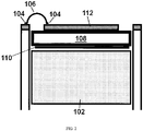
- a surface of piezoelectric material 108 is systematically electroded with electrodes 110, such that it defines an array 112 of individual elements that transmit and receive acoustic signals.
- Piezoelectric materials such as lead zirconate titanate (PZT) or lead manganese niobate in solid solution with lead titanate (PMNx-PT(1-x)) are often used.
- kerfs cuts made into the piezoelectric material 108 are made using a saw, laser, reactive ion etching or other methods.
- Each element in the array 112 is electrically connected (generally by way of a wire bonding pad) to a wire 106, which is correspondingly electrically connected on its other end by wire bonding pads 104 on a printed circuit board 100.
- Signal wires (not shown) embedded in the printed circuit board 100 are electrically connected to each pad 104, and send each signal from each element to the distal end of the probe (this is the end which is mechanically manipulated by a clinician).
- the printed circuit board is a flexible (flex) circuit, which packages many of signal wires composed of conductive material by sandwiching them between flexible polymer layers.
- Printed circuit board 100 could also be inflexible, in which the insulating layers may be FR-4 fiberglass.
- a flex circuit 100 is approximately parallel to the surface of the array 112 for a significant distance before bending away from the probe end.
- the smallest dimension possible for such an endoscope is limited by how much of the flex circuit remains at the probe end.
- bonding pads 104 are exposed on both the flex circuit 100 and the array 112, and wires 106 are used to attach array pads and flex circuit pads to each other.
- the manufacturer specifies a minimum bend radius, often on the order of a few millimeters for a multilayer flex circuit such as those used to carry ultrasound array signals.
- This minimum bend radius requires that the flex circuit extend laterally from the ultrasound array for several millimeters before bending back, which greatly increases the cross-sectional area of the device. It is possible, in some embodiments, that no other structures are needed for mechanical support. In some embodiments, attachment may also be made to wires carried in another structure; if such structure is attached so that the wires meet the plane of the array surface, then a minimum bend radius may be required to avoid damaging such wires. Since the minimum size of a lumen into which the endoscope can enter is limited by the endoscope's cross-sectional area it is desirable to reduce the cross-sectional area as much as possible.
- FIGs. 2 and 3 We now turn to an embodiment of the endoscope of the present invention; see FIGs. 2 and 3 .
- the flex circuits are wire bonded (or otherwise electrically connected) approximately normal to the array surface.
- the flex circuit does not bend, and the cross-sectional probe area need only be large enough to accommodate the array elements, bonding pads, and the thickness of the flex circuit at the probe end.
- This arrangement can be used in a variety of applications, including endoscopic high-frequency phased array ultrasound systems, non-endoscopic high-frequency ultrasound phased arrays, and both endoscopic and non-endoscopic phased and linear ultrasound arrays.
- an endoscope of the present invention comprises a 40 MHz, 64-element phased array transducer packaged into a 2.47 mm by 2.42 mm endoscopic form factor, in which the array is a forward looking kerfless design based on PMN-32%PT with an element-to-element pitch of 38 microns.
- the angle of the flex circuit with respect to the array is approximately 90 degrees. In some embodiments, the angle of the flex circuit with respect to the array is between 80 and 90 degrees. In some embodiments, the angle of the flex circuit with respect to the array is between 70 and 90 degrees. In some embodiments, the angle of the flex circuit with respect to the array is between about 60 and 90 degrees. In some embodiments crossing the normal plane, the angle of the flex circuit with respect to the array may exceed 90 degrees.
- Attaching a printed circuit board approximately perpendicular to an array creates a manufacturing challenge because wire bonds between the array and the printed circuit board must connect to the board edge-on.
- flex circuitry is built by attaching together laminar layers, thus bonding pads cannot easily be mounted on the edge of a flex circuit.
- wire bonds are usually made between two parallel surfaces, it is difficult to make connections to bonding pads on the surface of a printed circuit board in this configuration, whether it is flexible or inflexible.
- This method enables wire bonding of signal wires to array elements; electrical connection is also possible using conductive epoxy or thin film metal deposition.
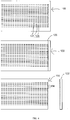
- the method of manufacture includes the following steps (see FIG. 4 ).
- a set of filled partial vias 126 is formed in the printed circuit board 100 ( FIG. 4 top). These vias correspond to the position of the embedded signal wires 128, which are composed of conductive material suitable for electrical connections.
- this procedure is performed twice such that the vias 126 are arranged in two rows through the depth of the printed circuit board 100, with one row through the top two layers and one through the bottom two layers such that they alternate.
- the board is then cut across its width with a dicing saw so as to cut the vias 126 in half near the edge of the board ( FIG. 4 middle), exposing conductive material 124 corresponding to each signal wire at the site of the cut 120 ( FIG. 4 bottom).
- the array substrate was a 2.4mm by 2.4 mm piece of PMN-32%PT lapped to 47 um thickness.
- An array of 64 electrodes was photolithographically defined on the top surface of this substrate with an electrode width of 27 um and an element-to-element pitch of 37 um.
- Each electrode was fanned out to a bonding pad arranged in two rows on each side of the array (four rows total).
- a 1.2 um layer of aluminum was sputtered onto the back side of the array to define a ground electrode, and a thick layer of conductive epoxy was attached to it to act as an absorbent acoustic backing layer. This epoxy was removed with a dicing saw in order to avoid making the bonding pads piezoelectrically active.
- Two 6-layer flex circuit boards were designed to connect to the elements from either side of the array. Each flex circuit had 32 traces terminating at individual copper-filled vias near the end of the board. The flex circuits were cut through the middle of the solid vias using a dicing saw. The two flex circuit boards were epoxied onto opposite sides of the transducer stack such that the diced vias were aligned with the bonding pads fanned out from the array. A jig was then machined to hold the flex + transducer stack upright in front of the wire-bonding tool. 15-micron thick aluminum wire bonds were used to connect the bonding pads on the array to the diced vias within the thickness of the array.
- wirebonds were encapsulated with a thick insulating epoxy consisting of a 30% by volume mixture of Alumina powder and Epotek 301 (Epotek) insulating epoxy.
- a matching layer/lens combination was then epoxied onto the front face of the endoscope.
- Micro-coaxial cables were directly soldered to the flex circuit at the distal end of the probe.
Landscapes
- Health & Medical Sciences (AREA)
- Life Sciences & Earth Sciences (AREA)
- Engineering & Computer Science (AREA)
- Pathology (AREA)
- General Health & Medical Sciences (AREA)
- Physics & Mathematics (AREA)
- Surgery (AREA)
- Public Health (AREA)
- Biophysics (AREA)
- Radiology & Medical Imaging (AREA)
- Biomedical Technology (AREA)
- Heart & Thoracic Surgery (AREA)
- Medical Informatics (AREA)
- Molecular Biology (AREA)
- Veterinary Medicine (AREA)
- Animal Behavior & Ethology (AREA)
- Nuclear Medicine, Radiotherapy & Molecular Imaging (AREA)
- Microelectronics & Electronic Packaging (AREA)
- Gynecology & Obstetrics (AREA)
- Manufacturing & Machinery (AREA)
- Ultra Sonic Daignosis Equipment (AREA)
- Chemical & Material Sciences (AREA)
- Analytical Chemistry (AREA)
- Biochemistry (AREA)
- General Physics & Mathematics (AREA)
- Immunology (AREA)
- Investigating Or Analyzing Materials By The Use Of Ultrasonic Waves (AREA)
- Endoscopes (AREA)
Description
- Array-based endoscopic ultrasound systems operating at frequencies in the 1-10MHz range are used frequently for laparoscopic imaging where they provide fast scanning rates, dynamic focusing and beam steering. For endoscopic imaging applications requiring higher resolution such as intravascular, intracardiac, transurethral, trans-nasal and transtympanic imaging, ultrasound arrays have been challenging to manufacture owing the small element size, small element pitch and need to package the finished endoscope into a small enough package to enter the required lumens. These applications have, therefore, been served mainly by single element ultrasound endoscopes which, compared to arrays, suffer slower frame rates, a tradeoff between depth of field and lateral resolution and the necessity of having moving parts in the endoscope head which adds bulk and causes unwanted vibrations.
- In recent years there has been significant progress in developing fully sampled forward looking high frequency linear array transducers. For most applications a phase-array endoscope would offer significant improvements over a single-element endoscope. However, although the elements are conventionally proportioned in these arrays, the overall packaging of the transducers remains relatively large. This limits the application of the arrays to topical use where images are generated from outside the body.
-
Piel et al. (US 6,541,896 B1 ) describes a combined acoustic backing and interconnect module for connecting an array of ultrasonic transducer elements to a multiplicity of conductors of a cable, utilizing the backing layer volume to extend a high density of interconnections perpendicular to the transducer array surface. The module is made by injecting flowable backfill material into a mold made up of a plurality of spacer plates having aligned channels, with interleaved flexible circuit boards. The backfill material is cured to form a backing layer which supports the flexible circuit boards in mutually parallel relationship. Excess flexible circuit material on one side of the backing layer is cut flush with the front face of the backing layer, leaving exposed ends of the conductive traces on the flexible circuit boards. The module is then laminated to a piezoelectric ceramic layer, and diced. The flexible circuit board conductive traces are aligned with, and electrically connected to, signal electrodes of the transducer elements. The other ends of the conductive traces on a fanout portion of the flexible circuit board are connected to the cable. -
Lucas et al. (US 2007/0222339 A1 ) describes an ultrasonic transducer comprising a stack having a plurality of layers, each layer having a top surface and an opposed bottom surface, wherein the plurality of layers of the stack comprises an upper unpoled piezoelectric layer, an underlying lower poled piezoelectric layer, and a dielectric layer. The dielectric layer is connected to the piezoelectric layer and defines an opening extending a second predetermined length in a direction substantially parallel to the axis of the stack. A plurality of first kerf slots are defined therein the stack, each first kerf slot extending a predetermined depth therein the stack through the upper piezoelectric layer and into the lower piezoelectric layer and a first predetermined length in a direction substantially parallel to the axis. -
Dausch et al. (WO 2012/075153 A2 ) describes an ultrasound device including an ultrasonic transducer device having a plurality of transducer elements forming a transducer array. Each transducer element includes a piezoelectric material disposed between a first electrode and a second electrode. One of the first and second electrodes is a ground electrode and the other of the first and second electrodes is a signal electrode. The ultrasound device further includes a cable assembly having a plurality of connective signal elements and a plurality of connective ground elements extending in substantially parallel relation therealong. Each connective element is configured to form an electrically-conductive engagement with respective ones of the signal electrodes and the ground electrodes of the transducer elements in the transducer array. The connective ground elements are alternatingly disposed with the connective signal elements across the cable assembly, to provide shielding between the connective signal elements. - In general, in an aspect, an ultrasonic array has piezoelectric material and a plurality of electrodes. Each electrode is electrically connected to a respective signal wire, and the plurality of signal wires are embedded in a printed circuit board, the board having an angle of greater than about 60 degrees with respect to the array.
- In one aspect, there is provided an ultrasound device in accordance with appended claims 1 - 9. In another aspect, there is provided a method of electrically connecting an ultrasound array to a printed circuit board, in accordance with appended claims 10 - 14. In certain implementations, the configuration described above is included in an endoscope. The angle can be greater than 70 degrees. The angle can be greater than 80 degrees. The angle can be approximately 90 degrees. The printed circuit board can be a flexible circuit.
- In general, in an aspect, a method of manufacture of any of the above includes creating vias in the printed circuit board and cutting the vias transversely to expose conductive material at the edge of the board. In certain implementations, the array is then wire bonded to the conductive material, such that the material acts as a wire bonding pad. Other implementations are possible, such as generally when the array is electrically connected to the conductive material by thin metal film, conductive epoxy, or the like. The cutting can be accomplished by a dicing saw or by similar methods. The cutting can be accomplished by a laser.
- In general, in an aspect, an ultrasonic array has piezoelectric material and a plurality of electrodes. Each electrode is correspondingly electrically connected to one of a plurality of signal wires, the wires having an angle of greater than about 60 degrees with respect to the array. In certain implementations, the angle can be greater than 70 degrees. The angle can be greater than 80 degrees. The angle can be approximately 90 degrees.
- In general, in an aspect, a method of manufacture of approximately perpendicular wire bonds includes creating vias in a flexible circuit and cutting the vias transversely to expose conductive material at the edge of the flexible circuit.
- In general, in an aspect, a method of manufacture of electrical connections between an ultrasonic array and a printed circuit board includes creating vias in the board and cutting the vias transversely to expose the conductive material at the edge of the board.
- These and other features and aspects, and combinations of them, maybe expressed as methods, systems, components, means and steps for performing functions, business methods, program products, and in other ways.
- Other advantages and features will become apparent from the following description and from the claims.
- In one aspect, there is provided an ultrasound device comprising:
- a transducer stack comprising a piezoelectric material, said piezoelectric material comprising a top surface, a plurality of side surfaces;
- a plurality of electrodes formed on said top surface, said plurality of electrodes defining elements of an ultrasound array, wherein each electrode is in electrical communication with a respective ultrasound array bonding pad; and
- a printed circuit board comprising a plurality of signal wires embedded therein, wherein an end portion thereof is provided adjacent to a first side surface of said transducer stack such that an angle between said printed circuit board and the top surface of said piezoelectric material is at least 60 degrees, and wherein an edge thereof is aligned with said top surface;
- wherein electrical connections are provided between said ultrasound array bonding pads and electrically conductive material exposed in said edge of said printed circuit board such that each electrode is electrically connected to a respective signal wire.
- In another aspect, there is provided a method of electrically connecting an ultrasound array to a printed circuit board, the printed circuit board comprising a plurality of signal wires embedded therein, the method comprising:
- providing a transducer stack comprising a piezoelectric material and a plurality of electrodes, wherein said piezoelectric material comprises a top surface, a plurality of side surfaces, wherein said plurality of electrodes are formed on said top surface such that said plurality of electrodes define elements of said ultrasound array, and wherein each electrode is in electrical communication with a respective ultrasound array bonding pad;
- cutting the printed circuit board transversely to form an edge of the printed circuit board exposing conductive material at the edge;
- providing the printed circuit board such that an end portion thereof is adjacent to a first side surface of said transducer stack, and such that an angle between said printed circuit board and the top surface of said piezoelectric material is at least 60 degrees, and such that an edge thereof is aligned with said top surface; and
- forming electrical connections between the ultrasound array bonding pads and electrically conductive material exposed in said edge of said printed circuit board such that each electrode is electrically connected to a respective signal wire.
-
-
FIG. 1 shows a partial perspective view of the probe end of a conventional endoscope. -
FIG. 2 shows a sectional view of the probe end of an endoscope of the present invention. -
FIG. 3 shows a partial perspective view of the probe end of an endoscope of the present invention. -
FIG. 4 depicts steps, from top to bottom, in the method of manufacture of the present invention. -
FIG. 5 shows a graph of impedance in ohms at 10 MHz vs array element number for the endoscope of the Example. -
- 100 Flex circuit, printed circuit board
- 102 Transducer stack, backing
- 104 Wire bonding pads
- 106 Wire to/from array element
- 108 Piezoelectric material
- 110 Electrodes
- 112 Array, ultrasonic array
- 120 Cut
- 122 Discarded half of the board edge
- 124 Exposed conductive material at the board edge
- 126 Via
- 128 Signal wire
- Miniaturized high-frequency, ultrasonic phased array endoscopes have been successfully designed and fabricated. An array with an electrical harness (such as flex or PCB or series of conductors) may be set a defined angle relative to a stack. There may be no bend required. The volumetric footprint can be minimized as well as the number of components.
- The advantages of an endoscope of this invention, as well as methods of manufacture of such endoscopes, can be seen by contrast to a conventional endoscope design in
FIG. 1 . At the probe end, a surface ofpiezoelectric material 108 is systematically electroded withelectrodes 110, such that it defines anarray 112 of individual elements that transmit and receive acoustic signals. Piezoelectric materials such as lead zirconate titanate (PZT) or lead manganese niobate in solid solution with lead titanate (PMNx-PT(1-x)) are often used. To achieve additional separation between elements, in some cases kerfs (cuts made into the piezoelectric material 108) are made using a saw, laser, reactive ion etching or other methods. Each element in thearray 112 is electrically connected (generally by way of a wire bonding pad) to awire 106, which is correspondingly electrically connected on its other end bywire bonding pads 104 on a printedcircuit board 100. Signal wires (not shown) embedded in the printedcircuit board 100 are electrically connected to eachpad 104, and send each signal from each element to the distal end of the probe (this is the end which is mechanically manipulated by a clinician). Often, the printed circuit board is a flexible (flex) circuit, which packages many of signal wires composed of conductive material by sandwiching them between flexible polymer layers. Printedcircuit board 100 could also be inflexible, in which the insulating layers may be FR-4 fiberglass. - Note that in the conventional endoscope design of
FIG. 1 , aflex circuit 100 is approximately parallel to the surface of thearray 112 for a significant distance before bending away from the probe end. The smallest dimension possible for such an endoscope is limited by how much of the flex circuit remains at the probe end. Typically,bonding pads 104 are exposed on both theflex circuit 100 and thearray 112, andwires 106 are used to attach array pads and flex circuit pads to each other. In order to prevent damage to theflex circuit 100, the manufacturer specifies a minimum bend radius, often on the order of a few millimeters for a multilayer flex circuit such as those used to carry ultrasound array signals. This minimum bend radius requires that the flex circuit extend laterally from the ultrasound array for several millimeters before bending back, which greatly increases the cross-sectional area of the device. It is possible, in some embodiments, that no other structures are needed for mechanical support. In some embodiments, attachment may also be made to wires carried in another structure; if such structure is attached so that the wires meet the plane of the array surface, then a minimum bend radius may be required to avoid damaging such wires. Since the minimum size of a lumen into which the endoscope can enter is limited by the endoscope's cross-sectional area it is desirable to reduce the cross-sectional area as much as possible. - We now turn to an embodiment of the endoscope of the present invention; see
FIGs. 2 and3 . Rather than have a printed circuit board 100 (such as a flex circuit) wire bonded approximately parallel to the surface of anarray 112, instead the flex circuits are wire bonded (or otherwise electrically connected) approximately normal to the array surface. In such an arrangement the flex circuit does not bend, and the cross-sectional probe area need only be large enough to accommodate the array elements, bonding pads, and the thickness of the flex circuit at the probe end. This arrangement can be used in a variety of applications, including endoscopic high-frequency phased array ultrasound systems, non-endoscopic high-frequency ultrasound phased arrays, and both endoscopic and non-endoscopic phased and linear ultrasound arrays. In some embodiments, an endoscope of the present invention comprises a 40 MHz, 64-element phased array transducer packaged into a 2.47 mm by 2.42 mm endoscopic form factor, in which the array is a forward looking kerfless design based on PMN-32%PT with an element-to-element pitch of 38 microns. In some embodiments, the angle of the flex circuit with respect to the array is approximately 90 degrees. In some embodiments, the angle of the flex circuit with respect to the array is between 80 and 90 degrees. In some embodiments, the angle of the flex circuit with respect to the array is between 70 and 90 degrees. In some embodiments, the angle of the flex circuit with respect to the array is between about 60 and 90 degrees. In some embodiments crossing the normal plane, the angle of the flex circuit with respect to the array may exceed 90 degrees. - Attaching a printed circuit board approximately perpendicular to an array creates a manufacturing challenge because wire bonds between the array and the printed circuit board must connect to the board edge-on. In particular, flex circuitry is built by attaching together laminar layers, thus bonding pads cannot easily be mounted on the edge of a flex circuit. Moreover, because wire bonds are usually made between two parallel surfaces, it is difficult to make connections to bonding pads on the surface of a printed circuit board in this configuration, whether it is flexible or inflexible. The present invention solves these challenges by providing a novel method of manufacture. In some embodiments, this method enables wire bonding of signal wires to array elements; electrical connection is also possible using conductive epoxy or thin film metal deposition.
- In a wire bonding embodiment, the method of manufacture includes the following steps (see
FIG. 4 ). A set of filled partial vias 126 is formed in the printed circuit board 100 (FIG. 4 top). These vias correspond to the position of the embedded signal wires 128, which are composed of conductive material suitable for electrical connections. In some embodiments, this procedure is performed twice such that the vias 126 are arranged in two rows through the depth of the printedcircuit board 100, with one row through the top two layers and one through the bottom two layers such that they alternate. The board is then cut across its width with a dicing saw so as to cut the vias 126 in half near the edge of the board (FIG. 4 middle), exposingconductive material 124 corresponding to each signal wire at the site of the cut 120 (FIG. 4 bottom). Theremainder 122 is discarded. In methods of manufacture of endoscopes of the present invention, wire bonds are then made between anarray 112 and the cut vias 126 in the board, thus allowing a connection to be made without introducing any bending in the printed circuit board. - See below for an example of endoscopes of the present invention constructed using a method of manufacture of the present invention.
- The array substrate was a 2.4mm by 2.4 mm piece of PMN-32%PT lapped to 47 um thickness. An array of 64 electrodes was photolithographically defined on the top surface of this substrate with an electrode width of 27 um and an element-to-element pitch of 37 um. Each electrode was fanned out to a bonding pad arranged in two rows on each side of the array (four rows total). A 1.2 um layer of aluminum was sputtered onto the back side of the array to define a ground electrode, and a thick layer of conductive epoxy was attached to it to act as an absorbent acoustic backing layer. This epoxy was removed with a dicing saw in order to avoid making the bonding pads piezoelectrically active. Two 6-layer flex circuit boards were designed to connect to the elements from either side of the array. Each flex circuit had 32 traces terminating at individual copper-filled vias near the end of the board. The flex circuits were cut through the middle of the solid vias using a dicing saw. The two flex circuit boards were epoxied onto opposite sides of the transducer stack such that the diced vias were aligned with the bonding pads fanned out from the array. A jig was then machined to hold the flex + transducer stack upright in front of the wire-bonding tool. 15-micron thick aluminum wire bonds were used to connect the bonding pads on the array to the diced vias within the thickness of the array. The wirebonds were encapsulated with a thick insulating epoxy consisting of a 30% by volume mixture of Alumina powder and Epotek 301 (Epotek) insulating epoxy. A matching layer/lens combination was then epoxied onto the front face of the endoscope. Micro-coaxial cables were directly soldered to the flex circuit at the distal end of the probe.
- Measurements of the impedance of the elements (see
FIG. 5 ) measured from the distal end of the flex circuit show that this technique does indeed provide a good electrical connection to the transducer elements, with low impedance electrical connections in the wire bond between the flex circuit and the array.
Claims (14)
- An ultrasonic device comprising:a transducer stack (102) comprising a piezoelectric material (108), said piezoelectric material (108) comprising a top surface, a plurality of side surfaces;a plurality of electrodes (110) and a plurality of ultrasound array bonding pads formed on said top surface, said plurality of electrodes (110) defining elements of an ultrasound array (112), wherein each electrode (110) is in electrical communication with a respective ultrasound array bonding pad (104); andcharacterized in thatsaid ultrasonic device further comprises a printed circuit board (100) comprising a plurality of signal wires (128) embedded therein, wherein said printed circuit board comprises a lateral surface and a plurality of side edges, wherein an end portion of the printed circuit board is provided adjacent to a first side surface of said transducer stack (102) such that an angle between said lateral surface of said printed circuit board (100) and the top surface of said piezoelectric material (108) is at least 60 degrees and wherein an side edge of said printed circuit board is aligned with said top surface;wherein the ultrasonic device further comprises electrical connections provided between said ultrasound array bonding pads (104) and electrically conductive material (124) exposed in said edge of said printed circuit board (100) such that each electrode (110) is electrically connected to a respective signal wire (128).
- The ultrasound device according to claim 1 wherein said printed circuit board (100) comprises:a set of vias (126) formed at an end of said printed circuit board (100), such that the vias (126) intersect respective signal wires (128) within said printed circuit board (100), said vias (126) extend at least partially through said printed circuit board (100);wherein said vias (126) are filled with the electrically conductive material (124); andwherein said vias (126) are exposed in said edge of said printed circuit board (100), forming a plurality of bonding pads (104) in said edge.
- The ultrasound device according to claim 2 wherein said end portion of said printed circuit board (100) is parallel to said first side surface of said transducer stack (102).
- The ultrasound device according to claim 2 or 3 wherein said printed circuit board (100) is positioned relative to said transducer stack (102) such that said edge of said printed circuit board (100) is approximately coplanar with said ultrasound array bonding pads (104).
- The ultrasound device according to any one of claims 2 to 4 wherein said printed circuit board (100) is adhered to said first side surface of said transducer stack (102).
- The apparatus of any of claims 2 to 5 wherein said printed circuit board (100) is flexible.
- The ultrasound device according to claim 2 wherein said printed circuit board (100) is a first printed circuit board, said plurality of electrodes (110) are a plurality of first electrodes, said plurality of signal wires (128) are a plurality of first signal wires, said plurality of bonding pads are a plurality of first bonding pads, said ultrasound device further comprising a plurality of second electrodes spatially interleaved with said plurality of first electrodes, said plurality of second electrodes defining additional elements of said ultrasound array (112), said ultrasound array bonding pads (104) comprise first ultrasound array bonding pads and second ultrasound array bonding pads, said ultrasound device further comprising a second printed circuit board;said second printed circuit board comprising a plurality of second signal wires embedded therein, wherein an edge of said second printed circuit board comprises a plurality of second bonding pads, each second bonding pad being in electrical communication with a respective second signal wire;wherein an end portion of said second printed circuit board is provided adjacent to a second side surface of said transducer stack (102), wherein an angle between said end portion of said second printed circuit board and said top surface is at least 60 degrees;wherein electrical connections are provided between said second bonding pads of said second printed circuit boards and said second ultrasound array bonding pads such that each second electrode is electrically connected to a respective second signal wire; andwherein said first printed circuit board and said second printed circuit boards are provided on opposite sides of said transducer stack (102).
- The ultrasound device according to any one of claims 2 to 7, wherein the electrical connections are formed by wire bonding.
- An ultrasound probe comprising an ultrasound device according to any one of claims 2 to 8.
- A method of electrically connecting an ultrasound array (112) to a printed circuit board (100), the printed circuit board (100) comprising a plurality of signal wires (128) embedded therein, the method comprising:providing a transducer stack (102) comprising a piezoelectric material (108) and a plurality of electrodes (110), wherein said piezoelectric material (108) comprises a top surface, a plurality of side surfaces, wherein said plurality of electrodes (110) are formed on said top surface such that said plurality of electrodes (110) define elements of said ultrasound array (112), and wherein each electrode (110) is in electrical communication with a respective ultrasound array bonding pad (104);cutting the printed circuit board (100) transversely to form an edge on the side of the lateral surface of the printed circuit board (100) exposing conductive material (124) at the edge;providing the printed circuit board (100) such that an end portion thereof is adjacent to a first side surface of said transducer stack (102), and such that an angle between said lateral surface of said printed circuit board (100) and the top surface of said piezoelectric material (108) is at least 60 degrees, and such that an edge of said printed circuit board is aligned with said top surface; andforming electrical connections between the ultrasound array bonding pads (104) and electrically conductive material (124) exposed in said edge of said printed circuit board (100) such that each electrode (110) is electrically connected to a respective signal wire (128).
- The method according to claim 10 wherein the following steps are performed prior to cutting the printed circuit board (100):forming a set of vias (126) within the printed circuit board (100), such that the vias (126) intersect respective signal wires (128) that are embedded within the printed circuit board (100);filling the vias (126) with an electrically conductive material (124), thereby forming a set of filled vias (126) within the printed circuit board (100); andwherein the printed circuit board (100) is cut transversely through the set of filled vias (126) to form an edge of the printed circuit board (100), such that the set of filled vias (126) are cut to form a plurality of bonding pads and to expose the plurality of bonding pads at the edge, wherein the bonding pads are in electrical communication with respective signal wires (128) within the printed circuit board (100); andwherein the electrical connections are formed between the ultrasound array bonding pads and the bonding pads such that each electrode (110) is electrically connected to a respective signal wire (128).
- The method according to claim 10 or 11 wherein the electrical connection are formed by wire bonding.
- The method according to claim 10 or 11 wherein the electrical connections are formed by thin metal film or conductive epoxy.
- The method according to claim 11 wherein the vias (126) are arranged in two rows through the depth of the printed circuit board (100), wherein one row of vias (126) extends through two top layers of the printed circuit board (100), and the other row of vias (126) extends through two bottom layers of the printed circuit board (100), and wherein the vias (126) in the two rows are formed such that they alternate.
Applications Claiming Priority (3)
| Application Number | Priority Date | Filing Date | Title |
|---|---|---|---|
| US201261681320P | 2012-08-09 | 2012-08-09 | |
| US201261710696P | 2012-10-06 | 2012-10-06 | |
| PCT/CA2013/050613 WO2014022938A1 (en) | 2012-08-09 | 2013-08-09 | Ultrasound endoscope and methods of manufacture thereof |
Publications (3)
| Publication Number | Publication Date |
|---|---|
| EP2883429A1 EP2883429A1 (en) | 2015-06-17 |
| EP2883429A4 EP2883429A4 (en) | 2016-07-20 |
| EP2883429B1 true EP2883429B1 (en) | 2019-05-15 |
Family
ID=50067341
Family Applications (1)
| Application Number | Title | Priority Date | Filing Date |
|---|---|---|---|
| EP13827230.7A Active EP2883429B1 (en) | 2012-08-09 | 2013-08-09 | Ultrasound endoscope and methods of manufacture thereof |
Country Status (7)
| Country | Link |
|---|---|
| US (2) | US10149660B2 (en) |
| EP (1) | EP2883429B1 (en) |
| JP (1) | JP6261581B2 (en) |
| CN (1) | CN104663006B (en) |
| CA (1) | CA2880652C (en) |
| HK (1) | HK1211778A1 (en) |
| WO (1) | WO2014022938A1 (en) |
Families Citing this family (3)
| Publication number | Priority date | Publication date | Assignee | Title |
|---|---|---|---|---|
| US11717140B2 (en) | 2015-06-24 | 2023-08-08 | The Regents Of The University Of Colorado, A Body Corporate | Multi-use endoscope with integrated device-patient monitoring and patient-provider positioning and disassociation system |
| CA3004356C (en) * | 2015-11-25 | 2024-04-23 | Fujifilm Sonosite, Inc. | Medical instrument including high frequency ultrasound transducer array |
| WO2019041040A1 (en) | 2017-09-01 | 2019-03-07 | Dalhousie University | Transducer assembly for generating focused ultrasound |
Family Cites Families (27)
| Publication number | Priority date | Publication date | Assignee | Title |
|---|---|---|---|---|
| JPH0543770Y2 (en) * | 1986-03-14 | 1993-11-05 | ||
| JPH06105842A (en) * | 1992-05-22 | 1994-04-19 | Toshiba Corp | Ultrasonic trasducer |
| US5465724A (en) * | 1993-05-28 | 1995-11-14 | Acuson Corporation | Compact rotationally steerable ultrasound transducer |
| DE4325028B4 (en) * | 1993-07-26 | 2005-05-19 | Siemens Ag | Ultrasonic transducer device comprising a one or two dimensional array of transducer elements |
| JP3526486B2 (en) * | 1995-04-28 | 2004-05-17 | 株式会社東芝 | Ultrasonic probe, ultrasonic probe equipped with the probe, and methods of manufacturing these |
| US5810009A (en) * | 1994-09-27 | 1998-09-22 | Kabushiki Kaisha Toshiba | Ultrasonic probe, ultrasonic probe device having the ultrasonic probe, and method of manufacturing the ultrasonic probe |
| US5559388A (en) * | 1995-03-03 | 1996-09-24 | General Electric Company | High density interconnect for an ultrasonic phased array and method for making |
| US5857974A (en) * | 1997-01-08 | 1999-01-12 | Endosonics Corporation | High resolution intravascular ultrasound transducer assembly having a flexible substrate |
| US6043590A (en) * | 1997-04-18 | 2000-03-28 | Atl Ultrasound | Composite transducer with connective backing block |
| JPH11155859A (en) * | 1997-09-24 | 1999-06-15 | Toshiba Corp | Ultrasonic probe and ultrasonograph using the same |
| US6541896B1 (en) | 1997-12-29 | 2003-04-01 | General Electric Company | Method for manufacturing combined acoustic backing and interconnect module for ultrasonic array |
| JP4468599B2 (en) | 2001-02-20 | 2010-05-26 | オリンパス株式会社 | Ultrasonic probe |
| US6822376B2 (en) | 2002-11-19 | 2004-11-23 | General Electric Company | Method for making electrical connection to ultrasonic transducer |
| US20070222339A1 (en) * | 2004-04-20 | 2007-09-27 | Mark Lukacs | Arrayed ultrasonic transducer |
| JP4969456B2 (en) * | 2005-01-11 | 2012-07-04 | コーニンクレッカ フィリップス エレクトロニクス エヌ ヴィ | Redistribution interconnect for microbeamformers and medical ultrasound systems |
| DE602005025257D1 (en) * | 2005-01-18 | 2011-01-20 | Esaote Spa | Ultrasonic probe, in particular for diagnostic imaging |
| JP4289304B2 (en) * | 2005-02-07 | 2009-07-01 | ブラザー工業株式会社 | Piezoelectric actuator, inkjet printer head, and manufacturing method thereof |
| KR100771862B1 (en) * | 2005-08-12 | 2007-11-01 | 삼성전자주식회사 | Manufacturing method and structure of PCB, and memory module-socket assembly |
| JP4351229B2 (en) * | 2006-06-28 | 2009-10-28 | ジーイー・メディカル・システムズ・グローバル・テクノロジー・カンパニー・エルエルシー | Manufacturing method of ultrasonic probe |
| US7834522B2 (en) * | 2007-08-03 | 2010-11-16 | Mr Holdings (Hk) Limited | Diagnostic ultrasound transducer |
| CA2713691A1 (en) * | 2008-02-05 | 2009-08-13 | Cook Ireland Ltd. | Adaptor for endoscopic orientation of an elongate medical device |
| KR20110053922A (en) * | 2008-04-21 | 2011-05-24 | 스미토모 베이클리트 컴퍼니 리미티드 | Flexible wiring unit and electronic device |
| KR101397100B1 (en) * | 2010-06-28 | 2014-05-20 | 삼성전자주식회사 | Ultrasound Probe and Manufacturing Method the same |
| EP2646173A2 (en) | 2010-12-03 | 2013-10-09 | Research Triangle Institute | Ultrasound device, and associated cable assembly |
| US8841931B2 (en) * | 2011-01-27 | 2014-09-23 | Taiwan Semiconductor Manufacturing Company, Ltd. | Probe card wiring structure |
| US20130100775A1 (en) * | 2011-10-25 | 2013-04-25 | Matthew Todd Spigelmyer | System and method for providing discrete ground connections for individual elements in an ultrasonic array transducer |
| CN105409144B (en) * | 2013-05-24 | 2019-05-03 | 富士胶片索诺声公司 | High frequency ultrasound probe |
-
2013
- 2013-08-09 US US14/420,452 patent/US10149660B2/en active Active
- 2013-08-09 CA CA2880652A patent/CA2880652C/en active Active
- 2013-08-09 CN CN201380042291.4A patent/CN104663006B/en active Active
- 2013-08-09 JP JP2015525701A patent/JP6261581B2/en active Active
- 2013-08-09 EP EP13827230.7A patent/EP2883429B1/en active Active
- 2013-08-09 WO PCT/CA2013/050613 patent/WO2014022938A1/en active Application Filing
-
2015
- 2015-12-15 HK HK15112309.4A patent/HK1211778A1/en unknown
-
2018
- 2018-12-03 US US16/207,502 patent/US20190110773A1/en not_active Abandoned
Non-Patent Citations (1)
| Title |
|---|
| None * |
Also Published As
| Publication number | Publication date |
|---|---|
| CN104663006A (en) | 2015-05-27 |
| US10149660B2 (en) | 2018-12-11 |
| CN104663006B (en) | 2019-01-15 |
| WO2014022938A1 (en) | 2014-02-13 |
| US20150209005A1 (en) | 2015-07-30 |
| US20190110773A1 (en) | 2019-04-18 |
| CA2880652C (en) | 2021-10-26 |
| HK1211778A1 (en) | 2016-05-27 |
| EP2883429A1 (en) | 2015-06-17 |
| JP2015524318A (en) | 2015-08-24 |
| CA2880652A1 (en) | 2014-02-13 |
| JP6261581B2 (en) | 2018-01-17 |
| EP2883429A4 (en) | 2016-07-20 |
Similar Documents
| Publication | Publication Date | Title |
|---|---|---|
| US7567016B2 (en) | Multi-dimensional ultrasound transducer array | |
| JP5591549B2 (en) | Ultrasonic transducer, ultrasonic probe, and method of manufacturing ultrasonic transducer | |
| US9184370B2 (en) | Ultrasonic transducer device, ultrasonic measurement apparatus, head unit, probe, and ultrasonic imaging apparatus | |
| US7288069B2 (en) | Ultrasonic probe and method of manufacturing the same | |
| US5311095A (en) | Ultrasonic transducer array | |
| US7148607B2 (en) | Ultrasonic probe and manufacturing method thereof | |
| CN102497938B (en) | Ultrasound imaging transducer acoustic stack with integral electrical connections | |
| CN103300883B (en) | Ultrasound probe and the manufacture method of ultrasound probe | |
| US9321082B2 (en) | Ultrasonic transducer, manufacturing method thereof, and ultrasonic probe | |
| KR20140004667A (en) | Ultrasound device, and associated cable assembly | |
| JP5095593B2 (en) | Ultrasonic probe and manufacturing method thereof | |
| JP4519259B2 (en) | Two-dimensional array ultrasonic probe and manufacturing method thereof | |
| US20190110773A1 (en) | Ultrasound endoscope and methods of manufacture thereof | |
| JP3288815B2 (en) | 2D array ultrasonic probe | |
| JP2005210245A (en) | Ultrasonic probe | |
| KR101491801B1 (en) | Ultrasonic transducer and method of manufacturing the same | |
| JP5454890B2 (en) | Ultrasonic probe and method for manufacturing ultrasonic probe | |
| JP4769127B2 (en) | Ultrasonic probe and ultrasonic probe manufacturing method | |
| JP3934202B2 (en) | Ultrasonic probe | |
| JP4071084B2 (en) | Manufacturing method of two-dimensional array ultrasonic probe | |
| KR20230119723A (en) | Multi-transducer chip ultrasound device |
Legal Events
| Date | Code | Title | Description |
|---|---|---|---|
| PUAI | Public reference made under article 153(3) epc to a published international application that has entered the european phase |
Free format text: ORIGINAL CODE: 0009012 |
|
| 17P | Request for examination filed |
Effective date: 20150305 |
|
| AK | Designated contracting states |
Kind code of ref document: A1 Designated state(s): AL AT BE BG CH CY CZ DE DK EE ES FI FR GB GR HR HU IE IS IT LI LT LU LV MC MK MT NL NO PL PT RO RS SE SI SK SM TR |
|
| AX | Request for extension of the european patent |
Extension state: BA ME |
|
| DAX | Request for extension of the european patent (deleted) | ||
| RIC1 | Information provided on ipc code assigned before grant |
Ipc: H05K 3/32 20060101AFI20160216BHEP Ipc: A61B 8/12 20060101ALI20160216BHEP Ipc: H05K 3/42 20060101ALI20160216BHEP Ipc: G01S 7/52 20060101ALI20160216BHEP Ipc: G01S 15/89 20060101ALI20160216BHEP |
|
| REG | Reference to a national code |
Ref country code: HK Ref legal event code: DE Ref document number: 1211778 Country of ref document: HK |
|
| RA4 | Supplementary search report drawn up and despatched (corrected) |
Effective date: 20160620 |
|
| RIC1 | Information provided on ipc code assigned before grant |
Ipc: G01S 15/89 20060101ALI20160614BHEP Ipc: H05K 3/42 20060101ALI20160614BHEP Ipc: A61B 8/12 20060101ALI20160614BHEP Ipc: H05K 3/32 20060101AFI20160614BHEP Ipc: G01S 7/52 20060101ALI20160614BHEP |
|
| STAA | Information on the status of an ep patent application or granted ep patent |
Free format text: STATUS: EXAMINATION IS IN PROGRESS |
|
| 17Q | First examination report despatched |
Effective date: 20180122 |
|
| GRAP | Despatch of communication of intention to grant a patent |
Free format text: ORIGINAL CODE: EPIDOSNIGR1 |
|
| STAA | Information on the status of an ep patent application or granted ep patent |
Free format text: STATUS: GRANT OF PATENT IS INTENDED |
|
| INTG | Intention to grant announced |
Effective date: 20181127 |
|
| GRAS | Grant fee paid |
Free format text: ORIGINAL CODE: EPIDOSNIGR3 |
|
| GRAA | (expected) grant |
Free format text: ORIGINAL CODE: 0009210 |
|
| STAA | Information on the status of an ep patent application or granted ep patent |
Free format text: STATUS: THE PATENT HAS BEEN GRANTED |
|
| AK | Designated contracting states |
Kind code of ref document: B1 Designated state(s): AL AT BE BG CH CY CZ DE DK EE ES FI FR GB GR HR HU IE IS IT LI LT LU LV MC MK MT NL NO PL PT RO RS SE SI SK SM TR |
|
| REG | Reference to a national code |
Ref country code: CH Ref legal event code: EP |
|
| REG | Reference to a national code |
Ref country code: DE Ref legal event code: R096 Ref document number: 602013055537 Country of ref document: DE |
|
| REG | Reference to a national code |
Ref country code: IE Ref legal event code: FG4D |
|
| REG | Reference to a national code |
Ref country code: CH Ref legal event code: NV Representative=s name: DR. ALEXANDER MILLER, LL.M. RECHTSANWALT (D), CH |
|
| REG | Reference to a national code |
Ref country code: NL Ref legal event code: MP Effective date: 20190515 |
|
| REG | Reference to a national code |
Ref country code: LT Ref legal event code: MG4D |
|
| PG25 | Lapsed in a contracting state [announced via postgrant information from national office to epo] |
Ref country code: NO Free format text: LAPSE BECAUSE OF FAILURE TO SUBMIT A TRANSLATION OF THE DESCRIPTION OR TO PAY THE FEE WITHIN THE PRESCRIBED TIME-LIMIT Effective date: 20190815 Ref country code: LT Free format text: LAPSE BECAUSE OF FAILURE TO SUBMIT A TRANSLATION OF THE DESCRIPTION OR TO PAY THE FEE WITHIN THE PRESCRIBED TIME-LIMIT Effective date: 20190515 Ref country code: FI Free format text: LAPSE BECAUSE OF FAILURE TO SUBMIT A TRANSLATION OF THE DESCRIPTION OR TO PAY THE FEE WITHIN THE PRESCRIBED TIME-LIMIT Effective date: 20190515 Ref country code: NL Free format text: LAPSE BECAUSE OF FAILURE TO SUBMIT A TRANSLATION OF THE DESCRIPTION OR TO PAY THE FEE WITHIN THE PRESCRIBED TIME-LIMIT Effective date: 20190515 Ref country code: AL Free format text: LAPSE BECAUSE OF FAILURE TO SUBMIT A TRANSLATION OF THE DESCRIPTION OR TO PAY THE FEE WITHIN THE PRESCRIBED TIME-LIMIT Effective date: 20190515 Ref country code: PT Free format text: LAPSE BECAUSE OF FAILURE TO SUBMIT A TRANSLATION OF THE DESCRIPTION OR TO PAY THE FEE WITHIN THE PRESCRIBED TIME-LIMIT Effective date: 20190915 Ref country code: ES Free format text: LAPSE BECAUSE OF FAILURE TO SUBMIT A TRANSLATION OF THE DESCRIPTION OR TO PAY THE FEE WITHIN THE PRESCRIBED TIME-LIMIT Effective date: 20190515 Ref country code: SE Free format text: LAPSE BECAUSE OF FAILURE TO SUBMIT A TRANSLATION OF THE DESCRIPTION OR TO PAY THE FEE WITHIN THE PRESCRIBED TIME-LIMIT Effective date: 20190515 Ref country code: HR Free format text: LAPSE BECAUSE OF FAILURE TO SUBMIT A TRANSLATION OF THE DESCRIPTION OR TO PAY THE FEE WITHIN THE PRESCRIBED TIME-LIMIT Effective date: 20190515 |
|
| PG25 | Lapsed in a contracting state [announced via postgrant information from national office to epo] |
Ref country code: RS Free format text: LAPSE BECAUSE OF FAILURE TO SUBMIT A TRANSLATION OF THE DESCRIPTION OR TO PAY THE FEE WITHIN THE PRESCRIBED TIME-LIMIT Effective date: 20190515 Ref country code: LV Free format text: LAPSE BECAUSE OF FAILURE TO SUBMIT A TRANSLATION OF THE DESCRIPTION OR TO PAY THE FEE WITHIN THE PRESCRIBED TIME-LIMIT Effective date: 20190515 Ref country code: GR Free format text: LAPSE BECAUSE OF FAILURE TO SUBMIT A TRANSLATION OF THE DESCRIPTION OR TO PAY THE FEE WITHIN THE PRESCRIBED TIME-LIMIT Effective date: 20190816 Ref country code: BG Free format text: LAPSE BECAUSE OF FAILURE TO SUBMIT A TRANSLATION OF THE DESCRIPTION OR TO PAY THE FEE WITHIN THE PRESCRIBED TIME-LIMIT Effective date: 20190815 |
|
| REG | Reference to a national code |
Ref country code: AT Ref legal event code: MK05 Ref document number: 1134924 Country of ref document: AT Kind code of ref document: T Effective date: 20190515 |
|
| PG25 | Lapsed in a contracting state [announced via postgrant information from national office to epo] |
Ref country code: SK Free format text: LAPSE BECAUSE OF FAILURE TO SUBMIT A TRANSLATION OF THE DESCRIPTION OR TO PAY THE FEE WITHIN THE PRESCRIBED TIME-LIMIT Effective date: 20190515 Ref country code: EE Free format text: LAPSE BECAUSE OF FAILURE TO SUBMIT A TRANSLATION OF THE DESCRIPTION OR TO PAY THE FEE WITHIN THE PRESCRIBED TIME-LIMIT Effective date: 20190515 Ref country code: CZ Free format text: LAPSE BECAUSE OF FAILURE TO SUBMIT A TRANSLATION OF THE DESCRIPTION OR TO PAY THE FEE WITHIN THE PRESCRIBED TIME-LIMIT Effective date: 20190515 Ref country code: RO Free format text: LAPSE BECAUSE OF FAILURE TO SUBMIT A TRANSLATION OF THE DESCRIPTION OR TO PAY THE FEE WITHIN THE PRESCRIBED TIME-LIMIT Effective date: 20190515 Ref country code: DK Free format text: LAPSE BECAUSE OF FAILURE TO SUBMIT A TRANSLATION OF THE DESCRIPTION OR TO PAY THE FEE WITHIN THE PRESCRIBED TIME-LIMIT Effective date: 20190515 Ref country code: AT Free format text: LAPSE BECAUSE OF FAILURE TO SUBMIT A TRANSLATION OF THE DESCRIPTION OR TO PAY THE FEE WITHIN THE PRESCRIBED TIME-LIMIT Effective date: 20190515 |
|
| REG | Reference to a national code |
Ref country code: DE Ref legal event code: R097 Ref document number: 602013055537 Country of ref document: DE |
|
| PG25 | Lapsed in a contracting state [announced via postgrant information from national office to epo] |
Ref country code: SM Free format text: LAPSE BECAUSE OF FAILURE TO SUBMIT A TRANSLATION OF THE DESCRIPTION OR TO PAY THE FEE WITHIN THE PRESCRIBED TIME-LIMIT Effective date: 20190515 Ref country code: IT Free format text: LAPSE BECAUSE OF FAILURE TO SUBMIT A TRANSLATION OF THE DESCRIPTION OR TO PAY THE FEE WITHIN THE PRESCRIBED TIME-LIMIT Effective date: 20190515 |
|
| PLBE | No opposition filed within time limit |
Free format text: ORIGINAL CODE: 0009261 |
|
| STAA | Information on the status of an ep patent application or granted ep patent |
Free format text: STATUS: NO OPPOSITION FILED WITHIN TIME LIMIT |
|
| PG25 | Lapsed in a contracting state [announced via postgrant information from national office to epo] |
Ref country code: TR Free format text: LAPSE BECAUSE OF FAILURE TO SUBMIT A TRANSLATION OF THE DESCRIPTION OR TO PAY THE FEE WITHIN THE PRESCRIBED TIME-LIMIT Effective date: 20190515 |
|
| 26N | No opposition filed |
Effective date: 20200218 |
|
| PG25 | Lapsed in a contracting state [announced via postgrant information from national office to epo] |
Ref country code: PL Free format text: LAPSE BECAUSE OF FAILURE TO SUBMIT A TRANSLATION OF THE DESCRIPTION OR TO PAY THE FEE WITHIN THE PRESCRIBED TIME-LIMIT Effective date: 20190515 |
|
| PG25 | Lapsed in a contracting state [announced via postgrant information from national office to epo] |
Ref country code: SI Free format text: LAPSE BECAUSE OF FAILURE TO SUBMIT A TRANSLATION OF THE DESCRIPTION OR TO PAY THE FEE WITHIN THE PRESCRIBED TIME-LIMIT Effective date: 20190515 Ref country code: MC Free format text: LAPSE BECAUSE OF FAILURE TO SUBMIT A TRANSLATION OF THE DESCRIPTION OR TO PAY THE FEE WITHIN THE PRESCRIBED TIME-LIMIT Effective date: 20190515 Ref country code: LU Free format text: LAPSE BECAUSE OF NON-PAYMENT OF DUE FEES Effective date: 20190809 |
|
| REG | Reference to a national code |
Ref country code: BE Ref legal event code: MM Effective date: 20190831 |
|
| PG25 | Lapsed in a contracting state [announced via postgrant information from national office to epo] |
Ref country code: IE Free format text: LAPSE BECAUSE OF NON-PAYMENT OF DUE FEES Effective date: 20190809 |
|
| PG25 | Lapsed in a contracting state [announced via postgrant information from national office to epo] |
Ref country code: BE Free format text: LAPSE BECAUSE OF NON-PAYMENT OF DUE FEES Effective date: 20190831 |
|
| PG25 | Lapsed in a contracting state [announced via postgrant information from national office to epo] |
Ref country code: CY Free format text: LAPSE BECAUSE OF FAILURE TO SUBMIT A TRANSLATION OF THE DESCRIPTION OR TO PAY THE FEE WITHIN THE PRESCRIBED TIME-LIMIT Effective date: 20190515 |
|
| PG25 | Lapsed in a contracting state [announced via postgrant information from national office to epo] |
Ref country code: IS Free format text: LAPSE BECAUSE OF FAILURE TO SUBMIT A TRANSLATION OF THE DESCRIPTION OR TO PAY THE FEE WITHIN THE PRESCRIBED TIME-LIMIT Effective date: 20190915 |
|
| PG25 | Lapsed in a contracting state [announced via postgrant information from national office to epo] |
Ref country code: MT Free format text: LAPSE BECAUSE OF FAILURE TO SUBMIT A TRANSLATION OF THE DESCRIPTION OR TO PAY THE FEE WITHIN THE PRESCRIBED TIME-LIMIT Effective date: 20190515 Ref country code: HU Free format text: LAPSE BECAUSE OF FAILURE TO SUBMIT A TRANSLATION OF THE DESCRIPTION OR TO PAY THE FEE WITHIN THE PRESCRIBED TIME-LIMIT; INVALID AB INITIO Effective date: 20130809 |
|
| PG25 | Lapsed in a contracting state [announced via postgrant information from national office to epo] |
Ref country code: MK Free format text: LAPSE BECAUSE OF FAILURE TO SUBMIT A TRANSLATION OF THE DESCRIPTION OR TO PAY THE FEE WITHIN THE PRESCRIBED TIME-LIMIT Effective date: 20190515 |
|
| PGFP | Annual fee paid to national office [announced via postgrant information from national office to epo] |
Ref country code: GB Payment date: 20230828 Year of fee payment: 11 Ref country code: CH Payment date: 20230903 Year of fee payment: 11 |
|
| PGFP | Annual fee paid to national office [announced via postgrant information from national office to epo] |
Ref country code: FR Payment date: 20230825 Year of fee payment: 11 Ref country code: DE Payment date: 20230829 Year of fee payment: 11 |