JP3918794B2 - Piezoelectric oscillator, manufacturing method thereof, and electronic apparatus - Google Patents
Piezoelectric oscillator, manufacturing method thereof, and electronic apparatus Download PDFInfo
- Publication number
- JP3918794B2 JP3918794B2 JP2003334616A JP2003334616A JP3918794B2 JP 3918794 B2 JP3918794 B2 JP 3918794B2 JP 2003334616 A JP2003334616 A JP 2003334616A JP 2003334616 A JP2003334616 A JP 2003334616A JP 3918794 B2 JP3918794 B2 JP 3918794B2
- Authority
- JP
- Japan
- Prior art keywords
- lead frame
- pad
- mounting
- piezoelectric
- terminal
- Prior art date
- Legal status (The legal status is an assumption and is not a legal conclusion. Google has not performed a legal analysis and makes no representation as to the accuracy of the status listed.)
- Expired - Lifetime
Links
- 238000004519 manufacturing process Methods 0.000 title claims description 20
- 239000011347 resin Substances 0.000 claims description 183
- 229920005989 resin Polymers 0.000 claims description 183
- 238000000034 method Methods 0.000 claims description 25
- 230000010355 oscillation Effects 0.000 claims description 15
- 238000007789 sealing Methods 0.000 claims description 13
- 230000008569 process Effects 0.000 claims description 9
- 238000003825 pressing Methods 0.000 claims description 7
- 238000010030 laminating Methods 0.000 claims description 5
- 239000000758 substrate Substances 0.000 description 38
- 229910000679 solder Inorganic materials 0.000 description 31
- 230000004048 modification Effects 0.000 description 21
- 238000012986 modification Methods 0.000 description 21
- 238000005520 cutting process Methods 0.000 description 11
- 238000000465 moulding Methods 0.000 description 11
- 230000000694 effects Effects 0.000 description 10
- 238000007747 plating Methods 0.000 description 9
- 238000005452 bending Methods 0.000 description 8
- 230000005284 excitation Effects 0.000 description 8
- 238000010586 diagram Methods 0.000 description 7
- 230000006870 function Effects 0.000 description 7
- 230000001788 irregular Effects 0.000 description 7
- 239000002184 metal Substances 0.000 description 7
- 238000005530 etching Methods 0.000 description 6
- 239000000523 sample Substances 0.000 description 6
- 239000000853 adhesive Substances 0.000 description 5
- 230000001070 adhesive effect Effects 0.000 description 5
- 230000002950 deficient Effects 0.000 description 5
- 238000007689 inspection Methods 0.000 description 4
- 239000000126 substance Substances 0.000 description 4
- 230000001413 cellular effect Effects 0.000 description 3
- 230000008859 change Effects 0.000 description 3
- 238000012790 confirmation Methods 0.000 description 3
- 239000000428 dust Substances 0.000 description 3
- 238000005304 joining Methods 0.000 description 3
- 238000012545 processing Methods 0.000 description 3
- 125000006850 spacer group Chemical group 0.000 description 3
- 238000003466 welding Methods 0.000 description 3
- 241000272168 Laridae Species 0.000 description 2
- 235000014676 Phragmites communis Nutrition 0.000 description 2
- 230000005540 biological transmission Effects 0.000 description 2
- 239000003990 capacitor Substances 0.000 description 2
- 239000000919 ceramic Substances 0.000 description 2
- 239000011521 glass Substances 0.000 description 2
- 238000001746 injection moulding Methods 0.000 description 2
- 238000002844 melting Methods 0.000 description 2
- 239000004593 Epoxy Substances 0.000 description 1
- 244000089486 Phragmites australis subsp australis Species 0.000 description 1
- XUIMIQQOPSSXEZ-UHFFFAOYSA-N Silicon Chemical compound [Si] XUIMIQQOPSSXEZ-UHFFFAOYSA-N 0.000 description 1
- 239000012298 atmosphere Substances 0.000 description 1
- 239000005388 borosilicate glass Substances 0.000 description 1
- 229910010293 ceramic material Inorganic materials 0.000 description 1
- 238000004891 communication Methods 0.000 description 1
- 239000013078 crystal Substances 0.000 description 1
- 230000003247 decreasing effect Effects 0.000 description 1
- 230000007547 defect Effects 0.000 description 1
- 238000005553 drilling Methods 0.000 description 1
- 238000010304 firing Methods 0.000 description 1
- 238000002347 injection Methods 0.000 description 1
- 239000007924 injection Substances 0.000 description 1
- 230000001678 irradiating effect Effects 0.000 description 1
- 239000007788 liquid Substances 0.000 description 1
- 239000004973 liquid crystal related substance Substances 0.000 description 1
- 230000000873 masking effect Effects 0.000 description 1
- 239000000463 material Substances 0.000 description 1
- 230000008018 melting Effects 0.000 description 1
- 239000012299 nitrogen atmosphere Substances 0.000 description 1
- 230000000149 penetrating effect Effects 0.000 description 1
- 230000002093 peripheral effect Effects 0.000 description 1
- 230000002265 prevention Effects 0.000 description 1
- 239000010453 quartz Substances 0.000 description 1
- 230000009467 reduction Effects 0.000 description 1
- 230000035945 sensitivity Effects 0.000 description 1
- 238000000926 separation method Methods 0.000 description 1
- 229910052710 silicon Inorganic materials 0.000 description 1
- 239000010703 silicon Substances 0.000 description 1
- VYPSYNLAJGMNEJ-UHFFFAOYSA-N silicon dioxide Inorganic materials O=[Si]=O VYPSYNLAJGMNEJ-UHFFFAOYSA-N 0.000 description 1
- 230000005236 sound signal Effects 0.000 description 1
- 238000005507 spraying Methods 0.000 description 1
- 238000003860 storage Methods 0.000 description 1
- 229920001187 thermosetting polymer Polymers 0.000 description 1
- XLYOFNOQVPJJNP-UHFFFAOYSA-N water Substances O XLYOFNOQVPJJNP-UHFFFAOYSA-N 0.000 description 1
Images


Classifications
-
- H—ELECTRICITY
- H03—ELECTRONIC CIRCUITRY
- H03H—IMPEDANCE NETWORKS, e.g. RESONANT CIRCUITS; RESONATORS
- H03H9/00—Networks comprising electromechanical or electro-acoustic devices; Electromechanical resonators
- H03H9/02—Details
- H03H9/05—Holders; Supports
- H03H9/10—Mounting in enclosures
- H03H9/1007—Mounting in enclosures for bulk acoustic wave [BAW] devices
- H03H9/1014—Mounting in enclosures for bulk acoustic wave [BAW] devices the enclosure being defined by a frame built on a substrate and a cap, the frame having no mechanical contact with the BAW device
-
- H—ELECTRICITY
- H03—ELECTRONIC CIRCUITRY
- H03H—IMPEDANCE NETWORKS, e.g. RESONANT CIRCUITS; RESONATORS
- H03H9/00—Networks comprising electromechanical or electro-acoustic devices; Electromechanical resonators
- H03H9/02—Details
- H03H9/05—Holders; Supports
- H03H9/0538—Constructional combinations of supports or holders with electromechanical or other electronic elements
- H03H9/0547—Constructional combinations of supports or holders with electromechanical or other electronic elements consisting of a vertical arrangement
-
- H—ELECTRICITY
- H03—ELECTRONIC CIRCUITRY
- H03H—IMPEDANCE NETWORKS, e.g. RESONANT CIRCUITS; RESONATORS
- H03H9/00—Networks comprising electromechanical or electro-acoustic devices; Electromechanical resonators
- H03H9/02—Details
- H03H9/05—Holders; Supports
- H03H9/10—Mounting in enclosures
- H03H9/1007—Mounting in enclosures for bulk acoustic wave [BAW] devices
- H03H9/1014—Mounting in enclosures for bulk acoustic wave [BAW] devices the enclosure being defined by a frame built on a substrate and a cap, the frame having no mechanical contact with the BAW device
- H03H9/1021—Mounting in enclosures for bulk acoustic wave [BAW] devices the enclosure being defined by a frame built on a substrate and a cap, the frame having no mechanical contact with the BAW device the BAW device being of the cantilever type
-
- H—ELECTRICITY
- H01—ELECTRIC ELEMENTS
- H01L—SEMICONDUCTOR DEVICES NOT COVERED BY CLASS H10
- H01L2224/00—Indexing scheme for arrangements for connecting or disconnecting semiconductor or solid-state bodies and methods related thereto as covered by H01L24/00
- H01L2224/01—Means for bonding being attached to, or being formed on, the surface to be connected, e.g. chip-to-package, die-attach, "first-level" interconnects; Manufacturing methods related thereto
- H01L2224/42—Wire connectors; Manufacturing methods related thereto
- H01L2224/47—Structure, shape, material or disposition of the wire connectors after the connecting process
- H01L2224/48—Structure, shape, material or disposition of the wire connectors after the connecting process of an individual wire connector
- H01L2224/4805—Shape
- H01L2224/4809—Loop shape
- H01L2224/48091—Arched
-
- H—ELECTRICITY
- H01—ELECTRIC ELEMENTS
- H01L—SEMICONDUCTOR DEVICES NOT COVERED BY CLASS H10
- H01L2224/00—Indexing scheme for arrangements for connecting or disconnecting semiconductor or solid-state bodies and methods related thereto as covered by H01L24/00
- H01L2224/01—Means for bonding being attached to, or being formed on, the surface to be connected, e.g. chip-to-package, die-attach, "first-level" interconnects; Manufacturing methods related thereto
- H01L2224/42—Wire connectors; Manufacturing methods related thereto
- H01L2224/47—Structure, shape, material or disposition of the wire connectors after the connecting process
- H01L2224/48—Structure, shape, material or disposition of the wire connectors after the connecting process of an individual wire connector
- H01L2224/481—Disposition
- H01L2224/48151—Connecting between a semiconductor or solid-state body and an item not being a semiconductor or solid-state body, e.g. chip-to-substrate, chip-to-passive
- H01L2224/48221—Connecting between a semiconductor or solid-state body and an item not being a semiconductor or solid-state body, e.g. chip-to-substrate, chip-to-passive the body and the item being stacked
- H01L2224/48245—Connecting between a semiconductor or solid-state body and an item not being a semiconductor or solid-state body, e.g. chip-to-substrate, chip-to-passive the body and the item being stacked the item being metallic
- H01L2224/48247—Connecting between a semiconductor or solid-state body and an item not being a semiconductor or solid-state body, e.g. chip-to-substrate, chip-to-passive the body and the item being stacked the item being metallic connecting the wire to a bond pad of the item
-
- H—ELECTRICITY
- H01—ELECTRIC ELEMENTS
- H01L—SEMICONDUCTOR DEVICES NOT COVERED BY CLASS H10
- H01L2224/00—Indexing scheme for arrangements for connecting or disconnecting semiconductor or solid-state bodies and methods related thereto as covered by H01L24/00
- H01L2224/01—Means for bonding being attached to, or being formed on, the surface to be connected, e.g. chip-to-package, die-attach, "first-level" interconnects; Manufacturing methods related thereto
- H01L2224/42—Wire connectors; Manufacturing methods related thereto
- H01L2224/47—Structure, shape, material or disposition of the wire connectors after the connecting process
- H01L2224/49—Structure, shape, material or disposition of the wire connectors after the connecting process of a plurality of wire connectors
- H01L2224/491—Disposition
- H01L2224/49105—Connecting at different heights
- H01L2224/49109—Connecting at different heights outside the semiconductor or solid-state body
-
- H—ELECTRICITY
- H01—ELECTRIC ELEMENTS
- H01L—SEMICONDUCTOR DEVICES NOT COVERED BY CLASS H10
- H01L2924/00—Indexing scheme for arrangements or methods for connecting or disconnecting semiconductor or solid-state bodies as covered by H01L24/00
- H01L2924/01—Chemical elements
- H01L2924/01077—Iridium [Ir]
-
- H—ELECTRICITY
- H01—ELECTRIC ELEMENTS
- H01L—SEMICONDUCTOR DEVICES NOT COVERED BY CLASS H10
- H01L2924/00—Indexing scheme for arrangements or methods for connecting or disconnecting semiconductor or solid-state bodies as covered by H01L24/00
- H01L2924/01—Chemical elements
- H01L2924/01078—Platinum [Pt]
-
- H—ELECTRICITY
- H01—ELECTRIC ELEMENTS
- H01L—SEMICONDUCTOR DEVICES NOT COVERED BY CLASS H10
- H01L2924/00—Indexing scheme for arrangements or methods for connecting or disconnecting semiconductor or solid-state bodies as covered by H01L24/00
- H01L2924/15—Details of package parts other than the semiconductor or other solid state devices to be connected
- H01L2924/151—Die mounting substrate
- H01L2924/153—Connection portion
- H01L2924/1532—Connection portion the connection portion being formed on the die mounting surface of the substrate
-
- H—ELECTRICITY
- H01—ELECTRIC ELEMENTS
- H01L—SEMICONDUCTOR DEVICES NOT COVERED BY CLASS H10
- H01L2924/00—Indexing scheme for arrangements or methods for connecting or disconnecting semiconductor or solid-state bodies as covered by H01L24/00
- H01L2924/15—Details of package parts other than the semiconductor or other solid state devices to be connected
- H01L2924/181—Encapsulation
-
- H—ELECTRICITY
- H01—ELECTRIC ELEMENTS
- H01L—SEMICONDUCTOR DEVICES NOT COVERED BY CLASS H10
- H01L2924/00—Indexing scheme for arrangements or methods for connecting or disconnecting semiconductor or solid-state bodies as covered by H01L24/00
- H01L2924/19—Details of hybrid assemblies other than the semiconductor or other solid state devices to be connected
- H01L2924/1901—Structure
- H01L2924/1904—Component type
- H01L2924/19041—Component type being a capacitor
Landscapes
- Physics & Mathematics (AREA)
- Acoustics & Sound (AREA)
- Oscillators With Electromechanical Resonators (AREA)
- Piezo-Electric Or Mechanical Vibrators, Or Delay Or Filter Circuits (AREA)
Description
本発明は、圧電発振器およびその製造方法並びに電子機器に関するものである。 The present invention relates to a piezoelectric oscillator, a manufacturing method thereof, and an electronic device.
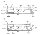
電気回路において一定の周波数信号を得るため、圧電発振器が広く利用されている。特許文献1には、図9に示す従来の圧電発振器501が記載されている。なお、図9(1)は製造途中における平面図であり、図9(2)は図9(1)のH−H線に相当する部分における側面断面図である。図9(2)に示す圧電発振器501では、リードフレーム530の下面に圧電振動子510が実装され、リードフレーム530の上面に集積回路素子(IC)560が実装され、全体を樹脂封止するように樹脂パッケージ570が形成されている。なお、図9に示すシリンダ型の圧電振動子510は、圧電平板に励振電極を形成した圧電振動片を、金属製のシリンダ内部に封止して、前記励振電極と導通する外部リード524をシリンダ外部に引き出したものである。一方、IC560は発振回路を形成したものである。
Piezoelectric oscillators are widely used to obtain a constant frequency signal in an electric circuit.
図9(1)は、樹脂パッケージ570を形成する直前の状態を示している。リードフレーム530の中央にはダイパッド552が配置され、その上にIC560が実装されている。また、ダイパッド552の四方には圧電発振器501の実装用リード542が配置され、それぞれがIC560とワイヤボンディングにより電気的に接続されている。なお、実装用リード542のアウター部分は、樹脂パッケージ570の形成後に下方に折り曲げられて、実装端子が形成される。さらに、図9(1)の上下方向における実装用リード542の中間部には、圧電振動子510とIC560との接続用リード532が形成されている。そして、接続用リード532の下面には圧電振動子510の外部リード524が接続され、接続用リード532の上面はIC560とワイヤボンディングにより接続されている。これにより、圧電振動子510とIC560とが電気的に接続される。
なお特許文献2にも同様の構成が示されている。
圧電発振器は携帯電話等の通信手段に使用されるが、携帯電話等に対する小型化の要請は強くなっている。これに伴って、圧電発振器にも小型化、薄型化が強く要求されている。なお近時では、圧電振動片をパッケージ内部に封止するとともに、圧電振動片の励振電極と導通する外部電極をパッケージの裏面上に形成した、パッケージ型(平面実装型)の圧電振動子が開発されている。図9に示すシリンダ型の圧電振動子510に代わって、パッケージ型の圧電振動子が開発されたのも、圧電発振器の小型化、薄型化の要求に応えるためである。
Piezoelectric oscillators are used for communication means such as mobile phones, but there is an increasing demand for miniaturization of mobile phones and the like. Along with this, there is a strong demand for miniaturization and thinning of piezoelectric oscillators. Recently, a package type (planar mounting type) piezoelectric vibrator has been developed in which the piezoelectric vibrating piece is sealed inside the package and an external electrode that is electrically connected to the excitation electrode of the piezoelectric vibrating piece is formed on the back surface of the package. Has been. The package-type piezoelectric vibrator was developed in place of the cylinder-type
ところで、圧電発振器は、小型化されるのに伴って、実装基板に接合する実装端子なども小型化される。したがって、圧電発振器は、小型化されればされるほど、実装端子の実装基板への接合面積が小さくなって接合強度が低下する。このため、圧電発振器は、携帯電話等の携帯用電子機器に搭載された場合、これらが取り落とされると、大きな衝撃力が作用して実装基板との接合部において剥離する可能性が増大する。このことは、樹脂パッケージを構成している樹脂とリードフレームの端子との接合部においても同様である。そこで、圧電発振器は、小型化されればされるほど、実装基板や、樹脂パッケージを構成する樹脂との接合強度を向上させることが大きな課題となる。 By the way, as the piezoelectric oscillator is reduced in size, the mounting terminals to be bonded to the mounting substrate are also reduced in size. Therefore, the smaller the piezoelectric oscillator is, the smaller the bonding area of the mounting terminal to the mounting substrate and the lower the bonding strength. For this reason, when the piezoelectric oscillator is mounted on a portable electronic device such as a mobile phone, if the piezoelectric oscillator is removed, a possibility that a large impact force acts and the piezoelectric oscillator is peeled off at the joint portion with the mounting substrate increases. This also applies to the joint portion between the resin constituting the resin package and the lead frame terminal. Therefore, as the size of the piezoelectric oscillator is reduced, it becomes a big problem to improve the bonding strength between the mounting substrate and the resin constituting the resin package.
ところが、上述した圧電発振器では、接続用リードを実装用リードの中間部に配置する必要があるため、平面サイズが大きくなるという問題がある。そのため、圧電発振器の小型化には限界がある。
そこで本発明は、平面サイズを小さくすることにより小型化を可能にすることを目的とする。
また、本発明は、接合強度を向上させることを目的としている。
さらに、本発明は、実装強度を向上させることを目的としている。
However, in the above-described piezoelectric oscillator, there is a problem that the plane size is increased because the connecting lead needs to be arranged in the middle part of the mounting lead. Therefore, there is a limit to downsizing the piezoelectric oscillator.
Accordingly, an object of the present invention is to enable miniaturization by reducing the planar size.
Another object of the present invention is to improve the bonding strength.
A further object of the present invention is to improve the mounting strength.
上記の目的を達成するために、本発明に係る圧電発振器は、複数枚のリードフレームに形成された複数のリードを有する圧電発振器であって、前記複数のリードに形成され相互に離間した端子が、パッケージの上下方向に複数段に配置されていることを特徴としている。このようになっている本発明は、端子をパッケージの上下方向に複数段に配置したことにより、端子を平面的に配列する必要がなく、平面サイズを小さくすることができ、小型化が可能となる。 In order to achieve the above object, a piezoelectric oscillator according to the present invention is a piezoelectric oscillator having a plurality of leads formed on a plurality of lead frames, and terminals formed on the plurality of leads and spaced apart from each other. It is characterized by being arranged in a plurality of stages in the vertical direction of the package. In the present invention thus configured, since the terminals are arranged in a plurality of stages in the vertical direction of the package, it is not necessary to arrange the terminals in a plane, the plane size can be reduced, and the size can be reduced. Become.
また、前記端子として少なくとも圧電振動子との接続用の接続端子と、実装基板への実装用の実装端子とを有し、前記接続端子と前記実装端子とが平面視において重なるように配置され、振動子パッケージの内部に圧電振動片を封止した前記圧電振動子を、前記接続端子に実装し、発振回路を形成したICを、前記リードフレームに実装し、前記実装端子の主面を外部に露出させつつ、前記リードフレームおよび前記圧電振動子を内部に封止して形成してもよい。この場合、圧電振動子をリードフレームに実装する前に、圧電振動子の周波数調整およびICの動作チェックを行なうことにより、良品の圧電振動子および良品のICを組み合わせて圧電発振器を形成することができる。これにより、良品のICを廃棄することがなくなってICの歩留まりが向上し、製造コストを削減することができる。 Further, the terminal has at least a connection terminal for connection with a piezoelectric vibrator and a mounting terminal for mounting on a mounting substrate, and the connection terminal and the mounting terminal are arranged so as to overlap in a plan view, The piezoelectric vibrator in which a piezoelectric vibrating piece is sealed inside a vibrator package is mounted on the connection terminal, an IC on which an oscillation circuit is formed is mounted on the lead frame, and the main surface of the mounting terminal is exposed to the outside. The lead frame and the piezoelectric vibrator may be sealed inside while being exposed. In this case, before mounting the piezoelectric vibrator on the lead frame, by adjusting the frequency of the piezoelectric vibrator and checking the operation of the IC, a piezoelectric oscillator can be formed by combining a good piezoelectric vibrator and a good IC. it can. As a result, non-defective ICs are not discarded, IC yield is improved, and manufacturing costs can be reduced.
さらに、リードフレームおよび圧電振動子の全体を樹脂封止する構成としたので、圧電振動子およびICの種類の組合せが変わっても、同じ樹脂成型モールドを使用することが可能である。したがって、多品種少量生産に対応することができる。また、リードフレームおよび圧電振動子の全体を絶縁することが可能となり、またゴミや水分の侵入を防止することが可能となる。したがって、電気的および化学的な故障の発生を防止することができる。 Furthermore, since the entire lead frame and the piezoelectric vibrator are sealed with resin, the same resin molding mold can be used even if the combination of the types of the piezoelectric vibrator and the IC changes. Therefore, it is possible to cope with a large variety and small quantity production. In addition, it is possible to insulate the entire lead frame and the piezoelectric vibrator, and to prevent entry of dust and moisture. Therefore, the occurrence of electrical and chemical failures can be prevented.
また、本発明は、圧電振動片と、該圧電振動片を封止したパッケージと、該パッケージの裏面に形成され、前記圧電振動片と電気的に接続された外部電極と、を有する圧電振動子と、発振回路が形成されたICと、上側リードフレームと下側リードフレームとで構成され、前記ICが実装された積層リードフレームと、を有し、前記上側リードフレームは、端部に位置する第1のパッドと、該第1のパッドより外側に位置する第1の傾斜部と、該第1の傾斜部より外側に位置する接続端子と、を備え、前記接続端子の主面に前記圧電振動子の前記外部電極が接続されて、前記積層リードフレームに前記圧電振動子が実装され、前記第1のパッドから前記傾斜部を上側に立ち上げて、前記上側リードフレームから離して平行に前記接続端子を配置し、前記第1のパッドを前記ICと接続し、前記下側リードフレームは、端部に位置する第2のパッドと、該第2のパッドより外側に位置する第2の傾斜部と、該第2の傾斜部より外側に位置する実装端子と、を備え、前記第2のパッドから前記傾斜部を下側に立ち上げて、前記下側リードフレームから離して平行に前記実装端子を配置し、前記第2のパッドを前記ICに接続し、前記実装端子の主面を外部に露出させつつ、前記積層リードフレームおよび前記圧電振動子を樹脂パッケージの内部に封止して形成した。 The present invention also provides a piezoelectric vibrator having a piezoelectric vibrating piece, a package in which the piezoelectric vibrating piece is sealed, and an external electrode formed on the back surface of the package and electrically connected to the piezoelectric vibrating piece. And an IC having an oscillation circuit formed thereon, an upper lead frame and a lower lead frame, and a laminated lead frame on which the IC is mounted. The upper lead frame is located at an end. A first pad; a first inclined portion positioned outside the first pad; and a connection terminal positioned outside the first inclined portion, wherein the piezoelectric element is disposed on a main surface of the connection terminal. The external electrode of the vibrator is connected, the piezoelectric vibrator is mounted on the laminated lead frame, the inclined portion is raised upward from the first pad, and separated from the upper lead frame in parallel with the Arrange the connection terminals The first pad is connected to the IC, and the lower lead frame includes a second pad located at an end, a second inclined portion located outside the second pad, A mounting terminal located outside the second inclined portion, and the inclined portion is raised from the second pad, and the mounting terminal is arranged in parallel away from the lower lead frame. The second lead pad is connected to the IC, and the laminated lead frame and the piezoelectric vibrator are sealed inside the resin package while the main surface of the mounting terminal is exposed to the outside.
この場合、接続端子および実装端子を重ねて配置することが可能となり、両者を並べて配置する必要がない。したがって、圧電発振器の平面サイズを小さくすることができる。なお、圧電振動子を積層リードフレームに実装する前に、圧電振動子の周波数調整およびICの動作チェックを行なうことにより、良品の圧電振動子および良品のICを組み合わせて圧電発振器を形成することができる。これにより、良品のICを廃棄することがなくなってICの歩留まりが向上し、製造コストを削減することができる。 In this case, the connection terminals and the mounting terminals can be arranged in an overlapping manner, and there is no need to arrange them both side by side. Therefore, the planar size of the piezoelectric oscillator can be reduced. Before mounting the piezoelectric vibrator on the laminated lead frame, a piezoelectric oscillator can be formed by combining a good piezoelectric vibrator and a good IC by adjusting the frequency of the piezoelectric vibrator and checking the operation of the IC. it can. As a result, non-defective ICs are not discarded, IC yield is improved, and manufacturing costs can be reduced.
さらに、積層リードフレームおよび圧電振動子の全体を樹脂封止する構成としたので、圧電振動子およびICの種類の組み合わせが変わっても、同じ樹脂成型モールドを使用することが可能である。したがって、多品種少量生産に対応することができる。また、積層リードフレームおよび圧電振動子の全体を絶縁することが可能となり、またゴミや水分の浸入を防止することが可能となる。したがって、電気的および化学的な故障の発生を防止することができる。 Furthermore, since the entire laminated lead frame and the piezoelectric vibrator are configured to be resin-sealed, the same resin molding mold can be used even if the combination of the types of the piezoelectric vibrator and the IC is changed. Therefore, it is possible to cope with a large variety and small quantity production. In addition, it is possible to insulate the laminated lead frame and the piezoelectric vibrator as a whole, and to prevent entry of dust and moisture. Therefore, the occurrence of electrical and chemical failures can be prevented.
また、本発明は、圧電振動片と、該圧電振動片を封止したパッケージと、該パッケージの裏面に形成され、前記圧電振動片と電気的に接続された外部電極と、を有する圧電振動子と、発振回路が形成されたICと、上側リードフレームと下側リードフレームとで構成され、前記ICが実装された積層リードフレームと、を有し、前記上側リードフレームは、端部に位置する第1のパッドと、該第1のパッドより外側に位置する第1の傾斜部と、該第1の傾斜部より外側に位置する接続端子と、を備え、前記接続端子の主面に前記圧電振動子の前記外部電極が接続されて、前記積層リードフレームに前記圧電振動子が実装され、前記第1のパッドから前記傾斜部を上側に立ち上げて、前記上側リードフレームから離して平行に前記接続端子を配置し、前記第1のパッドを前記ICと接続し、前記下側リードフレームは、端部に位置する第2のパッドと、該第2のパッドより外側に位置する実装端子を備え、前記第2のパッドと前記実装端子を互いに同一平面内に配置し、前記第2のパッドを前記ICに接続し、前記実装端子の主面を外部に露出させつつ、前記積層リードフレームおよび前記圧電振動子を樹脂パッケージの内部に封止して形成したことを特徴としている。
この場合において、前記上側リードフレームの前記第1のパッドと前記ICとは、ワイヤによって接続されており、前記第1の傾斜部は、ボンディングされた前記ワイヤの最大高さよりも大きく立ち上げて形成してあることを特徴としている。
本発明は、圧電振動片と、該圧電振動片を封止したパッケージと、該パッケージの裏面に形成され、前記圧電振動片と電気的に接続された外部電極と、を有する圧電振動子と、発振回路が形成されたICと、上側リードフレームと下側リードフレームとで構成され、前記ICが実装された積層リードフレームと、を有し、前記上側リードフレームは、端部に位置する第1のパッドと、該第1のパッドより外側に位置する接続端子を備え、前記接続端子の主面に前記圧電振動子の前記外部電極が接続されて、前記積層リードフレームに前記圧電振動子が実装され、前記第1のパッドと前記接続端子を互いに同一平面内に配置し、前記第1のパッドを前記ICと接続し、前記下側リードフレームは、端部に位置する第2のパッドと、該第2のパッドより外側に位置する第2の傾斜部と、該第2の傾斜部より外側に位置する実装端子と、を備え、前記第2のパッドから前記傾斜部を下側に立ち上げて、前記下側リードフレームから離して平行に前記実装端子を配置し、前記第2のパッドを前記ICに接続し、前記実装端子の主面を外部に露出させつつ、前記積層リードフレームおよび前記圧電振動子を樹脂パッケージの内部に封止して形成したことを特徴としている。
この場合において、前記下側リードフレームの前記第2のパッドと前記ICとは、ワイヤによって接続されており、前記第2の傾斜部は、ボンディングされた前記ワイヤの最大高さよりも大きく立ち上げて形成してあることを特徴としている。
The present invention also provides a piezoelectric vibrator having a piezoelectric vibrating piece, a package in which the piezoelectric vibrating piece is sealed, and an external electrode formed on the back surface of the package and electrically connected to the piezoelectric vibrating piece. And an IC having an oscillation circuit formed thereon, an upper lead frame and a lower lead frame, and a laminated lead frame on which the IC is mounted. The upper lead frame is located at an end. A first pad; a first inclined portion positioned outside the first pad; and a connection terminal positioned outside the first inclined portion, wherein the piezoelectric element is disposed on a main surface of the connection terminal. The external electrode of the vibrator is connected, the piezoelectric vibrator is mounted on the laminated lead frame, the inclined portion is raised upward from the first pad, and separated from the upper lead frame in parallel with the Arrange the connection terminals The first pad is connected to the IC, and the lower lead frame includes a second pad located at an end portion and a mounting terminal located outside the second pad, And the mounting terminal are arranged in the same plane, the second pad is connected to the IC, the main surface of the mounting terminal is exposed to the outside, and the laminated lead frame and the piezoelectric vibrator are It is characterized by being sealed inside the resin package.
In this case, the first pad of the upper lead frame and the IC are connected by a wire, and the first inclined portion is formed to rise higher than the maximum height of the bonded wire. It is characterized by being.
The present invention provides a piezoelectric vibrator having a piezoelectric vibrating piece, a package in which the piezoelectric vibrating piece is sealed, and an external electrode formed on the back surface of the package and electrically connected to the piezoelectric vibrating piece. An IC including an oscillation circuit, an upper lead frame and a lower lead frame, and a laminated lead frame on which the IC is mounted. The upper lead frame is located at an end. And a connection terminal located outside the first pad, the external electrode of the piezoelectric vibrator is connected to the main surface of the connection terminal, and the piezoelectric vibrator is mounted on the laminated lead frame The first pad and the connection terminal are arranged in the same plane, the first pad is connected to the IC, and the lower lead frame has a second pad located at an end; The second pack A second inclined portion located on the outer side, and a mounting terminal located on the outer side of the second inclined portion, wherein the inclined portion is raised downward from the second pad, and the lower side The mounting terminals are arranged in parallel away from the lead frame, the second pad is connected to the IC, and the main surface of the mounting terminals is exposed to the outside, and the laminated lead frame and the piezoelectric vibrator are made of resin. It is characterized by being sealed inside the package.
In this case, the second pad of the lower lead frame and the IC are connected by a wire, and the second inclined portion rises larger than the maximum height of the bonded wire. It is characterized by being formed.
このようになっている本発明は、前記と同様の効果が得られるとともに、積層リードフレームが一方のリードフレームのみを折曲して形成されるため、高さ寸法を小さくすることができ、圧電発振器をより薄型にすることができる。また、他方のリードフレームを折曲加工する必要がないため、工程の簡素化が図れる。 According to the present invention thus configured, the same effect as described above can be obtained, and since the laminated lead frame is formed by bending only one lead frame, the height dimension can be reduced, and the piezoelectric structure can be reduced. The oscillator can be made thinner. Further, since it is not necessary to bend the other lead frame, the process can be simplified.
また、前記積層リードフレームに、前記ICの特性検査、特性調整および/または前記圧電振動子と前記接続端子との導通確認をするための調整端子を形成し、前記調整端子を外部に露出させつつ、前記積層リードフレームおよび前記圧電振動子を樹脂パッケージの内部に封止して形成してもよい。これにより、樹脂封止後の製品状態において、ICの特性検査、特性調整および/または圧電振動子と接続端子との導通確認を行なうことができる。 The laminated lead frame is formed with an adjustment terminal for inspecting the characteristics of the IC, adjusting the characteristics and / or confirming the continuity between the piezoelectric vibrator and the connection terminal, and exposing the adjustment terminal to the outside. The laminated lead frame and the piezoelectric vibrator may be sealed inside a resin package. Thereby, in the product state after resin sealing, it is possible to perform IC characteristic inspection, characteristic adjustment, and / or conduction confirmation between the piezoelectric vibrator and the connection terminal.
そして、前記実装端子の主面に加えて、前記実装端子の側面を外部に露出させつつ、前記積層リードフレームおよび前記圧電振動子を樹脂パッケージの内部に封止して形成してよい。この場合、実装端子の主面からはみ出したはんだが、実装端子の側面に沿ってせり上がる。その結果、実装基板の電極から実装端子の側面にかけてフィレットが形成される。これにより、実装基板の電極と圧電発振器の実装端子との接続を、外観から簡単に確認することができる。 Then, in addition to the main surface of the mounting terminal, the laminated lead frame and the piezoelectric vibrator may be sealed inside the resin package while exposing the side surface of the mounting terminal to the outside. In this case, the solder protruding from the main surface of the mounting terminal rises along the side surface of the mounting terminal. As a result, a fillet is formed from the electrode of the mounting substrate to the side surface of the mounting terminal. Thereby, the connection between the electrode of the mounting substrate and the mounting terminal of the piezoelectric oscillator can be easily confirmed from the appearance.
また、前記実装端子は、端部が前記樹脂パッケージの側面から突出させて形成してもよい。これにより、実装端子を実装基板に接合したときに、はんだが実装端子の樹脂パッケージから突出した部分にせり上がってフィレットを形成するため、目視によって実装(接合)の良否を容易に判断することができる。また、はんだが樹脂パッケージから突出している実装端子を覆うため、実装強度を向上することができる。 Further, the mounting terminal may be formed with an end portion protruding from a side surface of the resin package. As a result, when the mounting terminal is joined to the mounting substrate, the solder rises to a portion protruding from the resin package of the mounting terminal to form a fillet, so it is possible to easily determine whether the mounting (joining) is good or not visually. it can. Further, since the solder covers the mounting terminals protruding from the resin package, the mounting strength can be improved.
前記下側リードフレームは、前記樹脂パッケージの樹脂を入り込ませる切り欠きが形成されている。圧電発振器の小型化が進展すると、実装用リードにアンカー効果が得られる樹脂との引っ掛かり部を形成することが困難となる。そこで、実装用リードを凸部や切り欠き、凸部など有する異形に形成することにより、樹脂と引っ掛かって大きなアンカー効果が得られ、実装強度を向上させることができる。 The lower lead frame is formed with a notch for allowing the resin of the resin package to enter. As miniaturization of the piezoelectric oscillator progresses, it becomes difficult to form a catching portion with a resin capable of obtaining an anchor effect on the mounting lead. Therefore, by forming the mounting lead into an irregular shape having a convex portion, a notch, a convex portion, or the like, a large anchor effect can be obtained by being caught by the resin, and the mounting strength can be improved.
前記上側リードフレームは、前記樹脂パッケージの樹脂を入り込ませる切り欠きが形成されている。これにより、圧電発振器がより小型化された場合であっても、樹脂に対するアンカー効果を大きくすることが可能となり、接合強度を向上することができる。 The upper lead frame is formed with a notch for allowing the resin of the resin package to enter. As a result, even when the piezoelectric oscillator is further downsized, the anchor effect on the resin can be increased, and the bonding strength can be improved.
前記ICは、前記積層リードフレームのいずれか一方に実装することができる。これにより、仮に圧電発振器の下方から水分が侵入してもICまで到達しにくくなるので、ICの故障を防止することができる。また、ICに温度補償回路を付加した場合には、その温度センサが圧電振動子の近くに配置されるので、温度センサと圧電振動片との温度差を小さくすることができる。したがって、圧電振動片の温度特性を正確に補正することができる。 The IC can be mounted on any one of the laminated lead frames. Accordingly, even if moisture enters from below the piezoelectric oscillator, it becomes difficult to reach the IC, so that it is possible to prevent IC failure. Further, when a temperature compensation circuit is added to the IC, the temperature sensor is disposed near the piezoelectric vibrator, so that the temperature difference between the temperature sensor and the piezoelectric vibrating piece can be reduced. Therefore, the temperature characteristics of the piezoelectric vibrating piece can be accurately corrected.
前記圧電振動子の高さ方向に対する係止部を前記パッケージの側面に形成した上で、前記積層リードフレームおよび前記圧電振動子を樹脂パッケージの内部に封止してもよい。これにより、圧電振動子が圧電発振器から抜けにくくなるため強固に固定されることとなる。 A latching portion for the height direction of the piezoelectric vibrator may be formed on a side surface of the package, and the laminated lead frame and the piezoelectric vibrator may be sealed inside a resin package. As a result, the piezoelectric vibrator is hard to be detached from the piezoelectric oscillator, and is firmly fixed.
前記圧電振動子のリッドの上面を外部に露出させつつ、前記積層リードフレームおよび前記圧電振動子を樹脂パッケージの内部に封止して形成してもよい。リッドの上面には圧電振動子の製品仕様が記載されているので、リッドを露出させることにより、樹脂パッケージの表面に製品仕様を記載する必要がなくなる。また、樹脂成型モールド金型内においてリッドの位置が固定されるため、圧電振動子の姿勢を安定させることができる。そして、前記圧電振動子のリッドを前記樹脂パッケージの内部に封止して形成してもよい。これにより、実装端子の表面にはんだメッキを施す工程において、露出したリッドがはんだメッキで被覆されるのを防止するため、リッドの上面をマスクする必要がなくなる。 The laminated lead frame and the piezoelectric vibrator may be sealed inside the resin package while the upper surface of the lid of the piezoelectric vibrator is exposed to the outside. Since the product specifications of the piezoelectric vibrator are described on the upper surface of the lid, it is not necessary to describe the product specifications on the surface of the resin package by exposing the lid. In addition, since the position of the lid is fixed in the resin molding mold, the posture of the piezoelectric vibrator can be stabilized. Then, the lid of the piezoelectric vibrator may be sealed inside the resin package. This eliminates the need to mask the upper surface of the lid in order to prevent the exposed lid from being covered with the solder plating in the step of performing solder plating on the surface of the mounting terminal.
一方、本発明に係る圧電発振器の製造方法は、2枚のリードフレームを上下に重ね合わせて構成される積層リードフレームにつき、上側リードフレームは、端部に位置する第1のパッドと、該第1のパッドより外側に位置する第1の傾斜部と、該第1の傾斜部より外側に位置する接続端子と、を形成し、前記接続端子の主面に前記圧電振動子の前記外部電極が接続されて、前記積層リードフレームに前記圧電振動子が実装され、前記第1のパッドから前記傾斜部を上側に立ち上げて、前記上側リードフレームから離して平行に前記接続端子を配置するとともに、前記下側リードフレームは、端部に位置する第2のパッドと、該第2のパッドより外側に位置する第2の傾斜部と、該第2の傾斜部より外側に位置する実装端子と、を形成し、前記第2のパッドから前記傾斜部を下側に立ち上げて、前記下側リードフレームから離して平行に前記実装端子を配置し、前記各リードフレームを積層して前記積層リードフレームを形成する工程と、発振回路を形成したICを、前記積層リードフレームに実装する工程と、パッケージの内部に圧電振動片を封止した前記圧電振動子を、前記積層リードフレームに実装する工程と、前記実装端子の主面を外部に露出させつつ、前記積層リードフレームおよび前記圧電振動子を樹脂パッケージの内部に封止する工程と、を有する構成とした。これにより圧電振動器の平面サイズを小さくすることができる。 On the other hand, in the method for manufacturing a piezoelectric oscillator according to the present invention, the upper lead frame includes a first pad located at an end, and the first lead frame. A first inclined portion located outside the one pad and a connection terminal located outside the first inclined portion, and the external electrode of the piezoelectric vibrator is formed on a main surface of the connection terminal. The piezoelectric vibrator is mounted on the laminated lead frame, the inclined portion is raised upward from the first pad, and the connection terminals are arranged in parallel away from the upper lead frame, The lower lead frame includes a second pad positioned at an end, a second inclined portion positioned outside the second pad, and a mounting terminal positioned outside the second inclined portion; Forming the said A step of raising the inclined portion downward from the two pads, disposing the mounting terminals in parallel away from the lower lead frame, and laminating the lead frames to form the laminated lead frame; Mounting the IC on which the oscillation circuit is formed on the multilayer lead frame, mounting the piezoelectric vibrator having a piezoelectric vibrating piece sealed inside the package on the multilayer lead frame, and main terminals of the mounting terminals And a step of sealing the laminated lead frame and the piezoelectric vibrator inside the resin package while exposing the surface to the outside. Thereby, the planar size of the piezoelectric vibrator can be reduced.
さらに、本発明に係る圧電発振器の製造方法は、2枚のリードフレームを上下に重ね合わせて構成される積層リードフレームにつき、上側リードフレームは、端部に位置する第1のパッドと、該第1のパッドより外側に位置する第1の傾斜部と、該第1の傾斜部より外側に位置する接続端子と、を形成し、前記接続端子の主面に前記圧電振動子の前記外部電極が接続されて、前記積層リードフレームに前記圧電振動子が実装され、前記第1のパッドから前記傾斜部を上側に立ち上げて、前記上側リードフレームから離して平行に前記接続端子を配置するとともに、前記下側リードフレームは、端部に位置する第2のパッドと、該第2のパッドより外側に位置する実装端子を形成し、前記第2のパッドと前記実装端子を互いに同一平面内に配置し、前記各リードフレームを積層して前記積層リードフレームを形成する工程と、発振回路を形成したICを、前記積層リードフレームに実装する工程と、パッケージの内部に圧電振動片を封止した前記圧電振動子を、前記積層リードフレームに実装する工程と、前記実装端子の主面を外部に露出させつつ、前記積層リードフレームおよび前記圧電振動子を樹脂パッケージの内部に封止する工程と、を有することを特徴としている。これにより、実装用リードは、傾斜部が形成されないため、実装端子の実質的な接合面積を大きくすることができ、実装基板に対する接合強度を大きくすることができる。実装用リードの基端側の薄肉化は、プレスによる塑性加工やエッチングによって容易に行なうことができる。 Furthermore, in the method for manufacturing a piezoelectric oscillator according to the present invention, the upper lead frame includes a first pad located at an end of the laminated lead frame formed by superimposing two lead frames on the upper and lower sides, and the first lead frame. A first inclined portion located outside the one pad and a connection terminal located outside the first inclined portion, and the external electrode of the piezoelectric vibrator is formed on a main surface of the connection terminal. The piezoelectric vibrator is mounted on the laminated lead frame, the inclined portion is raised upward from the first pad, and the connection terminals are arranged in parallel away from the upper lead frame, The lower lead frame forms a second pad located at an end portion and a mounting terminal located outside the second pad, and the second pad and the mounting terminal are arranged in the same plane. A step of laminating the lead frames to form the laminated lead frame; a step of mounting an IC in which an oscillation circuit is formed on the laminated lead frame; and the piezoelectric having a piezoelectric vibrating piece sealed in a package Mounting the vibrator on the multilayer lead frame, and sealing the multilayer lead frame and the piezoelectric vibrator inside a resin package while exposing a main surface of the mounting terminal to the outside. It is characterized by that. Thereby, since the inclined part is not formed in the mounting lead, the substantial bonding area of the mounting terminal can be increased, and the bonding strength to the mounting substrate can be increased. Thinning of the base end side of the mounting lead can be easily performed by plastic working or etching using a press.
また、前記実装端子の主面に付着した樹脂を除去する工程を有する構成としてもよい。これにより、実装端子の主面にはんだメッキを施すことができる。さらに、前記樹脂パッケージの内部に封止する工程は、前記実装端子の主面を金型面に押圧して行ない、その後の前記樹脂パッケージを前記リードフレームの枠部から切り離す工程において、前記実装端子の不要部を切断することができる。これにより、樹脂封止の際に実装端子の主面が金型面に密着させられるため、実装端子の主面に樹脂が付着するのを防止でき、主面に付着した樹脂を除去する工程を省くことができる。そして、樹脂パッケージをリードフレームの枠部から切り離すときに、実装端子の不要部を切断して除去すれば、実装面積が大きくなるのを防ぐことができる。 Moreover, it is good also as a structure which has the process of removing the resin adhering to the main surface of the said mounting terminal. Thereby, solder plating can be performed on the main surface of the mounting terminal. Further, the step of sealing the inside of the resin package is performed by pressing the main surface of the mounting terminal against the mold surface, and the step of separating the resin package from the frame portion of the lead frame in the subsequent step. Unnecessary parts can be cut. As a result, since the main surface of the mounting terminal is brought into close contact with the mold surface during resin sealing, it is possible to prevent the resin from adhering to the main surface of the mounting terminal and to remove the resin adhering to the main surface. It can be omitted. Then, when the resin package is separated from the frame portion of the lead frame, if the unnecessary portion of the mounting terminal is cut and removed, an increase in the mounting area can be prevented.
そして、本発明に係る電子機器は、上記いずれかの圧電発振器を有することを特徴としている。これにより、電子機器の小型化が可能になるとともに、耐衝撃性に優れ、信頼性の高い電子機器を得ることができる。 And the electronic device which concerns on this invention has one of the said piezoelectric oscillators, It is characterized by the above-mentioned. Accordingly, it is possible to reduce the size of the electronic device, and it is possible to obtain a highly reliable electronic device having excellent impact resistance.
本発明に係る圧電発振器およびその製造方法並びに電子機器の好ましい実施の形態を、添付図面に従って詳細に説明する。なお以下に記載するのは本発明の実施形態の一態様にすぎず、本発明はこれらに限定されるものではない。 DESCRIPTION OF EMBODIMENTS Preferred embodiments of a piezoelectric oscillator, a manufacturing method thereof, and an electronic device according to the present invention will be described in detail with reference to the accompanying drawings. Note that what is described below is only one aspect of the embodiment of the present invention, and the present invention is not limited thereto.
最初に、第1実施形態について説明する。
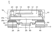
図1に、第1実施形態に係る圧電発振器を分解した状態の斜視図を示す。また図2に、図1のA−A線における側面断面図を示す。なお、図2では樹脂パッケージ70を取り除いた状態を示している。すなわち、図2における積層リードフレーム50の部分の断面は、実際には切断されていない位置の端子部分を付しているが、これは理解の便宜のために付したもので、切断面を示すものではなく、各端子部分等の上下方向(垂直方向)の位置を示すものである。第1実施形態に係る圧電発振器1は、2枚のリードフレーム30、40で構成される積層リードフレーム50につき、圧電振動子10との接続用リード32を上側リードフレーム30に形成し、その接続用リード32を上側に立ち上げて接続端子36を形成するとともに、実装基板への実装用リード42を下側リードフレーム40に形成し、その実装用リード42を下側に立ち上げて実装端子46を形成し、発振回路を形成したIC60を積層リードフレーム50に実装し、パッケージ20の内部に圧電振動片12を封止した圧電振動子10を積層リードフレーム50に実装し、前記実装端子46の主面を露出させつつ、積層リードフレーム50および圧電振動子10を樹脂パッケージ70(図2参照)の内部に封止して形成したものである。なおICは、抵抗やコンデンサ等の電子部品であってもよい。
First, the first embodiment will be described.
FIG. 1 is a perspective view showing a state where the piezoelectric oscillator according to the first embodiment is disassembled. FIG. 2 is a side sectional view taken along line AA in FIG. FIG. 2 shows a state where the
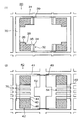
図3にリードフレームの平面図を示す。なお、図3(1)は上側リードフレームの平面図であり、図3(2)は下側リードフレームの平面図である。第1実施形態では、2枚のリードフレーム30、40を重ね合わせて積層リードフレーム50を形成する。各リードフレーム30、40は、導電性を有する金属シートに井桁状の枠部31、41を設けるとともに、各枠部31、41の内側に同一のパターンを繰り返し形成したものである。
FIG. 3 shows a plan view of the lead frame. 3A is a plan view of the upper lead frame, and FIG. 3B is a plan view of the lower lead frame. In the first embodiment, the
図3(1)に示す一方側のリードフレームである上側リードフレーム30では、枠部31の内側の四隅に、圧電振動子との接続用リード32を形成する。なお圧電振動子には、一対の励振電極と導通する外部電極およびGND用の外部電極を合わせて、少なくとも3個の外部電極が形成されるので、上側リードフレーム30には少なくとも3個の接続用リード32を形成する。そして、枠部31の長辺方向における各接続用リード32の内側端部には、ワイヤボンディング用のパッド34を形成する。なお、パッド34を枠部31と同一平面上に支持すべく、パッド34を枠部31の長辺に接続する。これにより、接続用リード32が枠部31に固定される。一方、パッド34の外側に傾斜部35を形成し、さらに傾斜部35の外側に接続端子36を形成する。そして図1に示すように、パッド34から傾斜部35を上側に立ち上げることにより、上側リードフレーム30から所定距離をおいて平行に接続端子36を配置する。なお所定距離とは、IC60にボンディングされたワイヤ62の最大高さより大きい距離とする。
In the upper lead frame 30 that is one lead frame shown in FIG. 3A, lead 32 for connection with the piezoelectric vibrator is formed at the four corners inside the
図3(2)に示す他方側のリードフレームである下側リードフレーム40では、枠部41の内側の四隅に、実装基板への実装用リード42を形成する。なお、枠部41の短辺方向における各実装用リード42の内側端部には、ワイヤボンディング用のパッド44を形成する。なお、パッド44を枠部41と同一平面上に支持すべく、パッド44を枠部41の短辺に接続する。これにより、実装用リード42が枠部41に固定される。一方、パッド44の外側に傾斜部45を形成し、さらに傾斜部45の外側に実装端子46を形成する。そして図1に示すように、パッド44から傾斜部45を下側に立ち上げることにより、下側リードフレーム40から所定距離をおいて平行に実装端子46を配置する。
In the
また、枠部41の短辺方向における各実装用リード42の中間部には、ICの特性検査、特性調整および/または圧電振動子と接続端子との導通確認をするための調整端子54を形成する。なお、特性検査とは、樹脂成形後におけるICの動作チェックや、圧電発振器としての特性検査などをいう。また、特性調整とは、ICに温度補償回路が付加された場合に、圧電発振器の温度による周波数変化を補正したり、入力電圧によって周波数を変化させる機能がICに付加された場合に、その変化感度を調整したりすることなどをいう。調整端子54は、枠部41の短辺に接続して、下側リードフレーム40と同一平面上に支持する。なお、下側リードフレーム40から下側に所定距離をおいて実装端子46を配置するので、調整端子54が実装基板の電極等と短絡することはない。一方、下側リードフレーム40における枠部41内の中央部には、ダイパッド52を形成する。ダイパッド52は、枠部41の長辺に接続して、下側リードフレーム40と同一平面上に支持する。なお、調整端子54およびダイパッド52は、上側リードフレームに形成してもよい。また、接続端子、実装端子、調整端子およびダイパッドが各枠部に接続される位置は、長辺または短辺に限定されるものではない。例えば、調整端子数が多い場合には、調整端子は長辺側に接続され、ダイパッドは短辺側に接続される。
In addition, an
そして、上側リードフレーム30と下側リードフレーム40とを重ね合わせ、積層リードフレームを形成する。上側リードフレーム30および下側リードフレーム40は、それぞれの枠部31、41にスポット溶接等を施すことによって固着する。なお、枠部31、41の内側では、上側リードフレーム30および下側リードフレーム40が接触しないように、各リードフレームの各リードを形成する。これによって、積層リードフレーム50は、相互に離間した端子が上下方向に2段に形成される。すなわち、積層リードフレーム50は、接続端子36と実装端子46とが平面視において同じ位置に重なった状態で配置される。
Then, the upper lead frame 30 and the
一方、図1に示すように、ダイパッド52の上面に集積回路素子(IC)60を実装する。IC60には発振回路を形成し、必要に応じて温度補償回路や電圧制御回路を付加する。そして、接着剤を介してIC60をダイパッド52の上面に装着する。なお、IC60はダイパッド52の下面に装着してもよい。もっとも、ダイパッド52の上面にIC60を装着すれば、仮に圧電発振器の下方から水分が侵入してもIC60まで到達しにくくなるので、IC60の故障を防止することができる。また、IC60に温度補償回路を付加した場合には、その温度センサが圧電振動子10の近くに配置されるので、温度センサと圧電振動片12との温度差を小さくすることができる。したがって、圧電振動片12の温度特性を正確に補正することができる。
On the other hand, as shown in FIG. 1, an integrated circuit element (IC) 60 is mounted on the upper surface of the
さらに、積層リードフレーム50の各端子とIC60上面の各端子とを電気的に接続する。具体的には、接続端子36のパッド34、実装端子46のパッド44および調整端子54と、IC60上面の各端子とを、ワイヤボンディングにより接続する。なお、接続用リード32に切り欠き38を形成したので、実装端子46のパッド44が上方に露出する。これにより、実装端子46のパッド44に対してワイヤボンディングを行なうことができる。
Further, each terminal of the
一方で、圧電振動片12をパッケージ20の内部に封入した圧電振動子10を形成する。図2に示すように、パッケージ20は、セラミック材料等からなる複数のシートを積層・焼成して形成する。具体的には、各シートを所定の形状にブランクし、各シートの表面に所定の配線パターンを形成した上で、各シートを積層・焼成する。このパッケージ20にはキャビティ21を形成し、キャビティ21の底面にはマウント電極22を形成する。また、パッケージ20の裏面には外部電極24を形成し、配線パターン23および24aを介してマウント電極22との導通を確保する。なお、側面電極24aではなくスルーホールを介して上下接続してもよい。
On the other hand, the
圧電振動片12は、図1に示すように、水晶等の圧電材料からなる平板の両面に、励振電極14を形成したものである。なお、圧電平板の端部には、各励振電極14と導通する接続電極15を形成する。そして、図2に示すように、パッケージ20におけるキャビティ21の内部に、圧電振動片12を片持ち状態で実装する。具体的には、パッケージ20のマウント電極22に導電性接着剤13を塗布し、圧電振動片12の接続電極15(図1参照)を接着する。これにより、パッケージ20の外部電極24から圧電振動片12の励振電極14(図1参照)に対して通電可能となる。なお、圧電振動片12は両持ち実装であっても構わない。
As shown in FIG. 1, the piezoelectric vibrating
さらに、パッケージ20におけるキャビティ21の開口部にリッド28を装着して、キャビティ21の内部を窒素雰囲気や真空雰囲気に気密封止する。なお、金属製リッドの場合はシーム溶接により、ガラス製リッドの場合は低融点ガラスを介して、パッケージ20に装着する。以上により圧電振動子10が完成する。なお、パッケージ20の内部に実装するのは、ATカット圧電振動片に限られず、音叉型圧電振動片やSAWチップであってもよい。
Further, a
なお、圧電振動子10を積層リードフレーム50に実装する前に、圧電振動子10の周波数調整およびIC60の動作チェックを行なう。これにより、良品の圧電振動子10および良品のIC60を組み合わせて圧電発振器を形成することができる。なお、パッケージの内部にまずICを実装し、その上方に圧電振動片を実装するタイプの圧電発振器では、圧電振動片を実装した後の周波数調整段階で圧電振動片の不良が発見されることがある。この場合、不良品の圧電振動片とともに良品のICも廃棄することになる。この点、第1実施形態では、良品のICを廃棄することがなくなるので、ICの歩留まりが向上し、製造コストを削減することができる。
Before mounting the
そして、圧電振動子10を積層リードフレーム50に実装する。具体的には、はんだ25や導電性接着剤等を介して、圧電振動子10の外部電極24を積層リードフレームの接続端子に接続する。なお、圧電振動子10の外部電極24はパッケージ20の裏面のみに形成してもよいが、裏面から側面にかけて外部電極24aを延長形成するのが好ましい。この場合、パッケージ20の裏面からはみ出したはんだが、側面の外部電極24aに沿ってせり上がる。その結果、積層リードフレーム50の接続端子36からパッケージ側面の外部電極24aにかけてフィレット25aが形成される。これにより、積層リードフレーム50の接続端子36と圧電振動子10の外部電極24との接続を、外観から簡単に確認することができる。なお、圧電振動子10の外部電極24は、パッケージ20の側面のみに形成してもよい。また、本実施形態では圧電振動子を接続端子のみで支持しているが、電気的に独立したダミーの接続端子等を加えて圧電振動子を支持すれば、支持力の向上およびリードフレームの変形防止が可能となる。
Then, the
そして、積層リードフレーム50および圧電振動子10を樹脂パッケージ70の内部に封止する。具体的には、圧電振動子10を実装した積層リードフレーム50を樹脂成型モールド内に配置して、熱硬化性樹脂を射出成型することにより樹脂パッケージ70を形成する。樹脂パッケージ70は、図3に示すように、各リードフレーム30、40の枠部31、41の内側に形成する。樹脂パッケージ70の成型後には、各リードフレーム30、40の枠部31、41と各リードとの接続部を切断する。その切断位置39、49は、樹脂パッケージ70の表面付近とするのが好ましい。なお、ICの調整端子54は、樹脂パッケージ70から突出させて切断する。
Then, the
図2に示すように、積層リードフレーム50および圧電振動子10を樹脂パッケージ70の内部に封止することにより、両者の相対位置を固定することができる。なお、圧電振動子10のパッケージ20の側面に凹凸を形成して樹脂封止すれば、その凹凸が係止部となって、圧電振動子が圧電発振器から抜けにくくなるため強固に固定されることとなる。図4に、圧電振動子のパッケージの側面角部に形成されたキャスタレーションを示す。パッケージ20の側面には、一般にキャスタレーション18が形成される。そこで、キャスタレーション18に係止部19を形成する。係止部19を形成するには、パッケージ20を構成するセラミックシートの一部20bにつき、図4(1)ないし図4(8)のように、キャスタレーションとなる貫通孔の直径を変更したり、貫通孔の穿設位置を変更したりすればよい。なお、図4(1)ないし図4(3)はパッケージの角部におけるキャスタレーションに係止部を形成した例であり、図4(4)ないし図4(8)はパッケージの側面におけるキャスタレーションに係止部を形成した例である。
As shown in FIG. 2, by sealing the
一方、樹脂パッケージ70の上面には、圧電振動子10のリッド28の上面を露出させる。リッド28の上面には圧電振動子10の製品仕様が記載されているので、リッド28を露出させることにより、樹脂パッケージ70の表面に製品仕様を記載する必要がなくなる。また、樹脂成型モールド内における圧電振動子10の姿勢を安定させることができる。一方、後述するように、実装端子46の表面にはんだメッキを施す工程では、露出したリッド28がはんだメッキで被覆されるのを防止するため、リッド28の上面をマスクする必要がある。この点、樹脂パッケージ70の内部にリッド28を封止した場合には、かかる必要がない。
On the other hand, the upper surface of the
また、樹脂パッケージ70の下面には、実装端子46の主面を露出させる。図5(1)に図2のD矢視図を示し、図5(2)に図5(1)のF−F線における底面断面図を示す。図5(1)に示すように、本実施形態に係る圧電発振器1は、実装基板の電極8に対して、はんだ9を介して実装する。そこで、実装端子46は、その主面に加えて側面46aも露出させるのが好ましい。この場合、実装端子46の主面からはみ出したはんだ9が、側面46aに沿ってせり上がる。その結果、実装基板の電極8から実装端子の側面46aにかけてフィレット9aが形成される。これにより、実装基板の電極8と圧電発振器1の実装端子46との接続を、外観から簡単に確認することができる。
Further, the main surface of the mounting
また、図5(2)に示すように、実装端子46の主面にあらかじめディンプル(凹部)47を形成しておいてもよい。ディンプル47は、実装端子46の主面におけるディンプル47の形成部分以外の部分をマスクして、実装端子46の主面をハーフエッチングすることにより形成する。このような実装端子46を有する圧電発振器1を実装すると、ディンプル47にはんだが入り込んでアンカー効果を発揮する。したがって、圧電発振器1の実装端子46を実装基板の電極8に対して強固に固着することができ、圧電発振器1の実装強度を向上することができる。
Further, as shown in FIG. 5 (2), dimples (concave portions) 47 may be formed in advance on the main surface of the mounting
なお、図5(1)に示すように、樹脂パッケージ70の下面に実装端子46の主面を露出させるには、樹脂成型モールドの底面に実装端子46の主面を面接触させた状態で樹脂を射出成型する。ところが、樹脂の射出圧力により、実装端子46の主面と樹脂成型モールドとの間に樹脂が入り込んで、実装端子46の主面に樹脂が付着してしまう。次述するように、実装端子46の主面にははんだメッキを施すが、実装端子46の主面に樹脂が付着しているとはんだメッキが付着しなくなる。そこで、実装端子46の主面に付着した樹脂を除去する作業を行なう。樹脂の除去は、研磨剤入りの液体や水などを実装端子46に向かって吹き付ける方法によって行なう。なお、実装端子46に向かってレーザを照射する方法や、薬品を塗布する方法などによって樹脂を除去してもよい。
As shown in FIG. 5A, in order to expose the main surface of the mounting
次に、実装端子46の下面にはんだメッキを施す。その際、露出したリッド28(図2参照)の上面がはんだメッキで被覆されないように、リッド28の上面をマスクして行なう。
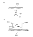
次に、圧電発振器の周波数調整を行なう。図6に、周波数調整工程の説明図を示す。なお図6は、図1のA−A線に相当する部分における側面断面図である。図6(1)に示すように、樹脂パッケージ70の外部に露出している調整端子54に下側からプローブ80を接触させ、IC60への書き込みを行なうことによって圧電発振器1の周波数調整を行なう。なお、プローブ80は、上側から接触させてもよい。なお、周波数調整後の調整端子54は、樹脂パッケージ70の表面付近で切り落とす。また、プローブ80により調整端子54を折り曲げつつ圧電発振器1の周波数調整を行ない、周波数調整後に調整端子54を切り落とすことなくそのまま製品化してもよい。図6(2)は、樹脂パッケージの変形例である。この変形例では、調整端子55の上方に樹脂パッケージ72を拡張成型している。この圧電発振器1の周波数調整も上記と同様に行なうが、周波数調整後に調整端子55を切り落とすことなく、そのまま製品化する。
Next, solder plating is applied to the lower surface of the mounting
Next, the frequency of the piezoelectric oscillator is adjusted. FIG. 6 is an explanatory diagram of the frequency adjustment process. FIG. 6 is a side sectional view of a portion corresponding to the line AA in FIG. As shown in FIG. 6 (1), the frequency of the
以上により、相互に離間した端子がパッケージの上下方向に複数段(実施形態の場合2段)に配置されている第1実施形態に係る圧電発振器1が完成する。
以上に詳述した第1実施形態にかかる圧電発振器により、平面サイズを小さくすることができる。
As described above, the
The plane size can be reduced by the piezoelectric oscillator according to the first embodiment described in detail above.
すなわち、第1実施形態では、2枚のリードフレームで構成される積層リードフレームにつき、圧電振動子との接続用リードを上側リードフレームに形成し、その接続用リードを上側に立ち上げて接続端子を形成するとともに、実装基板への実装用リードを下側リードフレームに形成し、その実装用リードを下側に立ち上げて実装端子を形成する構成とした。この場合、接続端子および実装端子を上下に重ねて配置することが可能となり、両者を並べて配置する必要がない。したがって、圧電発振器の平面サイズを小さくすることができる。また、実装端子の面積を広く確保することができる。 That is, in the first embodiment, for a laminated lead frame composed of two lead frames, a connection lead to the piezoelectric vibrator is formed on the upper lead frame, and the connection lead is raised upward to connect terminal In addition, a mounting lead to the mounting substrate is formed on the lower lead frame, and the mounting lead is raised downward to form a mounting terminal. In this case, it is possible to arrange the connection terminals and the mounting terminals so as to overlap each other, and it is not necessary to arrange both of them side by side. Therefore, the planar size of the piezoelectric oscillator can be reduced. In addition, a large area of the mounting terminal can be secured.
なお、第1実施形態では、圧電振動子および積層リードフレームの全体を樹脂パッケージの内部に封止する構成とした。この場合、圧電振動子およびICの種類の組み合わせが変わっても、同じ樹脂成型モールドを使用することが可能であり、多品種少量生産に対応することができる。また、樹脂パッケージの外形に対して接続端子の位置を正確に決めることができるので、圧電発振器を外形基準で位置決めすることにより、実装基板上に正確に実装することができる。さらに、樹脂封止することによって、圧電振動子および積層リードフレームの全体を絶縁することが可能となり、またゴミや水分の浸入を防止することが可能となる。したがって、電気的および化学的な故障の発生を防止することができる。 In the first embodiment, the entire piezoelectric vibrator and laminated lead frame are sealed inside the resin package. In this case, even if the combination of the types of the piezoelectric vibrator and the IC is changed, it is possible to use the same resin molding mold, and it is possible to cope with a large variety of small-quantity production. Further, since the position of the connection terminal can be accurately determined with respect to the outer shape of the resin package, the piezoelectric oscillator can be accurately mounted on the mounting substrate by positioning the piezoelectric oscillator based on the outer shape reference. Further, by sealing with resin, it becomes possible to insulate the whole of the piezoelectric vibrator and the laminated lead frame, and to prevent intrusion of dust and moisture. Therefore, the occurrence of electrical and chemical failures can be prevented.
次に、第2実施形態について説明する。
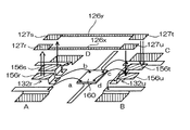
図8に、配線状態の説明図を示す。第2実施形態に係る圧電発振器は、IC160の端子bと実装端子Bとを接続するため、一対の配線用リード132r、132uを上側リードフレーム130に形成し、各配線用リード132r、132uを上側に立ち上げて一対の配線端子156r、156uを形成し、IC端子bに配線用リード132rを接続するとともに、実装端子Bに配線用リード132uを接続し、一対の配線端子156r、156uにそれぞれ接続される一対の電極パッド127r、127uと、一対の電極パッド127r、127uを相互に接続する配線パターン126xとを、圧電振動子に形成したものである。なお、第1実施形態と同様の構成となる部分については、その説明を省略する。
Next, a second embodiment will be described.
FIG. 8 shows an explanatory diagram of the wiring state. In the piezoelectric oscillator according to the second embodiment, in order to connect the terminal b of the
第2実施形態では、IC160の上面の各端子が順にa、b、c、dの機能を有するのに対して、実装端子には順にA、D、C、Bの機能を割り当てる場合を考える。なお、汎用のICを流用しながら、実装基板の電極に合わせて実装端子の機能を割り当てると、かかる場合が発生しうるのである。ここで、b−B間およびd−D間をワイヤボンディングにより接続すると、ワイヤが交差して短絡するおそれがある。したがって、これらの端子間をワイヤボンディングで配線することはできない。そこで第2実施形態では、IC端子から実装端子への配線パターン126を、圧電振動子のパッケージに形成する。
In the second embodiment, each terminal on the upper surface of the
図7に、第2実施形態に係る圧電発振器を分解した状態の斜視図を示す。第2実施形態でも、2枚のリードフレーム130、140を重ね合わせて積層リードフレーム150を形成する。上側リードフレーム130の四方には接続用リード132を形成し、その外側部分を上側に立ち上げて接続端子136を形成する。そして、図7の奥行方向における各接続用リード132の中間部には、配線用リード152を形成する。さらに、配線用リード152の外側部分を上側に立ち上げて、配線端子156を形成する。なお第2実施形態では、各接続端子136の中間部に、2個の配線端子156を並べて形成する。一方、下側リードフレーム140の四方には実装用リード142を形成し、その外側部分を下側に立ち上げて実装端子146を形成する。
FIG. 7 shows a perspective view of a state where the piezoelectric oscillator according to the second embodiment is disassembled. Also in the second embodiment, the
一方、圧電振動子110におけるパッケージ120の裏面の四隅には、外部電極124を形成する。そして、図7の奥行方向における各外部電極124の中間部に、電極パッド127を形成する。なお第2実施形態では、各外部電極124の中間部に、2個の電極パッド127を並べて形成する。また、図7の左右方向に配置された電極パッド127を相互に接続する配線パターン126を形成する。なお第2実施形態では、2本の配線パターン126を並べて形成する。なお、配線パターンは必ずしもパッケージ裏面に形成する必要はなく、パッケージ120の側面や内部に形成してもよい。
On the other hand,
そして、図8に示すように、IC160と各リードとを以下のようにして接続する。なお図8は、積層リードフレームの接続端子および圧電振動子の外部電極を省略して記載している。まず、IC端子aおよび実装端子A、ならびにIC端子cおよび実装端子Cを、ワイヤボンディングにより電気的に接続する。また、IC端子bは配線用リード132rに、実装端子Bは配線用リード132uに、それぞれワイヤボンディングにより接続する。ここで、圧電振動子を積層リードフレームに実装し、電極パッド127rを配線端子156rに、電極パッド127uを配線端子156uに接続すれば、パッケージの裏面に形成した配線パターン126xを介して、IC端子bと実装端子Bとが電気的に接続される。同様に、IC端子dは配線端子156tに、配線端子156sは実装端子Dに、それぞれ接続する。ここで、圧電振動子を積層リードフレームに実装し、電極パッド127tを配線端子156tに、電極パッド127sを配線端子156sに接続すれば、パッケージの裏面に形成した配線パターン126yを介して、IC端子dと実装端子Dとが電気的に接続される。
Then, as shown in FIG. 8, the
以上に詳述した第2実施形態に係る圧電発振器では、実装端子の機能の割り当て順序に対してIC端子の機能の割り当て順序が異なる場合であっても、対応する端子間を電気的に接続することができる。その結果、実装端子の機能の割り当て順序が異なる圧電発振器の間においても、同種のICを流用することが可能になる。したがって、ICの種類が削減され、製造コストおよび製品コストを削減することができる。 In the piezoelectric oscillator according to the second embodiment described in detail above, even when the function assignment order of the IC terminals is different from the function assignment order of the mounting terminals, the corresponding terminals are electrically connected. be able to. As a result, it is possible to divert the same type of IC even between piezoelectric oscillators having different assignment orders of functions of mounting terminals. Therefore, the types of ICs can be reduced, and manufacturing costs and product costs can be reduced.
図10は、第3実施形態に係る下側リードフレームの平面図である。この下側リードフレーム40Aは、図3(1)に示した上側リードフレーム30とともに積層リードフレームを構成する。第3実施形態の下側リードフレーム40Aは、実装用リード42Aが図3(2)に示した第1実施形態の下側リードフレーム40の実装用リード42と異なっているが、その他は下側リードフレーム40と同じである。すなわち、下側リードフレーム40Aは、各実装用リード42Aの実装端子46Aが傾斜部45の図10の左右方向における長さより大きく形成してあって、傾斜部45より枠部41の短辺側に突出した押え代170を有する。この押え代170は、下側リードフレーム40Aが上側リードフレーム30とともに積層フレームにされ、実装された圧電振動子10とIC60とを樹脂封止するときに、金型の上型によって下方に押圧される。図11は、樹脂パッケージ70を形成する金型を模式的に示したものである。
FIG. 10 is a plan view of the lower lead frame according to the third embodiment. The
図11(1)に示したように、上型172には、下側リードフレーム40Aに設けた4つの押え代170に対応して4つの押圧凸部174が設けてある。これらの押圧凸部174は、樹脂パッケージ70を形成する際に、実装用リード42Aの押え代170を上方から押圧し、実装端子46Aの主面(下面)を下型176の上面178に密着させる。このため、樹脂パッケージ70を形成する際に、樹脂が実装端子46Aの主面に付着するのを防止することができ、主面に付着した樹脂を除去する工程を省略することができる。なお、上型172と下型176とは、押圧凸部174が形成されていない部分においては、同図(2)に示したように、調整端子54の高さ位置で合わせるようになっている。
As shown in FIG. 11A, the
下側リードフレーム40Aの実装用リード42Aは、上記のようにして樹脂パッケージ70を形成したのち、樹脂パッケージ70を積層リードフレーム(下側リードフレーム40Aの枠部41)から切り離す切断工程において、図10の2点鎖線に示した切断線49Aによって切断され、押え代170が切り落とされる。ただし、押え代170は、図10に示してあるように、実装端子46Aの先端部が樹脂パッケージ70の側面から少し(例えば0.1〜0.2mm程度)突出するように切断される。
The mounting lead 42A of the
図12は、圧電発振器(樹脂パッケージ70)を積層リードフレームから切り離すときの、押え代170の切断状態を模式的に示したものである。樹脂パッケージ70を形成された積層リードフレームは、例えば切断機の下刃190の上に配置され、上刃192が矢印194のように下降することによって押え代170が切断される。このとき、積層リードフレームは、実装端子46Aが所定の長さdだけ樹脂パッケージ70から突出して押え代170が切断されるように位置決めする。このようにして押え代170を切断することにより、積層リードフレームの位置ずれが生じて同図の1点鎖線196の位置で切断される場合であっても、実装端子46Aの側面(端面)が樹脂パッケージ70から露出するため、はんだフィレットを目視でき、接合状態を容易に確認することができる。
FIG. 12 schematically shows a cut state of the
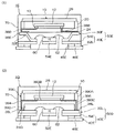
図13は、積層リードフレームから切り離された実装端子46Aを備えた圧電発振器180を示したものであって、(1)は圧電振動子10とIC60との実装状態を模式的に示したものであり、(2)は上面図、(3)は底面図である。ただし、図13においては、調整端子54が左右に4本ずつ設けられた場合を示している。この圧電発振器180は、はんだメッキされた実装端子46Aの先端部が樹脂パッケージ70の側面から突出している。したがって、圧電発振器180は、図14(1)に示したように、実装端子46Aを実装基板182の電極184にはんだ186によって接合したときに、実装端子46Aがはんだメッキしてあるため、はんだ186がせり上がって実装端子46Aの突出部を覆ってフィレットを形成する。このため、圧電発振器180は、実装基板182への接合(実装)状態を目視によって容易に確認することができる。また、はんだ186が実装端子46Aの突出部を覆うため、実装強度を向上することができる。なお、押え代170は、調整端子54を切断するときに切断してもよい。また、実装端子46Aは、樹脂パッケージ70の長辺に沿った部分を突出させるようにしてもよいし、L字状に突出させてもよい。
FIG. 13 shows a
すなわち、実装端子46Aは、図14(2)に示したように、2辺の端部を樹脂パッケージ70から突出させてもよい。このようにすることにより、実装端子46Aは、はんだ186によって覆われる面積が大きくなり、実装基板182への実装強度を向上することができる。なお、同図に示したように、積層リードフレームの下側リードフレーム40Aに調整端子54を形成するとともに、上側リードフレーム30に調整端子54Aを形成してもよい。さらに、調整端子は、上側リードフレームのみに形成してもよい。
That is, the mounting
図15は、第4実施形態に係る下側リードフレームを示したものであって、(1)は平面図、(2)は(1)のC−C線に沿った断面図である。この下側リードフレーム40Bは、図3(1)に示した上側リードフレーム30とともに積層リードフレームを構成する。この第4実施形態の下側リードフレーム40Bは、図15(2)に示してあるように、実装用リード42Bが傾斜部を有しておらず、実装端子46Bとパッド44とが同一平面内に形成してあり、調整端子54と同じ高さに形成される。このため、下側リードフレーム40Bは、実装端子46Bを調整端子54より下側に位置させるための曲げ加工を必要とせず、下側リードフレーム40Bを形成する工程の簡素化が図れる。したがって、図15に示した下側リードフレーム40Bと、図3(1)に示した上側リードフレーム30とを重ね合わせて形成する積層リードフレームは、一方側のリードフレーム(上側リードフレーム30)の接続用リード32だけが、積層面と反対側に折曲された積層リードフレームとなる。このため、積層リードフレームの高さ方向の寸法を小さくでき、圧電発振器の薄型化が図れる。
FIGS. 15A and 15B show a lower lead frame according to the fourth embodiment. FIG. 15A is a plan view, and FIG. 15B is a cross-sectional view taken along line CC in FIG. The
第4実施形態の下側リードフレーム40Bを用いた積層リードフレームにおける樹脂封止は、図16のようにして行なわれる。すなわち、樹脂パッケージ70Bを形成する上型200と下型202とは、実装端子46Bの高さの位置で合わせるようになっている。そして、下型202には、キャビティを形成する面に凹部204が設けてあり、樹脂パッケージ70Bの下端面206が調整端子54、すなわち実装端子46Bの主面の下方に位置するようになっている。つまり、樹脂パッケージ70Bは、各実装端子46Bと対応した位置に凹部208が形成され、この凹部208の天井面に実装端子46Bが設けられた形状をなす。これは、切断したのちの調整端子54が実装基板に接触して実装基板に設けた配線パターンや他の部品と短絡したりするのを防止するためである。なお、凹部208の高さは、調整端子54が実装基板の表面に接触しない高さであればよく、例えば0.1mm程度であってよい。
Resin sealing in the laminated lead frame using the
図17は、実装端子46Bを有する圧電発振器210を示したものであって、(1)は圧電振動子10とIC60との実装状態を示す模式図であり、(2)は平面図、(3)は底面図である。この圧電発振器210は、例えば図18に示したようにして実装基板182に実装することができる。この実装方法は、まず、図18(1)に示したように、圧電発振器210の各実装端子46Bにはんだボール212を設ける。そして、はんだボール212を実装基板182の電極184の上に配置する。その後、同図(2)に示したように、はんだボール212を溶融することにより、圧電発振器210を実装基板182に実装することができる。
FIG. 17 shows a
このようにして実装基板182に実装された圧電発振器210は、実装端子46Bが凹部208の天井面に設けてあるため、実装端子46Bと実装基板182との間に間隙gが形成される。そして、この間隙gは、はんだボール212を構成していたはんだ220によって埋められることになる。このため、間隙gがはんだ220によって埋められているか否かを目視によって観察することにより、実装(接合)状態の良否を容易に判断することができる。
In the
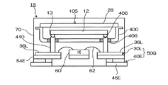
図19は、第5実施形態を説明する分解斜視図であって、図1に対応した図である。ただし、図19においては、積層リードフレーム50Eが図1に対して平面内で90℃回転した状態となっている。図19(1)において、圧電発振器1Eは、パッケージ20内に圧電振動片12を収納した圧電振動子10と、発振回路などが形成してあるIC60とが積層リードフレーム50Eによって一体化することにより形成される。積層リードフレーム50Eは、一方側となる上側リードフレーム30Eと、他方側となる下側リードフレーム40Eとからなる。これらの上側リードフレーム30Eと下側リードフレーム40Eとは、圧電発振器1Eがより小型化され、モールド樹脂との接触面積が小さくなることによる接合強度の低下を防止する工夫がしてある。すなわち、各リードフレーム30E、40Eは、それぞれのリードが異形に形成してあって、樹脂との接合強度をできるだけ向上させるようにしてある。
FIG. 19 is an exploded perspective view for explaining the fifth embodiment and corresponds to FIG. However, in FIG. 19, the
上側リードフレーム30Eによって形成した4つの接続用リード32Eは、それぞれパッド部34Eと傾斜部35Eと接続端子36Eとを有する。そして、接続端子36Eには、パッケージ20の底面に設けた本図に図示しない外部電極を介して、圧電振動子10が実装(接合)される。また、接続用リード32Eは、異形に形成してあって、傾斜部35Eに切り欠き(凹部)37Eを有する。この切り欠き37Eは、樹脂パッケージ70を形成する際に、樹脂を入り込ませるためのもので、切り欠き37Eに入り込んだ樹脂のアンカー効果により、接続用リード32Eが樹脂パッケージから抜けて脱落するのを防止する。
The four connection leads 32E formed by the
下側リードフレーム40Eによって形成した実装用リード42Eは、図19(1)のD−D線に沿った断面図である同図(2)に示したように、パッド部44Eと傾斜部45Eと実装端子46Eとを有する。そして、実装用リード42Eは、異形に形成してあり、実装端子46Eより基端側となる傾斜部45Eからパッド部44Eにかけてとパッド部44Eとに、樹脂パッケージ70を構成する樹脂を入り込ませる切り欠き(凹部)48Eが設けてある。また、樹脂パッケージ70は、実装端子46Eの主面230が露出するように形成される。したがって、実装端子46Eは、主面230がはんだを介して実装基板の電極パターンに接合できるようになっている。なお、この実施形態においては、図19(1)の右側の実装用リード42Eは、実装基板のグランド端子に接続するようになっていて、ダイパッド52Eと一体に形成してある。
The mounting
下側リードフレーム40Eによって形成した調整端子54Eは、この実施形態の場合、図19(1)の左右方向に位置する実装用リード42E、42E間に配置してある。調整端子54Eは、先端端子部51Eと、先端端子部51Eと一体の基端部53Eとからなり、T字状に形成してある。すなわち、調整端子54Eは、基端部53Eの幅(図9(1)の左右方向の長さ)を有するリード片の先端側の両側を切り欠いて切り欠き部57Eを形成してT字状に形成したものである。なお、この実施形態に示した調整端子54Eは、圧電発振器1Eの調整工程が終了し、先端端子部51Eの先端側の不要部が切断された状態を示しており、図19(3)に示したように、基端部53Eが樹脂パッケージ70の内部に埋め込まれる。また、実装用リード42Eの切り欠き48Eを形成している凸部61、63は、実施形態の場合、積層リードフレーム50Eを樹脂封止したときに、先端部が樹脂パッケージ70から突出した状態で切断され、調整端子として利用される。
In this embodiment, the
このようになっている第5実施形態においては、接続用リード32E、実装用リード42Eに切り欠き37E、48Eが形成されているため、これらの切り欠きに37E、48Eに樹脂パッケージ70を構成するモールド樹脂が入り込む。このため、接続用リード32E、実装用リード42Eは、樹脂パッケージ70から抜けるのを防止することができ、接合強度を大きくできる。また、調整端子54Eは、樹脂に埋め込まれる基端部53Eが先端端子部51Eより幅が広く形成してあるため、樹脂パッケージ70から抜けることがない。したがって、圧電発振器1Eは、樹脂パッケージの樹脂とリード、端子との接合部が剥離するのを防止することができ、耐衝撃性を向上することができる。
In the fifth embodiment thus configured, the
図20は、第6実施形態に係る圧電発振器の分解斜視図である。この第6実施形態の圧電発振器1Fは、積層リードフレーム50Fを構成している下側リードフレーム40Fが第5実施形態の下側リードフレーム40Eと異なっていて、他は第5実施形態と同様である。この第6実施形態に係る下側リードフレーム40Fは、実装用リード42Fが傾斜部を有していない。すなわち、実装用リード42Fは、折曲されておらず、パッド部44Fと実装端子46Fとの上面が同一平面内に位置している。ただし、実装用リード42Fは、図20(1)のE−E線に沿った断面図である同図(2)に示したように、基端側となるパッド部44Fが実装端子46Fより薄肉に形成してある。このため、実装用リード42Fは、実装端子46Fの主面230とパッド部44Fの下面232との間に段差部234が形成されている。また、パッド部44Fには、第5実施形態に示したと同様の切り欠き48Eが設けてある。下側リードフレーム40Fの他の構成は、第5実施形態と同様である。なお、実装用リード42Fは、プレスによる塑性加工やエッチングなどによってパッド部44Fを薄肉化することにより、容易に形成することができる。
FIG. 20 is an exploded perspective view of the piezoelectric oscillator according to the sixth embodiment. The
このようになっている第6実施形態の積層リードフレーム50Fは、下側リードフレーム40Fの実装用リード42Fがパッド部44Fと実装端子46Fとの間に傾斜部を形成しないため、上側リードフレーム30Eの接続用リード32Eのみが積層面と反対側に折曲される。このため、積層リードフレーム50Fは、実装端子46Fを大きくすることができる。したがって、実装端子46Fは、実装基板との接合面積が大きくなり、実装基板との接合強度を向上することができる。また、積層リードフレーム50Fは、実装用リード42Fに傾斜部が設けられていないため、厚み方向の寸法が小さくなり、圧電発振器1Fの薄型化を図ることができる。
In the
さらに、実装用リード42Fは、傾斜部を有していないため、小型化された場合であっても、加工時や衝撃力が作用したときに破断するようなことがない。すなわち、圧電発振器が小型化、薄型化されるのに伴って、実装用リードも小型、薄肉化される。そして、実装端子を実装用リードの曲げ加工(フォーミング)によって形成する場合、傾斜部が他の部分より肉厚が薄くなる。したがって、実装用リードを曲げ加工して実装端子を形成した場合、実装用リードの曲げ加工時や、圧電発振器に衝撃力が作用して樹脂との剥離が生ずると、傾斜部において破断するおそれがある。これに対し、実施形態の実装用リード42Fは、傾斜部を有しないため、このような破断を生ずるおそれがない。
Furthermore, since the mounting
なお、下側リードフレーム40Fは、実装端子46Fの部分のみを厚肉に形成し、ダイパッドを含めて実装端子以外の部分をエッチングなどにより薄肉にしてもよい。この場合、実装端子46Fの主面230が、図20(2)に示したように、薄肉にした他の部分の下面より下方となるようにする。これにより、実装端子を折曲して形成しなくとも、実装端子46Fの主面230を露出させて樹脂モールドをしたときに、実装端子46F以外の薄肉の不要な部分は樹脂パッケージ70内に封止される。したがって、実装端子46Fを実装基板に接合したときに、他の部分が実装基板の配線パターンなどと短絡するようなことがなく、圧電発振器の薄型化を図ることができる。
In the
なお、第6実施形態において、接続用リード32Eの代わりに、同図(3)に示したような接続用リード32Fにしてもよい。この接続用リード32Fは、パッド部34Fと接続端子36Fとの間に傾斜部が設けられておらず、パッド部34Fと接続端子36Fとの下面が同一平面内に位置している。そして、接続用リード32Fは、パッド部34Fの肉厚が接続端子36Fの肉厚より薄くなっている。このため、パッド部34Fの上面236が接続端子36Fの主面238より低くなっている。このような接続用リード32Fは、接続端子36Fの面積を大きくすることができ、圧電振動子10との接合強度を大きくすることができる。また、圧電発振器の薄型化が図れる。この接続用リード32Fは、実装用リード42Fと同様にして形成することができる。そして、この接続端子36Fを有する上側リードフレーム30Eは、接続端子36F以外の部分のすべてを接続端子36Fより薄く形成することができる。
In the sixth embodiment, instead of the connection lead 32E, a
図21は、第7実施形態に係る圧電発振器の分解斜視図である。この圧電発振器1Gは、積層リードフレーム50Gを構成している下側リードフレーム40G、特に実装用リードの実装端子が第5実施形態の下側リードフレーム40Gの実装端子46Eと異なっている。他は、第5実施形態と同様である。この第7実施形態に係る実装用リード42Gは、図21(1)のF−F線に沿った断面図である同図(2)に示したように、パッド部44Eと傾斜部45Eと実装端子46Gとを有する。そして、実装端子46Gは、主面230に凸部240が形成してある。また、実装端子46Gは、主面230と反対側の樹脂との接合面242の、凸部240と対応した位置に凹部244が形成してある。これらの凸部240と凸部244とは、実装端子46Fをプレス成形することにより、容易に形成することができる。
FIG. 21 is an exploded perspective view of the piezoelectric oscillator according to the seventh embodiment. This piezoelectric oscillator 1G is different from the mounting terminal 46E of the
このようになっている実装端子46Gは、主面230に凸部240が形成されているため、実装基板に接合したときに、はんだとの接触面積が大きくなるとともに、凸部240によるアンカー効果により、実装基板との接合強度を向上することができる。また、実装端子46Gは、樹脂との接合面242に凹部244が形成してあるため、樹脂との実質的な接合面積が大きくなるとともに、凹部244に樹脂が入り込むため、樹脂との接合強度を高めることができる。
Since the mounting terminal 46G thus formed has the
なお、実装端子は、図21(1)の右側に示した実装用リード42Hのように形成してもよい。すなわち、実装用リード42Hは、図21(1)のG−G線に沿った断面図である同図(3)に示したように、実装端子46Hの主面230に凹部246が形成してある。また、実装端子46Hは、主面230の反対側の樹脂との接合面242に凸部248が形成してある。主面230側の凹部246と、接合面242側の凸部248とは対応していて、プレスによる曲げ加工などにより形成される。このように形成した実装端子46Hは、同図(2)の実装端子46Gと同様の効果を得ることができる。
The mounting terminal may be formed like the mounting lead 42H shown on the right side of FIG. That is, the mounting
さらに、実装用リードは、図22のように形成することができる。図22に示した実装用リード42Jは、厚さtのリード片のパッド部44Jの下面側と、実装端子46Jの上面側とをエッチングし、クランク状に形成したものである。この実装用リード42Jにおいても、実装端子46Jの面積を大きくすることができ、厚み方向の寸法を小さくすることができる。
Furthermore, the mounting leads can be formed as shown in FIG. The mounting lead 42J shown in FIG. 22 is formed in a crank shape by etching the lower surface side of the
なお、第7実施形態においては、実装端子に凸部または凹部を1つ設けた場合について説明したが、これらは複数設けることができる。また、接続用リード32Eに代えて、図23に示した接続用リードのように形成してもよい。図23(1)に示した接続用リード32Gは、接続端子36Gの、圧電振動子10を接合する主面238に凸部250が設けてある。そして、接続端子36Gは、主面238と反対側の樹脂との接合面に凹部(図示せず)が形成してある。このように形成した接続端子36Gは、圧電振動子10との接合強度、および樹脂パッケージの樹脂との接合強度を向上することができる。
In the seventh embodiment, the case where one protrusion or recess is provided on the mounting terminal has been described, but a plurality of these can be provided. Further, instead of the
図23(2)に示した接続用リード32Hは、接続端子36Hの主面238に凹部252が形成してあり、その反対側の樹脂との接合面に凸部254が形成してある。また、同図(3)に示した接続用リード32Jは、接続端子36Jの主面238に凹部256が形成され、その反対側の面に凸部258が形成されている。そして、凹部256は、接続端子36Jの先端側において開口していて、U字状をなしている。これらの接続端子36H、36Jも接続端子36Gと同様の効果が得られる。
In the
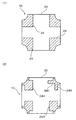
ところで、圧電発振器は、電子機器の小型、薄型化に伴って、より一層小型、薄型化の要求が強くなっている。このため、図19に示した第5実施形態においては、実装用リードを異形に形成して樹脂との接合強度の向上を図っているが、第5実施形態のような実装用リードを形成できない場合も予想される。すなわち、実装用リードを図24(1)に示した実装用リード42Eのように形成できず、同図(2)に示した実装用リード260のようにしか形成できない場合が考えられる。この実装用リード260は、実装用リード42Eに形成した樹脂との引っ掛かりを図る凸部63Eが形成されていないため、実装用リード260の面と平行な方向の力に対していくぶん弱くなる。そこで、実装端子46Eを異形に形成して樹脂との接合強度の向上を図る。図25は、その一例を示したものである。なお、図25においては、実装リード260の実装端子以外の他の部分は省略してある。
By the way, with respect to piezoelectric oscillators, as electronic devices become smaller and thinner, there is an increasing demand for further reduction in size and thickness. For this reason, in the fifth embodiment shown in FIG. 19, the mounting lead is formed in an irregular shape to improve the bonding strength with the resin, but the mounting lead as in the fifth embodiment cannot be formed. Cases are also expected. That is, it is conceivable that the mounting lead cannot be formed like the mounting
図25(1)に示した実装端子262は、貫通孔262Aが形成してある。この実装端子262は、貫通孔262Aに樹脂パッケージ70を形成するモールド樹脂が入り込むため、アンカー効果が得られて樹脂との接合強度を向上することができる。なお、同図(2)に示した実装端子264のように、貫通孔に代えて、樹脂との接合面に凹部264Aを形成してもよい。
The mounting
図25(3)〜(7)は、実装端子の辺部に切り欠き(凹部)を形成した例を示したものである。図25(3)に示した実装端子266は、対向する2辺の中央部に矩形状の切り欠き266Aを形成したものである。また、同図(4)に示した実装端子268は、C字状の切り欠き268Aを形成したものである。そして、図25(5)に示した実装端子270は、1つの辺の先端側に矩形状の切り欠き270Aを形成したものである。さらに、同図(6)に示した実装端子272は、実装端子272の先端側の2つの角部を、円弧状または矩形状に切除して切り欠き272Aを形成したものである。同図(7)に示した実装端子274は、先端側の辺に円弧状またはU字状の切り欠き274Aを形成したものである。
25 (3) to 25 (7) show examples in which notches (recesses) are formed in the side portions of the mounting terminals. The mounting
これらの実装端子266〜274は、いずれも切り欠きに樹脂が入り込んで樹脂と引っ掛かるため、実装端子の面と平行な方向に作用する力に対する強度を向上することができる。なお、積層リードフレームを樹脂パッケージ70に封止したときの、樹脂パッケージ70の下面に露出した実装端子266、270、272、274の状態を図26に示した。
Since all of these mounting
図27は、実装端子の厚み方向(上下方向)の接合強度の向上を図った例を示したものである。図27(1)に示した実装端子276は、側面に凹部276Aが形成されて厚み方向に段部を有している。すなわち、実装端子276は、主面276B側の幅が反対側より狭くなっている。また、同図(2)に示した実装端子278は、側面の厚み方向中間部に凸部278Aが帯状に形成してある。なお、各凸部278Aは、連続して形成してもよいし、複数に分割されていてもよい。図27(3)に示した実装端子280は、側面が厚み方向に傾斜した傾斜面280Aとなっている。この傾斜面280Aは、主面280B側の幅が反対側、すなわち樹脂パッケージ70の中心側より狭くなるように形成してある。これらの実装端子276、278、280は、いずれも実装基板に接合した場合に、実装端子の厚み方向(樹脂パッケージ20の上下方向)に力が作用したときに、樹脂から剥離するのが防止される。
FIG. 27 shows an example in which the bonding strength in the thickness direction (vertical direction) of the mounting terminal is improved. The mounting
なお、実装端子276、278は、プレスやエッチングによって容易に形成することができる。また、実装端子280の傾斜面280Aは、図28のようにして形成することができる。図28(1)に示した方法は、切断加工刃284を矢印286のように、リードフレーム282に対して所定の角度θを持って前進させて切断する。この方法は、各傾斜面280Aを別々に形成する必要がある。これに対して、同図(2)は、各傾斜面280Aを同時に形成することができる。すなわち、図28(2)に示した方法は、傾斜面280Aを形成する切断加工刃288(288A、288B)の刃部290幅Lが、リードフレーム282の厚みtより広くなっている。そして、各切断加工刃288を同時に降下させ、刃部290の先端がリードフレーム282を貫通した段階で止めることにより、複数の傾斜面280Aを同時に形成することができる。
Note that the mounting
図29は、第8実施形態の説明図である。図29(1)に示したように、この第8実施形態に係る圧電発振器350は、樹脂パッケージ70の底面に4つの実装端子352と複数(実施形態の場合、4つ)の調整端子354とを設け、本図に図示しない実装基板に接合(実装)できるようにしてある。これらの調整端子354は、同図(2)に示したように、実装端子352と同様に側面が樹脂パッケージ70から露出していてもよい。このようになっている圧電発振器350は、調整端子354が実装基板に設けたダミー端子などにはんだ等によって接合される。したがって、圧電発振器350は、実装端子352と調整端子354とによって実装基板に接合されるため、実装強度が向上し、耐衝撃性を大幅に高めることができる。
FIG. 29 is an explanatory diagram of the eighth embodiment. As shown in FIG. 29 (1), the
図30は、第9実施形態の説明図である。この実施形態に係る圧電発振器360は、図30(1)に示したように、調整端子362(362A〜362D)が樹脂パッケージ70の側面から突出して形成してある。これらの調整端子362のうち、両側の調整端子362A、362Dは、実装用リードの一部によって形成され、実装端子352と一体となっている。そして、調整端子362は、圧電発振器360の特性調整、検査後、同図(2)に示したように、下方に折曲されて実装基板に実装可能にされる。調整端子362の折曲は、調整端子362A、362Bに示したように、樹脂パッケージ70の下側に折り込んでJ端子としてもよく、調整端子362Cのようにガルウイングとしてもよい。また、調整端子362Dのように樹脂パッケージ70から突出した部分を切断してもよい。
FIG. 30 is an explanatory diagram of the ninth embodiment. In the
このように、第9実施形態に係る圧電発振器360は、使用環境、使用条件に応じて調整端子(実装用リードの一部によって形成したものを含む)362を実装基板に接合することができ、実装に対する柔軟性を備え、実装強度の向上を図ることができる。なお、調整端子362は、図30(3)に示したように、先端部の幅を広くしてもよい。このように、先端部の幅を広くすると、検査・調整装置のプローブの接触を容易に行なえるとともに、実装基板に接合した場合に、より接合強度を向上することができる。
As described above, the
図31は、第10実施形態に係る積層リードフレーム部の斜視図である。第10実施形態に係る積層リード50Kは、上側リードフレーム30Kと下側リードフレーム40Kとを積層して形成してある。下側リードフレーム40Kは、実装基板に実装するための斜線に示した4つの実装端子46Kを形成している。そして、下側リードフレーム40Kは、積層リードフレーム50Kにされて枠部から切断されたときに、実装用リードが平板上の実装端子46Kのみからなっていて、折曲部を有していない。
FIG. 31 is a perspective view of the multilayer lead frame portion according to the tenth embodiment. The
一方、上側リードフレーム30Kは、接続端子36Eを有する接続用リード32Eが形成してあるとともに、IC60を実装するためのダイパッド366と複数の調整端子368とを形成している。調整端子368は、基端側の幅が先端側より広いT字状に形成してある。そして、IC60は、上側リードフレーム30Kに設けたダイパッド266の上面に実装してある。また、本図に図示しない圧電振動子は、上側リードフレーム30Kの接続端子36Eに実装される。この上側リードフレーム30Kは、接続用リード32Eが下側リードフレーム40Kとの積層面と反対側、すなわち上側に折曲してある。下側リードフレーム40Kは、前記したように折曲されていない。このため、実装端子46Kの上下方向の位置は、上面が上側リードフレーム30Kのダイパッド366の下面と接する位置となっている。
On the other hand, the
すなわち、積層リードフレーム50Kは、上側リードフレーム30Kの接続用リード32Eのみが積層面と反対側に折曲されている。このため、積層リードフレーム50Kは、高さ方向の寸法を小さくすることができ、圧電発振器の薄型化を図ることができる。この積層リードフレーム50Kを樹脂封止した状態における図31のβ−β線に沿った矢視図を図32(1)に模式的に示した。なお、同図(2)は、第10実施形態の変形例を示したものであって、下側リードフレーム40Kにダイパッド52Kを設け、IC60を下側リードフレーム40Kに実装した状態を示している。そして、同図(3)は、第10実施形態と対比するために、第5実施形態を示す図19のα−α線に沿った矢視図を模式的に示したものである。
That is, in the
図33は、第10実施形態の他の変形例を示したものである。この変形例は、下側リードフレーム40Kの実装端子46Kの先端部を上側に折曲したものである。すなわち、図33(1)に示した変形例は、実装端子46Kの先端が樹脂パッケージ70の側面から突出していて、その突出した部分が樹脂パッケージ70の外側面に沿って上方に折曲された折曲部370となっている。このように折曲部370を形成することにより、大きなフィレットが形成され、実装の良否を目視によって容易に確認することができるとともに、実装強度を向上することができる。なお、同図(2)に示したように、実装端子46Kの折曲部370の外面が樹脂パッケージ70の側面と一致するように、折曲部370を樹脂パッケージ70内に配置してもよい。
FIG. 33 shows another modification of the tenth embodiment. In this modification, the tip of the mounting terminal 46K of the
第10実施形態においては、上側リードフレーム30Kの接続用リード32Eを折曲し、下側リードフレーム40Kのリードを折曲しない場合であったが、逆に上側リードフレームのリードを折曲せず、下側リードフレームのリードを折曲してもよい。図34は、その例を第11実施形態として模式的に示した断面図である。図34(1)に示したように、積層リードフレーム50Lは、接続端子36Lを形成している上側リードフレーム30Lと、下側リードフレーム40Lとから構成してある。上側リードフレーム30Lは、接続用リードが折曲されておらず、積層リードフレーム50Lにされて枠部から切断されたときに、接続端子36Lのみからなっている。一方、下側リードフレーム40Lは、IC60を実装するダイパッド52Lと、実装用リード42L、調整端子54Lとを有する。実装用リード42Lは、パッド44Lと傾斜部45Lと先端部の実装端子46Lとを有する。そして、実装用リード42Lは、先端側が積層面と反対側(下方側)に折曲してあって、ダイパッド52Lの下面に実装したIC60と、パッド44Lとを電気的に接続するワイヤ62の配置スペースを形成している。この第11実施形態においても、一方のリードフレームだけを折曲しているため、積層リードフレーム50Lの上下方向の寸法を小さくすることができ、圧電発振器の薄型化を図ることができる。
In the tenth embodiment, the
図34(2)は、第11実施形態の変形例を示したものである。すなわち、この変形例は、上側リードフレーム30Lにダイパッド366Lを設け、このダイパッド366Lの下面にIC60を実装したものである。
FIG. 34 (2) shows a modification of the eleventh embodiment. That is, in this modification, a
図35は、第11実施形態の他の変形例を示したものである。図35(1)に示した変形例は、実装用リードを樹脂パッケージ70から突出させて形成し、その突出部372を下側に折曲したものである。そして、同図左側に示した実装用リード42LaはJリードに形成し、先端の実装端子46Laを樹脂パッケージ70の下面に配置したものである。また、同図右側に示した実装用リード42Lbは、ガルウイングとしたもので、実装端子46Lbを樹脂パッケージ70の外部に配置したものである。
FIG. 35 shows another modification of the eleventh embodiment. In the modification shown in FIG. 35A, the mounting lead is formed to protrude from the
図35(2)に示した変形例は、実装端子の先端部を上方に折曲したものである。そして、同図の左側に示した変形例は、実装端子46Ldの先端折曲部374の外面が樹脂パッケージ70の側面と一致するように、折曲部374が樹脂パッケージ70内に配置してある。また、同図の右側に示した変形例は、折曲部374が樹脂パッケージ70の外側に配置してある。図35に示したこれらの変形例においても、圧電発振器を実装基板に実装したときに、大きなフィレットが形成され、実装の良否を目視によって容易に判別でき、実装強度を向上することができる。
In the modification shown in FIG. 35 (2), the tip of the mounting terminal is bent upward. In the modification shown on the left side of the figure, the
図36は、第12実施形態の分解斜視図である。この第12実施形態に係る圧電発振器1Mは、図36の右側に示しているように、下側リードフレーム40Eのダイパッド52Eと一体のタイバー376と、上側リードフレーム30Eの1つの接続用リード32Eaとをワイヤ62aによって電気的に接続したものである。この実施形態は、圧電振動子10の外部端子24とダイパッド52Eとを同電位にしたほうが都合のよい場合があり、このような場合に有効である。なお、上側リードフレームの接続用リードと下側リードフレームのタイバーとの電気的接続は、図37のようにして行なってもよい。
FIG. 36 is an exploded perspective view of the twelfth embodiment. As shown on the right side of FIG. 36, the
図37(1)に示した例は、上側リードフレームに、下側リードフレーム40Eに形成したタイバー376の上面に接する接続用リード32Mを形成する。すなわち、接続用リード32Mは、基端側の接合部34Mの端部がタイバー376の上部に位置し、下面がタイバー376の上面に接するようになっている。そして、接合部34Mとタイバー376とは、積層リードフレームを形成する際に、スポット溶接によって接合される。しかし、両者の接合は、シリコン系またはエポキシ系の導電性接着剤やはんだなどの導電性部材によって接合してもよい。
In the example shown in FIG. 37A, the
図37(2)に示した例は、電子部品378を介して接続した例を示したものである。この場合、上側リードフレームに形成した接続用リード32Maは、基端側の接合部34Maがタイバー376の側方に位置するように形成される。そして、接続用リード32Maの接合部34Maとタイバー376とは、コンデンサや抵抗などの電子部品378を介して電気的に接続してある。
The example shown in FIG. 37 (2) shows an example of connection through an
図38は、圧電振動子10のパッケージ20の下面に形成する外部電極の変形例を示したものである。外部電極24は、通常、図38(1)に示したように、ほぼ矩形状または正方形状に形成され、キャスタレーションを挟んだ隣接する2辺がパッケージ20の辺と一致するように形成される。しかし、同図(2)に示した外部電極24Aのように、キャスタレーションを挟んだ隣接する2辺をパッケージ20の辺から離間させて形成してもよい。そして、IC60とリードフレームとを電気的に接続するワイヤ62がパッケージ20の下面に接触するおそれがある場合、同図の外部電極24Bに示したように、切り欠き380を形成し、L字状に形成してもよい。外部端子24Bのように切り欠き380を形成すると、ワイヤ62がパッケージ20に接触してもよい面積を大きくすることができ、圧電発振器の設計の自由度を増すことができる。
FIG. 38 shows a modification of the external electrode formed on the lower surface of the
図39は、調整端子の変形例を示したものである。図39(1)に示した調整端子54Nは、先端部に幅広部382を有する。圧電発振器が小型化されるのに伴って、調整端子の幅も小さくされる。このため、測定装置などのプローブを調整端子に接触させることが困難となってくる。そこで、調整端子54Nは、先端部に幅広部382を設けた。これにより、測定装置のプローブを容易に接触させることができ、特性の調整、検査を容易、迅速に行なうことが可能となる。また、図39(2)に示した調整端子54Pは、各調整端子54Pに幅広部384を設けるとともに、隣接する調整端子54Pの幅広部384を調整端子の長手方向において位置をずらして配置したものである。これにより、調整端子間のピッチが小さくなったとしても、比較的幅の広い幅広部384を形成することができる。
FIG. 39 shows a modification of the adjustment terminal. The
なお、上記各実施形態においては、IC60とリードフレームとを電気的に接続するワイヤ62の配置スペースを、リードフレームのリードを折曲することによって形成していた。例えば、図40(1)に示したように、第5実施形態に係る圧電発振器1Eは、上側リードフレーム30Eの接続用リード32Eを上側に折曲することにより、ワイヤ62の配置スペースを確保している。なお、圧電振動子10のパッケージ20の下面に形成した外部電極24は、一部をパッケージ20の側面を経由させた配線パターン386、またはビヤホール388を経由させた配線パターンを介して、圧電振動片12に形成した電極に電気的に接続してある。
In each of the above embodiments, the arrangement space of the
しかし、ワイヤ62の配置スペースを、図40(2)に示した第13実施形態のようにして形成してもよい。この第13実施形態に係る圧電発振器1Qは、積層リードフレーム50Qの上側リードフレーム30Lが平板状の接続用端子36Lのみからなっている。そして、圧電振動子10を構成している振動子パッケージ390のベース390Aがセラミックから形成してあって、底部390Bの下面周縁部にスペーサ部390Cを有している。このため、振動子パッケージ390は、底部390Bの下方にワイヤ62を配置する凹部392が形成されている。なお、スペーサ部390Cは、振動子パッケージ390の対向する2辺だけに設けてもよいし、四隅に柱状に形成してもよい。
However, the arrangement space of the
スペーサ部390Cの下面には、接続電極36Lに接合した外部電極24Qが形成してある。これらの外部電極24Qは、振動子パッケージ390の側面を経由した配線パターン394、またはビヤホール396を経由した配線パターンを介して、圧電振動片12に形成した電極に電気的に接続してある。
An
図41は、第14実施形態の断面図である。この第14実施形態に係る圧電発振器1Rは、圧電振動子10Rのベース400が金属からなるいわゆる金属パッケージとなっている。そして、ベース400の底部には、端子孔が形成してあって、この端子孔を端子部材402が貫通している。端子部材402は、下端部に外部端子(外部電極)404が形成してあり、この外部端子404が上側リードフレーム30Eの接続端子36Eに接合してある。また、端子部材402は、上下方向の中間部がケイホウ酸ガラスなどの絶縁部材406を介してベース400の底部に支持されている。そして、端子部材402は、上端がベース400内に突出し、導電性接着材13を介して圧電振動片12に設けた電極に電気的に接続してある。このように形成してある圧電発振器1Rは、ベース400が金属で形成してあるため、肉厚を薄くしても高い気密性が得られ、振動子パッケージの小型化、薄型化が図れる。したがって、圧電発振器1Rをより小型化、薄型化をすることができる。
FIG. 41 is a cross-sectional view of the fourteenth embodiment. The
図42は、第15実施形態の断面図である。第15実施形態に係る圧電発振器1Sは、圧電振動子10Sが積層リードフレーム50Qに実装してある。圧電振動子10Sは、金属ベース400の底部を貫通している端子部材410が柱状に形成してある。そして、柱状端子部材410は、ベース400の下面からの突出長さが大きくしてあって、上側リードフレーム30Lとベース400の下面との間にワイヤ62の配置空間を形成している。また、端子部材410は、下端が導電部材を介して上側リードフレーム30の接続端子36Lに接合してある。
FIG. 42 is a cross-sectional view of the fifteenth embodiment. In the
図43は、第16実施形態の説明図である。図43(1)に示した圧電発振器1Tは、樹脂パッケージ70の上面の対角位置の2箇所に凹部420、422を有する。これらの凹部420、422は、モールド成形した樹脂パッケージ70を成型金型から離間するために押し出すエジェクタピン(図示せず)によって形成される。そして、これらの凹部420、422のいずれか一方、例えば凹部420の面が鏡面に形成してあり、他方の凹部422の面が粗面に形成してあって、両者間において光の反射率が異なっている。このため、凹部420を方向確認用標識に使用することができる。すなわち、圧電発振器1Tを実装基板に実装する場合、画像処理装置を用いて実装方向を確認しながら自動的に行なわれる。そこで、凹部420の面を鏡面にして光の反射率を高くすることにより、画像処理をする際に凹部420を容易に認識することができ、これを方向確認用標識として使用することにより、圧電発振器1Tの実装の向きを容易、確実に一定にすることができる。
FIG. 43 is an explanatory diagram of the sixteenth embodiment. The piezoelectric oscillator 1T shown in FIG. 43 (1) has
なお、凹部420、422の形状は、図43(2)に示したように、円柱状であってもよいし、同図(3)に示したように、球面の一部をなすように形成してもよい。さらに、凹部420、422は、図43(4)に示したようにリッド28の上面が露出するように形成してもよい。また、凹部420と凹部422とは、相互に形状が異なっていてもよい。そして、樹脂パッケージ70の上面に形成する凹部は、3個以上であってもよい。
The
図44は、本発明の上述した実施形態に係る圧電発振器を利用した電子機器の一例として示したデジタル式携帯電話装置の概略構成図である。図44において、デジタル式携帯電話装置300は、発信者の音声を電気信号に変換するマイクロフォン308を備えている。マイクロフォン308からの電気信号は、デモデュレータ、コーデック部312においてデジタル変調され、送信部307においてRF(Radio Frequency)帯に周波数変換されたのち、スイッチ部314を介してアンテナ316に送られ、アンテナ316から基地局(図示せず)に送信される。基地局からのRF信号は、アンテナ316によって受信されたのち、スイッチ部314、フィルタ・アンプ部318を経由して受信部306に入力し、受信部306において周波数変換される。周波数変換された受信信号は、デモデュレータ、コーデック部312において音声信号に変換され、スピーカ309から出力される。
FIG. 44 is a schematic configuration diagram of a digital mobile phone device shown as an example of an electronic apparatus using the piezoelectric oscillator according to the above-described embodiment of the present invention. In FIG. 44, a digital cellular phone device 300 includes a
スイッチ314は、CPU(Central Processing Unit)301によって切替え制御され、通常時はアンテナ316を受信部306に接続し、送信時にアンテナ316を送信部307に接続する。また、CPU301は、液晶表示装置(表示部)およびキーボードからなる入出力部302、メモリ303をはじめ、デジタル式携帯電話装置300の全体の動作を制御している。メモリ303は、RAM(Random Access Memory)、ROM(Read Only Memory)からなる情報記憶手段であり、この中にデジタル式携帯電話装置300の制御プログラムや電話帳などの情報が格納してある。
The
本発明の実施形態に係る圧電発振器が応用されるものとして、例えばTCXO(Temperature Compensated Crystal Oscillator:温度補償圧電発振器)305がある。このTCXO305は、周囲の温度変化による周波数変動を小さくした圧電発振器であって、受信部306や送信部307の周波数基準源として広く利用されている。このTCXO305は、近年の携帯電話装置の小型化に伴い、小型化への要求が高くなっており、本発明の実施形態に係る圧電発振器の小型化は極めて有用である。また、本発明の実施形態に係る圧電発振器は、例えばCPU301を含む携帯電話装置に日付時刻情報を供給するリアルタイムクロック310にも応用することができる。
For example, a TCXO (Temperature Compensated Crystal Oscillator) 305 is applied to the piezoelectric oscillator according to the embodiment of the present invention. The
本発明の実施形態に係る圧電発振器は、上記のデジタル式携帯電話装置300に限らず、パーソナルコンピュータ、ワークステーション、PDA(Personal Digital[Data] Assistants:携帯情報端末)等の、圧電発振器により制御用のクロック信号を得る電子機器に適用することができる。 The piezoelectric oscillator according to the embodiment of the present invention is not limited to the digital mobile phone device 300 described above, but is controlled by a piezoelectric oscillator such as a personal computer, a workstation, or a PDA (Personal Digital [Data] Assistant). The present invention can be applied to an electronic device that obtains the clock signal.
このように、上述した実施形態に係る圧電発振器を電子機器に利用することにより、より小型で信頼性の高い電子機器に実現することができる。 As described above, by using the piezoelectric oscillator according to the above-described embodiment for an electronic device, it is possible to realize a smaller and more reliable electronic device.
1、1E〜1G、1Q〜1T………圧電発振器、10………圧電振動子、12………圧電振動片、14………励振電極、15………接続電極、20………パッケージ、24………外部電極、3030K、30L………上側リードフレーム、32、32E〜32H、32J………接続用リード、34………パッド、35………傾斜部、36、36E〜36H、36J………接続端子、38、37E、48E、57E………切り欠き、40、40A、40B、40E〜40G、40K、40L………下側リードフレーム、42、42A、42B、42E〜42H,42J………実装用リード、44………パッド、45………傾斜部、46、46A、46B、46E〜46H、46J………実装端子、50、50K、50L………積層リードフレーム、52………ダイパッド、54、54E………調整端子、60………IC、62………ワイヤ、70………樹脂パッケージ、260………実装用リード、262、264、266、268、270、272、274、276、278、280………実装端子、276A………凹部、278A………凸部、280A………傾斜面、300………電子機器(デジタル式携帯電話装置)、350、360………圧電発振器、354、362A〜362D………調整端子。
1, 1E to 1G, 1Q to 1T ......... Piezoelectric oscillator, 10 ......... Piezoelectric vibrator, 12 ......... Piezoelectric vibrator element, 14 ... Excitation electrode, 15 ... Connection electrode, 20 .........
Claims (19)
発振回路が形成されたICと、
上側リードフレームと下側リードフレームとで構成され、前記ICが実装された積層リードフレームと、を有し、
前記上側リードフレームは、端部に位置する第1のパッドと、該第1のパッドより外側に位置する第1の傾斜部と、該第1の傾斜部より外側に位置する接続端子と、を備え、
前記接続端子の主面に前記圧電振動子の前記外部電極が接続されて、前記積層リードフレームに前記圧電振動子が実装され、
前記第1のパッドから前記傾斜部を上側に立ち上げて、前記上側リードフレームから離して平行に前記接続端子を配置し、
前記第1のパッドを前記ICと接続し、
前記下側リードフレームは、端部に位置する第2のパッドと、該第2のパッドより外側に位置する第2の傾斜部と、該第2の傾斜部より外側に位置する実装端子と、を備え、
前記第2のパッドから前記傾斜部を下側に立ち上げて、前記下側リードフレームから離して平行に前記実装端子を配置し、
前記第2のパッドを前記ICに接続し、
前記実装端子の主面を外部に露出させつつ、前記積層リードフレームおよび前記圧電振動子を樹脂パッケージの内部に封止して形成したことを特徴とする圧電発振器。 A piezoelectric vibrator having a piezoelectric vibrating piece, a package in which the piezoelectric vibrating piece is sealed, and an external electrode formed on the back surface of the package and electrically connected to the piezoelectric vibrating piece;
An IC in which an oscillation circuit is formed;
It is composed of an upper lead frame and a lower lead frame, and has a laminated lead frame on which the IC is mounted,
The upper lead frame includes a first pad located at an end portion, a first inclined portion located outside the first pad, and a connection terminal located outside the first inclined portion. Prepared,
The external electrode of the piezoelectric vibrator is connected to the main surface of the connection terminal, and the piezoelectric vibrator is mounted on the laminated lead frame,
Raising the inclined part upward from the first pad, disposing the connection terminal in parallel away from the upper lead frame,
Connecting the first pad to the IC;
The lower lead frame includes a second pad positioned at an end, a second inclined portion positioned outside the second pad, and a mounting terminal positioned outside the second inclined portion; With
Raising the inclined portion downward from the second pad, disposing the mounting terminals in parallel away from the lower lead frame,
Connecting the second pad to the IC;
A piezoelectric oscillator, wherein the main surface of the mounting terminal is exposed to the outside, and the laminated lead frame and the piezoelectric vibrator are sealed inside a resin package.
発振回路が形成されたICと、
上側リードフレームと下側リードフレームとで構成され、前記ICが実装された積層リードフレームと、を有し、
前記上側リードフレームは、端部に位置する第1のパッドと、該第1のパッドより外側に位置する第1の傾斜部と、該第1の傾斜部より外側に位置する接続端子と、を備え、
前記接続端子の主面に前記圧電振動子の前記外部電極が接続されて、前記積層リードフレームに前記圧電振動子が実装され、
前記第1のパッドから前記傾斜部を上側に立ち上げて、前記上側リードフレームから離して平行に前記接続端子を配置し、
前記第1のパッドを前記ICと接続し、
前記下側リードフレームは、端部に位置する第2のパッドと、該第2のパッドより外側に位置する実装端子を備え、
前記第2のパッドと前記実装端子を互いに同一平面内に配置し、
前記第2のパッドを前記ICに接続し、
前記実装端子の主面を外部に露出させつつ、前記積層リードフレームおよび前記圧電振動子を樹脂パッケージの内部に封止して形成したことを特徴とする圧電発振器。 A piezoelectric vibrator having a piezoelectric vibrating piece, a package in which the piezoelectric vibrating piece is sealed, and an external electrode formed on the back surface of the package and electrically connected to the piezoelectric vibrating piece;
An IC in which an oscillation circuit is formed;
It is composed of an upper lead frame and a lower lead frame, and has a laminated lead frame on which the IC is mounted,
The upper lead frame includes a first pad located at an end portion, a first inclined portion located outside the first pad, and a connection terminal located outside the first inclined portion. Prepared,
The external electrode of the piezoelectric vibrator is connected to the main surface of the connection terminal, and the piezoelectric vibrator is mounted on the laminated lead frame,
Raising the inclined part upward from the first pad, disposing the connection terminal in parallel away from the upper lead frame,
Connecting the first pad to the IC;
The lower lead frame includes a second pad located at an end and a mounting terminal located outside the second pad,
The second pad and the mounting terminal are arranged in the same plane,
Connecting the second pad to the IC;
A piezoelectric oscillator, wherein the main surface of the mounting terminal is exposed to the outside, and the laminated lead frame and the piezoelectric vibrator are sealed inside a resin package.
前記上側リードフレームの前記第1のパッドと前記ICとは、ワイヤによって接続されており、
前記第1の傾斜部は、ボンディングされた前記ワイヤの最大高さよりも大きく立ち上げて形成してあることを特徴とする圧電発振器。 The piezoelectric oscillator according to claim 1 or 2,
The first pad of the upper lead frame and the IC are connected by a wire,
The piezoelectric oscillator is characterized in that the first inclined portion is formed so as to rise larger than the maximum height of the bonded wire.
発振回路が形成されたICと、
上側リードフレームと下側リードフレームとで構成され、前記ICが実装された積層リードフレームと、を有し、
前記上側リードフレームは、端部に位置する第1のパッドと、該第1のパッドより外側に位置する接続端子を備え、
前記接続端子の主面に前記圧電振動子の前記外部電極が接続されて、前記積層リードフレームに前記圧電振動子が実装され、
前記第1のパッドと前記接続端子を互いに同一平面内に配置し、
前記第1のパッドを前記ICと接続し、
前記下側リードフレームは、端部に位置する第2のパッドと、該第2のパッドより外側に位置する第2の傾斜部と、該第2の傾斜部より外側に位置する実装端子と、を備え、
前記第2のパッドから前記傾斜部を下側に立ち上げて、前記下側リードフレームから離して平行に前記実装端子を配置し、
前記第2のパッドを前記ICに接続し、
前記実装端子の主面を外部に露出させつつ、前記積層リードフレームおよび前記圧電振動子を樹脂パッケージの内部に封止して形成したことを特徴とする圧電発振器。 A piezoelectric vibrator having a piezoelectric vibrating piece, a package in which the piezoelectric vibrating piece is sealed, and an external electrode formed on the back surface of the package and electrically connected to the piezoelectric vibrating piece;
An IC in which an oscillation circuit is formed;
It is composed of an upper lead frame and a lower lead frame, and has a laminated lead frame on which the IC is mounted,
The upper lead frame includes a first pad located at an end, and a connection terminal located outside the first pad,
The external electrode of the piezoelectric vibrator is connected to the main surface of the connection terminal, and the piezoelectric vibrator is mounted on the laminated lead frame,
The first pad and the connection terminal are arranged in the same plane,
Connecting the first pad to the IC;
The lower lead frame includes a second pad positioned at an end, a second inclined portion positioned outside the second pad, and a mounting terminal positioned outside the second inclined portion; With
Raising the inclined portion downward from the second pad, disposing the mounting terminals in parallel away from the lower lead frame,
Connecting the second pad to the IC;
A piezoelectric oscillator, wherein the main surface of the mounting terminal is exposed to the outside, and the laminated lead frame and the piezoelectric vibrator are sealed inside a resin package.
前記下側リードフレームの前記第2のパッドと前記ICとは、ワイヤによって接続されており、
前記第2の傾斜部は、ボンディングされた前記ワイヤの最大高さよりも大きく立ち上げて形成してあることを特徴とする圧電発振器。 The piezoelectric oscillator according to claim 4, wherein
The second pad of the lower lead frame and the IC are connected by a wire,
2. The piezoelectric oscillator according to claim 1, wherein the second inclined portion is formed to rise larger than the maximum height of the bonded wire.
前記積層リードフレームに、前記ICの特性検査、特性調整および/または前記圧電振動子と前記接続端子との導通確認をするための調整端子を形成し、
前記調整端子を外部に露出させつつ、前記積層リードフレームおよび前記圧電振動子を樹脂パッケージの内部に封止して形成したことを特徴とする圧電発振器。 The piezoelectric oscillator according to any one of claims 1 to 5,
On the laminated lead frame, an adjustment terminal for checking characteristics of the IC, adjusting characteristics and / or confirming conduction between the piezoelectric vibrator and the connection terminal is formed.
A piezoelectric oscillator, wherein the laminated lead frame and the piezoelectric vibrator are sealed inside a resin package while the adjustment terminal is exposed to the outside.
前記実装端子の主面に加えて、前記実装端子の側面を外部に露出させつつ、前記積層リードフレームおよび前記圧電振動子を樹脂パッケージの内部に封止して形成したことを特徴とする圧電発振器。 The piezoelectric oscillator according to any one of claims 1 to 6,
In addition to the main surface of the mounting terminal, the laminated lead frame and the piezoelectric vibrator are sealed inside a resin package while exposing a side surface of the mounting terminal to the outside. .
前記実装端子は、端部が前記樹脂パッケージの側面から突出していることを特徴とする圧電発振器。 The piezoelectric oscillator according to any one of claims 1 to 7,
An end portion of the mounting terminal protrudes from a side surface of the resin package.
前記下側リードフレームは、前記樹脂パッケージの樹脂を入り込ませる切り欠きが形成されていることを特徴とする圧電発振器。 The piezoelectric oscillator according to any one of claims 1 to 8,
The piezoelectric oscillator according to claim 1, wherein the lower lead frame is formed with a notch for allowing the resin of the resin package to enter.
前記上側リードフレームは、前記樹脂パッケージの樹脂を入り込ませる切り欠きが形成されていることを特徴とする圧電発振器。 The piezoelectric oscillator according to any one of claims 1 to 9,
The piezoelectric oscillator according to claim 1, wherein the upper lead frame is formed with a notch for allowing the resin of the resin package to enter.
前記ICは、前記積層リードフレームのいずれか一方に実装したことを特徴とする圧電発振器。 The piezoelectric oscillator according to any one of claims 1 to 10,
The piezoelectric oscillator, wherein the IC is mounted on any one of the laminated lead frames.
前記圧電振動子の高さ方向に対する係止部を前記パッケージの側面に形成した上で、前記積層リードフレームおよび前記圧電振動子を樹脂パッケージの内部に封止して形成したことを特徴とする圧電発振器。 The piezoelectric oscillator according to any one of claims 1 to 11,
A piezoelectric portion characterized in that a latching portion for the height direction of the piezoelectric vibrator is formed on a side surface of the package, and the laminated lead frame and the piezoelectric vibrator are sealed inside a resin package. Oscillator.
前記圧電振動子のリッドの上面を外部に露出させつつ、前記積層リードフレームおよび前記圧電振動子を樹脂パッケージの内部に封止して形成したことを特徴とする圧電発振器。 The piezoelectric oscillator according to any one of claims 1 to 12,
A piezoelectric oscillator, wherein the laminated lead frame and the piezoelectric vibrator are sealed inside a resin package while an upper surface of a lid of the piezoelectric vibrator is exposed to the outside.
前記圧電振動子のリッドを前記樹脂パッケージの内部に封止して形成したことを特徴とする圧電発振器。 The piezoelectric oscillator according to any one of claims 1 to 12,
A piezoelectric oscillator characterized in that a lid of the piezoelectric vibrator is sealed inside the resin package.
発振回路を形成したICを、前記積層リードフレームに実装する工程と、
パッケージの内部に圧電振動片を封止した前記圧電振動子を、前記積層リードフレームに実装する工程と、
前記実装端子の主面を外部に露出させつつ、前記積層リードフレームおよび前記圧電振動子を樹脂パッケージの内部に封止する工程と、
を有することを特徴とする圧電発振器の製造方法。 The upper lead frame has a first pad located at an end portion and a first inclined portion located outside the first pad with respect to a laminated lead frame configured by stacking two lead frames vertically. And a connection terminal located outside the first inclined portion, and an external electrode of the piezoelectric vibrator is connected to the main surface of the connection terminal, and the piezoelectric vibrator is mounted on the laminated lead frame. The inclined portion is raised upward from the first pad, the connection terminals are arranged in parallel away from the upper lead frame, and the lower lead frame is positioned at the end portion of the second pad frame. Forming a pad, a second inclined portion positioned outside the second pad, and a mounting terminal positioned outside the second inclined portion; and lowering the inclined portion from the second pad. To the side, said And away from the side lead frame arranging the mounting terminals in parallel, to form the laminated lead frame by laminating the respective lead frame process,
Mounting the IC on which the oscillation circuit is formed on the laminated lead frame;
Mounting the piezoelectric vibrator having a piezoelectric vibrating piece sealed inside a package on the laminated lead frame; and
Sealing the laminated lead frame and the piezoelectric vibrator inside a resin package while exposing a main surface of the mounting terminal to the outside;
A method for manufacturing a piezoelectric oscillator, comprising:
発振回路を形成したICを、前記積層リードフレームに実装する工程と、
パッケージの内部に圧電振動片を封止した前記圧電振動子を、前記積層リードフレームに実装する工程と、
前記実装端子の主面を外部に露出させつつ、前記積層リードフレームおよび前記圧電振動子を樹脂パッケージの内部に封止する工程と、
を有することを特徴とする圧電発振器の製造方法。 The upper lead frame has a first pad located at an end portion and a first inclined portion located outside the first pad with respect to a laminated lead frame configured by stacking two lead frames vertically. And a connection terminal located outside the first inclined portion, and an external electrode of the piezoelectric vibrator is connected to the main surface of the connection terminal, and the piezoelectric vibrator is mounted on the laminated lead frame. The inclined portion is raised upward from the first pad, the connection terminals are arranged in parallel away from the upper lead frame, and the lower lead frame is positioned at the end portion of the second pad frame. A pad and a mounting terminal located outside the second pad are formed, the second pad and the mounting terminal are arranged in the same plane, and the lead frames are stacked to form the stacked lead frame. A step of forming a beam,
Mounting the IC on which the oscillation circuit is formed on the laminated lead frame;
Mounting the piezoelectric vibrator having a piezoelectric vibrating piece sealed inside a package on the laminated lead frame; and
Sealing the laminated lead frame and the piezoelectric vibrator inside a resin package while exposing a main surface of the mounting terminal to the outside;
A method for manufacturing a piezoelectric oscillator, comprising:
前記実装端子の主面に付着した樹脂を除去する工程を有することを特徴とする圧電発振器の製造方法。 The method for manufacturing a piezoelectric oscillator according to claim 15 or 16,
A method of manufacturing a piezoelectric oscillator, comprising a step of removing a resin adhering to a main surface of the mounting terminal.
前記樹脂パッケージの内部に封止する工程は、前記実装端子の主面を金型面に押圧して行ない、
その後の前記樹脂パッケージを前記リードフレームの枠部から切り離す工程において、前記実装端子の不要部を切断する、
ことを特徴とする圧電発振器の製造方法。 The method for manufacturing a piezoelectric oscillator according to any one of claims 15 to 17,
The step of sealing inside the resin package is performed by pressing the main surface of the mounting terminal against the mold surface,
In the step of separating the resin package from the frame portion of the lead frame, the unnecessary portion of the mounting terminal is cut.
A method of manufacturing a piezoelectric oscillator.
Priority Applications (5)
| Application Number | Priority Date | Filing Date | Title |
|---|---|---|---|
| JP2003334616A JP3918794B2 (en) | 2002-12-10 | 2003-09-26 | Piezoelectric oscillator, manufacturing method thereof, and electronic apparatus |
| US10/729,010 US7123107B2 (en) | 2002-12-10 | 2003-12-08 | Piezoelectric oscillator, manufacturing method thereof, and electronic device |
| DE60319662T DE60319662T2 (en) | 2002-12-10 | 2003-12-10 | Piezoelectric oscillator, its manufacturing process and electronic component |
| EP03028267A EP1429459B1 (en) | 2002-12-10 | 2003-12-10 | Piezoelectric oscillator, manufacturing method thereof, and electronic device |
| US11/471,710 US7408291B2 (en) | 2002-12-10 | 2006-06-21 | Piezoelectric oscillator, manufacturing method thereof, and electronic device |
Applications Claiming Priority (4)
| Application Number | Priority Date | Filing Date | Title |
|---|---|---|---|
| JP2002358392 | 2002-12-10 | ||
| JP2003106598 | 2003-04-10 | ||
| JP2003171195 | 2003-06-16 | ||
| JP2003334616A JP3918794B2 (en) | 2002-12-10 | 2003-09-26 | Piezoelectric oscillator, manufacturing method thereof, and electronic apparatus |
Publications (3)
| Publication Number | Publication Date |
|---|---|
| JP2005033755A JP2005033755A (en) | 2005-02-03 |
| JP2005033755A5 JP2005033755A5 (en) | 2006-11-09 |
| JP3918794B2 true JP3918794B2 (en) | 2007-05-23 |
Family
ID=32329972
Family Applications (1)
| Application Number | Title | Priority Date | Filing Date |
|---|---|---|---|
| JP2003334616A Expired - Lifetime JP3918794B2 (en) | 2002-12-10 | 2003-09-26 | Piezoelectric oscillator, manufacturing method thereof, and electronic apparatus |
Country Status (4)
| Country | Link |
|---|---|
| US (2) | US7123107B2 (en) |
| EP (1) | EP1429459B1 (en) |
| JP (1) | JP3918794B2 (en) |
| DE (1) | DE60319662T2 (en) |
Families Citing this family (48)
| Publication number | Priority date | Publication date | Assignee | Title |
|---|---|---|---|---|
| JP3918794B2 (en) * | 2002-12-10 | 2007-05-23 | セイコーエプソン株式会社 | Piezoelectric oscillator, manufacturing method thereof, and electronic apparatus |
| JP4312616B2 (en) * | 2004-01-26 | 2009-08-12 | Necエレクトロニクス株式会社 | Semiconductor device |
| JP4238779B2 (en) * | 2004-05-28 | 2009-03-18 | セイコーエプソン株式会社 | Piezoelectric oscillator and electronic equipment |
| JP2006165759A (en) * | 2004-12-03 | 2006-06-22 | Nippon Dempa Kogyo Co Ltd | Temperature compensating crystal oscillator and manufacturing method thereof |
| JP4311376B2 (en) * | 2005-06-08 | 2009-08-12 | セイコーエプソン株式会社 | Semiconductor device, semiconductor device manufacturing method, electronic component, circuit board, and electronic apparatus |
| TWM288015U (en) * | 2005-08-26 | 2006-02-21 | Inventec Appliances Corp | Mobile phone antenna |
| JP2007074066A (en) * | 2005-09-05 | 2007-03-22 | Seiko Epson Corp | Piezoelectric device |
| US20070126316A1 (en) * | 2005-12-01 | 2007-06-07 | Epson Toyocom Corporation | Electronic device |
| JP4240053B2 (en) * | 2006-04-24 | 2009-03-18 | エプソントヨコム株式会社 | Piezoelectric oscillator and manufacturing method thereof |
| JP4973290B2 (en) * | 2006-06-12 | 2012-07-11 | セイコーエプソン株式会社 | Probe contact electrode, package, and electronic device |
| JP4952083B2 (en) * | 2006-06-21 | 2012-06-13 | セイコーエプソン株式会社 | Piezoelectric oscillator |
| WO2008038767A1 (en) * | 2006-09-30 | 2008-04-03 | Citizen Finetech Miyota Co., Ltd. | Piezoelectric device |
| US7681290B2 (en) * | 2006-10-20 | 2010-03-23 | The Boeing Company | Piezoelectric bimorph beam manufacturing method |
| JP2008109429A (en) * | 2006-10-26 | 2008-05-08 | Epson Toyocom Corp | Piezoelectric device |
| JP5101093B2 (en) * | 2006-11-30 | 2012-12-19 | 京セラクリスタルデバイス株式会社 | Piezoelectric oscillator and manufacturing method thereof |
| JP4976263B2 (en) * | 2006-12-28 | 2012-07-18 | 日本電波工業株式会社 | Crystal oscillator for surface mounting |
| US7731219B2 (en) * | 2007-04-23 | 2010-06-08 | Cequent Trailer Products, Inc. | Trailer tongue pivot hinge |
| JP5059478B2 (en) * | 2007-04-26 | 2012-10-24 | 日本電波工業株式会社 | Piezoelectric oscillator and piezoelectric vibrator for surface mounting |
| WO2009025320A1 (en) * | 2007-08-23 | 2009-02-26 | Daishinku Corporation | Electronic parts package, base for electronic parts package, and junction structure of electronic parts package and circuit substrate |
| US7876168B2 (en) * | 2007-12-14 | 2011-01-25 | Epson Toyocom Corporation | Piezoelectric oscillator and method for manufacturing the same |
| JP5262530B2 (en) * | 2008-09-30 | 2013-08-14 | セイコーエプソン株式会社 | Electronic device and method for manufacturing electronic device |
| WO2010039946A2 (en) * | 2008-10-03 | 2010-04-08 | Cts Corporation | Ovenized crystal oscillator assembly |
| JP2010190706A (en) * | 2009-02-18 | 2010-09-02 | Panasonic Corp | Inertial force sensor |
| JP5482788B2 (en) * | 2009-04-03 | 2014-05-07 | 株式会社大真空 | Package member assembly, method for manufacturing package member assembly, package member, and method for manufacturing piezoelectric vibration device using package member |
| JP5275155B2 (en) * | 2009-06-26 | 2013-08-28 | セイコーインスツル株式会社 | Manufacturing method of electronic device |
| JP5362643B2 (en) * | 2009-06-30 | 2013-12-11 | 日本電波工業株式会社 | Stacked crystal unit |
| US20110068880A1 (en) * | 2009-09-18 | 2011-03-24 | Gavin Ho | Micromechanical network |
| WO2011118415A1 (en) * | 2010-03-24 | 2011-09-29 | 株式会社大真空 | Electronic component packaging base and electronic component packaging |
| CN102456806A (en) * | 2010-10-26 | 2012-05-16 | 展晶科技(深圳)有限公司 | Packaging structure of light emitting diode |
| TWI420810B (en) | 2010-12-17 | 2013-12-21 | Ind Tech Res Inst | Crystal oscillator and method for manufacturing the same |
| JP2012222537A (en) * | 2011-04-07 | 2012-11-12 | Seiko Epson Corp | Package, vibrator, oscillator and electronic device |
| JP5204271B2 (en) * | 2011-06-16 | 2013-06-05 | 株式会社東芝 | Endoscope device and substrate |
| US9230890B2 (en) | 2012-04-27 | 2016-01-05 | Lapis Semiconductor Co., Ltd. | Semiconductor device and measurement device |
| USD759022S1 (en) * | 2013-03-13 | 2016-06-14 | Nagrastar Llc | Smart card interface |
| USD729808S1 (en) * | 2013-03-13 | 2015-05-19 | Nagrastar Llc | Smart card interface |
| USD758372S1 (en) * | 2013-03-13 | 2016-06-07 | Nagrastar Llc | Smart card interface |
| JP6127651B2 (en) * | 2013-03-29 | 2017-05-17 | セイコーエプソン株式会社 | ELECTRONIC DEVICE, ELECTRONIC DEVICE, MOBILE BODY, AND METHOD FOR MANUFACTURING ELECTRONIC DEVICE |
| JP2014236466A (en) * | 2013-06-05 | 2014-12-15 | 日本電波工業株式会社 | Dual mode crystal oscillator |
| US10103709B2 (en) * | 2013-11-05 | 2018-10-16 | Kyocera Corporation | Crystal unit |
| US20150188025A1 (en) * | 2013-12-30 | 2015-07-02 | Nihon Dempa Kogyo Co., Ltd. | Container for electronic component and electronic component |
| JP6644457B2 (en) * | 2014-03-26 | 2020-02-12 | Tdk株式会社 | Piezo device |
| US9165869B1 (en) * | 2014-07-11 | 2015-10-20 | Freescale Semiconductor, Inc. | Semiconductor device with twisted leads |
| JP6373115B2 (en) * | 2014-08-05 | 2018-08-15 | 日本特殊陶業株式会社 | Wiring board |
| USD760230S1 (en) | 2014-09-16 | 2016-06-28 | Daishinku Corporation | Piezoelectric vibration device |
| USD780763S1 (en) * | 2015-03-20 | 2017-03-07 | Nagrastar Llc | Smart card interface |
| USD864968S1 (en) * | 2015-04-30 | 2019-10-29 | Echostar Technologies L.L.C. | Smart card interface |
| WO2021009970A1 (en) * | 2019-07-17 | 2021-01-21 | 株式会社村田製作所 | Semiconductor module |
| WO2023053836A1 (en) * | 2021-09-30 | 2023-04-06 | 株式会社大真空 | Piezoelectric oscillation device |
Family Cites Families (41)
| Publication number | Priority date | Publication date | Assignee | Title |
|---|---|---|---|---|
| JPS5587544A (en) | 1978-12-26 | 1980-07-02 | Toyo Aluminium Kk | Preparation of metalized laminate |
| DE2918952C2 (en) * | 1979-05-10 | 1982-10-28 | Siemens AG, 1000 Berlin und 8000 München | Electrical assembly |
| JPS63244905A (en) | 1987-03-30 | 1988-10-12 | Matsushima Kogyo Co Ltd | Piezo-oscillator |
| JPS63305604A (en) | 1987-06-08 | 1988-12-13 | Matsushima Kogyo Co Ltd | Piezoelectric oscillator |
| JPH0644537B2 (en) | 1987-09-25 | 1994-06-08 | 株式会社東芝 | Foil winding transformer |
| GB2211021A (en) | 1987-10-10 | 1989-06-21 | Stc Plc | Crystal oscillator |
| JPH0516724Y2 (en) | 1987-11-20 | 1993-05-06 | ||
| JPH0641196B2 (en) | 1987-12-01 | 1994-06-01 | 株式会社巴川製紙所 | Print sheet |
| JPH01189151A (en) | 1988-01-25 | 1989-07-28 | Oki Electric Ind Co Ltd | Outer lead of surface mounting type semiconductor device |
| JPH01145140U (en) | 1988-03-28 | 1989-10-05 | ||
| JP2728263B2 (en) | 1988-06-15 | 1998-03-18 | 株式会社トプコン | Image processing device for glasses |
| JPH024312U (en) | 1988-06-20 | 1990-01-11 | ||
| EP0473796A4 (en) * | 1990-03-15 | 1994-05-25 | Fujitsu Ltd | Semiconductor device having a plurality of chips |
| JPH0429224A (en) | 1990-05-25 | 1992-01-31 | Ricoh Co Ltd | Automatic multilight emitting strobe device |
| JPH04116416A (en) | 1990-09-06 | 1992-04-16 | Nissin Electric Co Ltd | Optical-intensity modulation sensor |
| JPH04116416U (en) | 1991-03-28 | 1992-10-19 | 京セラ株式会社 | crystal oscillator |
| JPH04334202A (en) | 1991-05-10 | 1992-11-20 | Seiko Epson Corp | Piezoelectric oscillator |
| JPH0547990A (en) | 1991-08-07 | 1993-02-26 | Ricoh Co Ltd | Multilayer lead frame and semiconductor device mount |
| US5479051A (en) * | 1992-10-09 | 1995-12-26 | Fujitsu Limited | Semiconductor device having a plurality of semiconductor chips |
| JPH0730051A (en) * | 1993-07-09 | 1995-01-31 | Fujitsu Ltd | Semiconductor device |
| JPH07162236A (en) | 1993-12-03 | 1995-06-23 | Seiko Epson Corp | Piezoelectric oscillator and its manufacture |
| JP3230742B2 (en) | 1994-07-04 | 2001-11-19 | セイコーエプソン株式会社 | Piezoelectric oscillator |
| WO1996001524A1 (en) | 1994-07-04 | 1996-01-18 | Seiko Epson Corporation | Piezoelectric oscillator |
| JP2621828B2 (en) | 1995-06-26 | 1997-06-18 | セイコーエプソン株式会社 | Piezoelectric oscillator |
| TW372370B (en) | 1995-08-25 | 1999-10-21 | Mitsui Petroleum Chemicals Ind | Supporting structure of piezoelectric vibrator parts and piezoelectric vibrator, and the method of packaging of piezoelectric vibrator |
| JPH09260740A (en) | 1996-03-19 | 1997-10-03 | Mitsui Petrochem Ind Ltd | Piezoelectric transformer and method of fabricating the same |
| JPH09219491A (en) | 1996-02-08 | 1997-08-19 | Toshiba Corp | Lead frame and semiconductor device |
| KR100214561B1 (en) | 1997-03-14 | 1999-08-02 | 구본준 | Buttom lead package |
| JPH11284441A (en) | 1998-03-30 | 1999-10-15 | Nippon Dempa Kogyo Co Ltd | Manufacture of temperature compensated crystal oscillator |
| JP2000031367A (en) | 1998-07-14 | 2000-01-28 | Hitachi Ltd | Semiconductor device and manufacture thereof |
| JP2000150720A (en) | 1998-11-05 | 2000-05-30 | Fuji Electric Co Ltd | Plastic molded type semiconductor device |
| JP2000150768A (en) | 1998-11-13 | 2000-05-30 | Dainippon Printing Co Ltd | Lead frame member, its manufacture, and resin-sealing semiconductor device |
| JP2000323641A (en) | 1999-05-07 | 2000-11-24 | Matsushita Electronics Industry Corp | Lead frame and manufacture thereof |
| JP2001332932A (en) | 2000-05-22 | 2001-11-30 | Daishinku Corp | Piezoelectric oscillator |
| JP2002176318A (en) | 2000-09-27 | 2002-06-21 | Citizen Watch Co Ltd | Piezo-oscillator and its mounting structure |
| JP3436249B2 (en) | 2000-11-21 | 2003-08-11 | 株式会社大真空 | Package and piezoelectric oscillator for piezoelectric vibration device |
| JP2002330027A (en) | 2001-04-27 | 2002-11-15 | Nippon Dempa Kogyo Co Ltd | Temperature compensating crystal oscillator for surface mounting |
| JP4222147B2 (en) * | 2002-10-23 | 2009-02-12 | セイコーエプソン株式会社 | Piezoelectric oscillator, mobile phone device using piezoelectric oscillator, and electronic device using piezoelectric oscillator |
| JP3918794B2 (en) * | 2002-12-10 | 2007-05-23 | セイコーエプソン株式会社 | Piezoelectric oscillator, manufacturing method thereof, and electronic apparatus |
| JP4222020B2 (en) * | 2002-12-17 | 2009-02-12 | セイコーエプソン株式会社 | Piezoelectric oscillator |
| JP3841304B2 (en) * | 2004-02-17 | 2006-11-01 | セイコーエプソン株式会社 | Piezoelectric oscillator and manufacturing method thereof |
-
2003
- 2003-09-26 JP JP2003334616A patent/JP3918794B2/en not_active Expired - Lifetime
- 2003-12-08 US US10/729,010 patent/US7123107B2/en not_active Expired - Lifetime
- 2003-12-10 DE DE60319662T patent/DE60319662T2/en not_active Expired - Lifetime
- 2003-12-10 EP EP03028267A patent/EP1429459B1/en not_active Expired - Lifetime
-
2006
- 2006-06-21 US US11/471,710 patent/US7408291B2/en not_active Expired - Lifetime
Also Published As
| Publication number | Publication date |
|---|---|
| US7408291B2 (en) | 2008-08-05 |
| JP2005033755A (en) | 2005-02-03 |
| US20040135645A1 (en) | 2004-07-15 |
| EP1429459A3 (en) | 2005-09-21 |
| US7123107B2 (en) | 2006-10-17 |
| DE60319662T2 (en) | 2009-04-02 |
| DE60319662D1 (en) | 2008-04-24 |
| EP1429459B1 (en) | 2008-03-12 |
| EP1429459A2 (en) | 2004-06-16 |
| US20060238080A1 (en) | 2006-10-26 |
Similar Documents
| Publication | Publication Date | Title |
|---|---|---|
| JP3918794B2 (en) | Piezoelectric oscillator, manufacturing method thereof, and electronic apparatus | |
| TWI314812B (en) | ||
| US8499443B2 (en) | Method of manufacturing a piezoelectric vibrator | |
| JP4990717B2 (en) | Case manufacturing method, piezoelectric vibrator, oscillator, electronic device, and radio timepiece | |
| JP3911838B2 (en) | Method for manufacturing piezoelectric vibrator | |
| KR100661690B1 (en) | Piezoelectric oscillator and production method thereof and portable phone device and electronic apparatus | |
| JP2004180012A (en) | Piezoelectric oscillator, method of manufacturing the same, cellular phone unit utilizing the same, and electronic apparatus | |
| JP5252992B2 (en) | Crystal oscillator package and crystal oscillator | |
| JP2007043462A (en) | Piezoelectric oscillator and electronic equipment | |
| JP4167557B2 (en) | Method for manufacturing piezoelectric oscillator | |
| JP2001177347A (en) | Crystal oscillator | |
| JP5024317B2 (en) | Electronic component and method for manufacturing electronic component | |
| JP2003179432A (en) | Piezoelectric oscillator manufacturing method, piezoelectric oscillator and integrated circuit element package | |
| JP4511335B2 (en) | Multi-circuit board and electronic device | |
| JP2008011029A (en) | Piezoelectric oscillator | |
| JP4952083B2 (en) | Piezoelectric oscillator | |
| JP2005192179A (en) | Piezoelectric oscillator, portable telephone apparatus using same, and electronic equipment | |
| JP2001144572A (en) | Ceramic container and crystal vibrator using the same | |
| KR100501190B1 (en) | A slim type crystal oscillator | |
| JP2002084138A (en) | Chip-type crystal oscillator | |
| JP2001102868A (en) | Surface mount crystal oscillator and production thereof | |
| JP2008005189A (en) | Piezoelectric oscillator | |
| JP2008227654A (en) | Manufacturing method of piezoelectric device, piezoelectric device and electronic device |
Legal Events
| Date | Code | Title | Description |
|---|---|---|---|
| A521 | Request for written amendment filed |
Free format text: JAPANESE INTERMEDIATE CODE: A523 Effective date: 20060926 |
|
| A621 | Written request for application examination |
Free format text: JAPANESE INTERMEDIATE CODE: A621 Effective date: 20060926 |
|
| A871 | Explanation of circumstances concerning accelerated examination |
Free format text: JAPANESE INTERMEDIATE CODE: A871 Effective date: 20060926 |
|
| A975 | Report on accelerated examination |
Free format text: JAPANESE INTERMEDIATE CODE: A971005 Effective date: 20061011 |
|
| A131 | Notification of reasons for refusal |
Free format text: JAPANESE INTERMEDIATE CODE: A131 Effective date: 20061025 |
|
| A521 | Request for written amendment filed |
Free format text: JAPANESE INTERMEDIATE CODE: A523 Effective date: 20061225 |
|
| TRDD | Decision of grant or rejection written | ||
| A01 | Written decision to grant a patent or to grant a registration (utility model) |
Free format text: JAPANESE INTERMEDIATE CODE: A01 Effective date: 20070123 |
|
| A61 | First payment of annual fees (during grant procedure) |
Free format text: JAPANESE INTERMEDIATE CODE: A61 Effective date: 20070205 |
|
| R150 | Certificate of patent or registration of utility model |
Ref document number: 3918794 Country of ref document: JP Free format text: JAPANESE INTERMEDIATE CODE: R150 Free format text: JAPANESE INTERMEDIATE CODE: R150 |
|
| FPAY | Renewal fee payment (event date is renewal date of database) |
Free format text: PAYMENT UNTIL: 20110223 Year of fee payment: 4 |
|
| FPAY | Renewal fee payment (event date is renewal date of database) |
Free format text: PAYMENT UNTIL: 20110223 Year of fee payment: 4 |
|
| FPAY | Renewal fee payment (event date is renewal date of database) |
Free format text: PAYMENT UNTIL: 20120223 Year of fee payment: 5 |
|
| FPAY | Renewal fee payment (event date is renewal date of database) |
Free format text: PAYMENT UNTIL: 20130223 Year of fee payment: 6 |
|
| FPAY | Renewal fee payment (event date is renewal date of database) |
Free format text: PAYMENT UNTIL: 20130223 Year of fee payment: 6 |
|
| S111 | Request for change of ownership or part of ownership |
Free format text: JAPANESE INTERMEDIATE CODE: R313113 |
|
| R350 | Written notification of registration of transfer |
Free format text: JAPANESE INTERMEDIATE CODE: R350 |
|
| R250 | Receipt of annual fees |
Free format text: JAPANESE INTERMEDIATE CODE: R250 |
|
| R250 | Receipt of annual fees |
Free format text: JAPANESE INTERMEDIATE CODE: R250 |
|
| R250 | Receipt of annual fees |
Free format text: JAPANESE INTERMEDIATE CODE: R250 |
|
| R250 | Receipt of annual fees |
Free format text: JAPANESE INTERMEDIATE CODE: R250 |
|
| R250 | Receipt of annual fees |
Free format text: JAPANESE INTERMEDIATE CODE: R250 |
|
| R250 | Receipt of annual fees |
Free format text: JAPANESE INTERMEDIATE CODE: R250 |
|
| R250 | Receipt of annual fees |
Free format text: JAPANESE INTERMEDIATE CODE: R250 |
|
| R250 | Receipt of annual fees |
Free format text: JAPANESE INTERMEDIATE CODE: R250 |
|
| R250 | Receipt of annual fees |
Free format text: JAPANESE INTERMEDIATE CODE: R250 |
|
| R250 | Receipt of annual fees |
Free format text: JAPANESE INTERMEDIATE CODE: R250 |
|
| EXPY | Cancellation because of completion of term |