JP3880071B2 - Power supply - Google Patents
Power supply Download PDFInfo
- Publication number
- JP3880071B2 JP3880071B2 JP52290198A JP52290198A JP3880071B2 JP 3880071 B2 JP3880071 B2 JP 3880071B2 JP 52290198 A JP52290198 A JP 52290198A JP 52290198 A JP52290198 A JP 52290198A JP 3880071 B2 JP3880071 B2 JP 3880071B2
- Authority
- JP
- Japan
- Prior art keywords
- power supply
- voltage
- mode
- switching
- auxiliary power
- Prior art date
- Legal status (The legal status is an assumption and is not a legal conclusion. Google has not performed a legal analysis and makes no representation as to the accuracy of the status listed.)
- Expired - Fee Related
Links
Images


Classifications
-
- H—ELECTRICITY
- H02—GENERATION; CONVERSION OR DISTRIBUTION OF ELECTRIC POWER
- H02M—APPARATUS FOR CONVERSION BETWEEN AC AND AC, BETWEEN AC AND DC, OR BETWEEN DC AND DC, AND FOR USE WITH MAINS OR SIMILAR POWER SUPPLY SYSTEMS; CONVERSION OF DC OR AC INPUT POWER INTO SURGE OUTPUT POWER; CONTROL OR REGULATION THEREOF
- H02M3/00—Conversion of dc power input into dc power output
- H02M3/22—Conversion of dc power input into dc power output with intermediate conversion into ac
- H02M3/24—Conversion of dc power input into dc power output with intermediate conversion into ac by static converters
- H02M3/28—Conversion of dc power input into dc power output with intermediate conversion into ac by static converters using discharge tubes with control electrode or semiconductor devices with control electrode to produce the intermediate ac
- H02M3/325—Conversion of dc power input into dc power output with intermediate conversion into ac by static converters using discharge tubes with control electrode or semiconductor devices with control electrode to produce the intermediate ac using devices of a triode or a transistor type requiring continuous application of a control signal
- H02M3/335—Conversion of dc power input into dc power output with intermediate conversion into ac by static converters using discharge tubes with control electrode or semiconductor devices with control electrode to produce the intermediate ac using devices of a triode or a transistor type requiring continuous application of a control signal using semiconductor devices only
- H02M3/33507—Conversion of dc power input into dc power output with intermediate conversion into ac by static converters using discharge tubes with control electrode or semiconductor devices with control electrode to produce the intermediate ac using devices of a triode or a transistor type requiring continuous application of a control signal using semiconductor devices only with automatic control of the output voltage or current, e.g. flyback converters
- H02M3/33523—Conversion of dc power input into dc power output with intermediate conversion into ac by static converters using discharge tubes with control electrode or semiconductor devices with control electrode to produce the intermediate ac using devices of a triode or a transistor type requiring continuous application of a control signal using semiconductor devices only with automatic control of the output voltage or current, e.g. flyback converters with galvanic isolation between input and output of both the power stage and the feedback loop
-
- H—ELECTRICITY
- H02—GENERATION; CONVERSION OR DISTRIBUTION OF ELECTRIC POWER
- H02M—APPARATUS FOR CONVERSION BETWEEN AC AND AC, BETWEEN AC AND DC, OR BETWEEN DC AND DC, AND FOR USE WITH MAINS OR SIMILAR POWER SUPPLY SYSTEMS; CONVERSION OF DC OR AC INPUT POWER INTO SURGE OUTPUT POWER; CONTROL OR REGULATION THEREOF
- H02M3/00—Conversion of dc power input into dc power output
- H02M3/22—Conversion of dc power input into dc power output with intermediate conversion into ac
- H02M3/24—Conversion of dc power input into dc power output with intermediate conversion into ac by static converters
- H02M3/28—Conversion of dc power input into dc power output with intermediate conversion into ac by static converters using discharge tubes with control electrode or semiconductor devices with control electrode to produce the intermediate ac
- H02M3/325—Conversion of dc power input into dc power output with intermediate conversion into ac by static converters using discharge tubes with control electrode or semiconductor devices with control electrode to produce the intermediate ac using devices of a triode or a transistor type requiring continuous application of a control signal
- H02M3/335—Conversion of dc power input into dc power output with intermediate conversion into ac by static converters using discharge tubes with control electrode or semiconductor devices with control electrode to produce the intermediate ac using devices of a triode or a transistor type requiring continuous application of a control signal using semiconductor devices only
-
- H—ELECTRICITY
- H02—GENERATION; CONVERSION OR DISTRIBUTION OF ELECTRIC POWER
- H02M—APPARATUS FOR CONVERSION BETWEEN AC AND AC, BETWEEN AC AND DC, OR BETWEEN DC AND DC, AND FOR USE WITH MAINS OR SIMILAR POWER SUPPLY SYSTEMS; CONVERSION OF DC OR AC INPUT POWER INTO SURGE OUTPUT POWER; CONTROL OR REGULATION THEREOF
- H02M1/00—Details of apparatus for conversion
- H02M1/0003—Details of control, feedback or regulation circuits
- H02M1/0032—Control circuits allowing low power mode operation, e.g. in standby mode
-
- Y—GENERAL TAGGING OF NEW TECHNOLOGICAL DEVELOPMENTS; GENERAL TAGGING OF CROSS-SECTIONAL TECHNOLOGIES SPANNING OVER SEVERAL SECTIONS OF THE IPC; TECHNICAL SUBJECTS COVERED BY FORMER USPC CROSS-REFERENCE ART COLLECTIONS [XRACs] AND DIGESTS
- Y02—TECHNOLOGIES OR APPLICATIONS FOR MITIGATION OR ADAPTATION AGAINST CLIMATE CHANGE
- Y02B—CLIMATE CHANGE MITIGATION TECHNOLOGIES RELATED TO BUILDINGS, e.g. HOUSING, HOUSE APPLIANCES OR RELATED END-USER APPLICATIONS
- Y02B70/00—Technologies for an efficient end-user side electric power management and consumption
- Y02B70/10—Technologies improving the efficiency by using switched-mode power supplies [SMPS], i.e. efficient power electronics conversion e.g. power factor correction or reduction of losses in power supplies or efficient standby modes
Description
産業上の利用分野
本発明は、ラン(run:実行)動作モードと待機動作モードを有する装置(例えば、テレビジョン受像機)のためのスイッチ・モード(switched mode)電源の分野に関する。特に、本発明は、このような装置において、実行動作モードと待機動作モードを切り替える際に補助電源を制御する分野に関する。
発明の背景
いわゆる“スタンバイ(standby:待機)”動作モードといわゆる“ラン(run:実行)”動作モードの動作モードを採ることのできる装置は、例えば、米国特許第5,017,844号明細書に記載されているように、公知である。例えば、テレビジョン受像機に使用される典型的な実行/待機電源において、電源が家庭のメイン(main:主電源)に結合されると、ブリッジ整流器とフィルタ・コンデンサが生の(raw:未調整の)DC電圧(B+電圧または未調整B+電圧と呼ばれる)を供給する。待機モードの負荷は、直接B+電圧から、または常に存在している別の電圧から、起動することができる。しかしながら、多くの実行モードの負荷は、実行モードでのみ動作する電圧調整用の電源(例えば、スイッチ・モードの電源)を通して起動される。ある種の負荷(例えば、偏向回路、高圧スクリーン負荷)のための実行モードの電源は、典型的に、ビーム偏向を生じさせるフライバックトランスを使用する。別個のまたは補助の電源も、スイッチ・モードの電源として使用することができ、フライバックトランス用の調整されたB+電圧、および他の補助電源電圧を供給する。
例えば、投射型テレビジョンは高電力陰極線管(CRT)を3個備えているので、電力の必要性が特に厳しい。一般に、これらのCRT用のコンバーゼンス増幅器(各CRTについて、このような増幅器が2個必要とされる)を起動するために補助電源が役に立つ。これらの増幅器は正極性と負極性の電圧を必要とし、相当な量の電力を消費する。
スイッチ・モードの電源において、入力DC電圧(例えば、テレビジョン受像機におけるB+電圧)は、トランスの1次巻線の一方の端子に結合され、1次巻線の他方の端子はスイッチング・デバイスに結合され、スイッチング・デバイスが導通すると、電流はトランスに結合される。スイッチング・デバイスは実行動作モードの間、交互にオンとオフにされ、トランスの2次巻線に交流電流を供給し、交流電流は整流され瀘波されて実行モードの電源電圧を供給する。
出力電圧の調整は、例えば、トランスの帰還(feedback)巻線より供給される帰還制御によって行なわれる。それぞれの2次巻線は密接に結合され、2次巻線にかかわる負荷の変動は帰還巻線に反映される。帰還制御は、スイッチング・デバイスより供給される標準電圧または閾値電圧レベルと帰還巻線にかかる電圧を比較し、スイッチング回路がオン/オフされるときの周波数および/またはパルス幅を変調する。スイッチング・デバイスは、未調整B+入力電圧の変動を感じなくなるように補正され、通常の電力消費の範囲で電流負荷が変動するにつれて正確な出力電圧レベルを維持する。
上述のような電源用のスイッチング・デバイスとして、三洋電機(株)のSTK730シリーズの集積回路(IC)電源コントローラが使用できる。このコントローラは、単一のパッケージの中に、FETパワー・スイッチング・トランジスタ、エラー増幅器/ドライバ、および過電流保護回路を含んでいる。スイッチ・モードの電源に結合され最初にオンにされると、B+電圧からの電流は、トランスの1次巻線、FETおよび電流検出抵抗を通って大地へ流れる。電流はコントローラIC内の過電流保護回路が始動されるまで増加し続け、それからICコントローラはそのFETパワー・トランジスタをオフにする。エネルギーはトランスの2次巻線に移され、ここで、誘起された電流は整流され、フィルタ・コンデンサを充電する。幾つかのサイクルから成る始動期間後に、出力電圧はその調整されたレベルに達する。ICコントローラより提供される閾値比較回路はトランスの帰還巻線に結合され、制御ICによりスイッチングのタイミングを制御して、調整された出力電圧レベルを維持する。発振は2次巻線に結合される負荷に順応する周波数とデューティ・サイクルにおいて安定する。他の多くの電源コントローラも同様に動作し、三洋電機(株)のSTK730シリーズの代りに使用できる。
このようなICコントローラは、未調整B+電圧が存在しているときはいつも始動しようとする。他のスイッチ回路は、待機モードと実行モードの切替えを制御する。
STK−730シリーズのようなICコントローラにおけるFETパワートランジスタは、一部、スイッチング回路の動作により1次巻線に発生される電圧信号または電流信号に結合され、有利なことに、スイッチング・トランジスタは、電流が1次巻線内で増大するにつれて一層強くドライブされる。スイッチング・トランジスタが導通を開始するためには、そのゲート・ドライブ入力に正に電圧を必要とし、制御電圧が低過ぎると、確実に導通しないかまたはスイッチが切られる。スイッチング・トランジスタの動作を阻止する1つの方法は、制御入力において電圧を低下させる手段を備えることである。これは、電源のオン/オフまたは実行/待機モードを切り替える1つの方法であるようだ。しかしながら、未調整B+電圧は実行モードでも待機モードでも(補助電源が家庭のメインに結合されているならば)存在しており、未調整B+電圧は待機中に存在する唯一の電圧である。
発明の概要
この未調整B+電圧を使用して補助電源の待機モードと実行モードの切替えを制御すれば有利である。また、補助電源の始動段階の完了を妨げる故障検出回路からの妨害を回避するために補助電源の待機モードと実行モードの切替えを制御して、始動の間に電源ICコントローラの電流制御回路でのみ補助電源を制御できるようにすれば有利である。
発明的な構成によるスイッチ・モードの電源回路は、未調整B+入力電圧からコントローラICの制御入力に電圧を供給して、電源コントローラICの動作を制御し、スイッチング・トランジスタをバイアスし、コントローラICの入力における電圧を引き下げてコントローラICを動作不能にする。実行モードの電圧が検出されて、スイッチング・トランジスタの状態を変えることにより電源を始動させると、電源は、始動段階の間、コントローラICの電流制御回路に従属して動作する。
スイッチ制御装置は、低電圧および/または過電流検出器のような故障状態検出器(その状態はそれぞれ、短絡のような故障状態を表示する)に応答するようにされる。しかしながら、始動の間に発生される低い電圧レベルは故障状態と間違えられることがある。従って、故障状態検出器とスイッチ制御装置との間に遅延回路を配置することもできる。補助電源がオンにされてから一定期間の間、故障状態検出器が補助電源を動作不能にしないようにし、故障状態と間違えられずに補助電源が動作出力電圧を確立する機会が与えられる。
発明的な構成による、実行動作モードと待機動作モードを有する装置における補助電源は、以下のものから成る:出力供給電圧をスイッチ・モードで発生させるために結合される、電圧源、トランスおよびスイッチング・コントローラ;前記スイッチング・コントローラの導通を開始させるための帰還回路;および装置の実行動作モードと待機動作モードを表示するオン/オフ信号に応答して前記補助電源を動作モードと非動作モードに切り替えるスイッチング回路。前記スイッチング回路は、前記電圧源で付勢され、前記帰還回路を阻止して、装置の待機動作モードの間、前記スイッチング・コントローラの動作を阻止するようにする。
好ましい実施例では、電圧源は未調整の整流されたメイン(mains)の電圧源であり、オン/オフ信号は、未調整の整流されたメインの電圧源で付勢される装置内の別の電源で発生される実行モードの電源電圧である。帰還回路は帰還信号を発生し、スイッチング回路は前記帰還信号を基準電圧源に分路する。
別の発明的構成による、実行動作モードと待機動作モードを有する装置のための補助電源は、以下のものから成る:電圧源に結合される1次巻線と少なくとも1つの2次巻線を有するトランス;前記1次巻線に結合され、前記1次巻線を通る電流の導通を可能にするように動作できるスイッチング・コントローラ:電力は前記スイッチング・コントローラの周期的な導通により前記少なくとも1つの2次巻線に結合される;前記少なくとも1つの2次巻線と前記スイッチング・コントローラに結合される帰還コントローラ:該帰還コントローラは帰還信号を発生し、前記スイッチング・コントローラの周期的導通を可能にする;および装置の実行動作モードと待機動作モードを表示するオン/オフ信号に応答して前記補助電源の動作モードと非動作モードを切り替えるスイッチング回路:該スイッチング回路は前記帰還コントローラを阻止して、装置の待機動作モードの間に前記スイッチング・コントローラの動作を阻止するようにする。
好ましい実施例では、スイッチング制御回路は、以下のものから成る:前記電圧源に結合される分圧器;該分圧器で付勢され、前記スイッチング・コントローラに結合され、前記帰還信号を分路することにより前記帰還コントローラを遮断する第1のトランジスタ;前記装置内の別の電源で発生される実行モードの電源電圧に応答する電圧閾値検出器;および前記電圧閾値検出器に光学的に結合され、前記第1のトランジスタの導通を制御する第2のトランジスタ。この電圧源は、メインのAC電源から整流される未調整のDC電圧である。
更に別の発明的構成による、実行動作モードと待機動作モードを有する装置のための電源の構成は、以下のものから成る:整流されたメインの電圧源で付勢され、スイッチ・モードで動作し、且つ少なくとも1つの実行モード電源電圧を発生する主電源;前記整流されたメインの電圧源で付勢され、スイッチ・モードで動作し、且つ帰還信号に応答して少なくとも1つの実行モード電源電圧を発生する補助電源;および装置の実行動作モードと待機動作モードを表示するオン/オフ信号に応答して前記補助電源を動作モードと非動作モードに切り替える制御回路。前記スイッチング回路は前記帰還信号を阻止して、装置の待機動作モードの間に前記補助電源の動作を阻止するようにする。
好ましい実施例では、制御回路は以下のものから成る:前記整流されたメインの電圧源に結合される分圧器;前記分圧器で付勢され、前記帰還信号を分路するために結合される第1のトランジスタ;前記少なくとも1つの実行モード電源電圧に応答する電圧閾値検出器;および前記電圧閾値検出器に光学的に結合され、前記第1のトランジスタの導通を制御する第2のトランジスタ。
請求の範囲と実施例との対応関係を図面で使われている参照符号で示すと次の通りである。
1.実行動作モードと待機動作モードを有する装置における補助電源であって、
出力供給電圧をスイッチ・モードで発生させるために結合される、電圧源(未調整B+)、トランス(T1)およびスイッチング・コントローラと、
前記スイッチング・コントローラの動作を維持するために前記スイッチング・コントローラの制御入力に結合される、帰還回路(W2)と、
前記装置の実行動作モードと待機動作モードを表示するオン/オフ信号(+23V−実行)に応答して前記補助電源を動作モードと非動作モードの間で切り替える、スイッチング回路(R1、R2、R3、R4、Q2、16)と、を有し、
前記スイッチング回路は、前記電圧源で付勢され、前記装置の待機動作モードの間に前記スイッチング・コントローラを阻止するために、前記制御入力においてバイアス電圧を変化させるようにして前記帰還回路を阻止する、前記補助電源。
2.前記オン/オフ信号(+23V−実行)が、前記装置内の別の電源で発生される実行モードの電圧である、請求項1記載の補助電源。
3.前記電圧源(未調整B+)が、未調整の整流されたメインの電圧源である、請求項1記載の補助電源。
4.前記電圧源(B+)が、未調整の整流されたメインの電圧源であり、前記オン/オフ信号(+23V−実行)が、前記未調整の整流されたメインの電圧源で付勢される前記装置内の別の電源で発生される実行モードの電源電圧である、請求項1記載の補助電源。
5.前記帰還回路(W2)が、帰還信号を発生し、前記スイッチング回路(R1、R2、R3、R4、Q2、16)が、前記帰還信号を基準電圧源に分路する、請求項1記載の補助電源。
【図面の簡単な説明】
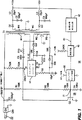
第1図は、発明的構成による制御回路を有する補助電源のブロック図である。
第2図は、発明的構成による制御回路を有する補助電源の慨略図であり、且つオン/オフ制御を詳細に示す。
第3図は、発明的構成による制御回路を有する補助電源の慨略図であり、且つ始動および故障検出回路を詳細に示す。
第4図は、発明的構成による電流過負荷検出回路を有する補助電源の慨略図である。
第5図は、発明的構成による高速リセット回路を有する補助電源の慨略図である。
発明の詳細な説明
第1図は全体として、発明的なスイッチ・モード電源10を示す。スイッチ・モード電源は、入力電圧(例えば、未調整B+電圧)からトランスT1の1次巻線W1に電流を供給してトランスT1の1つ以上の2次巻線W2、W3、W4、W5に電力を可変的に結合させるために周期的に動作できるスイッチング・コントローラU1を備えている。スイッチング・コントローラU1は、例えば、三洋電機(株)のSTK730シリーズのコントローラで構成できる。スイッチング・コントローラU1は、ピン4におけるその制御入力CNTLでドライブ電圧(例えば、未調整B+電圧)が得られると導通する。未調整B+入力供給電圧は、コンデンサC1で瀘波されるブリッジ整流器CR1の出力から得られる直流電圧である。未調整B+電圧は、スイッチ・モード電源10が家庭用のメイン(主電源)22に結合される(プラグを差し込まれる)といつでも存在する。しかしながら、電源10は実行モードでのみ動作し、静止モードすなわち待機モードでは動作不能とされる。
電源10がプラグを差し込まれ且つ実行モードにあるとき、未調整B+電圧はスイッチング・コントローラU1の制御入力CNTLに在るので、スイッチング・コントローラU1はトランスT1の1次巻線W1に電流を導通させることができる。巻線W1を流れる電流はトランスT1の巻線W2に電圧を誘起し、この電圧は抵抗R13とコンデンサC5を通って制御入力CNTLに印加される。巻線W2の極性は、巻線W2に誘起された電圧がスイッチング・コントローラU1を導通状態に保つような極性である。
スイッチング・コントローラU1で導かれる電流が抵抗R14とコンデンサC6の組合わせにより設定される制限閾値電流に達すると、スイッチング・コントローラU1は1次巻線を通って導通しなくなり、すなわち、オフになる。スイッチング・コントローラU1が導通しなくなると、1次巻線W1の磁界が崩壊し、その極性が逆転し、1次巻線W1の中にあるエネルギーは巻線W4とW5に移され、巻線W4とW5はそれぞれ、+15Vと−15Vの出力へ電力を供給する。
巻線W4とW5からのエネルギーが尽きると、これらの巻線の磁界が崩壊し、巻線の極性は逆転する。巻線W2とW4とW5の極性により、巻線W2はスイッチング・コントローラU1のピン4に正の電圧を供給し、それにより、スイッチング・コントローラU1は再び1次巻線W1に電流を導き、そして遂に、スイッチング・コントローラU1の電流制限閾値に達し、スイッチング・コントローラU1は電流を導かなくなる。それから再びエネルギーは1次巻線W1から巻線W4とW5に移される。このプロセスは、電源10の動作が安定するまで、数サイクル繰り返される。
電源10の動作が安定した後、帰還巻線W3はスイッチング・コントローラU1のデューティ・サイクルを制御する。帰還巻線W3に発生される電圧は、スイッチング・コントローラU1より発生される約−40.5Vの内部基準電圧と比較される。スイッチング・コントローラU1のデューティ・サイクルは、帰還巻線W3に発生される電圧がほぼ−40.5Vに維持されるように調整される。帰還巻線W3は2次巻線W4とW5に結合されるので、負荷の変動は帰還巻線W3に発生される電圧に反映される。従って帰還巻線W3は、巻線W4とW5で発生される出力電圧を調節するためにも使用される。
通常、待機モードから実行モードへまたは実行モードから待機モードへの切替えは、ユーザの制御下で、赤外線受信器、パネルスイッチなどのような制御入力(図示せず)を介して行なわれる。発明的特徴により、付加的な実行/待機スイッチング回路36が備えられ、電源10を、動作的な実行モードまたは非動作的な待機モードに切り替える。スイッチング・コントローラU1は大きな始動電流を必要とする。信頼できる始動を行ない且つこのドライブ電流の発生を助けるために、実行/待機スイッチング回路36は、未調整B+入力電圧と制御入力CNTL間に結合される第1の回路38を備え、未調整B+入力電圧が存在するときはいつも、スイッチング・コントローラによる導電を可能にするバイアス電圧を供給する。
発明的構成によれば、第1の回路38より供給されるこのドライブ・バイアス電流を分路にそらして、得られるドライブ電流を減らして、スイッチング・コントローラU1を動作不能にすることができる。ドライブ電流は基準電位源(例えば、大地)に分路することができる。
実行/待機スイッチング回路36は更に、トランスの2次巻線W4とW5のうち少なくとも1つに結合される故障状態検出回路42を含んでいる。検出回路42は、同じまたは別の2次巻線W4またはW5に結合される出力における低い閾値電圧を検出することにより、故障状態(例えば、補助電源にかかる過負荷電流)を検出する。故障状態検出回路42は故障状態を表示する出力41を発生してスイッチング・コントローラU1の導通を不能にするために、補助電源をオフにする手段として、あたかも装置(例えば、テレビジョン受像機)が待機動作モードに変更されたかのように、スイッチング・コントローラU1の制御入力CNTLを大地電位に引き込む。補助電源のセットアップ段階が、初期の低い電圧出力レベルのために、故障状態の誤った検出により妨げられないようにするために、遅延回路40は故障状態検出回路42の出力の効果を、補助電源の通常出力電圧レベルが確立されるのに十分な期間の間、阻止する。
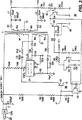
第2図〜第5図は、第1図に全体を示す発明的な構成についての異なる特徴を詳細に示す。すべての図面で、同一または同等の要素に関しては同じ参照番号が使用されている。第2図に関して述べると、スイッチング・コントローラU1はトランスT1の1次巻線W1と直列に結合される。スイッチング・コントローラU1は交互に導通しオフになり、電力を2次巻線に移送し、ここで生じるAC信号は、ダイオードD2とD3で整流され、コンデンサC2とC3でそれぞれ瀘波される。巻線W4とW5に発生される瀘波済みの電圧はそれぞれチョークL2とL3で更に瀘波され、動作電源電圧+15Vと−15Vをそれぞれ供給し、実行モードで負荷を起動する。2次巻線W4とW5の極性は、第2図に示すように、1次巻線W1の極性と反対であるので、スイッチング・コントローラU1がオフになり、トランスT1の1次巻線W1に貯えられたエネルギーが巻線W4とW5に移されるとコンデンサC2とC3は充電される。
発明的な特徴によれば、図に示す電源10は、スイッチング・コントローラU1の制御入力CNTLにおける電圧を更に制御して、実行モードと待機モードの切替えを制御するように構成される。装置が待機モードにあり且つスイッチング・コントローラU1が周期的に導通していないとき、電源10に入る唯一の電力は未調整B+電圧であり、装置が家庭のメイン22に結合されているので、未調整B+は存在している。実行/待機動作を制御する際、補足的な低電源(図示せず)から起動されるリレーまたは他のスイッチング・デバイスを使用して、未調整B+電圧を電源10のスイッチング要素へ結合させまたは減結合させることが可能である。このような解決手法は、未審査のドイツ特許庁出願DE 3607018A1に開示されている。しかしながら、本発明によれば、より一層費用効率の高い解決法を得るために、一部、未調整B+電圧から、そして一部、実行モード電圧から得られる信号を使用して、スイッチング・コントローラU1の制御入力CNTLにかかるバイアスを減らして、すなわち、制御入力にかかる電圧を大地電位に近づけて、通常のバイアスに回復するまでスイッチング・コントローラU1をオフに保つ。
従って、抵抗R1、R2、R3、R4から成る分圧器が、未調整B+電圧と大地間に結合され、分圧器の接合部J1は、コレクタが制御入力に結合されエミッタが接地されているスイッチング・トランジスタQ2のベースに結合される。未調整B+電圧が存在しているとき、制御入力CNTLはトランジスタQ2の導通により大地電位近くに引かれる。電源10は、メインに最初に結合されたとき、待機モードの状態に保持されている。
本発明は、コンバーゼンス増幅器のような実行モードの負荷を起動するために、補助電源(例えば、テレビジョンの補助電源)に有利に応用される。実行モードに切り替えるために、この発明的な電源はトランスT1の2次巻線以外の他のソースから発生される実行モードの電源電圧の存在を検出する。この実行モードの電源電圧は閾値レベルと比較され、閾値レベルを過ぎると、トランジスタQ2はオフにされ、スイッチング・コントローラU1の制御入力CNTLのバイアスを正常に戻し、且つ実行モードで、すなわち、トランスT1の帰還巻線W3による帰還制御下で、補助電源の動作を可能にする。例えば、テレビジョンの偏向回路その他の回路の実行モードの動作により発生される+23Vの電源電圧はこの目的に使用できる。
第2図で、ペアの差動PNPトランジスタQ3とQ4は、エミッタが抵抗R5によって実行モード電源電圧に結合され、トランジスタQ3のベースにある分圧器の抵抗R6とR7を介して、実行モードの電源電圧のレベルを、トランジスタQ4のベースのツェナダイオードZ3より供給される+8.2Vの基準電圧と比較する。実行モードの電源が分圧器内の抵抗の比率により定められるレベルを超えると、トランジスタQ4は導通し、オプトカプラU3をオンにスイッチする。オプトカプラU3のフォトトランジスタはトランジスタQ2のベースを接地させ、Q2は導通しなくなり、それによって、スイッチング・コントローラU1の制御入力CNTLに通常のバイアスがかけられる。次にトランスT1の2次巻線W2とW3にかかる電圧に応答し電源10の動作が実行モードで始まる。
別の発明的な実施例を第3図に示す。この中に含まれているラッチ回路は付加的な機能を有し、実行モードにあるとき、過負荷電流の状態を検出し、電源10を待機モードに切り替える。過負荷電流は出力電圧のレベルを通常値以下に低下させる。なぜなら、過電流の状態では、スイッチング・コントローラU1の過電流保護回路は、通常の出力電圧レベルを維持するのに十分な電力が電源10を通って結合されないうちに、スイッチング・コントローラU1をオフにしてまうからである。この電流制限方法は、投射型テレビジョンのディジタル・コンバーゼンス増幅器のような負荷を起動するのに決して最適とは言えない。このような負荷の場合、過電流の状態が生じたときに、低下した電圧で負荷に電流を供給しようとせずに、電源10をオフにすることができれば有利である。本発明によれば、この機能は、第2図のように、実行モードと待機モードの切替えを制御する回路とインタフェース(interface)する方法で達成される。
第3図で、待機モードから実行モードへ切り替えるための制御は、一部、+23Vの実行電源のような実行モードの電源電圧によって行なわれ、オプトカプラU3のLEDへ電流を供給する差動トランジスタ・ペアQ3とQ4によって決定される所定の電圧を通過させる。次に、オプトカプラU3のフォトトランジスタはトランジスタQ2をオフにし、スイッチング・コントローラU1の動作を可能にする。抵抗R1、R2、R3、R4は、未調整B+電源電圧から接続点J1においてトランジスタQ2にバイアスを供給する。第2図の実施例と比較すると、第2図では、オプトカプラU3内のLEDのカソードが接地されているが、第3図では、LEDを通る電流はPNPトランジスタQ5のベースを通ってコンデンサC4を充電する。
待機モードから実行モードへ最初に切り替えられるとコンデンサC4は遅延を与え、電源10は実行モードで始動することができる。電源10が作動しており、且つ調整された電圧(この場合、公称+15V)が+10Vを超えると、ツェナダイオードZ4は抵抗R8とR9を介して導通し、トランジスタQ6をオンにする。次に、オプトカプラU3からの電流はトランジスタQ6を通って大地に分路され、コンデンサC4は充電されなくなる。それで、トランジスタQ5はオフになり、コンデンサC4はトランジスタQ5を通って放電できず、またダイオードD6(+23Vの実行モード電源に結合され且つ逆バイアスされている)を通っても放電できない。
ツェナダイオードZ4を導通させるのに必要なレベル以下に+15Vの出力電圧が下がると、特に、2次巻線W4にかかる過負荷電流の場合、トランジスタQ6は、ベース・ドライブが不十分なために、オフになる。トランジスタQ6がオフになると、コンデンサC4はオプトカプラU3を通る電流から充電することができる。コンデンサC4の充電が約+10Vに達すると、トランジスタQ5はオフになり、オプトカプラU3を通る電流の通路はなくなる。その場合、作動トランジスタQ3とQ4は依然として+23Vの実行電源の存在を検出するが、オプトカプラU3のフォトトランジスタで導かれる電流はない。抵抗R1、R2、R3、R4により接合点J1に形成される分圧器のために、未調整B+電圧はトランジスタQ2をオンにする。スイッチング・コントローラU1の制御入力CNTLは低い状態(low)に引かれる。電源10は停止し、出力に結合される負荷を保護する。従って、電流を制限する方法では、スイッチング・コントローラの電流制限回路が出力電圧を通常値または公称値よりも低く下げて電力を供給し続けるのに対し、ここに述べる発明的な回路では、過電流の状態にある電源10をオフにスイッチする。これは、未調整B+電源から駆動される実行/待機回路を使用して行なわれ、最少限度の部品と複雑さで、過負荷電流保護機能が得られる。
第1図と第3図に示すように、故障状態検出回路42を使用して、電源10の+15V出力の電流過負荷状態が検出される。−15V出力の過負荷状態の検出は、正極性のみのバイアス電圧(例えば、未調整B+)が電源10に使用されるという事実によって難しくなる。
第4図に示す付加的な発明的構成では、負極性のバイアス電圧の不在の場合、−15V出力の電流過負荷状態の検出が有利に且つうまく行なわれる。実行モードにあるとき、−15V出力の電流過負荷状態が検出されると、電源10は待機モードに切り替えられる。第4図で、負の電源電圧過負荷検出回路43は、電源10の+15V出力と−15V出力との間に結合される。ツェナダイオードZ6は電源10の+15V出力と−15V出力との間でバイアスされ、−15V出力が正常に(normally)負荷されているとき、トランジスタQ3のベースは約−2Vのバイアス電圧を有する。従って、ツェナダイオードZ6は、レベルを変える機構(すなわち、dcオフセット)を提供し、−15Vの出力は正の基準電圧(この実施例では、トランジスタQ8のベース/エミッタ接合部のターン・オン電圧)と比較され、電流の過負荷状態を検出する。
もし、電流の過負荷状態に反応して、−15Vの出力が大地電位の方向へ下がり始めるならば、トランジスタQ8のベースにおける電圧も大地電位の方向へ移動する傾向がある。結局、もし電流過負荷状態が持続し、その結果、−15Vの出力が所定の閾値電圧レベルに達すると、トランジスタQ8のベースにおける電圧は正になり、結局、十分に高く(例えば、約0.7Vに)なり、トランジスタQ8をオンにし、電流過負荷状態を知らせる。故障状態検出回路42では電流過負荷状態はツェナダイオードZ4の導通状態の変化で知らされる。故障検出回路42とは異なり、電流過負荷状態がトランジスタQ8で知らされてもツェナダイオードZ6は導通状態のままになっている。ツェナダイオードZ6の破壊電圧を適正に選択することにより望ましい閾値レベルを選択することができる。
トランジスタQ8がオンになると、電流はトランジスタQ6のベースから引き出され、トランジスタQ6をオフにする。従って、+15V出力の過電流状態の検出と同様に、トランジスタQ6がオフになると、コンデンサC4はオプトカプラU3を通る電流から充電できる。コンデンサC4の充電が約+10Vに達すると、トランジスタQ5はオフになり、オプトカプラU3を通る電流路はなくなる。その場合、差動トランジスタQ3とQ4は依然として+23Vの実行電源の存在を検出するが、オプトカプラU3のフォトトランジスタで導かれる電流はない。接合点J1で抵抗R1、R2、R3、R4によって形成される分圧器のために、未調整B+電圧はトランジスタQ2をオンにする。スイッチング・コントローラU1の制御入力CNTLは低い状態に引かれる。電源10は停止し、出力に結合される負荷を保護する。
+23V実行電源電圧が下がると、コンデンサC4はダイオードD6(D6は+23V実行電源が存在すると逆バイアスされる)を通って放電する。コンデンサC4が放電を完了すると電源10は再始動できが、コンデンサC4の電荷がトランジスタQ5をオフにするのに十分な電圧にまで上昇できる遅延時間の間にトランジスタQ6をオンにするのに十分な出力電圧の発生を妨げる出力の過負荷状態がまだ存在する場合には再始動できない。
もしコンデンサC4が完全に放電するのに十分な時間を与えられなければ、例えば、もしスイッチ・モードの電源10が実行モードから待機モードへそして次に実行モードへと矢継ぎ早に切り替えられると、トランジスタQ6はオフのままである。従って、実行モードの出力電圧が現れて通常の出力電圧レベルに達するのを妨げられる。
第5図に示す更に別の発明的実施例は、+23Vの実行電源電圧が低下したときにコンデンサC4を素早く放電させるために高速リセット回路50を提供する。本発明によれば、この機能は、第2図のように、実行モードと待機モードの切替えを制御する回路とインタフェースする方法で達成される。
第5図で、遅延回路40はコンデンサC4と並列のツェナダイオードZ5を備える。+23Vの実行電源電圧が現れると、コンデンサC4は抵抗R10を介して充電され、実行モードの出力電圧がその通常の出力電圧レベルで安定するための遅延時間を与える。ツェナダイオードZ5はコンデンサC4の電圧を約+10Vにクランプし、ダーリントン構成に配列されるトランジスタQ8とQ9のベース・エミッタ接合部の損傷を防ぐ。
電源10が実行モードにあると、トランジスタQ4とオプトカプラU3のダイオードは、第3図の実施例と同様にして、電流を導く。しかしながら、この電流は、第3図の実施例と異なり、コンデンサC4を充電するのに使用されない。ダーリントン構成のトランジスタQ8とQ9は、トランジスタQ9のベースに最小限度のみの電流を生じる。従って、コンデンサC4の充電率およびそれによって生じる遅延時間はもっぱら、抵抗R10とコンデンサC4で形成される時定数で決定される。これによって、第3図のトランジスタQ5の電流増幅率(ベータ)あるいは第5図のトランジスタQ8と9のダーリントン構成によるコンデンサC4の充電率の変動が除去され有利である。
第5図に関して述べると、電源10が待機モードに切り替えられると、+23Vの実行電源電圧が低下し始める。実行電源電圧が、抵抗R6とR7から成る分圧器における抵抗比により定められるレベル以下に低下すると、電流の流れは再びトランジスタQ4からトランジスタQ3に向けられる。トランジスタQ3を通って流れる電流はある一定の電圧を抵抗R11に確立し、この電圧はリセット・トランジスタQ7をオンにバイアスする。そのためコンデンサC4は、+23Vの実行電圧が完全に衰退する以前に、抵抗R12とリセット・トランジスタQ7を介して素早く大地に放電する。 Industrial application fields
The present invention relates to the field of switched mode power supplies for devices (eg, television receivers) having a run mode of operation and a standby mode of operation. In particular, the present invention relates to the field of controlling an auxiliary power source when switching between an execution operation mode and a standby operation mode in such an apparatus.
Background of the Invention
A device capable of taking the so-called “standby” operating mode and the so-called “run” operating mode is described, for example, in US Pat. No. 5,017,844. As is known. For example, in a typical run / standby power supply used in a television receiver, when the power source is coupled to the main of the home, the bridge rectifier and filter capacitor are raw (raw: unregulated). DC voltage (B)+Voltage or unadjusted B+Supply voltage). The standby mode load is directly B+It can be started from a voltage or from another voltage that is always present. However, many execution mode loads are activated through a voltage regulated power supply (eg, a switch mode power supply) that operates only in the execution mode. Run-mode power supplies for certain types of loads (eg, deflection circuits, high voltage screen loads) typically use flyback transformers that produce beam deflection. A separate or auxiliary power supply can also be used as a switch mode power supply, and a regulated B for a flyback transformer+Supply voltage, and other auxiliary power supply voltages.
For example, projection televisions are equipped with three high power cathode ray tubes (CRTs), so the need for power is particularly severe. In general, an auxiliary power source is useful to activate these CRT convergence amplifiers (two such amplifiers are required for each CRT). These amplifiers require positive and negative voltages and consume a considerable amount of power.
In a switch mode power supply, the input DC voltage (eg, B in a television receiver)+Voltage) is coupled to one terminal of the primary winding of the transformer, the other terminal of the primary winding is coupled to the switching device, and when the switching device is conducting, the current is coupled to the transformer. The switching device is alternately turned on and off during the run mode of operation to provide alternating current to the transformer secondary winding, which is rectified and rippled to provide the run mode power supply voltage.
The adjustment of the output voltage is performed by feedback control supplied from a feedback winding of the transformer, for example. Each secondary winding is intimately coupled, and load variations associated with the secondary winding are reflected in the feedback winding. The feedback control compares the standard voltage or threshold voltage level supplied from the switching device with the voltage applied to the feedback winding, and modulates the frequency and / or pulse width when the switching circuit is turned on / off. Switching device is unadjusted B+The input voltage is corrected so as not to be felt, and an accurate output voltage level is maintained as the current load fluctuates within a normal power consumption range.
An STK730 series integrated circuit (IC) power supply controller manufactured by Sanyo Electric Co., Ltd. can be used as a switching device for power supply as described above. The controller includes a FET power switching transistor, an error amplifier / driver, and an overcurrent protection circuit in a single package. When coupled to a switch mode power supply and first turned on, B+Current from the voltage flows to ground through the transformer primary winding, FET and current sensing resistor. The current continues to increase until the overcurrent protection circuit in the controller IC is started, and then the IC controller turns off its FET power transistor. The energy is transferred to the secondary winding of the transformer, where the induced current is rectified and charges the filter capacitor. After a start-up period consisting of several cycles, the output voltage reaches its regulated level. A threshold comparison circuit provided by the IC controller is coupled to the feedback winding of the transformer and controls the switching timing by the control IC to maintain the regulated output voltage level. Oscillation is stable at a frequency and duty cycle that accommodates the load coupled to the secondary winding. Many other power controllers operate similarly and can be used in place of the Sanyo Electric STK730 series.
Such an IC controller is not adjusted B+Always try to start when voltage is present. Another switch circuit controls switching between the standby mode and the execution mode.
The FET power transistor in an IC controller such as the STK-730 series is partly coupled to a voltage or current signal generated in the primary winding by the operation of the switching circuit, and advantageously the switching transistor is: It is driven stronger as the current increases in the primary winding. In order for a switching transistor to begin to conduct, it requires a positive voltage at its gate drive input, and if the control voltage is too low, it will not reliably conduct or be switched off. One way to prevent the operation of the switching transistor is to provide a means for reducing the voltage at the control input. This seems to be one way to switch power on / off or run / standby mode. However, unadjusted B+The voltage exists in both run mode and standby mode (if the auxiliary power source is coupled to the home main) and unregulated B+The voltage is the only voltage that exists during standby.
Summary of the Invention
This unadjusted B+It is advantageous to control the switching between the standby mode and the execution mode of the auxiliary power supply using the voltage. In addition, in order to avoid interference from the failure detection circuit that hinders the completion of the start-up stage of the auxiliary power supply, the switching between the standby mode and the execution mode of the auxiliary power supply is controlled, and only the current control circuit of the power supply IC controller during startup It would be advantageous to be able to control the auxiliary power supply.
The switch mode power supply circuit according to the inventive configuration is not adjusted B+A voltage is supplied from the input voltage to the control input of the controller IC to control the operation of the power supply controller IC, bias the switching transistor, and lower the voltage at the input of the controller IC to disable the controller IC. When the run mode voltage is detected and the power supply is started by changing the state of the switching transistor, the power supply operates in dependence on the current control circuit of the controller IC during the start-up phase.
The switch controller is adapted to respond to fault condition detectors such as undervoltage and / or overcurrent detectors, each of which indicates a fault condition such as a short circuit. However, the low voltage level generated during start-up can be mistaken for a fault condition. Therefore, a delay circuit can be arranged between the failure state detector and the switch control device. For a period of time after the auxiliary power is turned on, the fault condition detector prevents the auxiliary power from becoming inoperable, giving the auxiliary power the opportunity to establish an operating output voltage without being mistaken for a fault condition.
An auxiliary power supply in a device having an execution mode of operation and a standby mode of operation according to an inventive configuration consists of: a voltage source, a transformer and a switching unit coupled to generate an output supply voltage in switch mode A feedback circuit for initiating conduction of the switching controller; and switching for switching the auxiliary power supply between an operating mode and a non-operating mode in response to an on / off signal indicating an execution operation mode and a standby operation mode of the device. circuit. The switching circuit is energized by the voltage source and blocks the feedback circuit to block the operation of the switching controller during a standby mode of operation of the device.
In the preferred embodiment, the voltage source is an unregulated rectified mains voltage source, and the on / off signal is supplied from another device in the device powered by the unregulated rectified main voltage source. This is the power supply voltage of the execution mode generated by the power supply. The feedback circuit generates a feedback signal, and the switching circuit shunts the feedback signal to a reference voltage source.
According to another inventive configuration, an auxiliary power source for a device having an active mode of operation and a standby mode of operation comprises: a primary winding coupled to a voltage source and at least one secondary winding Transformer; a switching controller coupled to the primary winding and operable to allow conduction of current through the primary winding: power is supplied to the at least one two by the periodic conduction of the switching controller A feedback controller coupled to the at least one secondary winding and the switching controller: the feedback controller generates a feedback signal and enables periodic conduction of the switching controller; And an operation mode of the auxiliary power supply in response to an on / off signal indicating an execution operation mode and a standby operation mode of the apparatus; The switching circuit switches the operating mode: the switching circuit by preventing the feedback controller, so as to prevent the switching controller for operation during the standby mode of operation of the device.
In a preferred embodiment, the switching control circuit comprises: a voltage divider coupled to the voltage source; energized by the voltage divider and coupled to the switching controller to shunt the feedback signal A first transistor that shuts off the feedback controller by: a voltage threshold detector responsive to a power supply voltage in an execution mode generated by another power source in the device; and optically coupled to the voltage threshold detector; A second transistor that controls conduction of the first transistor. This voltage source is an unregulated DC voltage that is rectified from the main AC power source.
According to yet another inventive configuration, the configuration of the power supply for a device having an active mode of operation and a standby mode of operation consists of the following: powered by a rectified main voltage source and operating in switch mode And a main power supply that generates at least one run mode power supply voltage; energized by the rectified main voltage source, operates in switch mode, and generates at least one run mode power supply voltage in response to a feedback signal. A control circuit that switches the auxiliary power supply between an operating mode and a non-operating mode in response to an on / off signal that indicates an execution operation mode and a standby operation mode of the apparatus; The switching circuit blocks the feedback signal so as to block the operation of the auxiliary power source during the standby mode of operation of the device.
In a preferred embodiment, the control circuit comprises the following: a voltage divider coupled to the rectified main voltage source; a voltage divider energized by the voltage divider and coupled to shunt the feedback signal. A voltage threshold detector responsive to the at least one run mode power supply voltage; and a second transistor optically coupled to the voltage threshold detector to control conduction of the first transistor.
Correspondence between the claims and the embodiments is indicated by reference numerals used in the drawings as follows.
1. An auxiliary power supply in a device having an execution operation mode and a standby operation mode,
A voltage source (unregulated B) coupled to generate the output supply voltage in switch mode+), Transformer (T1) and switching controller;
A feedback circuit (W2) coupled to the control input of the switching controller to maintain operation of the switching controller;
Switching circuits (R1, R2, R3,...) That switch the auxiliary power supply between an operation mode and a non-operation mode in response to an on / off signal (+ 23V-execution) indicating the execution operation mode and the standby operation mode of the device. R4, Q2, 16)
The switching circuit is energized by the voltage source and blocks the feedback circuit by changing a bias voltage at the control input to block the switching controller during the standby mode of operation of the device. The auxiliary power source.
2. The auxiliary power supply according to claim 1, wherein the on / off signal (+ 23V-execution) is an execution mode voltage generated by another power supply in the apparatus.
3. The voltage source (unadjusted B+The auxiliary power supply of claim 1, wherein) is an unregulated rectified main voltage source.
4). The voltage source (B+) Is an unregulated rectified main voltage source, and the on / off signal (+ 23V-execution) is activated by the unregulated rectified main voltage source The auxiliary power supply according to claim 1, wherein the power supply voltage is an execution mode power supply voltage generated by the power supply.
5. The auxiliary circuit according to claim 1, wherein the feedback circuit (W2) generates a feedback signal and the switching circuit (R1, R2, R3, R4, Q2, 16) shunts the feedback signal to a reference voltage source. Power supply.
[Brief description of the drawings]
FIG. 1 is a block diagram of an auxiliary power source having a control circuit according to an inventive configuration.
FIG. 2 is a schematic diagram of an auxiliary power source having a control circuit according to an inventive configuration, and shows in detail on / off control.
FIG. 3 is a schematic diagram of an auxiliary power supply having a control circuit according to an inventive configuration and shows in detail the start-up and fault detection circuit.
FIG. 4 is a schematic diagram of an auxiliary power supply having a current overload detection circuit according to an inventive configuration.
FIG. 5 is a schematic diagram of an auxiliary power supply having a fast reset circuit according to an inventive configuration.
Detailed Description of the Invention
FIG. 1 generally shows an inventive switch mode power supply 10. The switch mode power supply is connected to the input voltage (eg, unregulated B+Voltage) to provide a current to the primary winding W1 of the transformer T1 to variably couple power to one or more secondary windings W2, W3, W4, W5 of the transformer T1. A switching controller U1 is provided. The switching controller U1 can be configured by, for example, an STK730 series controller from Sanyo Electric Co., Ltd. The switching controller U1 is driven by its control input CNTL at pin 4 (eg unadjusted B+When voltage is obtained, it becomes conductive. Unadjusted B+The input supply voltage is a DC voltage obtained from the output of the bridge rectifier CR1 that is rippled by the capacitor C1. Unadjusted B+The voltage is present whenever the switch mode power supply 10 is coupled (plugged in) to the home main (main power) 22. However, the power supply 10 operates only in the execution mode and is disabled in the stationary mode, that is, the standby mode.
When power supply 10 is plugged in and in run mode, unadjusted B+Since the voltage is at the control input CNTL of the switching controller U1, the switching controller U1 can conduct current to the primary winding W1 of the transformer T1. The current flowing through the winding W1 induces a voltage in the winding W2 of the transformer T1, and this voltage is applied to the control input CNTL through the resistor R13 and the capacitor C5. The polarity of the winding W2 is such that the voltage induced in the winding W2 keeps the switching controller U1 conductive.
When the current drawn by the switching controller U1 reaches a limit threshold current set by the combination of the resistor R14 and the capacitor C6, the switching controller U1 does not conduct through the primary winding, i.e. turns off. When the switching controller U1 stops conducting, the magnetic field of the primary winding W1 collapses, its polarity reverses, energy in the primary winding W1 is transferred to the windings W4 and W5, and the winding W4 And W5 supply power to the + 15V and -15V outputs, respectively.
When the energy from the windings W4 and W5 is exhausted, the magnetic fields of these windings collapse and the polarity of the windings is reversed. Due to the polarity of windings W2, W4 and W5, winding W2 supplies a positive voltage to pin 4 of switching controller U1, so that switching controller U1 again conducts current to primary winding W1, and Eventually, the current limit threshold of switching controller U1 is reached and switching controller U1 no longer conducts current. Then again the energy is transferred from the primary winding W1 to windings W4 and W5. This process is repeated for several cycles until the operation of the power supply 10 is stabilized.
After the operation of the power supply 10 is stabilized, the feedback winding W3 controls the duty cycle of the switching controller U1. The voltage generated in the feedback winding W3 is compared with an internal reference voltage of about -40.5V generated from the switching controller U1. The duty cycle of the switching controller U1 is adjusted so that the voltage generated in the feedback winding W3 is maintained at approximately -40.5V. Since the feedback winding W3 is coupled to the secondary windings W4 and W5, the load variation is reflected in the voltage generated in the feedback winding W3. Therefore, the feedback winding W3 is also used to adjust the output voltage generated by the windings W4 and W5.
Normally, switching from the standby mode to the execution mode or from the execution mode to the standby mode is performed via a control input (not shown) such as an infrared receiver or a panel switch under the control of the user. In accordance with inventive features, an additional run /
According to the inventive configuration, this drive bias current supplied from the
The run /
FIGS. 2-5 show in detail the different features of the inventive configuration generally shown in FIG. The same reference numbers are used for the same or equivalent elements in all drawings. Referring to FIG. 2, switching controller U1 is coupled in series with primary winding W1 of transformer T1. The switching controller U1 is alternately turned on and off, transferring power to the secondary winding, and the resulting AC signal is rectified by diodes D2 and D3 and is sunk by capacitors C2 and C3, respectively. The rippled voltages generated in the windings W4 and W5 are further rippled by the chokes L2 and L3, respectively, and supply the operating power supply voltages + 15V and -15V, respectively, to start the load in the execution mode. As shown in FIG. 2, the polarity of the secondary windings W4 and W5 is opposite to the polarity of the primary winding W1, so the switching controller U1 is turned off and the primary winding W1 of the transformer T1 is turned off. When the stored energy is transferred to windings W4 and W5, capacitors C2 and C3 are charged.
According to an inventive feature, the power supply 10 shown in the figure is configured to further control the voltage at the control input CNTL of the switching controller U1 to control switching between the execution mode and the standby mode. When the device is in standby mode and switching controller U1 is not periodically conducting, the only power entering power supply 10 is unregulated B+Voltage, and the device is coupled to the home main 22 so unadjusted B+Is present. When controlling run / standby operation, using a relay or other switching device activated from a supplemental low power supply (not shown)+The voltage can be coupled or decoupled to the switching element of the power supply 10. Such a solution is disclosed in the unexamined German Patent Office application DE 3607018 A1. However, according to the present invention, in order to obtain a more cost-effective solution, some unadjusted B+Using the signal derived from the voltage and partly from the run mode voltage, the bias applied to the control input CNTL of the switching controller U1 is reduced, ie, the voltage applied to the control input is brought close to the ground potential, The switching controller U1 is kept off until the bias is restored.
Therefore, the voltage divider consisting of resistors R1, R2, R3, R4 is not adjusted B+Coupled between voltage and ground, the voltage divider junction J1 is coupled to the base of a switching transistor Q2 whose collector is coupled to the control input and whose emitter is grounded. Unadjusted B+When voltage is present, the control input CNTL is pulled close to ground potential by the conduction of transistor Q2. The power supply 10 is held in a standby mode when it is first coupled to the main.
The present invention is advantageously applied to an auxiliary power source (e.g., an auxiliary power source for a television) for activating a load of an execution mode such as a convergence amplifier. In order to switch to the run mode, the inventive power supply detects the presence of a run mode power supply voltage generated from a source other than the secondary winding of the transformer T1. The power supply voltage in this execution mode is compared with the threshold level, after which the transistor Q2 is turned off, the bias of the control input CNTL of the switching controller U1 is returned to normal, and in the execution mode, ie the transformer T1 The auxiliary power supply can be operated under feedback control by the feedback winding W3. For example, a + 23V supply voltage generated by the operation of the television deflection circuit and other circuits in the execution mode can be used for this purpose.
In FIG. 2, the pair of differential PNP transistors Q3 and Q4 have their emitters coupled to the run mode power supply voltage by resistor R5 and run through the voltage divider resistors R6 and R7 at the base of transistor Q3. The voltage level is compared with a +8.2 V reference voltage supplied from a Zener diode Z3 at the base of transistor Q4. When the run mode power supply exceeds a level determined by the ratio of the resistors in the voltage divider, transistor Q4 conducts and switches on optocoupler U3. The phototransistor of optocoupler U3 grounds the base of transistor Q2, which causes Q2 to become nonconductive, thereby normally biasing the control input CNTL of switching controller U1. Next, the operation of the power supply 10 starts in the execution mode in response to the voltage applied to the secondary windings W2 and W3 of the transformer T1.
Another inventive embodiment is shown in FIG. The latch circuit included therein has an additional function. When in the execution mode, the latch circuit detects an overload current state and switches the power supply 10 to the standby mode. Overload current reduces the output voltage level below normal. Because in an overcurrent condition, the overcurrent protection circuit of switching controller U1 turns off switching controller U1 before enough power is coupled through power supply 10 to maintain a normal output voltage level. It is because it will wait. This current limiting method is by no means optimal for starting a load such as a projection television digital convergence amplifier. In the case of such a load, it is advantageous if the power supply 10 can be turned off when an overcurrent condition occurs without attempting to supply current to the load with a reduced voltage. According to the present invention, this function is achieved by a method of interfacing with a circuit that controls switching between the execution mode and the standby mode, as shown in FIG.
In FIG. 3, the control for switching from the standby mode to the execution mode is partly performed by the power supply voltage of the execution mode such as the execution power supply of + 23V, and a differential transistor pair for supplying current to the LED of the optocoupler U3. A predetermined voltage determined by Q3 and Q4 is passed. Next, the phototransistor of optocoupler U3 turns off transistor Q2 and enables operation of switching controller U1. Resistors R1, R2, R3, R4 are unadjusted B+A bias is supplied from the power supply voltage to the transistor Q2 at the connection point J1. Compared with the embodiment of FIG. 2, in FIG. 2, the cathode of the LED in the optocoupler U3 is grounded, but in FIG. 3, the current through the LED passes through the base of the PNP transistor Q5 to the capacitor C4. Charge.
When initially switched from standby mode to run mode, capacitor C4 provides a delay and power supply 10 can be started in run mode. When power supply 10 is operating and the regulated voltage (in this case nominally + 15V) exceeds + 10V, Zener diode Z4 conducts through resistors R8 and R9 and turns on transistor Q6. Next, the current from optocoupler U3 is shunted to ground through transistor Q6 and capacitor C4 is no longer charged. Thus, transistor Q5 turns off and capacitor C4 cannot discharge through transistor Q5, nor can it discharge through diode D6 (coupled to the + 23V run mode power supply and reverse biased).
When the output voltage of + 15V drops below the level required to turn on the Zener diode Z4, especially in the case of an overload current applied to the secondary winding W4, the transistor Q6 has insufficient base drive. Turn off. When transistor Q6 is turned off, capacitor C4 can be charged from the current through optocoupler U3. When the charge on capacitor C4 reaches approximately + 10V, transistor Q5 turns off and there is no current path through optocoupler U3. In that case, the actuating transistors Q3 and Q4 still detect the presence of the + 23V running power supply, but there is no current drawn by the optocoupler U3 phototransistor. Because of the voltage divider formed at junction J1 by resistors R1, R2, R3, R4, unadjusted B+The voltage turns on transistor Q2. The control input CNTL of the switching controller U1 is pulled low. The power supply 10 stops and protects the load coupled to the output. Thus, in the current limiting method, the switching controller's current limiting circuit continues to deliver power with the output voltage lower than normal or nominal, whereas in the inventive circuit described herein, the overcurrent The power supply 10 in the state is switched off. This is unadjusted B+This is done using a run / standby circuit driven from a power source, and with the minimum number of components and complexity, an overload current protection function is obtained.
As shown in FIG. 1 and FIG. 3, a fault
In the additional inventive configuration shown in FIG. 4, in the absence of a negative bias voltage, the detection of a current overload condition of -15 V output is advantageously and successfully performed. When in the execution mode, when a current overload state of -15V output is detected, the power supply 10 is switched to the standby mode. In FIG. 4, the negative power supply voltage
If the -15V output begins to drop in the direction of ground potential in response to a current overload condition, the voltage at the base of transistor Q8 also tends to move in the direction of ground potential. Eventually, if the current overload condition persists so that the -15V output reaches a predetermined threshold voltage level, the voltage at the base of transistor Q8 will be positive and eventually high enough (eg, about 0. 0. 7V), turns on transistor Q8 to signal a current overload condition. In the failure
When transistor Q8 is turned on, current is drawn from the base of transistor Q6, turning transistor Q6 off. Therefore, similar to the detection of the + 15V output overcurrent condition, when transistor Q6 is turned off, capacitor C4 can be charged from the current through optocoupler U3. When the charging of the capacitor C4 reaches about + 10V, the transistor Q5 is turned off and there is no current path through the optocoupler U3. In that case, differential transistors Q3 and Q4 still detect the presence of the + 23V execution power supply, but there is no current drawn by the phototransistor of optocoupler U3. Because of the voltage divider formed by resistors R1, R2, R3, R4 at junction J1, unadjusted B+The voltage turns on transistor Q2. The control input CNTL of the switching controller U1 is pulled low. The power supply 10 stops and protects the load coupled to the output.
When the + 23V execution power supply voltage drops, capacitor C4 discharges through diode D6 (D6 is reverse biased when + 23V execution power supply is present). When capacitor C4 completes discharging, power supply 10 can be restarted, but sufficient to turn on transistor Q6 during a delay time that allows the charge on capacitor C4 to rise to a voltage sufficient to turn off transistor Q5. If there is still an output overload condition that prevents the output voltage from occurring, it cannot be restarted.
If sufficient time is not allowed for the capacitor C4 to fully discharge, for example, if the switch mode power supply 10 is rapidly switched from run mode to standby mode and then to run mode, transistor Q6 Remains off. Therefore, the output voltage of the execution mode appears and is prevented from reaching the normal output voltage level.
Yet another inventive embodiment shown in FIG. 5 provides a
In FIG. 5, the
When the power supply 10 is in the execution mode, the transistor Q4 and the diode of the optocoupler U3 conduct current in the same manner as in the embodiment of FIG. However, this current is not used to charge capacitor C4, unlike the embodiment of FIG. Transistors Q8 and Q9 in the Darlington configuration produce only a minimum current at the base of transistor Q9. Therefore, the charging rate of the capacitor C4 and the delay time caused thereby are determined solely by the time constant formed by the resistor R10 and the capacitor C4. This advantageously eliminates fluctuations in the charging rate of the capacitor C4 due to the current amplification factor (beta) of the transistor Q5 in FIG. 3 or the Darlington configuration of the transistors Q8 and 9 in FIG.
Referring to FIG. 5, when the power supply 10 is switched to the standby mode, the execution power supply voltage of + 23V starts to decrease. When the running power supply voltage drops below a level determined by the resistance ratio in the voltage divider consisting of resistors R6 and R7, the current flow is again directed from transistor Q4 to transistor Q3. The current flowing through transistor Q3 establishes a certain voltage across resistor R11, which biases reset transistor Q7 on. Capacitor C4 thus quickly discharges to ground through resistor R12 and reset transistor Q7 before the + 23V running voltage has completely decayed.
Claims (5)
出力供給電圧をスイッチ・モードで発生させるために結合される、電圧源、トランスおよびスイッチング・コントローラと、
前記スイッチング・コントローラの動作を維持するために前記スイッチング・コントローラの制御入力に結合される、帰還回路と、
前記装置の実行動作モードと待機動作モードを表示するオン/オフ信号に応答して前記補助電源を動作モードと非動作モードの間で切り替える、スイッチング回路と、を有し、
前記スイッチング回路は、前記電圧源で付勢され、前記装置の待機動作モードの間に前記スイッチング・コントローラを阻止するために、前記制御入力においてバイアス電圧を変化させるようにして前記帰還回路を阻止する、前記補助電源。An auxiliary power supply in a device having an execution operation mode and a standby operation mode,
A voltage source, a transformer and a switching controller coupled to generate an output supply voltage in switch mode;
A feedback circuit coupled to the control input of the switching controller to maintain operation of the switching controller ;
A switching circuit that switches the auxiliary power supply between an operation mode and a non-operation mode in response to an on / off signal that displays an execution operation mode and a standby operation mode of the device ;
The switching circuit is energized by the voltage source and blocks the feedback circuit by changing a bias voltage at the control input to block the switching controller during the standby mode of operation of the device. The auxiliary power source.
Applications Claiming Priority (3)
| Application Number | Priority Date | Filing Date | Title |
|---|---|---|---|
| US08/749,750 | 1996-11-15 | ||
| US08/749,750 US5949154A (en) | 1996-11-15 | 1996-11-15 | Auxiliary power supply control |
| PCT/US1997/021008 WO1998021813A1 (en) | 1996-11-15 | 1997-11-12 | Auxiliary power supply control |
Publications (3)
| Publication Number | Publication Date |
|---|---|
| JP2001503957A JP2001503957A (en) | 2001-03-21 |
| JP2001503957A5 JP2001503957A5 (en) | 2005-07-14 |
| JP3880071B2 true JP3880071B2 (en) | 2007-02-14 |
Family
ID=25015028
Family Applications (1)
| Application Number | Title | Priority Date | Filing Date |
|---|---|---|---|
| JP52290198A Expired - Fee Related JP3880071B2 (en) | 1996-11-15 | 1997-11-12 | Power supply |
Country Status (10)
| Country | Link |
|---|---|
| US (1) | US5949154A (en) |
| EP (1) | EP0938771B1 (en) |
| JP (1) | JP3880071B2 (en) |
| KR (1) | KR100521112B1 (en) |
| CN (1) | CN1076537C (en) |
| AU (1) | AU5442398A (en) |
| DE (1) | DE69719207T2 (en) |
| ES (1) | ES2191865T3 (en) |
| MY (1) | MY118078A (en) |
| WO (1) | WO1998021813A1 (en) |
Families Citing this family (21)
| Publication number | Priority date | Publication date | Assignee | Title |
|---|---|---|---|---|
| EP0991170B1 (en) * | 1998-09-28 | 2003-11-26 | STMicroelectronics S.r.l. | Integrated protection from the effects of a short circuit of the output of a flyback converter |
| US6337788B1 (en) | 1998-11-16 | 2002-01-08 | Power Integrations, Inc. | Fault condition protection |
| CA2385145A1 (en) * | 1999-10-01 | 2001-04-12 | Online Power Supply, Inc. | Non-saturating magnetic element(s) power converters and surge protection |
| US6272025B1 (en) | 1999-10-01 | 2001-08-07 | Online Power Supply, Inc. | Individual for distributed non-saturated magnetic element(s) (referenced herein as NSME) power converters |
| US6157549A (en) * | 1999-10-22 | 2000-12-05 | Thomson Licensing S.A. | Power supply with multiple mode operation |
| EP1209793A1 (en) * | 2000-11-23 | 2002-05-29 | Semiconductor Components Industries LLC | Apparatus and method for controlling a power supply |
| US6580593B2 (en) * | 2001-03-14 | 2003-06-17 | Power Integrations, Inc. | Method and apparatus for fault condition protection of a switched mode power supply |
| JP2003018828A (en) * | 2001-06-28 | 2003-01-17 | Sanken Electric Co Ltd | Dc-dc converter |
| US6952355B2 (en) * | 2002-07-22 | 2005-10-04 | Ops Power Llc | Two-stage converter using low permeability magnetics |
| KR100586988B1 (en) * | 2004-08-09 | 2006-06-08 | 삼성전자주식회사 | electronic device |
| ATE383734T1 (en) * | 2005-03-09 | 2008-01-15 | Patent Treuhand Ges Fuer Elektrische Gluehlampen Mbh | OVERLOAD PROTECTION DEVICE FOR ELECTRONIC CONVERTERS, FOR EXAMPLE FOR HALOGEN LAMPS |
| US8077483B2 (en) | 2007-04-06 | 2011-12-13 | Power Integrations, Inc. | Method and apparatus for sensing multiple voltage values from a single terminal of a power converter controller |
| DE112009001370T5 (en) * | 2008-05-27 | 2011-04-28 | ASIC Advantage, Inc., Sunnyvale | Power supply with standby power |
| FR2960661B1 (en) * | 2010-05-27 | 2013-04-05 | Sagemcom Broadband Sas | DEVICE FOR AUXILIARY POWERING OF EQUIPMENT ON A CURRENT POWER SUPPLY BUS |
| WO2012100406A1 (en) * | 2011-01-24 | 2012-08-02 | 深圳矽睿芯科技有限公司 | Power supply circuit with low-voltage control and producing method thereof |
| KR101232917B1 (en) | 2011-09-28 | 2013-02-13 | 오텍캐리어 주식회사 | Method for controlling standby power of airconditioner |
| KR101709484B1 (en) * | 2011-12-14 | 2017-02-24 | 주식회사 솔루엠 | Power supplying apparatus |
| US9368269B2 (en) * | 2012-10-24 | 2016-06-14 | Schumacher Electric Corporation | Hybrid battery charger |
| CN104052253B (en) * | 2013-03-12 | 2016-12-28 | 力博特公司 | Power on-off control circuit |
| US10136500B2 (en) | 2015-03-30 | 2018-11-20 | Philips Lighting Holding B.V. | Isolated driver |
| DE102017111431A1 (en) | 2017-05-24 | 2018-11-29 | Endress+Hauser SE+Co. KG | Primary switched switching network |
Family Cites Families (8)
| Publication number | Priority date | Publication date | Assignee | Title |
|---|---|---|---|---|
| DE3341074A1 (en) * | 1983-11-12 | 1985-05-23 | Telefunken Fernseh Und Rundfunk Gmbh, 3000 Hannover | SWITCHING POWER SUPPLY, ESPECIALLY FOR A TELEVISION RECEIVER, WITH A PROTECTIVE CIRCUIT TO LIMIT THE PRIMARY CURRENT |
| DE3607018A1 (en) * | 1986-03-04 | 1987-09-10 | Siemens Ag | Switched-mode power supply |
| FR2607991B1 (en) * | 1986-12-05 | 1989-02-03 | Radiotechnique Ind & Comm | CUT-OUT POWER SUPPLY FOR A TELEVISION EQUIPPED WITH A STAND-BY SYSTEM |
| US4941078A (en) * | 1989-03-07 | 1990-07-10 | Rca Licensing Corporation | Synchronized switch-mode power supply |
| US5017844A (en) * | 1990-04-30 | 1991-05-21 | Rca Licensing Corporation | Disabling arrangement for a circuit operating at a deflection rate |
| GB9114354D0 (en) * | 1991-07-03 | 1991-08-21 | Thompson Consumer Electronics | Run/standby control with switched mode power supply |
| GB2283135A (en) * | 1993-10-20 | 1995-04-26 | Thomson Consumer Electronics | Switch mode power supply circuit |
| JPH07308065A (en) * | 1994-05-10 | 1995-11-21 | Ricoh Co Ltd | Power supply |
-
1996
- 1996-11-15 US US08/749,750 patent/US5949154A/en not_active Expired - Fee Related
-
1997
- 1997-11-12 WO PCT/US1997/021008 patent/WO1998021813A1/en active IP Right Grant
- 1997-11-12 JP JP52290198A patent/JP3880071B2/en not_active Expired - Fee Related
- 1997-11-12 CN CN97199704A patent/CN1076537C/en not_active Expired - Fee Related
- 1997-11-12 AU AU54423/98A patent/AU5442398A/en not_active Abandoned
- 1997-11-12 EP EP97948337A patent/EP0938771B1/en not_active Expired - Lifetime
- 1997-11-12 ES ES97948337T patent/ES2191865T3/en not_active Expired - Lifetime
- 1997-11-12 KR KR10-1999-7004243A patent/KR100521112B1/en not_active IP Right Cessation
- 1997-11-12 DE DE1997619207 patent/DE69719207T2/en not_active Expired - Lifetime
- 1997-11-14 MY MYPI97005462A patent/MY118078A/en unknown
Also Published As
| Publication number | Publication date |
|---|---|
| US5949154A (en) | 1999-09-07 |
| CN1076537C (en) | 2001-12-19 |
| MY118078A (en) | 2004-08-30 |
| EP0938771B1 (en) | 2003-02-19 |
| ES2191865T3 (en) | 2003-09-16 |
| WO1998021813A1 (en) | 1998-05-22 |
| EP0938771A1 (en) | 1999-09-01 |
| AU5442398A (en) | 1998-06-03 |
| DE69719207D1 (en) | 2003-03-27 |
| KR100521112B1 (en) | 2005-10-14 |
| JP2001503957A (en) | 2001-03-21 |
| DE69719207T2 (en) | 2004-02-12 |
| KR20000053264A (en) | 2000-08-25 |
| CN1238072A (en) | 1999-12-08 |
Similar Documents
| Publication | Publication Date | Title |
|---|---|---|
| JP3784838B2 (en) | Switch power supply | |
| JP3880071B2 (en) | Power supply | |
| KR100465577B1 (en) | Quick-reset circuit for auxiliary power supply | |
| KR100522017B1 (en) | Fault control circuit for switched power supply | |
| US6385060B1 (en) | Switching power supply with reduced energy transfer during a fault condition | |
| US4516168A (en) | Shutdown circuit for a switching regulator in a remote controlled television receiver | |
| JPH0624390U (en) | Power supply circuit | |
| US5017844A (en) | Disabling arrangement for a circuit operating at a deflection rate | |
| JP2002204572A (en) | Switching power and control method for the same | |
| US4234829A (en) | High voltage disabling circuit for a television receiver | |
| JPH0795434A (en) | Voltage stabilizer | |
| JP2869755B2 (en) | Power supply and horizontal deflection system | |
| EP0650294B1 (en) | Switch mode power supply circuit | |
| US4755923A (en) | Regulated high-voltage power supply | |
| JP4332935B2 (en) | Television receiver | |
| MXPA99004385A (en) | Quick-reset circuit for auxiliary power supply | |
| MXPA99004384A (en) | Fault control circuit for switched power supply | |
| MXPA99004386A (en) | Auxiliary power supply control | |
| MXPA99004387A (en) | Fault control circuit for switched power supply | |
| JPH08294274A (en) | Switching power unit | |
| JPH0731139A (en) | Dc converter | |
| JPH11266581A (en) | Power source |
Legal Events
| Date | Code | Title | Description |
|---|---|---|---|
| A521 | Written amendment |
Free format text: JAPANESE INTERMEDIATE CODE: A523 Effective date: 20041102 |
|
| A621 | Written request for application examination |
Free format text: JAPANESE INTERMEDIATE CODE: A621 Effective date: 20041102 |
|
| A131 | Notification of reasons for refusal |
Free format text: JAPANESE INTERMEDIATE CODE: A131 Effective date: 20060314 |
|
| A601 | Written request for extension of time |
Free format text: JAPANESE INTERMEDIATE CODE: A601 Effective date: 20060612 |
|
| A602 | Written permission of extension of time |
Free format text: JAPANESE INTERMEDIATE CODE: A602 Effective date: 20060724 |
|
| RD02 | Notification of acceptance of power of attorney |
Free format text: JAPANESE INTERMEDIATE CODE: A7422 Effective date: 20060829 |
|
| A521 | Written amendment |
Free format text: JAPANESE INTERMEDIATE CODE: A523 Effective date: 20060908 |
|
| TRDD | Decision of grant or rejection written | ||
| A01 | Written decision to grant a patent or to grant a registration (utility model) |
Free format text: JAPANESE INTERMEDIATE CODE: A01 Effective date: 20061031 |
|
| A61 | First payment of annual fees (during grant procedure) |
Free format text: JAPANESE INTERMEDIATE CODE: A61 Effective date: 20061107 |
|
| R150 | Certificate of patent or registration of utility model |
Free format text: JAPANESE INTERMEDIATE CODE: R150 |
|
| RD04 | Notification of resignation of power of attorney |
Free format text: JAPANESE INTERMEDIATE CODE: A7424 Effective date: 20061124 |
|
| A072 | Dismissal of procedure [no reply to invitation to correct request for examination] |
Free format text: JAPANESE INTERMEDIATE CODE: A072 Effective date: 20070220 |
|
| LAPS | Cancellation because of no payment of annual fees |