JP3874841B2 - Increased resolution image scanner - Google Patents
Increased resolution image scanner Download PDFInfo
- Publication number
- JP3874841B2 JP3874841B2 JP15887096A JP15887096A JP3874841B2 JP 3874841 B2 JP3874841 B2 JP 3874841B2 JP 15887096 A JP15887096 A JP 15887096A JP 15887096 A JP15887096 A JP 15887096A JP 3874841 B2 JP3874841 B2 JP 3874841B2
- Authority
- JP
- Japan
- Prior art keywords
- image
- array
- sensor
- resolution
- sensors
- Prior art date
- Legal status (The legal status is an assumption and is not a legal conclusion. Google has not performed a legal analysis and makes no representation as to the accuracy of the status listed.)
- Expired - Lifetime
Links
Images


Classifications
-
- H—ELECTRICITY
- H04—ELECTRIC COMMUNICATION TECHNIQUE
- H04N—PICTORIAL COMMUNICATION, e.g. TELEVISION
- H04N1/00—Scanning, transmission or reproduction of documents or the like, e.g. facsimile transmission; Details thereof
- H04N1/04—Scanning arrangements, i.e. arrangements for the displacement of active reading or reproducing elements relative to the original or reproducing medium, or vice versa
- H04N1/19—Scanning arrangements, i.e. arrangements for the displacement of active reading or reproducing elements relative to the original or reproducing medium, or vice versa using multi-element arrays
- H04N1/195—Scanning arrangements, i.e. arrangements for the displacement of active reading or reproducing elements relative to the original or reproducing medium, or vice versa using multi-element arrays the array comprising a two-dimensional array or a combination of two-dimensional arrays
- H04N1/19505—Scanning picture elements spaced apart from one another in at least one direction
- H04N1/19515—Scanning picture elements spaced apart from one another in at least one direction in two directions
-
- H—ELECTRICITY
- H04—ELECTRIC COMMUNICATION TECHNIQUE
- H04N—PICTORIAL COMMUNICATION, e.g. TELEVISION
- H04N1/00—Scanning, transmission or reproduction of documents or the like, e.g. facsimile transmission; Details thereof
- H04N1/04—Scanning arrangements, i.e. arrangements for the displacement of active reading or reproducing elements relative to the original or reproducing medium, or vice versa
- H04N1/19—Scanning arrangements, i.e. arrangements for the displacement of active reading or reproducing elements relative to the original or reproducing medium, or vice versa using multi-element arrays
- H04N1/195—Scanning arrangements, i.e. arrangements for the displacement of active reading or reproducing elements relative to the original or reproducing medium, or vice versa using multi-element arrays the array comprising a two-dimensional array or a combination of two-dimensional arrays
- H04N1/19505—Scanning picture elements spaced apart from one another in at least one direction
- H04N1/19521—Arrangements for moving the elements of the array relative to the scanned image or vice versa
- H04N1/19526—Optical means
- H04N1/19531—Reflecting elements
-
- H—ELECTRICITY
- H04—ELECTRIC COMMUNICATION TECHNIQUE
- H04N—PICTORIAL COMMUNICATION, e.g. TELEVISION
- H04N1/00—Scanning, transmission or reproduction of documents or the like, e.g. facsimile transmission; Details thereof
- H04N1/04—Scanning arrangements, i.e. arrangements for the displacement of active reading or reproducing elements relative to the original or reproducing medium, or vice versa
- H04N1/19—Scanning arrangements, i.e. arrangements for the displacement of active reading or reproducing elements relative to the original or reproducing medium, or vice versa using multi-element arrays
- H04N1/195—Scanning arrangements, i.e. arrangements for the displacement of active reading or reproducing elements relative to the original or reproducing medium, or vice versa using multi-element arrays the array comprising a two-dimensional array or a combination of two-dimensional arrays
- H04N1/19505—Scanning picture elements spaced apart from one another in at least one direction
- H04N1/19521—Arrangements for moving the elements of the array relative to the scanned image or vice versa
- H04N1/19526—Optical means
- H04N1/19536—Refracting elements
-
- H—ELECTRICITY
- H04—ELECTRIC COMMUNICATION TECHNIQUE
- H04N—PICTORIAL COMMUNICATION, e.g. TELEVISION
- H04N1/00—Scanning, transmission or reproduction of documents or the like, e.g. facsimile transmission; Details thereof
- H04N1/04—Scanning arrangements, i.e. arrangements for the displacement of active reading or reproducing elements relative to the original or reproducing medium, or vice versa
- H04N1/19—Scanning arrangements, i.e. arrangements for the displacement of active reading or reproducing elements relative to the original or reproducing medium, or vice versa using multi-element arrays
- H04N1/195—Scanning arrangements, i.e. arrangements for the displacement of active reading or reproducing elements relative to the original or reproducing medium, or vice versa using multi-element arrays the array comprising a two-dimensional array or a combination of two-dimensional arrays
- H04N1/19505—Scanning picture elements spaced apart from one another in at least one direction
- H04N1/19521—Arrangements for moving the elements of the array relative to the scanned image or vice versa
- H04N1/19526—Optical means
- H04N1/19552—Rotation of optical elements
- H04N1/19563—Rotation of optical elements about an axis perpendicular to the optical axis
-
- H—ELECTRICITY
- H04—ELECTRIC COMMUNICATION TECHNIQUE
- H04N—PICTORIAL COMMUNICATION, e.g. TELEVISION
- H04N1/00—Scanning, transmission or reproduction of documents or the like, e.g. facsimile transmission; Details thereof
- H04N1/04—Scanning arrangements, i.e. arrangements for the displacement of active reading or reproducing elements relative to the original or reproducing medium, or vice versa
- H04N1/19—Scanning arrangements, i.e. arrangements for the displacement of active reading or reproducing elements relative to the original or reproducing medium, or vice versa using multi-element arrays
- H04N1/195—Scanning arrangements, i.e. arrangements for the displacement of active reading or reproducing elements relative to the original or reproducing medium, or vice versa using multi-element arrays the array comprising a two-dimensional array or a combination of two-dimensional arrays
- H04N1/19589—Optical means, e.g. an optical fibre bundle, for mapping the whole or a part of a scanned image onto the array
-
- H—ELECTRICITY
- H04—ELECTRIC COMMUNICATION TECHNIQUE
- H04N—PICTORIAL COMMUNICATION, e.g. TELEVISION
- H04N25/00—Circuitry of solid-state image sensors [SSIS]; Control thereof
- H04N25/48—Increasing resolution by shifting the sensor relative to the scene
-
- H—ELECTRICITY
- H04—ELECTRIC COMMUNICATION TECHNIQUE
- H04N—PICTORIAL COMMUNICATION, e.g. TELEVISION
- H04N1/00—Scanning, transmission or reproduction of documents or the like, e.g. facsimile transmission; Details thereof
- H04N1/04—Scanning arrangements, i.e. arrangements for the displacement of active reading or reproducing elements relative to the original or reproducing medium, or vice versa
- H04N1/19—Scanning arrangements, i.e. arrangements for the displacement of active reading or reproducing elements relative to the original or reproducing medium, or vice versa using multi-element arrays
- H04N1/191—Scanning arrangements, i.e. arrangements for the displacement of active reading or reproducing elements relative to the original or reproducing medium, or vice versa using multi-element arrays the array comprising a one-dimensional array, or a combination of one-dimensional arrays, or a substantially one-dimensional array, e.g. an array of staggered elements
- H04N1/1911—Simultaneously or substantially simultaneously scanning picture elements on more than one main scanning line, e.g. scanning in swaths
Landscapes
- Engineering & Computer Science (AREA)
- Multimedia (AREA)
- Signal Processing (AREA)
- Facsimile Scanning Arrangements (AREA)
- Editing Of Facsimile Originals (AREA)
- Mechanical Optical Scanning Systems (AREA)
- Transforming Light Signals Into Electric Signals (AREA)
- Length Measuring Devices By Optical Means (AREA)
Description
【0001】
【発明の属する技術分野】
本発明は電子的画像形成技術に関し、より詳細には、比較的低い分解能の画像センサアレイを使用して高分解能画像を得ることに関する。
【0002】
本発明は詳細には、情報を引き出される比較的小さい領域を有するディジタル画像捕捉アレイに適用可能であり、この領域は、標本上に規定される全体的なピクセル領域に関係する。
【0003】
特にかかる分解能変換を得ることに関して本発明を説明する。しかしながら本発明は、走査プロセス中に追加的な又は冗長な情報を獲得して、より高い解像度又は完全度の画像捕捉を可能にする。
【0004】
【従来の技術】
今日の画像捕捉、操作、及び印刷に係わる作業の多くは、ディジタル処理を介して行われる。しかしながら、ハードコピー又は印刷コピーはまだ、大抵のアプリケーションにおける主要なステップである。
【0005】
ハードコピー画像とそのディジタル表現との間の変換は、スキャナにより行われる。かかるスキャナは典型的に、電荷結合デバイス(CCD)等のセンサアレイを含む。かかるCCDアレイでは、標本の実画像がプレーナ形状アレイに焦点合わせされる。アレイの各CCDエレメントは、それに露呈された光を表すディジタル信号を提供する。CCD構造における固有の製造技術は、アレイの各エレメント同士間に有限の距離を設ける。故に各アレイエレメントは、関連する標本から得られた対応する画像の小部分を代表するディジタル信号を提供する。従って画像の割れ目にある情報は失われる。これは結果的に、このことに関連して視覚的にデータが損失することにより、画像の完全度が劣化又は低下することに帰結する。
【0006】
【発明が解決しようとする課題】
本発明は上述の問題及び他の問題を克服する新たな改良システムを提供すると共に、センサアレイの個々のセンサエレメントのセンサからのマルチ(多重)スキャンを使用することにより、高分解能画像の獲得を可能にするディジタル画像捕捉システムを提供する。
【0007】
【課題を解決するための手段】
本発明によれば、分解能増大画像スキャナはセンサアレイを含む。該アレイの各センサは、それに焦点合わせされた光エネルギーを示す信号を生成する。関連する標本から反射された光は、センサエレメントのアレイに伝えられる。各センサエレメントはその後、関連画像の対応するピクチャエレメント(「ピクセル」)を示す信号を生成する。その後この関連標本は、センサアレイに相対して新たに方向づけられる。かかる新たな方向づけにより、アレイの各センサエレメントは、同じ標本の第2の部分を示す別の信号を得る。その後両データセットを結合することにより、関連標本の高分解能ディジタル化画像が提供される。
【0008】
本発明のより限定された態様によれば、標本に相対してセンサアレイを新たに方向づけることによる第2の信号の捕捉は、センサが第1の読取りを獲得した同一ピクセルの異なる部分から当該センサが第2の読取りを獲得するように行われる。これは、センサアレイと関連標本との間に回転ミラーか回転レンズかのいずれかを配置することにより実行されるのが適切である。
【0009】
本発明の別の態様によれば、センサの各々からの第2の信号は、別のピクセル、即ちその特定のセンサエレメントがその第1の読取りを得たピクセルとは違うピクセルから得られる。これは、センサアレイと関連標本との間に配置されるミラーにより行われるのが適切である。ミラーの移動により、必要な変位が行われる。
【0010】
本発明の請求項1の態様によれば、分解能増大画像スキャナはセンサのアレイを含み、該アレイの各センサは、関連標本の選択されたピクセルの第1の小部分を表す信号を生成するように用いられる。前記分解能増大画像スキャナは、各選択されたピクセルの少なくとも第2の小部分を表す信号を生成するように、関連標本に対して前記センサの各々を方向づけするためのオリエンテーション手段を含む。
【0011】
本発明の利点は、より高い分解能での画像の獲得がセンサエレメントの比較的粗雑なアレイにより達成され得るシステムを提供することである。
【0012】
本発明の別の利点は、実際に捕捉された画像データを、関連する獲得画像の所望の分解能とマッチングさせるシステムを提供することである。
【0013】
本発明のさらに別の利点は、得られる獲得画像において結合されて提供される追加的な又は冗長の情報を提供する画像捕捉システムを提供することである。
【0014】
本発明のさらなる利点は、本明細書を読み理解することにより、当業者に明らかになるであろう。
【0015】
【発明の実施の形態】
ここで図面を参照するが、これは本発明の好適な実施形態を示すためであって、本発明を制限しようとするものではない。図1は、画像に対してセンサをステッピング(階動)し、マルチスキャンを実行することにより実効分解能が3倍(3X)に増大される基本的な方法を示す。アレイにおいてセンサのサイズがピクセルのサイズより小さい場合には、センサアレイの分解能はピクセルサイズに規定される。本システムはこれを修正する。画像がマルチスキャンにより作成されるようにセンサをステッピングすることにより、分解能はピクセルサイズではなくセンサのサイズに依存する。
【0016】
図1により明らかなように、任意のセンサ位置1におけるセンサ位置1に対するピクセル境界が10で示される。図1では、センササイズはステップサイズに等しいとする。実際の実行では、センササイズをステップサイズより幾分大きくなるように設計するのが有利である。これにより、隣接するピクセル同士間のサンプリング画像においてオーバーラップ領域が存在する(マルチスキャンで再構成後)。かかるオーバーラップ領域は、得られる走査画像においてモアレ効果を減少するように作用する。図面では簡明さ及び明確さのために、センササイズはステップサイズと同じであるように示す。
【0017】
本発明は、センサアレイに対して画像を平行移動するための幾つかの方法を教示する。例えば、ピクセル境界10内の種々の位置1〜9に対するセンサのステッピングを図1で示す。これより述べる第1システムは、単一センサの複数の位置により1つの完全なピクセル領域をカバーする1ピクセル内ステッピングを含む。第2システムはスーパーピクセル方法を使用する。この方法では、スーパーピクセルは幾つかの標準ピクセルとして規定される。センサ位置は、センサアレイに対する画像の線形平行移動が行われ得るように選択される方法でパターン化される。両方の場合に、走査プロセスの完了後単一のセンサによりカバーされる全体的な領域は1ピクセルの領域以上となる。まず、1ピクセル内ステッピング方法について詳細に説明する。
【0018】
1ピクセル内ステップ方法は、図1に明らかなように1つのアレイピクセルの完全な領域をセンサ領域がカバーするように画像に対してアレイを位置づけるように作用する。これは回転ガラスウェッジ又は回転ミラーを使用して行われるのが適切であり、これら両方について以下に説明する。例えば回転ウェッジ又は回転ミラーと組み合わせてドキュメント及び/又はセンサアレイを回転することによって、いかなる適切な光学操作も同一の結果を達成するように作用できる。
【0019】
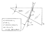
図2を参照して、回転ウェッジシステムを使用する実行を詳細に説明する。センサアレイに対してドキュメントの画像を平行移動する1つの方法は、2つの回転ガラスウェッジを用いて原稿の画像を導くことである。図2はこのスキームを示す。示されているシステムでは、ドキュメント20を照射するフラッシュランプ12a及び12bからの光がレンズ22の1つの焦点面に投射される。それにより、ドキュメント20上のスポットから反射された光がレンズ22によって平行にされる。その後、光は、凸レンズ22と光経路を共有する一連の半透明ウェッジ24及び26により屈折される。
【0020】
示される実施形態では、ウェッジ24及び26は、上部表面が各ウェッジの中心部分に設けられる回転軸に略垂直となるように設置される。これは、共通の光照射路の軸yと一致するのが有利である。
【0021】
図3を参照すると、平行光ビームにおける屈折ウェッジの効果が示される。光ビームの総屈折Δαは、ウェッジ角度β及び屈折率nを有するウェッジ30により生じ、これらは以下の式で示される;
【0022】
小さいαに対しては、Δα=(n−1)β
【0023】
図3で示される特性は、第1ウェッジ24及び第2ウェッジ26の両ウェッジによりもたらされると理解されたい。屈折角Δαはαが小さい場合には入射角αには依存しない。換言すれば、セットアップはウェッジの振動を感知しない。図2に戻ると、凸レンズ32と示される第2レンズは、センサアレイにおいて以下の変位dに画像を平行移動するようにビーム角を変更する。
【0024】
d=FΔα(式中、Fはレンズ32の総焦点距離である)
【0025】
1:1画像倍率の場合、2つのレンズの各々の焦点距離は同一であることが理想である。
【0026】
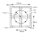
例えば、分解能の2倍(2X)増大の実行に関してシステムを説明する。現在入手可能な200spi センサアレイの場合、センササイズは88μmであり、ピクセルサイズは128μmであるのが典型的である。ピクセルの4分割部分にセンサをステップサイズ64μmでステッピングすることにより、効果的な400spi の分解能で画像を得ることが可能である。4つの対称位置にセンサを移動するためには、単一の回転ウェッジを使用するだけでよい。ドキュメント上のセンサ位置の軌道は図4の円38により示される。焦点距離が30cmである場合、n=1.3として、選択されるウェッジ角βは約1.7分であるべきである。画像走査を完了するためには、軌道が4つの位置40(a)、40(b)、40(c)、及び40(d)に移動された時に、フラッシュランプによる照射が行われるべきである。これらの位置は、図4の円38の円周上に位置されるドット40により示される。照射が行われると、次にこれら4つのフレームが結合されて、有効な400spi 分解能による走査画像が形成される。
【0027】
2Xより大きい分解能増大を達成するために、適切な実施形態は、上で示されたように2つの回転ウェッジを使用する。この実施形態では、ウェッジは異なる速度で回転される。1ピクセル内のセンサの軌道は、各ウェッジにより生じる軌道のベクトル和となる。センサの中心部分がデカルト座標系(xy)の原点となるように選択されると、その軌道を以下のように示し得る。
【0028】
x=A sin(2πf1 t)+B sin(2πf2 +Φ);及び
y=A cos(2πf1 t)+B cos(2πf2 +Φ)
【0029】
これらの式において、A及びBは軌道変位の振幅であり、ウェッジ角に比例する。値f1 及びf2 はそれぞれ、ウェッジ24及びウェッジ26の回転周波数である。式の値Φはウェッジ同士間の位相差であり、tは時間を示す。
【0030】
分解能における3X増大の場合には、以下の条件を適用する。
【0031】
A=B、Φ=0、及びf2 =5f1
【0032】
図5は上記システムの軌道を示す。
【0033】
図6を参照して4X分解能増大の場合の軌道について述べる。このシステムでは、以下の操作条件を適用する。
【0034】
A=B、Φ=0、及びf2 =9f1
【0035】
両ケースにおいて、フラッシュランプ露光のタイミングを正確に制御して、ピクセル内の異なる位置にセンサを位置づけることができる。両ケースにおける軌道は厳密なグリッド上の位置にセンサを置かないが、この特徴はフラッシュランプに対するタイミング信号にランダムなノイズを加えることにより、サンプリング位置をランダム化するように実行されるのが適切である。これはスキャナがハーフトーン画像を画像形成する時のモアレパターンを減少するのに有用である。画像グリッドを正確に構成するために、グリッド上で値を内挿することが有利である。上述のものよりもさらに高い周波数を使用すると共に軌道の対称性を維持することにより、センサの位置を所望のグリッドにかなり近づけることができることが理解される。これは、もたらされる影響が気づかれない程度であるようにセンサ位置をオフセットするように作用する。
【0036】
図7を参照すると、上述の回転ウェッジの代わりに回転ミラーを使用する実施形態が示される。上述のウェッジの基本的な機能がさらに進められるが、それは屈折特性ではなく反射特性により進められる。
【0037】
図7では、図2で示されたものと同じエレメントには同一の参照番号を付与した。基本的な違いは、図2のウェッジ24及び26が図7のミラー50及び52に置き換えられたことである。故に、ミラーが画像をステッピングするように作用する。図2の共通の光アクセスyは、図7の光路y'に類似する。2つのミラーの実施形態における相対的回転周波数は、上述の同じ数学的関係を提供する。
【0038】
以上のことに加えて、円形軌跡でドキュメント又はセンサアレイのいずれかを移動することにより同種の画像形成及び動作が達成され得ることが理解される。回転ウェッジ及びミラーの組み合わせを用いて実行することも適切である。2つの円形動作コンポーネントを正確な周波数にする限りにおいて、同一の効果が達成される。例えば、適切な策として以下のことを含むことができる(しかしこれらに限定されない)。
【0039】
1.ドキュメント及びセンサアレイの両方を移動すること
2.移動するドキュメント及び回転ウェッジ
3.移動するドキュメント及び回転ミラー
4.移動するセンサアレイ及び回転ウェッジ
5.移動するセンサアレイ及び回転ミラー
【0040】
2X増大の場合には、システムにおいて1つの移動部を有するだけでよいことを想起されたい。それは、円状に移動するドキュメント、円状に移動するセンサアレイ、回転ウェッジ、回転ミラー、又は同様物であることが適切である。
【0041】
次に、上述のスーパーピクセル方法を詳細に記載する。スーパーピクセル方法は、1次元的平行移動に必要な動作を単純化する。スーパーピクセル方法は、センサアレイに対してスーパーピクセル設計を提供する。特に図8を参照して、2X分解能増大のスキームを示す。かかるスーパーピクセル構造はブロック60で示される。スーパーピクセルは、従来のピクセルのサイズの2倍のサイズを有するように選択されるのが適切である。スーパーピクセル60の第2ピクセルにおけるセンサ(S2 )は、第1センサ(S1 )に対して1ステップサイズだけ上方にオフセットされる。水平方向に4回ステッピングし、4つの画像フレームを正確な順序でインターリーブすることにより、1つの画像がアレイの空間的分解能の2倍で提供される。この例では、内挿は必要ない。ボックス62内の数は、ステッピングに対する所望のシーケンスを示す。
【0042】
図9は、別のスーパーピクセル構成を示し、この例ではアレイは45°角でステッピングされる。この例でもインターリービングの後で適切な完全な画像が形成され得る。
【0043】
図10は、水平方向ステッピングにより3X分解能増大を達成するようにアレイをステッピングするスキームを示す。部分70は、スーパーピクセルの構造を示す。図10から、上の図9で上述した方法と同様の方法で45°角でもアレイをステッピングできることを理解されたい。
【0044】
ここで述べるスーパーピクセルシステムは、所与のピクセル分解能のアレイを用いてあらゆる複数(N)倍の分解能を達成するように一般化され得る。N倍の分解能増大の場合、適切なことにN個の隣接ピクセルを有するスーパーピクセルを実行することができる(図11参照)。各ピクセルは、エイリアシング防止目的のために1/N2 以上の充填率を有する四角形センサを提供される。中心(複数)は、ピクセルの1つの側に対して、そしてピクセルサイズの1/Nだけ垂直方向に離間されて存在するように複数のピクセル内に配置される。次いでステッピング方向が、ピクセルサイズの1/Nのステップサイズで水平方向に沿って選択される。図11を参照されたい。
【0045】
センサアレイの画質に悪影響を及ぼすことなくピクセルレベルで電子回路を構築するために、センサによりカバーされない空間を使用することも適切であり得る。ピクセルレベルの電子回路は、画像修正、データ処理等に使用できる。残りの領域もまた、接触画像形成において使用されるようなバック照射のために透明にされるのが適切である。
【0046】
本発明の1つの実施形態は、センサアレイに対して画像を線形的に平行移動するために振動ミラーを使用する。図12では、ドキュメント20はフラッシュランプ12(a)及び12(b)からの光で露光される。フラッシュランプ12から放たれた光は、ドキュメント20に伝えられる。そこから反射された光は、光学軸y''に沿って伝わっていく。レンズ22を通る光は、固定ミラー74に導かれ、振動ミラー76に反射される。ミラー76の振動は、ピボット80の回りを回転するミラー76の自由移動端に配置されるプッシャ(pusher)78を用いて行われる。プッシャはピボット80の回りを弧状方向dにミラーをピボットさせる。
【0047】
振動ミラー76から反射された光は、レンズ32に伝わり、それによりセンサアレイ34に焦点合わせされる。振動ミラー76がセンサアレイ34に沿ってレンズ32からの光の焦点fの位置を変化させるように作用することが、この説明から理解される。
【0048】
図13では、別の実施形態を示す。この実施形態では、前と同じく、機能において上述のものと同様のコンポーネントはそのまま同じ番号を付与した。フラッシュランプ12(a)及び12(b)はドキュメント20を照射する。ドキュメント20から反射された光は、光学軸y''' に沿って且つレンズ22を通って投影される。適切な手段(図示せず)を設けて、光学軸y''' に略垂直な方向d'に沿ってレンズ22を横方向に平行移動させる。方向d'に沿うミラー22の往復線形動作は、画像の平行移動を可能にする。
【0049】
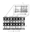
図14は、3X分解能増大の場合のスーパーピクセル設計の一例を示す。他の増大比率のスーパーピクセル設計もまた、図14で示されるものとフォーマットが同じである。スーパーピクセル設計で基本的な考慮すべきことは、製造の設計ルールを満たさなければならないということである。故に、詳細は非常にアプリケーション特定のものであるが、示される例から理解される。
【0050】
図14の示されるスーパーピクセル設計は、他の増大比率に対する基本的なテンプレートを提供する。各特定のスーパーピクセル設計は、アプリケーションに特定のものであり、製造の設計ルールを満たさなければならない。各ピクセルが同じ又は略同じ電気的特性、例えばキャパシタンス、寄生効果等を有することを保証するように、さらなる注意がなされなければならないことも理解される。接触画像形成用に製造されるアレイの場合、スーパーピクセル構造における各センサがそのセンサの隣に同様の透明構造を有すると共に、ドキュメントの均一な露光を保証するために透明領域に対して同一の充填率を有することを確実にするのが有利である。
【0051】
水平方向ステッピングスキームは、対角ステッピングスキーム、及び回転ウェッジ(単数又は複数)及び/又はミラー(単数又は複数)を設けられるものを越える利点を有する。水平方向の平行移動スキームは線形動作を含み、ポストスキャン画像処理も簡単である。
【0052】
水平方向スキームは、センサアレイに対して線形動作を導入することにより実行されるのが適切である。これは、アレイ又はドキュメントを機械的に移動することにより達成され得る。同じ効果は、振動ミラーを用いても適切に達成され得る。この特定の構造は図12を参照して上述した。
【0053】
より高い分解能のためにアレイを線形的にステッピングするためのシステムにおける変形を図15で示す。この図はまた、3X分解能増大を示している。ここでも、基本原理は他の増大比率に対しても同じであることを理解されたい。示されるアレイは、従来の均一なピクセル構造を有する。かかるアレイ内の全画像空間をカバーするために、アレイ又は画像は水平方向から18.43°の角度でステッピングされる。水平方向に沿うステップサイズは、ピクセルサイズの1/3である。この図では、センサは9つのステップ位置のうちの6つに対する高分解能グリッドと一致しない。従って、走査画像(又は露光)に対して高分解能グリッドへの内挿が行われる。これは画像形成装置の速度を減速するが、現在の画像形成装置設計をより高い分解能で使用することを可能にする。
【0054】
一般的なケースでは、従来のピクセル設計及びd/Nのセンササイズ(ここでdはピクセルサイズである)を用いてN倍の分解能増大を達成し得る。
【0055】
アレイは、アークタンジェント(1/N)に等しい角度Θ及び水平方向ステップサイズ(d/N)でドキュメントに対してステッピングされる。
【0056】
本システムはまた、カラー画像走査にも容易に適用される。このシステムは、総画像データを減少して高分解能でドキュメントのカラー画像形成を行う。人の視覚系は、照射システムのものよりも高周波数クロミナンス要素に対してかなり感度が落ちることを理解すべきである。従って、満足のいく品質を有するカラー画像の再生は、画像のクロミナンス要素の低周波数サンプリングにより行われ得る。画質は、最終的な出力フォーマットが達成される手段に依存する。かかる手段は、カラーレーザプリンタ、ビデオモニタ、フォトタイプセッタ等を含む。カラー画像形成は非常に多くのデータを提供するので、処理されるデータを減少すると共に画像形成装置の速度を増すために、三原色のアンダーサンプリングを完了することが、しばしば有利である。
【0057】
2X分解能増大カラー画像形成スキームに対する実行の一例を図16で示す。このシステムでは、ピクセル内ステッピングスキームを用いて上述したパターンでアレイ又は画像をステッピングし、分解能を増大する。このパターンは、画像の三原色を捕捉するために複数回ステッピングされる。より高い分解能増大比率は、上の図6で記載したものと同じステッピングパターンを使用することにより得られる。適切な画像形成システムは、図2及び図7を参照して上述した設計図に見出すことができる。また、カラーフィルタは露光と同期してフラッシュランプの正面でスイッチングされることを理解されたい。
【0058】
人の視覚系は、カラー画像クロミナンスの高周波数要素について感度が高くないので、画像形成装置はまず4つのセンサ位置を通してステッピングされ、(カラーフィルタを用いずに)4つのフレームの白黒画像を捕捉する。アレイのステッピングの第2のパスでは、センサがそれぞれ位置1、位置2、及び位置3にある間に、画像形成装置は赤、青、及び緑の三原色を捕捉する。これら三原色から、Luv系におけるクロミナンス画像u、vが演算される。近似的に、異なるセンサ位置で原色が捕捉され、所与のピクセル分解能での全体的なピクセルの三原色の合理的な表現が得られ得る。故に、高分解能輝度画像は、黒、白、及び2つの低分解能クロミナンス画像の4つのフレームから提供される。次いで、内挿により高分解能グリッドに対して低解像度u、v画像が提供される。故に、12フレームの代わりに7フレームの画像を有するドキュメントの完全なカラー画像形成が提供される。従って速度及びデータ記憶量において比率1.7の向上が得られる。上述の実行を用いて分解能増大の比率をより高くしても速度及び記憶量の向上が増大することを理解されたい。しかしながら、走査画像の画質はそれに伴って低下する。
【0059】
図16の例のカラー画像は、分解能の2X増しを提供された。クロミナンスはより低分解能で捕捉されるが、得られる画質の変化は大抵の場合、カラーレーザ印刷等の多くのアプリケーションでごく僅かである。
【0060】
カラー画像形成はまた、センサアレイに対するドキュメント画像の線形動作ステッピング及び回転フィルタを使用して実行されるのが適切であり、それを以下に詳細に記載する。このような実施形態のように、往復動作の第1のパスで白色光により十分に増大された分解能でドキュメントの黒及び白画像が捕捉される。その後、アレイの相対動作の第2のパスにおいて、ステッピング位置1、2、及び3においてそれぞれ赤、緑、及び青の画像が捕らえられる。(追加の原色セットでも実行され得る。)この点で、ドキュメントのより低い分解能のカラー画像から、より低分解能クロミナンス画像を有する高分解能輝度画像を得ることができる。
【0061】
ドキュメントのカラー露光は、上述のステップ位置1、2、及び3に限定されない。あるアプリケーションは、カラー露光のタイミング、又はカラー露光の数の増大を行って、より良いカラー再現を達成する。このシステムは、上述のようにスーパーピクセル構造にされたアレイだけでなく従来のアレイにも適用され得る。図8、図9、図10、及び図15から明らかなようにカラー露光が発生する時間は重要でない。N、即ち分解能増大ファクタが2より大きい場合には、クロミナンスサンプリングの均一な分布に対してカラー露光の適切なタイミングを選択することができる。
【0062】
以上のシステムから、製造の困難さが根本的な2次元センサアレイのピクセル分解能を制限していることを理解されたい。センサアレイに対してドキュメント画像を移動させながらドキュメントを数回画像形成することにより、かなり高い分解能で画像形成を行うことができる。最終の内挿された画像の分解能は、センササイズに匹敵するように選択されるのが有利なステップサイズにより規定される。画像の移動は、ドキュメントを移動するか、又はアレイを機械的に移動するか、又は回転ウェッジ若しくはミラーを使用するか、のいずれかにより行われることが可能である。小さいセンササイズを有するスーパーピクセル構造は、アレイに対する設計ルールを厳しくすることなく、ピクセル分解能よりかなり高い分解能を達成することが可能である。開示されたシステムは、2次元センサアレイの高速利点を適用して、画像形成システムの分解能を向上する。
【0063】
さらに、人の視覚系ではカラー画像のクロミナンスにおける高周波数要素に対する感度が高くないということを利用して、システムは、画像データを減少された2次元アレイを用いてカラー画像形成の分解能を増大することを可能にする技術を提供する。
【0064】
この提案で述べられた技術の全ては、商業的に入手可能な製品で提供される2次元アモルファスシリコンセンサを用いて実行され得る。
【0065】
好適で変更可能な実施形態を参照して本発明を説明した。本明細書を読み理解するうちに変更及び変形が生じるのは明らかなことである。特許請求の範囲に記載される本発明の趣旨内にある限り、かかる全ての変更及び変形は含まれるものと意図される。
【図面の簡単な説明】
【図1】画像に対してセンサをステッピングすると共に、マルチスキャンを実行することにより達成される実効分解能の3倍増しを示す図である。
【図2】2つの回転ウェッジを有する2次元センサアレイ上でドキュメントの画像をステッピングするためのシステムを示す図である。
【図3】図2の構造において実行される光の屈折を示す図である。
【図4】2倍分解能増大に対するセンサのマッピングを示す図である。
【図5】3倍分解能増大に対するセンサ位置の軌道を示す図である。
【図6】4倍分解能増大に対するセンサ位置の軌道を示す図である。
【図7】回転ミラーを用いて実行される2次元センサアレイと共にドキュメントの画像をステッピングするためのシステムを示す図である。
【図8】アレイが水平方向にステッピングされるスーパーピクセルセンサ構造を用いてマルチスキャンすることによるドキュメントの2倍分解能画像形成を示す概略図である。
【図9】アレイがゲートライン又はデータラインに対して45°角でステッピングされるスーパーピクセルセンサ構造を使用してマルチスキャンすることによるドキュメントの2倍分解能画像形成を示す概略図である。
【図10】アレイが水平方向にステッピングされるスーパーピクセルセンサ構造を使用してマルチスキャンすることによるドキュメントの3倍画像形成を示す図である。
【図11】アレイが水平方向にステッピングされるN倍分解能増大に対するスーパーピクセルセンサ構造を示す概略図である。
【図12】2次元センサアレイ上でドキュメント画像を線形的に平行移動するために振動ミラーを使用するシステムを示す図である。
【図13】投影レンズを横方向に平行移動する2次元センサアレイ上でのドキュメントの画像のステッピングを示す図である。
【図14】3倍分解能能増大アレイに対するスーパーピクセル構造のレイアウトの例を示す図である。
【図15】従来のピクセル設計を用いる3倍分解能増大に対するアレイの線形的ステッピングを示す図である。
【図16】データ率を減少しての高分解能カラー画像形成を示す図である。
【符号の説明】
20 ドキュメント
12a、12b フラッシュランプ
24、26 ウェッジ
22、32 レンズ
34 センサアレイ[0001]
BACKGROUND OF THE INVENTION
The present invention relates to electronic imaging techniques, and more particularly to obtaining high resolution images using a relatively low resolution image sensor array.
[0002]
The invention is particularly applicable to digital image capture arrays having a relatively small area from which information is extracted, which relates to the overall pixel area defined on the specimen.
[0003]
The invention will be described with particular reference to obtaining such resolution conversion. However, the present invention acquires additional or redundant information during the scanning process, allowing higher resolution or completeness image capture.
[0004]
[Prior art]
Many of today's image capture, manipulation, and printing tasks are performed through digital processing. However, hard copy or print copy is still a major step in most applications.
[0005]
Conversion between the hard copy image and its digital representation is performed by a scanner. Such scanners typically include a sensor array such as a charge coupled device (CCD). In such a CCD array, the actual image of the specimen is focused on the planar shaped array. Each CCD element in the array provides a digital signal representing the light exposed to it. The unique manufacturing technique in the CCD structure provides a finite distance between each element of the array. Each array element thus provides a digital signal representative of a small portion of the corresponding image obtained from the associated specimen. Therefore, information in the image cracks is lost. This results in a degradation or reduction in image integrity due to the visual loss of data associated with this.
[0006]
[Problems to be solved by the invention]
The present invention provides a new and improved system that overcomes the above and other problems, as well as the acquisition of high resolution images by using multiple scans from the sensors of the individual sensor elements of the sensor array. A digital image capture system is provided.
[0007]
[Means for Solving the Problems]
In accordance with the present invention, the increased resolution image scanner includes a sensor array. Each sensor in the array produces a signal that indicates the light energy focused on it. Light reflected from the associated specimen is transmitted to the array of sensor elements. Each sensor element then generates a signal indicative of the corresponding picture element (“pixel”) of the associated image. This associated specimen is then newly oriented relative to the sensor array. With this new orientation, each sensor element of the array obtains another signal indicative of a second portion of the same specimen. The combination of both data sets then provides a high resolution digitized image of the relevant sample.
[0008]
In accordance with a more limited aspect of the present invention, the acquisition of the second signal by reorienting the sensor array relative to the specimen may be performed from a different portion of the same pixel from which the sensor has acquired the first reading. To obtain a second reading. This is suitably performed by placing either a rotating mirror or a rotating lens between the sensor array and the associated specimen.
[0009]
According to another aspect of the invention, the second signal from each of the sensors is obtained from another pixel, i.e., a pixel that is different from the pixel from which that particular sensor element obtained its first reading. This is suitably done by a mirror placed between the sensor array and the associated specimen. Necessary displacement is performed by the movement of the mirror.
[0010]
In accordance with the first aspect of the present invention, the increased resolution image scanner includes an array of sensors, each sensor of the array generating a signal representative of a first small portion of a selected pixel of the associated sample. Used for. The increased resolution image scanner includes orientation means for directing each of the sensors relative to an associated sample to generate a signal representative of at least a second small portion of each selected pixel.
[0011]
An advantage of the present invention is that it provides a system where acquisition of images with higher resolution can be achieved with a relatively coarse array of sensor elements.
[0012]
Another advantage of the present invention is to provide a system that matches the actual captured image data with the desired resolution of the associated acquired image.
[0013]
Yet another advantage of the present invention is to provide an image capture system that provides additional or redundant information provided in combination in the resulting acquired image.
[0014]
Further advantages of the present invention will become apparent to those skilled in the art upon reading and understanding this specification.
[0015]
DETAILED DESCRIPTION OF THE INVENTION
Reference is now made to the drawings, which are intended to illustrate preferred embodiments of the invention and are not intended to limit the invention. FIG. 1 shows the basic method by which the effective resolution is increased by a factor of 3 (3X) by stepping the sensor over the image and performing a multi-scan. If the sensor size is smaller than the pixel size in the array, the resolution of the sensor array is defined by the pixel size. The system corrects this. By stepping the sensor so that the image is created by multi-scan, the resolution depends on the size of the sensor, not the pixel size.
[0016]
As can be seen from FIG. 1, the pixel boundary for
[0017]
The present invention teaches several methods for translating an image relative to a sensor array. For example, the sensor stepping for various locations 1-9 within the
[0018]
The intra-pixel step method operates to position the array relative to the image such that the sensor area covers the complete area of one array pixel, as is apparent in FIG. This is suitably done using a rotating glass wedge or rotating mirror, both of which are described below. Any suitable optical manipulation can act to achieve the same result, for example, by rotating the document and / or sensor array in combination with a rotating wedge or rotating mirror.
[0019]
With reference to FIG. 2, the implementation using the rotating wedge system will be described in detail. One way to translate the document image relative to the sensor array is to use two rotating glass wedges to guide the document image. FIG. 2 illustrates this scheme. In the system shown, light from flash lamps 12 a and 12 b illuminating
[0020]
In the embodiment shown, the
[0021]
Referring to FIG. 3, the effect of a refractive wedge on a collimated light beam is shown. The total refraction Δα of the light beam is caused by a
[0022]
For small α, Δα = (n−1) β
[0023]
It should be understood that the characteristics shown in FIG. 3 are provided by both the
[0024]
d = FΔα (where F is the total focal length of the lens 32)
[0025]
In the case of 1: 1 image magnification, the focal length of each of the two lenses is ideally the same.
[0026]
For example, the system will be described with respect to performing a double (2X) increase in resolution. For currently available 200 spi sensor arrays, the sensor size is typically 88 μm and the pixel size is typically 128 μm. By stepping the sensor on a quadrant of pixels with a step size of 64 μm, it is possible to obtain an image with an effective 400 spi resolution. To move the sensor to four symmetrical positions, only a single rotating wedge need be used. The trajectory of the sensor position on the document is indicated by
[0027]
In order to achieve a resolution increase greater than 2X, a suitable embodiment uses two rotating wedges as indicated above. In this embodiment, the wedge is rotated at different speeds. The trajectory of the sensor within one pixel is the vector sum of the trajectories produced by each wedge. If the center of the sensor is selected to be the origin of the Cartesian coordinate system (xy), its trajectory can be shown as follows:
[0028]
x = A sin (2πf1t) + B sin (2πf2+ Φ); and
y = A cos (2πf1t) + B cos (2πf2+ Φ)
[0029]
In these equations, A and B are orbital displacement amplitudes, which are proportional to the wedge angle. Value f1And f2Are the rotational frequencies of the
[0030]
For a 3X increase in resolution, the following conditions apply:
[0031]
A = B, Φ = 0, and f2= 5f1
[0032]
FIG. 5 shows the trajectory of the system.
[0033]
The trajectory in the case of 4X resolution increase will be described with reference to FIG. In this system, the following operating conditions are applied.
[0034]
A = B, Φ = 0, and f2= 9f1
[0035]
In both cases, the timing of the flash lamp exposure can be precisely controlled to position the sensor at different locations within the pixel. The trajectory in both cases does not place the sensor at a precise grid location, but this feature is appropriate to be implemented to randomize the sampling location by adding random noise to the timing signal for the flashlamp. is there. This is useful for reducing the moire pattern when the scanner forms a halftone image. In order to accurately construct the image grid, it is advantageous to interpolate values on the grid. It will be appreciated that by using higher frequencies than those described above and maintaining orbital symmetry, the position of the sensor can be made much closer to the desired grid. This acts to offset the sensor position so that the resulting effect is not noticeable.
[0036]
Referring to FIG. 7, an embodiment is shown that uses a rotating mirror instead of the rotating wedge described above. The basic function of the wedge described above is further advanced, but it is advanced not by refractive properties but by reflective properties.
[0037]
In FIG. 7, the same elements as those shown in FIG. 2 are given the same reference numerals. The basic difference is that the
[0038]
In addition to the foregoing, it will be appreciated that similar imaging and operation can be achieved by moving either the document or the sensor array in a circular trajectory. It is also appropriate to perform with a combination of rotating wedges and mirrors. As long as the two circular motion components are at the correct frequency, the same effect is achieved. For example, suitable measures can include (but are not limited to) the following:
[0039]
1. Moving both documents and sensor arrays
2. Moving document and rotating wedge
3. Moving document and rotating mirror
4). Moving sensor array and rotating wedge
5. Moving sensor array and rotating mirror
[0040]
Recall that in the case of 2X augmentation, it is only necessary to have one moving part in the system. Suitably it is a circularly moving document, a circularly moving sensor array, a rotating wedge, a rotating mirror, or the like.
[0041]
The above superpixel method will now be described in detail. The superpixel method simplifies the operations required for one-dimensional translation. The superpixel method provides a superpixel design for the sensor array. With particular reference to FIG. 8, a scheme for 2X resolution enhancement is shown. Such a superpixel structure is indicated by block 60. The superpixel is suitably selected to have a size that is twice the size of a conventional pixel. Sensor (S) in the second pixel of the superpixel 602) Is the first sensor (S1) Is offset upward by one step size. By stepping four times horizontally and interleaving the four image frames in the correct order, one image is provided at twice the spatial resolution of the array. In this example, no interpolation is necessary. The number in
[0042]
FIG. 9 shows another superpixel configuration, in this example the array is stepped at a 45 ° angle. In this example as well, a suitable complete image can be formed after interleaving.
[0043]
FIG. 10 shows a scheme for stepping an array to achieve a 3X resolution increase by horizontal stepping.
[0044]
The superpixel system described herein can be generalized to achieve any multiple (N) times resolution using an array of a given pixel resolution. For a resolution increase of N times, it is possible to implement a superpixel with N neighboring pixels as appropriate (see FIG. 11). Each pixel is 1 / N for anti-aliasing purposes2A rectangular sensor having the above filling rate is provided. The center (s) are located within the pixels such that they lie on one side of the pixel and are vertically spaced by 1 / N of the pixel size. The stepping direction is then selected along the horizontal direction with a step size of 1 / N of the pixel size. Please refer to FIG.
[0045]
It may also be appropriate to use the space not covered by the sensor to build the electronic circuit at the pixel level without adversely affecting the image quality of the sensor array. Pixel level electronics can be used for image correction, data processing, and the like. The remaining areas are also suitably made transparent for back illumination as used in contact imaging.
[0046]
One embodiment of the present invention uses a vibrating mirror to translate the image linearly relative to the sensor array. In FIG. 12, the
[0047]
The light reflected from the vibrating
[0048]
FIG. 13 shows another embodiment. In this embodiment, as before, components similar to those described above in function are assigned the same numbers. Flash lamps 12 (a) and 12 (b) illuminate the
[0049]
FIG. 14 shows an example of a superpixel design for 3X resolution increase. Other augmented ratio superpixel designs are also in the same format as shown in FIG. A basic consideration in superpixel design is that manufacturing design rules must be met. Thus, the details are very application specific but will be understood from the examples shown.
[0050]
The superpixel design shown in FIG. 14 provides a basic template for other growth rates. Each specific superpixel design is application specific and must meet manufacturing design rules. It is also understood that additional care must be taken to ensure that each pixel has the same or substantially the same electrical characteristics, such as capacitance, parasitic effects, and the like. In the case of an array manufactured for contact imaging, each sensor in the superpixel structure has a similar transparent structure next to that sensor and the same filling for the transparent area to ensure uniform exposure of the document It is advantageous to ensure that it has a rate.
[0051]
Horizontal stepping schemes have advantages over diagonal stepping schemes and those provided with rotating wedge (s) and / or mirror (s). The horizontal translation scheme includes linear motion and post-scan image processing is simple.
[0052]
The horizontal scheme is suitably implemented by introducing linear motion to the sensor array. This can be accomplished by mechanically moving the array or document. The same effect can be appropriately achieved using a vibrating mirror. This particular structure was described above with reference to FIG.
[0053]
A variation in the system for linearly stepping the array for higher resolution is shown in FIG. This figure also shows a 3X resolution increase. Again, it should be understood that the basic principle is the same for other growth rates. The array shown has a conventional uniform pixel structure. To cover the entire image space in such an array, the array or image is stepped at an angle of 18.43 ° from the horizontal. The step size along the horizontal direction is 1/3 of the pixel size. In this figure, the sensors do not coincide with the high resolution grid for 6 of the 9 step positions. Therefore, the scanned image (or exposure) is interpolated into a high resolution grid. This reduces the speed of the image forming apparatus, but allows the current image forming apparatus design to be used with higher resolution.
[0054]
In the general case, a conventional pixel design and d / N sensor size (where d is the pixel size) can be used to achieve N times the resolution increase.
[0055]
The array is stepped on the document with an angle Θ equal to the arctangent (1 / N) and a horizontal step size (d / N).
[0056]
The system is also easily applied to color image scanning. This system reduces the total image data and forms a color image of the document with high resolution. The human visual system has a higher frequency than that of the illumination systemChrominanceIt should be understood that the sensitivity to elements is considerably reduced. Therefore, reproduction of color images with satisfactory qualityChrominanceThis can be done by low frequency sampling of the elements. The image quality depends on the means by which the final output format is achieved. Such means include color laser printers, video monitors, phototype setters and the like. Since color imaging provides a great deal of data, it is often advantageous to complete the undersampling of the three primary colors in order to reduce the data processed and increase the speed of the imaging device.
[0057]
An example of an implementation for a 2X resolution enhanced color imaging scheme is shown in FIG. In this system, an intra-pixel stepping scheme is used to step the array or image with the pattern described above to increase resolution. This pattern is stepped multiple times to capture the three primary colors of the image. A higher resolution increase ratio can be obtained by using the same stepping pattern as described in FIG. 6 above. A suitable imaging system can be found in the blueprints described above with reference to FIGS. It should also be understood that the color filter is switched in front of the flash lamp synchronously with the exposure.
[0058]
The human visual system is a color imageChrominanceThe image forming device is first stepped through the four sensor positions to capture four frames of black and white image (without using a color filter). In the second pass of the array stepping, the imaging device captures the three primary colors red, blue, and green while the sensors are at
[0059]
The color image in the example of FIG. 16 was provided with a 2X increase in resolution.ChrominanceAre captured at a lower resolution, but the resulting change in image quality is often negligible in many applications such as color laser printing.
[0060]
Color imaging is also suitably performed using a linear motion stepping and rotation filter of the document image relative to the sensor array, which is described in detail below. As in such an embodiment, a black and white image of the document is captured with a sufficiently increased resolution by white light in the first pass of the reciprocating motion. Thereafter, in the second pass of the relative movement of the array, red, green and blue images are captured at stepping
[0061]
The color exposure of the document is not limited to the above-described
[0062]
From the above system, it should be understood that manufacturing difficulties limit the pixel resolution of the underlying two-dimensional sensor array. By forming the document several times while moving the document image with respect to the sensor array, it is possible to form an image with a considerably high resolution. The resolution of the final interpolated image is defined by a step size that is advantageously chosen to be comparable to the sensor size. The movement of the image can be done either by moving the document, moving the array mechanically, or using a rotating wedge or mirror. A superpixel structure with a small sensor size can achieve a resolution much higher than the pixel resolution without strict design rules for the array. The disclosed system applies the high speed advantages of a two-dimensional sensor array to improve the resolution of the imaging system.
[0063]
Furthermore, in the human visual system, color imagesChrominanceTaking advantage of the lack of sensitivity to high frequency elements in the system, the system provides a technique that allows the resolution of color imaging to be increased using a reduced two-dimensional array of image data.
[0064]
All of the techniques described in this proposal can be implemented using a two-dimensional amorphous silicon sensor provided in a commercially available product.
[0065]
The invention has been described with reference to the preferred and changeable embodiments. Obviously, changes and modifications will occur while reading and understanding this specification. All such changes and modifications are intended to be included within the scope of the present invention as set forth in the appended claims.
[Brief description of the drawings]
FIG. 1 illustrates a threefold increase in effective resolution achieved by stepping a sensor over an image and performing a multi-scan.
FIG. 2 illustrates a system for stepping an image of a document on a two-dimensional sensor array having two rotating wedges.
FIG. 3 is a diagram showing light refraction performed in the structure of FIG. 2;
FIG. 4 shows sensor mapping for a double resolution increase.
FIG. 5 is a diagram illustrating a trajectory of a sensor position with respect to an increase in resolution of 3 times.
FIG. 6 is a diagram illustrating a trajectory of a sensor position with respect to a 4-fold resolution increase.
FIG. 7 illustrates a system for stepping an image of a document with a two-dimensional sensor array performed using a rotating mirror.
FIG. 8 is a schematic diagram illustrating double resolution imaging of a document by multi-scanning using a superpixel sensor structure in which the array is stepped horizontally.
FIG. 9 is a schematic diagram illustrating double-resolution imaging of a document by multi-scanning using a superpixel sensor structure in which the array is stepped at 45 ° angles to gate lines or data lines.
FIG. 10 illustrates triple image formation of a document by multi-scanning using a superpixel sensor structure where the array is stepped horizontally.
FIG. 11 is a schematic diagram illustrating a superpixel sensor structure for an N-fold resolution increase in which the array is stepped horizontally.
FIG. 12 illustrates a system that uses a vibrating mirror to linearly translate a document image on a two-dimensional sensor array.
FIG. 13 is a diagram illustrating stepping of an image of a document on a two-dimensional sensor array in which a projection lens is translated in the horizontal direction.
FIG. 14 is a diagram showing an example of a layout of a superpixel structure for a triple resolution enhancement array.
FIG. 15 shows linear stepping of an array for a 3 × resolution increase using a conventional pixel design.
FIG. 16 is a diagram showing high-resolution color image formation with a reduced data rate.
[Explanation of symbols]
20 documents
12a, 12b Flash lamp
24, 26 wedge
22, 32 lenses
34 Sensor array
Claims (4)
複数のセンサのアレイを含み、当該複数のセンサは、第 1 のスキャンの間は標本の選択されたピクセルの第1の小部分を表す信号を生成するように距離を置いて配置され、前記選択されたピクセルが第 1 の小部分より大きな領域を有し、
非分割信号として前記データ信号を変位させるための第2のスキャンの間、前記標本の前記データ信号について相対的に前記センサのそれぞれを改めて方向づけし、前記センサ間の前記距離のために前記スキャナのアレイが読み取れなかった前記標本の一つの範囲をなす各選択されたピクセルの少なくとも第2の小部分を表す第2の信号を以下の式に従って生成する、前記標本と前記アレイとの間に配置された方向づけ手段を含み、上記式が
x=A sin (2πf 1 t)+B sin (2πf 2 +Φ)及び
y=A cos (2πf 1 t)+B cos (2πf 2 +Φ)
であって、これらの式は前記センサの中心部分の軌道を示し、xとyとは前記センサの中心部分であり、変数A及びBは軌道変位の振幅であり、変数f 1 及びf 2 は回転周波数であり、変数Φは前記方向づけ手段の要素間の位相差であり、変数tは時間を示し、前記中心部分の軌道が、増大された解像度を持つ一つのピクセルグリッドに重なるように前記変数が選択されることを特徴とする、
分解能増大画像スキャナ。 An increased resolution image scanner for generating a data signal representative of the image of the specimen from which the image is formed , wherein the data signal has a resolution greater than the resolution of the sensor array of the scanner;
Includes a plurality of arrays of sensors, the plurality of sensors during the first scan is arranged at a distance to generate a signal representative of a first small portion of the selected pixels of the sample, the selection The resulting pixel has a larger area than the first sub-portion ,
During a second scan for displacing the data signal as an undivided signal, each of the sensors is reoriented relative to the data signal of the sample, and because of the distance between the sensors, Arranged between the sample and the array , generating a second signal representing at least a second sub-portion of each selected pixel that forms a range of the sample from which the array could not be read according to the following equation: Orientation means, and the above formula
x = A sin (2πf 1 t) + B sin (2πf 2 + Φ) and
y = A cos (2πf 1 t) + B cos (2πf 2 + Φ)
Where these equations represent the trajectory of the central part of the sensor, x and y are the central part of the sensor, the variables A and B are the amplitudes of the trajectory displacement, and the variables f 1 and f 2 are The rotation frequency, the variable Φ is the phase difference between the elements of the directing means, the variable t indicates time, and the trajectory of the central part overlaps one pixel grid with increased resolution. Is selected ,
Increased resolution image scanner.
前記第1及び前記第2の回転透明ウェッジと前記関連標本との間に配置された前記光軸を共有する第1レンズと、
前記第1及び前記第2の回転透明ウェッジと前記センサのアレイとの間に配置された前記光軸を共有する第2レンズと、
をさらに備える、請求項2に記載の分解能増大画像スキャナ。The directing means includes a first rotating transparent wedge and a second rotating transparent wedge, and the first rotating transparent wedge and the second rotating transparent wedge have a common optical axis, and the optical axis is Disposed between the associated specimen and the array of sensors;
A first lens sharing the optical axis disposed between the first and second rotating transparent wedges and the associated specimen;
A second lens sharing the optical axis disposed between the first and second rotating transparent wedges and the array of sensors;
The increased resolution image scanner of claim 2, further comprising:
Applications Claiming Priority (2)
| Application Number | Priority Date | Filing Date | Title |
|---|---|---|---|
| US08/485,847 US6005682A (en) | 1995-06-07 | 1995-06-07 | Resolution enhancement by multiple scanning with a low-resolution, two-dimensional sensor array |
| US485847 | 1995-06-07 |
Publications (2)
| Publication Number | Publication Date |
|---|---|
| JPH099005A JPH099005A (en) | 1997-01-10 |
| JP3874841B2 true JP3874841B2 (en) | 2007-01-31 |
Family
ID=23929657
Family Applications (1)
| Application Number | Title | Priority Date | Filing Date |
|---|---|---|---|
| JP15887096A Expired - Lifetime JP3874841B2 (en) | 1995-06-07 | 1996-05-30 | Increased resolution image scanner |
Country Status (3)
| Country | Link |
|---|---|
| US (1) | US6005682A (en) |
| EP (1) | EP0748108A3 (en) |
| JP (1) | JP3874841B2 (en) |
Families Citing this family (26)
| Publication number | Priority date | Publication date | Assignee | Title |
|---|---|---|---|---|
| EP0977068A3 (en) * | 1998-07-31 | 2000-04-19 | Loyal Port Company Limited | Image inverting device |
| US6194718B1 (en) * | 1998-09-23 | 2001-02-27 | Applied Materials, Inc. | Method for reducing aliasing effects in scanning beam microscopy |
| TW404114B (en) * | 1999-01-29 | 2000-09-01 | Microtek Int Inc | Image scanner with image correction function |
| US6512539B1 (en) * | 1999-09-29 | 2003-01-28 | Xerox Corporation | Document periscope |
| US7123292B1 (en) | 1999-09-29 | 2006-10-17 | Xerox Corporation | Mosaicing images with an offset lens |
| JP4182638B2 (en) * | 2000-11-07 | 2008-11-19 | コニカミノルタホールディングス株式会社 | Imaging apparatus, method for synthesizing captured image, computer-readable recording medium recording image processing program, and imaging system |
| EP1436981A1 (en) | 2001-09-11 | 2004-07-14 | Deltapix APS | A method and apparatus for producing a high resolution image |
| EP1301027A1 (en) * | 2001-10-05 | 2003-04-09 | Abscondenda AB | Method and device for improved image resolution or image comparison using high speed parallel processing |
| US6906305B2 (en) * | 2002-01-08 | 2005-06-14 | Brion Technologies, Inc. | System and method for aerial image sensing |
| US6828542B2 (en) * | 2002-06-07 | 2004-12-07 | Brion Technologies, Inc. | System and method for lithography process monitoring and control |
| US6642497B1 (en) * | 2002-06-14 | 2003-11-04 | Hewlett-Packard Development Company, Lp. | System for improving image resolution via sensor rotation |
| US6807503B2 (en) | 2002-11-04 | 2004-10-19 | Brion Technologies, Inc. | Method and apparatus for monitoring integrated circuit fabrication |
| DE10259667B4 (en) * | 2002-12-18 | 2004-09-16 | Lfk-Lenkflugkörpersysteme Gmbh | Process for enlarging the field of view of a focal plane array camera |
| US20040120017A1 (en) * | 2002-12-20 | 2004-06-24 | Miller Mindy Lee | Method and apparatus for compensating for assembly and alignment errors in sensor assemblies |
| US6759297B1 (en) | 2003-02-28 | 2004-07-06 | Union Semiconductor Technology Corporatin | Low temperature deposition of dielectric materials in magnetoresistive random access memory devices |
| US7053355B2 (en) | 2003-03-18 | 2006-05-30 | Brion Technologies, Inc. | System and method for lithography process monitoring and control |
| EP1594321A3 (en) * | 2004-05-07 | 2006-01-25 | Dialog Semiconductor GmbH | Extended dynamic range in color imagers |
| US7129460B1 (en) * | 2005-09-02 | 2006-10-31 | Olson Gaylord G | Electronic imaging apparatus with high resolution and wide field of view and method |
| US8072502B2 (en) | 2005-12-12 | 2011-12-06 | Sony Ericsson Mobile Communications Ab | Multi-mega pixel resolution with small sensor |
| NO332432B1 (en) * | 2008-08-12 | 2012-09-17 | Kongsberg Seatex As | System for detection and imaging of objects in the trajectory of marine vessels |
| US8547426B2 (en) * | 2009-06-15 | 2013-10-01 | Identix Incorporated | Low settle time micro-scanning system |
| US7990528B2 (en) * | 2009-09-29 | 2011-08-02 | Xerox Corporation | High resolution linear image sensing using multi-row low resolution image sensor |
| IL219773A (en) | 2012-05-13 | 2015-09-24 | Elbit Sys Electro Optics Elop | Apparatus and method for increasing the resolution of a cryogenically cooled and vacuum-sealed infrared imaging detector |
| DE102016113978B4 (en) * | 2016-07-28 | 2021-09-02 | Lilas Gmbh | Device for deflecting laser radiation or for deflecting light |
| US10642049B2 (en) * | 2018-04-25 | 2020-05-05 | Apple Inc. | Head-mounted device with active optical foveation |
| IL274418B (en) | 2020-05-03 | 2021-12-01 | Elbit Systems Electro Optics Elop Ltd | Systems and methjods for enhanced motion detection, object tracking, situational awareness and super-resolution video using microscanned images |
Family Cites Families (12)
| Publication number | Priority date | Publication date | Assignee | Title |
|---|---|---|---|---|
| US4168126A (en) * | 1977-07-05 | 1979-09-18 | Altman Associates, Inc. | Electro-optical measuring system using precision light translator |
| DE3630739C1 (en) * | 1986-09-10 | 1988-04-07 | Zeiss Carl Fa | Method for data pick-up by means of detector arrays and devices for carrying out the methods |
| US4755876A (en) * | 1987-07-27 | 1988-07-05 | Eastman Kodak Company | Image scanner |
| US4923263A (en) * | 1988-09-22 | 1990-05-08 | The United States Of America As Represented By The Secretary Of The Army | Rotating mirror optical scanning device |
| US4972270A (en) * | 1989-04-17 | 1990-11-20 | Stephen Kurtin | Facsimile recorder with acutely mounted staggered array ink jet printhead |
| JP2753541B2 (en) * | 1990-02-19 | 1998-05-20 | 株式会社ニコン | Still image pickup device |
| GB2250884B (en) * | 1990-12-07 | 1995-05-10 | Philips Electronic Associated | Optical image sensing systems |
| US5267056A (en) * | 1991-01-03 | 1993-11-30 | Xerox Corporation | Right reading image for read/write components co-mounted on a single X-Y carriage |
| GB9103262D0 (en) * | 1991-02-15 | 1991-08-21 | Marconi Gec Ltd | Optical systems |
| WO1993014594A1 (en) * | 1992-01-14 | 1993-07-22 | Michael Sussman | Image input device having optical deflection elements for capturing multiple sub-images |
| JP3380913B2 (en) * | 1992-06-11 | 2003-02-24 | ソニー株式会社 | Solid-state imaging device |
| US5301042A (en) * | 1993-01-04 | 1994-04-05 | Eastman Kodak Company | Imaging platform support to permit dithering motion |
-
1995
- 1995-06-07 US US08/485,847 patent/US6005682A/en not_active Expired - Lifetime
-
1996
- 1996-05-30 JP JP15887096A patent/JP3874841B2/en not_active Expired - Lifetime
- 1996-06-05 EP EP96304093A patent/EP0748108A3/en not_active Withdrawn
Also Published As
| Publication number | Publication date |
|---|---|
| US6005682A (en) | 1999-12-21 |
| JPH099005A (en) | 1997-01-10 |
| EP0748108A2 (en) | 1996-12-11 |
| EP0748108A3 (en) | 1999-05-06 |
Similar Documents
| Publication | Publication Date | Title |
|---|---|---|
| JP3874841B2 (en) | Increased resolution image scanner | |
| US6414760B1 (en) | Image scanner with optical waveguide and enhanced optical sampling rate | |
| US4626901A (en) | Image processing apparatus using multiple dither matrices | |
| JPH0813088B2 (en) | Image reader | |
| JPH08274956A (en) | Image scanner | |
| JPH06115175A (en) | Device of scanning recording medium by light beam | |
| EP0213188A1 (en) | Apparatus for scanning and sampling real images | |
| JP2001197255A (en) | Image reader and image reading method using the device | |
| JP3625384B2 (en) | Image reading device | |
| JPH0443766A (en) | Original reader | |
| US5327251A (en) | Image scanning apparatus | |
| JPH11234482A (en) | Image reader | |
| JPH0514465B2 (en) | ||
| JP2892593B2 (en) | Image input device | |
| JP2001144899A (en) | Picture reader adjusting method | |
| JPS59104619A (en) | Optical scanner | |
| JP2000214404A (en) | Method and device for correcting coma in high-resolution scanner | |
| JPH06197250A (en) | Video camera | |
| JPH01278182A (en) | Image sensor camera | |
| JPH04133570A (en) | Image recorder | |
| JPH0376463A (en) | Facsimile equipment | |
| JPS6318863A (en) | Image reader | |
| JPS60218618A (en) | Original reading method | |
| JPH08220459A (en) | Rotary polygon mirror used in optical device | |
| JPH01265663A (en) | Picture input device |
Legal Events
| Date | Code | Title | Description |
|---|---|---|---|
| A977 | Report on retrieval |
Free format text: JAPANESE INTERMEDIATE CODE: A971007 Effective date: 20050715 |
|
| A131 | Notification of reasons for refusal |
Free format text: JAPANESE INTERMEDIATE CODE: A131 Effective date: 20050726 |
|
| A521 | Request for written amendment filed |
Free format text: JAPANESE INTERMEDIATE CODE: A523 Effective date: 20051026 |
|
| TRDD | Decision of grant or rejection written | ||
| A01 | Written decision to grant a patent or to grant a registration (utility model) |
Free format text: JAPANESE INTERMEDIATE CODE: A01 Effective date: 20060926 |
|
| A61 | First payment of annual fees (during grant procedure) |
Free format text: JAPANESE INTERMEDIATE CODE: A61 Effective date: 20061025 |
|
| R150 | Certificate of patent or registration of utility model |
Free format text: JAPANESE INTERMEDIATE CODE: R150 |
|
| FPAY | Renewal fee payment (event date is renewal date of database) |
Free format text: PAYMENT UNTIL: 20091102 Year of fee payment: 3 |
|
| FPAY | Renewal fee payment (event date is renewal date of database) |
Free format text: PAYMENT UNTIL: 20101102 Year of fee payment: 4 |
|
| FPAY | Renewal fee payment (event date is renewal date of database) |
Free format text: PAYMENT UNTIL: 20111102 Year of fee payment: 5 |
|
| FPAY | Renewal fee payment (event date is renewal date of database) |
Free format text: PAYMENT UNTIL: 20121102 Year of fee payment: 6 |
|
| FPAY | Renewal fee payment (event date is renewal date of database) |
Free format text: PAYMENT UNTIL: 20121102 Year of fee payment: 6 |
|
| FPAY | Renewal fee payment (event date is renewal date of database) |
Free format text: PAYMENT UNTIL: 20131102 Year of fee payment: 7 |
|
| R250 | Receipt of annual fees |
Free format text: JAPANESE INTERMEDIATE CODE: R250 |
|
| R250 | Receipt of annual fees |
Free format text: JAPANESE INTERMEDIATE CODE: R250 |
|
| EXPY | Cancellation because of completion of term |