JP3718577B2 - Radio receiver and radio reception method - Google Patents
Radio receiver and radio reception method Download PDFInfo
- Publication number
- JP3718577B2 JP3718577B2 JP07805697A JP7805697A JP3718577B2 JP 3718577 B2 JP3718577 B2 JP 3718577B2 JP 07805697 A JP07805697 A JP 07805697A JP 7805697 A JP7805697 A JP 7805697A JP 3718577 B2 JP3718577 B2 JP 3718577B2
- Authority
- JP
- Japan
- Prior art keywords
- signal
- detected
- correlation value
- reference signal
- reception method
- Prior art date
- Legal status (The legal status is an assumption and is not a legal conclusion. Google has not performed a legal analysis and makes no representation as to the accuracy of the status listed.)
- Expired - Fee Related
Links
Images


Landscapes
- Digital Transmission Methods That Use Modulated Carrier Waves (AREA)
- Synchronisation In Digital Transmission Systems (AREA)
Description
【0001】
【発明の属する技術分野】
本発明は、無線受信機及び無線受信方法に関し、例えば音声信号を符号化して送受信するデジタル移動電話装置等に用いて好適なものである。
【0002】
【従来の技術および発明が解決しようとする課題】
従来からデジタル移動電話装置を持つデジタルセルラシステムでは、符号化された音声信号を使用した時分割多重方式の使用により、1つのチャンネルを複数の端末機器が同時に使用してきた。
更に具体的に言えば、端末は、電波が到達すると、例えば124チャンネル全てを順番に走査して、最も強い電界強度のチャンネルを選択する。
【0003】
そして、端末は各地域に割当てられた制御チャンネルを検出してそれを受信する。このシステムでは、1つのセル当たり利用可能なチャンネル数は124である。制御チャンネルの位置は、124チャンネルのうちの特定チャンネルに固定してはいない。従って、このシステムの装置は全ての124チャンネルを順次走査して、電界強度の順に並び換えを行って、並び換えられたリストの中から周波数制御チャンネル(FCCH)を探索する。こうして探索された制御チャンネルは、タイムスロットの形成や各種情報の送信の為に使用され、このデジタルセルラシステムでは各端末から基地局への情報の送信・隣接基地局間の情報伝送・基地局からの端末機の呼出しに使用される。
【0004】
端末はこの制御チャンネルに周期的に挿入された信号を検出する。そして、この信号に基づいて動作タイミングを調整すると同時に、必要な情報の存在するタイム・スロットの概略の位置を検出する。
【0005】
周波数制御チャンネルの信号は、それがデジタル移動電話端末で復号された際に“0”の値が所定ビット数だけ連続するようなビットパターンで同期されており、このデータは差動符号化されたあとGMSK(ガウシャン・フィルタード・ミニマム・シフト・キーイング)変調されて送信される。図1に示すように、周波数制御チャンネルの信号は位相差が90°の正弦波に情報を変調したI信号及びQ信号の複合として表される。この信号は、搬送波周波数から+67.7kHzだけオフセットしている。
【0006】
デジタル移動電話装置は、周波数制御チャンネルの信号成分を受信信号からバンドパス・フィルタで抜き出してそのタイミングを検出し、検出されたタイミングに基づいて全体の動作を同期させる。このようにバンドパス・フィルタで周波数制御チャンネルの信号成分を抜き出す場合、バンドパス・フィルタの帯域幅が狭いほど検出精度は高くなる。しかし、帯域幅を狭くすれば応答特性は悪くなる。
【0007】
GSM方式のデジタルセルラ・システムの周波数制御チャンネルの信号の持続期間は550μsと短いため、バンドパス・フィルタの応答特性が悪くなると周波数制御チャンネルを検出するのは困難となる。
【0008】
更にデジタル移動電話装置では、ドップラー偏移によって周波数がずれたり、周波数制御チャンネルの信号以外のデータが周波数制御チャンネルの信号と同じ周波数であることがある。従ってバンドパス・フィルタを使うと、周波数制御チャンネルの信号のタイミングを誤って検出するか、あるいは全く検出できないということがある。このような場合、所定の周期で繰り返し送信される周波数制御チャンネルの信号をもう一度検出しようとするので、通話が可能となるまでに時間がかかってしまう。
【0009】
また、復号されたデータストリームから周波数制御チャンネルを検出する方法がある。復号されたデータストリームの連続性を利用した相関検出や、予め決められたパターンとの比較によるパターンマッチングにより周波数制御チャンネルを検出できる。しかしこの方法を用いても、ドップラー偏移やノイズやフェージングの為に復号誤りが多く発生してしまう。
【0010】
特にノイズ・レベルについては、Eb/No(Ebは、1ビットあたりの通信エネルギー。Noは雑音電力密度。Eb/Noは通信媒体の状態を表現する一般的数値。)が10dB以下に悪化する場合がある。この場合、復号されたデータストリームのエラーレートが高くなり、周波数制御チャンネルを正しく検出することができない。
【0011】
この他に、受信した信号を直交検波してI・Q信号を発生し、これらの信号が90°ずれた位相で情報成分をもつことを利用してI・Qの相関関数を検出することにより周波数制御チャンネルを検出する方法も考えられる。しかし、周波数制御チャンネル以外の信号成分に繰り返しパターン等が多い場合には、それらの間に高い相関関係があるので、それらを周波数制御チャンネルの信号と誤って検出してしまうことが多い。
以上の点に鑑み、本発明では上記周波数制御チャンネルの同期信号を容易にかつ確実に検出しうる無線受信機と無線受信方法を提供しようとするものである。
【0012】
【課題を解決するための手段】
本発明無線受信機は受信信号からベースバンド信号を復調する復調手段と、この復調手段の出力信号からデータ信号を復号する復号手段と、この復号手段の出力信号に基づいて基準信号を発生する基準信号発生手段と、このデータ信号とこの基準信号との間の複素相関値を検出するようにされた相関値検出手段とを有し、この検出された複素相関値に基づいて同期信号を検出し、検出したこの同期信号に基づいてこの復号を行い所定周期で挿入された所定パターンの同期信号に基づいて、受信信号を復号する無線受信機において、検出された相関値電力をPCORR、受信信号電力をPREC、閾値をTHとしたとき、
PREC−PCORR×TH≦0
が所定サンプリング期間にわたって連続的に成立するときに、周波数制御チャンネルの信号が検出されたと判断してフレーム同期制御を行うようにしたものである。
【0013】
斯る本発明によればベースバンドに変換されたI・Q信号をデジタル値に変換した後、それと所定の基準信号との相関関係を検出することによって求まる値に基づいて周波数制御チャンネルの信号を検出するので、フェージングやノイズの影響を受けずに周波数制御チャンネルの同期信号を容易に確実に検出することができる。
【0014】
【発明の実施の形態】
以下、図面を参照しながら本発明の実施の形態の例につき説明する。
【0015】
(1)第1の例
図2は、本例によるデジタル移動電話装置端末を示すブロック図である。図2において、デジタル移動電話装置の端末1は、基地局から送られる送信信号をアンテナ2で受信し、受信した信号をアンテナ結合器(図示せず)を介して増幅回路3に供給する。増幅回路3は、受信信号を所定の利得で増幅した後、RF処理回路(RFプロセッサ)4に出力する。
【0016】
RF処理回路4は、所定の局部発振信号を用いて受信信号を周波数変換し、これにより端末1は局部発振信号の周波数を切り替える事により所望のチャンネルを選択的に受信できるようになっている。
【0017】
RF処理回路4はまた、周波数変換された受信信号を直交検波して受信信号の基準位相と同期しているI信号を復調すると共にQ信号を復調する。そして、これらのI・Q信号をアナログ・デジタル変換回路において所定の周期でサンプリングし、それらをデジタル値に変換する。こうして端末1は受信信号の基準位相に対応する復調結果を形成するIデータ・Qデータを復調し、それらをデータ処理回路5に出力する。
【0018】
データ処理回路5はI・Qデータを処理するデジタルプロセッサにより成っており、I・Q信号から元の差動符号化データを復号するように為されている。その際ビダビ(Viterbi)等化器により波形等化と歪み補正を施した後、差動符号化データを出力してフェージングとマルチパスの影響を減少させる。
【0019】
データ処理回路5はまた、その際I・Qデータを参照して周波数制御チャンネルの信号を検出し、その結果に基づいて周波数誤差を検出する。この検出結果はデータ処理回路5や基準信号発生回路などの動作を制御するための基準として使用され、それによって基地局とのフレーム同期を行って基地局に対する内部クロックの周波数偏差を修正する。
【0020】
これらの処理の他に、データ処理回路5は差動符号化されたデータを差動復号し、誤差修正を行い、こうして得た復号データを音声処理回路6またはCPU8に出力する。
【0021】
音声処理回路6は、復号されたデータを音声伸長して音声データを復号し、デジタル・アナログ変換回路によって音声データを音声信号に変換する。音声処理回路6はまた、音声信号でスピーカ7を駆動し、その結果端末1は基地局から送出される発呼者の音声信号を受信することができる。
【0022】
一方CPU8は、復号されたデータに基づいて基地局から送出される所定の情報を受信し、その受信結果に基づいて局部発振信号の周波数を切換え、送受信周波数が所定の通話チャンネルに切り替えられ、端末1が所定のチャンネルを選択することにより音声信号を送受信することができるようになされている。
【0023】
また、端末1の送信部はマイクロホン9からの音声信号出力を音声処理回路6で音声データに変換し、それらを音声圧縮する。
【0024】
データ処理回路5は、誤り訂正コードを加える事により音声処理回路6の出力データを差動符号化するとともに、音声処理回路6からの出力の代わりにCPU8から出力される各種制御コードを、誤り訂正コードを加えて差動符号化する。RF処理回路4は、データ処理回路5から出力される差動符号化されたデータをGMSK変調して送信信号を発生し、その送信信号を所定の周波数に周波数変換する。RF処理回路4はまた、周波数変換された送信信号を増幅回路10を介してアンテナ2へ出力し、このようにして端末1は音声信号もしくは発呼信号を基地局に送信することができる。
【0025】
このとき端末1は、データ処理回路5によって検出される所定の検出結果に基づいて、送信・受信のタイミングを切り替える。端末1は、時分割多重方式によって該端末に割当てられたタイムスロットを選択的に使用することにより、基地局から複数の端末に送信される信号から該当端末に割当てられたタイムスロットを選択的に受信し、また音声データなどを基地局に送信できる。
【0026】
CPU8は、RAM13内の作業領域を確保してROM11内に記憶された制御プログラムを実行し、それにより必要に応じて各回路に制御コードを出力して装置全体の動作を制御する。例えば操作者が表示キー入力部12上の所定のキーを押すと、この操作に応じて発呼信号が基地局に送信され、基地局から着呼信号が入ると受信チャンネル等が切り替えられる。
【0027】
端末1は、図3に示す受信系で基地局から送信される信号を受信する。端末1はRF増幅・IF増幅・検波回路15、A/Dコンバータ16、復号デジタル・シグナル・プロセッサ(DSP)17、音声復号デジタル・シグナル・プロセッサ(DSP)6、CPU8から成っている。このうち復号デジタル・シグナル・プロセッサ(DSP)17は、I・Qデータに基づいて周波数制御チャンネルを検出し、受信信号の等化と、復号されたデータストリームに対する誤り訂正を行う。
【0028】
音声復号デジタル・シグナル・プロセッサ(DSP)6は、音声データを処理するためのデジタル信号プロセッサからなり、データ処理回路5からの信号を伸長して圧縮音声データを原データストリームに変換する。そしてそれはアナログ信号に変換されスピーカ7を駆動する。
【0029】
まず端末1は、上記処理の前に、周波数制御チャンネルを参照してフレーム同期を行うために制御チャンネルを受信する。そして周波数制御チャンネルを参照後、内部クロックの周波数誤差を検出して周波数差を補正し、所定バーストを基準にして所望のタイムスロットを受信し、そのスロット内の所望の情報を受信する。
【0030】
上記周波数制御チャンネルの受信に関しては、具体的には次のようになる。まずA/Dコンバータ16はI・Q信号を所定周期で順次標本化し、各々8ビットのI・Qデータを発生する。ここで、送信された周波数制御チャンネルを形成するI・Q信号は、90°ずれた位相で情報成分を持っている。
【0031】
これを図4に示すように、受信された周波数制御チャンネル信号を復号して得たI・Q信号を、基準となるI・Q軸で表される複素平面上にプロットすると、受信した周波数制御チャンネル信号は複素平面上をπ/2ラジアンだけ反時計方向に回転して円の軌跡を形成する。但し、受信した周波数制御チャンネル信号がフェージングやノイズの影響を受けると、I・Q信号の振幅・位相がそれらの量に応じて変化し、I・Qデータに対する円の軌跡は歪むこととなる。
【0032】
また、端末1において内部クロックが受信した周波数制御チャンネル信号と同期していない場合、受信したI・QデータS0 (α0 ,β0 )、S4 (α4 ,β4 )の間に位相誤差θe が発生する。I・Qデータは1ビットにつき1サンプルされているので、同期が正常に行われている場合には、これらS0 ,S4 は、4サンプル毎に位相が同一となるべきものである。
【0033】
このような周波数制御チャンネルでの周波数制御チャンネル・バースト信号を正しく検出するために、受信機内部で周波数制御チャンネル信号と同様な波形を生成し、これを基準波形(テンプレート)として受信信号との相関を計算して周波数制御チャンネル信号の検出を行っている。
【0034】
上記テンプレートは、フェージングやノイズの影響が無い場合の理想的な周波数制御チャンネル信号受信波形と同一の波形である。このテンプレートは4ビット周期の信号と考えられ、図5のように4ビット分(t0 〜t3 )の基準波形を予め作っておくことができる。
【0035】
データ処理回路5は、このビットパターンを基準パターンとして用い、予めこれらのパターンがストアされたメモリから該ビット・パターンを形成するデータを順次読み出すことにより、基準信号(テンプレート)を発生する。
【0036】
ここでI・Qデータの各々についてm番目のサンプルをIm ・Qm と表し、m番目のテンプレート値とその複素共役をそれぞれTim・Tqmと表す。また相関値の長さをn、計算の中間値をCm と表す。ここでTim・Tqmの値は、−1か+1である。相関値の長さnは相関演算のデータ数を表す。このとき、データ処理回路5は、中間値をCm を次の(1)式により計算する。
【0037】
【数1】
【0038】
データ処理回路5は、次の(2)式によって複素相関値CORR を得る。
【数2】
そして、周波数制御チャンネルの信号が検出できるかどうかの判断は、次の(3)式の真偽の判断によって為される。
【0040】
検出された相関値電力がPCORR、受信信号電力がPREC 、閾値がTH であるとき、
【数3】
PREC −PCORR × TH ≦0 (3)
が成立するとき、周波数制御チャンネルの信号が検出されたとしている。
【0041】
ここで、PCORRは、相関関係検出の結果の2乗を表し、次の(4)式によって求めることができる。
【0042】
【数4】
PCORR=|CORRK|2 (4)
【0043】
また、PREC は、受信信号の電力を表し、(5)式で表すことができる。
【0044】
【数5】
PREC =Im 2 +Qm 2 (5)
【0045】
(3)式で表される判断をサンプル毎に行い、所定回数以上のサンプリング期間にわたって(3)式を満たせば、データ処理回路5は周波数制御チャンネルの信号が検出されたと判断し、それによりタイミング検出の結果よりフレーム同期を行う。
【0046】
ベースバンドに変換されたI・Qデータとテンプレートとの間の相関値CORRKは、周波数制御チャンネルの信号が受信されているときのみならず、I・Q信号の振幅が受信信号レベルの増加と共に増加するときにも増加する。
【0047】
従ってデータ処理回路5は、(3)式を計算したあと、相関値検出結果を受信電力で正規化することにより、たとえ受信信号の信号レベルが変動しても(すなわち受信環境の変化により電界強度が変動しても)、周波数制御チャンネルの信号を確実に検出することができる。
【0048】
更にこの場合、(3)式が所定のサンプリング期間にわたって連続的に成立するときに周波数制御チャンネルの信号が検出されていると判断することにより、データ処理回路5は周波数制御チャンネルの検出精度を良くすることができる。
【0049】
この例によれば、ベースバンドに変換されたI・Q信号をデジタル値に変換した後、それと所定の基準信号との相関関係を検出することによって求まる値に基づいて周波数制御チャンネルの信号を検出するので、フェージングやノイズの影響を受けずに周波数制御チャンネルを容易に確実に検出することができる。
【0050】
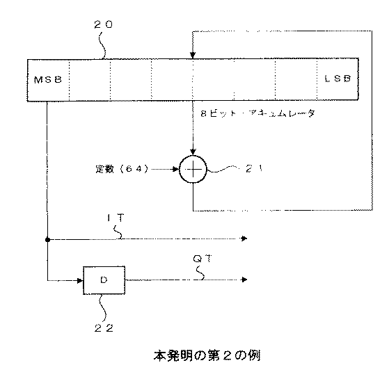
(2)第2の例
この例では、基準信号を図6に示すアキュムレータ20によって発生し、相関値をその基準信号と受信したI・Qデータとの間で検出する。
【0051】
まず、データ処理回路5は、アキュムレータ20から8ビットのデータを出力し、加算回路21で所定の定数をこのデータに加算し、加算結果を再びアキュムレータ20に蓄積する。
【0052】
データ処理回路5は、この加算をA/D変換器16の動作と同期して行い、Iデータに対する基準信号をIT(I Template)としてアキュムレータの最上位ビット(MSB)を出力するように設計される。
【0053】
データ処理回路5は、Iデータに対する基準信号ITを所定の遅延回路(D)22で1サンプリング周期だけ遅らせて、Iデータに対する基準信号からQデータに対する基準信号QT(Q Template)を発生して出力する。
【0054】
本例では、加算回路21への定数の出力値を64に選択し、図7に示すようにそれを累積的に加算して基準信号を発生し、アキュムレータ20と加算回路21の簡単な構成によってそれを実現している。特に、この定数を変えることにより、異なる周波数の基準信号を簡単に発生することができる。
【0055】
GSM規格のデジタル移動電話装置では、ビットレートが約271kbpsであり、周波数制御チャンネルの信号の周波数はそれの1/4の67.7kHzになる。この64の定数を累積的に加算すると、基準信号は67.7kHzの周波数で発生される。
【0056】
しかし実際には、端末1の内部クロックが基地局に対してずれた周波数である場合がある。この時はたとえ64を累積的に加算しても加算周期が基地局と異なるため、発生される基準信号周波数は67.7kHzからずれてしまう。そうなると、端末1は周波数制御チャンネルを明確に検出できない。そこで本例では、所定時間経過しても周波数制御チャンネルの信号が検出できないとき、CPU8がアキュムレータ20に累積的に加算すべき定数を変更する。この際、CPU8はアキュムレータ20の内容を初期化してもよいし、しなくともよい。
【0057】
例えばCPU8が定数の値を64から63に変更すると、アキュムレータ20の最上位ビットの変化が64の場合よりも少し遅れるので、基準信号の繰り返し周期がもとの周期の1/64だけ遅れることとなる。
【0058】
よって端末1は、定数を変えることにより基準信号の周波数を容易に変えることができるので、もし内部クロックに周波数ずれがあっても周波数制御チャンネルの信号を検出できる。さらに周波数ずれそのものも上記定数に基づいて検出できる。
【0059】
ちなみに定数を64から63に変更すると、基準信号の周波数は、271/64=4.2kHzだけ変わる。
【0060】
なお、周波数制御チャンネルの検出精度は、(3)式の閾値を変えて変えることができる。閾値を減らすと、周波数制御チャンネルを発見できる可能性が増し、内部クロックに大きな周波数誤差をあっても周波数制御チャンネルを検出可能となる。ただし、そうすると、周波数制御チャンネルの信号のタイミング以外でも周波数制御チャンネルの信号が到達していると判断されることがあり、検出精度は低下する。
【0061】
これに対し、本例のように相関値を基準信号の周波数の切換によって検出すると、閾値をそれほど下げなくても周波数制御チャンネルの信号を検出できるので、周波数制御チャンネルの検出可能性と検出精度を共に高めることができる。本例でも前の例と同様に、基準信号と受信したI・Qデータとの間で(1)−(3)式の計算を行うことにより、周波数制御チャンネルを検出している。
【0062】
図6に示す構成によれば、定数を累積的に加算して基準信号を発生することにより、第1の例で得られた効果と類似の効果が得られ、この定数を変えることにより、たとえ内部のクロックの周波数がずれていても周波数制御チャンネルを確実に検出できる。
【0063】
(3)第3の例
第2の例において、累積的に加算する定数を変えることにより基準信号の周波数を切り替える場合、定数を変えて何度もスキャン動作を繰り返すことにより、結局周波数制御チャンネルの検出に多くの時間がかかるという欠点がある。
【0064】
図8に示す第3例では、位相相関器25A,25B,25Cは各々値が異なる定数を累積的に加算している。すなわち、これらは周波数が異なる基準信号を同時に別々に発生している。この場合、相関器25A,25B,25Cは、各々受信信号であるI・Qデータと各基準信号との間で(1)式の計算を行う。
【0065】
判定回路26は、相関器25A,25B,25Cから各々出力された(1)式の計算結果に基づいて(2)(3)式の計算を行い、周波数が異なる3つの基準信号を同時に使用して周波数制御チャンネルを検出するので、短時間で検出を行える。
【0066】
判定回路26はまた、検出結果をCPU8に出力し、フレーム同期を行い、25A,25B,25Cのどの相関器から周波数制御チャンネル検出結果が得られるのかを検出する。すなわち、最も大きい相関値を与える相関器を検出する。
【0067】
このように、端末1は周波数制御チャンネル検出をまず検出して周波数誤差を大まかに検出するので、次に行う周波数誤差検出の精度を高めることができる。この周波数誤差検出は、複素平面上のI・Qデータの位相変化を検出することである。この場合、データ処理回路5はまず、周波数制御チャンネル検出結果から得られる値に基づいてI・Qデータの値を修正し、I・Qデータの位相をこの周波数誤差の分だけ回転させる。その後、周波数誤差検出処理を行う。
【0068】
本例によれば、複数の相関器のうちどの相関器の出力が大きいかを調べることにより、大体のクロックの周波数の誤差の値を推定できる。この推定値を次の処理に反映させれば、推定せずに直接周波数誤差を検出する場合に比べて検出精度を高めることができる。図8に示す構成によれば、周波数が異なる並列の複数の基準信号を同時に用いる相関値検出によって周波数制御チャンネルを短時間で検出できるだけでなく、第2の例によって得られる効果をも与えることができる。
【0069】
(4)第4の例
この例では、図9に示すフローチャートを実行して、所定の定数を累積的に加算することによって基準信号を発生し、この基準信号を用いて周波数制御チャンネルを検出する。
【0070】
データ処理回路5は、ステップSP2において、サンプル数および累積的加算を計数するカウンタを0にリセットする。そして定数を64に設定する。これにより、相関関係を検出するのに必要な変数が初期化される。
【0071】
ステップSP3においては、データ処理回路5は受信データのI・Q成分を計算して入力する。次のステップSP4では、データ処理回路5は累積加算値に定数64を加算し、累積加算値の最上位ビットを出力することによって1データに関する基準信号を出力する。そしてステップSP5では、(1)(2)式が計算される。ステップSP6では、受信したI・Qデータならびに相関値の電力が計算される。
【0072】
ステップSP7では(3)式の左側と右側の値を各々計算し、ステップSP8ではその計算結果を判断する。すなわち、(3)式から肯定的結果が得られたかどうかを見る。ステップSP8で否定的結果が得られた場合、データ処理回路5はステップSP9でサンプル数を表すカウンタの計数値を初期化し、ステップSP3に戻る。
【0073】
こうしてデータ処理回路5は、ステップSP3−SP4−SP5−SP6−SP7−SP8−SP9−SP3の処理を繰り返し、(3)式を満足するI・Qデータが入力されると、ステップSP10に進む。
【0074】
ここでデータ処理回路5はカウント値をインクリメントし、ステップSP11でカウント値が所定値Nに達したかどうかを判断し、計算結果が(3)式を満たす入力データがあったかどうかを決定する。
【0075】
この決定が否定的結果の場合はステップSP3に戻り、肯定的結果の場合は周波数制御チャンネルが検出されたと判断してステップSP12に進み処理を終了する。
【0076】
図9に示すフローチャートによれば、たとえ基準信号がソフトウエアにより発生されても、他の例と同じ効果を得ることができる。
【0077】
(5)その他の例
上述の例は、定数として64を累積加算する例を述べたものであるが、本発明はそれに限られることなく、例えばI・Qデータのサンプリング周波数が2倍の場合にはこの定数を半分の値の32に設定すれば良い。
【0078】
また、アキュムレータ20内のビット数を増加することにより、周波数可変ステップをより細かくして基準信号の周波数変化を細かく行うことができ、これによって周波数誤差が小さな値であってもそれを減少されることが可能となる。
【0079】
また、上述の例ではQデータに対応する基準信号をIデータに対する基準信号から遅延させて発生させる場合について述べたが、本発明はそれに限定されるものではなく、Qデータに対応する基準信号は、例えば定数を32に設定してQデータのサンプリング周波数を倍にする場合、Iデータに対応する基準信号を2ビットだけ遅らせて発生させても良い。
【0080】
更に、I・Qデータに対する基準信号は、各々別々にアキュムレータを設けて定数を別々に累積加算することにより、別々に発生しても良い。この場合、初期値としてI・Qデータの位相差分のオフセット値をアキュムレータ20に設定することも可能である。
【0081】
また、上述の例では、(3)式を所定回数以上連続して満足した場合に周波数制御チャンネルが検出されたと判断する場合について述べたが、本発明はこれに限らず、必要に応じて上記基準を緩和しても良い。例えば、受信信号電力が所定の連続回数の全てに渡って基準値を上回ったときに周波数制御チャンネルを検出したとするだけでなく、そのうち回数は基準を下回ってもよいことにしてもよい。
【0082】
また、上述の例では、直交検波によって得られたベースバンド信号をI・Qデータに変換することにより相関値を検出する場合について述べたが、本発明はこれに限定されることなく、中間周波信号を遅延回路に入力してベースバンド信号を得るような遅延検波を用いる場合にも広く適用することができる。
【0083】
また、上述の例では、受信電力からの減算により相関値を正規化する場合について述べたが、除算により正規化してもよい。
【0084】
また、上述の例では、本発明をデジタル移動電話装置に適用する場合について述べたが、他の、所定の周期で挿入された同期信号を参照して無線送信されたデータストリームを復調する無線受信機にも広く適用可能である。
【0085】
【発明の効果】
本発明によれはベースバンドに変換されたI・Q信号をデジタル値に変換した後、それと所定の基準信号との相関関係を検出することによって求まる値に基づいて周波数制御チャンネルの信号を検出するので、フェージングやノイズの影響を受けずに周波数制御チャンネルの同期信号を容易に確実に検出することができる利益がある。
【図面の簡単な説明】
【図1】FCCH(周波数制御チャンネル)の送信を説明するための波形図である。
【図2】本発明の第1の例によるデジタル移動電話の端末を示すブロック図である。
【図3】図2の端末の受信系を詳細に示すブロック図である。
【図4】図3の受信系の動作を示すグラフである。
【図5】FCCH検出用の基準パターンを示す表図である。
【図6】本発明の第2の例を示すブロック図である。
【図7】図6の装置の動作を示す表図である。
【図8】本発明の第3の例を示すブロック図である。
【図9】本発明の第4の例を説明するためのフローチャートである。
【符号の説明】
1 無線受信機、3,10 増幅回路、4 RF処理回路、5 データ処理回路、6 音声処理回路、7 スピーカ、8 CPU、9 マイクロホン、11 ROM、12 表示キー入力部、13 RAM、15 検波回路、16A/Dコンバータ、17 復号デジタル・シグナル・プロセッサ、20 アキュムレータ、21 加算回路、25A,25B,25C 位相相関器[0001]
BACKGROUND OF THE INVENTION
The present invention relates to a radio receiver and a radio reception method, and is suitable for use in, for example, a digital mobile telephone apparatus that encodes and transmits audio signals.
[0002]
[Background Art and Problems to be Solved by the Invention]
Conventionally, in a digital cellular system having a digital mobile telephone device, a plurality of terminal devices have simultaneously used one channel by using a time division multiplexing method using an encoded voice signal.
More specifically, when the radio wave arrives, the terminal scans all 124 channels in order and selects the channel with the strongest electric field strength.
[0003]
The terminal detects the control channel assigned to each area and receives it. In this system, there are 124 channels available per cell. The position of the control channel is not fixed to a specific channel among the 124 channels. Therefore, the system apparatus sequentially scans all 124 channels, rearranges them in the order of the electric field strength, and searches for a frequency control channel (FCCH) from the rearranged list. The searched control channel is used to form time slots and transmit various information. In this digital cellular system, information is transmitted from each terminal to the base station, information is transmitted between adjacent base stations, and the base station Used to call other terminals.
[0004]
The terminal detects a signal periodically inserted into this control channel. Based on this signal, the operation timing is adjusted, and at the same time, the approximate position of the time slot where the necessary information exists is detected.
[0005]
The signal of the frequency control channel is synchronized with a bit pattern in which a value of “0” continues for a predetermined number of bits when it is decoded by a digital mobile telephone terminal, and this data is differentially encoded. After GMSK (Gaussian filtered minimum shift keying) modulation, it is transmitted. As shown in FIG. 1, the signal of the frequency control channel is represented as a composite of an I signal and a Q signal obtained by modulating information into a sine wave having a phase difference of 90 °. This signal is offset by +67.7 kHz from the carrier frequency.
[0006]
The digital mobile telephone apparatus extracts the signal component of the frequency control channel from the received signal by a band pass filter, detects its timing, and synchronizes the entire operation based on the detected timing. When the signal component of the frequency control channel is extracted by the bandpass filter as described above, the detection accuracy becomes higher as the bandwidth of the bandpass filter is narrower. However, if the bandwidth is narrowed, the response characteristics will deteriorate.
[0007]
Since the duration of the signal of the frequency control channel of the GSM digital cellular system is as short as 550 μs, it becomes difficult to detect the frequency control channel if the response characteristic of the bandpass filter deteriorates.
[0008]
Further, in the digital mobile telephone device, the frequency may be shifted due to the Doppler shift, and data other than the frequency control channel signal may have the same frequency as the frequency control channel signal. Therefore, when a bandpass filter is used, the timing of the frequency control channel signal may be detected incorrectly or not at all. In such a case, since it is attempted to detect again the signal of the frequency control channel that is repeatedly transmitted at a predetermined cycle, it takes time until a call can be made.
[0009]
There is also a method for detecting a frequency control channel from a decoded data stream. The frequency control channel can be detected by correlation detection using the continuity of the decoded data stream or pattern matching by comparison with a predetermined pattern. However, even if this method is used, many decoding errors occur due to Doppler shift, noise, and fading.
[0010]
In particular, regarding the noise level, Eb / No (Eb is communication energy per bit. No is noise power density. Eb / No is a general numerical value representing the state of the communication medium.) Is deteriorated to 10 dB or less. There is. In this case, the error rate of the decoded data stream becomes high, and the frequency control channel cannot be detected correctly.
[0011]
In addition to this, quadrature detection is performed on the received signals to generate I / Q signals, and the correlation function of I / Q is detected by utilizing the fact that these signals have information components with a phase shifted by 90 °. A method for detecting the frequency control channel is also conceivable. However, when there are many repetitive patterns or the like in signal components other than the frequency control channel, since there is a high correlation between them, they are often erroneously detected as signals of the frequency control channel.
In view of the above points, an object of the present invention is to provide a radio receiver and a radio reception method capable of easily and reliably detecting the synchronization signal of the frequency control channel.
[0012]
[Means for Solving the Problems]
The radio receiver of the present invention includes a demodulating means for demodulating a baseband signal from a received signal, a decoding means for decoding a data signal from an output signal of the demodulating means, and a reference for generating a reference signal based on the output signal of the decoding means Signal generating means, and correlation value detecting means adapted to detect a complex correlation value between the data signal and the reference signal, and detecting a synchronization signal based on the detected complex correlation value In the wireless receiver that decodes the received signal based on the synchronization signal of the predetermined pattern that is decoded based on the detected synchronization signal and inserted in a predetermined cycle, the detected correlation value power is PCORR, The received signal power is PREC, The threshold is THWhen
PREC-PCORR× TH≦ 0
Is continuously established over a predetermined sampling periodSometimes it is determined that a signal of the frequency control channel has been detected, and frame synchronization control is performed.It is what I did.
[0013]
According to the present invention, after the I / Q signal converted into the baseband is converted into a digital value, the signal of the frequency control channel is converted based on the value obtained by detecting the correlation between the digital signal and the predetermined reference signal. Since it is detected, the synchronization signal of the frequency control channel can be easily and reliably detected without being affected by fading or noise.
[0014]
DETAILED DESCRIPTION OF THE INVENTION
Hereinafter, embodiments of the present invention will be described with reference to the drawings.
[0015]
(1) First example
FIG. 2 is a block diagram showing a digital mobile telephone apparatus terminal according to this example. In FIG. 2, a
[0016]
The
[0017]
The
[0018]
The
[0019]
The
[0020]
In addition to these processes, the
[0021]
The
[0022]
On the other hand, the CPU 8 receives predetermined information transmitted from the base station based on the decoded data, switches the frequency of the local oscillation signal based on the reception result, and the transmission / reception frequency is switched to the predetermined communication channel. 1 can transmit and receive an audio signal by selecting a predetermined channel.
[0023]
Further, the transmission unit of the
[0024]
The
[0025]
At this time, the
[0026]
The CPU 8 secures a work area in the RAM 13 and executes a control program stored in the ROM 11, thereby outputting a control code to each circuit as necessary to control the operation of the entire apparatus. For example, when the operator presses a predetermined key on the display key input unit 12, a call signal is transmitted to the base station in response to this operation, and when a call signal is received from the base station, the reception channel and the like are switched.
[0027]
The
[0028]
The audio decoding digital signal processor (DSP) 6 comprises a digital signal processor for processing audio data, and decompresses the signal from the
[0029]
First, before the above process, the
[0030]
Specifically, the reception of the frequency control channel is as follows. First, the A / D converter 16 sequentially samples the I / Q signals at a predetermined cycle and generates 8-bit I / Q data. Here, the transmitted I / Q signals forming the frequency control channel have information components with phases shifted by 90 °.
[0031]
As shown in FIG. 4, when the I / Q signal obtained by decoding the received frequency control channel signal is plotted on the complex plane represented by the reference I / Q axes, the received frequency control is obtained. The channel signal rotates counterclockwise by π / 2 radians on the complex plane to form a circular locus. However, if the received frequency control channel signal is affected by fading or noise, the amplitude / phase of the I / Q signal changes according to the amount thereof, and the circle locus for the I / Q data is distorted.
[0032]
Further, when the internal clock is not synchronized with the received frequency control channel signal in the
[0033]
In order to correctly detect the frequency control channel burst signal in such a frequency control channel, a waveform similar to the frequency control channel signal is generated inside the receiver, and this is used as a reference waveform (template) to correlate with the received signal. To calculate the frequency control channel signal.
[0034]
The template has the same waveform as the ideal frequency control channel signal reception waveform when there is no influence of fading or noise. This template is considered to be a signal having a 4-bit period, and as shown in FIG.0~ TThree) Can be prepared in advance.
[0035]
The
[0036]
Where the mth sample for each of the I and Q data is Im・ QmAnd the mth template value and its complex conjugate are each Tim・ TqmIt expresses. The length of the correlation value is n, and the intermediate value of the calculation is CmIt expresses. Where Tim・ TqmThe value of is −1 or +1. The length n of the correlation value represents the number of data for the correlation calculation. At this time, the
[0037]
[Expression 1]
[0038]
The
[Expression 2]
Then, whether or not the signal of the frequency control channel can be detected is determined by the true / false determination of the following equation (3).
[0040]
The detected correlation power is PCORR, Received signal power is PREC, Threshold is THWhen
[Equation 3]
PREC-PCORR × TH≦ 0 (3)
It is assumed that the signal of the frequency control channel is detected when
[0041]
Where PCORRRepresents the square of the correlation detection result, and can be obtained by the following equation (4).
[0042]
[Expression 4]
PCORR= | CORRK|2 (4)
[0043]
PRECRepresents the power of the received signal and can be represented by equation (5).
[0044]
[Equation 5]
PREC= Im 2+ Qm 2 (5)
[0045]
The determination expressed by the expression (3) is performed for each sample, and if the expression (3) is satisfied over a predetermined number of sampling periods, the
[0046]
Correlation value C between IQ data converted to baseband and templateORRKIncreases not only when the signal of the frequency control channel is received but also when the amplitude of the I · Q signal increases with the increase of the received signal level.
[0047]
Therefore, the
[0048]
Further, in this case, the
[0049]
According to this example, after the I / Q signal converted into the baseband is converted into a digital value, the signal of the frequency control channel is detected based on the value obtained by detecting the correlation between the digital signal and the predetermined reference signal. Therefore, the frequency control channel can be easily and reliably detected without being affected by fading or noise.
[0050]
(2) Second example
In this example, a reference signal is generated by the
[0051]
First, the
[0052]
The
[0053]
The
[0054]
In this example, the output value of the constant to the
[0055]
In the digital mobile telephone apparatus of the GSM standard, the bit rate is about 271 kbps, and the frequency of the signal of the frequency control channel is 1/4 of that, 67.7 kHz. When the 64 constants are cumulatively added, the reference signal is generated at a frequency of 67.7 kHz.
[0056]
However, in practice, the internal clock of the
[0057]
For example, when the CPU 8 changes the value of the constant from 64 to 63, the change of the most significant bit of the
[0058]
Therefore, since the
[0059]
Incidentally, if the constant is changed from 64 to 63, the frequency of the reference signal changes by 271/64 = 4.2 kHz.
[0060]
The detection accuracy of the frequency control channel can be changed by changing the threshold value of the equation (3). Decreasing the threshold increases the possibility of finding the frequency control channel, and the frequency control channel can be detected even if there is a large frequency error in the internal clock. However, in that case, it may be determined that the signal of the frequency control channel has arrived at other than the timing of the signal of the frequency control channel, and the detection accuracy is lowered.
[0061]
On the other hand, if the correlation value is detected by switching the frequency of the reference signal as in this example, the signal of the frequency control channel can be detected without lowering the threshold so much, so the detectability and detection accuracy of the frequency control channel are improved. Both can be enhanced. In this example, similarly to the previous example, the frequency control channel is detected by calculating the equations (1) to (3) between the reference signal and the received I / Q data.
[0062]
According to the configuration shown in FIG. 6, by generating a reference signal by cumulatively adding constants, an effect similar to the effect obtained in the first example is obtained. By changing this constant, for example, Even if the frequency of the internal clock is shifted, the frequency control channel can be reliably detected.
[0063]
(3) Third example
In the second example, when the frequency of the reference signal is switched by changing the constant to be cumulatively added, it takes a lot of time to detect the frequency control channel after changing the constant and repeating the scanning operation many times. There is a drawback.
[0064]
In the third example shown in FIG. 8, the phase correlators 25A, 25B, and 25C cumulatively add constants having different values. That is, they generate reference signals having different frequencies at the same time. In this case, the correlators 25A, 25B, and 25C perform the calculation of equation (1) between the I / Q data that is the received signal and each reference signal.
[0065]
The
[0066]
The
[0067]
In this way, since the
[0068]
According to this example, it is possible to estimate an error value of an approximate clock frequency by examining which correlator output of the plurality of correlators is large. If this estimated value is reflected in the next processing, the detection accuracy can be improved as compared with the case where the frequency error is directly detected without estimation. According to the configuration shown in FIG. 8, not only the frequency control channel can be detected in a short time by the correlation value detection using a plurality of parallel reference signals having different frequencies simultaneously, but also the effect obtained by the second example can be provided. it can.
[0069]
(4) Fourth example
In this example, the flowchart shown in FIG. 9 is executed, a reference signal is generated by cumulatively adding a predetermined constant, and a frequency control channel is detected using this reference signal.
[0070]
In step SP2, the
[0071]
In step SP3, the
[0072]
In step SP7, the values on the left and right sides of equation (3) are calculated, and in step SP8, the calculation result is determined. That is, it is checked whether a positive result is obtained from the expression (3). If a negative result is obtained in step SP8, the
[0073]
In this way, the
[0074]
Here, the
[0075]
If this determination is negative, the process returns to step SP3. If the determination is positive, it is determined that the frequency control channel has been detected, and the process proceeds to step SP12 to end the process.
[0076]
According to the flowchart shown in FIG. 9, even if the reference signal is generated by software, the same effects as those of the other examples can be obtained.
[0077]
(5) Other examples
The above example describes an example of cumulatively adding 64 as a constant. However, the present invention is not limited to this. For example, when the sampling frequency of I / Q data is doubled, this constant is reduced to half. A value of 32 may be set.
[0078]
Further, by increasing the number of bits in the
[0079]
In the above example, the case where the reference signal corresponding to the Q data is generated after being delayed from the reference signal for the I data has been described. However, the present invention is not limited thereto, and the reference signal corresponding to the Q data is For example, when the constant is set to 32 and the sampling frequency of Q data is doubled, the reference signal corresponding to I data may be generated with a delay of 2 bits.
[0080]
Further, the reference signals for the I / Q data may be generated separately by separately providing accumulators and separately accumulating constants separately. In this case, an offset value of the phase difference between the I and Q data can be set in the
[0081]
Further, in the above-described example, the case where it is determined that the frequency control channel is detected when the expression (3) is continuously satisfied a predetermined number of times or more has been described. Standards may be relaxed. For example, not only the frequency control channel is detected when the received signal power exceeds the reference value over a predetermined number of consecutive times, but the number of times may be less than the reference.
[0082]
In the above example, the case where the correlation value is detected by converting the baseband signal obtained by the quadrature detection into the I / Q data has been described. However, the present invention is not limited to this, and the intermediate frequency The present invention can be widely applied to the case of using delay detection in which a signal is input to a delay circuit to obtain a baseband signal.
[0083]
In the above example, the case where the correlation value is normalized by subtraction from the received power has been described. However, normalization may be performed by division.
[0084]
In the above-described example, the case where the present invention is applied to a digital mobile telephone device has been described. However, other wireless reception for demodulating a data stream wirelessly transmitted with reference to a synchronization signal inserted at a predetermined period is described. Widely applicable to machines.
[0085]
【The invention's effect】
According to the present invention, after the I / Q signal converted into the baseband is converted into a digital value, the signal of the frequency control channel is detected based on the value obtained by detecting the correlation between the digital signal and the predetermined reference signal. Therefore, there is an advantage that the synchronization signal of the frequency control channel can be easily and reliably detected without being affected by fading or noise.
[Brief description of the drawings]
FIG. 1 is a waveform diagram for explaining transmission of an FCCH (frequency control channel).
FIG. 2 is a block diagram showing a digital mobile telephone terminal according to the first example of the present invention;
FIG. 3 is a block diagram showing in detail a reception system of the terminal in FIG. 2;
4 is a graph showing the operation of the reception system in FIG. 3;
FIG. 5 is a table showing a reference pattern for FCCH detection.
FIG. 6 is a block diagram showing a second example of the present invention.
7 is a table showing the operation of the apparatus of FIG.
FIG. 8 is a block diagram showing a third example of the present invention.
FIG. 9 is a flowchart for explaining a fourth example of the present invention.
[Explanation of symbols]
DESCRIPTION OF
Claims (22)
前記復調手段の出力信号からデータ信号を復号する復号手段と、
前記復号手段の出力信号に基づいて基準信号を発生する基準信号発生手段と、
前記データ信号と前記基準信号との間の複素相関値を検出するようにされた相関値検出手段とを有し、
前記検出された複素相関値に基づいて同期信号を検出し、検出した前記同期信号に基づいて前記復号を行い所定周期で挿入された所定パターンの同期信号に基づいて、受信信号を復号するようにした無線受信機において、
検出された相関値電力をPCORR、受信信号電力をPREC、閾値をTHとしたとき
PREC−PCORR×TH≦0
が所定のサンプリング期間にわたって連続的に成立するときに、周波数制御チャンネルの信号が検出されたと判断してフレーム同期制御を行うようにしたことを特徴とする無線受信機。Demodulation means for demodulating the baseband signal from the received signal;
Decoding means for decoding a data signal from the output signal of the demodulation means;
Reference signal generating means for generating a reference signal based on an output signal of the decoding means;
Correlation value detection means adapted to detect a complex correlation value between the data signal and the reference signal;
A synchronization signal is detected based on the detected complex correlation value, the decoding is performed based on the detected synchronization signal, and the received signal is decoded based on the synchronization signal having a predetermined pattern inserted at a predetermined period. Wireless receiver
When the detected correlation value power is P CORR , the received signal power is P REC , and the threshold is T H , P REC −P CORR × T H ≦ 0
A radio receiver characterized in that when the signal is continuously established over a predetermined sampling period, it is determined that a signal of a frequency control channel has been detected and frame synchronization control is performed .
加算結果を累積しておくレジスタ手段とからなることを特徴とする無線受信機。2. The radio receiver according to claim 1, wherein the reference signal generating means includes an adding means for adding a predetermined constant;
A radio receiver comprising register means for accumulating addition results.
前記復調ステップの出力信号からデータ信号を復号する復号ステップと、
前記復号ステップの出力信号に基づいて基準信号を発生する基準信号発生ステップと、
前記データ信号と前記基準信号との間の複素相関値を検出するようにされた相関値検出ステップとからなり、
前記検出された複素相関値に基づいて同期信号を検出し、検出した前記同期信号に基づいて前記復号を行い所定周期で挿入された所定パターンの同期信号に基づいて、受信信号を復号するようにした無線受信方法において、
検出された相関値電力をPCORR、受信信号電力をPREC、閾値をTHとしたとき、
PREC−PCORR×TH≦0
が所定サンプリング期間にわたって連続的に成立するときに、周波数制御チャンネルの信号が検出されたと判断してフレーム同期制御を行うようにしたことを特徴とする無線受信方法。A demodulation step of demodulating the baseband signal from the received signal;
A decoding step of decoding a data signal from the output signal of the demodulation step;
A reference signal generating step for generating a reference signal based on the output signal of the decoding step;
A correlation value detecting step adapted to detect a complex correlation value between the data signal and the reference signal;
A synchronization signal is detected based on the detected complex correlation value, the decoding is performed based on the detected synchronization signal, and the received signal is decoded based on the synchronization signal having a predetermined pattern inserted at a predetermined period. In the received wireless reception method,
When the detected correlation value power P CORR, the received signal power P REC, the threshold was set to T H,
P REC −P CORR × T H ≦ 0
A radio reception method characterized in that when the signal is continuously established over a predetermined sampling period, it is determined that a signal of the frequency control channel is detected and frame synchronization control is performed .
所定の定数を加算する加算ステップと、
加算結果を累積しておくレジスタステップとからなることを特徴とする無線受信方法。13. The wireless reception method according to claim 12, wherein the reference signal generation step includes:
An addition step of adding a predetermined constant;
A wireless reception method comprising: a register step for accumulating addition results.
Priority Applications (1)
| Application Number | Priority Date | Filing Date | Title |
|---|---|---|---|
| JP07805697A JP3718577B2 (en) | 1997-03-28 | 1997-03-28 | Radio receiver and radio reception method |
Applications Claiming Priority (1)
| Application Number | Priority Date | Filing Date | Title |
|---|---|---|---|
| JP07805697A JP3718577B2 (en) | 1997-03-28 | 1997-03-28 | Radio receiver and radio reception method |
Publications (2)
| Publication Number | Publication Date |
|---|---|
| JPH10276233A JPH10276233A (en) | 1998-10-13 |
| JP3718577B2 true JP3718577B2 (en) | 2005-11-24 |
Family
ID=13651206
Family Applications (1)
| Application Number | Title | Priority Date | Filing Date |
|---|---|---|---|
| JP07805697A Expired - Fee Related JP3718577B2 (en) | 1997-03-28 | 1997-03-28 | Radio receiver and radio reception method |
Country Status (1)
| Country | Link |
|---|---|
| JP (1) | JP3718577B2 (en) |
Cited By (1)
| Publication number | Priority date | Publication date | Assignee | Title |
|---|---|---|---|---|
| KR101667886B1 (en) * | 2015-07-28 | 2016-10-28 | 엘에스산전 주식회사 | Data control system |
Family Cites Families (8)
| Publication number | Priority date | Publication date | Assignee | Title |
|---|---|---|---|---|
| JP2744076B2 (en) * | 1989-08-09 | 1998-04-28 | 株式会社日立製作所 | Frame synchronization detection circuit |
| JP2856480B2 (en) * | 1990-02-27 | 1999-02-10 | 日本電気株式会社 | Signal detection system for signal synchronization |
| US5371765A (en) * | 1992-07-10 | 1994-12-06 | Hewlett-Packard Company | Binary phase accumulator for decimal frequency synthesis |
| US5408504A (en) * | 1992-12-30 | 1995-04-18 | Nokia Mobile Phones | Symbol and frame synchronization in a TDMA system |
| JP3402375B2 (en) * | 1993-01-28 | 2003-05-06 | 株式会社アドバンテスト | DQPSK modulation signal evaluation device |
| JPH07297870A (en) * | 1994-04-26 | 1995-11-10 | Matsushita Electric Ind Co Ltd | Tdma data receiver |
| JPH0823361A (en) * | 1994-07-06 | 1996-01-23 | Matsushita Electric Ind Co Ltd | Tdma data receiver |
| JP3121995B2 (en) * | 1994-10-24 | 2001-01-09 | 松下電器産業株式会社 | Synchronizer |
-
1997
- 1997-03-28 JP JP07805697A patent/JP3718577B2/en not_active Expired - Fee Related
Cited By (2)
| Publication number | Priority date | Publication date | Assignee | Title |
|---|---|---|---|---|
| KR101667886B1 (en) * | 2015-07-28 | 2016-10-28 | 엘에스산전 주식회사 | Data control system |
| US9948105B2 (en) | 2015-07-28 | 2018-04-17 | Lsis Co., Ltd. | Data control system |
Also Published As
| Publication number | Publication date |
|---|---|
| JPH10276233A (en) | 1998-10-13 |
Similar Documents
| Publication | Publication Date | Title |
|---|---|---|
| JP3723653B2 (en) | Digital mobile phone equipment | |
| JP3301555B2 (en) | Wireless receiver | |
| US5182749A (en) | Receiver for recovering data in a forward and reverse direction in time | |
| WO2006036009A1 (en) | Mobile wireless communication apparatus, wireless communication apparatus and communication processing method | |
| JP2003046418A (en) | Diversity receiver | |
| US6301684B1 (en) | Data decoding apparatus and method for decoding convolution-coded input data | |
| JPH09214417A (en) | Transmitter and transmission method | |
| EP0958686B1 (en) | Demodulation with separate branches for phase and amplitude | |
| US5905764A (en) | Radio receiver | |
| JP3703589B2 (en) | Radio receiving apparatus and radio receiving method | |
| US6038270A (en) | Radio receiver apparatus and radio receiving method | |
| JP3649542B2 (en) | Nonlinear signal correlator and method thereof | |
| JP3624547B2 (en) | Burst signal receiving method and apparatus | |
| JP3718577B2 (en) | Radio receiver and radio reception method | |
| JP2004513567A (en) | Decision feedback loop apparatus and method for performing channel estimation and derotation using burst pilot bits | |
| JP3433822B2 (en) | Wireless device | |
| US7620122B1 (en) | Communication apparatus including a demodulator having a tone detection mechanism | |
| JPH09298492A (en) | Afc circuit | |
| JPH10256969A (en) | Radio base station equipment | |
| JP2005130296A (en) | Receiver and receiving method of call signal | |
| JPH08163012A (en) | Transmission line estimate circuit | |
| JP2001274725A (en) | Agc circuit and synchronization capture method | |
| JPH10233722A (en) | Diversity receiver |
Legal Events
| Date | Code | Title | Description |
|---|---|---|---|
| A977 | Report on retrieval |
Free format text: JAPANESE INTERMEDIATE CODE: A971007 Effective date: 20041209 |
|
| A131 | Notification of reasons for refusal |
Free format text: JAPANESE INTERMEDIATE CODE: A131 Effective date: 20041214 |
|
| A521 | Written amendment |
Free format text: JAPANESE INTERMEDIATE CODE: A523 Effective date: 20050223 |
|
| A131 | Notification of reasons for refusal |
Free format text: JAPANESE INTERMEDIATE CODE: A131 Effective date: 20050705 |
|
| A521 | Written amendment |
Free format text: JAPANESE INTERMEDIATE CODE: A523 Effective date: 20050805 |
|
| TRDD | Decision of grant or rejection written | ||
| A01 | Written decision to grant a patent or to grant a registration (utility model) |
Free format text: JAPANESE INTERMEDIATE CODE: A01 Effective date: 20050830 |
|
| A61 | First payment of annual fees (during grant procedure) |
Free format text: JAPANESE INTERMEDIATE CODE: A61 Effective date: 20050905 |
|
| R150 | Certificate of patent or registration of utility model |
Free format text: JAPANESE INTERMEDIATE CODE: R150 |
|
| FPAY | Renewal fee payment (event date is renewal date of database) |
Free format text: PAYMENT UNTIL: 20080909 Year of fee payment: 3 |
|
| FPAY | Renewal fee payment (event date is renewal date of database) |
Free format text: PAYMENT UNTIL: 20090909 Year of fee payment: 4 |
|
| LAPS | Cancellation because of no payment of annual fees |