JP3708637B2 - Liquid crystal display device - Google Patents
Liquid crystal display device Download PDFInfo
- Publication number
- JP3708637B2 JP3708637B2 JP20537896A JP20537896A JP3708637B2 JP 3708637 B2 JP3708637 B2 JP 3708637B2 JP 20537896 A JP20537896 A JP 20537896A JP 20537896 A JP20537896 A JP 20537896A JP 3708637 B2 JP3708637 B2 JP 3708637B2
- Authority
- JP
- Japan
- Prior art keywords
- shielding film
- bus line
- light shielding
- film
- light
- Prior art date
- Legal status (The legal status is an assumption and is not a legal conclusion. Google has not performed a legal analysis and makes no representation as to the accuracy of the status listed.)
- Expired - Lifetime
Links
- 239000004973 liquid crystal related substance Substances 0.000 title claims description 15
- 239000011159 matrix material Substances 0.000 claims description 16
- 239000003990 capacitor Substances 0.000 claims description 15
- 239000004065 semiconductor Substances 0.000 claims description 14
- 239000010408 film Substances 0.000 description 189
- 239000010410 layer Substances 0.000 description 50
- 238000000034 method Methods 0.000 description 36
- VYPSYNLAJGMNEJ-UHFFFAOYSA-N Silicium dioxide Chemical compound O=[Si]=O VYPSYNLAJGMNEJ-UHFFFAOYSA-N 0.000 description 29
- 229910052814 silicon oxide Inorganic materials 0.000 description 29
- 239000000758 substrate Substances 0.000 description 20
- 229910052581 Si3N4 Inorganic materials 0.000 description 19
- HQVNEWCFYHHQES-UHFFFAOYSA-N silicon nitride Chemical compound N12[Si]34N5[Si]62N3[Si]51N64 HQVNEWCFYHHQES-UHFFFAOYSA-N 0.000 description 19
- 238000000206 photolithography Methods 0.000 description 18
- 238000005268 plasma chemical vapour deposition Methods 0.000 description 17
- 229910052715 tantalum Inorganic materials 0.000 description 17
- GUVRBAGPIYLISA-UHFFFAOYSA-N tantalum atom Chemical compound [Ta] GUVRBAGPIYLISA-UHFFFAOYSA-N 0.000 description 17
- 238000004544 sputter deposition Methods 0.000 description 16
- 239000012212 insulator Substances 0.000 description 12
- 239000011229 interlayer Substances 0.000 description 12
- 238000004519 manufacturing process Methods 0.000 description 11
- 229920001721 polyimide Polymers 0.000 description 7
- 239000012535 impurity Substances 0.000 description 6
- RTAQQCXQSZGOHL-UHFFFAOYSA-N Titanium Chemical compound [Ti] RTAQQCXQSZGOHL-UHFFFAOYSA-N 0.000 description 5
- 229910052782 aluminium Inorganic materials 0.000 description 5
- XAGFODPZIPBFFR-UHFFFAOYSA-N aluminium Chemical compound [Al] XAGFODPZIPBFFR-UHFFFAOYSA-N 0.000 description 5
- 238000005224 laser annealing Methods 0.000 description 5
- 229910052719 titanium Inorganic materials 0.000 description 5
- 239000010936 titanium Substances 0.000 description 5
- 229910021417 amorphous silicon Inorganic materials 0.000 description 4
- 238000000137 annealing Methods 0.000 description 4
- AMGQUBHHOARCQH-UHFFFAOYSA-N indium;oxotin Chemical compound [In].[Sn]=O AMGQUBHHOARCQH-UHFFFAOYSA-N 0.000 description 4
- 150000002500 ions Chemical class 0.000 description 4
- 229910001069 Ti alloy Inorganic materials 0.000 description 3
- UQZIWOQVLUASCR-UHFFFAOYSA-N alumane;titanium Chemical compound [AlH3].[Ti] UQZIWOQVLUASCR-UHFFFAOYSA-N 0.000 description 3
- 238000005530 etching Methods 0.000 description 3
- 238000004518 low pressure chemical vapour deposition Methods 0.000 description 3
- 238000001953 recrystallisation Methods 0.000 description 3
- 229910000838 Al alloy Inorganic materials 0.000 description 2
- 230000000903 blocking effect Effects 0.000 description 2
- 229910021419 crystalline silicon Inorganic materials 0.000 description 2
- 230000000694 effects Effects 0.000 description 2
- 239000011521 glass Substances 0.000 description 2
- 239000010409 thin film Substances 0.000 description 2
- VYZAMTAEIAYCRO-UHFFFAOYSA-N Chromium Chemical compound [Cr] VYZAMTAEIAYCRO-UHFFFAOYSA-N 0.000 description 1
- XUIMIQQOPSSXEZ-UHFFFAOYSA-N Silicon Chemical compound [Si] XUIMIQQOPSSXEZ-UHFFFAOYSA-N 0.000 description 1
- 230000015556 catabolic process Effects 0.000 description 1
- 229910052804 chromium Inorganic materials 0.000 description 1
- 239000011651 chromium Substances 0.000 description 1
- 238000009792 diffusion process Methods 0.000 description 1
- 230000005684 electric field Effects 0.000 description 1
- 229910010272 inorganic material Inorganic materials 0.000 description 1
- 239000011147 inorganic material Substances 0.000 description 1
- 238000009413 insulation Methods 0.000 description 1
- 230000010354 integration Effects 0.000 description 1
- 230000014759 maintenance of location Effects 0.000 description 1
- 239000000463 material Substances 0.000 description 1
- 229910052751 metal Inorganic materials 0.000 description 1
- 239000002184 metal Substances 0.000 description 1
- 230000003071 parasitic effect Effects 0.000 description 1
- 238000000059 patterning Methods 0.000 description 1
- 229910052710 silicon Inorganic materials 0.000 description 1
- 239000010703 silicon Substances 0.000 description 1
- 230000000087 stabilizing effect Effects 0.000 description 1
Images


Classifications
-
- G—PHYSICS
- G02—OPTICS
- G02F—OPTICAL DEVICES OR ARRANGEMENTS FOR THE CONTROL OF LIGHT BY MODIFICATION OF THE OPTICAL PROPERTIES OF THE MEDIA OF THE ELEMENTS INVOLVED THEREIN; NON-LINEAR OPTICS; FREQUENCY-CHANGING OF LIGHT; OPTICAL LOGIC ELEMENTS; OPTICAL ANALOGUE/DIGITAL CONVERTERS
- G02F1/00—Devices or arrangements for the control of the intensity, colour, phase, polarisation or direction of light arriving from an independent light source, e.g. switching, gating or modulating; Non-linear optics
- G02F1/01—Devices or arrangements for the control of the intensity, colour, phase, polarisation or direction of light arriving from an independent light source, e.g. switching, gating or modulating; Non-linear optics for the control of the intensity, phase, polarisation or colour
- G02F1/13—Devices or arrangements for the control of the intensity, colour, phase, polarisation or direction of light arriving from an independent light source, e.g. switching, gating or modulating; Non-linear optics for the control of the intensity, phase, polarisation or colour based on liquid crystals, e.g. single liquid crystal display cells
- G02F1/133—Constructional arrangements; Operation of liquid crystal cells; Circuit arrangements
- G02F1/136—Liquid crystal cells structurally associated with a semi-conducting layer or substrate, e.g. cells forming part of an integrated circuit
- G02F1/1362—Active matrix addressed cells
- G02F1/136209—Light shielding layers, e.g. black matrix, incorporated in the active matrix substrate, e.g. structurally associated with the switching element
-
- H—ELECTRICITY
- H01—ELECTRIC ELEMENTS
- H01L—SEMICONDUCTOR DEVICES NOT COVERED BY CLASS H10
- H01L27/00—Devices consisting of a plurality of semiconductor or other solid-state components formed in or on a common substrate
- H01L27/02—Devices consisting of a plurality of semiconductor or other solid-state components formed in or on a common substrate including semiconductor components specially adapted for rectifying, oscillating, amplifying or switching and having potential barriers; including integrated passive circuit elements having potential barriers
- H01L27/12—Devices consisting of a plurality of semiconductor or other solid-state components formed in or on a common substrate including semiconductor components specially adapted for rectifying, oscillating, amplifying or switching and having potential barriers; including integrated passive circuit elements having potential barriers the substrate being other than a semiconductor body, e.g. an insulating body
- H01L27/1214—Devices consisting of a plurality of semiconductor or other solid-state components formed in or on a common substrate including semiconductor components specially adapted for rectifying, oscillating, amplifying or switching and having potential barriers; including integrated passive circuit elements having potential barriers the substrate being other than a semiconductor body, e.g. an insulating body comprising a plurality of TFTs formed on a non-semiconducting substrate, e.g. driving circuits for AMLCDs
- H01L27/1255—Devices consisting of a plurality of semiconductor or other solid-state components formed in or on a common substrate including semiconductor components specially adapted for rectifying, oscillating, amplifying or switching and having potential barriers; including integrated passive circuit elements having potential barriers the substrate being other than a semiconductor body, e.g. an insulating body comprising a plurality of TFTs formed on a non-semiconducting substrate, e.g. driving circuits for AMLCDs integrated with passive devices, e.g. auxiliary capacitors
Landscapes
- Physics & Mathematics (AREA)
- Engineering & Computer Science (AREA)
- Microelectronics & Electronic Packaging (AREA)
- General Physics & Mathematics (AREA)
- Power Engineering (AREA)
- Nonlinear Science (AREA)
- Computer Hardware Design (AREA)
- Condensed Matter Physics & Semiconductors (AREA)
- Mathematical Physics (AREA)
- Chemical & Material Sciences (AREA)
- Crystallography & Structural Chemistry (AREA)
- Optics & Photonics (AREA)
- Liquid Crystal (AREA)
- Thin Film Transistor (AREA)
Description
【0001】
【発明の属する技術分野】
本発明は一般に液晶表示装置に関し、特に液晶パネルを構成する一対の対向基板のうち、TFT(薄膜トランジスタ)を担持する側の基板の遮光膜の配置に特色を有するものに関する。
【0002】
【従来の技術】
液晶表示装置は投射型もしくは直視型の表示装置として広く使われている。特に、高解像度カラー表示を達成するためには、個々の画素を薄膜トランジスタ(TFT)により駆動する、いわゆるアクティブマトリクス方式の液晶表示装置が適している。アクティブマトリクス駆動方式を使うことにより、単純マトリクス方式において生じる画素間のクロストークを排除することができ、優れた表示特性が得られる。
【0003】
かかるアクティブマトリクス駆動方式では、液晶パネルを構成するガラス基板の一方にTFTが配列され、個々のTFTは対応する透明な画素電極への印加電圧を制御する。TFTは半導体素子であり、直接、外部より光が当たると特性が変動する。したがって、外光を妨げる構造とすることが求められる。特に投射型表示装置では強力な光が照射されるので、遮光は重要な課題である。
【0004】
一方、液晶表示装置の各画素の境界部では隣接する画素の電界の影響を受け、光が漏れてしまう。表示のコントラスト比を向上させるためには、このようなTFT形成部分を通って漏れる光を最小化する必要があるので、このような境界部は表示に用いないような構造が提案されている。このような構造をブラックマトリクス(省略して、BM、ともいう)という。ブラックマトリクス自体、遮光効果があるので、上記の遮光の目的にも用いられる。また、ブラックマトリクスにしても、あるいは、単なる遮光効果を有する構造も被膜の形態であるので遮光膜とも呼ばれる。
【0005】
従来は、TFTを担持する基板と対向する基板上に遮光膜(ブラックマトリクス)を形成していた。しかし、かかる構成では、遮光膜が対応するTFTを覆うように基板間の精密なアラインメントが必要で、このため液晶パネルの組立工程に時間を要していた。アラインメント作業を容易にするために遮光パターンを大きめに形成すると、表示の明るさが減じる等の問題が生じてしまう。
【0006】
上記の問題を解決するためには、遮光膜をTFTを担持する同じ基板上に形成する構成とすればよい。遮光膜は半導体層よりも上の層もしくは下の層に形成された。すなわち、前者であれば、TFT作製プロセスでは、遮光膜は終段の工程で形成され、後者であれば、初期の段階で形成される。
【0007】
【発明が解決しようとする課題】
従来の遮光膜は、単に遮光の目的のみに使用されていた。しかし、そのためだけに成膜工程やエッチング・パターニング工程を追加することは、量産性の点で無駄である。本発明人はこのことに鑑み、遮光膜を導電性のものとし、かつ、それを画素の保持容量にも利用できるような構造を提供することを目的とする。
【0008】
【課題を解決するための手段】
本発明は、TFTとしてトップゲイト型構造(基板上に半導体層(活性層)があり、その上にゲイト電極がある構造)を用い、遮光膜を半導体層の下に設けた構造のアクティブマトリクス回路を特色とする。そして、前記遮光膜によって、ソースバスラインもしくはゲイトバスラインの少なくとも一方が隠される(重なる)構造とする。
【0009】
そして、主たる光は基板側から入射される構造とする。
また、遮光膜は半導体層のうち、画素電極に電気的に接続した領域(ドレイン)と、絶縁層を介して重なり、遮光膜を適当な電位に保つことにより遮光膜とドレインとの間に容量を形成する。この容量は画素電極の容量(画素容量)と並列であるので、補助容量(保持容量)として使用できる。
【0010】
もちろん、上記のように遮光膜と半導体層との間の容量に加えて、半導体層と他行のゲイトバスラインその他の配線との間の容量を組み合わせてもよい。半導体層と遮光膜の間に存在する絶縁膜の厚さは、TFTのゲイト絶縁膜の厚さの2倍以上であることが好ましい。遮光膜は、ソースバスラインやゲイトバスラインよりも太く、これらを遮光できる構造とすることが望ましい。また遮光膜は適当な電位に固定される。例えば、遮光膜は液晶パネルの外部端子に接続され、適当な電位を外部から与えられる構成が採られる。
【0011】
さらに、タンタルやチタンのごとき機械的に強固な材料を用いた場合には、このような遮光膜は外部の接触端子としても使用できる。
上記の補助容量は遮光膜と重なって形成されるので、回路設計上、開口率を低下させることがない。
本発明においては、遮光膜は半導体層を全て隠す形状でも、一部が重なる形状でもよい。
【0012】
また、上記のような半導体層の下に設ける遮光膜に加えて、素子の上層にも遮光膜(上層の遮光膜という)を設けてもよい。特にTFTの部分において上層の遮光膜を設けると、TFTに入射する迷光を極限にまで減らすことができ、TFTの動作を安定させる上で効果的である。
この場合、上層の遮光膜は導電性でも、絶縁性でもよい。また、上層の遮光膜を導電性のものとする場合には、上層の遮光膜と画素電極との間に容量を形成してもよい。この場合、上層の遮光層と下層の遮光層が重なるように配置すると、同じ位置に層の異なる2つの容量が形成でき、素子の集積化の上で有効である。
【0013】
【実施例】
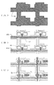
〔実施例1〕 図1に本実施例の作製工程断面図、図2に本実施例の作製工程平面図をそれぞれ示す。基板1としては透明なガラス基板、例えば、本実施例ではコーニング7059を用いる。基板1上にはスパッタ法によってタンタル膜を100〜3000Å、例えば、1000Å形成し、これを公知のフォトリソグラフィー法によって加工して、遮光膜2を得る。この段階で上方より見た様子を図2(A)に示す。同図に示すように、遮光膜2のパターンは画素を分離するパターンである。なお遮光膜2は図示しないコモン電極に延在し、そこには液晶パネル外から適当な電位が与えられる。(図2(A))
【0014】
次に、公知のプラズマCVD法によって厚さ500〜5000Å、例えば、2500Åの酸化珪素膜3を堆積する。酸化珪素膜3はTFTの下地絶縁膜として機能する。(図1(A))
次いで、公知のプラズマCVD法もしくは減圧CVD法により厚さ100〜1500Å、例えば、500Åの非晶質珪素膜を堆積し、公知の熱アニール法もしくはレーザーアニール法等の手段によってこれを結晶化させる。さらに、公知のフォトリソグラフィー法によって、結晶化した珪素膜を島状に分離し、活性層(島状領域)4を得る。
【0015】
次に、公知のプラズマCVD法により、厚さ500〜3000Åの酸化珪素膜5を堆積する。酸化珪素膜5はTFTのゲイト絶縁膜として機能する。さらに、厚さ2000〜8000Å、例えば、6000Åのアルミニウム(もしくはアルミニウム合金)膜をスパッタ法によって堆積し、これを公知のフォトリソグラフィー法によって加工し、ゲイト電極と配線(ゲイトバスライン)6を形成する。(図1(B))
【0016】
図2(B)にはこの段階で上方より見た様子を示す。同図に示されるようにゲイトバスライン6は平行に複数形成され、それらは先に形成されたタンタルの遮光膜のパターン2上に存在する。また、活性層4は、その一部15が先に形成された遮光膜のパターン2と重なるように形成される。(図2(B))
【0017】
次いで、公知の不純物拡散技術、例えば、イオンドーピング法によりゲイトバスライン6をマスクとして、活性層4にN型の不純物を導入する。ドーピング後は熱アニール法もしくはレーザーアニール法によって、再結晶化をおこなう。かくして、ソース7、ドレイン8が得られる。なお、以下の記述でドレインとは単に画素電極の接続される方の不純物領域のことを意味する。
次に公知のプラズマCVD法により厚さ3000〜8000Å、例えば、5000Åの窒化珪素膜9を堆積する。窒化珪素膜9は第1の層間絶縁物として機能する。窒化珪素の代わりに酸化珪素を用いてもよい。(図1(C))
【0018】
次いで、窒化珪素膜9にソース7およびドレイン8に通じるコンタクトホールを形成し、公知のスパッタ法によりアルミニウム合金膜もしくはアルミニウムとチタンの多層膜を堆積し、これを公知のフォトリソグラフィー法により加工し、ソースバスライン10、ドレイン電極11を形成する。図2(C)にはこの段階で上方より見た様子を示す。同図に示されるようにソースバスライン10は平行に複数形成され、また、個々の活性層4と各1つのコンタクトを有する。また、ソースバスライン10は先に形成されたタンタルの遮光膜のパターン2上に存在する。(図2(C))
【0019】
その後、公知のプラズマCVD法により厚さ3000〜8000Å、例えば、5000Åの酸化珪素膜12を堆積する。酸化珪素膜12は第2の層間絶縁物として機能する。酸化珪素の代わりに窒化珪素を用いてもよい。(図1(D))
次に、ポリイミド膜を塗布し、表面の平坦化をおこなう。この工程でポリイミド膜13が形成される。次いで、ポリイミド膜13をエッチングして、ドレイン電極11に通じるコンタクトホールを形成する。
【0020】
そして、公知のスパッタ法によって、透明導電性被膜、例えば、インディウム錫酸化物被膜を500〜2000、例えば、1000Å堆積し、これを公知のフォトリソグラフィー法を用いて加工し、画素電極14を得る。画素電極は遮光膜2と重なるようにパターンを形成する。かくすることにより漏光を防止することができる。(図1(E))
かくして、アクティブマトリクス回路が完成する。本実施例では、TFTがNチャネル型であり、かつ、TFTのチャネルの下に遮光膜2が形成されている。TFTに印加される電位がいかなる場合にも遮光膜2によってON状態とならないためには、遮光膜2にはTFTのソースもしくはドレインに印加される可能性のある最低電位よりも低い電位を付与することが望まれる。
【0021】
かくして、遮光膜2とドレイン8(活性層4)との間に容量が形成され、かつ、この容量は画素電極と並列に存在するので、画素容量の補助容量(保持容量)となる。もちろん、遮光膜2が存在するため、TFTのチャネルに光が入射することが防止され、TFTの特性が安定する。
【0022】
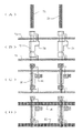
〔実施例2〕 図3を用いて本実施例を説明する。本実施例のTFT作製工程自体は実施例1と同じであるが、遮光膜、各バスライン、活性層等の配置が異なる。図3の番号は実施例1のものに対応する。
まず、実施例1と同様にタンタルで遮光膜のパターン2を形成する。これを図3(A)に示す。(図3(A))
【0023】
次いで、活性層4とゲイトバスライン6を形成する。ここで、ゲイトバスライン6と活性層4は共に遮光膜2の内側に配置される。(図3(B))
さらに、データバスライン10、ドレイン電極11を形成する。ここでも、データバスライン10、ドレイン電極11は遮光膜2の内側に配置される。(図3(C))
かくして、活性層、ゲイトバスライン、データバスライン、ドレイン電極のいずれもが遮光膜2の内側に形成され、これらは遮光膜2によって遮光される。
【0024】
〔実施例3〕 図4に本実施例の作製工程断面図、図5に本実施例の作製工程平面図をそれぞれ示す。基板41としてはコーニング1737を用いる。基板41上にはスパッタ法によってタンタル膜を2000Å形成し、これをフォトリソグラフィー法によって加工して、遮光膜42を得る。この段階で上方より見た様子を図5(A)に示す。同図に示すように、遮光膜42のパターンはゲイトバスライン(ゲイト電極を含む)とソースバスラインと重なり、画素を分離するパターンである。(図5(A))
【0025】
次に、プラズマCVD法によって厚さ1500Åの酸化珪素膜43を堆積する。酸化珪素膜43はTFTの下地絶縁膜として機能する。(図4(A))
次いで、減圧CVD法により厚さ800Åの非晶質珪素膜を堆積し、熱アニール法によってこれを結晶化させ、フォトリソグラフィー法によって、これを島状に分離し、活性層(島状領域)44を得る。さらに、プラズマCVD法により、厚さ1000Åの酸化珪素膜45を堆積する。酸化珪素膜45はTFTのゲイト絶縁膜として機能する。(図4(B))
【0026】
次に、イオンドーピング法により活性層44にN型の不純物を選択的に導入する。ドーピング後は熱アニール法またはレーザーアニール法によって、再結晶化をおこなう。かくして、ソース47、ドレイン48が得られる。さらに、厚さ5000Åのアルミニウム−チタン合金膜をスパッタ法によって堆積し、これをフォトリソグラフィー法によって加工し、ゲイトバスライン46a(当該画素のゲイト電極として機能する部分)およびゲイトバスライン46b(次行のゲイト電極として機能する部分)を形成する。ゲイトバスライン46bは当該画素の活性層44のドレイン48と重なるように形成される。
【0027】
図5(B)にはこの段階で上方より見た様子を示す。同図に示されるようにゲイトバスライン46aおよび46bは平行に複数形成され、それらは先に形成されたタンタルの遮光膜のパターン42上に存在する。また、活性層44は、その一部が先に形成された遮光膜のパターン42と重なるように、また、他の部分が次行のゲイトバスラインと重なるように形成される。(図5(B))
次にプラズマCVD法により厚さ5000Åの窒化珪素膜49を堆積する。窒化珪素膜49は第1の層間絶縁物として機能する。窒化珪素の代わりに酸化珪素を用いてもよい。(図4(C))
【0028】
次いで、窒化珪素膜49にソース47およびドレイン48に通じるコンタクトホールを形成し、スパッタ法によりアルミニウムとチタンの多層膜を堆積し、これをフォトリソグラフィー法により加工し、ソースバスライン50、ドレイン電極51を形成する。図5(C)にはこの段階で上方より見た様子を示す。同図に示されるようにソースバスライン50は平行に複数形成され、また、個々の活性層44と各1つのコンタクトを有する。また、ソースバスライン50は先に形成されたタンタルの遮光膜のパターン42上に存在する。(図5(C))
その後、プラズマCVD法により厚さ5000Åの酸化珪素膜52を堆積する。酸化珪素膜52は第2の層間絶縁物として機能する。酸化珪素の代わりに窒化珪素を用いてもよい。(図4(D))
【0029】
次に、ポリイミド膜の平坦化膜53を形成し、これをエッチングして、ドレイン電極51に通じるコンタクトホールを形成する。そして、スパッタ法によって、インディウム錫酸化物被膜を1500Å堆積し、これをフォトリソグラフィー法を用いて加工し、画素電極54を得る。画素電極は遮光膜2と重なるようにパターンを形成する。かくすることにより漏光を防止することができる。(図4(E))
かくして、アクティブマトリクス回路が完成する。本実施例も実施例1と同様にNチャネル型であり、遮光膜42にはTFTのソースもしくはドレインに印加される可能性のある最低電位よりも低い電位を付与することが望まれる。
【0030】
本実施例では、実施例1と同様に、遮光膜42とドレイン48(活性層44)との間に容量55(図4(E)の矢印)が形成される。しかしながら、そればかりではなく、ドレイン48と次行のゲイトバスラインとの間にも容量56(図4(E)の矢印)が形成される。容量55の一部と容量56は立体的に形成されるため、開口率を低下させることなく、実施例1の場合よりも、より多くの容量が補助容量として用いられる。
【0031】
本実施例では、容量56を形成するために、次行のゲイトバスラインを用いたが、回路配置上、開口率が低下するという問題はあるが、ゲイトバスラインと同じ層内の電位の固定された配線を用いてもよい。ゲイトバスラインを容量の一方の電極として用いる場合には、容量がゲイト信号の影響を受け、したがって、マトリクスの走査方向が固定されるのに対し、ゲイト信号と独立した電位に保持された配線を用いると、走査方向は上からでも下からでも任意に設定できる。
【0032】
〔実施例4〕 図6を用いて本実施例を説明する。本実施例のTFT作製工程自体は実施例2と同じであるが、遮光膜、各バスライン、活性層等の配置が異なる。図6の番号は実施例2のものに対応する。
まず、実施例2と同様にタンタルで遮光膜のパターン42を形成する。これを図6(A)に示す。(図6(A))
【0033】
次いで、活性層44とゲイトバスライン46を形成する。ここで、ゲイトバスライン46と活性層44は共に遮光膜42の内側に配置される。(図6(B))
さらに、データバスライン50、ドレイン電極51を形成する。ここでも、データバスライン50、ドレイン電極51は遮光膜42の内側に配置される。(図6(C))
かくして、活性層、ゲイトバスライン、データバスライン、ドレイン電極のいずれもが遮光膜42の内側に形成され、これらは遮光膜42によって遮光される。
【0034】
〔実施例5〕 図7に本実施例の作製工程断面図、図8に本実施例の作製工程平面図をそれぞれ示す。基板71としてはコーニング1737を用いる。基板71上にはスパッタ法によってタンタル膜を1000Å形成し、これをフォトリソグラフィー法によって加工して、遮光膜72を得る。この段階で上方より見た様子を図8(A)に示す。同図に示すように、遮光膜72のパターンはソースバスラインと重なるパターンである。(図8(A))
【0035】
次に、プラズマCVD法によって厚さ2000Åの酸化珪素膜73を堆積する。酸化珪素膜73はTFTの下地絶縁膜として機能する。(図7(A))
次いで、減圧CVD法により厚さ1000Åの非晶質珪素膜を堆積し、レーザーアニール法によってこれを結晶化させ、フォトリソグラフィー法によって、これを島状に分離し、活性層(島状領域)74を得る。さらに、プラズマCVD法により、厚さ1200Åの酸化珪素膜75を堆積する。酸化珪素膜75はTFTのゲイト絶縁膜として機能する。
【0036】
次に、厚さ5000Åのアルミニウム−チタン合金膜をスパッタ法によって堆積し、これをフォトリソグラフィー法によって加工し、ゲイトバスライン76を形成する。(図7(B))
図8(B)にはこの段階で上方より見た様子を示す。同図に示されるようにゲイトバスライン76は平行に複数形成され、それらは先に形成されたタンタルの遮光膜のパターン72と直交する。また、活性層74は、その一部が先に形成された遮光膜のパターン72と重なるように形成される。(図8(B))
【0037】
さらに、イオンドーピング法により活性層74にゲイトバスライン76をマスクとしてN型の不純物を導入する。ドーピング後はレーザーアニール法によって、再結晶化をおこなう。かくして、ソース77、ドレイン78が得られる。
次にプラズマCVD法により厚さ5000Åの窒化珪素膜79を堆積する。窒化珪素膜79は第1の層間絶縁物として機能する。窒化珪素の代わりに酸化珪素を用いてもよい。(図7(C))
【0038】
次いで、窒化珪素膜79にソース77およびドレイン78に通じるコンタクトホールを形成し、スパッタ法によりアルミニウムとチタンの多層膜を堆積し、これをフォトリソグラフィー法により加工し、ソースバスライン80、ドレイン電極81を形成する。図8(C)にはこの段階で上方より見た様子を示す。同図に示されるようにソースバスライン80は平行に複数形成され、また、個々の活性層74と各1つのコンタクトを有する。また、ソースバスライン80は先に形成されたタンタルの遮光膜のパターン72上に存在する。(図8(C))
【0039】
その後、プラズマCVD法により厚さ5000Åの酸化珪素膜82を堆積する。酸化珪素膜82は第2の層間絶縁物として機能する。酸化珪素の代わりに窒化珪素を用いてもよい。(図7(D))
次に、スパッタ法によって厚さ1000Åのクロム膜を堆積し、これをパターン形成して上層の遮光膜85を形成する。この段階で上方より見た様子を図8(D)に示す。同図より明らかなように上層の遮光膜はゲイトバスラインを隠すように形成される。
【0040】
さらに、ポリイミド膜の平坦化膜83を形成し、これをエッチングして、ドレイン電極81に通じるコンタクトホールを形成する。遮光膜85とポリイミド膜83の間には何らかの無機材料被膜を設けて、密着性を強化してもよい。そして、スパッタ法によって、インディウム錫酸化物被膜を1500Å堆積し、これをフォトリソグラフィー法を用いて加工し、画素電極84を得る。画素電極84と上層の遮光膜85は一部重なるように配置する。(図7(E))
かくして、アクティブマトリクス回路が完成する。本実施例も実施例1および3と同様にNチャネル型であるが、遮光膜72はTFTの活性層のうち、チャネルと重なっていないので、遮光膜72の電位がいかなるものであれ、TFTに与える影響はない。この点で他の実施例のものよりも優れている。
【0041】
本実施例では、実施例1と同様に、遮光膜72とドレイン78(活性層74)との間に容量が形成される。そればかりではなく、上層の遮光膜85にも適切な電位を付与することにより、画素電極84との間にも容量が形成される。画素電極84は当該画素を駆動するゲイトバスライン76により影響を受けることは避けなければならないが、本実施例では、ゲイトバスラインを覆って導電性の遮光膜85が設けられるので、画素電極84とゲイトバスライン76とのカップリングは十分に低減される。
【0042】
さらに、本実施例では、下層の遮光膜72はソースバスライン80と、上層の遮光膜85はゲイトバスライン76と、それぞれ重なって配置されるが、各遮光膜とバスラインの間には十分な絶縁層があるので、バスラインに対する寄生容量は極限にまで低減できる。
なお、本実施例ではTFTのチャネル部分は上層の遮光膜85によってのみ遮光される構造となっているが、下層の遮光膜72によっても遮光されるようなパターンとするとTFTの動作を安定させる上でより効果的である。
【0043】
〔実施例6〕 図9を用いて本実施例を説明する。本実施例のTFT作製工程自体は実施例3と同じであるが、遮光膜、各バスライン、活性層等の配置が異なる。図9の番号は実施例3のものに対応する。
まず、実施例3と同様にタンタルで遮光膜のパターン72を形成する。これを図9(A)に示す。(図9(A))
【0044】
次いで、活性層74とゲイトバスライン76を形成する。ここで、ゲイトバスライン76と活性層74は共に遮光膜72の内側に配置される。(図9(B))
さらに、データバスライン80、ドレイン電極81を形成する。ここでもドレイン電極81は遮光膜72の内側に配置される。かくして、活性層、ゲイトバスライン、ドレイン電極のいずれもが遮光膜72の内側に形成され、これらは遮光膜72によって遮光される。(図9(C))
【0045】
次に、上層の遮光膜85を形成する。本実施例では場合は、遮光膜85は分離して与えられるので、導電性である必要はなく、絶縁性のものでもよい。また、遮光膜85はデータバスライン80を隠すように形成する。かくして、データバスライン80は遮光膜72と上層の遮光膜85によって覆われる。(図9(D))
本実施例は実施例1〜4と同様に遮光膜72がTFTのチャネルと重なるので、その電位はTFTのソース、ドレインに印加される電位よりも低い(Nチャネル型の場合)もしくは高い(Pチャネル型の場合)ことが望ましい。
【0046】
〔実施例7〕 図10に本実施例の作製工程断面図を示す。本実施例は、遮光膜として形成されるタンタル膜の一部を外部とのボンディング端子に用いる例である。基板91としてはコーニング1737を用いる。基板91上にはスパッタ法によってタンタル膜を1000Å形成し、これをフォトリソグラフィー法によって加工して、遮光膜92bおよびボンディング端子電極92aを得る。ボンディング端子電極92aおよび遮光膜92bはこの段階では電気的に接続されている。そして、プラズマCVD法によって厚さ2000Åの酸化珪素膜93を堆積する。酸化珪素膜93はTFTの下地絶縁膜として機能する。(図10(A))
【0047】
次いで、結晶性珪素膜によって活性層(島状領域)94を得る。さらに、プラズマCVD法により、厚さ1200Åの酸化珪素膜95を堆積する。酸化珪素膜95はTFTのゲイト絶縁膜として機能する。
次に、酸化珪素膜94および95をエッチングして、ボンディング端子電極92aにコンタクトホール96aおよび96bを形成する。前者はボンディング箇所であり、後者はゲイトバスラインとのコンタクトを得る場所である。(図10(B))
【0048】
そして、厚さ5000Åのアルミニウム−チタン合金膜によって、ゲイトバスライン97aおよび97bを形成する。この段階では、ゲイトバスライン97aおよび97bは電気的に接続している。そして、ゲイトバスライン97aがボンディング端子電極92aと接触しているため、ボンディング端子電極92a、遮光膜92b、およびゲイトバスライン97aおよび97bは全て同電位に保たれている。かくすると帯電現象によるゲイト絶縁膜の破壊は極力抑えられる。(図10(C))
【0049】
さらに、イオンドーピング法により活性層94にゲイトバスライン97bをマスクとしてN型の不純物を導入し、ソース98、ドレイン99を得る。そして、プラズマCVD法により厚さ5000Åの窒化珪素膜100(第1の層間絶縁物)を堆積する。
次いで、窒化珪素膜100にソース98およびドレイン99に通じるコンタクトホールを形成し、スパッタ法によりアルミニウムとチタンの多層膜を堆積し、これをフォトリソグラフィー法により加工し、ソースバスライン101、ドレイン電極102を形成する。そして、この段階でボンディング端子電極92aと遮光膜92b、およびゲイトバスライン97aと97bを機械的に切断する。(図10(D))
【0050】
その後、プラズマCVD法により厚さ3000Åの窒化珪素膜103(第2の層間絶縁物)を堆積する。(図10(E))
さらに、ポリイミド膜の平坦化膜104を形成し、これと2つの窒化珪素膜100および103をエッチングして、ドレイン電極102およびボンディング端子電極92aに通じるコンタクトホールを形成する。このエッチング工程においてはドレイン電極102がエッチングストッパーとして機能せしめてもよい。
そして、スパッタ法によって、インディウム錫酸化物(ITO)被膜を1500Å堆積し、これをフォトリソグラフィー法を用いて加工し、ボンディング端子105aおよび画素電極105bを得る。(図10(F))
【0051】
このようにして作製したアクティブマトリクス回路のTFTとボンディング部分が完成する。ボンディングは、ボンディング端子105aにおいて形成されるが、ボンディング端子92aの、特にコンタクトホール96aにおいておこなうとよい。該部分はタンタル膜とITO膜との多層領域であり、機械的に強固であるため、ボンディングの目的に適している。例えば、層間絶縁物上のITO膜では、下層の層間絶縁物がさまざまな応力にさらされているため、例えば、膜の剥離が生じたりして、十分な接続が得られない。しかしながら、コンタクトホール96aの部分では下地は基板そのものであり、機械的に非常に安定している。
【0052】
【発明の効果】
本発明によって、遮光膜を補助容量として有効に利用できる。実施例では結晶性珪素を用いたTFTを取り上げたが、非晶質珪素を用いたTFT、その他の半導体を用いたTFTであっても同様に実施できることは自明である。また、(下層の)遮光膜もタンタル以外のものでも、導電性で、かつ、その後のプロセスに耐えるものであれば何ら問題なく使用できる。このように本発明は工業上有用である。
【図面の簡単な説明】
【図1】本発明の実施例を説明する工程断面図である。(実施例1)
【図2】本発明の実施例を説明する工程平面図である。(実施例1)
【図3】本発明の実施例を説明する工程平面図である。(実施例2)
【図4】本発明の実施例を説明する工程断面図である。(実施例3)
【図5】本発明の実施例を説明する工程平面図である。(実施例3)
【図6】本発明の実施例を説明する工程平面図である。(実施例4)
【図7】本発明の実施例を説明する工程断面図である。(実施例5)
【図8】本発明の実施例を説明する工程平面図である。(実施例5)
【図9】本発明の実施例を説明する工程平面図である。(実施例6)
【図10】本発明の実施例を説明する工程平面図である。(実施例7)
【符号の説明】
1、41、71、91 基板
2、42、72、92 (下層の)遮光膜
3、43、73、93 下地絶縁膜
4、44、74、94 半導体層
5、45、75、95 ゲイト絶縁膜
6、46、76、97 ゲイト電極(ゲイトバスライン)
7、47、77、98 ソース
8、48、78、99 ドレイン
9、49、79、100 第1層間絶縁物
10、50、80、101 ソースバスライン
11、51、81、102 金属電極
12、52、82、103 第2層間絶縁物
13、53、83、104 平坦化膜
14、54、84、105 画素電極(透明導電膜)
15、55、56 容量
85 上層の遮光膜
96 下層の遮光膜に対するコンタクトホール[0001]
BACKGROUND OF THE INVENTION
The present invention generally relates to a liquid crystal display device, and more particularly to a liquid crystal display device having a feature in the arrangement of a light-shielding film on a substrate carrying a TFT (thin film transistor) among a pair of opposing substrates constituting a liquid crystal panel.
[0002]
[Prior art]
Liquid crystal display devices are widely used as projection type or direct view type display devices. In particular, in order to achieve high-resolution color display, a so-called active matrix liquid crystal display device in which each pixel is driven by a thin film transistor (TFT) is suitable. By using the active matrix driving method, crosstalk between pixels that occurs in the simple matrix method can be eliminated, and excellent display characteristics can be obtained.
[0003]
In such an active matrix driving method, TFTs are arranged on one side of a glass substrate constituting a liquid crystal panel, and each TFT controls a voltage applied to a corresponding transparent pixel electrode. A TFT is a semiconductor element, and its characteristics fluctuate when exposed to light directly from the outside. Therefore, a structure that prevents external light is required. In particular, in a projection display device, since strong light is irradiated, light shielding is an important issue.
[0004]
On the other hand, light is leaked at the boundary portion of each pixel of the liquid crystal display device due to the influence of the electric field of the adjacent pixel. In order to improve the contrast ratio of display, it is necessary to minimize the light leaking through such a TFT forming portion, and therefore a structure in which such a boundary portion is not used for display has been proposed. Such a structure is called a black matrix (also abbreviated as BM). Since the black matrix itself has a light blocking effect, it is also used for the above-described light blocking purpose. A black matrix or a structure having a simple light-shielding effect is also called a light-shielding film because it is in the form of a film.
[0005]
Conventionally, a light-shielding film (black matrix) is formed on a substrate facing the substrate carrying the TFT. However, in such a configuration, precise alignment between the substrates is necessary so that the light shielding film covers the corresponding TFT, and therefore, the assembly process of the liquid crystal panel takes time. If the light-shielding pattern is formed larger in order to facilitate the alignment operation, problems such as a decrease in display brightness occur.
[0006]
In order to solve the above problem, the light shielding film may be formed on the same substrate carrying the TFT. The light shielding film was formed in a layer above or below the semiconductor layer. That is, in the case of the former, in the TFT manufacturing process, the light shielding film is formed in the final stage, and in the case of the latter, it is formed in the initial stage.
[0007]
[Problems to be solved by the invention]
Conventional light-shielding films have been used only for light-shielding purposes. However, it is wasteful in terms of mass productivity to add a film forming process or an etching / patterning process only for that purpose. In view of this, the present inventor has an object to provide a structure in which a light shielding film is made conductive and can be used also for a storage capacitor of a pixel.
[0008]
[Means for Solving the Problems]
The present invention uses an active matrix circuit having a structure in which a top gate type structure (a structure in which a semiconductor layer (active layer) is provided on a substrate and a gate electrode is provided thereon) as a TFT and a light shielding film is provided below the semiconductor layer. Is featured. The light shielding film has a structure in which at least one of the source bus line and the gate bus line is hidden (overlapped).
[0009]
The main light is incident from the substrate side.
In addition, the light shielding film overlaps a region (drain) electrically connected to the pixel electrode in the semiconductor layer via an insulating layer, and the capacitance between the light shielding film and the drain is maintained by maintaining the light shielding film at an appropriate potential. Form. Since this capacity is in parallel with the capacity of the pixel electrode (pixel capacity), it can be used as an auxiliary capacity (retention capacity).
[0010]
Of course, in addition to the capacitance between the light shielding film and the semiconductor layer as described above, the capacitance between the semiconductor layer and the gate bus line or other wiring in another row may be combined. The thickness of the insulating film existing between the semiconductor layer and the light shielding film is preferably at least twice the thickness of the gate insulating film of the TFT. The light shielding film is desirably thicker than the source bus line and the gate bus line, and has a structure capable of shielding these. The light shielding film is fixed at an appropriate potential. For example, the light shielding film is connected to an external terminal of the liquid crystal panel, and an appropriate potential is applied from the outside.
[0011]
Further, when a mechanically strong material such as tantalum or titanium is used, such a light shielding film can also be used as an external contact terminal.
Since the auxiliary capacitance is formed so as to overlap the light shielding film, the aperture ratio is not lowered in terms of circuit design.
In the present invention, the light shielding film may have a shape that hides the entire semiconductor layer or a shape that partially overlaps.
[0012]
In addition to the light shielding film provided below the semiconductor layer as described above, a light shielding film (referred to as an upper light shielding film) may also be provided above the element. In particular, when an upper light shielding film is provided in the TFT portion, stray light incident on the TFT can be reduced to the limit, which is effective in stabilizing the operation of the TFT.
In this case, the upper light shielding film may be conductive or insulating. When the upper light shielding film is conductive, a capacitor may be formed between the upper light shielding film and the pixel electrode. In this case, if the upper light-shielding layer and the lower light-shielding layer are arranged so as to overlap with each other, two capacitors having different layers can be formed at the same position, which is effective in integration of elements.
[0013]
【Example】
Example 1 FIG. 1 is a cross-sectional view of a manufacturing process of this example, and FIG. 2 is a plan view of the manufacturing process of this example. As the substrate 1, a transparent glass substrate, for example, Corning 7059 in this embodiment is used. A tantalum film having a thickness of 100 to 3000 mm, for example, 1000 mm, is formed on the substrate 1 by sputtering, and this is processed by a known photolithography method to obtain the light-
[0014]
Next, a
Next, an amorphous silicon film having a thickness of 100 to 1500 mm, for example, 500 mm is deposited by a known plasma CVD method or low pressure CVD method, and crystallized by means such as a known thermal annealing method or laser annealing method. Further, the crystallized silicon film is separated into islands by a known photolithography method, and an active layer (island region) 4 is obtained.
[0015]
Next, a silicon oxide film 5 having a thickness of 500 to 3000 mm is deposited by a known plasma CVD method. The silicon oxide film 5 functions as a gate insulating film of the TFT. Further, an aluminum (or aluminum alloy) film having a thickness of 2000 to 8000 mm, for example, 6000 mm is deposited by a sputtering method, and this is processed by a known photolithography method to form a gate electrode and a wiring (gate bus line) 6. . (Fig. 1 (B))
[0016]
FIG. 2B shows a state seen from above at this stage. As shown in the figure, a plurality of
[0017]
Next, an N-type impurity is introduced into the active layer 4 using the
Next, a
[0018]
Next, contact holes leading to the
[0019]
Thereafter, a
Next, a polyimide film is applied to flatten the surface. In this step, the
[0020]
Then, a transparent conductive film, for example, an indium tin oxide film, is deposited in a thickness of 500 to 2000, for example, 1000 mm by a known sputtering method, and this is processed using a known photolithography method to obtain the
Thus, the active matrix circuit is completed. In this embodiment, the TFT is an N-channel type, and the
[0021]
Thus, a capacitance is formed between the light-shielding
[0022]
Example 2 This example will be described with reference to FIG. The TFT manufacturing process itself of this example is the same as that of Example 1, but the arrangement of the light shielding film, each bus line, the active layer, and the like is different. The numbers in FIG. 3 correspond to those in the first embodiment.
First, the light
[0023]
Next, the active layer 4 and the
Further, the
Thus, all of the active layer, the gate bus line, the data bus line, and the drain electrode are formed inside the
[0024]
[Embodiment 3] FIG. 4 is a cross-sectional view of a manufacturing process of this embodiment, and FIG. 5 is a plan view of the manufacturing process of this embodiment. Corning 1737 is used as the substrate 41. A 2000 mm tantalum film is formed on the substrate 41 by sputtering, and this is processed by photolithography to obtain the light-shielding
[0025]
Next, a
Next, an amorphous silicon film having a thickness of 800 mm is deposited by a low pressure CVD method, crystallized by a thermal annealing method, separated into island shapes by a photolithography method, and an active layer (island region) 44 is obtained. Get. Further, a
[0026]
Next, an N-type impurity is selectively introduced into the
[0027]
FIG. 5B shows a state seen from above at this stage. As shown in the figure, a plurality of
Next, a
[0028]
Next, contact holes that lead to the
Thereafter, a
[0029]
Next, a
Thus, the active matrix circuit is completed. This embodiment is also an N-channel type like the first embodiment, and it is desirable to apply a potential lower than the lowest potential that can be applied to the source or drain of the TFT to the
[0030]
In the present embodiment, as in the first embodiment, a capacitor 55 (an arrow in FIG. 4E) is formed between the
[0031]
In this embodiment, the gate bus line of the next row is used to form the
[0032]
[Embodiment 4] This embodiment will be described with reference to FIG. The TFT manufacturing process itself of this example is the same as that of Example 2, but the arrangement of the light shielding film, each bus line, the active layer, and the like is different. The numbers in FIG. 6 correspond to those in the second embodiment.
First, a light
[0033]
Next, the
Further, the
Thus, all of the active layer, the gate bus line, the data bus line, and the drain electrode are formed inside the
[0034]
[Embodiment 5] FIG. 7 is a sectional view of a manufacturing process of this embodiment, and FIG. 8 is a plan view of the manufacturing process of this embodiment. Corning 1737 is used as the
[0035]
Next, a
Next, an amorphous silicon film having a thickness of 1000 mm is deposited by a low pressure CVD method, crystallized by a laser annealing method, separated into island shapes by a photolithography method, and an active layer (island region) 74 is obtained. Get. Further, a
[0036]
Next, an aluminum-titanium alloy film having a thickness of 5000 mm is deposited by a sputtering method and processed by a photolithography method to form the
FIG. 8B shows a state seen from above at this stage. As shown in the figure, a plurality of
[0037]
Further, an N-type impurity is introduced into the
Next, a
[0038]
Next, contact holes that lead to the
[0039]
Thereafter, a
Next, a chromium film having a thickness of 1000 mm is deposited by sputtering, and this is patterned to form an upper
[0040]
Further, a
Thus, the active matrix circuit is completed. This embodiment is also an N channel type as in the first and third embodiments. However, since the
[0041]
In the present embodiment, a capacitor is formed between the
[0042]
Further, in this embodiment, the lower light-shielding
In this embodiment, the channel portion of the TFT is structured so as to be shielded only by the upper
[0043]
Example 6 This example will be described with reference to FIG. The TFT manufacturing process itself of this example is the same as that of Example 3, but the arrangement of the light shielding film, each bus line, the active layer, and the like is different. The numbers in FIG. 9 correspond to those in the third embodiment.
First, a light-shielding
[0044]
Next, an
Further, the
[0045]
Next, an upper
In this embodiment, since the
[0046]
[Embodiment 7] FIG. 10 shows a sectional view of a manufacturing process of this embodiment. In this embodiment, a part of a tantalum film formed as a light shielding film is used as a bonding terminal with the outside. Corning 1737 is used as the
[0047]
Next, an active layer (island region) 94 is obtained from the crystalline silicon film. Further, a
Next, the
[0048]
Then, the
[0049]
Further, an N-type impurity is introduced into the
Next, contact holes that lead to the
[0050]
Thereafter, a silicon nitride film 103 (second interlayer insulator) having a thickness of 3000 mm is deposited by plasma CVD. (Fig. 10 (E))
Further, a
Then, 1500 μm of indium tin oxide (ITO) film is deposited by sputtering, and this is processed using a photolithography method to obtain
[0051]
The TFT and bonding portion of the active matrix circuit thus fabricated are completed. The bonding is formed at the
[0052]
【The invention's effect】
According to the present invention, the light shielding film can be effectively used as an auxiliary capacitor. In the examples, TFTs using crystalline silicon are taken up. However, it is obvious that TFTs using amorphous silicon and TFTs using other semiconductors can be similarly implemented. In addition, the light shielding film (lower layer) other than tantalum can be used without any problem as long as it is conductive and can withstand subsequent processes. Thus, the present invention is industrially useful.
[Brief description of the drawings]
FIG. 1 is a process cross-sectional view illustrating an embodiment of the present invention. (Example 1)
FIG. 2 is a process plan view illustrating an embodiment of the present invention. (Example 1)
FIG. 3 is a process plan view illustrating an embodiment of the present invention. (Example 2)
FIG. 4 is a process cross-sectional view illustrating an embodiment of the present invention. (Example 3)
FIG. 5 is a process plan view illustrating an embodiment of the present invention. (Example 3)
FIG. 6 is a process plan view illustrating an embodiment of the present invention. (Example 4)
FIG. 7 is a process cross-sectional view illustrating an embodiment of the present invention. (Example 5)
FIG. 8 is a process plan view illustrating an embodiment of the present invention. (Example 5)
FIG. 9 is a process plan view illustrating an embodiment of the present invention. (Example 6)
FIG. 10 is a process plan view illustrating an embodiment of the present invention. (Example 7)
[Explanation of symbols]
1, 41, 71, 91 substrate
2, 42, 72, 92 (underlayer) light shielding film
3, 43, 73, 93 Underlying insulating film
4, 44, 74, 94 Semiconductor layer
5, 45, 75, 95 Gate insulation film
6, 46, 76, 97 Gate electrode (Gate bus line)
7, 47, 77, 98 source
8, 48, 78, 99 Drain
9, 49, 79, 100 First interlayer insulator
10, 50, 80, 101 Source bus line
11, 51, 81, 102 Metal electrode
12, 52, 82, 103 Second interlayer insulator
13, 53, 83, 104 Planarization film
14, 54, 84, 105 Pixel electrode (transparent conductive film)
15, 55, 56 capacity
85 Upper light shielding film
96 Contact hole for the underlying light shielding film
Claims (4)
前記アクティブマトリクス回路において、
前記TFTの半導体層は、チャネル、前記ソースバスラインと電気的に接続される第 1 の領域、および画素電極に電気的に接続される第2の領域を有し、
一定の電位に固定された遮光膜を前記半導体層の下に有し、
ソースバスラインもしくはゲイトバスラインのうち少なくともソースバスラインは、前記遮光膜上に形成され、
前記第2の領域の一部は前記ソースバスラインに覆われ、かつ前記ソースバスラインの下方において、前記遮光膜と絶縁層を介して重なって、補助容量を形成することを特徴とする液晶表示装置。A liquid crystal display device having an active matrix circuit using a top gate type TFT as a switching element,
In the active matrix circuit,
The semiconductor layer of the TFT has a channel, a first region electrically connected to the source bus line, and a second region electrically connected to the pixel electrode,
A light-shielding film fixed at a constant potential below the semiconductor layer;
At least the source bus line of the source bus line or the gate bus line is formed on the light shielding film ,
A part of the second region is covered with the source bus line, and an auxiliary capacitor is formed below the source bus line by overlapping with the light shielding film via an insulating layer. apparatus.
Priority Applications (2)
| Application Number | Priority Date | Filing Date | Title |
|---|---|---|---|
| JP20537896A JP3708637B2 (en) | 1996-07-15 | 1996-07-15 | Liquid crystal display device |
| US08/891,697 US5966193A (en) | 1996-07-15 | 1997-07-11 | LCD device having coupling capacitances and shielding films |
Applications Claiming Priority (1)
| Application Number | Priority Date | Filing Date | Title |
|---|---|---|---|
| JP20537896A JP3708637B2 (en) | 1996-07-15 | 1996-07-15 | Liquid crystal display device |
Publications (2)
| Publication Number | Publication Date |
|---|---|
| JPH1031235A JPH1031235A (en) | 1998-02-03 |
| JP3708637B2 true JP3708637B2 (en) | 2005-10-19 |
Family
ID=16505843
Family Applications (1)
| Application Number | Title | Priority Date | Filing Date |
|---|---|---|---|
| JP20537896A Expired - Lifetime JP3708637B2 (en) | 1996-07-15 | 1996-07-15 | Liquid crystal display device |
Country Status (2)
| Country | Link |
|---|---|
| US (1) | US5966193A (en) |
| JP (1) | JP3708637B2 (en) |
Cited By (1)
| Publication number | Priority date | Publication date | Assignee | Title |
|---|---|---|---|---|
| CN103176323A (en) * | 2007-08-09 | 2013-06-26 | 精工爱普生株式会社 | Electro-optical device and electronic apparatus |
Families Citing this family (79)
| Publication number | Priority date | Publication date | Assignee | Title |
|---|---|---|---|---|
| TW479151B (en) * | 1996-10-16 | 2002-03-11 | Seiko Epson Corp | Substrate for liquid crystal device, the liquid crystal device and projection-type display |
| US6088070A (en) | 1997-01-17 | 2000-07-11 | Semiconductor Energy Laboratory Co., Ltd. | Active matrix liquid crystal with capacitor between light blocking film and pixel connecting electrode |
| JPH10221704A (en) * | 1997-02-07 | 1998-08-21 | Sharp Corp | Reflection type liquid crystal display device and its manufacture |
| JP3716580B2 (en) | 1997-02-27 | 2005-11-16 | セイコーエプソン株式会社 | Liquid crystal device and manufacturing method thereof, and projection display device |
| JP3784491B2 (en) * | 1997-03-28 | 2006-06-14 | 株式会社半導体エネルギー研究所 | Active matrix display device |
| KR100514672B1 (en) * | 1997-07-23 | 2005-09-13 | 세이코 엡슨 가부시키가이샤 | Liquid crystal display, method of manufacturing the liquid crystal display, and electronic equipment |
| JP4271268B2 (en) | 1997-09-20 | 2009-06-03 | 株式会社半導体エネルギー研究所 | Image sensor and image sensor integrated active matrix display device |
| JP3973787B2 (en) * | 1997-12-31 | 2007-09-12 | 三星電子株式会社 | Liquid crystal display device and manufacturing method thereof |
| JP3980156B2 (en) | 1998-02-26 | 2007-09-26 | 株式会社半導体エネルギー研究所 | Active matrix display device |
| US6556265B1 (en) * | 1998-03-19 | 2003-04-29 | Seiko Epson Corporation | LCD having auxiliary capacitance lines and light shielding films electrically connected via contact holes |
| JPH11274509A (en) | 1998-03-26 | 1999-10-08 | Sanyo Electric Co Ltd | Thin film transistor and liquid crystal display |
| JPH11326954A (en) * | 1998-05-15 | 1999-11-26 | Semiconductor Energy Lab Co Ltd | Semiconductor device |
| JP3433101B2 (en) | 1998-06-03 | 2003-08-04 | 三洋電機株式会社 | Display device |
| JP3702096B2 (en) * | 1998-06-08 | 2005-10-05 | 三洋電機株式会社 | Thin film transistor and display device |
| JP2000075280A (en) * | 1998-08-28 | 2000-03-14 | Sony Corp | Liquid crystal display device |
| JP3141860B2 (en) * | 1998-10-28 | 2001-03-07 | ソニー株式会社 | Manufacturing method of liquid crystal display device |
| US6617644B1 (en) * | 1998-11-09 | 2003-09-09 | Semiconductor Energy Laboratory Co., Ltd. | Semiconductor device and method of manufacturing the same |
| JP3458382B2 (en) * | 1998-11-26 | 2003-10-20 | セイコーエプソン株式会社 | ELECTRO-OPTICAL DEVICE, MANUFACTURING METHOD THEREOF, AND ELECTRONIC DEVICE |
| JP4758868B2 (en) * | 1998-11-26 | 2011-08-31 | セイコーエプソン株式会社 | Electro-optical device and electronic apparatus |
| WO2000033285A1 (en) * | 1998-11-30 | 2000-06-08 | Seiko Epson Corporation | Electro-optical device and its manufacturing method |
| US6850292B1 (en) * | 1998-12-28 | 2005-02-01 | Seiko Epson Corporation | Electric-optic device, method of fabricating the same, and electronic apparatus |
| US6590229B1 (en) * | 1999-01-21 | 2003-07-08 | Semiconductor Energy Laboratory Co., Ltd. | Semiconductor device and process for production thereof |
| EP1031873A3 (en) | 1999-02-23 | 2005-02-23 | Sel Semiconductor Energy Laboratory Co., Ltd. | Semiconductor device and fabrication method thereof |
| US6531993B1 (en) | 1999-03-05 | 2003-03-11 | Semiconductor Energy Laboratory Co., Ltd. | Active matrix type display device |
| JP2000258798A (en) * | 1999-03-05 | 2000-09-22 | Sanyo Electric Co Ltd | Display device |
| US6690434B1 (en) | 1999-03-15 | 2004-02-10 | Semiconductor Energy Laboratory Co., Ltd. | Active matrix liquid crystal display device |
| US6475836B1 (en) | 1999-03-29 | 2002-11-05 | Semiconductor Energy Laboratory Co., Ltd. | Semiconductor device and manufacturing method thereof |
| US6861670B1 (en) * | 1999-04-01 | 2005-03-01 | Semiconductor Energy Laboratory Co., Ltd. | Semiconductor device having multi-layer wiring |
| US6583471B1 (en) * | 1999-06-02 | 2003-06-24 | Semiconductor Energy Laboratory Co., Ltd. | Semiconductor device having first and second insulating films |
| US6777254B1 (en) | 1999-07-06 | 2004-08-17 | Semiconductor Energy Laboratory Co., Ltd. | Semiconductor device and fabrication method thereof |
| TW526355B (en) | 1999-07-14 | 2003-04-01 | Sanyo Electric Co | Reflection type liquid crystal display device |
| JP4403329B2 (en) * | 1999-08-30 | 2010-01-27 | ソニー株式会社 | Manufacturing method of liquid crystal display device |
| TW478014B (en) * | 1999-08-31 | 2002-03-01 | Semiconductor Energy Lab | Semiconductor device and method of manufacturing thereof |
| JP3374911B2 (en) * | 1999-09-30 | 2003-02-10 | 日本電気株式会社 | Transmissive liquid crystal panel, image display device, panel manufacturing method |
| CN1195243C (en) * | 1999-09-30 | 2005-03-30 | 三星电子株式会社 | Film transistor array panel for liquid crystal display and its producing method |
| US6587086B1 (en) * | 1999-10-26 | 2003-07-01 | Semiconductor Energy Laboratory Co., Ltd. | Electro-optical device |
| US6646287B1 (en) * | 1999-11-19 | 2003-11-11 | Semiconductor Energy Laboratory Co., Ltd. | Semiconductor device with tapered gate and insulating film |
| US6750835B2 (en) * | 1999-12-27 | 2004-06-15 | Semiconductor Energy Laboratory Co., Ltd. | Image display device and driving method thereof |
| JP3838332B2 (en) * | 2000-01-24 | 2006-10-25 | 日本電気株式会社 | Transmission type liquid crystal display device and liquid crystal projector device |
| TW495854B (en) * | 2000-03-06 | 2002-07-21 | Semiconductor Energy Lab | Semiconductor device and manufacturing method thereof |
| TW513753B (en) * | 2000-03-27 | 2002-12-11 | Semiconductor Energy Lab | Semiconductor display device and manufacturing method thereof |
| WO2001082273A1 (en) | 2000-04-21 | 2001-11-01 | Seiko Epson Corporation | Electrooptical device |
| US8610645B2 (en) * | 2000-05-12 | 2013-12-17 | Semiconductor Energy Laboratory Co., Ltd. | Display device |
| KR100623989B1 (en) * | 2000-05-23 | 2006-09-13 | 삼성전자주식회사 | Thin film transistor panels for liquid crystal display and methods for repairing the same |
| US6602765B2 (en) * | 2000-06-12 | 2003-08-05 | Seiko Epson Corporation | Fabrication method of thin-film semiconductor device |
| TW504846B (en) | 2000-06-28 | 2002-10-01 | Semiconductor Energy Lab | Semiconductor device and manufacturing method thereof |
| JP4684170B2 (en) * | 2000-06-28 | 2011-05-18 | 株式会社半導体エネルギー研究所 | Method for manufacturing semiconductor device |
| US6542205B2 (en) * | 2000-08-04 | 2003-04-01 | Semiconductor Energy Laboratory Co., Ltd. | Display device |
| JP4896314B2 (en) * | 2000-08-04 | 2012-03-14 | 株式会社半導体エネルギー研究所 | Display device |
| US6636284B2 (en) * | 2000-08-11 | 2003-10-21 | Seiko Epson Corporation | System and method for providing an electro-optical device having light shield layers |
| US6720577B2 (en) * | 2000-09-06 | 2004-04-13 | Semiconductor Energy Laboratory Co., Ltd. | Semiconductor device and method of manufacturing the same |
| JP4986351B2 (en) * | 2000-09-06 | 2012-07-25 | 株式会社半導体エネルギー研究所 | Semiconductor device |
| TW575777B (en) * | 2001-03-30 | 2004-02-11 | Sanyo Electric Co | Active matrix type display device |
| US6734463B2 (en) * | 2001-05-23 | 2004-05-11 | Semiconductor Energy Laboratory Co., Ltd. | Semiconductor device comprising a window |
| JP3736513B2 (en) | 2001-10-04 | 2006-01-18 | セイコーエプソン株式会社 | ELECTRO-OPTICAL DEVICE, MANUFACTURING METHOD THEREOF, AND ELECTRONIC DEVICE |
| KR100629734B1 (en) * | 2002-01-08 | 2006-09-29 | 일진디스플레이(주) | Lcd panel and the method for making the same |
| JP3791517B2 (en) * | 2002-10-31 | 2006-06-28 | セイコーエプソン株式会社 | Electro-optical device and electronic apparatus |
| KR100508001B1 (en) * | 2002-12-30 | 2005-08-17 | 엘지.필립스 엘시디 주식회사 | Method of fabrication the array substrate for liquid crystall display device with driving circuit |
| KR100604762B1 (en) * | 2004-04-23 | 2006-07-26 | 일진디스플레이(주) | Liquid crystal panel and manufacturing method thereof |
| JP2006243261A (en) * | 2005-03-02 | 2006-09-14 | Sony Corp | Liquid crystal panel, image display apparatus, and projection type image display apparatus |
| KR20070039237A (en) * | 2005-10-07 | 2007-04-11 | 삼성전자주식회사 | Display panel and manufacturing method thereof |
| EP1843194A1 (en) | 2006-04-06 | 2007-10-10 | Semiconductor Energy Laboratory Co., Ltd. | Liquid crystal display device, semiconductor device, and electronic appliance |
| TWI444731B (en) | 2006-05-16 | 2014-07-11 | Semiconductor Energy Lab | Liquid crystal display device and semiconductor device |
| US7847904B2 (en) | 2006-06-02 | 2010-12-07 | Semiconductor Energy Laboratory Co., Ltd. | Liquid crystal display device and electronic appliance |
| JP4197016B2 (en) * | 2006-07-24 | 2008-12-17 | セイコーエプソン株式会社 | Electro-optical device substrate, electro-optical device, and electronic apparatus |
| US7952100B2 (en) | 2006-09-22 | 2011-05-31 | Semiconductor Energy Laboratory Co., Ltd. | Semiconductor device |
| TWI338562B (en) * | 2007-12-27 | 2011-03-01 | Unimicron Technology Corp | Circuit board and process thereof |
| US20090273907A1 (en) * | 2008-04-30 | 2009-11-05 | Unimicron Technology Corp. | Circuit board and process thereof |
| KR101113394B1 (en) * | 2009-12-17 | 2012-02-29 | 삼성모바일디스플레이주식회사 | array substrate of liquid crystal display |
| JP5422626B2 (en) * | 2011-10-03 | 2014-02-19 | 株式会社半導体エネルギー研究所 | Semiconductor device |
| JP5564556B2 (en) * | 2012-12-26 | 2014-07-30 | 株式会社半導体エネルギー研究所 | EL display device |
| JP5600764B2 (en) * | 2013-02-27 | 2014-10-01 | 株式会社半導体エネルギー研究所 | Electro-optic device |
| JP5663651B2 (en) * | 2013-11-29 | 2015-02-04 | 株式会社半導体エネルギー研究所 | Semiconductor device |
| CN104022126B (en) * | 2014-05-28 | 2017-04-12 | 京东方科技集团股份有限公司 | Array substrate and manufacturing method thereof, and display apparatus |
| CN104950541B (en) * | 2015-07-20 | 2018-05-01 | 深圳市华星光电技术有限公司 | BOA type liquid crystal display panels and preparation method thereof |
| CN108231595B (en) * | 2018-01-02 | 2020-05-01 | 京东方科技集团股份有限公司 | Thin film transistor, preparation method thereof, array substrate and display device |
| CN208622728U (en) * | 2018-09-07 | 2019-03-19 | 京东方科技集团股份有限公司 | A kind of array substrate, display panel and display device |
| JP2020076951A (en) * | 2018-09-19 | 2020-05-21 | シャープ株式会社 | Display device |
| TWI693460B (en) * | 2019-05-24 | 2020-05-11 | 友達光電股份有限公司 | Pixel structure |
Family Cites Families (4)
| Publication number | Priority date | Publication date | Assignee | Title |
|---|---|---|---|---|
| JPS6045219A (en) * | 1983-08-23 | 1985-03-11 | Toshiba Corp | Active matrix type display device |
| JPS60213062A (en) * | 1984-04-09 | 1985-10-25 | Hosiden Electronics Co Ltd | Manufacture of thin-film transistor |
| JPH0777264B2 (en) * | 1986-04-02 | 1995-08-16 | 三菱電機株式会社 | Method of manufacturing thin film transistor |
| JPH0421823A (en) * | 1990-05-16 | 1992-01-24 | Hosiden Corp | Method for making spot defect of liquid crystal display element into block defect and liquid crystal display element |
-
1996
- 1996-07-15 JP JP20537896A patent/JP3708637B2/en not_active Expired - Lifetime
-
1997
- 1997-07-11 US US08/891,697 patent/US5966193A/en not_active Expired - Lifetime
Cited By (2)
| Publication number | Priority date | Publication date | Assignee | Title |
|---|---|---|---|---|
| CN103176323A (en) * | 2007-08-09 | 2013-06-26 | 精工爱普生株式会社 | Electro-optical device and electronic apparatus |
| CN103176323B (en) * | 2007-08-09 | 2016-05-11 | 精工爱普生株式会社 | Electro-optical device and electronic equipment |
Also Published As
| Publication number | Publication date |
|---|---|
| US5966193A (en) | 1999-10-12 |
| JPH1031235A (en) | 1998-02-03 |
Similar Documents
| Publication | Publication Date | Title |
|---|---|---|
| JP3708637B2 (en) | Liquid crystal display device | |
| US6246453B1 (en) | Electro-optical device | |
| US5828433A (en) | Liquid crystal display device and a method of manufacturing the same | |
| JP2616160B2 (en) | Thin film field effect transistor element array | |
| USRE43557E1 (en) | Thin film transistor array panel for a liquid crystal display and a method for manufacturing the same | |
| JP3267011B2 (en) | Liquid crystal display | |
| US6831318B2 (en) | Thin film transistor array | |
| JP3127619B2 (en) | Active matrix substrate | |
| JP3657371B2 (en) | Active matrix display device | |
| JPH04313729A (en) | Liquid crystal display device | |
| JPH06160875A (en) | Liquid crystal display device | |
| JPH0812539B2 (en) | Display device and manufacturing method thereof | |
| JP3049022B2 (en) | Liquid crystal display | |
| JP3216053B2 (en) | Liquid crystal display | |
| JPH0862629A (en) | Liquid crystal display device | |
| JPH11153812A (en) | Active matrix substrate | |
| JP3269480B2 (en) | Transmissive liquid crystal display | |
| JPH06326310A (en) | Active matrix type display device | |
| KR100500739B1 (en) | LCD display device | |
| JP3206597B2 (en) | Active matrix substrate | |
| KR19990085788A (en) | Structure of Active Panel LCD and Manufacturing Method Thereof | |
| JPH04264527A (en) | Active matrix substrate | |
| JP3901925B2 (en) | Active matrix type liquid crystal display device | |
| KR19980020597A (en) | Dual gate thin film transistor (TFT) and its manufacturing method | |
| JPH08241998A (en) | Active matrix substrate |
Legal Events
| Date | Code | Title | Description |
|---|---|---|---|
| A977 | Report on retrieval |
Free format text: JAPANESE INTERMEDIATE CODE: A971007 Effective date: 20050201 |
|
| A131 | Notification of reasons for refusal |
Free format text: JAPANESE INTERMEDIATE CODE: A131 Effective date: 20050208 |
|
| A521 | Request for written amendment filed |
Free format text: JAPANESE INTERMEDIATE CODE: A523 Effective date: 20050401 |
|
| TRDD | Decision of grant or rejection written | ||
| A01 | Written decision to grant a patent or to grant a registration (utility model) |
Free format text: JAPANESE INTERMEDIATE CODE: A01 Effective date: 20050802 |
|
| A61 | First payment of annual fees (during grant procedure) |
Free format text: JAPANESE INTERMEDIATE CODE: A61 Effective date: 20050804 |
|
| R150 | Certificate of patent or registration of utility model |
Free format text: JAPANESE INTERMEDIATE CODE: R150 |
|
| FPAY | Renewal fee payment (event date is renewal date of database) |
Free format text: PAYMENT UNTIL: 20080812 Year of fee payment: 3 |
|
| FPAY | Renewal fee payment (event date is renewal date of database) |
Free format text: PAYMENT UNTIL: 20090812 Year of fee payment: 4 |
|
| FPAY | Renewal fee payment (event date is renewal date of database) |
Free format text: PAYMENT UNTIL: 20090812 Year of fee payment: 4 |
|
| FPAY | Renewal fee payment (event date is renewal date of database) |
Free format text: PAYMENT UNTIL: 20090812 Year of fee payment: 4 |
|
| FPAY | Renewal fee payment (event date is renewal date of database) |
Free format text: PAYMENT UNTIL: 20100812 Year of fee payment: 5 |
|
| FPAY | Renewal fee payment (event date is renewal date of database) |
Free format text: PAYMENT UNTIL: 20100812 Year of fee payment: 5 |
|
| FPAY | Renewal fee payment (event date is renewal date of database) |
Free format text: PAYMENT UNTIL: 20110812 Year of fee payment: 6 |
|
| FPAY | Renewal fee payment (event date is renewal date of database) |
Free format text: PAYMENT UNTIL: 20110812 Year of fee payment: 6 |
|
| FPAY | Renewal fee payment (event date is renewal date of database) |
Free format text: PAYMENT UNTIL: 20120812 Year of fee payment: 7 |
|
| FPAY | Renewal fee payment (event date is renewal date of database) |
Free format text: PAYMENT UNTIL: 20120812 Year of fee payment: 7 |
|
| FPAY | Renewal fee payment (event date is renewal date of database) |
Free format text: PAYMENT UNTIL: 20130812 Year of fee payment: 8 |
|
| R250 | Receipt of annual fees |
Free format text: JAPANESE INTERMEDIATE CODE: R250 |
|
| R250 | Receipt of annual fees |
Free format text: JAPANESE INTERMEDIATE CODE: R250 |
|
| R250 | Receipt of annual fees |
Free format text: JAPANESE INTERMEDIATE CODE: R250 |
|
| EXPY | Cancellation because of completion of term |