JP3689591B2 - Wireless communication device - Google Patents
Wireless communication device Download PDFInfo
- Publication number
- JP3689591B2 JP3689591B2 JP16073699A JP16073699A JP3689591B2 JP 3689591 B2 JP3689591 B2 JP 3689591B2 JP 16073699 A JP16073699 A JP 16073699A JP 16073699 A JP16073699 A JP 16073699A JP 3689591 B2 JP3689591 B2 JP 3689591B2
- Authority
- JP
- Japan
- Prior art keywords
- data
- isdn
- clock
- signal
- phs
- Prior art date
- Legal status (The legal status is an assumption and is not a legal conclusion. Google has not performed a legal analysis and makes no representation as to the accuracy of the status listed.)
- Expired - Fee Related
Links
- 238000004891 communication Methods 0.000 title claims description 153
- 238000012545 processing Methods 0.000 claims description 108
- 230000005540 biological transmission Effects 0.000 claims description 84
- 230000001360 synchronised effect Effects 0.000 claims description 55
- 238000006243 chemical reaction Methods 0.000 description 47
- 238000010586 diagram Methods 0.000 description 31
- 238000000034 method Methods 0.000 description 29
- 230000004044 response Effects 0.000 description 16
- 238000012546 transfer Methods 0.000 description 13
- 230000006870 function Effects 0.000 description 10
- 238000012544 monitoring process Methods 0.000 description 5
- 230000002159 abnormal effect Effects 0.000 description 4
- 239000000872 buffer Substances 0.000 description 4
- 230000002441 reversible effect Effects 0.000 description 4
- 238000012790 confirmation Methods 0.000 description 3
- 230000003111 delayed effect Effects 0.000 description 3
- 238000001514 detection method Methods 0.000 description 3
- 230000000694 effects Effects 0.000 description 3
- 230000002457 bidirectional effect Effects 0.000 description 2
- 230000007423 decrease Effects 0.000 description 2
- 239000000284 extract Substances 0.000 description 2
- 230000005236 sound signal Effects 0.000 description 2
- KNMAVSAGTYIFJF-UHFFFAOYSA-N 1-[2-[(2-hydroxy-3-phenoxypropyl)amino]ethylamino]-3-phenoxypropan-2-ol;dihydrochloride Chemical compound Cl.Cl.C=1C=CC=CC=1OCC(O)CNCCNCC(O)COC1=CC=CC=C1 KNMAVSAGTYIFJF-UHFFFAOYSA-N 0.000 description 1
- 230000003044 adaptive effect Effects 0.000 description 1
- 230000003139 buffering effect Effects 0.000 description 1
- 239000003990 capacitor Substances 0.000 description 1
- 230000006835 compression Effects 0.000 description 1
- 238000007906 compression Methods 0.000 description 1
- 239000013078 crystal Substances 0.000 description 1
- 238000000354 decomposition reaction Methods 0.000 description 1
- 230000003247 decreasing effect Effects 0.000 description 1
- 238000002592 echocardiography Methods 0.000 description 1
- 238000005516 engineering process Methods 0.000 description 1
- 238000005259 measurement Methods 0.000 description 1
- 230000003287 optical effect Effects 0.000 description 1
- 230000010355 oscillation Effects 0.000 description 1
- 230000010363 phase shift Effects 0.000 description 1
- 238000007639 printing Methods 0.000 description 1
- 238000011160 research Methods 0.000 description 1
- 230000000630 rising effect Effects 0.000 description 1
- 238000000926 separation method Methods 0.000 description 1
- 230000002194 synthesizing effect Effects 0.000 description 1
- 230000007704 transition Effects 0.000 description 1
Images


Classifications
-
- H—ELECTRICITY
- H04—ELECTRIC COMMUNICATION TECHNIQUE
- H04J—MULTIPLEX COMMUNICATION
- H04J3/00—Time-division multiplex systems
- H04J3/02—Details
- H04J3/06—Synchronising arrangements
- H04J3/0635—Clock or time synchronisation in a network
- H04J3/0685—Clock or time synchronisation in a node; Intranode synchronisation
- H04J3/0688—Change of the master or reference, e.g. take-over or failure of the master
Description
【0001】
【発明の属する技術分野】
本発明は、デジタル公衆回線に接続され、デジタル無線(たとえばPHS)の親機機能を有する無線通信装置に関する。
【0002】
【従来の技術】
近年、ISDNの普及に伴い、パソコンなどのデータ端末をターミナルアダプタを介してISDNに接続し、データ端末で処理されたデータを送受信できるようになってきている。この場合、データ端末をRS232Cなどのケーブルでターミナルアダプタに接続し、PCからターミナルアダプタに対して2400bps、4800bps、9600bps、19.2Kbps,38.4Kbpsなどの伝送速度で調歩同期方式でデータを送信している。データを受けたターミナルアダプタでは、ITU(International Telecommunications Uion)−T標準勧告のV.110、I.460に従って、データを64Kbpsの伝送速度に変換してISDNに送信している。
【0003】
また、PHS(Personal Handy−phone System)の普及に伴い、PHSを利用して無線データ伝送を行う端末も実用化されている。PHSを利用して無線データ伝送を行う場合には、端末間で再送制御などを行うために、所定のフォーマットのフレームを構成してデータ伝送を行っている。日本においては、PIAFS(PHS Internet Access Forum Standard)として、無線データ伝送プロトコルが標準化されている。この無線データ伝送プロトコルを利用することで、データ端末を用いた無線によるデータ通信を実現することが可能となっている。
【0004】
また、これらISDNとPHSを組合せることにより、公衆回線を介して有線及び無線による音声や各種データの通信が可能となっている。例えば、図27に示したように、PHS親機1002、バーソナルコンピュータ等のデータ端末1003、ファクシミリ装置1004をターミナルアダプタ1001を介してISDN1000に接続すると共に、データ端末1003には、スキャナ1006やプリンタ1007を接続し、PHS電話機1005からの音声やスキャナにて読取られた画像データ等をISDN1000を介して送信すること等が可能となっている。
【0005】
このように、ISDNを介してデータ通信を行う場合、網(ISDN)との同期を取るための付加回路が必要となり、その網同期処理は、TA(Terminal Adapter)により行っている。
【0006】
図28は、網同期処理を行う従来のTAの概略構成を示すブロック図であり、図示したように、従来のTAは、CPU1100、メモリ1101、バス1102、ISDNインターフェイス1103、HDLC(Highlevel Data Link Control)コントローラ1104、PLL(Phase−Lock Loop)回路1105、ローパスフィルタ1106、TCVCXO(Temperature compensated voltage Controlled Crystal Oscillator)1107、ベースバンド処理部(BBIC)1108、RS232Cコントローラ1110等により構成されている。そして、PLL回路1105、ローパスフィルタ1106、TCVCXO1107を用いて網(ISDN)との同期を取るように構成されている。
【0007】
ところで、ISDNに接続されたデジタル無線通信装置で用いられるクロックは、RCR STD(Research&development Center for Radio Systems Standard)−28の標準規格により、周波数安定度は±3ppm、伝送速度精度は±5ppmという非常に高い精度が要求されるが、従来は、ISDNから受信するクロックによりタイミングを取って無線部を動作させるのは難しかった。
【0008】
従って、PHSとISDNの間でデータ[PCM(Pulse Code Modulation)符号化された音声を含む]の送受信を行う場合、データのオーバーラン、アンダーランを防ぐためにISDN回線とPHS無線回線が同期して動作することが必要となる。
【0009】
その一方で、PHS無線回線の同期タイミング精度は、±5ppm以内という高い精度が求められる。ISDNから抽出される同期タイミングクロックの精度は±5ppmに比べて悪いものであったため、図28に示したTCVCXO1107とPLL1105などから構成される同期システムによって、ISDNに同期した64KHzクロック1112とTCVCXO1107より生成される19.2MHzクロックにより、ベースバンド処理部1108で生成される64KHzクロック1112を補正し、この補正したクロックによりTCVCXO1107を制御して動作させていた。
【0010】
TCVCXO1107は、入力電圧の大きさの如何に拘わらず、出力周波数が19.2MHz±3ppmに収まっており、TCVCXO1107の出力クロックに基づいて、ベースバンド処理部1108で生成される64KHzクロック1113とISDNに同期した64KHzクロック(ISDNクロック)1112がPLL1105に入力される。
【0011】
PLL1105は、ベースバンド処理部1108で生成される64KHzクロック1113とISDNクロック1112との位相を比較し、ISDNクロック1112の位相の方が進んでいれば5Vのパルスが出力され、位相が遅れていれば0Vのパルスを出力する。このPLL1105の出力パルスは、ローパスフィルタ1106で平滑され、この平滑された信号が電圧制御信号としてTCVCXO1107に入力されることにより、TCVCXO1107の発振周波数が制御される。
【0012】
すなわち、ISDNクロックの位相が進むとTCVCXO1107の制御電圧が上昇し、TCVCXO1107の出力周波数は高くなり、TCVCXO1107の出力とISDNクロック1112の位相が一致する方向に向かう。逆に、ISDNクロックの位相が遅れると、TCVCXO1107の制御電圧が低下し、TCVCXO1107の出力周波数は低くなり、TCVCXO1107の出力とISDNクロック1112の位相が一致する方向に向かう。このようにしてISDNクロック1112との同期が取られたTCVCXO1107の出力は、ベースバンド処理部1108に入力され、ベースバンド処理部1108は、TCVCXO1107の出力信号に基づいて64KHzクロック1113を生成するので、結局、ベースバンド処理部1108で生成される64KHzクロック1113とISDNクロック1112との同期が取られることとなる。
【0013】
なお、特開平7−307969号公報に記載されているように、デジタル網に同期している第1のクロック源と、第1のクロック源より精度の高いクロックを供給する第2のクロック源と、第1のクロック源または第2のクロック源と同期して動作する第1の通話路ユニットと、第2のクロック源に同期して動作する第2の通話路ユニットにより構成され、内線通信であるか外線通信であるかにより、通話路ユニットを選択して通信を行うデジタル無線電話装置も考えられている。
【0014】
【発明が解決しようとする課題】
しかしながら、RCR STD−28では、周波数安定度の絶対精度は±3ppmで規定され、基地局および移動局間の5ms毎のバースト送受信の精度を示す伝送速度の絶対精度は±5ppmで規定されている。このように、伝送速度精度の絶対精度が周波数安定度の絶対精度よりも緩やかな規格になっているにも拘わらず、従来は、周波数安定度が±3ppmという精度の高い基準周波数を基に伝送に関わるクロックを作成していた。
【0015】
このため、従来は、TCVCXOとしては、高精度に周波数を可変し得る非常にコストの高いものを使用しなければならなかった。また、TCVCXOの周波数を電圧で制御するために用いられるPLL回路1105内の位相比較器は、位相の比較結果をアナログの電圧値に変換する必要があり、外部にコンデンサ、抵抗が必要となり、基板を小型化することができなかった。
【0016】
さらに、現在市場に出ているRFモジュールは、内部にTCXO(Temperature Compensated Crystal Oscillator)を標準で搭載しており、可変ではないが±3ppmの精度で基準クロックを出力することができる。従って、外部にTCVCXOを搭載する場合、標準で搭載しているTCXOは無駄となる。
【0017】
また、前述の特開平7−307969号公報に記載されているデジタル無線電話装置においては、デジタル網よりも高精度のクロック源を搭載しているにも拘わらず、無線部を介して通信を行うときは、ISDNとの間にバッファを設ける必要があった。さらに、複数の通話路を制御するための回路構成やソフトウェアが複雑になり、より高価な製品になってしまっていた。また、ISDNとの同期が完全には取れていないため、音声通信時には目立たないデータスリップが生じ、PIAFS等の無線を使用したデータ通信時には、フレームの再送を引き起こしスループットを低下させるという問題があった。
【0018】
そこで、種々検討した結果、最近は、通信技術の進歩によって、ISDNから受信するクロックの精度が大幅に向上しているので、ISDNからのクロックを利用する方法を研究した。
【0019】
本発明は、このような背景の下になされたもので、その課題は、高周波ユニットに設けられたクロック発生手段を利用することにより、デジタル公衆回線との同期がとれていなくても、必要なクロックを発生することができる無線通信装置を安価に提供することにある。
【0020】
【課題を解決するための手段】
上記課題を解決するため、請求項1記載の発明は、デジタル公衆回線に接続可能であり、デジタル無線基地局機能を有する無線通信装置において、高周波ユニット(241)と、前記デジタル公衆回線(107)と同期した第1のクロック(260)を発生する第1のクロック発生手段と、前記高周波ユニット(241)からの第2のクロック(318)を分周することにより、無線通信のための第3のクロック(316)を発生する第3のクロック発生手段(DPLL)と、デジタル公衆回線(107)との同期がとれていると、第1のクロック(260)に同期して、第3のクロック(316)を発生させる制御手段(201)とを備えている。
【0021】
また、請求項2記載の発明は、更に、第2のクロック(318)及び第3のクロック(316)に基き動作するデジタル無線ベースバンド処理手段(239、240)を有し、前記デジタルベースバンド処理手段(239、240)は、無線伝送フレームの組立及び分解処理を行う組立分解手段(304、309)を備えている。
【0027】
【発明の実施の形態】
以下、図面を参照して、本発明の実施の形態を詳細に説明する。
【0028】
図1は、本発明の実施の形態による無線通信装置を適用した通信システムを示す図である。図1において、101は無線通信装置、102,104はPHS電話機、103は有線ケーブルで接続されたパーソナルコンピュータ等のデータ端末、105は無線データ伝送プロトコル(PIAFS)処理カード(以下、PIAFSカードという)、106はPIAFSカード105により無線で接続されたパーソナルコンピュータ等のデータ端末、107はデジタル公衆通信網としてのISDNである。なお、本無線通信装置は、PHS親機機能、ファクシミリ機能、プリンタ機能等を備えた複合機に搭載されたものである。
【0029】
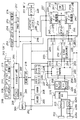
図2は、無線通信装置101の概略構成を示すブロック図である。図2において、201は装置全体の制御を司る中央制御部(MPU)、202はバス(データバスおよびアドレスバス)、203は各種のプログラムが格納されたROM、204はワークエリア等として利用されるRAMである。205はFAXエンジン用のCPU206、ROM及びRAM(図示省略)等を含むマイクロコンピュータ、および画像処理部(図示省略)などから構成されるファクシミリ(FAX)エンジン部、207はFAXエンジン部205のデータバスであり、これらはファクシミリ動作を行うために必要なデバイス(後述の符号208〜216)と接続され、MPU201により制御される。
【0030】
208はカラープリンタ、209はカラースキャナ、210はオペレーションパネル、211はパラレル通信インターフェイスポート、212はパラレル通信インターフェイス用コネクタであり、このパラレル通信インターフェイス用コネクタ212を介してデータ端末103から送信されてきたデータをカラープリンタ208で印刷したり、カラースキャナ209で読取った画像をパラレル通信インターフェイス用コネクタ212を介してデータ端末103に送信したりすることができる。
【0031】
213はFAXモデム、214はハンドセット、215はスピーカ、216は保留メロディ音等を発する音源であり、これらはFAXエンジン部205により制御されると共に、アナログスイッチ217と接続されている。そして、このアナログスイッチ217を経由して音声またはファクシミリのアナログデータがPHSベースバンド処理部239へ送られ、デジタル信号に変換されて、ISDN107に送出される。218は共有レジスタであり、FAXエンジン部205のデータバス207に接続されたデバイスとMPU201のデータバス202に接続されたデバイスとの間でデータを授受する際に使用される。
【0032】
219はRS232Cコントローラ、220はRS232C用のドライバ/レシーバ、221はRS232Cコネクタであり、これらはデータ端末103の通信ポートと接続され、データ端末103がISDN107との間で送受信するデータのインターフェイスとして機能する。なお、本システムにおいてはRS232Cを用いているが、USB(Universal Serial Bus)、IEEE(the Institute of Electrical andElectronic Engineers,Inc)1394、IrDA(Infrared Data Association)、ホームバス等の通信インターフェイスを用いることも可能である。
【0033】
222はISDN107のU点と接続するモジュラコネクタ、223はDSU(Digital Service Unit)であり、局交換機との間で授受されるデータをTTLレベルの信号に変換するものである。224aはISDN107のS/T点に接続する端末とバス接続するモジュラコネクタ、224bはトランス、224cはドライバ/レシーバであり、ISDN107のS/T点に接続する機能を持つISDN端末との間で授受するAMI(AlternateMarkInversion)符号のデータとTTLレベル信号との変換処理を行うことで、複数のISDN端末をバス接続して使用できるようにするものである。
【0034】
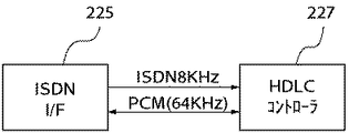
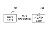
225はISDN107のT点インターフェイス部であり、ISDN107のレイヤ1〜レイヤ3までの制御を行い、ISDN107のBチャネルのデータの入出力機能を有している。226はエコーキャンセラであり、ISDN107で発生したエコーを除去する。227はHDLC(High−level Data Link Control)コントローラであり、ISDN107を介して授受するHDLCフォーマットのデータの組立/分解処理を行う。228はPIAFSコントローラであり、無線データ伝送プロトコル(PIAFS)フォーマットのデータの組立/分解処理を行う。229は第1のポートスイッチであり、5−2切替えスイッチ230を有し、MPU201の制御の下に、ISDN107のB1チャネルとB2チャネルで伝送するデータの切替え処理を行う。232はエコーキャンセラ制御信号であり、エコーキャンセラの動作モード設定やエコーキャンセラ動作のオン/オフ制御を行う。
【0035】
233は第2のポートスイッチであり、2−1切替スイッチ231,234,235を有し、MPU201の制御により、第1のポートスイッチ229に接続するデータの切替え処理を行う。236はI.460規格に基づくデータ変換処理を行うI.460変換部であり、32Kbps/64Kbpsの伝送速度変換処理を行うと共に、PHSエンジン部237からのPIAFSデータを、スルーモードでPIAFSコントローラ228へ切替える処理を行う。
【0036】
上記のPHSエンジン部237は、PHS制御用のCPU238と、音声コーデック部、無線伝送フレームの組立/分解部、変復調部などから構成される2つのPHSベースバンド処理部239,240と、高周波ユニット241と、アンテナ242等により構成されている。PHSエンジン部237は、アナログスイッチ217を介して入出力されるアナログ音声、ファクシミリデータをPCM(Pulse Code Modulation)データに変換すると共に、PHS電話機102,104との間で2チャネルの32KbpsのADPCM(Adaptive Differrential Pulse Code Modulation)の無線音声/データ伝送を行うことを可能にする。なお、本システムにおいては2系統のPHSベースバンド処理部239,240を有しているが、1つのベースバンド処理部により複数スロットを制御することも考えられる。
【0037】
次に、主な信号の機能を説明する。243はMPU201とFAXエンジン部のCPU206の間のシリアル通信用の信号線、244はMPU201とPHSエンジン部205のCPU238との間のシリアル通信用の信号線である。245と246はアナログスイッチ217とPHSエンジン部237を接続するアナログ信号用の信号線であり、この信号線のアナログ信号は、それぞれPHSベースバンド処理部239、PHSベースバンド処理部240内のPCMコーデックによりPCM信号に変換されるとともに、ADPCMコーデックにより32Kbpsの音声データに変換され、所定のフレームに構成されてRFユニット241を介して送信される。
【0038】
247はアナログ信号線245からのアナログ信号をPCM変換した64Kbpsのデータ用の信号線、248は第1の無線スロットで通信する64Kbpsのデータ用の信号線、249はアナログ信号線246からのアナログ信号をPCM変換した64Kbpsのデータ用の信号線、250は第2の無線スロットで通信する64Kbp5のデータ用の信号線である。信号線248、250のPCM変換された64Kbpsのデータは、ベースバンドIC(PHSベースバンド処理部239,240)内のADPCM−PCMトランスコーダにより32Kbpsの音声データ信号に変換されて、RFユニット242を介して送信される。251は非制限デジタル通信で使用する32Kbpsのデータ用の信号線であり、ISDN107のBチャネルに接続するために、I.460変換部236を介してポートスイッチ229に接続される。
【0039】
252はPHSベースバンド処理部239と接続されるPCM音声データ用の信号線、253はPHSベースバンド処理部240と接続されるPCM音声データ用の信号線、254、255はI.460変換部236と接続される非制限デジタルデータ用の信号線であり、それぞれスイッチ231、PIAFSコントローラ228に接続される。256はPIAFSコントローラ228に接続される64Kbpsのデータ用の信号線、257はHDLCコントローラ227に接続される64Kbpsのデータ用の信号線である。258はISDN107のB1チャネルで伝送される64Kbpsのデータ用の信号線、259はISDN107のB2チャネルで伝送される64Kbpsのデータ用の信号線である。
【0040】
260はISDN107から抽出した8KHzと64KHzのクロックを供給するための信号線であり、信号線258、259、247、248、249、250上の信号は、これらのクロックに同期して転送される。261はPHSエンジン部237から出力される8KHzと32KHzのクロックを供給するための信号線であり、信号線251上の信号は、8KHzと32KHzに同期して転送される。
【0041】
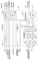
図3は、PHSエンジン部237の詳細な構成を示すブロック図である。図3において301と306はスイッチであり、アナログスイッチ217と接続される信号、無線伝送される信号、及びISDNに接続される信号の切替えを行うものである。302と307はアナログ/PCM変換部、303と308はADPCM/PCM変換部、304と309は図9に示す無線伝送フレームの組立/分解を行うTDMA組立/分解部、305と310はπ/4シフトQPSK(Quadrated Phase Shift Keying)変調/復調部である。311はマルチプレクサであり、無線データ通信を行う際に使用するPHSベースバンド処理239,240を選択するものである。
【0042】
ベースバンド処理部239,240の内部では、CPU238の制御によりスイッチ301,306を切替え、状況に応じてさまざまにデータ伝送経路を切替える切替処理が行われる。例えば、ハンドセットを使ってISDN107経由で通話を行う場合には、アナログスイッチ217から出力されたアナログ信号245は、アナログ/PCM変換部302においてPCM符号に変換されて、データ線247に出力される。一方、ハンドセットと無線電話機の間で通話を行う場合には、アナログ/PCM変換部302でPCM符号に変換された音声データは、スイッチ301でADPCM/PCM変換部303に入力されてADPCM符号に変換された上で、TDMA組立/分解部304により無線フレームに組立てられ、QPSK変調/復調部305にて変調された後に、無線回線に送信される。また、無線電話機からの音声データをISDN107に送出する場合には、信号線247がADPCM/PCM変換部303と接続される。
【0043】
312は位相差に応じた幅のパルスを出力する位相比較器、313はKカウンタ、314はインクリメント/ディクリメント回路、315は分周回路であり、これらデバイスによって構成されたDPLL(Digital Phase−Lock Loop)により、ISDN107から抽出した8KHzクロック(ISDM8K260)に同期した±5ppm精度の384KHzクロック316を生成している。生成した384KHzクロック316およびRFユニット241のTCXOからの±3ppm精度の19.2MHzクロック318を基準にして、PHSベースバンド処理部239,240は動作している。
【0044】
すなわち、PHS電話機102,104とISDN107との間でデータ(PCM符号化された音声を含む)の送受信を行う場合、データのオーバーラン、アンダーランを防ぐために、ISDN回線とPHS無線回線が同期して動作することが必要となる。その一方で、PHS無線回線の同期タイミング精度は±5ppm以内という高い精度が求められる。ISDN107から抽出される同期タイミングクロック(ISDN8K)の精度は±5ppm以内であるため、上記の位相比較器312などから構成されるDPLLによって、ISDN107に同期した8KHzクロック(ISDN8K)260に同期した384KHzクロックを生成し、PHSベースバンド処理部239,240を動作させる必要がある。そこで、PHSエンジン部237は、次のようなDPLLの動作を行う。
【0045】
すなわち、DPLLで生成された出力クロックを分周した8KHzクロック317と、ISDN107に同期した8KHzクロック(ISDN8K)260が位相比較器312に入力される。そして、位相比較器312は、位相比較結果に応じて、ISDNクロック(ISDN8K)260の位相が進んでいれば5Vのパルスを、位相が遅れていれば0Vのパルスを、Kカウンタ313に出力する。
【0046】
Kカウンタ313は、アップカウンタとダウンカウンタから構成されており、位相比較器312からの位相情報に基づいてRFユニット241からの19.2MHzの基準クロックをアップカウント、またはダウンカウントして、CA(キャリー)、またはBO(ボロー)を出力する。このキャリー、ボローは、インクリメント/ディクリメント回路314に入力され、RFユニット241からの19.2MHzの基準クロックを2分周すると共に、キャリーを受信した場合は1/2周期のパルスを上記2分周したクロックに挿入して出力し、ボローを受信した場合は1/2周期分のパルスを上記2分周したクロックから削除して出力する。
【0047】
分周回路315は、インクリメント/ディクリメント回路314から出力されるクロックを分周することで、装置内部でのバーストタイミンダの基準クロック316と、ISDN107からの網同期信号(ISDN8K)との位相比較を行うための8KHzの内部基準クロック317を生成する。
【0048】
なお、内部クロックモードの場合、ISDN8Kのクロックは入力されず、インクリメント/ディクリメント回路314では、RFユニット241から入力される基準クロックをビットの増減を行わずにそのまま2分周して、分周回路315へ出力する。そして、分周回路315では、2分周された基準クロックをそのまま再度分周し、内部でのバーストタイミングの基準クロック316を生成する。また、内部クロックモードの場合は、8KHzの内部基準クロック317も使用しない。
【0049】
さらに、DPLLは、例えばSN54/74LS297を用いて構成することができる。また、位相比較器312、Kカウンタ313、インクリメント/ディクリメント回路314、分周回路315は公知である。さらに、本実施形態では、QPSK変調/復調部を複数有する構成となっているが、TDMA組立/分解部304,309が複数のスロットに対応していれば、1つのQPSK変調/復調部で構成することも可能である。
【0050】
図4、図5は、図2に示したスイッチ230の詳細な構成を示すブロック図である。図4、図5において、401と402はデコーダ、403と405はORゲート、404と406はANDゲートである。
【0051】
図4は、スイッチ230のうち、ISDN107から受信したB1チャネル、B2チャネルのデータを、PHSエンジン部237に通じる3本の信号線252,253,254、HDLCコントローラ227、PIAFSコントローラ228のうちのいずれかに接続するための構成要素を示している。
【0052】
スイッチ230に割当てられたアドレスにMPU201が所定の値を書込むと、スイッチ230は、その値をデコーダ402によりデコードすることにより、信号線258,259を接続すべき相手に対応する信号線252,253,254,256,257に通じるORゲート403にのみL(0V)を出力し、他のORゲ−ト404にはH(5V)を出力する。従って、選択されたORゲート403からのみ信号線258,259のデータがANDゲート404に入力され、結果として信号線258,259がそれぞれ5本の出力信号線のうちの1本と接続されることとなる。
【0053】
図5は、スイッチ230のうち、PHSエンジン部237に接続された3本の信号線252,253,254、HDLCコントローラ227、PIAFSコントローラ228のいずれかを、ISDN107のB1チャネル、B2チャネルの送信信号線に接続するための構成要素を示している。
【0054】
スイッチ230に割当てられたアドレスにMPU201が所定の値を書込むと、スイッチ230は、その値をデコーダ402によりデコードすることにより、ISDN107のB1チャネル、B2チャネルの送信信号線にそれぞれ接続すべき信号線252,253,254,256,257に対応する2つのORゲート405にのみL(0V)を出力し、他のORゲ−ト405にはH(5V)を出力する。これにより、5本の信号線のうち1本はISDN107のB1チャネルに通じる信号線258に接続され、1本はISDN107のB2チャネルに通じる信号線259に接続されることとなる。
【0055】
図6は、ポートスイッチ233の詳細な構成を示すブロック図である。図6において、501は選択回路(マルチプレクサ)502,503,510,511を制御する信号を生成するデコーダ、502はシリアルデータをアナログ信号に変換するか、或いは無線回線に出力するかを切替えるための選択回路であり、デコーダ501を介してMPU201により制御される。この選択回路502の出力は、PHSエンジン部237にデータ247(249)、またはデータ248(250)として入力される。逆に、PHSエンジン部237から出力されるデータ247(249)、または248(250)は、マルチプレクサ503により、アナログ信号をPCM信号に変換するか、或いは無線部からの信号をPCM信号に変換するかが選択され、網からの同期信号260に同期してデータ信号252としてポートスイッチ229に出力される。
【0056】
選択回路511は、デコーダ501の制御により、無線回線からのデータをISDN107に出力するのか、或いはPIAFSコントローラ228に出力するのかを選択する。510はPIAFSコントローラ228からの32KbpsのPIAFSフレーム信号を無線回線に出力するのか、或いはISDN107からのPIAFSフレーム信号を無線回線に出力するのかを切替えるためのデマルチプレクサであり、デコーダ501を介してMPU201により制御される。デマルチプレクサ510の出力251は、PHSエンジン部237に入力される。逆に、選択回路511は、PHSエンジン部237から出力されるデータ(32KbpsのPIAFSフレーム信号)をそのままPIAFSコントローラ228へ出力するのか、或いはI.460変換してISDN107に出力するのかを切替えるための選択回路であり、デコーダ501を介してMPU201により制御される。
【0057】
PHSエンジン部237からの信号をISDN107に出力する場合は、I.460変換部236により、32Kbps−64Kbps変換処理が行われる。この際、I.460変換部236内のパラレル/シリアル変換部507、シリアル/パラレル変換部509は、8KHz、32KHzのクロックタイミングで動作する。
【0058】
32KHzのクロックに同期してPHSエンジン部237から入力されるデータは、シリアル/パラレル変換部509において、4ビットのパラレルデータに変換されると共に、4ビットのダミービットが挿入されて、8ビットのデータとしてF1FO508に入力される。パラレル/シリアル変換部507は、F1FO508内の8ビットのデータを、1SDN107より作成される64KHzのクロックに同期して、シリアル信号として取出してISDN107に出力する。
【0059】
また、ISDNインターフェイス225より入力されるPCMデータを、64KHzのクロックに同期して、シリアル/パラレル変換部504でパラレルデータに変換し、F1FO505に書込む。パラレル/シリアル変換変換部506では、所定の4ビットを削除し、PHSエンジン部237からの32KHzのクロックに同期して、シリアルデータとしてPHSエンジン部237ヘ送信する。また、PHSエンジン部237からの信号をPIAFSコントローラ228に出力する場合は、データおよびクロックを選択回路510,511で切替える。
【0060】
PHSエンジン部237からI.460変換部に入力される同期信号(8KHz)261は、PHSエンジン部237のクロックがISDN107に同期している場合は、位相および立上りがISDN107からの同期信号(ISDN8KHz)260に完全に同期している。本システムがISDN107に接続されていない場合は、I.460変換部236は使用されず、本パスを通過するデータは全てPIAFSデータであるとして同期信号261、およびデータ251をPIAFSコントローラ228に転送する。
【0061】
図7は、アナログスイッチ217の詳細な構成を示すブロック図である。図7において、601はアナログスイッチ217を制御するレジスタであり、データバス202を介してMPU201によってデータが書込まれる。602はデコーダであり、レジスタ601に書込まれたデータをデコードして、アナログスイッチ603〜614と、n対nアナログスイッチ615,616を制御する信号を発生する。
【0062】
アナログスイッチ603〜614は、入力ピン、出力ピン、制御ピンから構成され、制御ピンがロウレベルの時には入力ピンと出力ピンが接続され、制御ピンがハイレベルの時には入力ピンと出力ピンが切離される。n対nアナログスイッチ615、616は、ベースバンド処理部239,240、音源216、FAXモデム213内の信号出力212を、ハンドセット214、スピーカ215のどちらに接続するかの制御を行うものである。
【0063】
ベースバンド処理部239,240に送られるデータは、アナログスイッチ603〜614により、モデム213からの出力信号、ハンドセット214から入力される音声信号、音源216からのメロディ音の中から、MPU201の制御に基づいて選択される。具体的には、FAX通信を行う場合にはFAXモデム213が接続され、ハンドセット通話が行われる場合にはハンドセット214が接続され、保留中は音源216が接続される。
【0064】
逆に、FAX通信中には、ベースバンド処理部239,240から出力されるデータは、FAXモデム213に入力され、通話中には、n対nアナログスイッチ615,616を切替えて、ベースバンド処理部239,240から出力される音声信号をハンドセット214やスピーカ215に出力することが可能である。保留中には、音源216から出力される信号をハンドセット214やスピーカ215に接続し、FAXモデム213内の通話録音部に録音された音声を聞く場合には、FAXモデム213から出力される信号をハンドセット214やスピーカ215に接続して使用する。
【0065】
このようにして、動作モードに応じて、複数種類のアナログ信号を切替えてベースバンド処理部239,240に入力し、ISDN107や無線回線上で通信を行うことができる。アナログスイッチ603〜614は公知の74HC4053等のアナログスイッチ、または市販のクロスポイントスイッチを用いて構成することが可能である。
【0066】
図8は、本システムにおけるU点およびT点のハード構成を示すブロック図である。U点インタフェースは、ISDN107からの直流成分を切離すトランス、および内部に送受信用バッファを有し、ピンポン伝送(TCM:Time Compression Multiplexing Transmission)方式により、2線の平衡ケーブルを用いてISDN107との同期を取りながら144Kbpsの双方向の伝送を行うと共に、T点側に対してはAMI(Alternated Mark Inversion)符号により、送信・受信とも2線を使用し合計4線のインターフェイスでデータ送受信を行う。
【0067】
ピンポン伝送のフレームは、20ワードの情報とフレームビット、監視ビット、直流平衡ビットより構成される。本フレームは一般的なので説明を省略する。AMI符号に関しては、INSネットサービスのインターフェイスにより規定され、公開されているので説明を省略する。
【0068】
U点インターフェイスは、局交換機と本システム間を2線のメタリックケーブルでピンポン伝送方式により双方向の伝送を可能にするためのトランス801、ピンポン伝送におけるバースト送受信の切換を行うスイッチ802、バースト送受信のタイミングを生成するバースト同期回路803、受信したパルスの反射成分を取り除きケーブルの周波数特性を一定に保つための等化回路804、フレーム同期およびバースト同期を行うためのタイミング信号をAMI符号から生成するためのTIM805、局交換機からピンポン伝送で送られてきた2B+Dのデータを一旦バッファリングして、AMI符号化されたベーシックインターフェイスのフレーム構成でT点回路に出力する受信バッファメモリ部806、T点回路からのAMI符号化されたベーシックインターフェイスのフレームを分解して、2B信号およびD信号をバッファするための送信バッファメモリ807、及び送信バッファメモリ807に記憶しているデータを局交換機に送信するために、2B+Dのデータを所定のフレームに組立て送信するためのラインドライバ808、及びISDN107からのリバース信号を検出するリバース検出回路816により構成されている。
【0069】
T点インターフェイスは、U点からのAMI符号を受信し、受信したフレーム中のフレームビットを基に2B+Dチャネルのデータを分解し、Bチャネルの受信データを通話路へ出力する。また、受信したAMI符号から内部で位相の同期をとり、通話路に対して同期信号を送出するまた、送出した同期信号に同期して受信される通話路上のデータを、AMI符号のフレームに組立てて、U点インターフェイスに送出する。
【0070】
T点インターフェイスは、U点との切離しを可能とするためのライントランス809、ベーシックインターフェイスフレームを送受信するためのドライバ810、U点より受信するAMI符号化された信号を分解しBチャネルおよびDチャネル毎にメモリにバッファするフレーム分解部811、受信したAM1符号化された信号からシステムの通話路で使用する基準クロック(64kHzおよび8KHz)を生成するDPLL回路812、後述するBchインターフェイスからのデータ信号、またはCPUインターフェイスからのデータ信号を、U点に送信すべくAMI符号化されたベーシックインターフェイスフレームに組立てるフレーム組立部813、DPLL回路812で生成される基準クロックに基づいて、PCM送受信信号を同期信号260に同期させてフレーム組立部813に送出すると共に、フレーム分解部811で分解されたデータを、同期クロック260に同期させて通話路に出力するBchインターフェイス814、MPU201とバスにより接続されてT点回路の制御を行うMPUインターフェイス815により構成されている。
【0071】
DPLL回路812は、内部に波形変換回路を有しており、AMI符号信号を正負2つのコンパレータにより2つのRZ(Return−to−Zero)信号に変換し、この2つの信号を論理和により合成することで192KHzの基準クロックを生成する。さらにDPLL回路812は、通話路の基準同期信号として、この192KHzのクロックを24分周することにより8KHzのクロックを生成し、3分周することにより64KHzのクロックを生成する。
【0072】
本システムがISDN107に接続されている場合は、DPLL回路812がロックしているか否かを、ISDN107からのクロックによりCPUインターフェイス202を介して知ることができる。
【0073】
なお、本実施形態においては、同期信号は8KHzと64KHzで構成されているが、この他、ISDN107からのクロックを同期用の信号として直接使用する場合には、192KHz、384KHzの信号と8KHzの信号の組合せたものを、同期信号として用いることも可能である。
【0074】
図9は、PHS無線伝送フレームフォーマットを示した図であり、図9(a)は無線リンク確立時に使用するSCCH(個別セル呼び出し)フレーム、図9(b)はPCH(Paging Channel:一斉呼び出しチャネル)フレーム,図9(c)は通常データの通信に使用するTCH(Traffic Channel:情報チャネル)、FACCH(Fast Associted Control Channel:高速付随制御チャネル)などのフレームである。
【0075】
図10は、無線データ伝送プロトコル(P1AFS)で使用するフレームフォーマットを示した図であり、図10(a)はプロトコルの選択及びフレーム同期を確立するために送受信されるネゴシエーションフレーム、図10(b)は通信中のフレーム再同期を取るために送受信される同期フレーム、図10(c)は制御情報を送受信するための制御フレーム、図10(d)はユーザデータを送受信するためのデータフレームである。
【0076】
P1AFSによるデータ通信を行う際には、まずネゴシエーションフレームを用いてインバンドネゴシエーション、フレーム同期確立、応答遅延時間測定などを行い、次に制御フレームにより通信パラメータの設定を行い、データフレームによるデータ通信を開始する。
【0077】
図11は、PPP(Point to Point Protocol)のフレームフォーマットを示したである。図11において、フラグはフレームの始まりと終わりを示す01111110のパターン、アドレスは11111111の固定パターン、制御は00000011の固定パターン、プロトコルは使用するネットワーク層プロトコルの種別を示す2バイトのデータ、データはPPPの制御データやユーザデータなどを含む可変長の伝送情報、FCS(Frame Check Sequence)はデータ誤り検出符号である。
【0078】
次に、本無線通信装置101における種々の動作モードでの動作とデータの流れを、図12〜図26を用いて説明する。なお、図12〜図20のフローチャートに対応するプログラムは、プログラムメモリ、ROM203、CPU238に内蔵されたROMに格納されている。
【0079】
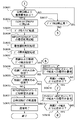
[電源投入時のMPU201による初期化処理]
本無線通信装置101に電源が投入されると、MPU201は、図12のフローチャートに示す動作を行う。
【0080】
すなわち、本体へ電源が供給されると、MPU201は、RAM204のワークエリアを確保すると共に、各構成要素(IC)の初期化処理を行う(ステップS0001)。初期化処理が終了すると、U点(DSU)223にて検出されたISDN107からのリバース信号を基に、ISDN107との接続を確認する(ステップS0002)。ISDN107との接続が確認できた場合、T点インターフェイス225においてISDN107との同期が確立しているかを確認する(ステップS0003)。同期が確立している場合には、正常な64KHzと8KHzが出力され同期を示すビットが立つ。
【0081】
ISDN107との同期が取れていることが確認できた場合は(ステップS0004)、T点インターフェイスより通話路用クロック260が出力される(ステップS0005)。通話路用クロックが出力されると、MPU201は、PHSエンジン部237に対して初期化開始命令を送り、出力クロックに同期した処理を行うよう指示する(ステップS0006)。その後、PHSエンジン部237から無線部の初期化完了信号を受信すると(ステップS0007)、無線回線への発着信が可能であるとして、同期が確立した旨を表示部に表示すると共に、待機処理を始める。
【0082】
上記の表示処理としては、LEDの点灯またはLCD表示部への表示が考えられる。また、同時に、同期が確立した旨を音源216により音声ガイダンスで通知することも考えられる。この場合は、アナログスイッチ217によりスイッチして、音源216に内蔵された音声ガイダンス信号をスピーカ215へ出力する。
【0083】
ISDN107との接続が完了していない場合は(ステップS0002)、PHSエンジン部237に対してPHSエンジン部237の内部クロックによる処理を行うように命令を送信する(ステップS0009)。そして、PHSエンジン部237より初期化完了を受信した場合は(ステップS0010)、PHSエンジン部237は、内線通信のみ可能であるとして非同期時の処理中である旨の表示を行い、待機時の処理を行う。この表示処理としては、LEDの点灯またはLCD表示部への表示が考えられる。また、同時に、同期が確立していない旨を音源216により音声ガイダンスで通知することも考えられる。この場合は、アナログスイッチ217によりスイッチして、音源216に内蔵された音声ガイダンス信号をスピーカ215へ出力する。
【0084】
本処理においてISDN107との接続が完了しているか否かは、U点インターフェイスにてリバースを検出することにより確認できる。また、電源投入直後は、回線への接続がなされていない場合が多いので、接続確認処理の頻度を多くしている。
【0085】
[電源投入時のCPU238による初期化処理]
本無線通信装置101に電源が投入されると、PHSエンジン部237のCPU238は、図13、図14のフローチャートに示す動作を行う。
【0086】
すなわち、PHSエンジン部237に電源が供給されると(ステップS0101)、CPU238は、内部の設定、およびメモリのワークエリアの設定を行い、網同期、すなわちISDN107から抽出したクロックによるISDN107との同期により無線部を初期化する初期化要求信号を、本体側のMPU201から受信したか否かを判断する(ステップS0102)。その結果、上記の初期化要求信号を受信した場合は、ISDN107とのデータ送受信が可能であるとして、T点インターフェイスより出力される8KHzの信号を基に伝送用のクロックの同期を取り、上記網同期を取るための処理をPHSベースバンド処理部239,240にて実行させる(ステップS0103)。そして、PHSベースバンド処理部239,240にて網同期が取れたか否かを判別する(ステップS0104)。その結果、網同期が取れた場合は、報知信号を出力するためにキャリアを検索する(ステップS0105)。この時、PHSベースバンド部239,240は、自営標準で規定されている制御用のチャネル12chおよび18chを用いてキャリアセンスを行う。この時のスロットのタイミングは、ISDN107からの8KHzに同期するよう決められている。
【0087】
また、網同期により動作中の基準スロットにおいて送信不可であると判断した場合、CPU238は、網同期を一旦解除する(ステップS0110)。この解除処理は、網同期状態において、送信スロットを移動した場合、網同期が外れるために行われる。網同期を解除した後、送信に使用するスロットを送信可能なスロットヘ移動する(ステップS0111)。スロットの移動が完了したことを検出すると(ステップS0112)、再度、PHSベースバンド部239,240を網同期で動作するように設定し(ステップS0113)、網同期の確立を確認する(ステップS0103)。
【0088】
キャリア検索の結果、所定のスロットにて報知信号を送出し得ると判断した場合は(ステップS0106)、LCCH(Logic Control Channel)を用いて所定のタイミングで報知信号を送信する(ステップS0107)。そして、CPU238は、MPU201に対して網同期による初期化が完了したことを通知して、網同期による通信を行う(ステップS0108)。この処理中に、MPU201から網との同期の終了が通知されるのを監視し(ステップS0109)、網との同期の終了が通知されない場合は、通常の処理を継続する。
【0089】
MPU201から網との同期の終了が通知された場合は、図14のステップS0201以降の内部クロックモードで動作するための処理へ移行する。なお、ステップS0102にて、無線部を網同期により初期化する初期化要求信号を受信しないと判断された場合、及びステップS0104にて、PHSベースバンド処理部239,240で網同期が取れなかったと判断された場合も、ステップS0201以降の内部クロックモードで動作するための処理へ移行する。
【0090】
[内部クロックモードで動作時の処埋]
CPU238は、MPU201から内部クロックモードによる動作命令を受信すると(ステップS0201)、PHSエンジン部237に対して内部クロックモードによるキャリア検索を開始させる(ステップS0202)。そのキャリア検索の結果、報知信号用のスロットおよび周波数を獲得できなかった場合は(ステップS0203)、送信可能なスロットヘの移動処理を行う(ステップS0207)。なお、内部クロックモードにおいては、スロットの移動は自由である。スロットの移動が完了すると(ステップS0208)、再度キャリアを獲得するための処理を行う(ステップS0203)。
【0091】
キャリア検索の結果、所定のスロットにおいて報知信号送出が可能であると判断した場合は(ステップS0203)、LCCHを用いて、所定のタイミングで報知信号の送信を開始する(ステップS0204)。報知信号の送信を開始すると、CPU238は、MPU201に対して内部クロック動作モードによる初期化が完了したことを通知し、内部クロックでの通信を行う(ステップS0205)。この処理中に、MPU201から網同期開始の通知がなされるのを監視する(50206)。網同期開始の通知がなされない場合は、通常の処理を継続する。網同期開始の通知がなされた場合は、前述の網同期モードで動作するための処理へ移行する。
【0092】
[PHS電話機との音声通信動作]
無線データ端末(PHS電話機102)が、ISDN107を介して音声通信動作を行う場合、本無線通信装置101のMPU201は、図15のフローチャートに示す動作を行う。
【0093】
すなわち、PHS電話機102のキー操作によってダイヤルがなされると、無線通信装置101とPHS電話機102の間で、上記図15に示すフローチャートに従って発信処理が行われる。
【0094】
具体的には、まず、PHS電話機102は、無線通信装置101に対して、無線リンクのリンクチャネル確立要求信号をSCCHチャネルにより送信する。無線通信装置101においては、PHSエンジン部237内のCPU238がアンテナ242、高周波ユニット241、ベースバンド処理部239,240を介して無線リンクチャネル確立要求信号を受信すると(ステップS0301)、PHS電話機102に対して、リンクチャネル割当メッセージを送信する。
【0095】
PHS電話機102から無線リンク確立要求信号を受信しない場合は、MPU201は、U点インタフェース223およびT点インタフェース225を監視することにより、デジタル回線の状態を監視する(ステップS0311)。デジタル回線の状態が正常な場合は、PHS電話機102からのリンク確立要求信号を監視する(ステップS0301)。デジタル回線が正常ではないと判断すると、回線異常時の処理を行う。本処理は、特にISDN107との接続が絶たれた場合や、ISDN107との網同期が確立しなくなった場合に行う。
【0096】
PHS電話機102は、無線通信装置101からリンクチャネル割当てを受けると、呼設定メッセージを送信する。呼設定メッセージを受けたCPU238は、呼設定確認メッセージをPHS電話機102に送り、呼設定確認メッセージを受けたPHS電話機102は、無線管理、移動管理関連メッセージをCPU238と授受した後、付加情報メッセージを送信する。
【0097】
CPU238は、付加情報メッセージを受信すると、ISDN107ヘの発信要求があったことを、シリアル通信データ244によりMPU201に通知する(ステップS0302)。発信要求を受けたMPU201は、ISDNインターフェイス225の発信処理を起動する(ステップS0303)。ISDNインターフェイス225は、MPU201にてメモリ204に格納されたレイヤ3のメッセージをISDN107へDMA転送し、ISDN107との間でメッセージを授受する(ステップS0304)。ISDNインターフェイス225は、ISDN107から応答メッセージを受信すると(ステップS0305)、MPU201に割込みをかけ、MPU201は、CPU238に対して応答通知を行うよう指示し、その指示を受けたCPU238は、ベースバンド処理部239,240などを介して、PHS電話機102に応答メッセージを送信し(ステップS0306)、それ以降、PHS電話機102と無線通信装置101の間で通話チャネルが接続される。
【0098】
そして、MPU201は、呼設定メッセージの授受で音声通信であることを確認している場合は、各種ポートスイッチを切替えて、音声通信を行うための処理へ移行する(ステップS0307)。同時に、MPU201は、PHS電話機102の通話チャネルとISDN107のBチャネルを接続するように、第1のポートスイッチ229、第2のポートスイッチ233を切替える。本実施例ではPHS電話機102で送受信する音声は、PHSベースバンド処理部239で送受信されてデータ線247で伝送されるので、第2のポートスイッチ233のスイッチ234を制御して、データ線247をデータ線252に接続する。さらに、スイッチ234が接続されているデータ線252がISDN107のB1チャネルのデータ線258に抜続されるように、第1のポートスイッチ229を切替える(ステップS0308)。
【0099】
さらに、PHS電話機102で音声通信をする場合、無線伝送フレーム組立/分解処理による遅延の影響で回線エコーが発生するため、エコーキャンセラ226を動作させる必要がある。そこで、MPU201は、エコーキャンセラ226がエコーキャンセル動作を開始するように、第1のポートスイッチ229を介して所定の設定を行う(ステップS0309)。
【0100】
以上の処理により、PHS電話機102から入力された音声は、PHSベースバンド処理部239で受信され、受信したPCMデータ(音声データ)は、エコーキャンセラ226、ISDNインターフェイス225、DSU223、コネクタ222を介してISDN107に送信される。ISDN107から受信した音声データも、全く同様の経路でPHS電話機102に送信される。
【0101】
次に、音声通話時の同期信号およびデータ信号の流れを図21を参照しながら説明する。ISDNインターフェイス225において網同期が確立すると、ISDN107のクロックに同期した同期信号ISDN8KHzが出力される。また、このISDN8KHzに同期してデータ送受信を行うためのクロック(64KHz)も出力される。PCM信号は、このISDN8KHzと64KHzに同期して各デバイス(IC)間で入出力される。
【0102】
音声通信時には、ISDNインターフェイス225から出力されるISDN8KHzと64KHz信号、およびPCM音声データが、PHSベースバンド処理部239へ出力される。PHSベースバンド処理部239では、ISDN8KHzに基づいてDPLLにより同期クロックを作成し、このクロックを基に無線の送受信処理を行う。受信した音声データは、ADPCM/PCM変換され、ISDN8KHzおよび64KHz信号に同期して、ISDNインターフェイス225ヘ出力される。
【0103】
[データ端末106によるPIAFS通信]
次に、データ端末106からのPIAFSによるデータ送信動作を、図15、図22を参照しながら説明する。
【0104】
図1に示したように、データ端末106が、PIAFSカード105、PHS電話機104、及び本無線通信装置101を介してISDN107に接続され、PIAFSデータの通信を行うことのできる相手とデータ通信を行う場合、データ端末106の通信アプリケーションソフトが起動し、データ端末106に接続されたPIAFSカード105に対して発信要求が出される。すると、PIAFSカード105は、PHS電話機104に対して発信要求を転送し、発信要求を受けたPHS電話機104は、上記のPHS電話機102と同様に、無線通信装置101に発信を行い、無線通信装置101はISDN107に対して発信を行う(ステップS0301〜ステップS0304)。ただし、この場合には、呼設定メッセージ内の情報は、32Kbpsの非制限デジタルデータに設定されている。
【0105】
ISDN107からの応答を受けると(ステップS0305)、PHS電話機104に対して応答メッセージを送信し(ステップS0306)、PHS電話機104はPIAFSカード105を介して、相手が応答したことをデータ端末106に通知する。一方、無線通信装置101は、先の呼設定メッセージ内の情報が32Kbpsの非制限デジタルデータに設定されているので、送信データはPIAPSデータであると判断し(ステップS0307)、第1のポートスイッチ229内のスイッチ230と、第2のポートスイッチ233内のスイッチ231を切替える。
【0106】
具体的には、データ線251の信号がI.460変換部236を経由してデータ線254に接続されるように、スイッチ231を切替え、データ線254がデータ線258に接続されるようにスイッチ230を切替える(ステップS0312)。さらに、エコーキャンセラ226は、スルーモードに設定されている(ステップS0313)。以上の手順でデータ通信チャネルが接続される(ステップS0314)。
【0107】
通信チャネルが確立された後は、まず、データ端末106と相手端末との間でPIAFSプロトコルのネゴシエーションが行われる。PIAFSカード105にて送信されるPIAFSネゴシエーションフレームは、PHS電話機104を介して無線通信装置101のPHSベースバンド処理部239で受信される。受信された32Kbpsデータは、データ線251を介してI.460変換処理部234で64Kbpsに変換された上で、第1のポートスイッチ229、エコーキャンセラ226、ISDNインターフェイス225、DSU223を介してISDN107に送信される。
【0108】
このようにして、ISDN107に接続された相手との間でPIAFSデータの送受信を行えるようになるので、PIAFSプロトコルに従った所定のネゴシエーションにより、相手とのPIAFSリンクを確立した上で、データの送受信が開始される。データ端末106が送信するデータ(PPPプロトコルフォーマット)は、PIAFSカード105によりPIAFSヘッダとトレーラが付加され、上記ネゴシエーションフレームと同様の流れで相手に送られ、相手においてP1AFSヘッダとトレーラが削除されて、データフィールドに格納されたPPPプロトコルフォーマットのデータのみが取出され、上位ソフトにより処理される。
【0109】
この際、送信するデータは、図10に示すPIAFS無線電送フレームに従ったフレーム構成となっている。また、PHSエンジン部237にて音声通信時に設定されているVOX(Voice Operated Transmission)やレベルの設定は、全て0FFされる。PHS電話機104を介して受信したデータは、全てスルーでデータ信号線251へ出力される。
【0110】
PIAFS通信中の同期信号およびデータ信号は、図22のように流れる。すなわち、音声通話時と同様に、ISDN107と同期したクロックISDN8KHzと64KHz、およびデータ信号が、PHSベースバンド処理部239とI.460変換部236に入力される。PHSベースバンド処理部239では、内部に有するPLL回路により同期クロックを作成し、このクロックを基に無線の送受信処理を行う。さらに、内部で同期が確立した8KHzの同期信号を、PHSベースバンド処理部239からI.460変換部236へ出力する。また、前記8KHzと同期した32KHz信号およびPIAFSデータも同時に出力する。
【0111】
I.460変換部236は、64KHzと32Kzのデータ速度の変換を行う。この際、ISDN8KHzと8KHzは、立上り、および位相が完全に一致している場合もあるが、PCMスロットを用いてPCM信号を多重化している場合は、位相がずれていることも考えられる。なお、PCM信号を多重化している場合は、データ通信に使用するクロックは、64KHzに限らず192KHz、384KHzから2048KHzなどの64KHzを逓倍したクロックにより構成してもよい。
【0112】
[データ端末103による1SDNアクセス動作]
次に、本無線通信装置101において、データ端末103を用いてISDN107をアクセスする場合の、MPU201の動作を図16のフローチャートに従って説明する。
【0113】
データ端末103がISDN107を介して接続された相手とデータ通信を行う場合、データ端末103の通信アプリケーションソフトが起動し、ATコマンドにより発信先番号が送信される。無線通信装置101では、上記コマンドを受信すると(ステップS0401)、データはRS232Cコネクタ221を介してRS232Cコントローラ(シリアル通信コントローラ)219に入力される。RS232Cコントローラ219は、データを受信すると、MPU201に割込みをかけ(ステップS0402)、MPU201は、RS232Cコントローラ219に格納されたデータをRAM204に転送する(ステップS0403)。
【0114】
データ端末103からの発信要求を受信しない場合、MPU201は、U点インタフェース223、およびT点インタフェース225の状態、すなわちデジタル回線の状態を監視する(ステップS0423)。デジタル回線の状態が正常な場合は、データ端末103からの発信要求を監視する(ステップS0401)。デジタル回線が正常でない場合は、回線異常時の処理を行う。MPU20Iは、受信したデータを解析して発信要求であることを認識すると、ISDNインターフェイス225の発信処理を起動する(ステップS0404)。
【0115】
ISDNインターフェイス225は、MPU201にてRAM204に格納されているレイヤ3のメッセージをDMA転送し、ISDN107との間でメッセージを授受する(ステップS0405)。ISDNインターフェイス225は、ISDN107から応答メッセージを受信すると(ステップS0406)、MPU201に割込みをかけ、割込みを受けたMPU201は、相手との接続を認識すると、RS232Cコントローラ219を介して、データ端末103に接続通知を行う(ステップS0407)。さらに、MPU201は、第1のポートスイッチ229を制御し、データ線257とデータ線258を接続する(ステップS0408)。従って、HDLCコントローラ227から出力されたデータは、エコーキャンセラ226、1SDNインターフェイス225、DSU223、コネクタ222を介してISDN107に送信されることになる。
【0116】
この際、データ通信においてはエコーキャンセル処理を行う必要がないため、MPU201は、第1のポートスイッチ229を介してエコーキャンセラ226をスルーモードに設定する(ステップS0409)。このようにして、データ通信チャネルが接続され、データ端末103とISDN107との間でデータ送受信を行うことができるようになる(ステップS0410)。
【0117】
データ端末103は、接続通知を受けることにより、データの送信を関始する。このとき送信するデ−タは、図11に示す非同期PPPに従ったフレーム構成となっている。データ端末103が送信するデータは、前述のATコマンドデータと同様にして、RS232Cコントローラ219を介してRAM204に格納される。すなわち、データを受信すると(ステップS0411)、RS232Cコントローラ219はMPU201に割込みをかけ(ステップS412)、MPU201は、RAM204にデータを転送する(ステップS0413)。
【0118】
格納されたデータは非同期PPPに従っているため、ISDN107に送信する際に使用するHDLCのフラグパターン(01111110)と同一のパターンを含む場合がある。そこで、MPU201は、格納されたデータを読出して、上記フラグパターンがデータ中に現れないようなPPP非同期/同期変換処理を行う(ステップS0414)。
【0119】
具体的には、フラグパターンと同じビット列が現れた時には、コントロールエスケープ(01111101)+フラグパターンの第6ビットを反転したデータ(01011110)に置換する処理を行う。その上で、MPU201は、フラグパターン以外のデータをHDLCコントローラ227に転送し(ステップS0415)、HDLCコントローラ227は、ISDN107から抽出した64KHzクロックに同期したデータ255を第1のポートスイッチ229に送信し、ISDNインターフェイス225を介してISDN107に送信する(ステップS0416)。
【0120】
逆に、ISDN107からデータを受信すると(ステップS0417)、コネクタ222、DSU223、ISDNインターフェイス225、エコーキャンセラ226、第1のポートスイッチ229を介して、受信データをHDLCコントローラ227に入力する。HDLCコントローラ227は、受信データからフラグパターンを検出すると(ステップS0418)、MPU201に対して割込みをかけ、MPU201は、受信データをRAM204に格納する(ステップS0419)。MPU201は、格納されたデータのPPP同期/非同期変換処理を行った上で(ステップS0420)、RS232Cコントローラ219を介して、データ端末103に送信する(ステップS0421)。このようにして、データ端末103によりISDN107を介してデータ通信を行うことが可能となる。
【0121】
図23に有線データ端末(データ端末103)による通信時の同期信号、およびデータ信号の流れを示す。
【0122】
ISDNインターフェイス225から出力される同期信号は、HDLCコントローラ227に直接入力され、この同期信号に同期してデータ端末103は、PCM信号を送受信する。この処理中は、ISDNインターフェイス225でのみ同期が確立していればよく、HDLCコントローラ227は、この同期信号を用いて通信を行うだけである。
【0123】
[データ端末106によるPIAFSデータのPPP送信]
本無線通信装置101において、無線で接続されているデータ端末106により、PIAFSデータの通信を行うことのできない相手とデータの通信を行う場合、MPU201は、図17のフローチャートに示す処理を行う。この場合、相手に対してはPPPデータの形式で送信する必要があるため、無線通信装置101内部でデータ変換処理を行う必要がある。
【0124】
すなわち、データ端末106からデータ送信を行う場合には、データ端末106の通信アプリケーションソフトが起動し、データ端末106に接続されたPIAFSカード105に対して発信要求が出される。PIAFSカード105は、接続されたPHS電話機104に対して発信要求を出し、発信要求を受けたPHS電話機104は、無線通信装置101に発信する。
【0125】
無線通信装置101のPHSエンジン部237は、PHS電話機104からの発信要求を受信すると(ステップS0501)、MPU201に対して割込みをかけ(ステップS0502)、MPU201は、ISDNインターフェイス225の発信処理を起動し(ステップS0503)、ISDN107に対して呼設定メッセージを送信する(ステップS0504)。ただし、この場合は、64Kbpsの同期PPPデータを送信することになるので、呼設定メッセージ内の情報は64Kbpsの非制限デジタルデータに設定されている。PHS電話機104からの発信要求を受信しない場合は、MPU201は、U点インターフェイス223およびT点インターフェイス225の状態を監視することにより、ISDN107(デジタル回線)の状態を監視する(ステップS0505)。デジタル回線の状態が正常であれば、PHS電話機104からのリンク確立要求を監視する(ステップS0501)。デジタル回線が正常ではないときは、回線異常時の処理を行う。
【0126】
ISDN107からの応答を受けると(ステップS0505)、PHS電話機104に対して応答メッセージを送信し(ステップS0506)、PHS電話機104は、PIAFSカード105を介してデータ端末106に相手が応答したことを通知して、通信チャネルが確立される。一方、無線通信装置101は、受信したP1AFSデータを同期PPPデータとしてISDN107に送信するために、第1のポートスイッチ229内のスイッチ230と、スイッチ231を切替える。
【0127】
具体的には、データ線251の信号がI.460変換部236を経由してデータ線255を介してPIAFSコントローラ228の32KbpsのPIAFSデータインターフェイスに接続されるように、スイッチ231を切替えると同時に、HDLCコントローラ227の64Kbpsのデータインターフェイスがデータ線257、およびスイッチ230を経由してデータ線258に接続されるように、スイッチ230を切替える(ステップS0507)。また、エコーキャンセラ226はスルーモードに設定され、I460変換部236も、変換処理を行わないスルーモードに設定されている(ステップS509)。
【0128】
通信チャネルを確立した後は、まず、データ端末106と無線通信装置101内のPIAFSコントローラ228との間でPIAFSプロトコルのネゴシエーションが行われる。PIAFSカード105により送信される通信パラメータ設定要求フレームは、PHS電話機104を介して無線通信装置101のPHSベースバンド処理部239で受信される(ステップS0510)。受信した32Kbpsデータは、データ線251を介してI.460変換部236に入力される。I.460変換部236は、スルーモードに設定されているので、データ変換されないまま第1のポートスイッチ229に入力される。第1のポートスイッチ229に入力されたデータは、スイッチ230を経由してPIAFSコントローラ228に入力される。
【0129】
PIAFSコントローラ228は、通信パラメータ設定要求フレームを受けて、通信パラメータ設定受付フレームをPHSエンジン部237を経由してデータ端末106に送信し(ステップS0511)、所定のネゴシエーション手順を終えると、無線データ伝送リンク(PIAFSリンク)が確立したか否かを確認する(ステップS0512)。PIAFSカード105とPIAFSコントローラ228との間でPIAFSリンクが確立すると、データ端末106の送信するデータがISDN107ヘ送信開始される。
【0130】
具体的には、PIAFSカード105は、データ端末106にて送信されてきたPPPフォーマットのデータにPIAFSヘッダとトレーラを付加し、上記ネゴシエーションフレームの場合と同様に、PHS電話機104を介して、PIAFSコントローラ228に入力する。PIAFSコントローラ228は、データを受信したことを検出すると(ステップS0513)、MPU201に割込みをかけ、データを受信したことを通知し、PIAFSフレームのヘッダとトレーラを削除して、PPPデータをRAM204に転送する(ステップS0514)。その後、PPPデータを同期PPPフォーマットに変換した上で(ステップS0515)、RAM204に格納されたデータをHDLCコントローラ227に書込み(ステップS516)、HDLCコントローラ227からは、ISDN107の64KHzのタイミングに同期してデータが送信される。
【0131】
送出されたデータは、スイッチ230、エコーキャンセラ226、ISDNインターフェイス225、DSU223を介してISDN107に送信される(ステップS0517)。逆に、ISDN107からデータを受信すると(ステップS518)、その受信データは、コネクタ222、DSU223、ISDNインターフェイス225、エコーキャンセラ226、第1のポートスイッチ229を介してHDLCコントローラ227に入力される。
【0132】
HDLCコントローラ227は、受信したデータからフラグパターンを検出すると(ステップS0519)、MPU201に対して割込みをかけ、MPU201は、受信したデータをRAM204に格納する(ステップS0520)。MPU201は、格納されたデータのPPP同期/非同期変換処理を行った上で(ステップS0521)、PIAFSコントローラ228によりヘッダとトレーラを付加した上で、PHSエンジン部237を介してデータ端末106に送信する(ステップS0522)。
【0133】
このようにして、データ端末106との間でPIAFSデータの送受信を行いながら、ISDN107では同期PPPデータ通信を行うことが可能になる。
【0134】
図24に無線で接続されたデータ端末による同期PPPデータ通信時の同期信号およびデータ信号の流れを示す。
【0135】
本処理を行っているときには、ISDN107と同期したクロックであるISDN8KHzは、HDLCコントローラ227とベースバンド処理部239の両方に入力される。HDLCコントローラ227およびベースバンド処理郎239は、ISDN8KHz信号に同期して送受信処理を行う。ISDN107からデータを受信時は、HDLCコントローラ227は、ISDN8KHz、64KHzに同期したデータを分解し、8bit形式のデータとしてRAM204に転送する。PIAFSコントローラ228は、RAM204に転送されたデータを、PIAFSフォーマットのデータに組立て、ISDN107と同期している8KHzおよび32KHzの信号と同期して、PHSベースバンド処理部239を介してPHS電話機104へ送信する。
【0136】
逆にPHS電話器104から送信されるPIAFSデータは、ISDN107に同期した8KHz、32KHzに同期してPHSベースバンド処理部239から出力され、PIAFSコントローラ228によりPIAFSフォーマットからデータを取出し、RAM204ヘ転送される。HDLCコントローラ227は、RAM204からデータを読出し、HDLCのフォーマットに組立てて、ISDN8KHzおよび64KHzに同期してISDN107へ出力する。
【0137】
この時、ISDN8KHzと8KHzは、立上りおよび位相が完全に一致している場合もあるが、PCMスロットを用いてPCM信号を多重化している場合は位相がずれていることも考えられる。なお、PCM信号を多重化している場合は、データ通信用に使用するクロックは、64KHzに限らず、192KHz、384KHz〜2048KHzなどの64KHzを逓倍したクロックにより構成してもよい。
【0138】
[ISDN107からのデータ着信時の通信動作]
図18〜図19は、本無線通信装置101に收容しているデータ端末を着信時に確認して通信を行う処理を示すフローチャートである。
【0139】
ISDNインターフェイス225によりISDN107からの受信データの有無を監視し、ISDN107からの受信制御データが有ることを検出すると(ステップS0601)、MPU201に対して割込みをかけ(ステップS0602)、受信データをRAM204に転送する(ステップS0603)。割込みを受けたMPU201は、RAM204から受信データを読出し、このデータが着呼を示していた場合は、着呼に対する接続処理を行い(ステップS0604)、着信呼情報中の呼設定に基づいて音声、データ、無線データ通信のどのプロトコルによる通信を行うか否かを判定する(ステップS0605)。
【0140】
本実施形態では、32Kbpsの非同期バーストデ−タをPIAFSデータ通信プロトコルにより通信する要求を受けた時の処理を表す。
【0141】
ISDN107からの着信要求を受信しない場合、MPU201は、U点インターフェイス223およびT点インターフェイス225の状態を監視することにより、ISDN107(デジタル回線)の状態を監視する(ステップS0617)。デジタル回線の状態が正常であれば、PHS電話機からのリンク確立要求を監視する(ステップS0601)。デジタル回線が正常でない場合は、回線異常時の処理を行う。
【0142】
MPU201は、PIAFSデータ通信プロトコルによる着信であることを検出すると、RS232Cコントローラ219に接続されているデータ端末が有るある否かを確認するメッセージを、ATコマンドで送信すると共に、PHSエンジン部237のCPU238に対して、データ端末の収容の有無および使用可能か否かを確認する(ステップS0606)。この結果、システムで有線および無線のデータ端末103、106を収容し、両データ端末が使用可能であった場合(ステップS0607)、MPU201は、RS232Cコントローラ部219およびPHSエンジン部237に対して、着信があったことを通知し、データ端末103、106に対して着信を行わせる。
【0143】
収容しているデータ端末が有線のデータ端末103であった場合は(ステップS0608)、ISDNインターフェイス225に対して、呼出中を示す信号を送信し、ISDN107に対して送信させる。また、RS232Cコントローラ219に対して着信処理を促すメッセージを送信し、RS232Cコネクタ221を介して、ATコマンドでデータ送信する(ステップS0613)。この後、データ端末103から着信の応答があった場合は(ステップS0614)、PIAFSデータ通信プロトコルから有線データ通信プロトコルヘのデータの変換処理を行い、データ端末103との通信を開始する(図16参照)。
【0144】
また、収容しているデータ端末がデータ端末106のみであった場合は(ステップS0609)、ISDNインターフェイス225に対しては呼出を示す信号を送信し、ISDN107に対して呼出中を示す信号を送信する。また、PHSエンジン部237に対して着信処理を行うよう指示するメッセージを送信する(ステップS0615)。そして、データ端末106から応答があったことを示すメッセージをPHSエンジン部237のCPU238より受信すると(ステップS0616)、MPU201は、データ端末106でのPIAFS伝送プロトコルによるデータ通信を開始する(図15参照)。
【0145】
ISDN107からの着信時に有線および無線で接続されるデータ端末が無いと判断した場合は、ISDNインターフェイス225に対して切断要求を送信し(ステップS0610)、ISDNインターフェイス225は、ISDN107に対して切断を送信し(ステップS0611)、通信を終了させる(ステップS0612)。
【0146】
[有線および無線で接続されるデータ端末を有する場合の着信処理]
有線および無線で接続されるデータ端末103、106を収容し、データ通信が可能なアプリケーションが立上っていることを検出した場合、MPU201は、ISDNインターフェイス225に対して呼出を示す信号を送信し、ISDN107に対して呼出中を示す信号を送信する。また、PHSエンジン部237のCPU238に対して着信処理を行うようメッセージを送信する(ステップS0701)。
【0147】
さらに、RS232Cコントローラ219に対して着信処理を促すメッセージを送信し、RS232Cコネクタ221を介してATコマンドのデータを送信する(ステップS0702)。そして、データ端末103から着信への応答をATコマンドで受信した場合は(ステップS0703)、ISDNインターフェイス225に対して応答信号を送信し、DSU223、コネクタ222を介してISDN107に送信させる。また、MPU201は、第1のポートスイッチ229を制御し、データ線257とデータ線258を接続する(ステップS0713)。
【0148】
従って、HDLCコントローラ227から出力されたデータは、エコーキャンセラ226、ISDNインターフェイス225、DSU223、コネクタ222を介してISDN107に送信されることになる。このデータ通信においては、エコーキャンセル処理を行う必要がないため、MPU201は、第1のポートスイッチ229を介して、エコーキャンセラ226をスルーモードに設定する(ステップS0714)。
【0149】
以上の処理で、データ通信チャネルが接続され、データ端末103によりISDN107との間でデータ送受信を行うことができるようになる(ステップS0715)。その後、受信したデータをPIAFSデータ通信プロトコルから有線データ通信プロトコルに変換し、データ通信を行う(図16参照)。
【0150】
MPU201は、データ端末103からの応答を確認できない場合、データ端末106からの応答を確認する(ステップS0704)。データ端末106からの応答を確認した場合は、PHSエンジン部237のCPU238による無線リンクの確立を確認する(ステップS0705)。CPU238による無線リンクの確立を確認すると、MPU201は、ISDNインターフェイス225に対してその旨を通知して、DSU223、コネクタ222を介してISDN107にも通知させ、ISDN107とPHS電話機104間の通話路を接続する処理へ移行する(ステップS0706)。
【0151】
MPU201は、PIAFSデータをISDN107との間で送受信するために、第1のポートスイッチ229内のスイッチ230と、第2のポートスイッチ233内のスイッチ231を切替える。具体的には、データ線251の信号がI.460変換部236を経由してデータ線254を介してISDNインターフェイス225に接続されるようにスイッチ231を切換え、データ線254とデータ線258を接続する(ステップS0707)。また、エコーキャンセラ226は、スルーモードに設定される(ステップS0708)。本処理が終了すると、ISDN107とデータ端末106間の通信チャネルが確立し、無線、及びISDN107を介して行うデータ伝送が可能になる(ステップS709)。
【0152】
通信チャネルを確立した後は、まず、ISDN107を介して、データ端末106と発呼側端末との間でPIAFSプロトコルのネゴシエーションが行われる。P1AFSカード105により送信される通信パラメータ設定要求フレームは、PHS電話機104を介して無線通信装置101のPHSベースバンド処理部239で受信される(ステップS0710)。受信した32Kbpsデータは、データ線251を介してI.460変換部236に入力される。I.460変換部は、32KbpsのデータをISDN107に送信するため、ダミービットを挿入して、第1のポートスイッチ229に入力する。
【0153】
第1のポートスイッチ229では、64KbpsのPCMデータをそのままエコーキャンセラ258、ISDNインターフェイス225を介してISDN107へ送信する。また、ISDN107より受信したPIAFSデータは、PCMデータとして、ISDNインターフェイス225、エコーキャンセラ258、第1のポートスイッチ229をスルーで通過して、I.460変換部236でダミービットを削除し、32Kbpsのデータに変換して、PHSエンジン部237ヘ送信する(ステップS0711)。
【0154】
所定のネゴシエーション手順を終えると、無線データ伝送リンク(PIAFSリンク)が確立したか否かを確認し(ステップS0712)、PIAFSリンクが確立した場合は、PIAFSデータ通信プロトコルによるデータ通信を開始する(図17参照)。
【0155】
[無線データ端末によるプリントアウト時の処理]
ISDN107を使用していない時に、データ端末よりPIAFSを用いたプリントアウト要求があることを、PHSエンジン部237のCPU238を介して受信した場合(ステップS0801)、MPU201は、第2のポートスイッチ233の内のポートスイッチ231を制御してクロック(PHSエンジン部237から出力される8KHz、32KHz)、およびデータ(32KHzに同期して入力される信号)をスルーで第1のポートスイッチ229に入力する。第1のポートスイッチ229では、このプリントアウト要求信号をPIAFSコントローラ228に出力すべく、パス255に切替える(ステップS0802)。無線部からのデータ受信要求を受信しない場合、MPU201は、U点インターフェイス223およびT点インターフェイス225の状態を監視することにより、ISDN107の状態を監視する(ステップS0811)。ISDN107の状態が正常であれば、無線部からのプリントデータ送信要求を監視する(80801)。デジタル回線が正常である場合は、ISDN107からの同期信号に基づいてシステム全体を動作させるように処理する。
【0156】
PIAFSコントローラ228は、受信した32Kbpsのデータを、所定のフレームのデータ部として取出し、内部に有するフレーム検出部で正常に検出したことを確認すると、MPU201に対して割り込みをかける(ステップS0803)。MPU201は、受信したデータをRAM204に格納する(ステップS0804)。MPU201は、FAXエンジン部205のCPU206と通信して、格納されたデータを共有レジスタ218を介してFAXエンジン部205のメモリに転送する(ステップS0805)。
【0157】
すると、FAXエンジン部205は、所定の手順により、カラープリント部208を制御し、受信データをプリントアウトする(ステップS0806)。このプリントアウト中に、PHSエンジン部237からのデータ転送が完了したか否かを確認し(ステップS0807)、転送が完了している場合は、MPU201は、FAXエンジン部205に対してその旨を通知すると共に、無線部との切断処理を行う(ステップS0808)。また、MPU201は、カラープリンタ208でのプリントアウトが終了するかを監視する(ステップS0809)。そして、プリントアウトが終了した旨をFAXエンジン部205のCPU206から受信すると、プリントアウトのリソースが解放されたものとして(ステップS0810)、待機状態へ移行する。
【0158】
図25にISDN107と未接続時の同期信号およびデータ信号の流れを表す図を示す。未接続によりISDN107と同期が取れない場合は、ベースバンド処理部239は、自ら有するTCXOの基準クロックから8KHzおよび32KHzの同期用のクロックを作成する。そして、この同期信号とPIAFSデータをPIAFSコントローラ228へ入力し、データ送受信を行う。
【0159】
図26にISDN107と同期が取れている場合の同期信号およびデータ信号の流れを表す図を示す。音声通話時と同様に、ISDN107と同期したクロックISDN8KHzと64KHz、およびデータ信号がPHSベースバンド処理部239に入力される。この信号は、PIAFSコントローラ228にも入力される。PHSベースバンド処埋部239では、内部に有するDPLL回路により同期クロックを作成し、このクロックを基に無線による送受信処理を行う。さらに、内部で同期が確立した8KHzの同期信号をPIAFSコントローラ228に出力する。また8KHzと同期した32KHz信号およびPIAFSデータも、同時に出力する。
【0160】
PIAFSコントローラ228は、入力される同期信号およびPIAFSデータからデータを取出し、RAM204に転送する。この場合、ISDN8KHzと8KHzは、立上り、および位相が完全に一致している場合もあるが、PCMスロットを用いてPCM信号を多重化している場合は、位相がずれていることも考えられる。なお、PCM信号を多重化している場合は、データ通信用に使用するクロックは、64KHzに限らず、192KHz、384KHzから2048KHzなどの64KHzを逓倍したクロックにより構成してもよい。
【0161】
本実施形態においては、PIAFSは32kbpsで行っているが、2つのBBIC(239,240)の32kbpsの出力を合成する手段を有することで、同様の構成で64kbps以上のデータ通信に対応が可能になる。
【0162】
以上説明したように、本実施形態では、ISDNから供給されたフレーム信号に基づいて同期用のクロックを生成しているので、高価なTCVCXOを使用することなく、安価な構成でISDNとの同期を取って音声およびデータ通信を行うことが可能となる。
【0163】
また、TCVCXOを使用せず、同期処理部のCR回路が不要になるので、実装面積を小さくして小型化を図ることもできる。さらに、デジタル回路で使用するバッファを少なくすることができ、構成が簡単になることにより、データ通信時のスループット、および音声品質等を向上させることができる。
【0164】
なお、本発明は、上記の実施形態に限定されることなく、例えば、上記のように無線データ伝送プロトコルとしてPIAFSを用いることなく、他の無線通信方式や無線データ伝送プロトコルを用いることも可能である。
【0165】
また、デジタル公衆回線としては、ISDNに限らず、ATM(Asynchronous Transfer Mode)、光通信、LAN(Local Area Network)、衛星通信などのネットワークを使用する場合においても、ネットワーク網との同期を取る場合に適用することが可能である。
【0166】
【発明の効果】
以上説明したように、本発明によれば、デジタル公衆回線に接続可能であり、デジタル無線基地局機能を有する無線通信装置において、高周波ユニットと、前記デジタル公衆回線と同期した第1のクロックを発生する第1のクロック発生手段と、前記高周波ユニットからの第2のクロックを分周することにより、無線通信のための第3のクロックを発生する第3のクロック発生手段と、デジタル公衆回線との同期がとれていると、第1のクロックに同期して、第3のクロックを発生させる制御手段とを備えたので、高周波ユニットに設けられたクロック発生手段を利用することにより、デジタル公衆回線との同期が取れていなくても、必要なクロックを発生することができる無線通信装置を安価に提供することが可能となる。
【図面の簡単な説明】
【図1】本発明に係る無線通信装置を適用した通信システムを示す図である。
【図2】本発明の実施の形態に係る無線通信装置の概略構成を示すブロック図である。
【図3】PHSエンジン部の詳細な構成を示すブロック図である。
【図4】第1のポートスイッチの受信系の詳細な構成を示すブロック図である。
【図5】第1のポートスイッチの送信系の詳細な構成を示すブロック図である。
【図6】第2のポートスイッチの詳細な構成すブロック図である。
【図7】アナログスイッチの詳細な構成を示すブロック図である。
【図8】U点およびT点インターフェイス回路の構成を示すブロック図である。
【図9】PHS無線伝送フレームフォーマットを示した図である。
【図10】無線データ伝送プロトコル(PIAFS)で使用するフレームフォーマットを示した図である。
【図11】PPPのフレームフォーマットを示した図である。
【図12】MPU201の電源投入時の動作を示すフローチャートである。
【図13】PHSエンジン部の電源投入時の動作を示すフローチャートである。
【図14】図13の続きのフローチャートである。
【図15】PHS電話機による音声通信動作、およびデータ端末によるPIAFS通信動作を示すフローチャートである。
【図16】有線で接続されたデータ端末によるデータ通信動作を示すフローチャートである。
【図17】無線で接続されたデータ端末による同期PPPデータ通信動作を示すフローチャートである。
【図18】着信時のデータ通信動作を示すフローチャートである。
【図19】図18の続きのフローチャートである。
【図20】内部クロックモードでのプリントアウト動作を示すフローチャートである。
【図21】PHS通話時の同期信号およびデータ信号の流れを示す図である。
【図22】PIAFS通信時の同期信号およびデータ信号の流れを示す図である。
【図23】有線で接続されたデータ端末による通信時の同期信号およびデータ信号の流れを示す図である。
【図24】無線で接続されたデータ端末による同期PPPデータ通信時の同期信号およびデータ信号の流れを示す図である。
【図25】ISDNと未接続時の同期信号およびデータ信号の流れを示す図である。
【図26】ISDNとの同期確立時の同期信号およびデータ信号の流れを示す図である。
【図27】従来の通信システムの構成図である。
【図28】従来のターミナルアダプタの構成を示すブロック図である。
【符号の説明】
201:MPU
202:バス
203:ROM
204:RAM
205:FAXエンジン部
206,238:CPU
207:内部バス
208:カラープリンタ
209:カラースキャナ
210:オペレーションパネル
211:パラレル通信ポート
212:インターフェイス
213:モデム部
214:ハンドセット
215:スピーカ
216:音源
217:アナログスイッチ
218:共有レジスタ
219:RS232Cコントローラ
225:ISDNインターフェイス
226:エコーキャンセラ
227:HDLCコントローラ
228:PIAFSコントローラ
229:第1のポートスイッチ
233:第2のポートスイッチ
236:I.460変換部
237:PHSエンジン部
239,240:PHSベースバンド処理部
242:RFユニット[0001]
BACKGROUND OF THE INVENTION
The present invention relates to a wireless communication apparatus connected to a digital public line and having a digital wireless (for example, PHS) base unit function.
[0002]
[Prior art]
In recent years, with the widespread use of ISDN, it has become possible to connect a data terminal such as a personal computer to the ISDN via a terminal adapter and transmit / receive data processed by the data terminal. In this case, the data terminal is connected to the terminal adapter with a cable such as RS232C, and data is transmitted from the PC to the terminal adapter at a transmission speed of 2400 bps, 4800 bps, 9600 bps, 19.2 Kbps, 38.4 Kbps, etc. in an asynchronous manner. ing. In the terminal adapter that receives the data, ITU (International Telecommunications Uion) -T standard recommendation V.I. 110, I.I. According to 460, the data is converted to a transmission rate of 64 Kbps and transmitted to ISDN.
[0003]
In addition, with the spread of PHS (Personal Handy-phone System), terminals that perform wireless data transmission using PHS have been put into practical use. When wireless data transmission is performed using PHS, a frame of a predetermined format is configured to perform data transmission in order to perform retransmission control between terminals. In Japan, a wireless data transmission protocol is standardized as PIAFS (PHS Internet Access Forum Standard). By using this wireless data transmission protocol, wireless data communication using a data terminal can be realized.
[0004]
In addition, by combining these ISDN and PHS, it is possible to communicate wired and wireless voice and various data via a public line. For example, as shown in FIG. 27, a
[0005]
As described above, when data communication is performed via ISDN, an additional circuit for synchronizing with the network (ISDN) is required, and the network synchronization processing is performed by TA (Terminal Adapter).
[0006]
FIG. 28 is a block diagram illustrating a schematic configuration of a conventional TA that performs network synchronization processing. As illustrated, the conventional TA includes a
[0007]
By the way, according to the standard of RCR STD (Research & Development Center for Radio Systems Standard) -28, the clock used in the digital radio communication apparatus connected to ISDN is very stable with frequency stability of ± 3 ppm and transmission speed accuracy of ± 5 ppm. Although high accuracy is required, conventionally, it has been difficult to operate the radio unit with a timing based on a clock received from ISDN.
[0008]
Therefore, when transmitting / receiving data [including PCM (Pulse Code Modulation) encoded voice] between the PHS and the ISDN, the ISDN line and the PHS radio line are synchronized to prevent data overrun and underrun. It is necessary to work.
[0009]
On the other hand, the synchronization timing accuracy of the PHS wireless line is required to be as high as ± 5 ppm. Since the accuracy of the synchronization timing clock extracted from ISDN is worse than ± 5 ppm, it is generated from the 64
[0010]
The
[0011]
The PLL 1105 compares the phase of the 64
[0012]
That is, as the phase of the ISDN clock advances, the control voltage of the
[0013]
As described in JP-A-7-307969, a first clock source synchronized with a digital network, a second clock source for supplying a clock with higher accuracy than the first clock source, and The first speech path unit that operates in synchronization with the first clock source or the second clock source, and the second speech path unit that operates in synchronization with the second clock source. A digital radiotelephone device that performs communication by selecting a speech path unit depending on whether there is external communication or external line communication is also considered.
[0014]
[Problems to be solved by the invention]
However, in RCR STD-28, the absolute accuracy of the frequency stability is defined by ± 3 ppm, and the absolute accuracy of the transmission rate indicating the accuracy of burst transmission / reception every 5 ms between the base station and the mobile station is defined by ± 5 ppm. . Despite the fact that the absolute accuracy of the transmission rate accuracy is more gradual than the absolute accuracy of the frequency stability, transmission is based on a highly accurate reference frequency with a frequency stability of ± 3 ppm. Was creating a clock related to.
[0015]
For this reason, conventionally, as the TCVCXO, a very high cost capable of changing the frequency with high accuracy has to be used. In addition, the phase comparator in the
[0016]
Furthermore, the RF module currently on the market is equipped with a TCXO (Temperature Compensated Crystal Oscillator) as a standard, and can output a reference clock with an accuracy of ± 3 ppm, although it is not variable. Therefore, when the TCVCXO is mounted outside, the TCXO mounted as a standard is useless.
[0017]
In addition, the digital radiotelephone device described in the above-mentioned Japanese Patent Application Laid-Open No. 7-307969 performs communication via a radio unit even though it is equipped with a clock source with higher accuracy than a digital network. In some cases, it was necessary to provide a buffer between the ISDN. Furthermore, the circuit configuration and software for controlling a plurality of communication paths have become complicated, and the product has become more expensive. In addition, since the synchronization with ISDN is not completely achieved, an inconspicuous data slip occurs during voice communication, and during data communication using radio such as PIAFS, there is a problem of reducing the throughput by causing frame retransmission. .
[0018]
As a result of various studies, recently, the accuracy of the clock received from the ISDN has been greatly improved due to the advancement of communication technology. Therefore, the method of using the clock from the ISDN has been studied.
[0019]
The present invention has been made under such a background, and its problem is: A wireless communication apparatus capable of generating a necessary clock even when not synchronized with a digital public line by using a clock generation means provided in a high-frequency unit Inexpensively Offer There is to do.
[0020]
[Means for Solving the Problems]
In order to solve the above-mentioned problem, the invention according to
[0021]
The invention according to
[0027]
DETAILED DESCRIPTION OF THE INVENTION
Hereinafter, embodiments of the present invention will be described in detail with reference to the drawings.
[0028]
FIG. 1 is a diagram illustrating a communication system to which a wireless communication apparatus according to an embodiment of the present invention is applied. In FIG. 1, 101 is a wireless communication device, 102 and 104 are PHS telephones, 103 is a data terminal such as a personal computer connected by a wired cable, and 105 is a wireless data transmission protocol (PIAFS) processing card (hereinafter referred to as a PIAFS card). , 106 is a data terminal such as a personal computer wirelessly connected by the
[0029]
FIG. 2 is a block diagram illustrating a schematic configuration of the
[0030]
208 is a color printer, 209 is a color scanner, 210 is an operation panel, 211 is a parallel communication interface port, and 212 is a parallel communication interface connector, which is transmitted from the
[0031]
[0032]
219 is an RS232C controller, 220 is a driver / receiver for RS232C, and 221 is an RS232C connector, which are connected to the communication port of the
[0033]
A
[0034]
[0035]
[0036]
The
[0037]
Next, functions of main signals will be described. 243 is a signal line for serial communication between the
[0038]
247 is a signal line for 64 Kbps data obtained by PCM conversion of the analog signal from the
[0039]
252 is a signal line for PCM audio data connected to the PHS
[0040]
[0041]
FIG. 3 is a block diagram illustrating a detailed configuration of the
[0042]
Inside the
[0043]
[0044]
That is, when data (including PCM encoded voice) is transmitted and received between the
[0045]
That is, an 8
[0046]
The
[0047]
The
[0048]
In the internal clock mode, the
[0049]
Furthermore, the DPLL can be configured using, for example, SN54 / 74LS297. Further, the
[0050]
4 and 5 are block diagrams showing a detailed configuration of the
[0051]
FIG. 4 shows that the B1 channel and B2 channel data received from the
[0052]
When the
[0053]
FIG. 5 shows that one of the three
[0054]
When the
[0055]
FIG. 6 is a block diagram illustrating a detailed configuration of the
[0056]
The
[0057]
When the signal from the
[0058]
The data input from the
[0059]
Also, the PCM data input from the
[0060]
From the
[0061]
FIG. 7 is a block diagram showing a detailed configuration of the
[0062]
The analog switches 603 to 614 are composed of an input pin, an output pin, and a control pin. When the control pin is at a low level, the input pin and the output pin are connected, and when the control pin is at a high level, the input pin and the output pin are disconnected. The n-to-n analog switches 615 and 616 control whether the
[0063]
The data sent to the
[0064]
On the contrary, during FAX communication, data output from the
[0065]
In this manner, a plurality of types of analog signals can be switched and input to the
[0066]
FIG. 8 is a block diagram showing a hardware configuration of points U and T in the present system. The U-point interface has a transformer for separating the DC component from the
[0067]
A ping-pong transmission frame is composed of 20 words of information, a frame bit, a monitoring bit, and a DC balanced bit. Since this frame is general, the description thereof is omitted. Since the AMI code is defined by the INS network service interface and published, the description thereof is omitted.
[0068]
The U-point interface includes a
[0069]
The T point interface receives the AMI code from the U point, decomposes the 2B + D channel data based on the frame bits in the received frame, and outputs the B channel received data to the speech path. In addition, phase synchronization is internally performed from the received AMI code, and a synchronization signal is transmitted to the speech path. Also, data on the speech path received in synchronization with the transmitted synchronization signal is assembled into a frame of the AMI code. To the U point interface.
[0070]
The T point interface includes a
[0071]
The
[0072]
When this system is connected to the
[0073]
In this embodiment, the synchronization signal is composed of 8 KHz and 64 KHz. In addition, when the clock from
[0074]
FIG. 9 is a diagram showing a PHS radio transmission frame format. FIG. 9A is an SCCH (individual cell call) frame used when establishing a radio link, and FIG. 9B is a PCH (Paging Channel: general call channel). ) Frame and FIG. 9C are frames such as TCH (Traffic Channel: information channel) and FACCH (Fast Associated Control Channel) used for normal data communication.
[0075]
FIG. 10 is a diagram showing a frame format used in the wireless data transmission protocol (P1AFS). FIG. 10A is a negotiation frame transmitted and received to establish protocol selection and frame synchronization. ) Is a synchronization frame that is transmitted and received for frame resynchronization during communication, FIG. 10C is a control frame for transmitting and receiving control information, and FIG. 10D is a data frame for transmitting and receiving user data. is there.
[0076]
When performing data communication using P1AFS, first perform in-band negotiation, frame synchronization establishment, response delay time measurement, etc. using the negotiation frame, then set communication parameters using the control frame, and perform data communication using the data frame. Start.
[0077]
FIG. 11 shows a frame format of PPP (Point to Point Protocol). In FIG. 11, the flag is a 01111110 pattern indicating the start and end of a frame, the address is a fixed pattern of 11111111, the control is a fixed pattern of 00000011, the protocol is 2-byte data indicating the type of network layer protocol to be used, and the data is PPP The variable length transmission information including FC control data and user data, and FCS (Frame Check Sequence) are data error detection codes.
[0078]
Next, operations and data flows in various operation modes in the
[0079]
[Initialization process by
When the
[0080]
That is, when power is supplied to the main body, the
[0081]
When it can be confirmed that the synchronization with the
[0082]
As the above display processing, LED lighting or display on the LCD display unit can be considered. At the same time, it may be possible to notify the
[0083]
When the connection with the
[0084]
Whether or not the connection with the
[0085]
[Initialization processing by
When the
[0086]
That is, when power is supplied to the PHS engine unit 237 (step S0101), the
[0087]
If the
[0088]
As a result of the carrier search, when it is determined that a broadcast signal can be transmitted in a predetermined slot (step S0106), the broadcast signal is transmitted at a predetermined timing using LCCH (Logic Control Channel) (step S0107). Then, the
[0089]
When the end of synchronization with the network is notified from the
[0090]
[Disposal when operating in internal clock mode]
When the
[0091]
As a result of the carrier search, when it is determined that the broadcast signal can be transmitted in a predetermined slot (step S0203), transmission of the broadcast signal is started at a predetermined timing using the LCCH (step S0204). When the transmission of the notification signal is started, the
[0092]
[Voice communication operation with PHS phone]
When the wireless data terminal (PHS telephone 102) performs a voice communication operation via the
[0093]
That is, when dialing is performed by a key operation of the
[0094]
Specifically, first, the
[0095]
When the wireless link establishment request signal is not received from the
[0096]
When receiving the link channel assignment from the
[0097]
When the
[0098]
If the
[0099]
Further, when voice communication is performed by the
[0100]
Through the above processing, the voice input from the
[0101]
Next, the flow of synchronization signals and data signals during a voice call will be described with reference to FIG. When network synchronization is established at the
[0102]
At the time of voice communication,
[0103]
[PIAFS communication by data terminal 106]
Next, a data transmission operation by PIAFS from the
[0104]
As shown in FIG. 1, the
[0105]
Upon receiving a response from ISDN 107 (step S0305), a response message is transmitted to PHS telephone 104 (step S0306), and
[0106]
Specifically, the signal on the
[0107]
After the communication channel is established, the PIAFS protocol is first negotiated between the
[0108]
In this manner, PIAFS data can be transmitted / received to / from the other party connected to the
[0109]
At this time, the data to be transmitted has a frame configuration according to the PIAFS wireless transmission frame shown in FIG. Also, VOX (Voice Operated Transmission) and level settings set at the time of voice communication in the
[0110]
The synchronization signal and data signal during the PIAFS communication flow as shown in FIG. That is, as in the case of a voice call, the
[0111]
I. The 460
[0112]
[1SDN access operation by data terminal 103]
Next, the operation of the
[0113]
When the
[0114]
When the transmission request from the
[0115]
The
[0116]
At this time, since it is not necessary to perform echo cancellation processing in data communication, the
[0117]
The data terminal 103 starts data transmission upon receiving the connection notification. The data transmitted at this time has a frame configuration according to the asynchronous PPP shown in FIG. Data transmitted from the
[0118]
Since the stored data conforms to the asynchronous PPP, it may include the same pattern as the HDLC flag pattern (01111110) used when transmitting to the
[0119]
Specifically, when the same bit string as the flag pattern appears, a process of replacing the control escape (01111101) + the sixth bit of the flag pattern with inverted data (01011110) is performed. After that, the
[0120]
Conversely, when data is received from the ISDN 107 (step S 0417), the received data is input to the
[0121]
FIG. 23 shows the flow of synchronization signals and data signals during communication by a wired data terminal (data terminal 103).
[0122]
The synchronization signal output from the
[0123]
[PPIFS data transmission by data terminal 106]
In the
[0124]
That is, when data transmission is performed from the
[0125]
When the
[0126]
Upon receiving a response from ISDN 107 (step S0505), a response message is transmitted to PHS telephone 104 (step S0506), and
[0127]
Specifically, the signal on the
[0128]
After establishing the communication channel, first, the PIAFS protocol is negotiated between the
[0129]
Upon receiving the communication parameter setting request frame, the
[0130]
Specifically, the
[0131]
The transmitted data is transmitted to
[0132]
When the
[0133]
In this way, the
[0134]
FIG. 24 shows the flow of synchronization signals and data signals during synchronous PPP data communication by wirelessly connected data terminals.
[0135]
When this processing is performed,
[0136]
Conversely, the PIAFS data transmitted from the
[0137]
At this time, the rise and phase of
[0138]
[Communication operation when receiving data from ISDN 107]
18 to 19 are flowcharts showing processing for performing communication by confirming the data terminal accommodated in the
[0139]
The presence or absence of reception data from
[0140]
In the present embodiment, processing when a request for communicating 32 Kbps asynchronous burst data using the PIAFS data communication protocol is received.
[0141]
When not receiving the incoming request from the
[0142]
When the
[0143]
When the accommodated data terminal is the wired data terminal 103 (step S0608), a signal indicating that a call is in progress is transmitted to the
[0144]
When the data terminal accommodated is only the data terminal 106 (step S0609), a signal indicating a call is transmitted to the
[0145]
If it is determined that there is no wired or wireless data terminal when receiving an incoming call from
[0146]
[Incoming call processing with wired and wireless data terminals]
When the
[0147]
Furthermore, a message for prompting the incoming call processing is transmitted to the
[0148]
Therefore, the data output from the
[0149]
With the above processing, the data communication channel is connected, and the
[0150]
When the
[0151]
The
[0152]
After establishing the communication channel, first, the PIAFS protocol is negotiated between the
[0153]
The
[0154]
When the predetermined negotiation procedure is completed, it is confirmed whether or not a wireless data transmission link (PIAFS link) has been established (step S0712). If the PIAFS link has been established, data communication using the PIAFS data communication protocol is started (FIG. 17).
[0155]
[Processing when printing out by wireless data terminal]
When the
[0156]
The
[0157]
Then, the
[0158]
FIG. 25 is a diagram showing the flow of synchronization signals and data signals when not connected to
[0159]
FIG. 26 is a diagram showing the flow of the synchronization signal and the data signal when the
[0160]
The
[0161]
In this embodiment, PIAFS is performed at 32 kbps, but by having means for synthesizing the output of 32 kbps of two BBICs (239, 240), it is possible to cope with data communication of 64 kbps or more with the same configuration. Become.
[0162]
As described above, in this embodiment, the synchronization clock is generated based on the frame signal supplied from the ISDN. Therefore, synchronization with the ISDN can be performed with an inexpensive configuration without using an expensive TCVCXO. It becomes possible to perform voice and data communication.
[0163]
Further, since the TCVCXO is not used and the CR circuit of the synchronization processing unit is unnecessary, the mounting area can be reduced and the size can be reduced. Furthermore, the number of buffers used in the digital circuit can be reduced and the configuration can be simplified, so that the throughput and voice quality during data communication can be improved.
[0164]
Note that the present invention is not limited to the above-described embodiment. For example, other wireless communication schemes and wireless data transmission protocols can be used without using PIAFS as the wireless data transmission protocol as described above. is there.
[0165]
In addition, the digital public line is not limited to ISDN, but is synchronized with a network even when using a network such as ATM (Asynchronous Transfer Mode), optical communication, LAN (Local Area Network), or satellite communication. It is possible to apply to.
[0166]
【The invention's effect】
As described above, according to the present invention, in a wireless communication apparatus that can be connected to a digital public line and has a digital wireless base station function, A high frequency unit, First clock generating means for generating a first clock synchronized with the digital public line; From the high frequency unit If the third clock generating means for generating the third clock for wireless communication and the digital public line are synchronized by dividing the second clock, the second clock is synchronized with the first clock. And a control means for generating a third clock, A wireless communication apparatus capable of generating a necessary clock even when not synchronized with a digital public line by using a clock generation means provided in a high-frequency unit Inexpensively Offer It becomes possible to do.
[Brief description of the drawings]
FIG. 1 is a diagram showing a communication system to which a wireless communication apparatus according to the present invention is applied.
FIG. 2 is a block diagram showing a schematic configuration of a wireless communication apparatus according to an embodiment of the present invention.
FIG. 3 is a block diagram showing a detailed configuration of a PHS engine unit.
FIG. 4 is a block diagram showing a detailed configuration of a reception system of the first port switch.
FIG. 5 is a block diagram showing a detailed configuration of a transmission system of the first port switch.
FIG. 6 is a block diagram showing a detailed configuration of a second port switch.
FIG. 7 is a block diagram showing a detailed configuration of an analog switch.
FIG. 8 is a block diagram showing a configuration of a U-point and T-point interface circuit.
FIG. 9 is a diagram showing a PHS wireless transmission frame format.
FIG. 10 is a diagram illustrating a frame format used in a wireless data transmission protocol (PIAFS).
FIG. 11 is a diagram showing a PPP frame format;
FIG. 12 is a flowchart showing an operation when the
FIG. 13 is a flowchart showing the operation of the PHS engine unit when the power is turned on.
FIG. 14 is a flowchart continued from FIG. 13;
FIG. 15 is a flowchart showing voice communication operation by a PHS telephone and PIAFS communication operation by a data terminal.
FIG. 16 is a flowchart showing a data communication operation by a data terminal connected by wire.
FIG. 17 is a flowchart showing a synchronous PPP data communication operation by a data terminal connected wirelessly.
FIG. 18 is a flowchart showing a data communication operation when an incoming call is received.
FIG. 19 is a flowchart continued from FIG. 18;
FIG. 20 is a flowchart showing a printout operation in an internal clock mode.
FIG. 21 is a diagram illustrating a flow of synchronization signals and data signals during a PHS call.
FIG. 22 is a diagram illustrating a flow of a synchronization signal and a data signal during PIAFS communication.
FIG. 23 is a diagram illustrating a flow of a synchronization signal and a data signal during communication by a data terminal connected by wire.
FIG. 24 is a diagram illustrating a flow of a synchronization signal and a data signal at the time of synchronous PPP data communication by a data terminal connected wirelessly.
FIG. 25 is a diagram illustrating a flow of a synchronization signal and a data signal when not connected to ISDN.
FIG. 26 is a diagram illustrating a flow of a synchronization signal and a data signal when synchronization with ISDN is established.
FIG. 27 is a configuration diagram of a conventional communication system.
FIG. 28 is a block diagram showing a configuration of a conventional terminal adapter.
[Explanation of symbols]
201: MPU
202: Bus
203: ROM
204: RAM
205: FAX engine
206, 238: CPU
207: Internal bus
208: Color printer
209: Color scanner
210: Operation panel
211: Parallel communication port
212: Interface
213: Modem part
214: Handset
215: Speaker
216: Sound source
217: Analog switch
218: Shared register
219: RS232C controller
225: ISDN interface
226: Echo canceller
227: HDLC controller
228: PIAFS controller
229: First port switch
233: Second port switch
236: I.I. 460 converter
237: PHS engine part
239, 240: PHS baseband processing unit
242: RF unit
Claims (2)
高周波ユニットと、
前記デジタル公衆回線と同期した第1のクロックを発生する第1のクロック発生手段と、
前記高周波ユニットからの第2のクロックを分周することにより、無線通信のための第3のクロックを発生する第3のクロック発生手段と、
デジタル公衆回線との同期がとれていると、第1のクロックに同期して、第3のクロックを発生させる制御手段と、
を備えたことを特徴とする無線通信装置。In a wireless communication device that can be connected to a digital public line and has a digital wireless base station function,
A high frequency unit,
First clock generating means for generating a first clock synchronized with the digital public line;
Third clock generating means for generating a third clock for wireless communication by dividing the second clock from the high-frequency unit ;
A control means for generating a third clock in synchronization with the first clock when synchronized with the digital public line;
A wireless communication apparatus comprising:
Priority Applications (4)
| Application Number | Priority Date | Filing Date | Title |
|---|---|---|---|
| JP16073699A JP3689591B2 (en) | 1999-06-08 | 1999-06-08 | Wireless communication device |
| US09/584,732 US6640094B1 (en) | 1999-06-08 | 2000-06-01 | Digital phase lock loop for wireless communication and apparatus using same |
| EP00401606A EP1073218B1 (en) | 1999-06-08 | 2000-06-07 | Wireless communication apparatus |
| DE60038850T DE60038850D1 (en) | 1999-06-08 | 2000-06-07 | Wireless communication device |
Applications Claiming Priority (1)
| Application Number | Priority Date | Filing Date | Title |
|---|---|---|---|
| JP16073699A JP3689591B2 (en) | 1999-06-08 | 1999-06-08 | Wireless communication device |
Publications (2)
| Publication Number | Publication Date |
|---|---|
| JP2000349755A JP2000349755A (en) | 2000-12-15 |
| JP3689591B2 true JP3689591B2 (en) | 2005-08-31 |
Family
ID=15721355
Family Applications (1)
| Application Number | Title | Priority Date | Filing Date |
|---|---|---|---|
| JP16073699A Expired - Fee Related JP3689591B2 (en) | 1999-06-08 | 1999-06-08 | Wireless communication device |
Country Status (4)
| Country | Link |
|---|---|
| US (1) | US6640094B1 (en) |
| EP (1) | EP1073218B1 (en) |
| JP (1) | JP3689591B2 (en) |
| DE (1) | DE60038850D1 (en) |
Families Citing this family (16)
| Publication number | Priority date | Publication date | Assignee | Title |
|---|---|---|---|---|
| US6580094B1 (en) | 1999-10-29 | 2003-06-17 | Semiconductor Energy Laboratory Co., Ltd. | Electro luminescence display device |
| BE1013642A3 (en) * | 2000-08-10 | 2002-05-07 | Den Bergh Karel Maria Van | Method and apparatus for signal transmission. |
| US9100457B2 (en) * | 2001-03-28 | 2015-08-04 | Qualcomm Incorporated | Method and apparatus for transmission framing in a wireless communication system |
| US7352868B2 (en) | 2001-10-09 | 2008-04-01 | Philip Hawkes | Method and apparatus for security in a data processing system |
| US7649829B2 (en) | 2001-10-12 | 2010-01-19 | Qualcomm Incorporated | Method and system for reduction of decoding complexity in a communication system |
| US7599655B2 (en) | 2003-01-02 | 2009-10-06 | Qualcomm Incorporated | Method and apparatus for broadcast services in a communication system |
| EP3361643A1 (en) * | 2003-04-01 | 2018-08-15 | NEC Corporation | Data processing terminal system and transmitting and receiving method using the same |
| US8718279B2 (en) | 2003-07-08 | 2014-05-06 | Qualcomm Incorporated | Apparatus and method for a secure broadcast system |
| US8724803B2 (en) | 2003-09-02 | 2014-05-13 | Qualcomm Incorporated | Method and apparatus for providing authenticated challenges for broadcast-multicast communications in a communication system |
| KR100738558B1 (en) * | 2006-02-10 | 2007-07-11 | 삼성전자주식회사 | Next generation network and control method to apply time compression multiplex integrated service digital network function |
| JP4562694B2 (en) * | 2006-06-20 | 2010-10-13 | 富士通株式会社 | Retransmission control method and apparatus |
| US20090048827A1 (en) * | 2007-08-17 | 2009-02-19 | Manoj Kumar | Method and system for audio frame estimation |
| EP2051431B1 (en) * | 2007-10-19 | 2012-09-26 | Nokia Siemens Networks Oy | Method and device for transmitting or receiving a clock signal and communication system comprising such device |
| EP2053774B1 (en) | 2007-10-23 | 2013-05-08 | Nokia Siemens Networks Oy | Method and device for data processing and communication system comprising such device |
| US8462193B1 (en) * | 2010-01-08 | 2013-06-11 | Polycom, Inc. | Method and system for processing audio signals |
| JP6139995B2 (en) * | 2013-06-19 | 2017-05-31 | キヤノン株式会社 | Image communication apparatus, control method therefor, and program |
Family Cites Families (11)
| Publication number | Priority date | Publication date | Assignee | Title |
|---|---|---|---|---|
| US4855683A (en) * | 1987-11-18 | 1989-08-08 | Bell Communications Research, Inc. | Digital phase locked loop with bounded jitter |
| FR2638591B1 (en) * | 1988-11-03 | 1990-11-30 | Telephonie Ind Commerciale | SYNCHRONIZATION ARRANGEMENT FOR A PRIVATE DIGITAL AUTOMATIC SWITCH CONNECTED TO AN ISDN NETWORK |
| JP3120994B2 (en) * | 1990-05-11 | 2000-12-25 | キヤノン株式会社 | Digital switching equipment |
| JPH07307969A (en) | 1994-05-13 | 1995-11-21 | Sharp Corp | Digital cordless telephone system |
| JP3854691B2 (en) * | 1997-01-14 | 2006-12-06 | キヤノン株式会社 | Wireless communication system and wireless communication apparatus |
| US6029061A (en) * | 1997-03-11 | 2000-02-22 | Lucent Technologies Inc. | Power saving scheme for a digital wireless communications terminal |
| US6178216B1 (en) * | 1997-05-21 | 2001-01-23 | Samsung Electronics Co., Ltd. | Digital phase locked loop circuit and method therefor |
| JPH1174992A (en) | 1997-06-23 | 1999-03-16 | Canon Inc | Radio communication device |
| CA2217840C (en) * | 1997-10-09 | 2005-05-03 | Northern Telecom Limited | Synchronization system multiple modes of operation |
| JP3834413B2 (en) * | 1998-02-18 | 2006-10-18 | 沖電気工業株式会社 | Phase control circuit and phase control method |
| JP2912347B1 (en) * | 1998-04-28 | 1999-06-28 | 日本電気アイシーマイコンシステム株式会社 | Method and circuit for correcting clock synchronization with ISDN network in private PHS base unit system |
-
1999
- 1999-06-08 JP JP16073699A patent/JP3689591B2/en not_active Expired - Fee Related
-
2000
- 2000-06-01 US US09/584,732 patent/US6640094B1/en not_active Expired - Fee Related
- 2000-06-07 DE DE60038850T patent/DE60038850D1/en not_active Expired - Lifetime
- 2000-06-07 EP EP00401606A patent/EP1073218B1/en not_active Expired - Lifetime
Also Published As
| Publication number | Publication date |
|---|---|
| EP1073218A3 (en) | 2004-01-07 |
| EP1073218B1 (en) | 2008-05-14 |
| DE60038850D1 (en) | 2008-06-26 |
| EP1073218A2 (en) | 2001-01-31 |
| US6640094B1 (en) | 2003-10-28 |
| JP2000349755A (en) | 2000-12-15 |
Similar Documents
| Publication | Publication Date | Title |
|---|---|---|
| JP3689591B2 (en) | Wireless communication device | |
| US7408438B2 (en) | Communication apparatus having wired communication function and wireless communication function, and control method therefor | |
| US6804195B2 (en) | Wireless communication system having network controller and wireless communication device connected to digital communication line, and method of controlling said system | |
| JP3982640B2 (en) | Transfer of user data by A-BIS and A interface in a mobile telecommunication network | |
| JPH07500468A (en) | Digital cellular wireless network facsimile transmission configuration | |
| US6728534B1 (en) | Radio communication apparatus, having combined functions such as terminal adapter, digital radio communication apparatus, facsimile communication apparatus and so on, for being connected to a digital public communication line | |
| US6320862B1 (en) | Mobile communication system for communicating with an integrated services digital network | |
| WO1995005720A1 (en) | Ct2 telephone system | |
| JPH10190859A (en) | Radio communication system | |
| JP2010124456A (en) | Communication system, communication apparatus and terminal accommodation apparatus | |
| JPH11136396A (en) | Communication equipment | |
| JPH10257123A (en) | Data transmitting method and its equipment | |
| JP2000041286A (en) | Radio communication system | |
| EP0739573B1 (en) | Method and equipment for adapting ct2 calls for an isdn subscriber line | |
| JPH09200086A (en) | Radio communication system | |
| JP2990123B2 (en) | Digital cordless telephone equipment | |
| JP3601437B2 (en) | PHS data communication system and PHS data communication protocol converter | |
| JPH04104529A (en) | Data communication system for digital cellular | |
| JP4921773B2 (en) | Wireless communication apparatus and wireless entrance system | |
| JP3394220B2 (en) | Terminal adapter | |
| JP2003158618A (en) | Facsimile gateway, method for controlling the facsimile gateway, and control program for the facsimile gateway | |
| JPH11225367A (en) | Pseudo base station system | |
| JP2003333657A (en) | Radio communication device | |
| JP2003333658A (en) | Radio communication device | |
| JP2007281730A (en) | Voip system |
Legal Events
| Date | Code | Title | Description |
|---|---|---|---|
| A977 | Report on retrieval |
Free format text: JAPANESE INTERMEDIATE CODE: A971007 Effective date: 20050209 |
|
| A131 | Notification of reasons for refusal |
Free format text: JAPANESE INTERMEDIATE CODE: A131 Effective date: 20050315 |
|
| A521 | Request for written amendment filed |
Free format text: JAPANESE INTERMEDIATE CODE: A523 Effective date: 20050512 |
|
| TRDD | Decision of grant or rejection written | ||
| A01 | Written decision to grant a patent or to grant a registration (utility model) |
Free format text: JAPANESE INTERMEDIATE CODE: A01 Effective date: 20050607 |
|
| A61 | First payment of annual fees (during grant procedure) |
Free format text: JAPANESE INTERMEDIATE CODE: A61 Effective date: 20050613 |
|
| R150 | Certificate of patent or registration of utility model |
Free format text: JAPANESE INTERMEDIATE CODE: R150 |
|
| FPAY | Renewal fee payment (event date is renewal date of database) |
Free format text: PAYMENT UNTIL: 20080617 Year of fee payment: 3 |
|
| FPAY | Renewal fee payment (event date is renewal date of database) |
Free format text: PAYMENT UNTIL: 20090617 Year of fee payment: 4 |
|
| FPAY | Renewal fee payment (event date is renewal date of database) |
Free format text: PAYMENT UNTIL: 20090617 Year of fee payment: 4 |
|
| FPAY | Renewal fee payment (event date is renewal date of database) |
Free format text: PAYMENT UNTIL: 20100617 Year of fee payment: 5 |
|
| FPAY | Renewal fee payment (event date is renewal date of database) |
Free format text: PAYMENT UNTIL: 20110617 Year of fee payment: 6 |
|
| LAPS | Cancellation because of no payment of annual fees |