JP3686809B2 - Communications system - Google Patents
Communications system Download PDFInfo
- Publication number
- JP3686809B2 JP3686809B2 JP2000020657A JP2000020657A JP3686809B2 JP 3686809 B2 JP3686809 B2 JP 3686809B2 JP 2000020657 A JP2000020657 A JP 2000020657A JP 2000020657 A JP2000020657 A JP 2000020657A JP 3686809 B2 JP3686809 B2 JP 3686809B2
- Authority
- JP
- Japan
- Prior art keywords
- signal
- circuit
- processing
- correlation
- slot
- Prior art date
- Legal status (The legal status is an assumption and is not a legal conclusion. Google has not performed a legal analysis and makes no representation as to the accuracy of the status listed.)
- Expired - Fee Related
Links
Images


Classifications
-
- H—ELECTRICITY
- H04—ELECTRIC COMMUNICATION TECHNIQUE
- H04B—TRANSMISSION
- H04B1/00—Details of transmission systems, not covered by a single one of groups H04B3/00 - H04B13/00; Details of transmission systems not characterised by the medium used for transmission
- H04B1/69—Spread spectrum techniques
- H04B1/707—Spread spectrum techniques using direct sequence modulation
- H04B1/7097—Interference-related aspects
- H04B1/7103—Interference-related aspects the interference being multiple access interference
- H04B1/7107—Subtractive interference cancellation
Description
【0001】
【発明の属する技術分野】
本発明は、通信システムに係り、特に、符号分割多元接続方式による無線通信システムに関する。
【0002】
【従来の技術】
符号分割多元接続方式を用いた無線通信システムは、他のシステムからの相互干渉に強い、マルチパスに強い、ハンドオフが容易、秘匿性に優れている等の移動通信に適した特徴を持っている。しかし、符号分割多元接続方式の通信システムは、他の多元接続方式と異なり、同一の基地局セル内に存在している複数の端末ユーザーが同時に同一の周波数と同一の周波数帯域とを用いて通信を行っているため、チャネル使用の効率性に対する問題点も持ち合わせている。この問題点は、遠近問題存在下における基地局に近いユーザーの強い通信信号が他の弱い通信信号を覆うことにより生じる干渉や、自局からの不必要な送信電力により生じる他局への干渉等がチャネルの使用効率の低下を招いてしまうために生じる。
【0003】
チャネルの使用効率の低下を防止する対策として、信号の広帯域化による広帯域利得の利用、相互相関の小さい符号系列の使用、遠近問題の解決を行う電力制御の採用等が行われている。特に、電力制御は、自局からの不必要な送信電力を抑え、自局の送信電力を必要最小に抑えることにより他局への干渉を最小限の抑えるばかりでなく、遠近問題を解決するためにも有効である。
【0004】
しかし、これらの対策を用いても同時通信を行っているユーザー数の増加による相互相関干渉の増加(信号対雑音比の劣化)に伴う通信品質の低下を防ぐことは困難である。
【0005】
前述した問題点を解決するための手段として、他のチャネルからの干渉の除去を行う干渉キャンセル技術が有効であり、様々な方式の干渉キャンセル技術が検討されている。他のユーザーからの干渉は受信機において予測可能であり、干渉を除去するための処理を行うことが可能である。これらの干渉キャンセル方式のうち、復調の対象となる複数のユーザー信号情報を利用するマルチユーザー受信方式の干渉キャンセル方式が提案されている。この方式を用いた干渉キャンセル装置は、復調の対象となる複数のユーザー信号を復調処理し、復調処理を施した信号から再拡散処理と合成処理とを施してレプリカ信号を作成し、多重波受信信号との減算処理を行い復調処理を行うことによって干渉成分の抑圧を行うものである。そして、干渉キャンセル処理をカスケード接続された多段型の構成として行なうことにより干渉成分の抑圧効果を高めている。
【0006】
なお、この種の干渉キャンセルに関する情報として、例えば、特開平10−51353号公報、特開平10−190494号公報等に記載された技術が知られている。
【0007】
【発明が解決しようとする課題】
前述したような符号分割多元接続を用いた移動通信システムは、同時に通信を行っているユーザー数の増加による相互相関干渉の増加が避けられず、干渉キャンセル技術が必須の技術となっている。これら干渉キャンセル方式のうち、マルチユーザー受信方式の干渉キャンセル方式は、復調の対象となる複数のユーザー信号情報を利用するため、複数の相関器や再拡散器などを含めた干渉成分の抑圧処理を行う信号処理部を必要とする。この干渉成分の抑圧処理を行う信号処理部は、干渉成分のキャンセル効果を高めるため多段構成となっているため装置規模と信号処理規模とが大きくなってしまう。このため、このような干渉キャンセル方式を使用する通信システムは、基地局装置の装置規模が大きくなってしまい、コストも増加するという問題点を有している。
【0008】
本発明の目的は、前述した従来技術の問題点を解決し、複数の無線移動局装置と同時通信を行っている無線基地局装置における、通信ユーザー数の増加により生じる相互相関干渉の抑制を行う干渉抑圧機能を備えることによる装置規模の増大を抑えた符号分割多元接続を用いる通信システムを提供することにある。
【0009】
また、本発明の目的は、チャネルの使用効率の低下を防ぎ、高品質の通信を行うことを可能にした低コストの符号分割多元接続を用いる通信システムを提供することにある。
【0010】
【課題を解決するための手段】
本発明によれば前記目的は、受信信号の干渉キャンセラ装置を有する無線基地局と、多数の無線移動局装置とを備え、無線基地局と無線移動局装置との間で符号分割多元接続による通信を行う通信システムにおいて、前記干渉キャンセラ装置が、受信信号をある時間間隔で分割し、分割された信号をより高速な周期の信号へ変換した後、変換された高速な周期の信号の同一の信号のステージ処理段数に相当する複数個をシリアル的なスロット構成の信号に変換するスロット構成回路と、スロット構成の信号の逆拡散処理を行う相関回路と、逆拡散処理後の逆拡散信号をステージ処理段数加算を行うステージ加算回路と、ステージ加算後の信号の再拡散処理を行う再拡散回路と、再拡散処理を施した全ての拡散信号の合成処理を行いレプリカ信号の生成を行う合成回路と、レプリカ信号と受信信号との減算処理を行う減算処理回路とを備え、レプリカ信号と受信信号との減算処理を行った信号を繰り返し相関回路に帰還させることにより干渉成分の除去を行うように構成されていることにより達成される。
【0011】
また、前記目的は、前記スロット構成回路が、受信信号をある時間間隔で分割する際、信号の分割点において、前後の信号の一部分が重複するように分割を行うことにより、また、前記シリアル的なスロット構成の信号のうち、逆拡散処理が施されるスロット信号が、相関回路に入力される前に第1スロットのみが通過させられ、残りのスロット信号を通過させず遮断した信号とされ、相関回路の入力には第2スロット以降のスロットに干渉キャンセル処理を施して帰還させた信号が配置されることにより達成される。
【0012】
また、前記目的は、前記ステージ加算回路が、入力されてくる逆拡散信号のうち有効である信号の選択と、加算を行う信号の選択と、再拡散を行う信号の選択とを行い、これらの選択を制御して加算を行う逆拡散信号の選択を行うことによりステージ段数の変更が可能に構成されていることにより達成される。
【0013】
また、前記目的は、前記相関回路が、シフトレジスタと、逆拡散符号設定素子と、加算回路とを有するマッチドフィルタを備え、該マッチドフィルタが、シフトレジスタに入力される受信信号を後段へ順次シフトさせ、その間に逆拡散符号設定素子との積算処理を行い積算後の信号を加算することにより相関値信号を出力する相関検出処理を行うに際して、シフトレジスタの信号を次段へ1段シフトを行う時間内に、逆拡散符号設定素子に設定する逆拡散符号を受信ユーザ数分切り替えて相関検出を行うことにより、複数ユーザーの逆拡散処理を行うことにより達成される。
【0014】
さらに、前記目的は、干渉抑圧信号のパス検出を行うパス検出回路をさらに備え、該パス検出回路は、相関回路より出力される相関値信号の先頭パイロット信号部分を選択するセレクタと、スロット信号内の選択したパイロット信号の平均化処理を行う平均化回路と、平均化したパイロット信号と後段のスロット信号との累積加算を行う累積加算回路と、累積加算を行った信号を後段の他の累積加算を行った信号と忘却平均処理を行う忘却平均回路と、忘却平均を行った相関値信号より受信信号のパス検出を行い、有効パスのピーク検出と位置検出とを行うパス検出・ピーク検出回路と、パス検出・ピーク検出回路により検出された有効パス情報より相関値信号から逆拡散信号の検出を行う逆拡散信号検出回路とを備えて構成されることにより達成される。
【0015】
【発明の実施の形態】
以下、本発明による通信システムの実施形態を図面により詳細に説明する。
【0016】
図1は本発明の一実施形態による符号分割多元接続を用いる通信システムの構成を示すブロック図、図2は干渉キャンセラ装置を有する無線基地局装置の構成を示すブロック図であり、まず、本発明の実施形態による通信システムと無線基地局との構成の概略を説明する。図1、図2において、11は無線移動局装置(MS)、12は無線基地局装置(BTS)、13は無線制御部(BSC)、14は交換制御部(MSC)、15は公衆通信網、20はアンテナ部、21は送受信増幅部、22は無線部、23はベースバンド処理部、24は有線伝送路インタフェース部、25は無線基地局制御部である。
【0017】
本発明が適用される動通信システムは、図1に示すように、無線移動局装置11と、複数の無線移動局装置11と符号分割多元接続方式を用いて通信を行う無線基地局装置12と、複数の無線基地局装置12と接続され通信信号と制御信号との選択合成処理や分配処理を行い無線移動局装置11に対してダイバーシチハンドオーバ処理を行う無線制御部13と、複数の無線制御部13や他の通信設備と接続され通信信号の交換処理を行う交換制御部14とからなり公衆通信網15に接続されて構成されている。
【0018】
無線基地局装置12は、その通信方式として符号分割多元接続方式を用い、無線基地局装置12の無線エリア内に存在している複数の無線移動局装置11と通信を行う。そして、移動端末ユーザーである複数の無線移動局装置11は、同一の周波数と同一の周波数帯域とを用いて通信を行っており、個々の通信は、それぞれ異なった符号を用いることにより通信の分割が行われている。また、無線基地局装置12に近い移動端末ユーザーの強い通信信号が他の移動端末ユーザーの弱い通信信号を覆うことにより生じる遠近問題を解決するため電力制御等の処理が行われている。
【0019】
無線制御部13は、複数の無線基地局装置12と接続されており、それぞれの無線基地局装置12からの通信信号と制御信号との選択合成処理、及び、それぞれの無線基地局装置12に対して通信信号と制御信号との分配処理を行っている。また、無線制御部13は、それらの通信しに対して無線移動局装置11が1つの無線基地局装置12がカバーしている無線エリアから移動し、他の無線基地局装置がカバーしている無線エリアへ移っていった場合に、無線基地局装置間の通信信号の切り替えを行うダイバーシチハンドオーバ処理をも行っている。
【0020】
無線基地局装置12は、図2に示すように、アンテナ部20と、送受信増幅部21と、無線部22と、ベースバンド信号処理部23と、有線伝送路インターフェース部24と、無線基地局制御部25とにより構成されている。
【0021】
無線信号の送受信を行うアンテナ部20は、ダイバーシチ受信を行うため1つの通信エリアに対し2系統の送受信アンテナを持ち、無線基地局装置が複数セクタ処理に対応した無線基地局の場合、セクタ数に応じた複数のアンテナを備えている。
【0022】
送受信増幅部21は、送信無線信号を増幅する送信アンプと受信無線信号を増幅する低雑音アンプとを装備しており、無線送信信号と無線受信信号との分離多重を行っている。
【0023】
無線部22は、ベースバンド信号処理が施された送信信号をD/A変換し直交変調後に無線周波数信号に変換し送受信増幅部21の送信アンプに送る無線送信部と、送受信増幅部21の受信アンプからの受信信号をベースバンド信号周波数に変換し準同期検波後にA/D変換してベースバンド信号処理部23に伝送を行う無線受信部とからなっている。
【0024】
ベースバンド信号処理部23は、送信データの誤り訂正符号化、フレーム化、データ変調、拡散変調等の信号処理を行うベースバンド送信部と、干渉キャンセラ装置を備え、無線部22からの受信信号の受信同期、逆拡散、干渉抑圧処理、誤り訂正復号、データの多重分離、セクタ間ダイバーシチハンドオーバ時の最大比合成等の信号処理を行うベースバンド受信部とからなっている。
【0025】
有線伝送路インターフェース部24は、無線基地局装置12と無線制御部13との間の局間伝送路のインターフェース部であり、無線制御部13との通信信号の送受信を行っている。
【0026】
無線基地局制御部25は、無線制御部13との制御信号の送受信を行い、無線回線管理、無線回線の設定開放等を行っている。
【0027】
次に、無線基地局装置12内の干渉キャンセラの詳細な構成と動作とを図面により説明する。
【0028】
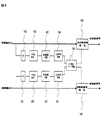
図3はキャンセラ装置の構成を示すブロック図、図4はスロット構成回路による受信信号のスロット構成信号への変換につてい説明する図、図5はスロット構成信号の干渉キャンセルステージの処理過程における信号配置方法について説明する図、図6はステージ処理回路の構成と、該回路での逆拡散信号の加算処理について説明する図、図7は干渉キャンセラ装置の相関回路の構成を説明するブロック図、図8は干渉キャンセラ装置のパス検出回路の構成を説明するブロック図である。図3、図6〜図8において、101は同期処理・初期パス検出回路、102、113、114、404は遅延回路、103はスロット信号構成回路、104、107、109、401、403、405、504、601はセレクタ、105は相関回路、106はパス検出回路、108は符号生成回路、110は再拡散回路、111は合成回路、112は減算処理回路、115はステージ処理回路、116は復調回路、402は加算器、501はシフトレジスタ、502は逆拡散符号設定素子、503は加算回路、505は制御部、506はマッチドフィルタ、602は平均化回路、603は累積加算処理回路、604は忘却平均処理回路、605は逆拡散信号検出回路、606はパス検出・ピーク検出回路である。
【0029】
無線基地局装置12に設けられる干渉キャンセラ装置は、図3に示すように、無線受信部で受信された多重波信号の同期処理と初期のパス位置検出とを行う同期処理・初期パス検出回路101と、パス検出結果を信号の分割に反映させるための遅延を行う遅延回路102と、パス検出を行った受信信号をある時間間隔で分割してスロット構成の信号への変換を行うスロット構成回路103と、スロット信号の信号選択を行うセレクタ104と、スロット構成の信号の逆拡散処理を行う相関回路105と、干渉抑圧信号のパス検出を行うパス検出回路106と、逆拡散処理後の逆拡散信号をステージ処理段数加算を行うステージ加算回路115と、ステージ加算後の信号の再拡散処理を行う再拡散回路110と、再拡散処理を行った全ての信号の合成処理を行いレプリカ信号を生成する合成回路111と、合成処理後のレプリカ信号を受信信号から減算する処理を行う減算処理回路112と、逆拡散、再拡散処理を行う符号を生成する符号生成回路108と、その符号の切り替えを行うセレクタ107、109と、干渉キャンセル後の信号について復調処理を行う復調回路116とにより構成されている。
【0030】
前述において、入力される受信信号は、無線部22により受信された多重波信号を同期処理とパス検出とを行った後の受信信号であり、この受信信号は、スロット信号構成回路103によりある時間間隔で分割され、より高速な周期の信号へと変換した後シリアル的なスロット構成の信号にされる。スロット構成にされた信号は、分割した信号と同じ信号が繰り返し配置されるような構成となっている。このスロット構成にされた信号は、一方は減算処理を行うため繰り返し信号が配置されたスロット構成のまま遅延回路113を介して減算処理部112へ入力される。そして、もう一方のスロット構成の信号は、セレクタ104により、最初の第1スロットの信号のみが通過させられ残りのスロットの信号が遮断された信号に変換された後、干渉キャンセル処理を行うための後段の処理回路へ入力される。
【0031】
第1スロットのみが通過した信号は、逆拡散処理を行うため相関回路105に入力される。この相関回路105は、多重化された入力信号に対して、ユーザー数分の相関検出処理を行い、ユーザー数分の逆拡散処理を行う。逆拡散された信号は、パス検出回路106、ステージ処理回路115を経て、スロット構成のまま再拡散回路110に入力され再拡散信号に作成した後、合成回路111により全てのユーザーの再拡散信号が合成されレプリカ信号に生成される。レプリカ信号は、減算処理回路に入力される繰り返し信号のスロット構成となっている信号と減算処理が行われた後に、逆拡散処理を行う先ほどの相関回路105へ遅延回路114とセレクタ104とを介して帰還される。
【0032】
相関回路105に帰還された減算処理後の信号についても同様に逆拡散処理が行われる。このときの時間的なタイミングは、先ほどの帰還前の信号、つまり受信後の信号が第1スロットの信号であるとすると、この信号を処理して帰還された信号が第2スロットの信号となるように配置され連続して信号の処理を行うことが可能なようにされている。帰還され逆拡散処理された第2スロットの信号についても先ほどの処理と同様に再び再拡散処理、合成処理が行われレプリカ信号が生成される。このレプリカ信号についても、前回同様減算処理を行った後に再び相関回路に帰還されるのである。この帰還された信号は第3スロットの信号となり、同様の処理を繰り返し行うことにより、マルチステージ型の干渉キャンセル機能を持ち、干渉成分の抑圧効果を高めることができる。
【0033】
前述で説明したように、本発明の実施形態は、マルチステージ干渉キャンセラの処理において、受信信号をある時間間隔で分割し、より高速な周期の信号へと変換した後シリアル的なスロット構成に変換した信号を使用する。このスロット構成に変換した信号は相関回路にて逆拡散処理が行われる。このとき、連続信号をスロットに分割することにより不連続信号となるため、そのまま分割した信号をスロットに配置したのでは、不連続点での相関回路による復調処理ができなくなる。そのため、本発明の実施形態は、不連続点においても相関回路による復調が連続信号と同様に行えるようにするため、分割する信号を分割点において前後の分割した信号と一部分の信号が重複するように分割を行い、その信号をスロット構成の信号として配置するものである。この分割方法により不連続点での信号も信号の欠落なく逆拡散処理が可能となる。
【0034】
次に、前述したような信号の分割を行うスロット構成回路103での受信信号をスロット構成の信号に変換する様子を、図4を参照して説明する。
【0035】
受信された信号は、多数の無線移動局装置11の加入者からの信号が符号分割多重された状態の信号であり、スロット構成回路103は、このような受信信号201を任意に設定されたある時間間隔で分割し、より高速な周期の信号へと変換した後シリアルなスロット構成の信号に変換する。この信号変換は、前述の時間間隔で分割した信号を、前述と同一の時間間隔の中にm個の高速な同一の信号として並べて、スロット構成の信号202となるように行われる。
【0036】
受信信号201は、任意に設定されたある時間間隔で分割されるので、無線移動局装置11からの各加入者の信号は、不連続な信号となってしまうため、変換されたスロット信号202は、以後の処理において、不連続点での相関回路による逆拡散処理ができないものとなる。そこで、本発明の実施形態によるここでの信号変換は、不連続点においても相関回路による逆拡散が連続信号と同様に行うことを可能とするため、受信信号201の分割点において、前後の分割した信号と一部分の信号が重複するように分割を行っている。分割された信号は、スロット信号202に示すように分割された信号と同一のものが繰り返してm個配置されるような構成となっている。mは、干渉キャンセル行うステージ処理の段数であり、この段数が多ければ干渉キャンセルの効果が大きくなるがそのための処理時間も多く要することになるので、干渉キャンセルの効果と処理時間とにより、システムとして、最適な値が設定される。
【0037】
本発明の干渉キャンセラの処理は、スロット構成にした信号をスロットの第1スロットに受信信号を配置し逆拡散処理を行い、第2スロットに帰還した信号を配置して逆拡散処理を行うことにより干渉キャンセルステージ処理を行うものである。逆拡散処理後のデータは、スロット毎に逆拡散された逆拡散信号をステージ毎に累積加算を行うことによりステージ処理利得を高める構成とされている。また、この各ステージ処理段での逆拡散信号の累積加算を行う回路は、信号の入出力部にセレクタ回路を設け、加算を行う信号の選択や次段へと送る信号の選択を可能とする構成となっている。多重数が少ない場合等でステージ数が少なくてよい場合、このセレクタを切り替えることによりスロット構成を変えることなくステージ処理段数の変更が可能となる。また、次段へと送る信号をセレクタにより選択することによりレプリカ信号を作成するための復調信号として使用可能な信号の選択が可能となる。
【0038】
次に、前述したような干渉キャンセルステージでの処理過程について図5を参照して説明する。
【0039】
スロット構成回路103によりスロット構成の信号202に変換された信号は2分されて、その一方が、減算処理を行うため前述のスロット構成のまま減算処理部112へ入力され、他の一方が、干渉キャンセルステージ処理を行うため信号301として示すように最初の1スロットの信号のみがセレクタ104により選択されて通過させられて相関回路105に入力される。その後、セレクタ104を通過した信号は、相関回路105による逆拡散処理、再拡散回路110による再拡散処理、合成回路111による合成処理、減算信号回路112による減算処理が行われる。減算処理が行われた信号は、遅延回路114を通り再び相関回路105に帰還される。帰還された信号は、信号302として示すようにスロット構成にした信号の第2、第3スロット、…、へと配置される。
【0040】
帰還された信号は、再び相関回路105により逆拡散処理が行われ、各スロットにおける復調データは、ステージ処理回路115により逆拡散信号の加算処理が行われる。次に、この逆拡散信号の加算処理を図6を参照して説明する。
【0041】
ステージ処理回路115は、図6(a)に示すように、セレクタ401と、加算器402と、セレクタ403と、遅延回路404と、セレクタ405とにより構成されている。入力される逆拡散信号には、加算器402と遅延回路404とにより、前のスロットの逆拡散信号が累積的に加算されていく処理が施される。この結果、ステージ処理回路115から出力される逆拡散信号が累積的に加算された信号は、図6(b)に406として示すようなものとなる。多数の逆拡散信号が累積加算された信号は、干渉がキャンセルされた信号とされていることになり、この信号が復調処理されることにより、干渉がキャンセルされた信号に復調される。
【0042】
相関回路105は、従来、復調するユーザー数と同じ数必要でであったが、本発明の実施形態は、信号処理方法を工夫することにより1つの相関回路で複数のユーザー信号を復調可能となるように構成されている。本発明の実施形態は、この構成によりユーザー数の増加とともに増えていた相関回路の数を減少させることを可能とした。
【0043】
相関回路に入力される受信信号は、シフトレジスタに入力され、順次後段のレジスタにシフトされていく。相関回路は、この受信信号と逆拡散を行う符合を積算し積算結果の和をとることにより相関値を出力し、その処理を連続的に行うことにより信号の復調を行っている。逆拡散を行うために設定される符号は、符号生成回路108により生成され、それぞれのユーザー信号を復調するのに必要な符号をそれぞれ別々に生成する。この生成された逆拡散符号を相関回路の符号設定素子に設定して復調処理を行うのであるが、このときに設定される符号の設定方法が本発明の特徴である。
【0044】
通常、受信信号と逆拡散符号とは、受信信号がオーバーサンプル処理されているためシフトレジスタの遅延段数が異なるが、受信信号と逆拡散符号とは同期するように後段へと送られる。そのため、それぞれの相関回路に入力される受信信号が全く同一であるにもかかわらず設定される逆拡散符合がユーザーにより異なるために復調を行うユーザー数の相関回路が必要となっているのである。そこで、本発明の実施形態は、受信信号がシフトレジスタに設定され後段のレジスタに1つシフトする時間内に、相関回路の符号設定素子に設定される符号を瞬時に切り替えられる構成にし、全てのユーザー信号の逆拡散符号を切り替えて設定を行うことにより複数ユーザー信号の逆拡散処理を可能にしたものである。このとき、設定される符号を切り替える瞬間に同期して復調信号の出力も切り替える構成をとることにより出力には複数ユーザーの相関検出した相関値信号が並列して出力されることになり、1つの相関回路で複数のユーザー信号の逆拡散処理が可能となる。
【0045】
次に、図7を参照して、前述したような相関回路105の構成とその動作とについて説明する。
【0046】
相関回路105は、マッチドフィルタ506として、シフトレジスタ501と、逆拡散符号設定素子502と、加算回路503と、セレクタ504とを備えて構成されている。周知のように、受信信号をベースバンド信号に周波数に変換された信号は、I軸信号とQ軸信号とに分けられているので、マッチドフィルタ506としても、前述の構成を2組備えている。そして、このマッチドフィルタ506には、逆拡散符号を設定するための符号の生成を行う符号生成器108と、セレクタ107と、セレクタの切り替え制御を行う制御部505とが接続されている。
【0047】
符号生成器108は、受信信号の復調を行う全てのユーザーに対する復調用の逆拡散符号の生成を個別に行う。そして、それらの逆拡散符号は、セレクタ107によって順次高速に切り替えられ拡散符号設定素子502に設定される。制御部505は、この逆拡散符号の設定切り替えと同時に相関値の出力を切り替えるセレクタ504の切り替えの制御を行う。セレクタ504の出力には、説明している装置により逆拡散処理可能なユーザー数の信号線が接続されており、セレクタ504の切り替えにより相関回路105の出力には、相関検出した相関値処理が復調ユーザー数分並列に出力される。
【0048】
本発明の実施形態におけるマルチステージ干渉キャンセラ装置で使用するパス検出回路106は、相関検出され干渉キャンセルステージ処理を施した後の信号によりパス検出を行うことを可能としたものである。通常、受信信号の同期処理とパス検出、並びにパス選択は、受信初期に行われ、そのデータに基づいて逆拡散処理が行われる。しかし、符号分割多元接続無線通信システムは、基地局、移動局間で細かな電力制御が行われ、常に受信信号電力と受信干渉電力との比であるSIR が同じとなるように送信電力の制御が行われている。このため、干渉キャンセラにより干渉成分を抑圧された後の信号は、電力を下げるように送信相手側に電力制御信号が送られ、受信信号の電力が除々に小さくなってしまう。このように、干渉キャンセラの干渉抑圧効果により受信信号の電力は徐々に小さくなるため、初段の同期処理、パス検出回路だけでは、パス検出が難しくなってしまう。
【0049】
そこで、本発明の実施形態に使用するパス検出回路106は、受信初期の同期処理、パス検出を通常のパス検出回路にて行うだけでなく、干渉キャンセラにより干渉成分を抑圧した後の信号においてもパス検出を行うことが可能な構成とされている。すなわち、まず、1番最初の第1スロットの信号は、初段のパス検出信号を使用し逆拡散処理を行い、第2スロットの信号は、第1スロットの信号を逆拡散処理したときの相関値信号を使用する。そして、第3スロットの信号を逆拡散処理するときには、第1スロットの相関値信号と、第2スロットの相関値信号との両方を加算した相関値信号を使用する。これは、干渉キャンセル処理を施した干渉キャンセル第1ステージの相関値信号である。同様に、第4スロットの信号を逆拡散処理するときは、第1、第2、第3スロットの相関値信号を加算した干渉キャンセル第2ステージの相関値信号を使用する。同様の処理を続けて行うことにより、干渉キャンセルステージ処理を施した相関値信号を次スロットのパス検出に使用することが可能となる。これら干渉キャンセルステージ処理を施された信号は、干渉キャンセルステージ処理後にメモリされ、後段のデータとの平均化処理が行われることにより、フェージングなどに強くより正確なパス検出を行うことが可能になる。
【0050】
次に、図8を参照して、前述したようなパス検出回路106の構成とその動作とについて説明する。
【0051】
パス検出回路106は、セレクタ601と、平均化回路602と、累積加算回路603と、忘却平均化回路604と、パス検出・ピーク検出回路606と、逆拡散信号検出回路605とから構成されている。この回路においても、I軸信号とQ軸信号とに対応する前述の構成をパス検出・ピーク検出回路606を覗いて2組備えている。パス検出回路106は、相関回路105より出力されている信号線のうち必要な復調信号と、復調信号のうちパス検出に必要なパイロット信号部分とのみをセレクタ601により選択し、1スロット内のパイロット信号を平均化回路602に平均化処理を行わせる。
【0052】
スロット毎に平均化されたパイロット信号の相関値信号は、加算回路によりステージ処理が施された後段の各スロットの平均化された相関値信号と累積加算回路603により累積加算され、干渉キャンセルステージ処理が施された相関値信号とされることになる。この干渉キャンセルステージ処理が行われた相関値信号は、忘却平均回路604により干渉キャンセルステージ処理が施されたいくつかの相関値信号の平均化処理が行われる。この干渉キャンセルステージ処理が施された相関値信号を使用して受信信号のパス検出と、シンボル復調を行うパスのピーク検出とが、パス検出・ピーク検出回路606により行われる。このパス検出・ピーク検出回路606によりピーク検出が行われたパス情報に基づいて、相関回路105より出力される相関値データからシンボル復調データの抽出が行われる。
【0053】
前述した本発明の実施形態によれば、干渉キャンセルステージ処理を施した信号を帰還させて信号の処理を行うことにより、従来の従属接続していたステージ処理と同様の信号処理を可能にした上で、従来ステージ段数必要としていたハード量を大幅に削減することができるという効果を得ることができる。
【0054】
また、前述の本発明の実施形態によれば、復調すべきユーザーの数だけ必要としていた相関回路を高速な逆拡散符号の切り替えと出力の同期切り替えとを行うことにより、1つの相関回路より複数のユーザー信号の復調を行うことを可能にし、これにより、相関回路の数を減少させることができるという効果を得ることができる。
【0055】
さらに、前述した本発明実施形態によれば、干渉キャンセル処理により復調信号の干渉量が減少し、この電力制御に伴い受信電力が小さくなった場合においても受信信号のパス検出を可能にし更に多くの受信信号の多重化が可能になるという効果を得ることができる。
【0056】
【発明の効果】
以上説明したように本発明によれば、複数の無線移動局装置と同時通信を行っている無線基地局装置における、通信ユーザー数の増加により生じる相互相関干渉の抑制を行う干渉抑圧機能を備えることによる装置規模の増大を抑え、チャネルの使用効率の低下を防ぎ、高品質の通信を行うことを可能にした低コストの符号分割多元接続を用いる通信システムを得ることができる。
【図面の簡単な説明】
【図1】本発明の一実施形態による符号分割多元接続を用いる通信システムの構成を示すブロック図である。
【図2】干渉キャンセラ装置を有する無線基地局装置の構成を示すブロック図である。
【図3】干渉キャンセラ装置の構成を示すブロック図である。
【図4】スロット構成回路による受信信号のスロット構成信号への変換につてい説明する図である。
【図5】スロット構成信号の干渉キャンセルステージの処理過程における信号配置方法について説明する図である。
【図6】ステージ処理回路の構成と、該回路での逆拡散信号の加算処理について説明する図である。
【図7】干渉キャンセラ装置の相関回路の構成を説明するブロック図である。
【図8】干渉キャンセラ装置のパス検出回路の構成を説明するブロック図である。
【符号の説明】
11 無線移動局装置(MS)
12 無線基地局装置(BTS)
13 無線説明部(BSC)
14 交換制御部(MSC)
15 公衆通信網
20 アンテナ部
21 送受信増幅部
22 無線部
23 ベースバンド処理部
24 有線伝送路インタフェース部
25 無線基地局制御部
101 同期処理・初期パス検出回路
102、113、114、404 遅延回路
103 スロット信号構成回路
104、107、109、401、403、405、504、601 セレクタ
105 相関回路
106 パス検出回路
108 符号生成回路
110 再拡散回路
111 合成回路
112 減算処理回路
115 ステージ処理回路
116 復調回路
402 加算器
501 シフトレジスタ
502 逆拡散符号設定素子
503 加算回路
505 制御部
506 マッチドフィルタ
602 平均化回路
603 累積加算処理回路
604 忘却平均処理回路
605 逆拡散信号検出回路
606 パス検出・ピーク検出回路[0001]
BACKGROUND OF THE INVENTION
The present invention relates to a communication system, and more particularly, to a radio communication system using a code division multiple access scheme.
[0002]
[Prior art]
A wireless communication system using a code division multiple access scheme has characteristics suitable for mobile communication such as resistance to mutual interference from other systems, resistance to multipath, easy handoff, and excellent secrecy. . However, unlike other multiple access systems, a code division multiple access communication system allows multiple terminal users in the same base station cell to communicate simultaneously using the same frequency and the same frequency band. Therefore, there is a problem with the efficiency of channel use. This problem is caused by interference caused by the user's strong communication signal close to the base station in the presence of near / far problems covering other weak communication signals, interference to other stations caused by unnecessary transmission power from the own station, etc. This is because the channel usage efficiency is reduced.
[0003]
As measures to prevent a decrease in channel use efficiency, use of a wideband gain by widening a signal, use of a code sequence having a small cross-correlation, adoption of power control for solving a near-far problem, and the like are performed. In particular, power control not only suppresses unnecessary transmission power from the own station and minimizes the transmission power of the own station to minimize interference to other stations, but also to solve the near-far problem. Also effective.
[0004]
However, even if these measures are used, it is difficult to prevent a decrease in communication quality due to an increase in cross-correlation interference (deterioration in signal-to-noise ratio) due to an increase in the number of users performing simultaneous communication.
[0005]
As a means for solving the above-described problems, an interference cancellation technique for removing interference from other channels is effective, and various types of interference cancellation techniques are being studied. Interference from other users can be predicted at the receiver, and processing to remove the interference can be performed. Among these interference cancellation methods, an interference cancellation method of a multi-user reception method using a plurality of user signal information to be demodulated has been proposed. An interference cancellation device using this method demodulates a plurality of user signals to be demodulated, performs a respreading process and a synthesizing process from the demodulated signal, creates a replica signal, and receives multiple waves The interference component is suppressed by performing a subtraction process on the signal and a demodulation process. The interference canceling process is performed as a cascaded multi-stage configuration, thereby enhancing the interference component suppression effect.
[0006]
As information on this type of interference cancellation, for example, techniques described in Japanese Patent Application Laid-Open Nos. 10-51353 and 10-190494 are known.
[0007]
[Problems to be solved by the invention]
In a mobile communication system using code division multiple access as described above, an increase in cross-correlation interference due to an increase in the number of users who are simultaneously communicating is inevitable, and an interference cancellation technique is an essential technique. Among these interference cancellation methods, the interference cancellation method of the multi-user reception method uses a plurality of user signal information to be demodulated, and therefore performs interference component suppression processing including multiple correlators and re-spreaders. Requires a signal processor to perform. Since the signal processing unit that performs the interference component suppression processing has a multi-stage configuration in order to enhance the interference component canceling effect, the apparatus scale and the signal processing scale are increased. For this reason, the communication system using such an interference cancellation method has a problem that the scale of the base station apparatus becomes large and the cost also increases.
[0008]
An object of the present invention is to solve the above-described problems of the prior art and suppress cross-correlation interference caused by an increase in the number of communication users in a radio base station apparatus that performs simultaneous communication with a plurality of radio mobile station apparatuses. An object of the present invention is to provide a communication system using code division multiple access that suppresses an increase in apparatus scale due to an interference suppression function.
[0009]
It is another object of the present invention to provide a communication system using low-cost code division multiple access that prevents deterioration in channel use efficiency and enables high-quality communication.
[0010]
[Means for Solving the Problems]
According to the present invention, the object is to provide communication by code division multiple access between a radio base station and a radio mobile station apparatus, comprising a radio base station having an interference canceller apparatus for received signals and a number of radio mobile station apparatuses. In the communication system, the interference canceller divides the received signal at a certain time interval, converts the divided signal into a signal with a higher cycle, and then converts the same signal of the converted signal with a higher cycle A slot configuration circuit for converting a plurality of stages corresponding to the number of stage processing stages into a serial slot configuration signal, a correlation circuit for despreading the slot configuration signal, and stage processing the despread signal after the despread processing A stage addition circuit that adds the number of stages, a respreading circuit that performs respreading of the signal after stage addition, and a replica signal that combines all spread signals that have undergone respreading processing And a subtraction processing circuit that performs subtraction processing between the replica signal and the received signal, and the interference component is obtained by repeatedly feeding back the signal that has been subjected to subtraction processing between the replica signal and the received signal to the correlation circuit. This is achieved by being configured to perform the removal.
[0011]
In addition, the purpose of the slot configuration circuit is to divide a received signal at a certain time interval by dividing so that a part of the preceding and succeeding signals overlap at a signal dividing point. Among the signals of the slot configuration, the slot signal to which the despreading process is performed is a signal in which only the first slot is allowed to pass before being input to the correlation circuit, and the remaining slot signal is not allowed to pass, This is achieved by placing a signal that has been subjected to interference cancellation processing and fed back to the second and subsequent slots at the input of the correlation circuit.
[0012]
Further, the object is that the stage addition circuit performs selection of a valid signal among the input despread signals, selection of a signal for addition, and selection of a signal for respreading. This is achieved by the fact that the number of stage stages can be changed by selecting a despread signal to be added by controlling the selection.
[0013]
Further, the object is that the correlation circuit includes a matched filter having a shift register, a despread code setting element, and an adder circuit, and the matched filter sequentially shifts a received signal input to the shift register to the subsequent stage. In the meantime, when performing a correlation detection process for outputting a correlation value signal by performing an integration process with the despread code setting element and adding the signals after integration, the shift register signal is shifted to the next stage by one stage. This is achieved by performing despreading processing for a plurality of users by switching the despreading codes set in the despreading code setting element within the time and performing correlation detection.
[0014]
Furthermore, the purpose is A path detection circuit for detecting a path of the interference suppression signal; The path detection circuit includes a selector that selects a leading pilot signal portion of the correlation value signal output from the correlation circuit, an averaging circuit that averages the selected pilot signal in the slot signal, and an averaged pilot signal A cumulative addition circuit that performs cumulative addition with the slot signal at the subsequent stage, a signal that has undergone cumulative addition with the other cumulative addition signal after the cumulative addition, a forgetting averaging circuit that performs forgetting averaging processing, and a correlation value that has undergone forgetting averaging A path detection / peak detection circuit that detects the path of the received signal from the signal and performs peak detection and position detection of the effective path, and a despread signal from the correlation value signal based on the effective path information detected by the path detection / peak detection circuit This is achieved by including a despread signal detection circuit that detects the above.
[0015]
DETAILED DESCRIPTION OF THE INVENTION
Embodiments of a communication system according to the present invention will be described below in detail with reference to the drawings.
[0016]
FIG. 1 is a block diagram showing a configuration of a communication system using code division multiple access according to an embodiment of the present invention, and FIG. 2 is a block diagram showing a configuration of a radio base station apparatus having an interference canceller apparatus. An outline of a configuration of the communication system and the radio base station according to the embodiment will be described. 1 and 2, 11 is a radio mobile station device (MS), 12 is a radio base station device (BTS), 13 is a radio control unit (BSC), 14 is an exchange control unit (MSC), and 15 is a public communication network. , 20 is an antenna unit, 21 is a transmission / reception amplification unit, 22 is a radio unit, 23 is a baseband processing unit, 24 is a wired transmission path interface unit, and 25 is a radio base station control unit.
[0017]
As shown in FIG. 1, a mobile communication system to which the present invention is applied includes a radio mobile station apparatus 11, a radio
[0018]
The radio
[0019]
The radio control unit 13 is connected to a plurality of radio
[0020]
As shown in FIG. 2, the radio
[0021]
The
[0022]
The transmission /
[0023]
The radio unit 22 performs D / A conversion on the transmission signal on which baseband signal processing has been performed, converts it into a radio frequency signal after orthogonal modulation, and sends it to a transmission amplifier of the transmission /
[0024]
The baseband
[0025]
The wired transmission
[0026]
The radio base station control unit 25 transmits and receives control signals to and from the radio control unit 13, and performs radio channel management, radio channel setting release, and the like.
[0027]
Next, the detailed configuration and operation of the interference canceller in the radio
[0028]
3 is a block diagram showing the configuration of the canceller apparatus, FIG. 4 is a diagram for explaining the conversion of the received signal into the slot configuration signal by the slot configuration circuit, and FIG. 5 is a signal in the process of the interference cancellation stage of the slot configuration signal. FIG. 6 is a diagram for explaining the arrangement method, FIG. 6 is a diagram for explaining the configuration of the stage processing circuit and despread signal addition processing in the circuit, and FIG. 7 is a block diagram for explaining the configuration of the correlation circuit of the interference canceller apparatus. 8 is a block diagram illustrating a configuration of a path detection circuit of the interference canceller apparatus. 3, FIG. 6 to FIG. 8, 101 is a synchronization processing / initial path detection circuit, 102, 113, 114, 404 are delay circuits, 103 is a slot signal configuration circuit, 104, 107, 109, 401, 403, 405, 504 and 601 are selectors, 105 is a correlation circuit, 106 is a path detection circuit, 108 is a code generation circuit, 110 is a respreading circuit, 111 is a synthesis circuit, 112 is a subtraction processing circuit, 115 is a stage processing circuit, and 116 is a demodulation circuit , 402 is an adder, 501 is a shift register, 502 is a despread code setting element, 503 is an adder circuit, 505 is a control unit, 506 is a matched filter, 602 is an averaging circuit, 603 is a cumulative addition processing circuit, and 604 is forgetting. An average processing circuit, 605 is a despread signal detection circuit, and 606 is a path detection / peak detection circuit.
[0029]
As shown in FIG. 3, the interference canceller apparatus provided in the radio
[0030]
In the above description, the input received signal is a received signal after the multi-wave signal received by the radio unit 22 is subjected to synchronization processing and path detection. This received signal is received by the slot
[0031]
The signal that has passed through only the first slot is input to the
[0032]
The despreading process is similarly performed on the signal after the subtraction process fed back to the
[0033]
As described above, according to the embodiment of the present invention, in the processing of the multistage interference canceller, the received signal is divided at a certain time interval, converted into a signal having a higher period, and then converted into a serial slot configuration. Use the selected signal. The signal converted into the slot configuration is subjected to despreading processing in the correlation circuit. At this time, since the continuous signal is divided into slots and becomes a discontinuous signal, if the divided signal is arranged in the slot as it is, the demodulation processing by the correlation circuit at the discontinuous point cannot be performed. For this reason, in the embodiment of the present invention, in order to enable demodulation by the correlation circuit even at discontinuous points in the same manner as a continuous signal, a signal to be divided is overlapped with a part of the signal divided before and after the division point. And the signal is arranged as a slot-structured signal. With this division method, the signal at the discontinuous point can be despread without loss of signal.
[0034]
Next, how the received signal in the
[0035]
The received signal is a signal in which signals from a number of subscribers of the wireless mobile station apparatus 11 are code-division multiplexed, and the
[0036]
Since the received
[0037]
The processing of the interference canceller of the present invention is performed by despreading a signal having a slot configuration by placing a received signal in the first slot of the slot and performing a despreading process by placing a signal fed back to the second slot. Interference cancellation stage processing is performed. The data after the despreading process is configured to increase the stage processing gain by performing cumulative addition of the despread signal despread for each slot for each stage. In addition, the circuit that performs cumulative addition of the despread signals in each stage processing stage is provided with a selector circuit in the signal input / output unit, so that selection of a signal to be added and selection of a signal to be sent to the next stage are possible. It has a configuration. When the number of stages is small, such as when the number of multiplexing is small, the stage processing stage number can be changed without changing the slot configuration by switching the selector. Further, by selecting a signal to be sent to the next stage with a selector, it is possible to select a signal that can be used as a demodulated signal for creating a replica signal.
[0038]
Next, a process in the interference cancellation stage as described above will be described with reference to FIG.
[0039]
The signal converted into the
[0040]
The feedback signal is despread again by the
[0041]
As shown in FIG. 6A, the
[0042]
Conventionally, the number of
[0043]
The received signal input to the correlation circuit is input to the shift register and sequentially shifted to the subsequent register. The correlation circuit integrates the received signal and the code for despreading and takes the sum of the integration results to output a correlation value, and continuously performs the processing to demodulate the signal. Codes set for despreading are generated by the
[0044]
Normally, the received signal and the despread code have different number of delay stages in the shift register because the received signal is oversampled, but the received signal and the despread code are sent to the subsequent stage so as to be synchronized. For this reason, since the despread code set differs depending on the user even though the received signals inputted to the respective correlation circuits are exactly the same, a correlation circuit for the number of users for performing demodulation is necessary. Therefore, the embodiment of the present invention has a configuration in which the code set in the code setting element of the correlation circuit can be instantaneously switched within the time when the received signal is set in the shift register and shifted by one to the subsequent register. The despreading process of a plurality of user signals is made possible by switching and setting the despread codes of the user signals. At this time, by adopting a configuration in which the output of the demodulated signal is also switched in synchronization with the moment of switching the set code, the correlation value signals detected by the correlation of a plurality of users are output in parallel. The correlation circuit can despread a plurality of user signals.
[0045]
Next, the configuration and operation of the
[0046]
The
[0047]
The
[0048]
The
[0049]
Therefore, the
[0050]
Next, the configuration and operation of the
[0051]
The
[0052]
The correlation value signal of the pilot signal averaged for each slot is subjected to stage processing by the addition circuit, and is cumulatively added by the averaged correlation value signal of each subsequent slot and the
[0053]
According to the above-described embodiment of the present invention, the signal processed by the interference cancellation stage process is fed back to perform the signal processing, thereby enabling the same signal processing as that of the conventional cascade connection stage processing. Thus, it is possible to obtain the effect that the amount of hardware that has conventionally been required for the number of stages can be greatly reduced.
[0054]
Further, according to the above-described embodiment of the present invention, a plurality of correlation circuits required for the number of users to be demodulated are switched from one correlation circuit by switching high-speed despreading codes and switching outputs synchronously. The user signal can be demodulated, and the number of correlation circuits can be reduced.
[0055]
Furthermore, according to the above-described embodiment of the present invention, the amount of interference of the demodulated signal is reduced by the interference cancellation process, and even when the received power is reduced due to this power control, the received signal path can be detected, and more It is possible to obtain an effect that reception signals can be multiplexed.
[0056]
【The invention's effect】
As described above, according to the present invention, the radio base station apparatus that performs simultaneous communication with a plurality of radio mobile station apparatuses has an interference suppression function that suppresses cross-correlation interference caused by an increase in the number of communication users. Thus, it is possible to obtain a communication system using low-cost code division multiple access that suppresses an increase in apparatus scale due to the above, prevents a decrease in channel use efficiency, and enables high-quality communication.
[Brief description of the drawings]
FIG. 1 is a block diagram showing a configuration of a communication system using code division multiple access according to an embodiment of the present invention.
FIG. 2 is a block diagram showing a configuration of a radio base station apparatus having an interference canceller apparatus.
FIG. 3 is a block diagram showing a configuration of an interference canceller apparatus.
FIG. 4 is a diagram for explaining conversion of a received signal into a slot configuration signal by a slot configuration circuit.
FIG. 5 is a diagram illustrating a signal arrangement method in the process of an interference cancellation stage for slot configuration signals.
FIG. 6 is a diagram for explaining the configuration of a stage processing circuit and despread signal addition processing in the circuit.
FIG. 7 is a block diagram illustrating a configuration of a correlation circuit of the interference canceller apparatus.
FIG. 8 is a block diagram illustrating a configuration of a path detection circuit of the interference canceller apparatus.
[Explanation of symbols]
11 Wireless mobile station equipment (MS)
12 Radio base station equipment (BTS)
13 Wireless explanation part (BSC)
14 Exchange Control Unit (MSC)
15 Public communication network
20 Antenna section
21 Transmission / reception amplifier
22 Radio section
23 Baseband processing unit
24 Wired transmission line interface
25 Radio base station controller
101 Synchronization processing and initial path detection circuit
102, 113, 114, 404 delay circuit
103 Slot Signal Configuration Circuit
104, 107, 109, 401, 403, 405, 504, 601 selector
105 Correlation circuit
106 Path detection circuit
108 Code generation circuit
110 Re-diffusion circuit
111 Synthesis circuit
112 Subtraction processing circuit
115 Stage processing circuit
116 Demodulator circuit
402 Adder
501 Shift register
502 Despreading code setting element
503 Adder circuit
505 Control unit
506 matched filter
602 Averaging circuit
603 Cumulative addition processing circuit
604 Forgetting average processing circuit
605 Despread signal detection circuit
606 Path detection / peak detection circuit
Claims (6)
Priority Applications (2)
| Application Number | Priority Date | Filing Date | Title |
|---|---|---|---|
| JP2000020657A JP3686809B2 (en) | 2000-01-28 | 2000-01-28 | Communications system |
| US09/770,819 US6895038B2 (en) | 2000-01-28 | 2001-01-26 | Communication system |
Applications Claiming Priority (1)
| Application Number | Priority Date | Filing Date | Title |
|---|---|---|---|
| JP2000020657A JP3686809B2 (en) | 2000-01-28 | 2000-01-28 | Communications system |
Publications (2)
| Publication Number | Publication Date |
|---|---|
| JP2001217814A JP2001217814A (en) | 2001-08-10 |
| JP3686809B2 true JP3686809B2 (en) | 2005-08-24 |
Family
ID=18547184
Family Applications (1)
| Application Number | Title | Priority Date | Filing Date |
|---|---|---|---|
| JP2000020657A Expired - Fee Related JP3686809B2 (en) | 2000-01-28 | 2000-01-28 | Communications system |
Country Status (2)
| Country | Link |
|---|---|
| US (1) | US6895038B2 (en) |
| JP (1) | JP3686809B2 (en) |
Families Citing this family (9)
| Publication number | Priority date | Publication date | Assignee | Title |
|---|---|---|---|---|
| JP2001320342A (en) * | 2000-05-11 | 2001-11-16 | Nec Corp | Fdm-cdma transmitting method, fdm-cdma receiving method and device for these |
| US20020131534A1 (en) * | 2001-02-07 | 2002-09-19 | Masayuki Ariyoshi | System and method for multistage interference cancellation |
| JP2005130283A (en) * | 2003-10-24 | 2005-05-19 | Matsushita Electric Ind Co Ltd | Matched filter circuit and correlation calculation method |
| JP4297780B2 (en) * | 2003-12-22 | 2009-07-15 | 株式会社ルネサステクノロジ | Receiver |
| US20090149221A1 (en) * | 2004-09-08 | 2009-06-11 | Utstarcom Telecom Co., Ltd. | Centralized base station system based on advanced telecommunication computer architecture platform |
| JP2007274336A (en) * | 2006-03-31 | 2007-10-18 | Fujitsu Ltd | Radio base station and radio terminal |
| EP2247017A1 (en) * | 2008-02-21 | 2010-11-03 | Sharp Kabushiki Kaisha | Transmission device, reception device, communication system, and communication method |
| KR101298589B1 (en) | 2009-09-18 | 2013-08-26 | 부산대학교 산학협력단 | Apparatus and method of feedback cancellation for radio signal |
| CN102918815B (en) * | 2011-05-30 | 2016-03-30 | 华为技术有限公司 | Advanced telecom computing architecture data exchange system and power board, method for interchanging data |
Family Cites Families (6)
| Publication number | Priority date | Publication date | Assignee | Title |
|---|---|---|---|---|
| JP2927657B2 (en) * | 1993-11-05 | 1999-07-28 | ケイディディ株式会社 | Spread spectrum signal demodulator |
| JP3202125B2 (en) * | 1994-03-10 | 2001-08-27 | 沖電気工業株式会社 | Code division multiple access system |
| JPH08206935A (en) | 1995-02-07 | 1996-08-13 | Toshiba Mach Co Ltd | Bed of machine tool |
| KR100212306B1 (en) * | 1995-06-13 | 1999-08-02 | 다치카와 게이지 | Cdma demodulating apparatus |
| JP3390900B2 (en) * | 1996-12-20 | 2003-03-31 | 富士通株式会社 | Interference canceller and provisional determination method |
| US6574270B1 (en) * | 1999-07-30 | 2003-06-03 | Ericsson Inc. | Baseband interference canceling spread spectrum communications methods and apparatus |
-
2000
- 2000-01-28 JP JP2000020657A patent/JP3686809B2/en not_active Expired - Fee Related
-
2001
- 2001-01-26 US US09/770,819 patent/US6895038B2/en not_active Expired - Fee Related
Also Published As
| Publication number | Publication date |
|---|---|
| US20010038664A1 (en) | 2001-11-08 |
| JP2001217814A (en) | 2001-08-10 |
| US6895038B2 (en) | 2005-05-17 |
Similar Documents
| Publication | Publication Date | Title |
|---|---|---|
| US9490857B2 (en) | Systems and methods for parallel signal cancellation | |
| JP5175324B2 (en) | Interference cancellation in spread spectrum communication systems. | |
| EP1021882B1 (en) | Device and method for cancelling code interference in a cdma communication system | |
| US7916699B2 (en) | CDMA communication system and method | |
| CA2552443C (en) | Multichannel cdma subtractive interference canceler | |
| JP2914445B2 (en) | CDMA adaptive receiver | |
| JP4316761B2 (en) | Mobile communication system and radio base station apparatus | |
| WO1994010766A1 (en) | Code division multiplex access mobile communication system | |
| JP4769366B2 (en) | Receiver for a CDMA mobile radio communication system | |
| JP3686809B2 (en) | Communications system | |
| JP2001326971A (en) | Radio base station and mobile communication system | |
| JP3373457B2 (en) | Wireless receiving apparatus and wireless receiving method | |
| KR20000006026A (en) | Line estimation apparatus and communication terminal apparatus | |
| WO2001026243A1 (en) | Cdma receiver, and reception method | |
| JP2013509740A (en) | Method for canceling interference of synchronization channel (SCH) in mobile communication system | |
| JP3650305B2 (en) | Mobile communication system and radio base station apparatus | |
| JP3153531B2 (en) | Direct spread receiver | |
| JP2749237B2 (en) | Mobile communication base station transmitting apparatus and mobile communication system | |
| JP4065320B2 (en) | Method and apparatus for signal acquisition and channel estimation utilizing multiple antennas | |
| JP3600142B2 (en) | Pattern determining method, pattern determining device, searcher device, and communication terminal | |
| JP2930585B1 (en) | Signal receiving apparatus in DS-CDMA system | |
| JP2002044055A (en) | Wireless mobile station and wireless communication system | |
| JP3153530B2 (en) | Direct spread receiver | |
| JP3147112B2 (en) | Direct spread receiver | |
| JPH06152487A (en) | Radio communication system |
Legal Events
| Date | Code | Title | Description |
|---|---|---|---|
| A711 | Notification of change in applicant |
Free format text: JAPANESE INTERMEDIATE CODE: A712 Effective date: 20040727 |
|
| A977 | Report on retrieval |
Free format text: JAPANESE INTERMEDIATE CODE: A971007 Effective date: 20050201 |
|
| A131 | Notification of reasons for refusal |
Free format text: JAPANESE INTERMEDIATE CODE: A131 Effective date: 20050308 |
|
| A521 | Written amendment |
Free format text: JAPANESE INTERMEDIATE CODE: A523 Effective date: 20050426 |
|
| TRDD | Decision of grant or rejection written | ||
| A01 | Written decision to grant a patent or to grant a registration (utility model) |
Free format text: JAPANESE INTERMEDIATE CODE: A01 Effective date: 20050531 |
|
| A61 | First payment of annual fees (during grant procedure) |
Free format text: JAPANESE INTERMEDIATE CODE: A61 Effective date: 20050606 |
|
| R150 | Certificate of patent or registration of utility model |
Free format text: JAPANESE INTERMEDIATE CODE: R150 |
|
| FPAY | Renewal fee payment (event date is renewal date of database) |
Free format text: PAYMENT UNTIL: 20080610 Year of fee payment: 3 |
|
| FPAY | Renewal fee payment (event date is renewal date of database) |
Free format text: PAYMENT UNTIL: 20090610 Year of fee payment: 4 |
|
| FPAY | Renewal fee payment (event date is renewal date of database) |
Free format text: PAYMENT UNTIL: 20100610 Year of fee payment: 5 |
|
| S111 | Request for change of ownership or part of ownership |
Free format text: JAPANESE INTERMEDIATE CODE: R313115 |
|
| FPAY | Renewal fee payment (event date is renewal date of database) |
Free format text: PAYMENT UNTIL: 20100610 Year of fee payment: 5 |
|
| R350 | Written notification of registration of transfer |
Free format text: JAPANESE INTERMEDIATE CODE: R350 |
|
| FPAY | Renewal fee payment (event date is renewal date of database) |
Free format text: PAYMENT UNTIL: 20100610 Year of fee payment: 5 |
|
| FPAY | Renewal fee payment (event date is renewal date of database) |
Free format text: PAYMENT UNTIL: 20110610 Year of fee payment: 6 |
|
| LAPS | Cancellation because of no payment of annual fees |