JP3672902B2 - Method for protecting the surface of a semiconductor substrate - Google Patents
Method for protecting the surface of a semiconductor substrate Download PDFInfo
- Publication number
- JP3672902B2 JP3672902B2 JP2002298452A JP2002298452A JP3672902B2 JP 3672902 B2 JP3672902 B2 JP 3672902B2 JP 2002298452 A JP2002298452 A JP 2002298452A JP 2002298452 A JP2002298452 A JP 2002298452A JP 3672902 B2 JP3672902 B2 JP 3672902B2
- Authority
- JP
- Japan
- Prior art keywords
- semiconductor substrate
- protecting
- higher fatty
- fatty acid
- linear
- Prior art date
- Legal status (The legal status is an assumption and is not a legal conclusion. Google has not performed a legal analysis and makes no representation as to the accuracy of the status listed.)
- Expired - Fee Related
Links
- 239000004065 semiconductor Substances 0.000 title claims description 73
- 239000000758 substrate Substances 0.000 title claims description 64
- 238000000034 method Methods 0.000 title claims description 34
- 235000014113 dietary fatty acids Nutrition 0.000 claims description 18
- 239000000194 fatty acid Substances 0.000 claims description 18
- 229930195729 fatty acid Natural products 0.000 claims description 18
- 150000004665 fatty acids Chemical class 0.000 claims description 18
- 238000010438 heat treatment Methods 0.000 claims description 15
- 230000003647 oxidation Effects 0.000 claims description 12
- 238000007254 oxidation reaction Methods 0.000 claims description 12
- 238000009835 boiling Methods 0.000 claims description 10
- 238000004140 cleaning Methods 0.000 claims description 10
- 230000015572 biosynthetic process Effects 0.000 claims description 7
- 239000000356 contaminant Substances 0.000 claims description 6
- 238000004528 spin coating Methods 0.000 claims description 2
- 238000000151 deposition Methods 0.000 claims 1
- 230000008021 deposition Effects 0.000 claims 1
- 238000007598 dipping method Methods 0.000 claims 1
- 150000002894 organic compounds Chemical class 0.000 description 31
- 229940126214 compound 3 Drugs 0.000 description 16
- 239000000126 substance Substances 0.000 description 16
- 238000004519 manufacturing process Methods 0.000 description 7
- 239000011248 coating agent Substances 0.000 description 5
- 238000000576 coating method Methods 0.000 description 5
- 230000000694 effects Effects 0.000 description 5
- 238000007796 conventional method Methods 0.000 description 4
- 239000002957 persistent organic pollutant Substances 0.000 description 3
- QGZKDVFQNNGYKY-UHFFFAOYSA-N Ammonia Chemical compound N QGZKDVFQNNGYKY-UHFFFAOYSA-N 0.000 description 2
- KRHYYFGTRYWZRS-UHFFFAOYSA-N Fluorane Chemical compound F KRHYYFGTRYWZRS-UHFFFAOYSA-N 0.000 description 2
- VEXZGXHMUGYJMC-UHFFFAOYSA-N Hydrochloric acid Chemical compound Cl VEXZGXHMUGYJMC-UHFFFAOYSA-N 0.000 description 2
- QAOWNCQODCNURD-UHFFFAOYSA-N Sulfuric acid Chemical compound OS(O)(=O)=O QAOWNCQODCNURD-UHFFFAOYSA-N 0.000 description 2
- 238000011109 contamination Methods 0.000 description 2
- 238000010586 diagram Methods 0.000 description 2
- UKMSUNONTOPOIO-UHFFFAOYSA-N docosanoic acid Chemical compound CCCCCCCCCCCCCCCCCCCCCC(O)=O UKMSUNONTOPOIO-UHFFFAOYSA-N 0.000 description 2
- 238000007654 immersion Methods 0.000 description 2
- 230000010354 integration Effects 0.000 description 2
- 239000000463 material Substances 0.000 description 2
- 125000000896 monocarboxylic acid group Chemical group 0.000 description 2
- 230000001681 protective effect Effects 0.000 description 2
- 239000007921 spray Substances 0.000 description 2
- 238000003860 storage Methods 0.000 description 2
- 235000021357 Behenic acid Nutrition 0.000 description 1
- XUIMIQQOPSSXEZ-UHFFFAOYSA-N Silicon Chemical compound [Si] XUIMIQQOPSSXEZ-UHFFFAOYSA-N 0.000 description 1
- 229910021529 ammonia Inorganic materials 0.000 description 1
- 229940116226 behenic acid Drugs 0.000 description 1
- 150000001875 compounds Chemical class 0.000 description 1
- 150000001923 cyclic compounds Chemical class 0.000 description 1
- 238000007599 discharging Methods 0.000 description 1
- 238000005530 etching Methods 0.000 description 1
- 239000007788 liquid Substances 0.000 description 1
- 238000004518 low pressure chemical vapour deposition Methods 0.000 description 1
- 229910052751 metal Inorganic materials 0.000 description 1
- 239000002184 metal Substances 0.000 description 1
- 150000002739 metals Chemical class 0.000 description 1
- 239000000203 mixture Substances 0.000 description 1
- 239000005416 organic matter Substances 0.000 description 1
- 239000002245 particle Substances 0.000 description 1
- 230000000737 periodic effect Effects 0.000 description 1
- JRKICGRDRMAZLK-UHFFFAOYSA-L peroxydisulfate Chemical compound [O-]S(=O)(=O)OOS([O-])(=O)=O JRKICGRDRMAZLK-UHFFFAOYSA-L 0.000 description 1
- 229910052710 silicon Inorganic materials 0.000 description 1
- 239000010703 silicon Substances 0.000 description 1
- 239000013589 supplement Substances 0.000 description 1
- 230000009466 transformation Effects 0.000 description 1
Images


Classifications
-
- H—ELECTRICITY
- H01—ELECTRIC ELEMENTS
- H01L—SEMICONDUCTOR DEVICES NOT COVERED BY CLASS H10
- H01L21/00—Processes or apparatus adapted for the manufacture or treatment of semiconductor or solid state devices or of parts thereof
- H01L21/02—Manufacture or treatment of semiconductor devices or of parts thereof
- H01L21/02104—Forming layers
- H01L21/02107—Forming insulating materials on a substrate
- H01L21/02296—Forming insulating materials on a substrate characterised by the treatment performed before or after the formation of the layer
- H01L21/02299—Forming insulating materials on a substrate characterised by the treatment performed before or after the formation of the layer pre-treatment
- H01L21/02301—Forming insulating materials on a substrate characterised by the treatment performed before or after the formation of the layer pre-treatment in-situ cleaning
-
- H—ELECTRICITY
- H01—ELECTRIC ELEMENTS
- H01L—SEMICONDUCTOR DEVICES NOT COVERED BY CLASS H10
- H01L21/00—Processes or apparatus adapted for the manufacture or treatment of semiconductor or solid state devices or of parts thereof
- H01L21/02—Manufacture or treatment of semiconductor devices or of parts thereof
- H01L21/02041—Cleaning
- H01L21/02043—Cleaning before device manufacture, i.e. Begin-Of-Line process
- H01L21/02052—Wet cleaning only
-
- H—ELECTRICITY
- H01—ELECTRIC ELEMENTS
- H01L—SEMICONDUCTOR DEVICES NOT COVERED BY CLASS H10
- H01L21/00—Processes or apparatus adapted for the manufacture or treatment of semiconductor or solid state devices or of parts thereof
- H01L21/02—Manufacture or treatment of semiconductor devices or of parts thereof
- H01L21/02104—Forming layers
- H01L21/02107—Forming insulating materials on a substrate
- H01L21/02109—Forming insulating materials on a substrate characterised by the type of layer, e.g. type of material, porous/non-porous, pre-cursors, mixtures or laminates
- H01L21/02112—Forming insulating materials on a substrate characterised by the type of layer, e.g. type of material, porous/non-porous, pre-cursors, mixtures or laminates characterised by the material of the layer
- H01L21/02118—Forming insulating materials on a substrate characterised by the type of layer, e.g. type of material, porous/non-porous, pre-cursors, mixtures or laminates characterised by the material of the layer carbon based polymeric organic or inorganic material, e.g. polyimides, poly cyclobutene or PVC
-
- H—ELECTRICITY
- H01—ELECTRIC ELEMENTS
- H01L—SEMICONDUCTOR DEVICES NOT COVERED BY CLASS H10
- H01L21/00—Processes or apparatus adapted for the manufacture or treatment of semiconductor or solid state devices or of parts thereof
- H01L21/02—Manufacture or treatment of semiconductor devices or of parts thereof
- H01L21/02104—Forming layers
- H01L21/02107—Forming insulating materials on a substrate
- H01L21/02225—Forming insulating materials on a substrate characterised by the process for the formation of the insulating layer
- H01L21/0226—Forming insulating materials on a substrate characterised by the process for the formation of the insulating layer formation by a deposition process
- H01L21/02282—Forming insulating materials on a substrate characterised by the process for the formation of the insulating layer formation by a deposition process liquid deposition, e.g. spin-coating, sol-gel techniques, spray coating
-
- H—ELECTRICITY
- H01—ELECTRIC ELEMENTS
- H01L—SEMICONDUCTOR DEVICES NOT COVERED BY CLASS H10
- H01L21/00—Processes or apparatus adapted for the manufacture or treatment of semiconductor or solid state devices or of parts thereof
- H01L21/02—Manufacture or treatment of semiconductor devices or of parts thereof
- H01L21/04—Manufacture or treatment of semiconductor devices or of parts thereof the devices having at least one potential-jump barrier or surface barrier, e.g. PN junction, depletion layer or carrier concentration layer
- H01L21/18—Manufacture or treatment of semiconductor devices or of parts thereof the devices having at least one potential-jump barrier or surface barrier, e.g. PN junction, depletion layer or carrier concentration layer the devices having semiconductor bodies comprising elements of Group IV of the Periodic System or AIIIBV compounds with or without impurities, e.g. doping materials
- H01L21/30—Treatment of semiconductor bodies using processes or apparatus not provided for in groups H01L21/20 - H01L21/26
- H01L21/31—Treatment of semiconductor bodies using processes or apparatus not provided for in groups H01L21/20 - H01L21/26 to form insulating layers thereon, e.g. for masking or by using photolithographic techniques; After treatment of these layers; Selection of materials for these layers
- H01L21/312—Organic layers, e.g. photoresist
-
- C11D2111/22—
Description
【0001】
【発明の属する技術分野】
本発明は、半導体基板、特にシリコン半導体基板の清浄表面を有機物で汚染されない状態に保持するための半導体基板の表面保護方法に関するものである。
【0002】
【従来の技術】
一般に、従来の半導体基板の洗浄方法は、フッ化水素酸、アンモニア過水、硫酸過水、塩酸過水等の化学薬品を用いて自然酸化膜及び汚染物質を除去し、高清浄な表面状態にしていた。近年、半導体素子の高集積化に伴って、半導体表面をより一層高清浄化し、その状態を保持する必要が生じてきた。
【0003】
すなわち、半導体基板の表面には、製造過程に伴って種々の汚染物質が付着するため、高集積化に対応するためには、製造過程で付着する小径な微粒子、金属、有機物を除去するだけでなく、洗浄後から次の工程までの放置状態にある間の有機物の付着も防ぐことが必要になってきている。
【0004】
この有機物は、一般にクリーンルームの空気中に存在し、その中に放置するだけで簡単にしかも短時間に付着してしまう。一時的にこれを防ぐ方法として、現在、ミニエンバイロメントの手法やケミカルフィルターによる有機物除去の手法が用いられている。
【0005】
【発明が解決しようとする課題】
しかしながら、上記した従来の方法では、以下のような問題点が生じている。ミニエンバイロメントではポット等を使用し基板を密閉状態に保持しなければならず、そのポットの必要性やポット開閉のためのインターフェース等の多大な投資が必要となっている。
【0006】
また、ケミカルフィルターも製造装置・クリーンルーム空気取り入れ口等を設けなければならず、更に定期的な交換も必要であり、こちらも多大な投資が必要である。
【0007】
本発明は、上記状況に鑑みて、多大な投資を要することなく、簡便に、清浄表面を得た後も汚染物質の付着を防止し、その表面保持を行うことができる半導体基板の表面保護方法を提供することを目的とする。
【0008】
【課題を解決するための手段】
本発明は、上記目的を達成するために、
〔1〕半導体基板の表面保護方法において、半導体基板の半導体洗浄中又は半導体洗浄後に、前記半導体基板の表面上に、後ほど処理される酸化・CVD装置での酸化・成膜時の熱処理温度より低い温度の沸点温度を持つ直鎖状高級脂肪酸を付着させ、有機汚染物質の付着を防止し、前記半導体基板の表面保護を行うことを特徴とする。
【0009】
〔2〕上記〔1〕記載の半導体基板の表面保護方法において、前記直鎖状高級脂肪酸を前記半導体基板表面上に均一にコーティングすることを特徴とする。
【0010】
〔3〕上記〔2〕記載の半導体基板の表面保護方法において、前記直鎖状高級脂肪酸を前記半導体基板へ回転塗布により付着させることを特徴とする。
【0011】
〔4〕上記〔2〕記載の半導体基板の表面保護方法において、前記直鎖状高級脂肪酸をこの直鎖状高級脂肪酸を含む槽への前記半導体基板の浸漬により付着させることを特徴とする。
【0012】
〔5〕半導体基板の表面保護方法において、半導体基板の半導体洗浄中又は半導体洗浄後に、前記半導体基板の表面上に酸化・CVD装置での酸化・成膜時の熱処理温度より低い温度の沸点温度を持つ直鎖状高級脂肪酸を付着させ、有機汚染物質による作用を防止し、前記酸化・成膜工程での熱処理温度により前記直鎖状高級脂肪酸を消失させることを特徴とする。
【0013】
【発明の実施の形態】
以下、本発明の実施の形態について詳細に説明する。
【0014】
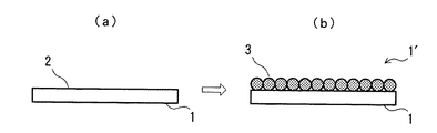
図1は本発明の第1実施例を示す半導体基板の表面保護方法の説明図である。
【0015】
まず、図1(a)に示すように、従来の方法で半導体基板1の洗浄を行い、その半導体基板1の高清浄表面2を生成した直後、もしくは前記洗浄中に、図1(b)に示すように、酸化・CVD装置での酸化・成膜時の熱処理温度より低い温度の沸点温度を持つ直鎖状高級脂肪酸(以下、直鎖状有機化合物)3を高清浄表面2に付着させる。1′はその直鎖状有機化合物3が半導体基板1の高清浄表面2に付着した状態を示している。
【0016】
この直鎖状有機化合物3は常温でウエハを放置しても表面上から揮発しづらい物質であり、通常の熱処理温度より低い沸点の物質を選ぶので、次工程の熱処理で実際に熱処理を行う前に除去できる。ここで、次工程の熱処理とは、一般に熱酸化や減圧CVD等であり、熱温度は熱酸化が700℃〜1100℃、減圧CVD法が500℃〜800℃程度である。
【0017】
表面に付着させる直鎖状有機化合物3は、この熱温度より沸点が低い物質を用いるので、例えば以下に示す有機化合物が挙げられる。ベヘニン酸(C21H43COOH):分子量 340.57,沸点 306℃
以上のように、本発明の第1実施例によれば、図2に示すように、直鎖状有機化合物3を半導体基板1の高清浄表面2上に付着させることにより、一度付着した有機化合物3は表面上から揮発し難く、直鎖状有機汚染物質4と作用して高清浄表面2が汚染されることもない。
【0018】
この有機化合物3〔文献1「半導体プロセス環境における化学汚染とその対策」,リアライズ社、P.268,269〕は、半導体を製造する上で障害となる有機物との置き換わりも起こらない。また、直鎖状有機化合物3は半導体製造工程の熱処理工程の中で、半導体基板の高清浄表面2上から消失するため、半導体基板1が付着させた直鎖状有機化合物3の影響を受けることなく熱処理工程を行うことができる。
【0019】
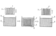
図3は本発明の第2実施例を示す半導体基板の表面保護方法の説明図である。
【0020】
まず、従来の方法で半導体基板1の洗浄を行い、高清浄表面2を製造した直後、もしくは前記清浄中に、直鎖状有機化合物3を高清浄表面2に付着させる。この付着させる方法として、半導体基板1を回転させながらスプレー式ノズル5からの直鎖状有機化合物3を含む液の吐出により基板表面2に直鎖状有機化合物3を付着させる。
【0021】
以上のように、第2実施例によれば、直鎖状有機化合物3を半導体基板表面2に均一に付着させる効果が期待できる。
【0022】
図4は本発明の第3実施例を示す半導体基板の表面保護方法の説明図である。
【0023】
まず、従来の方法で半導体基板1の洗浄を行い、高清浄表面を製造した直後、もしくは前記清浄中に、直鎖状高級脂肪酸(以下、直鎖状有機化合物)3を半導体基板1の表面に付着させる。
【0024】
この付着させる方法として、直鎖状有機化合物3を混入させた槽6の中に半導体基板収納容器7内に縦置きにした半導体基板1を挿入し、半導体基板1表面上に直鎖状有機化合物3を付着させたところで、静かに槽6の中から引き上げる方法である。すなわち、直鎖状有機化合物3を含む溶液浴槽での浸漬による方法である。
【0025】
以上のように、第3実施例によれば、直鎖状有機化合物3を半導体基板1の表面に均一に付着させる効果が期待できる。また、この方法によれば、一度に複数枚の半導体基板1に直鎖状有機化合物3を付着させることができる。直鎖状有機化合物3の組成でCOOH基を含んだものを使用すると、半導体基板1の表面上に、より均一に付着させる効果が期待できる。
【0026】
また、本発明は、直鎖状で、かつ次工程ウエハ処理の熱処理温度よりも低い沸点を有する有機化合物で洗浄されたウエハをコーティングすることを特徴している。
【0027】
(1)直鎖状有機化合物をコーティングしたことにより、コーティング状態が安全に保たれる。すなわち、有機物の吸着は低分子のものが最初に付き、それが高分子のものに置き換わって行くことを利用して、コーティング状態を良好なものにすることができる。つまり、最初から直鎖状有機化合物が表面にコーティングされていると、その他の物質に置き換わる確率が激減することになり、コーティング状態を良好なものにすることができる。
【0028】
(2)エッチング、またはCVD膜形成などのウエハ処理をする際、上記直鎖状有機化合物は、ウエハ上に残さとして残らず、剥離しやすい必要がある。有機物には、直鎖状有機化合物、環状化合物(二重結合なし)、また環状二重結合化合物の大きく3タイプがあり、上記目的を満足し、半導体製造で使用する温度、雰囲気で十分に除去することができるのが、直鎖状有機化合物であり、このタイプを選択した理由である。
【0029】
(3)また、上記(2)の補充として、次工程となるウエハ処理の熱処理温度よりも低い沸点の物質を選ぶことにより、次工程の熱処理で実際に熱処理を行う前に除去できるようになる。
【0030】
なお、本発明は上記実施例に限定されるものではなく、本発明の趣旨に基づいて種々の変形が可能であり、これらを本発明の範囲から排除するものではない。
【0031】
【発明の効果】
以上、詳細に説明したように、本発明によれば、多大な投資を要することなく、簡便に半導体基板の清浄表面を得た後のその表面保持を行うことができる。
【0032】
また、有機汚染物質による作用を防止し、次工程での処理温度により直鎖状高級脂肪酸(直鎖状有機化合物)を消失させることができ、処理工程上では何ら障害をもたらさずに清浄表面を保持することができる。
【図面の簡単な説明】
【図1】 本発明の第1実施例を示す半導体基板の表面保護方法の説明図である。
【図2】 本発明の第1実施例を示す半導体基板の表面保護方法の効果の説明図である。
【図3】 本発明の第2実施例を示す半導体基板の表面保護物塗布の説明図である。
【図4】 本発明の第3実施例を示す半導体基板の表面保護物の浸漬の説明図である。
【符号の説明】
1 半導体基板
1′ 直鎖状有機化合物が塗布された状態の半導体基板
2 半導体基板の高清浄表面
3 直鎖状高級脂肪酸(直鎖状有機化合物)
4 有機汚染物質
5 スプレー式ノズル
6 有機化合物を混入させた槽
7 半導体基板収納容器[0001]
BACKGROUND OF THE INVENTION
The present invention relates to a method for protecting a surface of a semiconductor substrate, in particular, a semiconductor substrate for maintaining a clean surface of a silicon semiconductor substrate in a state not contaminated with organic substances.
[0002]
[Prior art]
In general, conventional semiconductor substrate cleaning methods remove natural oxide films and contaminants using chemicals such as hydrofluoric acid, ammonia perwater, sulfuric acid persulfate, and hydrochloric acid perwater to achieve a highly clean surface condition. It was. In recent years, along with the high integration of semiconductor elements, it has become necessary to further clean the surface of the semiconductor and maintain the state.
[0003]
In other words, various contaminants adhere to the surface of the semiconductor substrate along with the manufacturing process. To cope with high integration, it is only necessary to remove small particles, metals, and organic substances adhering during the manufacturing process. In addition, it has become necessary to prevent the adhesion of organic substances during the standing state from the cleaning to the next step.
[0004]
This organic substance is generally present in the air of a clean room, and simply attaches in a short time just by leaving it in it. Currently, as a method for temporarily preventing this, a mini-environment method and a method for removing organic substances using a chemical filter are used.
[0005]
[Problems to be solved by the invention]
However, the conventional methods described above have the following problems. In the mini-environment, a pot or the like must be used to hold the substrate in a hermetically sealed state, which requires a great investment such as the necessity of the pot and an interface for opening and closing the pot.
[0006]
In addition, the chemical filter must be provided with a manufacturing device, a clean room air intake, and the like, and further periodic replacement is required, which also requires a great investment.
[0007]
In view of the above situation, the present invention is a method for protecting a surface of a semiconductor substrate, which can easily prevent contamination and maintain the surface even after obtaining a clean surface without requiring a large investment. The purpose is to provide.
[0008]
[Means for Solving the Problems]
In order to achieve the above object, the present invention provides
[1] In the method for protecting a surface of a semiconductor substrate, during or after the semiconductor cleaning of the semiconductor substrate, the surface of the semiconductor substrate is lower than the heat treatment temperature during oxidation / film formation in an oxidation / CVD apparatus to be processed later. a linear higher fatty acid having a boiling point temperature of the temperature adhered to prevent adhesion of organic contaminants, and performs surface protection of the semiconductor substrate.
[0009]
[2] The method for protecting a surface of a semiconductor substrate according to [1], wherein the linear higher fatty acid is uniformly coated on the surface of the semiconductor substrate.
[0010]
[3] The method for protecting a surface of a semiconductor substrate according to [2], wherein the linear higher fatty acid is attached to the semiconductor substrate by spin coating.
[0011]
[4] The method for protecting a surface of a semiconductor substrate according to [2] above, wherein the linear higher fatty acid is adhered by immersing the semiconductor substrate in a tank containing the linear higher fatty acid .
[0012]
[5] The surface protecting method of the semiconductor substrate, after the semiconductor cleaning during or semiconductor cleaning of the semiconductor substrate, the boiling point of the heat treatment temperature by Ri low temperature during oxidation and formation of the oxidation-CVD device on the surface of the semiconductor substrate It is characterized in that a linear higher fatty acid having a temperature is attached to prevent the action due to organic pollutants, and the linear higher fatty acid is eliminated by a heat treatment temperature in the oxidation / film formation step.
[0013]
DETAILED DESCRIPTION OF THE INVENTION
Hereinafter, embodiments of the present invention will be described in detail.
[0014]
FIG. 1 is an explanatory view of a method for protecting a surface of a semiconductor substrate according to a first embodiment of the present invention.
[0015]
First, as shown in FIG. 1A, the
[0016]
The linear
[0017]
Since the linear
As described above, according to the first embodiment of the present invention, as shown in FIG. 2, by attaching the linear
[0018]
This organic compound 3 [
[0019]
FIG. 3 is an explanatory diagram of a method for protecting a surface of a semiconductor substrate according to a second embodiment of the present invention.
[0020]
First, the
[0021]
As described above, according to the second embodiment, the effect of uniformly attaching the linear
[0022]
FIG. 4 is an explanatory view of a method for protecting a surface of a semiconductor substrate according to a third embodiment of the present invention.
[0023]
First, the
[0024]
As this adhesion method, the
[0025]
As described above, according to the third embodiment, an effect of uniformly attaching the linear
[0026]
In addition, the present invention is characterized in that a wafer washed with an organic compound that is linear and has a boiling point lower than the heat treatment temperature of the next wafer process is coated.
[0027]
(1) The coating state is kept safe by coating the linear organic compound. That is, the organic matter can be adsorbed with a low molecular weight first, and is replaced with a high molecular weight one, so that the coating state can be improved. That is, when the linear organic compound is coated on the surface from the beginning, the probability of being replaced with another substance is drastically reduced, and the coating state can be improved.
[0028]
(2) When performing wafer processing such as etching or CVD film formation, the linear organic compound does not remain as a residue on the wafer and needs to be easily peeled off. There are three main types of organic substances: linear organic compounds, cyclic compounds (without double bonds), and cyclic double bond compounds, which satisfy the above objectives and are sufficiently removed at temperatures and atmospheres used in semiconductor manufacturing. What can be done is a linear organic compound, which is why this type was chosen.
[0029]
(3) Further, as a supplement to the above (2), by selecting a substance having a boiling point lower than the heat treatment temperature of the next wafer process, it becomes possible to remove the heat treatment in the next process before actually performing the heat treatment. .
[0030]
In addition, this invention is not limited to the said Example, A various deformation | transformation is possible based on the meaning of this invention, and these are not excluded from the scope of the present invention.
[0031]
【The invention's effect】
As described above in detail, according to the present invention, it is possible to easily retain the surface of the semiconductor substrate after obtaining a clean surface without requiring a great investment.
[0032]
In addition, the action of organic pollutants can be prevented, and linear higher fatty acids ( linear organic compounds ) can be eliminated by the processing temperature in the next process, and the clean surface can be removed without causing any obstacles in the processing process. Can be held.
[Brief description of the drawings]
FIG. 1 is an explanatory diagram of a method for protecting a surface of a semiconductor substrate according to a first embodiment of the present invention.
FIG. 2 is an explanatory view of the effect of the semiconductor substrate surface protection method according to the first embodiment of the present invention;
FIG. 3 is an explanatory view of coating a surface protective material on a semiconductor substrate according to a second embodiment of the present invention.
FIG. 4 is an explanatory view of immersion of a surface protective material of a semiconductor substrate according to a third embodiment of the present invention.
[Explanation of symbols]
DESCRIPTION OF
4 Organic pollutant 5
Claims (5)
Priority Applications (3)
| Application Number | Priority Date | Filing Date | Title |
|---|---|---|---|
| JP2002298452A JP3672902B2 (en) | 2002-10-11 | 2002-10-11 | Method for protecting the surface of a semiconductor substrate |
| US10/660,490 US7189657B2 (en) | 2002-10-11 | 2003-09-12 | Semiconductor substrate surface protection method |
| US11/700,889 US7514371B2 (en) | 2002-10-11 | 2007-02-01 | Semiconductor substrate surface protection method |
Applications Claiming Priority (1)
| Application Number | Priority Date | Filing Date | Title |
|---|---|---|---|
| JP2002298452A JP3672902B2 (en) | 2002-10-11 | 2002-10-11 | Method for protecting the surface of a semiconductor substrate |
Publications (2)
| Publication Number | Publication Date |
|---|---|
| JP2004134609A JP2004134609A (en) | 2004-04-30 |
| JP3672902B2 true JP3672902B2 (en) | 2005-07-20 |
Family
ID=32064215
Family Applications (1)
| Application Number | Title | Priority Date | Filing Date |
|---|---|---|---|
| JP2002298452A Expired - Fee Related JP3672902B2 (en) | 2002-10-11 | 2002-10-11 | Method for protecting the surface of a semiconductor substrate |
Country Status (2)
| Country | Link |
|---|---|
| US (2) | US7189657B2 (en) |
| JP (1) | JP3672902B2 (en) |
Families Citing this family (1)
| Publication number | Priority date | Publication date | Assignee | Title |
|---|---|---|---|---|
| US20150017774A1 (en) * | 2013-07-10 | 2015-01-15 | Globalfoundries Inc. | Method of forming fins with recess shapes |
Family Cites Families (9)
| Publication number | Priority date | Publication date | Assignee | Title |
|---|---|---|---|---|
| US4581315A (en) * | 1979-06-25 | 1986-04-08 | University Patents, Inc. | Photoresistive compositions |
| KR0145061B1 (en) | 1990-03-16 | 1998-08-17 | 아오이 죠이치 | Method and apparatus for cleaning |
| EP0560617A3 (en) * | 1992-03-13 | 1993-11-24 | Kawasaki Steel Co | Method of manufacturing insulating film on semiconductor device and apparatus for carrying out the same |
| JP3690619B2 (en) * | 1996-01-12 | 2005-08-31 | 忠弘 大見 | Cleaning method and cleaning device |
| US5827444A (en) * | 1996-03-01 | 1998-10-27 | Taiho Industries Co., Ltd. | Stabilized magnetic fluid and method for stabilizing magnetic fluid |
| US5932493A (en) | 1997-09-15 | 1999-08-03 | International Business Machines Corporaiton | Method to minimize watermarks on silicon substrates |
| US6165956A (en) | 1997-10-21 | 2000-12-26 | Lam Research Corporation | Methods and apparatus for cleaning semiconductor substrates after polishing of copper film |
| JPH11291639A (en) * | 1998-04-10 | 1999-10-26 | Sony Corp | Recording material and method for recording |
| JP2003100865A (en) * | 2001-09-21 | 2003-04-04 | Catalysts & Chem Ind Co Ltd | Semiconductor substrate and method of manufacturing the same |
-
2002
- 2002-10-11 JP JP2002298452A patent/JP3672902B2/en not_active Expired - Fee Related
-
2003
- 2003-09-12 US US10/660,490 patent/US7189657B2/en not_active Expired - Fee Related
-
2007
- 2007-02-01 US US11/700,889 patent/US7514371B2/en not_active Expired - Fee Related
Also Published As
| Publication number | Publication date |
|---|---|
| JP2004134609A (en) | 2004-04-30 |
| US20070134933A1 (en) | 2007-06-14 |
| US7514371B2 (en) | 2009-04-07 |
| US7189657B2 (en) | 2007-03-13 |
| US20040072707A1 (en) | 2004-04-15 |
Similar Documents
| Publication | Publication Date | Title |
|---|---|---|
| US5723019A (en) | Drip chemical delivery method and apparatus | |
| JP3333684B2 (en) | Polishing treatment method | |
| JP2010109384A (en) | Method of removing metal in scrubber | |
| KR100220926B1 (en) | A cleaning method for hydrophobic silicon wafers | |
| WO2006068127A1 (en) | Method for producing epitaxial silicon wafer | |
| JPH09293701A (en) | Manufacture of semiconductor | |
| US6558233B1 (en) | Wafer polishing method, wafer cleaning method and wafer protective film | |
| JP3672902B2 (en) | Method for protecting the surface of a semiconductor substrate | |
| US6354309B1 (en) | Process for treating a semiconductor substrate | |
| JP2003203900A (en) | Wafer-processing device and wafer-processing method | |
| CN114496710A (en) | Method for cleaning yttrium oxide coating of ceramic window of semiconductor equipment | |
| US20020179112A1 (en) | Method of cleaning electronic device | |
| JP3036366B2 (en) | Processing method of semiconductor silicon wafer | |
| JP3595681B2 (en) | Manufacturing method of epitaxial wafer | |
| JP3353477B2 (en) | Pure water rinsing method and semiconductor device manufacturing method | |
| JPH056884A (en) | Cleaning method for silicon wafer | |
| KR102648258B1 (en) | Glass carrier cleaning using ozone | |
| JP2002176025A (en) | Semiconductor substrate cleaning device and method of cleaning semiconductor substrate using it | |
| JP3657867B2 (en) | Liquid material application apparatus and liquid material application method | |
| JP4306217B2 (en) | Method for drying semiconductor substrate after cleaning | |
| JP2003318242A (en) | Evaluation method of silicon substrate | |
| JPS5837982B2 (en) | Surface treatment method for Group 3-5 compound semiconductors | |
| KR100876782B1 (en) | Manufacturing Method of Semiconductor Device | |
| JPS63234535A (en) | Cleaning of semiconductor wafer | |
| JP2011009597A (en) | Method of cleaning jig for heat treatment |
Legal Events
| Date | Code | Title | Description |
|---|---|---|---|
| A131 | Notification of reasons for refusal |
Free format text: JAPANESE INTERMEDIATE CODE: A131 Effective date: 20040525 |
|
| A521 | Request for written amendment filed |
Free format text: JAPANESE INTERMEDIATE CODE: A523 Effective date: 20040715 |
|
| A131 | Notification of reasons for refusal |
Free format text: JAPANESE INTERMEDIATE CODE: A131 Effective date: 20040928 |
|
| A521 | Request for written amendment filed |
Free format text: JAPANESE INTERMEDIATE CODE: A523 Effective date: 20041119 |
|
| A131 | Notification of reasons for refusal |
Free format text: JAPANESE INTERMEDIATE CODE: A131 Effective date: 20050208 |
|
| A521 | Request for written amendment filed |
Free format text: JAPANESE INTERMEDIATE CODE: A523 Effective date: 20050303 |
|
| TRDD | Decision of grant or rejection written | ||
| A01 | Written decision to grant a patent or to grant a registration (utility model) |
Free format text: JAPANESE INTERMEDIATE CODE: A01 Effective date: 20050419 |
|
| A61 | First payment of annual fees (during grant procedure) |
Free format text: JAPANESE INTERMEDIATE CODE: A61 Effective date: 20050420 |
|
| R150 | Certificate of patent or registration of utility model |
Free format text: JAPANESE INTERMEDIATE CODE: R150 |
|
| FPAY | Renewal fee payment (event date is renewal date of database) |
Free format text: PAYMENT UNTIL: 20080428 Year of fee payment: 3 |
|
| FPAY | Renewal fee payment (event date is renewal date of database) |
Free format text: PAYMENT UNTIL: 20090428 Year of fee payment: 4 |
|
| FPAY | Renewal fee payment (event date is renewal date of database) |
Free format text: PAYMENT UNTIL: 20090428 Year of fee payment: 4 |
|
| FPAY | Renewal fee payment (event date is renewal date of database) |
Free format text: PAYMENT UNTIL: 20100428 Year of fee payment: 5 |
|
| S111 | Request for change of ownership or part of ownership |
Free format text: JAPANESE INTERMEDIATE CODE: R313111 |
|
| S531 | Written request for registration of change of domicile |
Free format text: JAPANESE INTERMEDIATE CODE: R313531 |
|
| FPAY | Renewal fee payment (event date is renewal date of database) |
Free format text: PAYMENT UNTIL: 20100428 Year of fee payment: 5 |
|
| R350 | Written notification of registration of transfer |
Free format text: JAPANESE INTERMEDIATE CODE: R350 |
|
| FPAY | Renewal fee payment (event date is renewal date of database) |
Free format text: PAYMENT UNTIL: 20110428 Year of fee payment: 6 |
|
| FPAY | Renewal fee payment (event date is renewal date of database) |
Free format text: PAYMENT UNTIL: 20120428 Year of fee payment: 7 |
|
| FPAY | Renewal fee payment (event date is renewal date of database) |
Free format text: PAYMENT UNTIL: 20120428 Year of fee payment: 7 |
|
| FPAY | Renewal fee payment (event date is renewal date of database) |
Free format text: PAYMENT UNTIL: 20130428 Year of fee payment: 8 |
|
| LAPS | Cancellation because of no payment of annual fees |