JP3672435B2 - Nonvolatile memory device - Google Patents
Nonvolatile memory device Download PDFInfo
- Publication number
- JP3672435B2 JP3672435B2 JP11224698A JP11224698A JP3672435B2 JP 3672435 B2 JP3672435 B2 JP 3672435B2 JP 11224698 A JP11224698 A JP 11224698A JP 11224698 A JP11224698 A JP 11224698A JP 3672435 B2 JP3672435 B2 JP 3672435B2
- Authority
- JP
- Japan
- Prior art keywords
- erase
- memory
- stress
- erasing
- past
- Prior art date
- Legal status (The legal status is an assumption and is not a legal conclusion. Google has not performed a legal analysis and makes no representation as to the accuracy of the status listed.)
- Expired - Fee Related
Links
Images


Classifications
-
- G—PHYSICS
- G11—INFORMATION STORAGE
- G11C—STATIC STORES
- G11C16/00—Erasable programmable read-only memories
- G11C16/02—Erasable programmable read-only memories electrically programmable
- G11C16/06—Auxiliary circuits, e.g. for writing into memory
-
- G—PHYSICS
- G11—INFORMATION STORAGE
- G11C—STATIC STORES
- G11C16/00—Erasable programmable read-only memories
- G11C16/02—Erasable programmable read-only memories electrically programmable
- G11C16/06—Auxiliary circuits, e.g. for writing into memory
- G11C16/34—Determination of programming status, e.g. threshold voltage, overprogramming or underprogramming, retention
- G11C16/3436—Arrangements for verifying correct programming or erasure
- G11C16/344—Arrangements for verifying correct erasure or for detecting overerased cells
- G11C16/3445—Circuits or methods to verify correct erasure of nonvolatile memory cells
-
- G—PHYSICS
- G11—INFORMATION STORAGE
- G11C—STATIC STORES
- G11C16/00—Erasable programmable read-only memories
- G11C16/02—Erasable programmable read-only memories electrically programmable
- G11C16/06—Auxiliary circuits, e.g. for writing into memory
- G11C16/10—Programming or data input circuits
- G11C16/14—Circuits for erasing electrically, e.g. erase voltage switching circuits
- G11C16/16—Circuits for erasing electrically, e.g. erase voltage switching circuits for erasing blocks, e.g. arrays, words, groups
Landscapes
- Read Only Memory (AREA)
Description
【0001】
【発明の属する技術分野】
本発明は、フラッシュメモリ等の不揮発性メモリ装置に関し、特に、過消去(オーバー・イレーズ)を防止し且つ消去時間を短縮した不揮発性メモリ装置に関する。
【0002】
【従来の技術】
フラッシュメモリやEEPROM等の電気的に書き換え可能な不揮発性メモリ装置は、電源がない状態において記憶データを保持することができ、携帯電話、携帯情報端末等で広く利用されている。特にフラッシュメモリは、記憶容量の大容量化が進んでおり、大容量のメモリブロック単位で消去が行われる。
【0003】
不揮発性メモリのメモリセルは、一般に、ワード線に接続されたコントロールゲートと、ビット線に接続されたドレインと、ソース線に接続されたソースとを有する。そして、コントロールゲートとドレインに高い電圧を印加してメモリセルのトランジスタを導通し、ソースを低い電圧にして、チャネルを通過する電子をフローティングゲートに注入することで、プログラム動作(データ0の書き込み)が行われる。かかるプログラム動作の為にメモリセルに所定の電圧を印加することを、プログラムストレスを印加すると称する。プログラム動作が行われると、メモリセルのトランジスタは高い閾値電圧を有する。
【0004】
また、消去動作においては、コントロールゲートを低い電圧或いは負の電圧にし、ドレインをフローティングにし、更にソースを高い電圧にすることで、フローティングゲートから電子を引き抜く。この様なメモリセルへの所定の電圧の印加を、消去ストレスを印加すると称する。消去動作が行われると、メモリセルのトランジスタは低い閾値電圧を有する。
【0005】
読み出し動作において、ワード線をプログラム及び消去されたメモリセルの閾値電圧の中間の電圧に制御することで、プログラム状態のメモリセルのトランジスタは非導通、消去状態のメモリセルのトランジスタは導通し、その非導通と導通による電流の有無がビット線を介して検出される。
【0006】
消去動作では、上記した消去ストレスを所定単位時間印加した後に、消去対象のメモリセルを読み出して、その閾値電圧が消去ベリファイレベルより低くなったかをチェック(ベリファイ)する。この消去ストレスの印加と消去ベリファイとを繰り返し行うことで、適正な消去動作が行われる。不揮発性メモリを利用したフラッシュメモリでは、複数のメモリセルを有するメモリブロック毎に一括して消去動作が行われる。
【0007】
【発明が解決しようとする課題】
上記の消去動作において、消去ストレスの印加が不必要に多く行われると、メモリセルのトランジスタの閾値電圧が負になり、ワード線が非選択状態(Lレベル)であってもそれに接続されたメモリセルが導通することになり、好ましくない。かかる状態はオーバーイレーズ(過消去)といわれ、消去動作において避けなければならない状態である。
【0008】
一方、メモリの大容量化に伴い、各メモリセル或いは各メモリブロックで必要な消去ストレスの回数或いは時間のバラツキが大きくなる傾向にある。一般に、消去動作は、消去ストレスの印加が複数のメモリセルに対して一括して行われ、消去ベリファイがメモリセル単位で行われる。従って、一部のメモリセルの消去が完了していても他のメモリセルの消去が完了していなければ、消去が完了しているメモリセルに対しても一括して消去ストレスが印加される。その結果、一部のメモリセルはオーバーイレーズされることになる。一括して消去ストレスが印加されるメモリセルの数が多いほど、それらに必要な消去ストレスの回数のバラツキの程度が大きくなり、オーバーイレーズの確率が高くなる。
【0009】
かかるオーバーイレーズの問題を避ける為に、従来は、メモリ領域を複数のメモリブロックに分割し、各メモリブロック毎に消去ストレスの印加と消去ベリファイとが繰り返し行われる。一括消去対象のメモリセルの数を少なくすることで、消去ストレス印加後のメモリセルの閾値電圧のバラツキを少なく抑えることができ、オーバーイレーズの問題を回避することができる。
【0010】
ところが、メモリブロック毎に消去ストレスの印加と消去ベリファイを繰り返す方法によると、複数のメモリブロック全てを消去する時間が長くなってしまう。特に大容量化が進んでいるフラッシュメモリにおいては、かかる消去時間の長時間化は解決しなければならない課題である。
【0011】
そこで、本発明の目的は、オーバーイレーズを防止し且つ消去時間を短くすることができる不揮発性メモリ装置を提供することにある。
【0012】
更に、本発明の目的は、大容量のメモリに対して、消去によるオーバーイレーズの確率が低く消去時間が短い不揮発性メモリ装置を提供することにある。
【0013】
【課題を解決するための手段】
上記の目的を達成する為に、本発明は、メモリセルのフローティングゲート内にキャリアを注入または除去して該メモリセルのプログラムまたは消去が行われる不揮発性メモリ装置において、
複数のメモリセルをそれぞれ有する複数のメモリブロックと、
前記メモリブロック単位で消去ストレスを印加し、メモリセル単位で消去終了のベリファイを行う消去回路とを有し、
前記消去回路は、前記複数のメモリブロックにおける過去の消去ストレス最小値まで、当該過去の消去ストレス最小値を有するメモリブロックのみに対して消去ベリファイを行いながら、該複数のメモリブロックに同時に消去ストレスを印加し、その後、前記メモリブロック毎に消去ストレスの印加と消去終了のベリファイを行うことを特徴とする。
【0014】
上記の発明によれば、過去に消去動作した時のメモリブロック毎の消去ストレスの回数等の消去ストレス値を記録し、それらの消去ストレス値の中の最小の消去ストレス値を記録する。そして、次の消去時では、最小の消去ストレス値になるまで、複数メモリブロックに対して一括して消去ストレスを印加する。その結果、メモリブロック毎に消去ストレスの印加と消去ベリファイとをそれぞれ繰り返す従来の方法に比較して、消去時間を短くすることができる。
【0015】
更に、本発明は、上記の複数メモリブロックへの同時消去ストレス印加後に、各メモリブロック毎に消去ストレスの印加と消去ベリファイとを行うことを特徴とする。
【0016】
上記の発明によれば、メモリセルの閾値電圧が消去ベリファイレベル近傍になってからは、メモリブロック毎に消去ストレスの印加と消去ベリファイとを繰り返すので、一括消去対象のメモリセルの数を少なくすることができ、オーバーイレーズの確率を低くすることができる。
【0017】
【発明の実施の形態】
以下、本発明の実施の形態について図面に従って説明する。しかしながら、本発明の技術的範囲がその実施の形態に限定されるものではない。
【0018】
図1は、不揮発性メモリセルの全体構成図である。図1に示された不揮発性メモリ装置は、複数のメモリセルがマトリックス上に配置されたメモリセルマトリックス領域20とYゲート11を有する。さらに、メモリセルマトリックス20内のワード線を選択するXデコーダ10と、Yゲート11を選択するYデコーダ22が設けられる。Xデコーダ10とYデコーダ22には、外部から供給されたアドレスがアドレスラッチ回路23を経由して供給される。図1のメモリ装置では、8ビットの入出力端子DQ0〜DQ7が入出力バッファ26に接続される。この1バイト単位の入出力端子DQ0〜DQ7は、入出力バッファ26及びデータラッチ回路24を介してメモリセルマトリックス領域20に接続される。上記入出力バッファ26は、チップイネーブル・出力イネーブル回路28によって制御される。
【0019】
コマンドレジスタである制御回路30には、制御信号として外部からライトイネーブル信号/WE、リセット信号/RESET、チップイネーブル信号/CEが供給される。これらの制御信号の組み合わせから、制御回路30は、内部の書き込み動作(プログラム動作)と、消去動作と読み出し動作を制御する。
【0020】
不揮発性メモリ装置の一つの特徴点は、従来技術で説明した通り、プログラム動作及び消去動作時において、それぞれのワード線、ビット線及びソース線に所定の電圧を印加することである。そのために、メモリ装置内には、プログラム回路34と、消去回路32及びプログラム/消去パルスタイマ36が設けられる。
【0021】
制御回路30は、プログラム動作時において、プログラム回路34を制御し所定の書き込み用の電圧を発生させる。さらに制御回路30は、消去動作時において、消去回路32を制御し、所定の消去用電圧を発生させる。プログラム/消去パルスタイマ36は、プログラム時のプログラム用ストレス印加期間及び消去時の消去用ストレス印加時間を制御するために設けられる。
【0022】
図2は不揮発性メモリの回路図である。図2には、メモリセルマトリックス領域20と、データラッチ回路の一部であるセンスアンプSAと、Xデコーダ10及びYゲート11が示される。さらに、ワード線電圧回路12と、ビット線電圧回路16及びソース電圧回路14が示され、これらの電圧回路は、図1におけるプログラム回路及び消去回路内の電圧発生回路に対応する。
【0023】
図2において、メモリセルマトリックス領域20内には、2行2列の合計4つのメモリセルMC00,MC01,MC10,MC11が示される。各メモリセルは、コントロールゲートと、フローティングゲートと、ソース及びドレインを有する。各メモリセルのコントロールゲートは、行方向に配置されたワード線WL0,WL1にそれぞれ接続される。さらにメモリセルのドレインは、コラム方向に配置されたビット線BL0,BL1にそれぞれ接続される。そしてメモリセルマトリックス20内のすべてのメモリセルのソースは、共通にソース線SLに接続される。ビット線BL0,BL1は、それぞれYデコーダ11を構成するゲートトランジスタ90,91を介して、センスアンプSAに接続される。これらゲートトランジスタ90,91は、図示しないYデコーダからのコラム選択信号CL0,CL1によって導通制御される。
【0024】
このような不揮発性メモリに対するプログラム、消去及び読み出し動作は、図2の下部の表に示されたように、ワード線WL、ビット線BL及びソース線SLに所定の電圧を印加することで行われる。今仮に、メモリセルMC00がプログラムされるとする。その場合、ワード線WL0は高い電圧(HHレベル)に、ビット線BL0にも高い電圧(HHレベル)が、ソース線SLには低い電圧(Lレベル)がそれぞれ印加される。その結果メモリセルMC00のトランジスタは導通し、チャネル領域を通過する電子が、コントロールゲートとソース領域との間に形成された電界によってフローティングゲート内に注入される。その結果メモリセルMC00の閾値電圧が上昇する。
【0025】
次に、仮にメモリセルMC11が消去されるとすると、ワード線WL1に負の電圧が印加され、ビット線BL1をフローティングにし、さらにソース線SLに高い電圧(Hレベル)が印加される。その結果、コントロールゲートとソース領域との間に、プログラム時と反対方向の電界が印加され、フローティングゲート内の電子が除去される。その結果、メモリセルMC11の閾値電圧は低くなる。このときワード線WL0にも同時に負の電圧が印加され、メモリセルMC00,MC01,MC10もすべて同時に消去される。
【0026】
図3は、消去動作の概略を示す図である。図3(a)は、横軸にメモリセルの閾値電圧Vthが、縦軸にメモリセル数が示され、メモリセルマトリックス内の一部のメモリセルがプログラム状態であり、残りのメモリセルが消去状態の場合の分布を示す。プログラム状態にあるメモリセルは分布PR内に位置し、各メモリセルの閾値電圧はプログラムベリファイレベルVPよりも高くなる。一方、消去状態のメモリセルは分布ERの中にあり、それらのメモリセルの閾値電圧は、イレーズベリファイレベルVEよりも低くなる。そして、読み出し時において、ワード線を読み出しレベルVRに制御することで、プログラム状態にあるメモリセルは非導通となり、消去状態にあるメモリセルは導通状態になる。かかる電流の有無が、Yゲート11を介してセンスアンプSAにより検出される。
【0027】
不揮発性メモリの消去動作は、複数のメモリセルに対して一括して行われる。その一般的な消去動作は、次の通りである。まず最初に、図3(b)に示される通り、全てのメモリセルにデータ0をプログラムする。即ち、プリプログラムが行われる。その結果、図3(b)に示される通り、すべてのメモリセルの閾値電圧は、プログラムベリファイレベルVPよりも高くなる。次に、複数のメモリセルに対して、前述の消去ストレスが一括して印加される。単位時間の消去ストレスが印加された後に、メモリセルの閾値電圧がイレーズベリファイレベル(消去確認レベル)より低いか否かをチェックするイレーズベリファイ(消去ベリファイ)が行われる。全てのメモリセルがこのイレーズベリファイをパスしない場合は、再度全てのメモリセルに対して消去ストレスが印加される。このように消去ストレスの印加とイレーズベリファイを繰り返し、全てのメモリセルの閾値電圧が、イレーズベリファイレベルVEより低くなるまで消去ストレスの印加が繰り返される。その結果、図3(c)に示される通り、全てのメモリセルの閾値電圧は、イレーズベリファイレベルVEより低くなる。
【0028】
ここで、一括して消去ストレスが印加されるメモリセルの数が多いと、図3(c)に実線で示される様に、消去動作終了後のメモリセルの閾値電圧のばらつきが大きくなり、一部のメモリセル(図中斜線)はその閾値電圧がマイナスとなりオーバーイレーズ(過消去)状態となる。
【0029】
メモリセルの閾値電圧がマイナスになると、正常な読み出し動作を行うことができない。例えば、図2において、メモリセルMC01が消去状態(データ1)であり、メモリセルMC11がオーバーイレーズ状態であるとする。そして、ワード線WL0を読み出しレベルに立ち上げて、メモリセルMC01のデータ1を読み出そうとする場合、本来ならば、閾値電圧が高くなっているメモリセルMC01は非導通状態であり、ビット線には電流が流れない。しかしがら、オーバーイレーズ状態にあるメモリセルMC11が、ワード線WL1の非選択レベル(Lレベル)にも係わらず導通し、ビット線BL1に電流が流れてしまう。その結果、センスアンプSAは、メモリセルMC01がデータ1の消去状態であると誤って検出することになる。
【0030】
以上のように、不揮発性メモリの消去動作において、そのメモリセルの閾値電圧は消去ベリファイレベルVEより低く、マイナスにはならないということが必要である。従来からかかるオーバーイレーズの確率を下げるために、一括して消去ストレスを印加する単位をメモリブロック単位とし、図3(c)の破線に示される通り、そのメモリセルの閾値電圧のばらつきを小さくしている。
【0031】
図4は、消去ストレス回数の変化を示す図である。図4において、横軸は消去回数を、縦軸は消去に必要なストレス印加回数(ストレス値)を示し、一般的な不揮発性メモリの消去に必要なストレス回数の変化の傾向が示される。図4に示される通り、初期段階では消去回数が増える毎に、消去に必要なストレス回数は少なくなり、さらに消去回数が増えると、消去に必要なストレス回数は増加する。このように、不揮発性メモリの消去に必要な消去ストレスの回数は、消去回数の増加に従って逐次変化するものである。
【0032】
次に、本発明の実施の形態例にかかる消去動作を説明する。本実施の形態例においても、従来と同様に、消去回路は、複数に分割されたメモリブロック毎に、消去ストレスを印加することができる。また消去ベリファイは、メモリセル毎に行われるのは、従来例と同様である。本実施の形態例では、消去動作において、最初は複数メモリブロックに対して同時に消去ストレスが印加される。同時に消去ストレスが印加される回数は、複数メモリブロックそれぞれに必要な消去ストレス回数の中で最小の消去ストレス回数である。その後は、メモリブロック毎に消去ストレスの印加と消去ベリファイが繰り返される。或いは適宜、複数のメモリブロックに対して同時に消去ストレスが印加される。
【0033】
図5は、消去動作を説明するための複数メモリブロックと消去ストレス回数の例を示す図である。図5の例では、メモリ100が4つのメモリブロックBL1〜BL4に分割されている。そして、各メモリブロックにおける過去の消去動作時において必要だった消去ストレス値(消去ストレス回数)は、EN1〜EN4であり、その消去ストレス値の大小関係は、図5に示される通りである。即ち、メモリブロックBL2の過去における消去ストレス値EN2が最も長く(多く)、メモリブロックBL4における過去の必要な消去ストレス値EN4は最小である。図5に示されるメモリを例にして本発明の実施の形態例の消去動作を説明する。
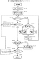
【0034】
図6は、第1の実施の形態例の消去フローチャート図である。また、図7は、第1の実施の形態例の消去動作の例を示す図表である。図5に示したメモリの例に、図6の消去フローチャートを適用した場合の状態の変化が、図7に示される。
【0035】
第1の実施の形態例では、最初の消去ストレスは、4つのメモリブロックに対して同時に印加される。また、最初の消去ベリファイ対象のメモリブロックは、過去の消去ストレス値(回数)が最小のメモリブロックBL4に設定される。そして、4つのメモリブロックに同時に消去ストレスを印加しながら、最小消去ストレス値を有するメモリブロックBL4に対して消去ベリファイを行い、同時消去ストレス回数が最小値EN4に達するか、或いはメモリブロックBL4の全てのメモリセルが消去ベリファイをパスするまで、消去ストレスの同時印加を継続する。消去ストレス回数が最小値に達するか或いはメモリブロックBL4の全てのメモリセルが消去ベリファイをパスすると、複数メモリブロックに対する同時消去ストレスの印加を止め、メモリブロック毎に消去ストレスの印加と消去ベリファイを行う。
【0036】
図6に示される通り、まず最初に、全ての消去対象のメモリブロックに対してデータ0をプログラムするプリ・プログラムが行われる(S10)。そして、過去の消去ストレス値(回数)が最小のメモリブロックBL4を消去ベリファイ対象として設定する(S11)。即ち、メモリブロックアドレスを、メモリブロックBL4に設定する。そして、メモリブロックBL4のメモリセルの閾値が、消去ベリファイレベルVEより低くなったか否かを確認する消去ベリファイが行われる(S12)。具体的には、ワード線に消去ベリファイレベルVEの電圧を印加したときに、対応するビット線に所定の電流が流れるか否かをチェックすることで行われる。
【0037】
最初は、消去ストレスは印加されていないので、消去ベリファイはフェイル(未確認)となる。更に、最初は、消去ストレスの回数が最小消去ストレス値よりも少ないので(S14)、複数ブロック選択モードとなり(S16)、4つのメモリブロック全てに対して、同時に単位時間の消去ストレスの印加が行われる(S20)。4つのメモリブロックへの消去ストレスの同時印加は、最小消去ストレス値(回数)EN4まで繰り返される。
【0038】
また、一方で、メモリブロックBL4内の最初のアドレスのメモリセルが消去ベリファイをパス(閾値電圧が消去ベリファイレベルVEより低くなる)すると(S12)、そのメモリブロック内の最終アドレスに達するまで(S22)、メモリセルのアドレスがインクリメントされ、消去ストレスの複数ブロックへの同時印加(S16)が繰り返される。
【0039】
従って、4つのメモリブロックへの消去ストレスの同時印加の回数が最小値EN4に達するか、或いは、最小消去ストレス値に対応するメモリブロックBL4の全てのメモリセルの消去ベリファイが完了するかのうち、いずれか少ない回数まで、上記の4つのメモリブロックへの消去ストレスの同時印加が繰り返される。その結果、過去において最小消去ストレス値であるメモリブロックBL4の消去ストレス値が、図4に示される通り低下してもオーバーイレーズされることが避けられる。また、図4に示される通り、消去ストレス値が増加する場合は、当然にオーバーイレーズされることは避けられる。
【0040】
図7に示された例では、消去ストレスの印加回数がメモリブロックBL4の最小値EN4に達するまで、メモリブロックBL4内の全てのメモリセルの消去ベリファイが終了していない。従って、消去ストレスの印加回数が最小値EN4を超えると、メモリブロック毎に消去ストレスの印加と消去ベリファイとが行われる。即ち、図6のフローチャートのステップS18に示される通り、複数ブロック選択モードが解除されて、消去ベリファイの対象のメモリブロックBL4への消去ストレスの印加が行われる(S20)。
【0041】
やがて、メモリブロックBL4内の全てのメモリセルの閾値が消去ベリファイレベルVE未満となると、最終アドレスとなり(S22)、ブロックアドレスがインクリメントされる(S32)。尚、メモリブロックBL4に対して印加された消去ストレスの回数が、前回の最小値EN4より少ない場合は、その最小値は、新しい値に更新される。或いは、後に消去ベリファイされた他のメモリブロックBL1〜BL3の消去ストレス回数が前回のメモリブロックBL4の最小値EN4よりも少ない場合は、その最小値と最小値ブロックが更新される(S26,S28)。
【0042】
図7に示される通り、ブロックアドレスがインクリメントされたことにより、メモリブロックBL1が消去動作の対象ブロックとなる。メモリブロックBL1に対して消去ストレスを印加しながら(S20)、メモリブロックBL1内のメモリセルの消去ベリファイが行われる(S12)。全てのメモリセルが消去ベリファイをパスすると、ブロックアドレスがインクリメントされ、今度は、メモリブロックBL2が消去の対象ブロックとなる。以下、メモリブロックBL2とBL3に対して、それぞれブロック毎に消去ストレスの印加と、消去ベリファイが行われる。最後のメモリブロックBL3の最終アドレスまで消去ベリファイが行われると、消去動作が終了する。
【0043】
以上の通り、第1の実施の形態例では、過去の消去動作または製品出荷前の試験における消去動作において、各メモリブロックの消去ストレス値(回数)を記憶し、消去動作時において、その最小値に達するまで複数メモリブロックに対して同時に消去ストレスを印加する。或いは、最小値に対応するメモリブロックの全てのメモリセルの消去ベリファイが終了するまで複数メモリブロックに対して同時に消去ストレスを印加する。その後は、各メモリブロック毎に消去ストレスの印加と消去ベリファイを行う。従って、メモリブロック間において必要な消去ストレス値にバラツキがあっても、オーバーイレーズが発生する確率を少なくすることができる。また、図5に示される様に、消去に必要な消去ストレス値(回数)が変化しても、オーバーイレーズをする可能性を少なくすることができる。特に、各メモリセルの消去特性は一定の傾向を有し、過去において最小のストレス回数で消去できたメモリセルは、次の消去時においても最小のストレス回数で消去できる傾向を有する。更に、上記の実施の形態例では、複数のメモリブロックに対して同時に消去ストレスを印加するので、全体の消去時間を短くすることができる。
【0044】
図8は、第2の実施の形態例の消去フローチャート図である。また、図9は、第2の実施の形態例の消去動作の例を示す図表である。図5に示したメモリの例に、図8の消去フローチャートを適用した場合の状態の変化が、図9に示される。
【0045】
第2の実施の形態例では、全てのメモリブロックの過去における消去ストレス値(回数)を記憶しておく。そして、消去時は、それぞれのメモリブロックの過去の消去ストレス値(回数)に達するまで、他のメモリブロックと同時に消去ストレスが印加される。従って、最初の消去ストレスは、全てのメモリブロックに同時に印加され、その後、過去の消去ストレス値に達したメモリブロックから順に消去ストレスの同時印加のグループから解除される。また、消去ベリファイの対象は、第1の実施の形態例の如く最小消去ストレス値のメモリブロックから開始することが好ましいが、任意のメモリブロックから開始しても良い。即ち、第2の実施の形態例では、過去の消去ストレス値を優先して、複数のメモリブロックに同時に消去ストレスを印加し、それぞれのメモリブロックの過去の消去ストレス値に達っしたら同時印加の対象から解除する。但し、最小消去ストレス値のメモリブロックから消去ベリファイすることで、第1の実施の形態例と同様に、必要な消去ストレス値(回数)が減少する傾向にある場合は、その分オーバーイレーズを防止することが可能になる。消去ストレスの同時印加が終わると、その後は、各メモリブロック毎に消去ストレスの印加と消去ベリファイを行う。
【0046】
図5のメモリについてこの消去方法を適用した例を、図8,9を参照しながら説明する。図8に示される通り、最初に全てのメモリセルに対して、プリプログラムを行い、全てのメモリセルの閾値電圧をプログラムベリファイレベルVPより高くする(S40)。そして、任意のメモリブロックを消去ベリファイ対象とし、4つのメモリブロックを消去ストレス印加対象とする(S41)。ここでは、消去ベリファイ対象をメモリブロックBL1とする。
【0047】
消去ベリファイにおいて、確認対象のメモリセルの閾値電圧が消去ベリファイレベルVEより低くない場合は(S42)、消去ストレス値(回数)がそれぞれのメモリブロックの過去の消去ストレス値に達するまで(S44)、複数ブロックを選択した状態で(S46)、消去ストレスを印加する(S50)。図9に示される通り、消去ストレス回数が1回からEN4回までは、4つのメモリブロックBL1〜BL4に対して、消去ストレスが同時に印加される。
【0048】
消去ストレスの印加回数がメモリブロックBL4の過去の回数EN4に達すると、ステップS44で検出され、メモリブロックBL4は選択から解除される(S48)。その結果、その後の消去ストレスの印加は、メモリブロックBL1,BL2,BL3に対して同時に行われる。
【0049】
図9の例では、やがてメモリブロックBL1の全てのメモリセルが消去ベリファイをパスし、消去ベリファイ対象ブロック内のアドレスが最終アドレスに達したことが検出される(S52)。このメモリブロックBL1に対する消去ストレス値(回数)が過去の回数よりも少なくなっている場合は(S56)、図4に示される通り消去ストレス値が減少する段階に該当し、消去ストレス値(回数)が更新される(S58)。これにより、常に最小の値が記憶される。そして、最終ブロックアドレスでなければ(S60)、ブロックアドレスがインクリメントされ、メモリブロックBL2が消去ベリファイの対象となる(S62)。更に、消去ベリファイが完了したメモリブロックBL1は、もはや消去ストレスを印加する必要がないので、選択から解除される(S62)。
【0050】
その結果、図9に示される通り、消去ストレスの印加は、メモリブロックBL2,BL3に対して同時に行われ、消去ベリファイ対象はメモリブロックBL2となる。図9の例では、メモリブロックBL2の消去ベリファイが終了する前に、メモリブロックBL3の過去の消去ストレス回数EN3に達っしたことがステップS44で検出され、メモリブロックBL3の選択が解除される(S48)。その結果、消去ストレスの印加(S50)は、メモリブロックBL2のみとなり、そのメモリブロックBL2に対して消去ベリファイが継続される。
【0051】
やがて、メモリブロックBL2の消去ベリファイが終了すると(S42,S52)、メモリブロックBL2も選択から解除され、消去ベリファイ対象のメモリブロックのブロックアドレスがインクリメントされ、メモリブロックBL3が消去ベリファイの対象となる(S62)。
【0052】
そして、ステップS43にて、全てのメモリブロックが選択から解除されたことが検出されると、その後は、消去ベリファイ対象のメモリブロックに対して、消去ストレスが印加される(S45,S50)。即ち、メモリブロック毎に消去ストレスの印加と消去ベリファイとが繰り返し行われ、それぞれのメモリブロックの消去ベリファイが終了する度に、消去対象のメモリブロックが変更される。
【0053】
尚、第1の実施の形態例と同様に、従って、最初の消去ベリファイ対象ブロックを、過去の消去ストレス値(回数)が最小のメモリブロックBL4にする場合は、図4の如く消去ストレス値が減少する段階にある時は、メモリブロックBL4に対する消去ストレスの印加が過去の回数EN4に達する前に消去ベリファイが終了する可能性が高くなる。オーバーイレーズを防止することができより好ましい。
【0054】
上記の消去動作を制御する消去回路32(図1参照)は、例えば、簡易的なマイクロコンピュータにより構成されることができる。即ち、図6または図8に示される消去フローチャートに基づく消去プログラムを格納したROMと、それを実行する演算回路とを有する一般的なマイクロコンピュータにより実現することができる。その場合、過去の消去ストレス値が消去回路に内蔵される不揮発性メモリに記憶される。
【0055】
図10は、かかる消去回路の構成図である。図10の消去回路32は、CPU321と、消去プログラムを格納したROM322と、消去ストレス値が記憶される不揮発性メモリ323と、インターフェース325とがバス324を介して接続される。
【0056】
上記実施の形態例では、消去ストレス値として、単位時間の消去ストレス印加の回数で説明したが、消去ストレスの印加時間であっても良い。或いは、消去ストレスの強さを考慮した値であっても良い。
【0057】
【発明の効果】
以上説明した通り、本発明によれば、消去ストレスの印加を過去の消去ストレス値に基づいて複数メモリブロックに対して同時に行い、その後は、メモリブロック毎に消去ストレスの印加と消去ベリファイを繰り返し行う。その結果、オーバーイレーズが発生する確率を低く抑えることができるとともに、消去動作全体の時間を短くすることができる。
【図面の簡単な説明】
【図1】本発明の対象である不揮発性メモリの全体構成図である。
【図2】本発明の対象である一般的な不揮発性メモリの回路図である。
【図3】消去動作の概略を示す図である。
【図4】消去ストレス回数の変化を示す図である。
【図5】消去動作を説明するための複数メモリブロックと消去ストレス回数の例を示す図である。
【図6】第1の実施の形態例の消去フローチャート図である。
【図7】第1の実施の形態例の消去動作の例を示す図表である。
【図8】第2の実施の形態例の消去フローチャート図である。
【図9】第2の実施の形態例の消去動作の例を示す図表である。
【図10】消去回路の構成図である。
【符号の説明】
32 消去回路
BL1〜BL4 メモリブロック
MC メモリセル[0001]
BACKGROUND OF THE INVENTION
The present invention relates to a non-volatile memory device such as a flash memory, and more particularly to a non-volatile memory device that prevents over-erasing and shortens an erasing time.
[0002]
[Prior art]
An electrically rewritable nonvolatile memory device such as a flash memory or an EEPROM can hold stored data in the absence of a power source and is widely used in mobile phones, portable information terminals, and the like. In particular, flash memories have been increasing in storage capacity, and erasure is performed in units of large-capacity memory blocks.
[0003]
A memory cell of a nonvolatile memory generally has a control gate connected to a word line, a drain connected to a bit line, and a source connected to a source line. Then, a high voltage is applied to the control gate and the drain to turn on the transistor of the memory cell, the source is set to a low voltage, and electrons passing through the channel are injected into the floating gate, thereby programming operation (
[0004]
In the erase operation, the control gate is set to a low voltage or a negative voltage, the drain is floated, and the source is set to a high voltage, whereby electrons are extracted from the floating gate. Application of a predetermined voltage to such a memory cell is referred to as application of erasing stress. When the erase operation is performed, the transistor of the memory cell has a low threshold voltage.
[0005]
In the read operation, by controlling the word line to a voltage intermediate between the threshold voltages of the programmed and erased memory cells, the transistor of the memory cell in the programmed state is non-conductive and the transistor of the memory cell in the erased state is conductive. The presence or absence of current due to non-conduction and conduction is detected via the bit line.
[0006]
In the erase operation, after applying the above-described erase stress for a predetermined unit time, the memory cell to be erased is read to check whether the threshold voltage has become lower than the erase verify level (verify). An appropriate erase operation is performed by repeatedly applying the erase stress and erase verify. In a flash memory using a non-volatile memory, an erasing operation is performed collectively for each memory block having a plurality of memory cells.
[0007]
[Problems to be solved by the invention]
In the above erasing operation, if an unnecessarily large amount of erasing stress is applied, the threshold voltage of the memory cell transistor becomes negative, and the memory connected to the word line is not selected (L level). The cell becomes conductive, which is not preferable. Such a state is called over-erase (over-erasure) and is a state that must be avoided in the erase operation.
[0008]
On the other hand, with an increase in memory capacity, the number of erase stresses or time variations required for each memory cell or memory block tends to increase. In general, in the erasing operation, erasing stress is applied to a plurality of memory cells at once, and erasing verification is performed in units of memory cells. Therefore, even if the erasure of some memory cells is completed, if the erasure of other memory cells is not completed, the erasure stress is applied collectively to the memory cells that have been erased. As a result, some memory cells are overerased. The greater the number of memory cells to which erase stress is applied at once, the greater the degree of variation in the number of erase stresses required for them, and the higher the probability of overerase.
[0009]
In order to avoid such an over-erase problem, conventionally, a memory area is divided into a plurality of memory blocks, and application of erase stress and erase verification are repeatedly performed for each memory block. By reducing the number of memory cells to be erased at once, variation in the threshold voltage of the memory cells after application of erasing stress can be suppressed, and the problem of over-erasing can be avoided.
[0010]
However, according to the method of repeatedly applying erase stress and erase verify for each memory block, it takes a long time to erase all of the plurality of memory blocks. In particular, in a flash memory whose capacity is increasing, such a long erase time is a problem to be solved.
[0011]
SUMMARY OF THE INVENTION An object of the present invention is to provide a non-volatile memory device that can prevent over-erasing and shorten the erase time.
[0012]
It is another object of the present invention to provide a non-volatile memory device that has a low probability of over-erasing due to erasing and a short erasing time for a large-capacity memory.
[0013]
[Means for Solving the Problems]
In order to achieve the above object, the present invention provides a nonvolatile memory device in which carriers are injected into or removed from a floating gate of a memory cell to program or erase the memory cell.
A plurality of memory blocks each having a plurality of memory cells;
An erasing circuit that applies erasing stress in units of memory blocks and performs erasing end verification in units of memory cells;
The erasing circuit is configured to reduce a past erasing stress minimum value in the plurality of memory blocks. , Erase stress is applied to multiple memory blocks at the same time while performing erase verify only on the memory block having the past minimum erase stress value. Then, erase stress application and erase end verification are performed for each memory block. It is characterized by that.
[0014]
According to the above invention, the erase stress value such as the number of erase stresses for each memory block when the erase operation has been performed in the past is recorded, and the minimum erase stress value among those erase stress values is recorded. At the next erasing, erasing stress is applied to the plurality of memory blocks at a time until the minimum erasing stress value is reached. As a result, the erase time can be shortened as compared with the conventional method in which the application of the erase stress and the erase verify are repeated for each memory block.
[0015]
Furthermore, the present invention is characterized in that after the simultaneous erasing stress is applied to the plurality of memory blocks, the erasing stress is applied and the erasure verification is performed for each memory block.
[0016]
According to the above invention, after the threshold voltage of the memory cell becomes close to the erase verify level, the application of the erase stress and the erase verify are repeated for each memory block, so that the number of memory cells to be collectively erased is reduced. And the probability of overerasing can be reduced.
[0017]
DETAILED DESCRIPTION OF THE INVENTION
Hereinafter, embodiments of the present invention will be described with reference to the drawings. However, the technical scope of the present invention is not limited to the embodiment.
[0018]
FIG. 1 is an overall configuration diagram of a nonvolatile memory cell. The nonvolatile memory device shown in FIG. 1 has a memory
[0019]
The
[0020]
One feature of the nonvolatile memory device is that a predetermined voltage is applied to each word line, bit line, and source line during a program operation and an erase operation, as described in the prior art. For this purpose, a
[0021]
The
[0022]
FIG. 2 is a circuit diagram of the nonvolatile memory. FIG. 2 shows a memory
[0023]
In FIG. 2, a total of four memory cells MC00, MC01, MC10, MC11 of 2 rows and 2 columns are shown in the memory
[0024]
Such programming, erasing, and reading operations for the nonvolatile memory are performed by applying predetermined voltages to the word lines WL, bit lines BL, and source lines SL, as shown in the table at the bottom of FIG. . Assume that memory cell MC00 is programmed. In that case, a high voltage (HH level) is applied to the word line WL0, a high voltage (HH level) is applied to the bit line BL0, and a low voltage (L level) is applied to the source line SL. As a result, the transistor of the memory cell MC00 becomes conductive, and electrons passing through the channel region are injected into the floating gate by an electric field formed between the control gate and the source region. As a result, the threshold voltage of the memory cell MC00 increases.
[0025]
Next, if the memory cell MC11 is erased, a negative voltage is applied to the word line WL1, the bit line BL1 is floated, and a high voltage (H level) is applied to the source line SL. As a result, an electric field in the opposite direction to that during programming is applied between the control gate and the source region, and electrons in the floating gate are removed. As a result, the threshold voltage of the memory cell MC11 is lowered. At this time, a negative voltage is simultaneously applied to the word line WL0, and all the memory cells MC00, MC01, MC10 are simultaneously erased.
[0026]
FIG. 3 is a diagram showing an outline of the erase operation. In FIG. 3A, the horizontal axis indicates the threshold voltage Vth of the memory cell, the vertical axis indicates the number of memory cells, some of the memory cells in the memory cell matrix are in the programmed state, and the remaining memory cells are erased. The distribution in the case of a state is shown. The memory cells in the programmed state are located in the distribution PR, and the threshold voltage of each memory cell is higher than the program verify level VP. On the other hand, the memory cells in the erased state are in the distribution ER, and the threshold voltage of these memory cells is lower than the erase verify level VE. At the time of reading, by controlling the word line to the read level VR, the memory cell in the programmed state becomes non-conductive and the memory cell in the erased state becomes conductive. The presence / absence of such current is detected by the sense amplifier SA via the
[0027]
The erasing operation of the nonvolatile memory is collectively performed on a plurality of memory cells. The general erase operation is as follows. First, as shown in FIG. 3B,
[0028]
Here, if the number of memory cells to which erase stress is applied at once is large, as shown by the solid line in FIG. 3C, the variation in the threshold voltage of the memory cells after the erase operation ends increases. Some memory cells (shaded lines in the figure) have a negative threshold voltage and are in an overerased state.
[0029]
When the threshold voltage of the memory cell becomes negative, normal read operation cannot be performed. For example, in FIG. 2, it is assumed that the memory cell MC01 is in the erased state (data 1) and the memory cell MC11 is in the overerased state. When the word line WL0 is raised to the read level and
[0030]
As described above, in the erase operation of the nonvolatile memory, it is necessary that the threshold voltage of the memory cell is lower than the erase verify level VE and does not become negative. Conventionally, in order to reduce the probability of such over-erasing, a unit for collectively applying an erasing stress is set as a memory block unit, and as shown by a broken line in FIG. 3C, variation in threshold voltage of the memory cell is reduced. ing.
[0031]
FIG. 4 is a diagram showing changes in the number of erasure stresses. In FIG. 4, the horizontal axis indicates the number of times of erasing, and the vertical axis indicates the number of times of stress application (stress value) necessary for erasing, and shows the tendency of changes in the number of stresses necessary for erasing a general nonvolatile memory. As shown in FIG. 4, every time the number of erasures increases in the initial stage, the number of stresses necessary for erasure decreases, and when the number of erasures further increases, the number of stresses necessary for erasure increases. As described above, the number of erasing stresses necessary for erasing the nonvolatile memory changes sequentially as the number of erasing times increases.
[0032]
Next, the erase operation according to the embodiment of the present invention will be described. Also in the present embodiment, the erasing circuit can apply erasing stress to each of the memory blocks divided into a plurality, as in the conventional case. The erase verify is performed for each memory cell as in the conventional example. In this embodiment, in the erase operation, first, erase stress is simultaneously applied to a plurality of memory blocks. The number of times erasing stress is applied simultaneously is the minimum number of erasing stresses among the number of erasing stresses required for each of the plurality of memory blocks. Thereafter, application of erase stress and erase verify are repeated for each memory block. Alternatively, an erasing stress is applied simultaneously to a plurality of memory blocks as appropriate.
[0033]
FIG. 5 is a diagram illustrating an example of a plurality of memory blocks and the number of erase stresses for explaining the erase operation. In the example of FIG. 5, the memory 100 is divided into four memory blocks BL1 to BL4. The erase stress values (number of erase stresses) required in the past erase operation in each memory block are EN1 to EN4, and the magnitude relationship between the erase stress values is as shown in FIG. That is, the past erase stress value EN2 of the memory block BL2 is the longest (large), and the past required erase stress value EN4 of the memory block BL4 is the smallest. The erasing operation of the embodiment of the present invention will be described by taking the memory shown in FIG. 5 as an example.
[0034]
FIG. 6 is an erasing flowchart diagram of the first embodiment. FIG. 7 is a chart showing an example of the erasing operation of the first embodiment. FIG. 7 shows a change in state when the erasing flowchart of FIG. 6 is applied to the example of the memory shown in FIG.
[0035]
In the first embodiment, the initial erase stress is applied simultaneously to the four memory blocks. In addition, the first memory block to be erase-verified is set to the memory block BL4 having the smallest erase stress value (number of times) in the past. Then, erase verify is performed on the memory block BL4 having the minimum erase stress value while simultaneously applying erase stress to the four memory blocks, and the number of simultaneous erase stresses reaches the minimum value EN4 or all of the memory blocks BL4 The erase stress is simultaneously applied until the memory cell passes the erase verify. When the number of erase stresses reaches the minimum value or all memory cells in the memory block BL4 pass the erase verify, the application of the simultaneous erase stress to the plurality of memory blocks is stopped, and the application of the erase stress and the erase verify are performed for each memory block. .
[0036]
As shown in FIG. 6, first, pre-programming for
[0037]
Initially, since erase stress is not applied, erase verify is failed (unconfirmed). Furthermore, initially, since the number of erase stresses is less than the minimum erase stress value (S14), the multi-block selection mode is set (S16), and the unit time erase stress is simultaneously applied to all four memory blocks. (S20). The simultaneous application of the erase stress to the four memory blocks is repeated up to the minimum erase stress value (number of times) EN4.
[0038]
On the other hand, when the memory cell at the first address in the memory block BL4 passes the erase verify (threshold voltage becomes lower than the erase verify level VE) (S12), until the final address in the memory block is reached (S22). ) The address of the memory cell is incremented, and the simultaneous application of erase stress to a plurality of blocks (S16) is repeated.
[0039]
Accordingly, whether the number of simultaneous application of erase stress to the four memory blocks reaches the minimum value EN4, or whether erase verify of all the memory cells in the memory block BL4 corresponding to the minimum erase stress value is completed. The erasing stress is simultaneously applied to the four memory blocks up to the smaller number of times. As a result, even if the erase stress value of the memory block BL4, which is the minimum erase stress value in the past, decreases as shown in FIG. Further, as shown in FIG. 4, when the erase stress value increases, it is naturally avoided that the erase is overerased.
[0040]
In the example shown in FIG. 7, the erase verify of all the memory cells in the memory block BL4 is not completed until the number of times of application of the erase stress reaches the minimum value EN4 of the memory block BL4. Therefore, when the number of times of application of erase stress exceeds the minimum value EN4, application of erase stress and erase verification are performed for each memory block. That is, as shown in step S18 of the flowchart of FIG. 6, the multiple block selection mode is canceled and erasure stress is applied to the memory block BL4 to be erase verified (S20).
[0041]
Eventually, when the threshold values of all the memory cells in the memory block BL4 become less than the erase verify level VE, the final address is reached (S22), and the block address is incremented (S32). When the number of erase stresses applied to the memory block BL4 is smaller than the previous minimum value EN4, the minimum value is updated to a new value. Alternatively, when the number of erase stresses of other memory blocks BL1 to BL3 that have been erase-verified later is smaller than the minimum value EN4 of the previous memory block BL4, the minimum value and minimum value blocks are updated (S26, S28). .
[0042]
As shown in FIG. 7, when the block address is incremented, the memory block BL1 becomes the target block for the erase operation. While applying erase stress to the memory block BL1 (S20), erase verify of the memory cells in the memory block BL1 is performed (S12). When all the memory cells pass the erase verify, the block address is incremented, and this time, the memory block BL2 becomes the block to be erased. Hereinafter, erase stress is applied to each of the memory blocks BL2 and BL3 and erase verify is performed for each block. When the erase verify is performed up to the final address of the last memory block BL3, the erase operation is finished.
[0043]
As described above, in the first embodiment, the erase stress value (number of times) of each memory block is stored in the past erase operation or the erase operation in the test before product shipment, and the minimum value is obtained during the erase operation. Erasing stress is simultaneously applied to a plurality of memory blocks until the value reaches. Alternatively, erase stress is simultaneously applied to a plurality of memory blocks until the erase verify of all the memory cells in the memory block corresponding to the minimum value is completed. Thereafter, application of erase stress and erase verify are performed for each memory block. Therefore, even if the required erase stress value varies between memory blocks, the probability of overerasing can be reduced. Further, as shown in FIG. 5, even if the erasing stress value (number of times) necessary for erasing changes, the possibility of overerasing can be reduced. In particular, the erase characteristic of each memory cell has a certain tendency, and a memory cell that can be erased with the minimum number of stresses in the past tends to be erased with the minimum number of stresses at the next erase time. Furthermore, in the above embodiment, the erasing stress is simultaneously applied to a plurality of memory blocks, so that the entire erasing time can be shortened.
[0044]
FIG. 8 is an erasing flowchart according to the second embodiment. FIG. 9 is a table showing an example of the erasing operation of the second embodiment. FIG. 9 shows a change in state when the erasing flowchart of FIG. 8 is applied to the example of the memory shown in FIG.
[0045]
In the second embodiment, erasing stress values (number of times) in the past of all memory blocks are stored. At the time of erasing, erasing stress is applied simultaneously with other memory blocks until the past erasing stress value (number of times) of each memory block is reached. Therefore, the first erase stress is simultaneously applied to all the memory blocks, and thereafter, the memory blocks that have reached the past erase stress value are released from the simultaneous erase stress simultaneous application group. The target of the erase verify is preferably started from a memory block having the minimum erase stress value as in the first embodiment, but may be started from an arbitrary memory block. That is, in the second embodiment, priority is given to past erase stress values, and erase stress is simultaneously applied to a plurality of memory blocks. When the past erase stress values of the respective memory blocks are reached, simultaneous application is performed. Release from the target. However, if the required erase stress value (number of times) tends to decrease by performing erase verify from the memory block having the minimum erase stress value, as in the first embodiment, over-erasure is prevented accordingly. It becomes possible to do. After the simultaneous application of the erase stress is finished, the erase stress is applied and erase verify is performed for each memory block.
[0046]
An example in which this erasing method is applied to the memory of FIG. 5 will be described with reference to FIGS. As shown in FIG. 8, first, all memory cells are pre-programmed, and the threshold voltages of all memory cells are made higher than the program verify level VP (S40). Then, an arbitrary memory block is set as an erase verify target, and four memory blocks are set as an erase stress application target (S41). Here, the erase verify target is the memory block BL1.
[0047]
In the erase verify, when the threshold voltage of the memory cell to be confirmed is not lower than the erase verify level VE (S42), until the erase stress value (number of times) reaches the past erase stress value of each memory block (S44). With a plurality of blocks selected (S46), erase stress is applied (S50). As shown in FIG. 9, when the number of erase stresses is from 1 to EN4, erase stress is simultaneously applied to the four memory blocks BL1 to BL4.
[0048]
When the number of erase stresses applied reaches the past number EN4 of the memory block BL4, it is detected in step S44, and the memory block BL4 is deselected (S48). As a result, the subsequent erase stress is simultaneously applied to the memory blocks BL1, BL2, and BL3.
[0049]
In the example of FIG. 9, it is detected that all the memory cells in the memory block BL1 eventually pass the erase verify and the address in the erase verify target block has reached the final address (S52). When the erase stress value (number of times) for the memory block BL1 is smaller than the past number of times (S56), this corresponds to the stage where the erase stress value decreases as shown in FIG. 4, and the erase stress value (number of times). Is updated (S58). Thereby, the minimum value is always stored. If it is not the final block address (S60), the block address is incremented, and the memory block BL2 is subjected to erase verification (S62). Further, the memory block BL1 for which the erase verify has been completed is released from the selection because it is no longer necessary to apply the erase stress (S62).
[0050]
As a result, as shown in FIG. 9, the erase stress is applied to the memory blocks BL2 and BL3 simultaneously, and the erase verify target is the memory block BL2. In the example of FIG. 9, before the erase verify of the memory block BL2 is completed, it is detected in step S44 that the past erase stress count EN3 of the memory block BL3 has been reached, and the selection of the memory block BL3 is canceled ( S48). As a result, the erase stress is applied only to the memory block BL2 (S50), and erase verify is continued for the memory block BL2.
[0051]
Eventually, when erase verify of the memory block BL2 is completed (S42, S52), the memory block BL2 is also deselected, the block address of the memory block to be erase verified is incremented, and the memory block BL3 is subject to erase verify ( S62).
[0052]
Then, when it is detected in step S43 that all the memory blocks are released from the selection, thereafter, an erasure stress is applied to the memory block to be erase verified (S45, S50). That is, application of erase stress and erase verification are repeatedly performed for each memory block, and each time the erase verification of each memory block is completed, the memory block to be erased is changed.
[0053]
As in the first embodiment, therefore, when the first erase verify target block is the memory block BL4 having the smallest erase stress value (number of times), the erase stress value is as shown in FIG. When it is in the decreasing stage, there is a high possibility that the erase verify is completed before the application of the erase stress to the memory block BL4 reaches the past number of times EN4. Overerasing can be prevented, which is more preferable.
[0054]
The erasing circuit 32 (see FIG. 1) for controlling the erasing operation can be constituted by a simple microcomputer, for example. That is, it can be realized by a general microcomputer having a ROM storing an erasing program based on the erasing flowchart shown in FIG. 6 or 8 and an arithmetic circuit for executing the ROM. In that case, past erase stress values are stored in a non-volatile memory built in the erase circuit.
[0055]
FIG. 10 is a block diagram of such an erasing circuit. In the erasing
[0056]
In the above embodiment, the erase stress value has been described as the number of times of erase stress application per unit time, but it may be the erase stress application time. Alternatively, it may be a value considering the strength of erasure stress.
[0057]
【The invention's effect】
As described above, according to the present invention, erase stress is applied simultaneously to a plurality of memory blocks based on past erase stress values, and thereafter, the erase stress is applied and erase verify is repeated for each memory block. . As a result, the probability of occurrence of overerasing can be kept low, and the entire erase operation time can be shortened.
[Brief description of the drawings]
FIG. 1 is an overall configuration diagram of a nonvolatile memory that is a subject of the present invention;
FIG. 2 is a circuit diagram of a general nonvolatile memory that is an object of the present invention.
FIG. 3 is a diagram schematically showing an erase operation.
FIG. 4 is a diagram showing a change in the number of erase stresses.
FIG. 5 is a diagram illustrating an example of a plurality of memory blocks and the number of erase stresses for explaining an erase operation.
FIG. 6 is an erasing flowchart of the first embodiment.
FIG. 7 is a chart showing an example of an erasing operation according to the first embodiment.
FIG. 8 is an erasing flowchart of the second embodiment.
FIG. 9 is a chart showing an example of an erasing operation according to the second embodiment.
FIG. 10 is a configuration diagram of an erasing circuit.
[Explanation of symbols]
32 Erase circuit
BL1 to BL4 memory block
MC memory cell
Claims (6)
複数のメモリセルをそれぞれ有する複数のメモリブロックと、
前記メモリブロック単位で消去ストレスを印加し、メモリセル単位で消去終了のベリファイを行う消去回路とを有し、
前記消去回路は、前記複数のメモリブロックにおける過去の消去ストレス最小値まで、当該過去の消去ストレス最小値を有するメモリブロックのみに対して消去ベリファイを行いながら、該複数のメモリブロックに同時に消去ストレスを印加し、その後、前記メモリブロック毎に消去ストレスの印加と消去終了のベリファイを行うことを特徴とする不揮発性メモリ装置。In a nonvolatile memory device in which a memory cell is programmed or erased by injecting or removing carriers into the floating gate of the memory cell,
A plurality of memory blocks each having a plurality of memory cells;
An erasing circuit that applies erasing stress in units of memory blocks and performs erasing end verification in units of memory cells;
The erase circuit performs erase verify on only the memory block having the past erase stress minimum value up to the past erase stress minimum value in the plurality of memory blocks, and simultaneously applies erase stress to the plurality of memory blocks. The nonvolatile memory device is characterized in that, after applying, erase stress is applied to each of the memory blocks and erase completion is verified.
複数のメモリセルをそれぞれ有する複数のメモリブロックと、
前記メモリブロック単位で消去ストレスを印加し、メモリセル単位で消去終了のベリファイを行う消去回路とを有し、
前記消去回路は、前記複数のメモリブロックにおける過去の消去ストレス最小値までもしくは前記消去ストレス最小値に対応するメモリブロック内の全てのメモリセルの消去終了ベリファイが行われるまで、当該過去の消去ストレス最小値を有するメモリブロックのみに対して消去ベリファイを行いながら、該複数のメモリブロックに同時に消去ストレスを印加し、その後、前記メモリブロック毎に消去ストレスの印加と消去終了のベリファイを行うことを特徴とする不揮発性メモリ装置。In a nonvolatile memory device in which a memory cell is programmed or erased by injecting or removing carriers into the floating gate of the memory cell,
A plurality of memory blocks each having a plurality of memory cells;
An erasing circuit that applies erasing stress in units of memory blocks and performs erasing end verification in units of memory cells;
The erasing circuit has the past erase stress minimum until the past erase stress minimum value in the plurality of memory blocks or the erase end verification of all the memory cells in the memory block corresponding to the erase stress minimum value is performed. An erase stress is simultaneously applied to the plurality of memory blocks while performing erase verify only on the memory block having a value, and thereafter, erase stress is applied to each of the memory blocks and erase end verification is performed. A non-volatile memory device.
複数のメモリセルをそれぞれ有する複数のメモリブロックと、
前記メモリブロック単位で消去ストレスを印加し、メモリセル単位で消去終了のベリファイを行う消去回路とを有し、
前記消去回路は、前記複数のメモリブロックにおける過去の消去ストレス最小値までもしくは前記消去ストレス最小値に対応するメモリブロック内の全てのメモリセルの消去終了ベリファイが行われるまで、当該過去の消去ストレス最小値を有するメモリブロックのみに対して消去ベリファイを行いながら、該複数のメモリブロックに同時に消去ストレスを印加し、その後、前記メモリブロック毎に消去ストレスの印加と消去終了のベリファイを行い、更に、
前記消去回路は、前記消去ストレス最小値に対応するメモリブロックの消去が、過去の消去ストレス最小値よりも小さい消去ストレスで完了した時は、当該消去ストレス最小値を更新することを特徴とする不揮発性メモリ装置。In a nonvolatile memory device in which a memory cell is programmed or erased by injecting or removing carriers into the floating gate of the memory cell,
A plurality of memory blocks each having a plurality of memory cells;
An erasing circuit that applies erasing stress in units of memory blocks and performs erasing end verification in units of memory cells;
The erase circuit, until erase end verification of all the memory cells in the memory block corresponding to the past erase or said erasing stress minimum stress to a minimum value in said plurality of memory blocks is performed, the past erasing stress minimum While performing erase verify only on memory blocks having values , simultaneously applying erase stress to the plurality of memory blocks, then applying erase stress and verifying completion of erase for each memory block, and
The erase circuit updates the erase stress minimum value when the erase of the memory block corresponding to the erase stress minimum value is completed with an erase stress smaller than the past erase stress minimum value. Memory device.
複数のメモリセルをそれぞれ有する複数のメモリブロックと、
前記メモリブロック単位で消去ストレスを印加し、メモリセル単位で消去終了のベリファイを行う消去回路とを有し、
前記消去回路は、前記複数のメモリブロックそれぞれに対し、それぞれの過去の消去ストレス値まで消去ストレスを同時に印加しながら、当該同時消去ストレス印加中に、過去の消去ストレス最小値を有するメモリブロックのみに対し消去ベリファイを行い、前記消去終了ベリファイが全てのメモリセルに対して行われた第1のメモリブロックへの消去ストレスの印加を終了し、更に前記過去の消去ストレス値に達した第2のメモリブロックへの消去ストレスの印加を一旦終了し、その後、前記第2のメモリブロックに対してメモリブロック毎に消去ストレスの印加と消去終了のベリファイを行い、更に、
前記消去回路は、前記メモリブロックの消去が、対応する過去の消去ストレス値よりも小さい消去ストレス値で完了した時は、当該メモリブロックの消去ストレス値を更新することを特徴とする不揮発性メモリ装置。In a nonvolatile memory device in which a memory cell is programmed or erased by injecting or removing carriers into the floating gate of the memory cell,
A plurality of memory blocks each having a plurality of memory cells;
An erasing circuit that applies erasing stress in units of memory blocks and performs erasing end verification in units of memory cells;
The erasing circuit applies only erasing stress to each of the plurality of memory blocks to the past erasing stress value at the same time, and applies only to the memory block having the past erasing stress minimum value during the simultaneous erasing stress application. The erase verify is performed on the second memory, the erase stress is applied to the first memory block in which the erase end verify is performed for all the memory cells, and the second memory that has reached the past erase stress value is reached. The application of erase stress to the block is temporarily terminated, and then the erase stress is applied to the second memory block for each memory block and erase end verification is performed.
The erasing circuit updates the erasing stress value of the memory block when the erasing of the memory block is completed with an erasing stress value smaller than a corresponding past erasing stress value. .
前記消去ストレス値は、所定の単位消去ストレスの印加回数であることを特徴とする不揮発性メモリ装置。In any one of Claims 1 thru | or 4 ,
The non-volatile memory device according to claim 1, wherein the erase stress value is the number of times of applying a predetermined unit erase stress.
前記メモリセルは、ワード線に接続されたコントロールゲートと、ビット線に接続されたドレインと、ソース線に接続されたソースとを有し、
前記消去回路は、前記コントロールゲートとドレインとの間に電界を印加して、前記消去ストレスを印加することを特徴とする不揮発性メモリ装置。In any one of Claims 1 thru | or 4 ,
The memory cell has a control gate connected to a word line, a drain connected to a bit line, and a source connected to a source line,
The non-volatile memory device, wherein the erasing circuit applies the erasing stress by applying an electric field between the control gate and the drain.
Priority Applications (3)
| Application Number | Priority Date | Filing Date | Title |
|---|---|---|---|
| JP11224698A JP3672435B2 (en) | 1998-04-22 | 1998-04-22 | Nonvolatile memory device |
| US09/196,441 US5982670A (en) | 1998-04-22 | 1998-11-20 | Non-volatile memory device |
| KR1019980058053A KR100290195B1 (en) | 1998-04-22 | 1998-12-24 | Nonvolatile memory device |
Applications Claiming Priority (1)
| Application Number | Priority Date | Filing Date | Title |
|---|---|---|---|
| JP11224698A JP3672435B2 (en) | 1998-04-22 | 1998-04-22 | Nonvolatile memory device |
Publications (2)
| Publication Number | Publication Date |
|---|---|
| JPH11306769A JPH11306769A (en) | 1999-11-05 |
| JP3672435B2 true JP3672435B2 (en) | 2005-07-20 |
Family
ID=14581910
Family Applications (1)
| Application Number | Title | Priority Date | Filing Date |
|---|---|---|---|
| JP11224698A Expired - Fee Related JP3672435B2 (en) | 1998-04-22 | 1998-04-22 | Nonvolatile memory device |
Country Status (3)
| Country | Link |
|---|---|
| US (1) | US5982670A (en) |
| JP (1) | JP3672435B2 (en) |
| KR (1) | KR100290195B1 (en) |
Families Citing this family (27)
| Publication number | Priority date | Publication date | Assignee | Title |
|---|---|---|---|---|
| US6172915B1 (en) * | 1999-09-30 | 2001-01-09 | Eon Silicon Devices, Inc. | Unified erase method in flash EEPROM |
| KR100519534B1 (en) * | 2000-11-09 | 2005-10-05 | 주식회사 하이닉스반도체 | Method of erasing a flash memory device |
| US6331951B1 (en) * | 2000-11-21 | 2001-12-18 | Advanced Micro Devices, Inc. | Method and system for embedded chip erase verification |
| JP4071967B2 (en) | 2002-01-17 | 2008-04-02 | 株式会社ルネサステクノロジ | Nonvolatile semiconductor memory device and data erasing method thereof |
| US7149121B2 (en) * | 2005-01-26 | 2006-12-12 | Macronix International Co., Ltd. | Method and apparatus for changing operating conditions of nonvolatile memory |
| JP4903432B2 (en) | 2005-12-27 | 2012-03-28 | 株式会社東芝 | Nonvolatile semiconductor memory device |
| JP4983096B2 (en) * | 2006-05-24 | 2012-07-25 | 富士通セミコンダクター株式会社 | Nonvolatile semiconductor memory device, non-volatile semiconductor memory device erasing method, and non-volatile semiconductor memory device testing method |
| US7986553B2 (en) * | 2007-06-15 | 2011-07-26 | Micron Technology, Inc. | Programming of a solid state memory utilizing analog communication of bit patterns |
| US8659852B2 (en) | 2008-04-21 | 2014-02-25 | Seagate Technology Llc | Write-once magentic junction memory array |
| US7852663B2 (en) | 2008-05-23 | 2010-12-14 | Seagate Technology Llc | Nonvolatile programmable logic gates and adders |
| US7855911B2 (en) | 2008-05-23 | 2010-12-21 | Seagate Technology Llc | Reconfigurable magnetic logic device using spin torque |
| JP5112217B2 (en) * | 2008-08-07 | 2013-01-09 | 三星電子株式会社 | Chip erase method for nonvolatile semiconductor memory device |
| US7881098B2 (en) | 2008-08-26 | 2011-02-01 | Seagate Technology Llc | Memory with separate read and write paths |
| US7985994B2 (en) | 2008-09-29 | 2011-07-26 | Seagate Technology Llc | Flux-closed STRAM with electronically reflective insulative spacer |
| US8169810B2 (en) | 2008-10-08 | 2012-05-01 | Seagate Technology Llc | Magnetic memory with asymmetric energy barrier |
| US8089132B2 (en) | 2008-10-09 | 2012-01-03 | Seagate Technology Llc | Magnetic memory with phonon glass electron crystal material |
| US8039913B2 (en) | 2008-10-09 | 2011-10-18 | Seagate Technology Llc | Magnetic stack with laminated layer |
| US8045366B2 (en) | 2008-11-05 | 2011-10-25 | Seagate Technology Llc | STRAM with composite free magnetic element |
| US8043732B2 (en) | 2008-11-11 | 2011-10-25 | Seagate Technology Llc | Memory cell with radial barrier |
| US7826181B2 (en) | 2008-11-12 | 2010-11-02 | Seagate Technology Llc | Magnetic memory with porous non-conductive current confinement layer |
| US8004872B2 (en) * | 2008-11-17 | 2011-08-23 | Seagate Technology Llc | Floating source line architecture for non-volatile memory |
| US8289756B2 (en) | 2008-11-25 | 2012-10-16 | Seagate Technology Llc | Non volatile memory including stabilizing structures |
| US7826259B2 (en) | 2009-01-29 | 2010-11-02 | Seagate Technology Llc | Staggered STRAM cell |
| US7999338B2 (en) | 2009-07-13 | 2011-08-16 | Seagate Technology Llc | Magnetic stack having reference layers with orthogonal magnetization orientation directions |
| JP5404670B2 (en) * | 2011-02-10 | 2014-02-05 | 株式会社東芝 | Nonvolatile semiconductor memory device |
| JP5646369B2 (en) * | 2011-03-01 | 2014-12-24 | 株式会社東芝 | Nonvolatile semiconductor memory device |
| US10109356B2 (en) * | 2015-02-25 | 2018-10-23 | Nxp Usa, Inc. | Method and apparatus for stressing a non-volatile memory |
Family Cites Families (4)
| Publication number | Priority date | Publication date | Assignee | Title |
|---|---|---|---|---|
| US5844842A (en) * | 1989-02-06 | 1998-12-01 | Hitachi, Ltd. | Nonvolatile semiconductor memory device |
| KR970005644B1 (en) * | 1994-09-03 | 1997-04-18 | 삼성전자 주식회사 | Multi-block erase and verify device and method of non-volatile semiconductor memory device |
| JP2689939B2 (en) * | 1995-02-21 | 1997-12-10 | 日本電気株式会社 | Nonvolatile semiconductor memory device |
| US5579262A (en) * | 1996-02-05 | 1996-11-26 | Integrated Silicon Solution, Inc. | Program verify and erase verify control circuit for EPROM/flash |
-
1998
- 1998-04-22 JP JP11224698A patent/JP3672435B2/en not_active Expired - Fee Related
- 1998-11-20 US US09/196,441 patent/US5982670A/en not_active Expired - Lifetime
- 1998-12-24 KR KR1019980058053A patent/KR100290195B1/en not_active IP Right Cessation
Also Published As
| Publication number | Publication date |
|---|---|
| US5982670A (en) | 1999-11-09 |
| KR100290195B1 (en) | 2001-05-15 |
| KR19990081815A (en) | 1999-11-15 |
| JPH11306769A (en) | 1999-11-05 |
Similar Documents
| Publication | Publication Date | Title |
|---|---|---|
| JP3672435B2 (en) | Nonvolatile memory device | |
| JP4901348B2 (en) | Semiconductor memory device and control method thereof | |
| US7907463B2 (en) | Non-volatile semiconductor storage device | |
| US7372742B2 (en) | Memory block erasing in a flash memory device | |
| US6975538B2 (en) | Memory block erasing in a flash memory device | |
| US7298654B2 (en) | Non-volatile memory device and associated method of erasure | |
| US7047455B2 (en) | Memory with element redundancy | |
| US7359243B2 (en) | Memory cell repair using fuse programming method in a flash memory device | |
| JPWO2002050843A1 (en) | Nonvolatile semiconductor memory device and data erasing method | |
| JP2008016112A (en) | Semiconductor memory | |
| US7437625B2 (en) | Memory with element redundancy | |
| JP3143161B2 (en) | Non-volatile semiconductor memory | |
| JP2009048750A (en) | Nonvolatile semiconductor memory device | |
| JP4672673B2 (en) | Semiconductor device and method for controlling semiconductor device | |
| JP4613353B2 (en) | Semiconductor device and program method | |
| US8000154B2 (en) | Non-volatile memory device and method of controlling a bulk voltage thereof | |
| US20100046293A1 (en) | Memory cell block of nonvolatile memory device and method of managing supplementary information | |
| US6977841B2 (en) | Preconditioning of defective and redundant columns in a memory device |
Legal Events
| Date | Code | Title | Description |
|---|---|---|---|
| A131 | Notification of reasons for refusal |
Free format text: JAPANESE INTERMEDIATE CODE: A131 Effective date: 20040203 |
|
| A521 | Written amendment |
Free format text: JAPANESE INTERMEDIATE CODE: A523 Effective date: 20040401 |
|
| A131 | Notification of reasons for refusal |
Free format text: JAPANESE INTERMEDIATE CODE: A131 Effective date: 20041207 |
|
| A521 | Written amendment |
Free format text: JAPANESE INTERMEDIATE CODE: A523 Effective date: 20050201 |
|
| TRDD | Decision of grant or rejection written | ||
| A01 | Written decision to grant a patent or to grant a registration (utility model) |
Free format text: JAPANESE INTERMEDIATE CODE: A01 Effective date: 20050419 |
|
| A61 | First payment of annual fees (during grant procedure) |
Free format text: JAPANESE INTERMEDIATE CODE: A61 Effective date: 20050419 |
|
| R150 | Certificate of patent or registration of utility model |
Free format text: JAPANESE INTERMEDIATE CODE: R150 |
|
| FPAY | Renewal fee payment (event date is renewal date of database) |
Free format text: PAYMENT UNTIL: 20080428 Year of fee payment: 3 |
|
| FPAY | Renewal fee payment (event date is renewal date of database) |
Free format text: PAYMENT UNTIL: 20090428 Year of fee payment: 4 |
|
| S111 | Request for change of ownership or part of ownership |
Free format text: JAPANESE INTERMEDIATE CODE: R313111 |
|
| FPAY | Renewal fee payment (event date is renewal date of database) |
Free format text: PAYMENT UNTIL: 20090428 Year of fee payment: 4 |
|
| R350 | Written notification of registration of transfer |
Free format text: JAPANESE INTERMEDIATE CODE: R350 |
|
| FPAY | Renewal fee payment (event date is renewal date of database) |
Free format text: PAYMENT UNTIL: 20090428 Year of fee payment: 4 |
|
| FPAY | Renewal fee payment (event date is renewal date of database) |
Free format text: PAYMENT UNTIL: 20100428 Year of fee payment: 5 |
|
| FPAY | Renewal fee payment (event date is renewal date of database) |
Free format text: PAYMENT UNTIL: 20110428 Year of fee payment: 6 |
|
| FPAY | Renewal fee payment (event date is renewal date of database) |
Free format text: PAYMENT UNTIL: 20110428 Year of fee payment: 6 |
|
| S531 | Written request for registration of change of domicile |
Free format text: JAPANESE INTERMEDIATE CODE: R313531 |
|
| S533 | Written request for registration of change of name |
Free format text: JAPANESE INTERMEDIATE CODE: R313533 |
|
| FPAY | Renewal fee payment (event date is renewal date of database) |
Free format text: PAYMENT UNTIL: 20110428 Year of fee payment: 6 |
|
| R350 | Written notification of registration of transfer |
Free format text: JAPANESE INTERMEDIATE CODE: R350 |
|
| FPAY | Renewal fee payment (event date is renewal date of database) |
Free format text: PAYMENT UNTIL: 20120428 Year of fee payment: 7 |
|
| FPAY | Renewal fee payment (event date is renewal date of database) |
Free format text: PAYMENT UNTIL: 20130428 Year of fee payment: 8 |
|
| FPAY | Renewal fee payment (event date is renewal date of database) |
Free format text: PAYMENT UNTIL: 20130428 Year of fee payment: 8 |
|
| FPAY | Renewal fee payment (event date is renewal date of database) |
Free format text: PAYMENT UNTIL: 20140428 Year of fee payment: 9 |
|
| S111 | Request for change of ownership or part of ownership |
Free format text: JAPANESE INTERMEDIATE CODE: R313111 |
|
| R350 | Written notification of registration of transfer |
Free format text: JAPANESE INTERMEDIATE CODE: R350 |
|
| LAPS | Cancellation because of no payment of annual fees |