JP3660821B2 - Semiconductor device and manufacturing method thereof - Google Patents
Semiconductor device and manufacturing method thereof Download PDFInfo
- Publication number
- JP3660821B2 JP3660821B2 JP01101899A JP1101899A JP3660821B2 JP 3660821 B2 JP3660821 B2 JP 3660821B2 JP 01101899 A JP01101899 A JP 01101899A JP 1101899 A JP1101899 A JP 1101899A JP 3660821 B2 JP3660821 B2 JP 3660821B2
- Authority
- JP
- Japan
- Prior art keywords
- film
- insulating film
- forming
- region
- groove
- Prior art date
- Legal status (The legal status is an assumption and is not a legal conclusion. Google has not performed a legal analysis and makes no representation as to the accuracy of the status listed.)
- Expired - Fee Related
Links
Images


Classifications
-
- H—ELECTRICITY
- H10—SEMICONDUCTOR DEVICES; ELECTRIC SOLID-STATE DEVICES NOT OTHERWISE PROVIDED FOR
- H10B—ELECTRONIC MEMORY DEVICES
- H10B12/00—Dynamic random access memory [DRAM] devices
- H10B12/30—DRAM devices comprising one-transistor - one-capacitor [1T-1C] memory cells
- H10B12/48—Data lines or contacts therefor
- H10B12/485—Bit line contacts
-
- H—ELECTRICITY
- H01—ELECTRIC ELEMENTS
- H01L—SEMICONDUCTOR DEVICES NOT COVERED BY CLASS H10
- H01L27/00—Devices consisting of a plurality of semiconductor or other solid-state components formed in or on a common substrate
- H01L27/02—Devices consisting of a plurality of semiconductor or other solid-state components formed in or on a common substrate including semiconductor components specially adapted for rectifying, oscillating, amplifying or switching and having at least one potential-jump barrier or surface barrier; including integrated passive circuit elements with at least one potential-jump barrier or surface barrier
- H01L27/04—Devices consisting of a plurality of semiconductor or other solid-state components formed in or on a common substrate including semiconductor components specially adapted for rectifying, oscillating, amplifying or switching and having at least one potential-jump barrier or surface barrier; including integrated passive circuit elements with at least one potential-jump barrier or surface barrier the substrate being a semiconductor body
- H01L27/08—Devices consisting of a plurality of semiconductor or other solid-state components formed in or on a common substrate including semiconductor components specially adapted for rectifying, oscillating, amplifying or switching and having at least one potential-jump barrier or surface barrier; including integrated passive circuit elements with at least one potential-jump barrier or surface barrier the substrate being a semiconductor body including only semiconductor components of a single kind
- H01L27/085—Devices consisting of a plurality of semiconductor or other solid-state components formed in or on a common substrate including semiconductor components specially adapted for rectifying, oscillating, amplifying or switching and having at least one potential-jump barrier or surface barrier; including integrated passive circuit elements with at least one potential-jump barrier or surface barrier the substrate being a semiconductor body including only semiconductor components of a single kind including field-effect components only
- H01L27/088—Devices consisting of a plurality of semiconductor or other solid-state components formed in or on a common substrate including semiconductor components specially adapted for rectifying, oscillating, amplifying or switching and having at least one potential-jump barrier or surface barrier; including integrated passive circuit elements with at least one potential-jump barrier or surface barrier the substrate being a semiconductor body including only semiconductor components of a single kind including field-effect components only the components being field-effect transistors with insulated gate
- H01L27/092—Devices consisting of a plurality of semiconductor or other solid-state components formed in or on a common substrate including semiconductor components specially adapted for rectifying, oscillating, amplifying or switching and having at least one potential-jump barrier or surface barrier; including integrated passive circuit elements with at least one potential-jump barrier or surface barrier the substrate being a semiconductor body including only semiconductor components of a single kind including field-effect components only the components being field-effect transistors with insulated gate complementary MIS field-effect transistors
-
- H—ELECTRICITY
- H01—ELECTRIC ELEMENTS
- H01L—SEMICONDUCTOR DEVICES NOT COVERED BY CLASS H10
- H01L21/00—Processes or apparatus adapted for the manufacture or treatment of semiconductor or solid state devices or of parts thereof
- H01L21/70—Manufacture or treatment of devices consisting of a plurality of solid state components formed in or on a common substrate or of parts thereof; Manufacture of integrated circuit devices or of parts thereof
- H01L21/71—Manufacture of specific parts of devices defined in group H01L21/70
- H01L21/768—Applying interconnections to be used for carrying current between separate components within a device comprising conductors and dielectrics
- H01L21/76801—Applying interconnections to be used for carrying current between separate components within a device comprising conductors and dielectrics characterised by the formation and the after-treatment of the dielectrics, e.g. smoothing
- H01L21/76802—Applying interconnections to be used for carrying current between separate components within a device comprising conductors and dielectrics characterised by the formation and the after-treatment of the dielectrics, e.g. smoothing by forming openings in dielectrics
- H01L21/76816—Aspects relating to the layout of the pattern or to the size of vias or trenches
-
- H—ELECTRICITY
- H01—ELECTRIC ELEMENTS
- H01L—SEMICONDUCTOR DEVICES NOT COVERED BY CLASS H10
- H01L21/00—Processes or apparatus adapted for the manufacture or treatment of semiconductor or solid state devices or of parts thereof
- H01L21/70—Manufacture or treatment of devices consisting of a plurality of solid state components formed in or on a common substrate or of parts thereof; Manufacture of integrated circuit devices or of parts thereof
- H01L21/71—Manufacture of specific parts of devices defined in group H01L21/70
- H01L21/768—Applying interconnections to be used for carrying current between separate components within a device comprising conductors and dielectrics
- H01L21/76897—Formation of self-aligned vias or contact plugs, i.e. involving a lithographically uncritical step
-
- H—ELECTRICITY
- H01—ELECTRIC ELEMENTS
- H01L—SEMICONDUCTOR DEVICES NOT COVERED BY CLASS H10
- H01L28/00—Passive two-terminal components without a potential-jump or surface barrier for integrated circuits; Details thereof; Multistep manufacturing processes therefor
- H01L28/40—Capacitors
- H01L28/60—Electrodes
- H01L28/82—Electrodes with an enlarged surface, e.g. formed by texturisation
- H01L28/90—Electrodes with an enlarged surface, e.g. formed by texturisation having vertical extensions
- H01L28/91—Electrodes with an enlarged surface, e.g. formed by texturisation having vertical extensions made by depositing layers, e.g. by depositing alternating conductive and insulating layers
-
- H—ELECTRICITY
- H10—SEMICONDUCTOR DEVICES; ELECTRIC SOLID-STATE DEVICES NOT OTHERWISE PROVIDED FOR
- H10B—ELECTRONIC MEMORY DEVICES
- H10B12/00—Dynamic random access memory [DRAM] devices
- H10B12/01—Manufacture or treatment
- H10B12/02—Manufacture or treatment for one transistor one-capacitor [1T-1C] memory cells
- H10B12/03—Making the capacitor or connections thereto
- H10B12/033—Making the capacitor or connections thereto the capacitor extending over the transistor
- H10B12/0335—Making a connection between the transistor and the capacitor, e.g. plug
-
- H—ELECTRICITY
- H10—SEMICONDUCTOR DEVICES; ELECTRIC SOLID-STATE DEVICES NOT OTHERWISE PROVIDED FOR
- H10B—ELECTRONIC MEMORY DEVICES
- H10B12/00—Dynamic random access memory [DRAM] devices
- H10B12/01—Manufacture or treatment
- H10B12/09—Manufacture or treatment with simultaneous manufacture of the peripheral circuit region and memory cells
-
- H—ELECTRICITY
- H10—SEMICONDUCTOR DEVICES; ELECTRIC SOLID-STATE DEVICES NOT OTHERWISE PROVIDED FOR
- H10B—ELECTRONIC MEMORY DEVICES
- H10B12/00—Dynamic random access memory [DRAM] devices
- H10B12/30—DRAM devices comprising one-transistor - one-capacitor [1T-1C] memory cells
- H10B12/31—DRAM devices comprising one-transistor - one-capacitor [1T-1C] memory cells having a storage electrode stacked over the transistor
- H10B12/315—DRAM devices comprising one-transistor - one-capacitor [1T-1C] memory cells having a storage electrode stacked over the transistor with the capacitor higher than a bit line
Description
【0001】
【発明の属する技術分野】
本発明は、半導体装置およびその製造技術に関し、特に、高集積化に適した記憶保持動作が必要な随時書き込み読み出しメモリ(DRAM:Dynamic Random Access Memory)に適用して有効な技術に関するものである。
【0002】
【従来の技術】
一般にDRAMの基本構造としてトレンチ型とスタックド型が知られている。トレンチ型は、情報蓄積用容量素子(以下単にキャパシタという)を基板に掘ったトレンチの内部に形成するものであり、スタックド型は、キャパシタを基板表面の転送用トランジスタ(以下選択MISFET(Metal Insulator Semiconductor Field Effect Transistor )という)の上部に形成するものである。スタックド型は、さらにキャパシタをビット線の下部に配置するCUB(Capacitor Under Bit-line)型および上部に配置するCOB(Capacitor Over Bit-line )型に分類される。量産が開始された64Mビット以降の製品では、セル面積の縮小性に優れたスタックド型でCOB型が主流となりつつある。
【0003】
COB型のメモリセルを有するDRAMの構造を例示すれば、以下の通りである。すなわち、COB型のメモリセルを有するDRAMのメモリセルは、半導体基板の主面上にマトリクス状に配置された複数のワード線と複数のビット線との交点に配置され、1個の選択MISFETとこれに直列に接続された1個のキャパシタとで構成されている。選択MISFETは、周囲を素子分離領域で囲まれた活性領域に形成され、主としてゲート酸化膜、ワード線と一体に構成されたゲート電極およびソース、ドレインを構成する一対の半導体領域で構成されている。ビット線は、選択MISFETの上部に配置され、その延在方向に隣接する2個の選択MISFETによって共有されるソース、ドレインの一方と電気的に接続されている。キャパシタは、同じく選択MISFETの上部に配置され、上記ソース、ドレインの他方と電気的に接続されている。メモリセルの微細化に伴うキャパシタの蓄積電荷量(Cs)の減少を補うために、ビット線の上部に配置したキャパシタの下部電極(蓄積電極)を円筒状に加工することによってその表面積を増やし、その上部に容量絶縁膜と上部電極(プレート電極)とを形成している。COB型のメモリセルの構造は、たとえば、特開平7−7084号公報、特願昭62−198043号公報、特願昭63−10635号公報または特開平8−167702号公報等に記載されている。
【0004】
このようなCOB型メモリセルの構造では、ビット線と選択MISFETのソース・ドレイン領域とは多結晶シリコン膜等からなるプラグで接続される。そして一般にビット線接続用のプラグと同時にキャパシタ接続用のプラグも同時に形成されるため、ビット線とキャパシタ接続用のプラグとを絶縁するためにプラグとビット線との間に少なくとも一層の絶縁膜が形成される。従って、ビット線とプラグとの接続は、ビット線接続孔を介して接続されることとなる。また、DRAMの動作速度の向上および蓄積電荷の検出感度の向上の観点からビット線容量の低減が要求され、さらに、微細化を実現する観点からもビット線等の部材の微細化が要求される。これらの要求を満足するために、たとえば、国際公開WO98/28795号公報に記載されているように、ビット線をダマシン法で形成し、内側壁にシリコン窒化膜からなるサイドウォールスペーサが形成する技術が知られている。これによりビット線の細線化を図り、ビット線間の距離を長くしてビット線間容量を低減し、DRAMの高速化および蓄積容量検出の感度を向上している。
【0005】
【発明が解決しようとする課題】
しかし、ビット線をビット線接続孔を介して接続プラグに接続する場合には、ビット線パターンとビット線接続孔パターンの形成を別々のマスクで行う必要がある。通常、半導体基板の主面に分離領域を形成後、MISFETのゲート電極としても機能するワード線を形成し、その後接続プラグを形成する。さらに、ビット線をダマシン法で形成する場合にはビット線パターンの溝を形成した後、ビット線接続孔を形成し、いわゆるデュアルダマシン法で接続プラグに接続するビット線を形成する。ここで、接続プラグ形成の際のリソグラフィはMISFETのゲート電極であるワード線パターンを基準に行われる。ところが、一般に、ビット線接続用の接続プラグとキャパシタ接続用の接続プラグとは共通に形成されるため、次に形成されるビット線パターンおよびビット線接続孔パターンは、接続プラグを基準にフォトリソグラフィが行われず、接続プラグと同様にワード線パターンを基準にフォトリソグラフィが行われる。すなわち、ビット線パターンとビット線接続孔パターンとは3層間合わせとなり、パターンの合わせずれが発生しやすくなる。特に、ビット線とビット線接続孔間の合わせずれは、ビット線がワード線の垂直方向に延在して形成されることからワード線垂直方向にはあまり問題を生じないが、ワード線と平行な方向には、合わせずれの大きさがそのまま接続面積に影響し、問題が生じる恐れが大きい。
【0006】
また、従来技術では、ビット線の細線化の方法としてビット線パターンに形成された溝の内側壁にシリコン窒化膜からなるサイドウォールスペーサを形成しているが、シリコン窒化膜の誘電率が大きく、ビット線間の容量を増加させる要因となる。ビット線容量の増加は、蓄積容量検出感度の低下およびDRAMの動作速度の低下を来たし好ましくない。
【0007】
本発明の目的は、微細化されたDRAMのメモリセルにおいて、ビット線と接続プラグとの電気的接続をワード線方向に自己整合で実現できる技術を提供し、ビット線と接続プラグとの電気的接続を簡便にかつ高い信頼性で実現できる技術を提供することにある。
【0008】
また、本発明の他の目的は、ビット線と接続プラグとの接続部形成プロセスを簡略化することにある。
【0009】
また、本発明の他の目的は、ビット線間の容量を低減することにある。
【0010】
本発明の前記ならびにその他の目的と新規な特徴は、本明細書の記述および添付図面から明らかになるであろう。
【0011】
【課題を解決するための手段】
本願において開示される発明のうち、代表的なものの概要を簡単に説明すれば、次のとおりである。
【0012】
(1)本発明の半導体装置の製造方法は、半導体基板上にゲート、ソースおよびドレインからなるMISFETを有する半導体装置の製造方法であって、(a)半導体基板の主面上に素子分離領域を形成し、素子分離領域に囲まれた第1方向に長辺を有する活性領域を複数配列する工程、(b)半導体基板の主面上に、第1方向に垂直な第2方向に延在して、MISFETのゲート電極として機能する第1配線を形成する工程、(c)第1配線間の活性領域に、MISFETのソース・ドレインとして機能する一対の半導体領域を形成する工程、(d)第1配線を覆う第1絶縁膜を形成し、半導体領域の少なくとも一方の半導体領域上の第1絶縁膜に接続孔を形成する工程、(e)接続孔内に半導体領域に電気的に接続する接続部材を形成する工程、(f)接続部材上に、第2絶縁膜、第3絶縁膜および第3絶縁膜に対してエッチング選択比を有する第4絶縁膜を堆積し、第4絶縁膜上に第1被膜を堆積する工程、(g)第1被膜上に第1方向に延在して第1レジスト膜をパターニングし、第1レジスト膜の存在下で第1被膜をエッチングする工程、(h)エッチングされた第1被膜の存在下で、第3絶縁膜をストッパ膜として第4絶縁膜をエッチングし、さらに第2絶縁膜を露出するまで第3絶縁膜をエッチングし、第1方向に延在する第3および第4絶縁膜内に第1溝を形成する工程、(i)第2方向に延在する開口を有する第2レジスト膜をパターニングし、第2レジスト膜および第1被膜の存在下で第2絶縁膜をエッチングし、エッチングされた第1被膜間で第2レジスト膜が存在しない領域の第2絶縁膜をエッチングして接続部材上に第2溝を形成する工程、(j)半導体基板の全面に、第1および第2溝を埋め込む第1導電膜を形成する工程、(k)第1および第2溝内以外の第1導電膜を除去し、第1および第2溝内に、一方の半導体領域上の接続部材に電気的に接続された第2配線を形成する工程、を有するものである。
【0013】
(2)本発明の半導体装置の製造方法は、(a)半導体基板の主面上に素子分離領域を形成し、素子分離領域に囲まれた第1方向に長辺を有する活性領域を複数配列する工程、(b)半導体基板の主面上に、第1方向に垂直な第2方向に延在して、MISFETのゲート電極として機能する第1配線を形成する工程、(c)第1配線間の活性領域に、MISFETのソース・ドレインとして機能する一対の半導体領域を形成する工程、(d)第1配線を覆う第1絶縁膜を形成し、半導体領域の少なくとも一方の半導体領域上の第1絶縁膜に接続孔を形成する工程、(e)接続孔内に半導体領域に電気的に接続する接続部材を形成する工程、(f)接続部材上に、第2絶縁膜、第3絶縁膜および第3絶縁膜に対してエッチング選択比を有する第4絶縁膜を堆積し、第4絶縁膜上に第1被膜を堆積する工程、(g)第1被膜上に第1方向に延在して第1レジスト膜をパターニングし、第1レジスト膜の存在下で第1被膜をエッチングする工程、(h)エッチングされた第1被膜の存在下で、第3絶縁膜をストッパとして第4絶縁膜をエッチングし、さらに第2絶縁膜を露出するまで第3絶縁膜をエッチングし、第1方向に延在する第3および第4絶縁膜内に第1溝を形成する工程、(i)半導体基板の全面に、第1溝の内面を覆う第2導電膜を形成し、第2導電膜に異方性エッチングを施して第1溝の内側壁に第2導電膜からなるサイドウォールを形成する工程、(j)第1被膜およびサイドウォールの存在下で第2絶縁膜をエッチングし、接続部材に達する第2溝を形成する工程、(k)半導体基板の全面に、第1および第2溝を埋め込む第1導電膜を形成する工程、(l)第1および第2溝内以外の第1導電膜を除去し、第1および第2溝内に、一方の半導体領域上の接続部材に電気的に接続された第2配線を形成する工程、を有するものである。
【0014】
(3)本発明の半導体装置の製造方法は、(2)記載の半導体装置の製造方法であって、第2絶縁膜のエッチング前に、第2方向に延在する開口を有する第2レジスト膜をパターニングし、第2レジスト膜、第1被膜およびサイドウォールの存在下で、第2絶縁膜をエッチングし、第2溝を形成するものである。
【0015】
(4)本発明の半導体装置の製造方法は、(a)半導体基板の主面上に素子分離領域を形成し、素子分離領域に囲まれた第1方向に長辺を有する活性領域を複数配列する工程、(b)半導体基板の主面上に、第1方向に垂直な第2方向に延在して、MISFETのゲート電極として機能する第1配線を形成する工程、(c)第1配線間の活性領域に、MISFETのソース・ドレインとして機能する一対の半導体領域を形成する工程、(d)第1配線を覆う第1絶縁膜を形成し、半導体領域の少なくとも一方の半導体領域上の第1絶縁膜に接続孔を形成する工程、(e)接続孔内に半導体領域に電気的に接続する接続部材を形成する工程、(f)接続部材上に、第2絶縁膜を堆積し、第2絶縁膜上に第1被膜を堆積する工程、(g)第1被膜上に第1方向に延在して第1レジスト膜をパターニングし、第1レジスト膜の存在下で第1被膜をエッチングする工程、(h)半導体基板の全面に、パターニングされた第1被膜の内面を覆う第2導電膜を形成し、第2導電膜に異方性エッチングを施して第1被膜の側壁に第2導電膜からなるサイドウォールを形成する工程、(i)第1被膜およびサイドウォールの存在下で第2絶縁膜をエッチングし、接続部材に達する第2溝を形成する工程、(j)半導体基板の全面に、第2溝を埋め込む第1導電膜を形成する工程、(k)第2溝内以外の第1導電膜を除去し、第2溝内に、一方の半導体領域上の接続部材に電気的に接続された第2配線を形成する工程、を有するものである。
【0016】
(5)本発明の半導体装置の製造方法は、(4)記載の半導体装置の製造方法であって、第1被膜のエッチング工程において、第1被膜の下地である第2絶縁膜を過剰にエッチングし、サイドウォールの底部を第1被膜の底部よりも深く形成するものである。
【0017】
(6)本発明の半導体装置の製造方法は、(1)〜(5)の何れか一項に記載の半導体装置の製造方法であって、第1被膜と第1導電膜とは同一の材料からなり、第1導電膜の除去工程において、第1導電膜とともに、第1被膜、または、第1被膜およびサイドウォールを除去するものである。
【0018】
(7)本発明の半導体装置の製造方法は、(1)〜(6)の何れか一項に記載の半導体装置の製造方法であって、第1絶縁膜および接続部材の上面に、第2絶縁膜に対してエッチング選択比を有する第5絶縁膜を形成し、第2溝の形成工程において、第5絶縁膜をストッパとして第2絶縁膜をエッチングした後、第5絶縁膜をエッチングして接続部材上面に達する第2溝を形成するものである。
【0019】
(8)本発明の半導体装置の製造方法は、(1)〜(6)の何れか一項に記載の半導体装置の製造方法であって、第2配線上に第6絶縁膜を形成し、第6絶縁膜上に第3導電膜を形成し、第3レジスト膜により第3導電膜に第1開口部を形成し、その後、第4導電膜を全面に形成して第4導電膜を異方性エッチングすることにより、第1開口部側壁にサイドウォールを形成し、第3導電膜およびサイドウォールをマスクとして第6絶縁膜をエッチングして第2開口部を形成するものである。
【0020】
(9)本発明の半導体装置の製造方法は、(8)記載の半導体装置の製造方法であって、第2開口部内を埋め込むように全面に第5導電膜を形成し、第6絶縁膜上の第3導電膜、サイドウォールおよび第5導電膜をCMP法により除去して第2開口部内に第5導電膜を残してプラグを形成し、プラグに接続するようにキャパシタを形成するものである。
【0021】
(10)本発明の半導体装置は、半導体基板の主面に形成された分離領域により第1方向に長辺を有する活性領域と、活性領域上にゲート絶縁膜を介して形成され、第1方向に垂直な第2方向に延在するゲート電極と、ゲート電極の両側の活性領域に形成された一対の半導体領域と、ゲート電極を覆う第1絶縁膜に形成され、一対の半導体領域の一方の半導体領域に接続された接続プラグと、第1絶縁膜上の第2絶縁膜および第3絶縁膜と、第3絶縁膜に形成され、第1方向に延在する第1溝と、接続プラグに接続され、第2絶縁膜内に形成された第2溝とからなる溝を埋めるように形成されたビット線とを有し、第1溝の内側壁には導電体からなるサイドウォールが形成され、第2溝の第2方向の幅がサイドウォールの膜厚分だけ第1溝の第2方向の幅よりも狭くなっており、第2溝が第1方向に連続して形成されているものである。
【0022】
(11)本発明の半導体装置は、半導体基板の主面に形成された分離領域により第1方向に長辺を有する活性領域と、活性領域上にゲート絶縁膜を介して形成され、第1方向に垂直な第2方向に延在するゲート電極と、ゲート電極の両側の活性領域に形成された一対の半導体領域と、ゲート電極を覆う第1絶縁膜に形成され、一対の半導体領域の一方の半導体領域に接続された接続プラグと、第1絶縁膜上の第2絶縁膜および第3絶縁膜と、第3絶縁膜に形成され、第1方向に延在する第1溝と、接続プラグに接続され、第2絶縁膜内に形成された第2溝とからなる溝を埋めるように形成されたビット線とを有し、第1溝の内側壁には導電体からなるサイドウォールが形成され、第2溝の第2方向の幅がサイドウォールの膜厚分だけ第1溝の幅よりも狭くなっており、第2溝が第1方向に不連続に形成され、第2溝は接続プラグに接続される領域にのみ形成されているものである。
【0023】
(12)本発明の半導体装置は、(11)記載の半導体装置であって、第2溝は、接続プラグの径よりも第1方向に長く形成されているものである。
【0024】
(13)本発明の半導体装置は、(10)、(11)または(12)記載の半導体装置であって、第2絶縁膜と第3絶縁膜との間には第3絶縁膜とはエッチング速度の相違する第1中間絶縁膜が形成されているものである。
【0025】
(14)本発明の半導体装置は、(13)記載の半導体装置であって、第2絶縁膜と第1絶縁膜との間には第2絶縁膜とはエッチング速度の相違する第2中間絶縁膜が形成されているものである。
(15)本発明の半導体装置は、(10)〜(14)の何れか一項に記載の半導体装置であって、半導体基板には、メモリセルを構成する第1MISFETと、直接周辺回路を構成する第2MISFETとが形成され、第2MISFETのソース・ドレイン領域に接続する領域のビット線の幅は、第1MISFETのソース・ドレイン領域に接続する領域のビット線の幅よりも広く形成されているものである。
【0026】
【発明の実施の形態】
以下、本発明の実施の形態を図面に基づいて詳細に説明する。なお、実施の形態を説明するための全図において、同一の機能を有する部材には同一の符号を付し、その繰り返しの説明は省略する。
【0027】
(実施の形態1)
図1(a)は、実施の形態1のDRAMを形成した半導体チップ全体の一例を示した平面図である。図示のように、単結晶シリコンからなる半導体チップ1Aの主面には、X方向(半導体チップ1Aの長辺方向;第1方向)およびY方向(半導体チップ1Aの短辺方向;第2方向)に沿って多数のメモリアレイMARYがマトリクス状に配置されている。X方向に沿って互いに隣接するメモリアレイMARYの間にはセンスアンプSAが配置されている。半導体チップ1Aの主面の中央部には、ワードドライバWD、データ線選択回路などの制御回路や、入出力回路、ボンディングパッドなどが配置されている。
【0028】
図1(b)は、本実施の形態1のDRAMの等価回路図である。図示のように、このDRAMのメモリアレイ(MARY)は、マトリクス状に配置された複数のワード線WL(WL0 、WL1 、WLn …)と複数のビット線BLおよびそれらの交点に配置された複数のメモリセルにより構成されている。1ビットの情報を記憶する1個のメモリセルは、1個のキャパシタCとこれに直列に接続された1個の選択MISFETQsとで構成されている。選択MISFETQsのソース、ドレインの一方は、キャパシタCと電気的に接続され、他方はビット線BLと電気的に接続されている。ワード線WLの一端は、ワードドライバWDに接続され、ビット線BLの一端は、センスアンプSAに接続されている。
【0029】
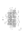
図2は、図1のメモリアレイMARYの一部を拡大した平面図である。なお、この平面図および以下の平面図では部材を構成するパターンの形状を示し、実際の部材の形状を表すものではない。つまり、図示するパターンは長方形あるいは正方形に描画されているが、実際の部材では頂角が丸くあるいは鈍角に形成さている。メモリアレイMARYには、活性領域L1が配置され、Y方向(第2方向)にワード線WLが、X方向(第1方向)にビット線BLが形成されている。ワード線WLと活性領域L1との重なる領域では、ワード線WLは、選択MISFETQsのゲート電極として機能する。ワード線WLのゲート電極として機能する領域に挟まれた活性領域L1の領域、つまり活性領域L1の中央部分にはビット線BLに接続する接続プラグBPが形成されている。接続プラグBPは活性領域L1とビット線BLにまたがるようにY方向に長い形状を有しており、活性領域L1の中央部分とビット線とは接続プラグBPを介して接続される。活性領域L1の両端領域は容量電極接続孔SNCTを介してキャパシタCに接続される。
【0030】
本実施の形態においては、ビット線BLと活性領域L1とは、X方向に延在した直線形状で形成されている。このように直線形状で形成されるため、ビット線BLおよび活性領域L1の加工の際のフォトリソグラフィにおいて露光光の干渉を少なくし、加工マージンを向上できる。
【0031】
図3は、本実施の形態のDRAMの一部断面図であり、(a)、(b)、(c)および(d)は、各々図2におけるC−C線断面、A−A線断面、D−D線断面およびB−B線断面を示す。なお、図3(a)においては、左方にDRAMのメモリセル領域を、右方に周辺回路領域を示している。また、本実施の形態では0.18μmの設計ルールでの製造技術を例示する。
【0032】
半導体基板1の主面には、メモリセル領域のp形ウェル2、周辺回路領域のp形ウェル3およびn形ウェル4が形成されている。半導体基板1は、たとえば10Ω・cmの抵抗率のp形の単結晶シリコンからなる。また、p形ウェル2の主面にはしきい値電圧調整層5が形成され、p形ウェル2を囲むようにn形のディープウェル6が形成されている。なお、他の各ウェルにも、しきい値電圧調整層が形成されていてもよい。
【0033】
各ウェルの主面には、分離領域7が形成されている。分離領域7はシリコン酸化膜からなり、半導体基板1の主面に形成された浅溝8に埋め込んで形成される。浅溝8は、たとえば0.3μmの深さを有し、内壁には熱酸化されたシリコン酸化膜が形成されてもよい。
【0034】
p形ウェル2の主面にはDRAMの選択MISFETQsが形成されている。また、p形ウェル3およびn形ウェル4の主面には各々nチャネルMISFETQnおよびpチャネルMISFETQpが形成されている。
【0035】
選択MISFETQsは、p形ウェル2の主面上にゲート絶縁膜10を介して形成されたゲート電極11と、ゲート電極11の両側のp形ウェル2の主面に形成された半導体領域12とを有する。
【0036】
ゲート絶縁膜10は、たとえば7〜8nmの膜厚を有する熱酸化により形成されたシリコン酸化膜からなる。
【0037】
ゲート電極11は、たとえば50nmの膜厚の多結晶シリコン膜と100nmの膜厚のタングステンシリサイド(WSi2 )膜との積層膜とすることができる。多結晶シリコン膜には、たとえばリン(P)を3×10²⁰atoms/cm3 程度導入することができる。なお、タングステンシリサイド膜に限られず、コバルトシリサイド(CoSi)膜、チタンシリサイド(TiSi)膜等の他のシリサイド膜であってもよい。また、ゲート電極11は、たとえば膜厚70nmの多結晶シリコン膜、膜厚50nmの窒化チタン膜および膜厚100nmのタングステン膜の積層膜とすることもできる。窒化チタン膜に代えて窒化タングステン膜を用いることもできる。
【0038】
半導体領域12にはn形の不純物、たとえば砒素(As)またはリンが導入されている。
【0039】
選択MISFETQsのゲート電極11の上層にはシリコン窒化膜からなるキャップ絶縁膜13が形成され、さらにその上層をシリコン窒化膜14で覆われる。キャップ絶縁膜13の膜厚はたとえば200nmであり、シリコン窒化膜14の膜厚はたとえば30nmである。シリコン窒化膜14は、ゲート電極11の側壁にも形成され、後に説明する接続孔を形成する際の自己整合加工に利用される。なお、選択MISFETQsのゲート電極11は、DRAMのワード線WLとして機能するものであり、分離領域7の上面にはワード線WLの一部が形成されている。
【0040】
一方、nチャネルMISFETQnおよびpチャネルMISFETQpは、各々p形ウェル3およびn形ウェル4の主面上に形成され、ゲート絶縁膜10を介して形成されたゲート電極11と、ゲート電極11の両側の各ウェルの主面に形成された半導体領域15とから構成される。ゲート絶縁膜10およびゲート電極11は前記と同様である。半導体領域15は低濃度不純物領域15aと高濃度不純物領域15bとからなり、いわゆるLDD(Lightly Doped Drain )構造を形成している。半導体領域15に導入される不純物は、MISFETの導電形に応じてn形またはp形の不純物が導入される。
【0041】
nチャネルMISFETQnおよびpチャネルMISFETQpのゲート電極11の上層にはシリコン窒化膜からなるキャップ絶縁膜13が形成され、さらにその上層およびゲート電極11とキャップ絶縁膜13との側壁がシリコン窒化膜14で覆われる。キャップ絶縁膜13とシリコン窒化膜14は前記と同様である。
【0042】
選択MISFETQs、nチャネルMISFETQnおよびpチャネルMISFETQpのゲート電極11間のギャップには、絶縁膜16が埋め込まれている。絶縁膜16は、たとえばSOG(Spin On Glass )膜、TEOS(テトラエトキシシラン)を原料ガスとしプラズマCVD法により形成されたシリコン酸化膜(以下TEOS酸化膜という)がCMP(Chemical Mechanical Polishing )法により平坦化されたTEOS酸化膜の積層膜とすることができる。
【0043】
絶縁膜16上には、絶縁膜17a、17b、17cが形成される。絶縁膜17a、17cは、たとえばTEOS酸化膜からなり、絶縁膜17bは、たとえばシリコン窒化膜からなる。絶縁膜17bは、後に説明するように、絶縁膜17cに配線溝をエッチングする際のエッチングストッパとして機能する。
【0044】
絶縁膜17b、17cには、配線溝18aが形成され、絶縁膜17aには、配線溝18bが形成されている。配線溝18a、18bの内部には、ビット線BLおよび第1層配線20が形成される。ビット線BLは、配線溝18bを介して、後に説明する接続プラグ21に電気的に接続される。
【0045】
ビット線BLおよび第1層配線20は後に説明するようにCMP法を用いて同時に形成される。ビット線BLおよび第1層配線20は、たとえばタングステン膜から構成されるが、他の金属、たとえば銅膜等を用いてもよい。
【0046】
ビット線BLは接続プラグ21を介して一対の選択MISFETQsに共有される半導体領域12に接続される。接続プラグ21は図2の平面図にも示されるように、活性領域L1のパターンとビット線BLのパターンに重なるようにY方向に長く形成される。
【0047】
また、選択MISFETQsの他方の半導体領域12上にはキャパシタに接続される接続プラグ22が形成されている。接続プラグ21、22は、n形の不純物たとえばリンが2×10²⁰atoms/cm3 程度導入された多結晶シリコン膜とする。
【0048】
なお、周辺回路領域(周辺回路領域)に形成されたnチャネルMISFETQnおよびpチャネルMISFETQpの高濃度不純物領域15bには第1層配線20(ビット線BL)が直接接続される。なお、高濃度不純物領域15bの表面にはコバルト、チタン、タンタル、タングステン等のシリサイド膜を形成できる。
【0049】
ビット線BLおよび第1層配線20は、層間絶縁膜23で覆われている。層間絶縁膜23は、たとえばTEOS酸化膜とすることができる。
【0050】
層間絶縁膜23の上層のメモリセル領域には、シリコン窒化膜からなる絶縁膜24が形成され、さらに情報蓄積用のキャパシタCが形成されている。絶縁膜24は後に説明するようにキャパシタCの下部電極27を形成する際のエッチングストッパとして機能する薄膜である。
【0051】
キャパシタCは、接続プラグ22に接続プラグ25を介して接続される下部電極27と、たとえばシリコン窒化膜および酸化タンタルからなる容量絶縁膜28と、たとえば窒化チタンからなるプレート電極29とから構成される。接続プラグ25は容量電極接続孔26内に形成される。
【0052】
キャパシタCの上層には、たとえばTEOS酸化膜からなる絶縁膜30が形成されている。なお、周辺回路領域の層間絶縁膜23の上層にはキャパシタCと同層に絶縁膜が形成されてもよい。この絶縁膜により、キャパシタCの標高に起因するメモリセル領域と周辺回路領域との間の段差の発生を防止することができ、フォトリソグラフィの焦点深度に余裕を持たせることができ、工程を安定にして微細加工に対応することができる。
【0053】
絶縁膜30の上層には第2層配線31が形成され、第2層配線31と上部電極29あるいは第1層配線20との間はプラグ32で接続される。第2層配線31は、たとえば窒化チタン膜、アルミニウム膜および窒化チタン膜の積層膜とすることができ、プラグ32は、たとえばチタン膜、窒化チタン膜およびタングステン膜の積層膜とすることができる。
【0054】
なお、第2層配線31上にはさらに層間絶縁膜を介して第3層配線あるいはそれ以上の配線層を有してもよいが、説明を省略する。
【0055】
次に、本実施の形態1のDRAMの製造方法を図面を用いて説明する。図4〜図19は本実施の形態1のDRAMの製造方法の一例を工程順に示した断面図または平面図である。なお、特に示さない限り断面図は図2におけるC−C線断面および周辺回路部分の断面を示す。
【0056】
まず、図4(a)に示すように、たとえば10Ω・cm程度の抵抗率を有するp形の半導体基板1を用意し、この半導体基板1の主面に深さがたとえば0.3μmの浅溝8を形成する。その後半導体基板1に熱酸化を施し、シリコン酸化膜を形成してもよい。さらにシリコン酸化膜を堆積してこれをCMP法により研磨して浅溝8内にのみシリコン酸化膜を残し、分離領域7を形成する。
【0057】
なお、このときの分離領域7で囲まれる活性領域L1のパターンは、図4(c)に示されるように、直線状の平面パターンである。このため、フォトリソグラフィによる浅溝8の加工において、露光光の干渉等の加工精度の低下要因を極力排除して、フォトリソグラフィの加工限界付近でも精度よく加工を行うことができる。
【0058】
次に、フォトレジストをマスクにしてリンイオンを注入してディープウェル6を形成し、その後フォトレジストをマスクにしてリンイオンをイオン注入しn形ウェル4を形成する。さらにフォトレジストをマスクにしてボロンイオンをイオン注入し、p形ウェル2、3を形成する。さらに半導体基板1の全面に二沸化ボロン(BF2 )イオンをイオン注入してもよい。
【0059】
次に、図4(b)に示すように、p形ウェル2、3、n形ウェル4が形成された活性領域に熱酸化法によりゲート絶縁膜10を形成し、さらに、DRAMのメモリセル領域に、加速エネルギ20keV、ドーズ量3×10¹²/cm2 程度の条件でボロンイオンをイオン注入し、選択MISFETQsのしきい値電圧調整層5を形成する。しきい値電圧調整層5により選択MISFETQsのしきい電圧を0.7V程度に調整できる。
【0060】
次に、半導体基板1の全面に、たとえば不純物としてリンが3×10²⁰/cm3 の濃度で導入された多結晶シリコン膜を50nmの膜厚で形成し、次に、たとえば100nmの膜厚でタングステンシリサイド膜を堆積する。さらにシリコン窒化膜をたとえば200nmの膜厚で堆積する。多結晶シリコン膜およびシリコン窒化膜は、たとえばCVD(Chemical Vapor Deposition )法により、タングステンシリサイド膜はスパッタ法により形成できる。その後、シリコン窒化膜、タングステンシリサイド膜および多結晶シリコン膜をフォトリソグラフィ技術およびエッチング技術を用いてパターニングし、ゲート電極11(ワード線WL)およびキャップ絶縁膜13を形成する。このときのワード線WL(キャップ絶縁膜13も同様である。)のパターンを図4(c)に示す。ワード線WLは、直線状にパターニングされており、フォトリソグラフィがその加工限界においても容易に行うことができることがわかる。
【0061】
次に、キャップ絶縁膜13およびゲート電極11とフォトレジストをマスクとして、メモリセル形成領域および周辺回路領域のnチャネルMISFETQnが形成される領域に不純物たとえばヒ素(As)またはリンをイオン注入し、半導体領域12およびnチャネルMISFETQnの低濃度不純物領域15aを形成する。その後、周辺回路領域のpチャネルMISFETQpが形成される領域に不純物たとえばボロン(B)をイオン注入し、pチャネルMISFETQpの低濃度不純物領域15aを形成する。
【0062】
次に、図5(a)に示すように、半導体基板1の全面にシリコン窒化膜14を、たとえば30nmの膜厚で堆積する。なお、メモリセル形成領域にのみ形成されたフォトレジスト膜をマスクとして、シリコン窒化膜14を異方性エッチングし、メモリセル領域の半導体基板1上にのみシリコン窒化膜14を残存させると同時に周辺回路領域のゲート電極11の側壁にサイドウォールスペーサを形成してもよい。
【0063】
次に、メモリセル形成領域と周辺回路領域のnチャネルMISFETQnが形成される領域とにフォトレジスト膜を形成し、このフォトレジスト膜とシリコン窒化膜14をマスクにして不純物たとえばボロンをイオン注入し、pチャネルMISFETQpの高濃度不純物領域15bを形成し、さらに、メモリセル形成領域と周辺回路領域のpチャネルMISFETQpが形成される領域とにフォトレジスト膜を形成し、このフォトレジスト膜とシリコン窒化膜14をマスクにして不純物たとえばリンをイオン注入し、nチャネルMISFETQnの高濃度不純物領域15bを形成する。
【0064】
次に、たとえば膜厚が400nmのシリコン酸化膜をCVD法により形成し、さらにこのシリコン酸化膜をCMP(Chemical Mechanical Polishing )法により研磨して平坦化し、絶縁膜16を形成する。
【0065】
この後、図5(b)に示すような接続プラグ21のパターンBPおよび接続プラグ22のパターンSNCTに相当する接続孔を開口し、プラグインプラを施した後に不純物がドープされた多結晶シリコン膜を堆積し、この多結晶シリコン膜をCMP法により研磨して接続プラグ21、22を形成する(図6)。なお、図6において、(a)、(b)、(c)および(d)は、各々図2におけるC−C線断面、A−A線断面、D−D線断面およびB−B線断面を示す。以下、図7、9、10、12、14〜19において同様である。
【0066】
プラグインプラは、たとえばリンイオンを加速エネルギ50keV、ドーズ量1×10¹³/cm2 とすることができる。また、多結晶シリコン膜への不純物の導入は、たとえばCVD法により濃度2×10²⁰/cm3 のリンを導入して行うことができる。なお、この接続孔は、2段階のエッチングにより開口して半導体基板1の過剰エッチングを防止することができる。また、接続プラグ21、22の形成はエッチバック法により形成することもできる。
【0067】
次に、配線形成用の絶縁膜17a、17b、17cを順次形成し、さらに、絶縁膜17c上にタングステン膜33を形成する(図7)。絶縁膜17a、17b、17cとしては、各々シリコン酸化膜、シリコン窒化膜およびシリコン酸化膜を適用できる。シリコン酸化膜およびシリコン窒化膜は、CVD法またはスパッタ法により形成できる。
【0068】
次に、タングステン膜33上にフォトレジスト膜34を形成する。フォトレジスト膜34は、図8および図9に示すようにビット線BLが形成される領域に開口を有するように形成される。すなわち、メモリセル形成領域では、フォトレジスト膜34は直線状に形成される。このため、微細なパターニングであっても露光光の回折等が発生し難く、高精度に露光を行うことができ、微細化に有利である。
【0069】
次に、フォトレジスト膜34をマスクとしてタングステン膜33をエッチングする(図9)。パターニングされたタングステン膜33は絶縁膜17cのエッチングの際のマスクに用いられる。また、後に説明するように、絶縁膜17aへの配線溝18bの形成の際のマスクの一部として機能する。
【0070】
次に、フォトレジスト膜34を除去した後、パターニングされたタングステン膜33をマスクとして絶縁膜17cおよび絶縁膜17bをエッチングし、絶縁膜17cに配線溝18aを形成する(図10)。
【0071】
配線溝18aの形成は、まず第1のエッチングとして、タングステン膜33をマスクとした絶縁膜17cのエッチングを行う。この第1のエッチングは、絶縁膜17c(たとえばシリコン酸化膜)のエッチング速度が高く、絶縁膜17b(たとえばシリコン窒化膜)のエッチング速度が低い条件で行う。つまり、第1のエッチングにおいて絶縁膜17b(たとえばシリコン窒化膜)は絶縁膜17c(たとえばシリコン酸化膜)のエッチングストッパとして機能する。このように絶縁膜17bを設けることにより、この第1のエッチングにおいて十分なオーバーエッチングが可能となる。エッチング工程における半導体ウェハ内のエッチング速度の不均一性は、エッチング深さのばらつきとして現れるが、この第1のエッチングにおいて仮にエッチング速度にウェハ内のばらつきが存在しても、十分なオーバーエッチングを行って絶縁膜17bをエッチングストッパとして作用させることにより、エッチング深さを均一にすることができる。次に、第2のエッチングとして絶縁膜17bをエッチングする。第2のエッチングは、絶縁膜17b(たとえばシリコン窒化膜)のエッチング速度が低い条件で行う。絶縁膜17bは、絶縁膜17cよりも薄く形成でき、このように薄く形成することにより、第2のエッチングの際のオーバーエッチングを行っても絶縁膜17bの膜厚が相対的に薄いゆえ下地である絶縁膜17aの過剰なエッチングを少なくできる。つまり、絶縁膜17c、17bのエッチングを2段階に分け、前記のような条件でエッチングを行うことにより、配線溝18aの深さを均一にし、かつ確実に配線溝18aの形成を行うことができる。
【0072】
次に、図11に示すように、フォトレジスト膜35を形成し、フォトレジスト膜35およびタングステン膜33の存在下で絶縁膜17aをエッチングする(図12)。これにより配線溝18bを形成する。フォトレジスト膜35は、図示するようにy方向(ワード線WLの延在方向)に並行に直線状に形成される。すなわち、フォトレジスト膜35は、活性領域L1の中央部分とビット線BLとを接続する接続プラグBP(プラグ21)が形成される領域が覆われないように、逆に活性領域L1の両端領域の容量電極接続孔SNCTを覆うようにストライプ状に形成される。
【0073】
一方、この段階ではタングステン膜33は依然として存在している。このため、タングステン膜33の形成されている領域の絶縁膜17a、17b、17cはフォトレジスト膜35が存在していなくてもエッチングされることはない。すなわち、絶縁膜17aのエッチングされる領域は、タングステン膜33が形成されておらず、かつ、フォトレジスト膜35で覆われていない領域となる。つまり、この段階でのエッチングは、フォトレジスト膜35で覆われていない配線溝18aの底部のみとなる。
【0074】
このように、フォトレジスト膜35とタングステン膜33とをマスクとしてエッチングすることにより、配線溝18bは、配線溝18aに対してy方向(ワード線WLの延在方向)に自己整合的に形成される。後に説明するように配線溝18aにはビット線BLが形成され、ビット線BLとプラグ21とは配線溝18bを介して接続されるため、配線溝18bはビット線接続孔として機能する。すなわち、ビット線接続孔として機能する配線溝18bをビット線BLに対して自己整合的に形成でき、ビット線BLとプラグ21との電気的接続を簡便にかつ高い信頼性で実現できる。
【0075】
また、ビット線接続孔を開口するためのマスクの精度を低減することもできる。すなわち、ビット線接続孔である配線溝18bのy方向のアライメントは配線溝18a(タングステン膜33)によってすでに自己整合されているため行う必要がなく、フォトレジスト膜35は、プラグ21上部が開口するようにパターニングすれば十分であり、その加工精度を高める必要はない。フォトレジスト膜35の開口幅(フォトレジスト膜35が形成されない領域の幅)はプラグ21の幅よりも大きく形成することができ、その幅のマージン分だけフォトレジスト膜35を形成するアライメントがx方向にずれてもよい。このようなずれが生じても配線溝18bを介してビット線BLがプラグ21に接続する限りDRAMの性能を阻害することはない。
【0076】
次に、図13に示すように、フォトレジスト膜36を形成し、周辺回路領域のMISFETのソース・ドレイン領域(高濃度不純物領域15b)に接続する接続孔を開口する。なお、この接続孔を開口する工程は、シリコン窒化膜14をストッパとする第1のエッチングとシリコン窒化膜14をエッチングする第2のエッチングの2段階のエッチングを行って、半導体基板1の表面の分離領域7の過剰なエッチングを防止することができる。この接続孔は、第1層配線20を直接高濃度不純物領域15bに接続するためのものであり、これにより周辺回路領域での配線抵抗を低減してDRAMの性能を向上できる。なお、この接続孔が形成される領域にはあらかじめ接続プラグを形成していてもよい。
【0077】
なお、絶縁膜17a、17b、17cの膜厚は、各々たとえば200nm、50nm、200nmとすることができる。また、配線溝18a、18bの深さは、各々たとえば250nm、200nmとすることができ、配線溝18aの幅は、180nmとすることができる。
【0078】
次に、たとえばスパッタ法により、膜厚が300nmのタングステン膜37を半導体基板1の全面に形成する(図14)。ここでは、タングステン膜37を例示しているが、他の金属膜、たとえば、銅膜等を用いてもよい。ただし、半導体基板1への金属原子の熱拡散による信頼性の低下を考慮すれば、金属膜は高融点金属であることが好ましい。たとえばモリブデン、タンタル、ニオブ等を例示できる。
【0079】
次に、タングステン膜37およびタングステン膜33を、たとえばCMP法により研磨し、配線溝18a以外のタングステン膜37を除去し、さらにタングステン膜33を除去することにより、ビット線BLおよび第1層配線20を形成する(図15)。なお、タングステン膜37の除去にはエッチバック法を用いることもできる。
【0080】
次に、半導体基板1の全面に、たとえばCVD法によりシリコン酸化膜を堆積し、このシリコン酸化膜をCMP法により研磨して平坦化し、層間絶縁膜23を形成する。その後半導体基板1の全面にシリコン窒化膜24および多結晶シリコン膜38を堆積する。多結晶シリコン膜38には、たとえば3×10²⁰/cm3 の濃度のリンを導入でき、その膜厚はたとえば100nmである。
【0081】
次に、図2に示すようなSNCTのパターンで、多結晶シリコン膜38に開口を形成する。開口の口径はたとえば0.22μmである。その後、半導体基板1の全面に多結晶シリコン膜38と同様の多結晶シリコン膜を膜厚70nmで堆積し、これを異方性エッチングして開口の側壁にサイドウォールスペーサ39を形成する。サイドウォールスペーサ39の幅は約70nmとなり、前記開口の口径はサイドウォールスペーサ39により80nmに縮小される。
【0082】
次に、多結晶シリコン膜38およびサイドウォールスペーサ39をハードマスクとしてエッチングを行い、容量電極接続孔26を形成する(図16)。容量電極接続孔26の口径は80nmであり、その深さは約300nmである。
【0083】
このように容量電極接続孔26の口径を小さく形成できるため、前記開口を形成するためのマスクに合わせずれが発生しても、ビット線BLと接触することがない。
【0084】
次に、容量電極接続孔26を埋め込む多結晶シリコン膜を堆積し、この多結晶シリコン膜、多結晶シリコン膜38およびサイドウォールスペーサ39をCMP法またはエッチバック法により除去して容量電極接続孔26の内部に接続プラグ25を形成する(図17)。接続プラグ25には、たとえば3×10²⁰/cm3 の濃度のリンを導入できる。なお、多結晶シリコン膜、多結晶シリコン膜38およびサイドウォールスペーサ39の除去の際には、シリコン窒化膜24をCMP法またはエッチバック法のエッチストッパ膜として機能させることができる。
【0085】
次に、たとえばCVD法によりシリコン酸化膜からなる絶縁膜40を堆積し、キャパシタCが形成される領域に溝41を形成する。絶縁膜40の堆積はプラズマCVDにより行うことができ、その膜厚はたとえば1.2μmとする。
【0086】
次に、溝41を覆う多結晶シリコン膜42を半導体基板1の全面に堆積し、さらに半導体基板1の全面にシリコン酸化膜43を堆積する(図18)。多結晶シリコン膜42にはリンをドープすることができ、その膜厚は0.03μmとすることができる。多結晶シリコン膜42の膜厚が溝41の寸法に対して十分に薄いため、多結晶シリコン膜42は溝41の内部にもステップカバレッジよく堆積される。シリコン酸化膜43は、溝41の内部に埋め込まれるように堆積する。溝41の内部への埋め込み性を考慮すれば、シリコン酸化膜43はSOG膜あるいはTEOSを用いたCVD法によるシリコン酸化膜とすることができる。
【0087】
次に、絶縁膜40上のシリコン酸化膜43および多結晶シリコン膜42を除去して、キャパシタCの下部電極27を形成する。シリコン酸化膜43および多結晶シリコン膜42の除去はエッチバック法またはCMP法により行うことができる。その後、ウェットエッチングを施し、下部電極27の内部に残存するシリコン酸化膜43および絶縁膜40を除去する。これにより下部電極27が露出される。なお、周辺回路領域にフォトレジスト膜を形成し、これをマスクとして周辺回路領域に絶縁膜40を残存させてもよい。なお、シリコン窒化膜24はこのウェットエッチング工程でのエッチングストッパとして機能する。
【0088】
次に、下部電極27表面を窒化または酸窒化処理した後、酸化タンタル膜を堆積し、容量絶縁膜28を形成する。酸化タンタル膜の堆積は、有機タンタルガスを原料としたCVD法により形成できる。この段階での酸化タンタル膜はアモルファス構造を有するものである。ここで酸化タンタル膜に熱処理を施して結晶化(多結晶化)された酸化タンタル膜(Ta2 O5 )とし、より強固な誘電体として容量絶縁膜28を形成してもよい。その後、プレート電極29となる窒化チタン膜をCVD法により堆積し、フォトレジスト膜を用いて前記窒化チタン膜および多結晶酸化タンタル膜をパターニングし、容量絶縁膜28およびプレート電極29を形成する。このようにして下部電極27、容量絶縁膜28およびプレート電極29からなるキャパシタCが形成される(図19)。なお、プレート電極29は、窒化チタン膜に代えて、たとえば4×10²⁰/cm3 の濃度のリンを含む多結晶シリコン膜としてもよい。
【0089】
その後、半導体基板1の全面に絶縁膜30を形成し、絶縁膜30に接続孔を形成し、その接続孔を含む絶縁膜30上に、たとえばチタン膜、窒化チタン膜およびタングステン膜を順次堆積し、これをCMP法またはエッチバック法により除去してプラグ32を形成し、この後、絶縁膜30上にたとえば窒化チタン膜、アルミニウム膜および窒化チタン膜からなる積層膜を堆積し、これをパターニングして第2層配線31を形成する。これにより図3に示すDRAMをほぼ完成する。さらに上層の配線層は第2層配線31と同様に形成できるため、その詳細な説明は省略する。
【0090】
本実施の形態のDRAMによれば、ビット線接続孔として機能する配線溝18bを、ビット線BLが形成される配線溝18aを形成するためのマスクとして機能するタングステン膜33およびy方向(ワード線WL方向)にストライプ状に形成されたフォトレジスト膜35をマスクとしてエッチングするため、ビット線BLに対して自己整合的に形成できる。これにより、ビット線BLとプラグ21との電気的接続を簡便にかつ高い信頼性で実現できる。
【0091】
なお、図20に示すように、絶縁膜16と絶縁膜17aとの間に、絶縁膜17aに対してエッチング選択比を有する絶縁膜44を形成することができる。図20(a)、(b)および(c)は、この場合を工程順に示した断面図であり、図20(a)は、図7(b)に、図20(c)は、図12(b)の工程に対応する。絶縁膜44としてはたとえばシリコン窒化膜を例示でき、膜厚はたとえば50nmである。
【0092】
このように絶縁膜44を設けることにより、配線溝18bの形成の際のエッチングを配線溝18aのエッチングと同様に2段階のエッチングで行うことができる。これにより、配線溝18bの過剰なエッチングを防止することができる。
【0093】
(実施の形態2)
図21〜図26は本実施の形態2のDRAMの製造方法の一例を工程順に示した断面図または平面図である。なお、図21、23、25、26において、(a)、(b)、(c)および(d)は、各々図2におけるC−C線断面、A−A線断面、D−D線断面およびB−B線断面を示す。
【0094】
本実施の形態のDRAMは、実施の形態1の場合とビット線BL(第1層配線20)の構造および製造方法において相違する。従って、その相違する部分についてのみ説明する。
【0095】
本実施の形態のDRAMの製造工程は、実施の形態1の図10の工程までは同様である。
【0096】
その後、半導体基板1の全面に、配線溝18aを埋め込むタングステン膜を堆積する。タングステン膜の膜厚は、配線溝18aの内部に被覆性よく堆積される程度とし、たとえば60nmとする。このタングステン膜を異方性エッチングすることにより、配線溝18aの内側壁にタングステンからなるサイドウォールスペーサ45を形成する(図21)。このときの配線溝18aおよびその内側壁に形成されたサイドウォールスペーサ45の平面パターンを図22に示す。サイドウォールスペーサ45に挟まれた領域には、次に説明するように配線溝18bが形成され、その幅は約60nmである。
【0097】
次に、タングステン膜33およびサイドウォールスペーサ45をマスクとして絶縁膜17aをエッチングし、配線溝18bを形成する(図23)。なお、このエッチングの際にはフォトレジスト膜は使用されない。すなわち、配線溝18bは、フォトレジスト膜を使用せずタングステン膜33およびサイドウォールスペーサ45をマスクとしてエッチングするため、配線溝18aと同様にx方向(ビット線BLが延在して形成される方向)に連続的に形成される。配線溝18bには後に説明するようにビット線BLの一部が形成され、プラグ21と電気的に接続されるが、このようにx方向に連続的に延在して形成されても、配線溝18bはプラグ22を露出することはない。すなわち、配線溝18bの幅はサイドウォールスペーサ45の形成により狭くなっている。このため、ビット線BLはプラグ22に接続されることはなく、プラグ22との絶縁性が保持される。
【0098】
また、配線溝18bに形成されるビット線BLの一部は、一種のビット線接続部と考えることもできる。すなわち、配線溝18bをビット線接続孔と考えることができる。このように考えた場合、ビット線接続孔は、配線溝18aすなわちビット線BLに対して自己整合的に形成され、実施の形態1と同様に微細加工が容易となる。
【0099】
また、本実施の形態では、フォトレジスト膜を使用することなく一種のビット線接続孔を形成でき、工程を簡略化することができる。
【0100】
次に、図24に示すように、フォトレジスト膜36を形成し、周辺回路領域のMISFETのソース・ドレイン領域(高濃度不純物領域15b)に接続する接続孔を開口する。この工程は、実施の形態1の図13の工程と同様である。
【0101】
次に、実施の形態1と同様に、たとえばスパッタ法により、膜厚が300nmのタングステン膜37を半導体基板1の全面に形成し(図25)、タングステン膜37およびタングステン膜33を、たとえばCMP法により研磨する(図26)。このとき、サイドウォールスペーサ45の上部も研磨され、その表面が平坦化される。これにより、サイドウォールスペーサ45およびタングステン膜37からなるビット線BLおよび第1層配線20を形成される。
【0102】
その後の工程は実施の形態1と同様である。
【0103】
本実施の形態のDRAMによれば、配線溝18aの内側壁にサイドウォールスペーサ45を形成し、これをマスクに用いて配線溝18bを形成するため、フォトレジスト膜を形成する必要がない。このため、配線溝18bを配線溝18aに対して自己整合的に形成でき、また、工程を簡略化できる。さらに、サイドウォールスペーサ45を配線(ビット線BL、第1層配線20)の一部として使用できるタングステンで構成するため、配線高さ(配線溝18aの深さ)を低減できる。これにより配線間容量を低減して蓄積電荷の検出感度の向上等DRAMの性能の向上を図れる。なお、配線溝18bの幅が狭いため、ビット線BLのプラグ21に接続する部分の幅が狭く形成される。このため、この配線幅の狭い領域での配線間容量の寄与を少なくできる。
【0104】
なお、本実施の形態では、配線溝18bの形成の際にフォトレジスト膜を形成しないことが特徴であるが、図27に示すようにフォトレジスト膜46を形成することもできる。フォトレジスト膜46は、実施の形態1のフォトレジスト膜35と同様に形成できる。この場合、図28に示すように、配線溝18bは、プラグ21の周辺領域に形成され、配線溝18aの延在方向に連続的に形成されることがない。このため、ビット線BLを形成した後には、図29に示すように、プラグ21上部に、配線溝18bに充填されたビット線BLの一部(プラグ接続部47)が形成され、その他のビット線延在方向には接続部は形成されない。このため、さらに配線間の容量を低減してDRAMの性能を向上できる。
【0105】
また、本実施の形態のように配線溝18aの内側壁にサイドウォールスペーサ45を形成する場合、周辺回路領域のコンタクト領域を図30に示すように広くすることができる。このように周辺回路領域のコンタクト領域を広くすることにより周辺回路領域でのコンタクト面積を確保してコンタクト抵抗を低減できる。
【0106】
また、実施の形態1と同様に、絶縁膜16と絶縁膜17aとの間に、絶縁膜17aに対してエッチング選択比を有する絶縁膜44を形成することができることは言うまでもない。
【0107】
(実施の形態3)
図31および図32は実施の形態3のDRAMの製造方法の一例を工程順に示した断面図である。なお、図31、32において、(a)、(b)および(c)、または、(d)、(e)および(f)は、各々図2におけるA−A線断面、D−D線断面およびB−B線断面を示す。
【0108】
本実施の形態のDRAMは、実施の形態1の場合とビット線BL(第1層配線20)の構造および製造方法において、また、ビット線BLが形成される絶縁膜の構造において相違する。従って、その相違する部分についてのみ説明する。
【0109】
本実施の形態のDRAMの製造工程は、実施の形態1の図9の工程までと同様である。ただし、本実施の形態では、配線溝が形成される絶縁膜48を、実施の形態1のように絶縁膜17a、17b、17cからなる3層膜とせず、単層膜としている。絶縁膜48はたとえばTEOS酸化膜とすることができる。
【0110】
実施の形態1の図9の工程のように、タングステン膜33をパターニングし、その後、パターニングされたタングステン膜33を覆うタングステン膜(図示せず)を堆積し、このタングステン膜を異方性エッチングすることにより、タングステン膜33の側壁にタングステンからなるサイドウォールスペーサ49を形成する(図31(a)、(b)および(c))。タングステン膜33のパターニングはフォトリソグラフィの最小加工寸法で行われるが、サイドウォールスペーサ49を形成することにより、最小加工寸法よりも小さなスペースを形成することができる。
【0111】
次に、タングステン膜33およびサイドウォールスペーサ49をマスクとして絶縁膜48をエッチングする。これにより、配線溝50を形成する(図31(d)、(e)および(f))。配線溝50は、前記の通りフォトリソグラフィの最小加工寸法以下の幅で形成される。
【0112】
なお、配線溝50の形成の際、実施の形態2と同様に、フォトレジスト膜は使用されない。これにより工程を簡略化することができる。
【0113】
また、配線溝50の底部においてプラグ21の表面が露出される。従って、後に説明するように、配線溝50の内部にビット線BLが形成されれば、ビット線自体がプラグ21と電気的に接続されることとなり、ビット線接続孔を形成する必要がない。すなわちビット線接続孔の形成を省略して、ビット線接続孔のパターニングに起因するプラグ21、ビット線BL間のマスクずれの問題を無くすことができる。
【0114】
次に、実施の形態1と同様に、周辺回路の接続孔を形成した後、たとえばスパッタ法により、膜厚が300nmのタングステン膜37を半導体基板1の全面に形成し(図32(a)、(b)および(c))、タングステン膜37、サイドウォールスペーサ49およびタングステン膜33を、たとえばCMP法により研磨する(図32(d)、(e)および(f))。これにより、ビット線BL(第1層配線20)が形成される。このようにして形成されたビット線BLの配線幅は、実施の形態1、2と比較して小さく形成される。これにより、配線間の距離を長くして配線間容量を低減できる。よって、蓄積電荷の検出感度を向上し、DRAMの性能を向上できる。
【0115】
その後の工程は実施の形態1と同様である。
【0116】
本実施の形態のDRAMによれば、フォトレジスト膜を用いることなく、ビット線接続孔の機能を併有する配線溝50を形成できる。これにより、工程を簡略化するとともに、ビット線接続孔の形成に起因するマスク合わせずれの問題を回避できる。また、ビット線BLの配線幅を狭く形成できるため、配線間距離を長くしてビット線間容量を低減し、蓄積電荷の検出感度向上等のDRAMの性能向上を図れる。
【0117】
なお、図33に示すように、タングステン膜33のパターニングの際に、下地である絶縁膜48を過剰にエッチングし、サイドウォールスペーサ49の底部をタングステン膜33の底面よりも低い標高で形成することができる(図33(a)、(b)および(c))。このようにして形成されたビット線BLには、その一部として絶縁膜48の表面付近にサイドウォールスペーサ49の一部を残存させることができる。このサイドウォールスペーサ49の一部によりビット線BLの断面積を増加させ、配線抵抗を低減してDRAMの高性能化に寄与できる。
【0118】
また、本実施の形態においても、実施の形態2と同様に、周辺回路領域のコンタクト領域を図30に示すように広くすることができ、実施の形態1と同様に、絶縁膜16と絶縁膜48との間に、絶縁膜48に対してエッチング選択比を有するシリコン窒化膜等を形成することができることは言うまでもない。
【0119】
以上、本発明者によってなされた発明を発明の実施の形態に基づき具体的に説明したが、本発明は前記実施の形態に限定されるものではなく、その要旨を逸脱しない範囲で種々変更可能であることは言うまでもない。
【0120】
たとえば、実施の形態1では、キャパシタCとして、上方に開口を有する筒形状の下部電極を有するキャパシタの例を示したが、単純スタック型のキャパシタを用いてもよい。
【0121】
また、本実施の形態のビット線BL(第1層配線20)の形成方法は、DRAMに限られず、DRAMを混載したロジック回路や、DRAMを混載したフラッシュメモリ内臓のマイクロコンピュータ、その他のシステム混載チップへの適用が可能である。
【0122】
また、本実施の形態のビット線BL(第1層配線20)の形成方法は、第1層の配線形成の適用に限られず、第2層以上の配線形成に適用することも可能である。この場合、図34に示すように、第N層配線51の形成後、第N層配線51を覆う絶縁膜52に第(N+1)層配線の接続孔53を開口する際に、第N層配線51に重なるように形成できる。これにより第N層配線51と第(N+1)層配線との電気的接続を容易に行うことができる。
【0123】
【発明の効果】
本願において開示される発明のうち、代表的なものによって得られる効果を簡単に説明すれば以下のとおりである。
【0124】
(1)微細化されたDRAMのメモリセルにおいて、ビット線と接続プラグとの電気的接続をワード線方向に自己整合で実現でき、ビット線と接続プラグとの電気的接続を簡便にかつ高い信頼性で実現できる。
【0125】
(2)ビット線と接続プラグとの接続部形成プロセスを簡略化することができる。
【0126】
(3)ビット線間の容量を低減し、蓄積電荷検出感度を向上してDRAMを高性能化できる。
【図面の簡単な説明】
【図1】(a)は、実施の形態1のDRAMを形成した半導体チップ全体の一例を示した平面図であり、(b)は、実施の形態1のDRAMの等価回路図である。
【図2】図1のメモリアレイMARYの一部を拡大した平面図である。
【図3】(a)〜(d)は、本発明の一実施の形態であるDRAMの一部断面図である。
【図4】(a)および(b)は、実施の形態1のDRAMの製造方法の一例を工程順に示した断面図であり、(c)は、平面図である。
【図5】(a)は、実施の形態1のDRAMの製造方法の一例を工程順に示した断面図であり、(b)は、平面図である。
【図6】(a)〜(d)は、実施の形態1のDRAMの製造方法の一例を工程順に示した断面図である。
【図7】(a)〜(d)は、実施の形態1のDRAMの製造方法の一例を工程順に示した断面図である。
【図8】実施の形態1のDRAMの製造方法の一例を工程順に示した平面図である。
【図9】(a)〜(d)は、実施の形態1のDRAMの製造方法の一例を工程順に示した断面図である。
【図10】(a)〜(d)は、実施の形態1のDRAMの製造方法の一例を工程順に示した断面図である。
【図11】実施の形態1のDRAMの製造方法の一例を工程順に示した平面図である。
【図12】(a)〜(d)は、実施の形態1のDRAMの製造方法の一例を工程順に示した断面図である。
【図13】実施の形態1のDRAMの製造方法の一例を工程順に示した断面図である。
【図14】(a)〜(d)は、実施の形態1のDRAMの製造方法の一例を工程順に示した断面図である。
【図15】(a)〜(d)は、実施の形態1のDRAMの製造方法の一例を工程順に示した断面図である。
【図16】(a)〜(d)は、実施の形態1のDRAMの製造方法の一例を工程順に示した断面図である。
【図17】(a)〜(d)は、実施の形態1のDRAMの製造方法の一例を工程順に示した断面図である。
【図18】(a)〜(d)は、実施の形態1のDRAMの製造方法の一例を工程順に示した断面図である。
【図19】(a)〜(d)は、実施の形態1のDRAMの製造方法の一例を工程順に示した断面図である。
【図20】(a)〜(c)は、実施の形態1のDRAMの製造方法の他の例を工程順に示した断面図である。
【図21】(a)〜(d)は、実施の形態2のDRAMの製造方法の一例を工程順に示した断面図である。
【図22】実施の形態2のDRAMの製造方法の一例を工程順に示した平面図である。
【図23】(a)〜(d)は、実施の形態2のDRAMの製造方法の一例を工程順に示した断面図である。
【図24】実施の形態2のDRAMの製造方法の一例を工程順に示した断面図である。
【図25】(a)〜(d)は、実施の形態2のDRAMの製造方法の一例を工程順に示した断面図である。
【図26】(a)〜(d)は、実施の形態2のDRAMの製造方法の一例を工程順に示した断面図である。
【図27】実施の形態2のDRAMの製造方法の他の例を工程順に示した平面図である。
【図28】(a)〜(d)は、実施の形態2のDRAMの製造方法の他の例を工程順に示した断面図である。
【図29】(a)〜(d)は、実施の形態2のDRAMの製造方法の他の例を工程順に示した断面図である。
【図30】実施の形態2のDRAMの製造方法のさらに他の例を示した平面図である。
【図31】(a)〜(f)は、実施の形態3のDRAMの製造方法の一例を工程順に示した断面図である。
【図32】(a)〜(f)は、実施の形態3のDRAMの製造方法の一例を工程順に示した断面図である。
【図33】(a)〜(f)は、実施の形態3のDRAMの製造方法の他の例を工程順に示した断面図である。
【図34】本発明の他の例を示した断面図である。
【符号の説明】
1 半導体基板
1A 半導体チップ
2 p形ウェル
3 p形ウェル
4 n形ウェル
5 しきい値電圧調整層
6 ディープウェル
7 分離領域
8 浅溝
10 ゲート絶縁膜
11 ゲート電極
11c 絶縁膜
12 半導体領域
13 キャップ絶縁膜
14 シリコン窒化膜
15 半導体領域
15a 低濃度不純物領域
15b 高濃度不純物領域
16 絶縁膜
17a 絶縁膜(TEOS酸化膜)
17b 絶縁膜(シリコン窒化膜)
17c 絶縁膜(TEOS酸化膜)
18a 配線溝
18b 配線溝
20 第1層配線
21 プラグ
22 プラグ
23 層間絶縁膜
24 絶縁膜(シリコン窒化膜)
25 接続プラグ
26 容量電極接続孔
27 下部電極
28 容量絶縁膜
29 プレート電極(上部電極)
30 絶縁膜
31 第2層配線
32 プラグ
33 タングステン膜
34 フォトレジスト膜
35 フォトレジスト膜
36 フォトレジスト膜
37 タングステン膜
38 多結晶シリコン膜
39 サイドウォールスペーサ
40 絶縁膜
41 溝
42 多結晶シリコン膜
43 シリコン酸化膜
44 絶縁膜
45 サイドウォールスペーサ
46 フォトレジスト膜
47 プラグ接続部
48 絶縁膜
49 サイドウォールスペーサ
50 配線溝
51 第N層配線
52 絶縁膜
53 接続孔
BL ビット線
BP 接続プラグ
C キャパシタ
L1 活性領域
MARY メモリアレイ
Qn nチャネルMISFET
Qp pチャネルMISFET
Qs 選択MISFET
SA センスアンプ
SNCT 容量電極接続孔
WD ワードドライバ
WL ワード線[0001]
BACKGROUND OF THE INVENTION
The present invention relates to a semiconductor device and a manufacturing technique thereof, and more particularly to a technique effective when applied to a random read / write memory (DRAM) that requires a memory holding operation suitable for high integration.
[0002]
[Prior art]
Generally, a trench type and a stacked type are known as the basic structure of a DRAM. The trench type is formed inside a trench in which an information storage capacitor (hereinafter simply referred to as a capacitor) is dug in a substrate, and the stacked type is a transfer transistor (hereinafter referred to as a selective MISFET (Metal Insulator Semiconductor) on the substrate surface. It is formed on top of the field effect transistor)). The stacked type is further classified into a CUB (Capacitor Under Bit-line) type in which a capacitor is disposed below the bit line and a COB (Capacitor Over Bit-line) type in which a capacitor is disposed above. In products of 64 Mbit or later, which have started mass production, the COB type is becoming the mainstream with a stacked type that has excellent cell area reduction.
[0003]
An example of the structure of a DRAM having COB type memory cells is as follows. That is, a DRAM memory cell having a COB type memory cell is arranged at the intersections of a plurality of word lines and a plurality of bit lines arranged in a matrix on the main surface of the semiconductor substrate, and one selection MISFET and This is composed of one capacitor connected in series. The selection MISFET is formed in an active region surrounded by an element isolation region, and is mainly composed of a gate oxide film, a gate electrode integrally formed with a word line, and a pair of semiconductor regions constituting a source and a drain. . The bit line is disposed above the selection MISFET and is electrically connected to one of the source and drain shared by two selection MISFETs adjacent in the extending direction. The capacitor is also disposed on the selection MISFET and is electrically connected to the other of the source and the drain. In order to compensate for the decrease in the accumulated charge amount (Cs) of the capacitor due to the miniaturization of the memory cell, the surface area of the capacitor disposed on the upper part of the bit line (storage electrode) is increased by processing it into a cylindrical shape, A capacitor insulating film and an upper electrode (plate electrode) are formed thereon. The structure of a COB type memory cell is described in, for example, Japanese Patent Application Laid-Open No. 7-7084, Japanese Patent Application No. 62-198043, Japanese Patent Application No. 63-10635, or Japanese Patent Application Laid-Open No. 8-167702. .
[0004]
In such a COB type memory cell structure, the bit line and the source / drain region of the selection MISFET are connected by a plug made of a polycrystalline silicon film or the like. In general, since a plug for capacitor connection is formed at the same time as a plug for bit line connection, at least one insulating film is provided between the plug and the bit line in order to insulate the bit line from the plug for capacitor connection. It is formed. Therefore, the bit line and the plug are connected via the bit line connection hole. In addition, a reduction in bit line capacitance is required from the viewpoint of improving the operation speed of DRAM and improvement in detection sensitivity of accumulated charges, and further, miniaturization of members such as bit lines is required from the viewpoint of realizing miniaturization. . In order to satisfy these requirements, for example, as described in International Publication WO98 / 28795, a bit line is formed by a damascene method, and a sidewall spacer made of a silicon nitride film is formed on the inner wall. It has been known. As a result, the bit lines are thinned, the distance between the bit lines is increased to reduce the capacity between the bit lines, and the speed of the DRAM and the sensitivity of detecting the storage capacity are improved.
[0005]
[Problems to be solved by the invention]
However, when the bit line is connected to the connection plug via the bit line connection hole, it is necessary to form the bit line pattern and the bit line connection hole pattern with different masks. Usually, after forming an isolation region on the main surface of a semiconductor substrate, a word line that also functions as a gate electrode of a MISFET is formed, and then a connection plug is formed. Further, when forming a bit line by the damascene method, after forming a groove of the bit line pattern, a bit line connection hole is formed, and a bit line connected to the connection plug is formed by a so-called dual damascene method. Here, the lithography for forming the connection plug is performed based on the word line pattern which is the gate electrode of the MISFET. However, since the connection plug for connecting the bit line and the connection plug for connecting the capacitor are generally formed in common, the bit line pattern and the bit line connection hole pattern to be formed next are photolithography based on the connection plug. In the same manner as the connection plug, photolithography is performed based on the word line pattern. That is, the bit line pattern and the bit line connection hole pattern are aligned between three layers, and pattern misalignment is likely to occur. In particular, misalignment between the bit line and the bit line connection hole does not cause much problem in the vertical direction of the word line because the bit line extends in the vertical direction of the word line, but is parallel to the word line. In such a direction, the size of misalignment directly affects the connection area, and there is a high risk of problems.
[0006]
Further, in the prior art, as a method of thinning the bit line, a sidewall spacer made of a silicon nitride film is formed on the inner wall of the groove formed in the bit line pattern, but the dielectric constant of the silicon nitride film is large, This increases the capacitance between the bit lines. An increase in bit line capacitance is undesirable because it causes a decrease in storage capacitor detection sensitivity and a decrease in DRAM operation speed.
[0007]
An object of the present invention is to provide a technology capable of realizing an electrical connection between a bit line and a connection plug in a word line direction in a miniaturized DRAM memory cell in a self-aligned manner, and an electrical connection between the bit line and the connection plug. The object is to provide a technology capable of easily and reliably realizing connection.
[0008]
Another object of the present invention is to simplify a process for forming a connection portion between a bit line and a connection plug.
[0009]
Another object of the present invention is to reduce the capacitance between bit lines.
[0010]
The above and other objects and novel features of the present invention will be apparent from the description of this specification and the accompanying drawings.
[0011]
[Means for Solving the Problems]
Of the inventions disclosed in the present application, the outline of typical ones will be briefly described as follows.
[0012]
(1) A manufacturing method of a semiconductor device of the present invention includes:A method of manufacturing a semiconductor device having a MISFET composed of a gate, a source and a drain on a semiconductor substrate,(A) On the main surface of the semiconductor substrateelementForming an isolation region,Surrounded by element isolation regionA step of arranging a plurality of active regions having long sides in a first direction; (b) a first layer extending on a main surface of a semiconductor substrate in a second direction perpendicular to the first direction and functioning as a gate electrode of a MISFET; A step of forming one wiring, (c) a step of forming a pair of semiconductor regions functioning as a source / drain of the MISFET in an active region between the first wirings, and (d) forming a first insulating film covering the first wiring. Forming a connection hole in the first insulating film on at least one semiconductor region of the semiconductor region, (e) forming a connection member electrically connected to the semiconductor region in the connection hole, and (f) connection Depositing a fourth insulating film having an etching selectivity with respect to the second insulating film, the third insulating film and the third insulating film on the member, and depositing a first film on the fourth insulating film; ) A first resist film extending in the first direction on the first film And turning, etching the first film in the presence of a first resist film in the presence of a first coat which is (h) etching the fourth insulating film by etching the third insulating film as a stopper film, furtherUntil the second insulating film is exposedEtching the third insulating film and extending in the first directionIn the third and fourth insulating filmsForming a first groove; (i) patterning a second resist film having an opening extending in the second direction; etching the second insulating film in the presence of the second resist film and the first film; Between the first coatingsEtch the second insulating film in the region where the second resist film does not existForming a second groove on the connecting member; (j) forming a first conductive film filling the first and second grooves on the entire surface of the semiconductor substrate; and (k) other than in the first and second grooves. Removing the first conductive film and forming a second wiring electrically connected to the connection member on one of the semiconductor regions in the first and second trenches.
[0013]
(2) A method for manufacturing a semiconductor device of the present invention includes: (a) a main surface of a semiconductor substrate;elementForming an isolation region,Surrounded by element isolation regionA step of arranging a plurality of active regions having long sides in a first direction; (b) a first layer extending on a main surface of a semiconductor substrate in a second direction perpendicular to the first direction and functioning as a gate electrode of a MISFET; A step of forming one wiring, (c) a step of forming a pair of semiconductor regions functioning as a source / drain of the MISFET in an active region between the first wirings, and (d) forming a first insulating film covering the first wiring. Forming a connection hole in the first insulating film on at least one semiconductor region of the semiconductor region, (e) forming a connection member electrically connected to the semiconductor region in the connection hole, and (f) connection Depositing a fourth insulating film having an etching selectivity with respect to the second insulating film, the third insulating film and the third insulating film on the member, and depositing a first film on the fourth insulating film; ) A first resist film extending in the first direction on the first film And turning, etching the first film in the presence of a first resist film in the presence of a first coat which is (h) etching, etching the fourth insulating film a third insulating film as a stopper, furtherUntil the second insulating film is exposedEtching the third insulating film and extending in the first directionIn the third and fourth insulating filmsForming a first groove; (i) forming a second conductive film covering the inner surface of the first groove on the entire surface of the semiconductor substrate; and subjecting the second conductive film to anisotropic etching to form an inner wall of the first groove (J) forming a second groove reaching the connecting member by etching the second insulating film in the presence of the first film and the sidewall; Forming a first conductive film for embedding the first and second grooves on the entire surface of the semiconductor substrate; (l) removing the first conductive film other than in the first and second grooves, and in the first and second grooves; And forming a second wiring electrically connected to the connection member on the one semiconductor region.
[0014]
(3) A method for manufacturing a semiconductor device according to the present invention is the method for manufacturing a semiconductor device according to (2), wherein the second resist film has an opening extending in the second direction before etching the second insulating film. Is patterned, and the second insulating film is etched in the presence of the second resist film, the first film, and the sidewall to form the second groove.
[0015]
(4) A method of manufacturing a semiconductor device according to the present invention includes: (a) a main surface of a semiconductor substrate;elementForming an isolation region,Surrounded by element isolation regionA step of arranging a plurality of active regions having long sides in a first direction; (b) a first layer extending on a main surface of a semiconductor substrate in a second direction perpendicular to the first direction and functioning as a gate electrode of a MISFET; A step of forming one wiring, (c) a step of forming a pair of semiconductor regions functioning as a source / drain of the MISFET in an active region between the first wirings, and (d) forming a first insulating film covering the first wiring. Forming a connection hole in the first insulating film on at least one semiconductor region of the semiconductor region, (e) forming a connection member electrically connected to the semiconductor region in the connection hole, and (f) connection Depositing a second insulating film on the member and depositing a first film on the second insulating film; (g) patterning the first resist film extending in the first direction on the first film; Etching the first film in the presence of the first resist film; h) A second conductive film is formed on the entire surface of the semiconductor substrate to cover the inner surface of the patterned first film, and anisotropic etching is performed on the second conductive film to form the second conductive film on the side wall of the first film. A step of forming a sidewall; (i) a step of etching the second insulating film in the presence of the first film and the sidewall to form a second groove reaching the connecting member; and (j) a second surface over the semiconductor substrate. (K) removing the first conductive film other than in the second groove, and electrically connecting to the connection member on one semiconductor region in the second groove. Forming a second wiring.
[0016]
(5) A method for manufacturing a semiconductor device according to the present invention is the method for manufacturing a semiconductor device according to (4), wherein the second insulating film that is the base of the first film is excessively etched in the etching process of the first film. Then, the bottom of the sidewall is formed deeper than the bottom of the first coating.
[0017]
(6) A method for manufacturing a semiconductor device according to the present invention is the method for manufacturing a semiconductor device according to any one of (1) to (5), wherein the first film and the first conductive film are made of the same material. In the first conductive film removal step, the first film, or the first film and the sidewall are removed together with the first conductive film.
[0018]
(7) A method of manufacturing a semiconductor device according to the present invention is the method of manufacturing a semiconductor device according to any one of (1) to (6), wherein a second insulating film and a connection member are formed on the top surface of the second insulating film. A fifth insulating film having an etching selectivity with respect to the insulating film is formed. In the second groove forming step, the fifth insulating film is used as a stopper.do itSecond insulating filmTheetchingdidAfter etching the fifth insulating filmTo form a second groove reaching the upper surface of the connection memberTo do.
[0019]
(8) Semiconductor device of the present inventionIs a method for manufacturing a semiconductor device according to any one of (1) to (6), wherein a sixth insulating film is formed on the second wiring, and a third insulating film is formed on the sixth insulating film. A conductive film is formed, a first opening is formed in the third conductive film by the third resist film, and then a fourth conductive film is formed on the entire surface and anisotropic etching is performed on the fourth conductive film. A sidewall is formed on the side wall of the one opening, and the sixth insulating film is etched using the third conductive film and the sidewall as a mask to form the second opening.Is.
[0020]
(9) Semiconductor device of the present inventionIs a method for manufacturing a semiconductor device according to (8), in which a fifth conductive film is formed on the entire surface so as to fill the second opening, and a third conductive film on the sixth insulating film and a sidewall are formed. Then, the fifth conductive film is removed by CMP to leave the fifth conductive film in the second opening to form a plug, and a capacitor is formed so as to be connected to the plug.Is.
[0021]
(10) A semiconductor device according to the present invention includes:An active region having a long side in the first direction by an isolation region formed on the main surface of the semiconductor substrate and a gate insulating film formed on the active region via a gate insulating film and extending in a second direction perpendicular to the first direction A gate electrode, a pair of semiconductor regions formed in active regions on both sides of the gate electrode, a connection plug formed in a first insulating film covering the gate electrode and connected to one semiconductor region of the pair of semiconductor regions; Second insulating film and third insulating film on the first insulating film, formed in the third insulating film, connected to the first groove extending in the first direction, and the connection plug, and formed in the second insulating film And a bit line formed so as to fill the groove formed of the second groove, a sidewall formed of a conductor is formed on the inner wall of the first groove, and the width of the second groove in the second direction Is narrower than the width of the first groove in the second direction by the thickness of the sidewall. , The second groove continuously in a first directionIs formed.
[0022]
(11) A semiconductor device according to the present invention includes:An active region having a long side in the first direction by an isolation region formed on the main surface of the semiconductor substrate and a gate insulating film formed on the active region via a gate insulating film and extending in a second direction perpendicular to the first direction A gate electrode, a pair of semiconductor regions formed in active regions on both sides of the gate electrode, a connection plug formed in a first insulating film covering the gate electrode and connected to one semiconductor region of the pair of semiconductor regions; Second insulating film and third insulating film on the first insulating film, formed in the third insulating film, connected to the first groove extending in the first direction, and the connection plug, and formed in the second insulating film And a bit line formed so as to fill the groove formed of the second groove, a sidewall formed of a conductor is formed on the inner wall of the first groove, and the width of the second groove in the second direction Is narrower than the width of the first groove by the thickness of the sidewall, and the second groove Formed discontinuously in the first direction, the second grooves only in a region which is connected to the connection plugIs formed.
[0023]
(12) A semiconductor device according to the present invention is the semiconductor device according to (11),The second groove is longer in the first direction than the diameter of the connection plug.Is formed.
[0024]
(13) A semiconductor device according to the present invention includes:(10), (11) or (12)The semiconductor device according to
[0025]
(14) The semiconductor device of the present invention is(13) In the semiconductor device according to (13), a second intermediate insulating film having an etching rate different from that of the second insulating film is provided between the second insulating film and the first insulating film.Is formed.
(15) A semiconductor device according to the present invention is the semiconductor device according to any one of (10) to (14), in which a first MISFET constituting a memory cell and a direct peripheral circuit are formed on a semiconductor substrate. The width of the bit line in the region connected to the source / drain region of the second MISFET is wider than the width of the bit line in the region connected to the source / drain region of the first MISFET. It is.
[0026]
DETAILED DESCRIPTION OF THE INVENTION
Hereinafter, embodiments of the present invention will be described in detail with reference to the drawings. Note that components having the same function are denoted by the same reference symbols throughout the drawings for describing the embodiments, and the repetitive description thereof will be omitted.
[0027]
(Embodiment 1)
FIG. 1A is a plan view showing an example of the entire semiconductor chip on which the DRAM of the first embodiment is formed. As shown in the figure, the main surface of the semiconductor chip 1A made of single crystal silicon has X direction (long side direction of the semiconductor chip 1A; first direction) and Y direction (short side direction of the semiconductor chip 1A; second direction). A large number of memory arrays MARY are arranged in a matrix. A sense amplifier SA is disposed between memory arrays MARY adjacent to each other along the X direction. In the central portion of the main surface of the semiconductor chip 1A, a control circuit such as a word driver WD and a data line selection circuit, an input / output circuit, a bonding pad, and the like are arranged.
[0028]
FIG. 1B is an equivalent circuit diagram of the DRAM of the first embodiment. As shown, the DRAM memory array (MARY) includes a plurality of word lines WL (WL) arranged in a matrix.0, WL1, WLn..) And a plurality of bit lines BL and a plurality of memory cells arranged at intersections thereof. One memory cell that stores 1-bit information includes one capacitor C and one selection MISFET Qs connected in series with the capacitor C. One of the source and the drain of the selection MISFET Qs is electrically connected to the capacitor C, and the other is electrically connected to the bit line BL. One end of the word line WL is connected to the word driver WD, and one end of the bit line BL is connected to the sense amplifier SA.
[0029]
FIG. 2 is an enlarged plan view of a part of the memory array MARY of FIG. In addition, this plan view and the following plan views show the shape of the pattern constituting the member, and do not represent the actual shape of the member. That is, although the pattern shown in the figure is drawn in a rectangle or a square, the apex angle is round or obtuse in an actual member. In the memory array MARY, an active region L1 is arranged, word lines WL are formed in the Y direction (second direction), and bit lines BL are formed in the X direction (first direction). In the region where the word line WL and the active region L1 overlap, the word line WL functions as a gate electrode of the selection MISFET Qs. A connection plug BP connected to the bit line BL is formed in a region of the active region L1 sandwiched between regions functioning as the gate electrode of the word line WL, that is, in the central portion of the active region L1. The connection plug BP has a long shape in the Y direction so as to straddle the active region L1 and the bit line BL, and the central portion of the active region L1 and the bit line are connected via the connection plug BP. Both end regions of the active region L1 are connected to the capacitor C through the capacitance electrode connection hole SNCT.
[0030]
In the present embodiment, the bit line BL and the active region L1 are formed in a linear shape extending in the X direction. Since it is formed in such a straight line shape, exposure light interference can be reduced and the processing margin can be improved in photolithography when processing the bit line BL and the active region L1.
[0031]
FIG. 3 is a partial cross-sectional view of the DRAM of the present embodiment. FIGS. , DD line cross section and BB line cross section are shown. In FIG. 3A, the DRAM memory cell region is shown on the left and the peripheral circuit region is shown on the right. In the present embodiment, a manufacturing technique with a design rule of 0.18 μm is illustrated.
[0032]
A p-type well 2 in the memory cell region, a p-
[0033]
An
[0034]
A DRAM selection MISFET Qs is formed on the main surface of the p-
[0035]
The selection MISFET Qs includes a
[0036]
The
[0037]
The
[0038]
An n-type impurity such as arsenic (As) or phosphorus is introduced into the
[0039]
A
[0040]
On the other hand, the n-channel MISFET Qn and the p-channel MISFET Qp are formed on the main surfaces of the p-
[0041]
A
[0042]
An insulating
[0043]
On the insulating
[0044]
A
[0045]
The bit line BL and the
[0046]
The bit line BL is connected to the
[0047]
Further, a
[0048]
The first layer wiring 20 (bit line BL) is directly connected to the high
[0049]
The bit line BL and the
[0050]
An insulating
[0051]
Capacitor C includes a
[0052]
Over the capacitor C, an insulating
[0053]
A
[0054]
The
[0055]
Next, a method for manufacturing the DRAM of the first embodiment will be described with reference to the drawings. 4 to 19 are sectional views or plan views showing an example of the manufacturing method of the DRAM according to the first embodiment in the order of steps. Unless otherwise indicated, the cross-sectional view shows a cross section taken along line CC in FIG. 2 and a cross section of a peripheral circuit portion.
[0056]
First, as shown in FIG. 4A, a p-
[0057]
Note that the pattern of the active region L1 surrounded by the
[0058]
Next, phosphorus ions are implanted using the photoresist as a mask to form the
[0059]
Next, as shown in FIG. 4B, a
[0060]
Next, for example, phosphorus as an impurity is 3 × 10 6 over the entire surface of the semiconductor substrate 1.20/ CmThreeA polycrystalline silicon film introduced at a concentration of 50 nm is formed to a thickness of 50 nm, and then a tungsten silicide film is deposited to a thickness of 100 nm, for example. Further, a silicon nitride film is deposited with a film thickness of 200 nm, for example. The polycrystalline silicon film and the silicon nitride film can be formed by, for example, CVD (Chemical Vapor Deposition), and the tungsten silicide film can be formed by sputtering. Thereafter, the silicon nitride film, the tungsten silicide film, and the polycrystalline silicon film are patterned using a photolithography technique and an etching technique to form the gate electrode 11 (word line WL) and the
[0061]
Next, using the
[0062]
Next, as shown in FIG. 5A, a
[0063]
Next, a photoresist film is formed in the memory cell formation region and the region where the n-channel MISFET Qn is formed in the peripheral circuit region, and impurities such as boron are ion-implanted using the photoresist film and the
[0064]
Next, for example, a silicon oxide film having a thickness of 400 nm is formed by a CVD method, and this silicon oxide film is polished and flattened by a CMP (Chemical Mechanical Polishing) method to form an insulating
[0065]
Thereafter, connection holes corresponding to the pattern BP of the
[0066]
The plug-in plastic, for example, uses phosphorus ions with an acceleration energy of 50 keV and a dose of 1 × 10.13/ Cm2It can be. Further, the introduction of impurities into the polycrystalline silicon film is performed at a concentration of 2 × 10 4 by, for example, the CVD method.20/ CmThreeThis can be done by introducing phosphorus. Note that this connection hole can be opened by two-stage etching to prevent excessive etching of the
[0067]
Next, insulating
[0068]
Next, a
[0069]
Next, the
[0070]
Next, after removing the
[0071]
The
[0072]
Next, as shown in FIG. 11, a
[0073]
On the other hand, the
[0074]
Thus, by etching using the
[0075]
In addition, the accuracy of the mask for opening the bit line connection hole can be reduced. That is, the alignment in the y direction of the
[0076]
Next, figure13As shown in FIG. 5, a
[0077]
Note that the film thicknesses of the insulating
[0078]
Next, a
[0079]
Next, the
[0080]
Next, a silicon oxide film is deposited on the entire surface of the
[0081]
Next, an opening is formed in the
[0082]
Next, etching is performed using the
[0083]
Thus, since the diameter of the capacitor
[0084]
Next, a polycrystalline silicon film filling the capacitive
[0085]
Next, an insulating
[0086]
Next, a
[0087]
Next, the
[0088]
Next, after nitriding or oxynitriding the surface of the
[0089]
Thereafter, an insulating
[0090]
According to the DRAM of the present embodiment, the
[0091]
As shown in FIG. 20, an insulating
[0092]
By providing the insulating
[0093]
(Embodiment 2)
FIG. 21 to FIG. 26 are cross-sectional views or plan views showing an example of the DRAM manufacturing method of the second embodiment in the order of steps. 21, 23, 25, and 26, (a), (b), (c), and (d) are the CC line cross section, the AA line cross section, and the DD line cross section in FIG. 2, respectively. And a cross section taken along line B-B.
[0094]
The DRAM of the present embodiment differs from that of the first embodiment in the structure of the bit line BL (first layer wiring 20) and the manufacturing method. Therefore, only the difference will be described.
[0095]
The manufacturing process of the DRAM of the present embodiment is the same up to the process of FIG. 10 of the first embodiment.
[0096]
Thereafter, a tungsten film for embedding the
[0097]
Next, the insulating
[0098]
In addition, a part of the bit line BL formed in the
[0099]
In this embodiment mode, a kind of bit line connection hole can be formed without using a photoresist film, and the process can be simplified.
[0100]
Next, as shown in FIG. 24, a
[0101]
Next, as in the first embodiment, a
[0102]
The subsequent steps are the same as those in the first embodiment.
[0103]
According to the DRAM of the present embodiment, the
[0104]
In this embodiment, the photoresist film is not formed when the
[0105]
When the
[0106]
Further, as in the first embodiment, it is needless to say that an insulating
[0107]
(Embodiment 3)
31 and 32 are cross-sectional views showing an example of a method of manufacturing the DRAM according to the third embodiment in the order of steps. 31 and 32, (a), (b) and (c), or (d), (e) and (f) are the AA line cross section and DD line cross section in FIG. 2, respectively. And a cross section taken along line B-B.
[0108]
The DRAM of the present embodiment differs from that of the first embodiment in the structure and manufacturing method of the bit line BL (first layer wiring 20) and in the structure of the insulating film in which the bit line BL is formed. Therefore, only the difference will be described.
[0109]
The manufacturing process of the DRAM of the present embodiment is the same as that up to the process of FIG. 9 of the first embodiment. However, in the present embodiment, the insulating
[0110]
As in the process of FIG. 9 of the first embodiment, the
[0111]
Next, the insulating
[0112]
In forming the
[0113]
Further, the surface of the
[0114]
Next, as in the first embodiment, after forming connection holes for peripheral circuits, a
[0115]
The subsequent steps are the same as those in the first embodiment.
[0116]
According to the DRAM of the present embodiment, the
[0117]
As shown in FIG. 33, when patterning the
[0118]
Also in the present embodiment, as in the second embodiment, the contact area in the peripheral circuit region can be widened as shown in FIG. 30, and as in the first embodiment, the insulating
[0119]
As mentioned above, the invention made by the present inventor has been specifically described based on the embodiments of the invention. However, the present invention is not limited to the above-described embodiments, and various modifications can be made without departing from the scope of the invention. Needless to say.
[0120]
For example, in the first embodiment, as the capacitor C, an example of a capacitor having a cylindrical lower electrode having an opening upward is shown, but a simple stack type capacitor may be used.
[0121]
In addition, the method of forming the bit line BL (first layer wiring 20) of the present embodiment is not limited to the DRAM, and a logic circuit in which DRAM is embedded, a microcomputer with built-in flash memory in which DRAM is embedded, and other system embedded. Application to chips is possible.
[0122]
In addition, the method of forming the bit line BL (first layer wiring 20) of the present embodiment is not limited to the application of the first layer wiring, but can be applied to the formation of the second layer or more. In this case, as shown in FIG. 34, after the Nth layer wiring 51 is formed, the Nth layer wiring is formed when the
[0123]
【The invention's effect】
Among the inventions disclosed in the present application, effects obtained by typical ones will be briefly described as follows.
[0124]
(1) In a miniaturized DRAM memory cell, the electrical connection between the bit line and the connection plug can be realized by self-alignment in the word line direction, and the electrical connection between the bit line and the connection plug is simple and highly reliable. It can be realized by sex.
[0125]
(2) A process for forming a connection portion between the bit line and the connection plug can be simplified.
[0126]
(3) The capacity between the bit lines can be reduced, the stored charge detection sensitivity can be improved, and the performance of the DRAM can be improved.
[Brief description of the drawings]
FIG. 1A is a plan view showing an example of an entire semiconductor chip on which a DRAM according to a first embodiment is formed, and FIG. 1B is an equivalent circuit diagram of the DRAM according to the first embodiment;
2 is an enlarged plan view of a part of the memory array MARY of FIG. 1;
FIGS. 3A to 3D are partial cross-sectional views of a DRAM according to an embodiment of the present invention.
4A and 4B are cross-sectional views showing an example of a method of manufacturing the DRAM of the first embodiment in the order of steps, and FIG. 4C is a plan view.
5A is a cross-sectional view showing an example of the manufacturing method of the DRAM of the first embodiment in the order of steps, and FIG. 5B is a plan view.
6A to 6D are cross-sectional views showing an example of a method of manufacturing the DRAM according to the first embodiment in the order of steps.
7A to 7D are cross-sectional views showing an example of a method for manufacturing the DRAM of the first embodiment in the order of steps.
FIG. 8 is a plan view showing an example of the manufacturing method of the DRAM according to the first embodiment in the order of steps.
9A to 9D are cross-sectional views showing an example of a method for manufacturing the DRAM of the first embodiment in the order of steps.
10A to 10D are cross-sectional views showing an example of a method for manufacturing the DRAM of the first embodiment in the order of steps.
FIG. 11 is a plan view showing an example of the manufacturing method of the DRAM according to the first embodiment in the order of steps.
12A to 12D are cross-sectional views showing an example of a method of manufacturing the DRAM of the first embodiment in the order of steps.
13 is a cross-sectional view showing an example of the manufacturing method of the DRAM of
14A to 14D are cross-sectional views showing an example of a method of manufacturing the DRAM of the first embodiment in the order of steps.
15A to 15D are cross-sectional views showing an example of a method for manufacturing the DRAM of the first embodiment in the order of steps.
16A to 16D are cross-sectional views showing an example of a method for manufacturing the DRAM of the first embodiment in the order of steps.
17A to 17D are cross-sectional views showing an example of a method for manufacturing the DRAM of the first embodiment in the order of steps.
18A to 18D are cross-sectional views showing an example of a method for manufacturing the DRAM of the first embodiment in the order of steps.
FIGS. 19A to 19D are cross-sectional views showing an example of a method for manufacturing the DRAM of the first embodiment in the order of steps; FIGS.
20A to 20C are cross-sectional views showing another example of the method for manufacturing the DRAM of the first embodiment in the order of steps.
FIGS. 21A to 21D are cross-sectional views showing an example of a method of manufacturing the DRAM of the second embodiment in the order of steps. FIGS.
FIG. 22 is a plan view showing one example of a method for manufacturing the DRAM of the second embodiment in the order of steps.
23A to 23D are cross-sectional views showing an example of a method for manufacturing the DRAM of the second embodiment in the order of steps.
24 is a cross-sectional view showing an example of the manufacturing method of the DRAM of
FIGS. 25A to 25D are cross-sectional views showing an example of a method of manufacturing the DRAM of the second embodiment in the order of steps. FIGS.
FIGS. 26A to 26D are cross-sectional views showing an example of a method of manufacturing the DRAM of the second embodiment in the order of steps. FIGS.
FIG. 27 is a plan view showing another example of the method for manufacturing the DRAM of the second embodiment in the order of steps.
FIGS. 28A to 28D are cross-sectional views showing another example of the DRAM manufacturing method of the second embodiment in the order of steps;
FIGS. 29A to 29D are cross-sectional views showing other examples of the method of manufacturing the DRAM of the second embodiment in the order of steps. FIGS.
30 is a plan view showing still another example of the method for manufacturing the DRAM of the second embodiment. FIG.
FIGS. 31A to 31F are cross-sectional views showing an example of a method of manufacturing the DRAM of the third embodiment in the order of steps. FIGS.
32 (a) to (f) are cross-sectional views showing an example of a method of manufacturing a DRAM of the third embodiment in the order of steps.
FIGS. 33A to 33F are cross-sectional views showing another example of the DRAM manufacturing method according to the third embodiment in the order of steps;
FIG. 34 is a cross-sectional view showing another example of the present invention.
[Explanation of symbols]
1 Semiconductor substrate
1A Semiconductor chip
2 p-type well
3 p-type well
4 n-type well
5 Threshold voltage adjustment layer
6 Deep Well
7 Separation area
8 shallow groove
10 Gate insulation film
11 Gate electrode
11c Insulating film
12 Semiconductor region
13 Cap insulation film
14 Silicon nitride film
15 Semiconductor region
15a Low concentration impurity region
15b High concentration impurity region
16 Insulating film
17a Insulating film (TEOS oxide film)
17b Insulating film (silicon nitride film)
17c Insulating film (TEOS oxide film)
18a Wiring groove
18b Wiring groove
20 First layer wiring
21 plug
22 plug
23 Interlayer insulation film
24 Insulating film (silicon nitride film)
25 connection plug
26 Capacitance electrode connection hole
27 Lower electrode
28 capacitive insulating film
29 Plate electrode (upper electrode)
30 Insulating film
31 Second layer wiring
32 plugs
33 Tungsten film
34 Photoresist film
35 Photoresist film
36 Photoresist film
37 Tungsten film
38 Polycrystalline silicon film
39 Sidewall spacer
40 Insulating film
41 groove
42 Polycrystalline silicon film
43 Silicon oxide film
44 Insulating film
45 Sidewall spacer
46 Photoresist film
47 Plug connection
48 Insulating film
49 Sidewall spacer
50 Wiring groove
51 Nth layer wiring
52 Insulating film
53 Connection hole
BL bit line
BP connection plug
C capacitor
L1 active region
MARY memory array
Qn n-channel MISFET
Qp p channel MISFET
Qs selection MISFET
SA sense amplifier
SNCT Capacitance electrode connection hole
WD Word driver
WL Word line
Claims (15)
(a)前記半導体基板の主面上に素子分離領域を形成し、前記素子分離領域に囲まれた第1方向に長辺を有する活性領域を複数配列する工程、
(b)前記半導体基板の主面上に、前記第1方向に垂直な第2方向に延在して、前記MISFETのゲート電極として機能する第1配線を形成する工程、
(c)前記第1配線間の前記活性領域に、前記MISFETのソース・ドレインとして機能する一対の半導体領域を形成する工程、
(d)前記第1配線を覆う第1絶縁膜を形成し、前記半導体領域の少なくとも一方の半導体領域上の前記第1絶縁膜に接続孔を形成する工程、
(e)前記接続孔内に前記半導体領域に電気的に接続する接続部材を形成する工程、
(f)前記接続部材上に、第2絶縁膜、第3絶縁膜および前記第3絶縁膜に対してエッチング選択比を有する第4絶縁膜を堆積し、前記第4絶縁膜上に第1被膜を堆積する工程、
(g)前記第1被膜上に前記第1方向に延在して第1レジスト膜をパターニングし、前記第1レジスト膜の存在下で前記第1被膜をエッチングする工程、
(h)前記エッチングされた第1被膜の存在下で、前記第3絶縁膜をストッパ膜として前記第4絶縁膜をエッチングし、さらに前記第2絶縁膜を露出するまで前記第3絶縁膜をエッチングし、前記第1方向に延在する前記第3および第4絶縁膜内に第1溝を形成する工程、
(i)前記第2方向に延在する開口を有する第2レジスト膜をパターニングし、前記第2レジスト膜および前記第1被膜の存在下で前記第2絶縁膜をエッチングし、前記エッチングされた第1被膜間で前記第2レジスト膜が存在しない領域の前記第2絶縁膜をエッチングして前記接続部材上に第2溝を形成する工程、
(j)前記半導体基板の全面に、前記第1および第2溝を埋め込む第1導電膜を形成する工程、
(k)前記第1および第2溝内以外の前記第1導電膜を除去し、前記第1および第2溝内に、前記一方の半導体領域上の前記接続部材に電気的に接続された第2配線を形成する工程、
を有することを特徴とする半導体装置の製造方法。 A method of manufacturing a semiconductor device having a MISFET composed of a gate, a source and a drain on a semiconductor substrate,
(A) step of the forming an isolation region in the semiconductor substrate on the principal surface, arranging a plurality of active regions having a long side in a first direction, surrounded by the element isolation region,
(B) the semiconductor substrate on the principal surface, extending in a second direction perpendicular to the first direction, forming a first wiring which functions as a gate electrode of the MISFET,
(C) forming a pair of semiconductor regions functioning as a source / drain of the MISFET in the active region between the first wirings;
(D) forming a first insulating film covering the first wiring and forming a connection hole in the first insulating film on at least one semiconductor region of the semiconductor region;
(E) forming a connection member electrically connected to the semiconductor region in the connection hole;
(F) depositing a second insulating film, a third insulating film, and a fourth insulating film having an etching selectivity with respect to the third insulating film on the connecting member, and forming a first coating on the fourth insulating film; Depositing,
(G) a step of patterning a first resist film extending in the first direction on the first film and etching the first film in the presence of the first resist film;
(H) In the presence of the etched first film, the fourth insulating film is etched using the third insulating film as a stopper film , and the third insulating film is etched until the second insulating film is exposed. And forming a first groove in the third and fourth insulating films extending in the first direction,
(I) patterning a second resist film having an opening extending in the second direction, etching the second insulating film in the presence of the second resist film and the first film, and Etching the second insulating film in a region where the second resist film does not exist between one film to form a second groove on the connection member;
(J) forming a first conductive film filling the first and second grooves on the entire surface of the semiconductor substrate;
(K) The first conductive film other than in the first and second grooves is removed, and the first conductive film is electrically connected to the connection member on the one semiconductor region in the first and second grooves. A step of forming two wirings;
A method for manufacturing a semiconductor device, comprising:
(b)前記半導体基板の主面上に、前記第1方向に垂直な第2方向に延在して、MISFETのゲート電極として機能する第1配線を形成する工程、
(c)前記第1配線間の前記活性領域に、前記MISFETのソース・ドレインとして機能する一対の半導体領域を形成する工程、
(d)前記第1配線を覆う第1絶縁膜を形成し、前記半導体領域の少なくとも一方の半導体領域上の前記第1絶縁膜に接続孔を形成する工程、
(e)前記接続孔内に前記半導体領域に電気的に接続する接続部材を形成する工程、
(f)前記接続部材上に、第2絶縁膜、第3絶縁膜および前記第3絶縁膜に対してエッチング選択比を有する第4絶縁膜を堆積し、前記第4絶縁膜上に第1被膜を堆積する工程、
(g)前記第1被膜上に前記第1方向に延在して第1レジスト膜をパターニングし、前記第1レジスト膜の存在下で前記第1被膜をエッチングする工程、
(h)前記エッチングされた第1被膜の存在下で、前記第3絶縁膜をストッパとして前記第4絶縁膜をエッチングし、さらに前記第2絶縁膜を露出するまで前記第3絶縁膜をエッチングし、前記第1方向に延在する前記第3および第4絶縁膜内に第1溝を形成する工程、
(i)前記半導体基板の全面に、前記第1溝の内面を覆う第2導電膜を形成し、前記第2導電膜に異方性エッチングを施して前記第1溝の内側壁に前記第2導電膜からなるサイドウォールを形成する工程、
(j)前記第1被膜およびサイドウォールの存在下で前記第2絶縁膜をエッチングし、前記接続部材に達する第2溝を形成する工程、
(k)前記半導体基板の全面に、前記第1および第2溝を埋め込む第1導電膜を形成する工程、
(l)前記第1および第2溝内以外の前記第1導電膜を除去し、前記第1および第2溝内に、前記一方の半導体領域上の前記接続部材に電気的に接続された第2配線を形成する工程、
を有することを特徴とする半導体装置の製造方法。(A) forming an element isolation region on a main surface of a semiconductor substrate and arranging a plurality of active regions having long sides in a first direction surrounded by the element isolation region ;
(B) forming on the main surface of the semiconductor substrate a first wiring extending in a second direction perpendicular to the first direction and functioning as a gate electrode of a MISFET;
(C) forming a pair of semiconductor regions functioning as a source / drain of the MISFET in the active region between the first wirings;
(D) forming a first insulating film covering the first wiring and forming a connection hole in the first insulating film on at least one semiconductor region of the semiconductor region;
(E) forming a connection member electrically connected to the semiconductor region in the connection hole;
(F) depositing a second insulating film, a third insulating film, and a fourth insulating film having an etching selectivity with respect to the third insulating film on the connecting member, and forming a first coating on the fourth insulating film; Depositing,
(G) a step of patterning a first resist film extending in the first direction on the first film and etching the first film in the presence of the first resist film;
(H) In the presence of the etched first film, the fourth insulating film is etched using the third insulating film as a stopper, and further, the third insulating film is etched until the second insulating film is exposed. Forming a first groove in the third and fourth insulating films extending in the first direction;
(I) forming a second conductive film covering the inner surface of the first groove on the entire surface of the semiconductor substrate, performing anisotropic etching on the second conductive film, and forming the second conductive film on the inner wall of the first groove; Forming a sidewall made of a conductive film;
(J) etching the second insulating film in the presence of the first coating and the sidewall to form a second groove reaching the connection member;
(K) forming a first conductive film filling the first and second grooves on the entire surface of the semiconductor substrate;
(L) The first conductive film other than in the first and second grooves is removed, and the first conductive film is electrically connected to the connection member on the one semiconductor region in the first and second grooves. A step of forming two wirings;
A method for manufacturing a semiconductor device, comprising:
前記第2絶縁膜のエッチング前に、前記第2方向に延在する開口を有する第2レジスト膜をパターニングし、前記第2レジスト膜、第1被膜およびサイドウォールの存在下で、前記第2絶縁膜をエッチングし、前記第2溝を形成することを特徴とする半導体装置の製造方法。A method of manufacturing a semiconductor device according to claim 2,
Before etching the second insulating film, a second resist film having an opening extending in the second direction is patterned, and the second insulating film is formed in the presence of the second resist film, the first film, and the sidewall. A method of manufacturing a semiconductor device, comprising etching the film to form the second groove.
(b)前記半導体基板の主面上に、前記第1方向に垂直な第2方向に延在して、MISFETのゲート電極として機能する第1配線を形成する工程、
(c)前記第1配線間の前記活性領域に、前記MISFETのソース・ドレインとして機能する一対の半導体領域を形成する工程、
(d)前記第1配線を覆う第1絶縁膜を形成し、前記半導体領域の少なくとも一方の半導体領域上の前記第1絶縁膜に接続孔を形成する工程、
(e)前記接続孔内に前記半導体領域に電気的に接続する接続部材を形成する工程、
(f)前記接続部材上に、第2絶縁膜を堆積し、前記第2絶縁膜上に第1被膜を堆積する工程、
(g)前記第1被膜上に前記第1方向に延在して第1レジスト膜をパターニングし、前記第1レジスト膜の存在下で前記第1被膜をエッチングする工程、
(h)前記半導体基板の全面に、前記パターニングされた第1被膜の内面を覆う第2導電膜を形成し、前記第2導電膜に異方性エッチングを施して前記第1被膜の側壁に前記第2導電膜からなるサイドウォールを形成する工程、
(i)前記第1被膜およびサイドウォールの存在下で前記第2絶縁膜をエッチングし、前記接続部材に達する第2溝を形成する工程、
(j)前記半導体基板の全面に、前記第2溝を埋め込む第1導電膜を形成する工程、
(k)前記第2溝内以外の前記第1導電膜を除去し、前記第2溝内に、前記一方の半導体領域上の前記接続部材に電気的に接続された第2配線を形成する工程、
を有することを特徴とする半導体装置の製造方法。(A) forming an element isolation region on a main surface of a semiconductor substrate and arranging a plurality of active regions having long sides in a first direction surrounded by the element isolation region ;
(B) forming on the main surface of the semiconductor substrate a first wiring extending in a second direction perpendicular to the first direction and functioning as a gate electrode of a MISFET;
(C) forming a pair of semiconductor regions functioning as a source / drain of the MISFET in the active region between the first wirings;
(D) forming a first insulating film covering the first wiring and forming a connection hole in the first insulating film on at least one semiconductor region of the semiconductor region;
(E) forming a connection member electrically connected to the semiconductor region in the connection hole;
(F) depositing a second insulating film on the connection member and depositing a first film on the second insulating film;
(G) a step of patterning a first resist film extending in the first direction on the first film and etching the first film in the presence of the first resist film;
(H) A second conductive film is formed on the entire surface of the semiconductor substrate to cover the inner surface of the patterned first film, and anisotropic etching is performed on the second conductive film to form the second conductive film on the side wall of the first film. Forming a sidewall made of the second conductive film;
(I) a step of etching the second insulating film in the presence of the first film and the sidewall to form a second groove reaching the connection member;
(J) forming a first conductive film filling the second groove on the entire surface of the semiconductor substrate;
(K) removing the first conductive film other than in the second groove and forming a second wiring electrically connected to the connection member on the one semiconductor region in the second groove. ,
A method for manufacturing a semiconductor device, comprising:
前記第1被膜のエッチング工程において、前記第1被膜の下地である前記第2絶縁膜を過剰にエッチングし、前記サイドウォールの底部を前記第1被膜の底部よりも深く形成することを特徴とする半導体装置の製造方法。A method of manufacturing a semiconductor device according to claim 4,
In the etching process of the first film, the second insulating film, which is a base of the first film, is excessively etched to form a bottom portion of the sidewall deeper than a bottom portion of the first film. A method for manufacturing a semiconductor device.
前記第1被膜と前記第1導電膜とは同一の材料からなり、前記第1導電膜の除去工程において、前記第1導電膜とともに、前記第1被膜、または、前記第1被膜およびサイドウォールを除去することを特徴とする半導体装置の製造方法。A method for manufacturing a semiconductor device according to any one of claims 1 to 5,
The first film and the first conductive film are made of the same material, and in the first conductive film removal step, the first film or the first film and the sidewall are formed together with the first conductive film. A method for manufacturing a semiconductor device, comprising: removing the semiconductor device.
前記第1絶縁膜および接続部材の上面に、前記第2絶縁膜に対してエッチング選択比を有する第5絶縁膜を形成し、前記第2溝の形成工程において、前記第5絶縁膜をストッパとして前記第2絶縁膜をエッチングした後、前記第5絶縁膜をエッチングして前記接続部材上面に達する前記第2溝を形成することを特徴とする半導体装置の製造方法。A method for manufacturing a semiconductor device according to any one of claims 1 to 6,
A fifth insulating film having an etching selectivity with respect to the second insulating film is formed on the top surfaces of the first insulating film and the connection member, and the fifth insulating film serves as a stopper in the step of forming the second groove. after etching the second insulating film and method of manufacturing a semiconductor device characterized by forming the second grooves reaching said connecting member upper surface by etching the fifth insulation film.
前記第2配線上に第6絶縁膜を形成し、前記第6絶縁膜上に第3導電膜を形成し、第3レジスト膜により前記第3導電膜に第1開口部を形成し、その後、第4導電膜を全面に形成して前記第4導電膜を異方性エッチングすることにより、前記第1開口部側壁にサイドウォールを形成し、前記第3導電膜およびサイドウォールをマスクとして前記第6絶縁膜をエッチングして第2開口部を形成することを特徴とする半導体装置の製造方法。Forming a sixth insulating film on the second wiring; forming a third conductive film on the sixth insulating film; forming a first opening in the third conductive film with a third resist film; A fourth conductive film is formed on the entire surface, and the fourth conductive film is anisotropically etched to form a sidewall on the side wall of the first opening, and the third conductive film and the sidewall are used as a mask to form the first conductive film. 6. A method of manufacturing a semiconductor device, wherein the second opening is formed by etching the insulating film.
前記第2開口部内を埋め込むように全面に第5導電膜を形成し、前記第6絶縁膜上の前記第3導電膜、前記サイドウォールおよび第5導電膜をCMP法により除去して前記第2開口部内に前記第5導電膜を残してプラグを形成し、前記プラグに接続するようにキャパシタを形成することを特徴とする半導体装置の製造方法。A fifth conductive film is formed on the entire surface so as to fill the second opening, and the third conductive film, the sidewalls, and the fifth conductive film on the sixth insulating film are removed by a CMP method to remove the second conductive film. A method of manufacturing a semiconductor device, comprising: forming a plug while leaving the fifth conductive film in an opening; and forming a capacitor so as to be connected to the plug.
前記第1溝の内側壁には導電体からなるサイドウォールが形成され、前記第2溝の前記第2方向の幅が前記サイドウォールの膜厚分だけ前記第1溝の前記第2方向の幅よりも狭くなっており、前記第2溝が前記第1方向に連続して形成されていることを特徴とする半導体装置。 An active area having a long side in the first direction by the isolation region formed on the main surface of the semiconductor substrate, is formed through a gate insulating film on the active region, in a second direction perpendicular to the first direction An extending gate electrode, a pair of semiconductor regions formed in the active region on both sides of the gate electrode, and a first insulating film covering the gate electrode, and formed in one semiconductor region of the pair of semiconductor regions A connected connection plug; a second insulating film and a third insulating film on the first insulating film; a first groove formed in the third insulating film and extending in the first direction; and the connecting plug A bit line formed so as to fill a groove formed of a second groove formed in the second insulating film .
The inner wall of the front Symbol first groove is formed sidewalls made of a conductive material, wherein the second width of the second groove is in the second direction of the film by a thickness worth the first groove of the side wall The semiconductor device is narrower than a width, and the second groove is formed continuously in the first direction.
前記第1溝の内側壁には導電体からなるサイドウォールが形成され、前記第2溝の前記第2方向の幅が前記サイドウォールの膜厚分だけ前記第1溝の幅よりも狭くなっており、前記第2溝が前記第1方向に不連続に形成され、前記第2溝は前記接続プラグに接続される領域にのみ形成されていることを特徴とする半導体装置。 An active area having a long side in the first direction by the isolation region formed on the main surface of the semiconductor substrate, is formed through a gate insulating film on the active region, in a second direction perpendicular to the first direction An extending gate electrode, a pair of semiconductor regions formed in the active region on both sides of the gate electrode, and a first insulating film covering the gate electrode, and formed in one semiconductor region of the pair of semiconductor regions A connected connection plug; a second insulating film and a third insulating film on the first insulating film; a first groove formed in the third insulating film and extending in the first direction; and the connecting plug A bit line formed so as to fill a groove formed of a second groove formed in the second insulating film .
Before SL on the inside wall of the first groove side wall made of a conductor is formed, narrower than the second groove of the second width is by the thickness of the sidewall of the first groove width The semiconductor device is characterized in that the second groove is formed discontinuously in the first direction, and the second groove is formed only in a region connected to the connection plug.
前記第2溝は、前記接続プラグの径よりも前記第1方向に長く形成されていることを特徴とする半導体装置。A semiconductor device according to claim 11 ,
The semiconductor device according to claim 1, wherein the second groove is formed longer in the first direction than the diameter of the connection plug.
前記第2絶縁膜と前記第1絶縁膜との間には前記第2絶縁膜とはエッチング速度の相違する第2中間絶縁膜が形成されていることを特徴とする半導体装置。A semiconductor device according to claim 13 ,
Wherein a second intermediate insulating film having different etch rate than said second insulating film is formed between the first insulating film and the second insulating film.
前記半導体基板には、メモリセルを構成する第1MISFETと、直接周辺回路を構成する第2MISFETとが形成され、前記第2MISFETのソース・ドレイン領域に接続する領域の前記ビット線の幅は、前記第1MISFETのソース・ドレイン領域に接続する領域の前記ビット線の幅よりも広く形成されていることを特徴とする半導体装置。A semiconductor device according to any one of claims 10 to 14 ,
A first MISFET that forms a memory cell and a second MISFET that directly forms a peripheral circuit are formed on the semiconductor substrate, and the width of the bit line in the region connected to the source / drain region of the second MISFET is the first MISFET. 1. A semiconductor device, characterized in that it is formed wider than a width of the bit line in a region connected to a source / drain region of 1 MISFET.
Priority Applications (4)
| Application Number | Priority Date | Filing Date | Title |
|---|---|---|---|
| JP01101899A JP3660821B2 (en) | 1999-01-19 | 1999-01-19 | Semiconductor device and manufacturing method thereof |
| TW088121013A TW436958B (en) | 1999-01-19 | 1999-12-01 | Semiconductor integrated circuit device and process for manufacturing the same |
| US09/487,599 US6238961B1 (en) | 1999-01-19 | 2000-01-19 | Semiconductor integrated circuit device and process for manufacturing the same |
| KR1020000002334A KR20000057770A (en) | 1999-01-19 | 2000-01-19 | Semiconductor integrated circuit device and process for manufacturing the same |
Applications Claiming Priority (1)
| Application Number | Priority Date | Filing Date | Title |
|---|---|---|---|
| JP01101899A JP3660821B2 (en) | 1999-01-19 | 1999-01-19 | Semiconductor device and manufacturing method thereof |
Publications (3)
| Publication Number | Publication Date |
|---|---|
| JP2000208729A JP2000208729A (en) | 2000-07-28 |
| JP2000208729A5 JP2000208729A5 (en) | 2004-08-19 |
| JP3660821B2 true JP3660821B2 (en) | 2005-06-15 |
Family
ID=11766385
Family Applications (1)
| Application Number | Title | Priority Date | Filing Date |
|---|---|---|---|
| JP01101899A Expired - Fee Related JP3660821B2 (en) | 1999-01-19 | 1999-01-19 | Semiconductor device and manufacturing method thereof |
Country Status (4)
| Country | Link |
|---|---|
| US (1) | US6238961B1 (en) |
| JP (1) | JP3660821B2 (en) |
| KR (1) | KR20000057770A (en) |
| TW (1) | TW436958B (en) |
Families Citing this family (13)
| Publication number | Priority date | Publication date | Assignee | Title |
|---|---|---|---|---|
| DE10015278B4 (en) * | 2000-03-28 | 2004-09-23 | Infineon Technologies Ag | Semiconductor memory with a memory cell array |
| JP2002026008A (en) * | 2000-07-11 | 2002-01-25 | Nec Corp | Method of forming multilayer interconnect structure and wafer in which multilayer interconnect structure is formed |
| US6573148B1 (en) * | 2000-07-12 | 2003-06-03 | Koninklljke Philips Electronics N.V. | Methods for making semiconductor inductor |
| KR100709453B1 (en) * | 2001-06-27 | 2007-04-18 | 주식회사 하이닉스반도체 | Forming method for bit line of semiconductor device |
| US6620676B2 (en) * | 2001-06-29 | 2003-09-16 | International Business Machines Corporation | Structure and methods for process integration in vertical DRAM cell fabrication |
| JP2004152878A (en) * | 2002-10-29 | 2004-05-27 | Toshiba Corp | Semiconductor storage device and method of manufacturing the same |
| KR100560803B1 (en) * | 2004-02-04 | 2006-03-13 | 삼성전자주식회사 | Semiconductor devices having capacitors and methods of fabricating the same |
| US7485910B2 (en) * | 2005-04-08 | 2009-02-03 | International Business Machines Corporation | Simplified vertical array device DRAM/eDRAM integration: method and structure |
| US20090159947A1 (en) * | 2007-12-19 | 2009-06-25 | International Business Machines Corporation | SIMPLIFIED VERTICAL ARRAY DEVICE DRAM/eDRAM INTEGRATION |
| KR101432619B1 (en) * | 2008-07-07 | 2014-08-21 | 삼성전자주식회사 | Semiconductor device and method of manufacturing the semiconductor device |
| US9704871B2 (en) * | 2014-09-18 | 2017-07-11 | Micron Technology, Inc. | Semiconductor device having a memory cell and method of forming the same |
| JP2016066775A (en) | 2014-09-18 | 2016-04-28 | マイクロン テクノロジー, インク. | Semiconductor device and manufacturing method thereof |
| US9698213B1 (en) * | 2016-09-28 | 2017-07-04 | International Business Machines Corporation | Vertical MIM capacitor |
Family Cites Families (13)
| Publication number | Priority date | Publication date | Assignee | Title |
|---|---|---|---|---|
| US5219793A (en) * | 1991-06-03 | 1993-06-15 | Motorola Inc. | Method for forming pitch independent contacts and a semiconductor device having the same |
| JP2765478B2 (en) * | 1994-03-30 | 1998-06-18 | 日本電気株式会社 | Semiconductor device and manufacturing method thereof |
| JP2806795B2 (en) | 1994-05-20 | 1998-09-30 | 日本電気株式会社 | Method for manufacturing wiring structure of semiconductor integrated circuit |
| JPH0955440A (en) * | 1995-08-17 | 1997-02-25 | Sony Corp | Semiconductor device and its manufacturing method |
| KR0168355B1 (en) * | 1995-11-02 | 1999-02-01 | 김광호 | Interconnection forming method of semiconductor device |
| JP3402022B2 (en) * | 1995-11-07 | 2003-04-28 | 三菱電機株式会社 | Method for manufacturing semiconductor device |
| US5688713A (en) * | 1996-08-26 | 1997-11-18 | Vanguard International Semiconductor Corporation | Method of manufacturing a DRAM cell having a double-crown capacitor using polysilicon and nitride spacers |
| JPH10163316A (en) | 1996-12-04 | 1998-06-19 | Sony Corp | Formation of buried wiring in semiconductor device |
| JPH10178160A (en) * | 1996-12-17 | 1998-06-30 | Hitachi Ltd | Semiconductor integrated circuit device and its manufacturing method |
| JP3614267B2 (en) * | 1997-02-05 | 2005-01-26 | 株式会社ルネサステクノロジ | Manufacturing method of semiconductor integrated circuit device |
| TW320765B (en) * | 1997-02-22 | 1997-11-21 | United Microelectronics Corp | Manufacturing method of self-aligned contact of dynamic random access memory |
| US6008085A (en) * | 1998-04-01 | 1999-12-28 | Vanguard International Semiconductor Corporation | Design and a novel process for formation of DRAM bit line and capacitor node contacts |
| US6054394A (en) * | 1998-11-25 | 2000-04-25 | United Microelectronics Corp. | Method of fabricating a dynamic random access memory capacitor |
-
1999
- 1999-01-19 JP JP01101899A patent/JP3660821B2/en not_active Expired - Fee Related
- 1999-12-01 TW TW088121013A patent/TW436958B/en not_active IP Right Cessation
-
2000
- 2000-01-19 US US09/487,599 patent/US6238961B1/en not_active Expired - Lifetime
- 2000-01-19 KR KR1020000002334A patent/KR20000057770A/en not_active Application Discontinuation
Also Published As
| Publication number | Publication date |
|---|---|
| JP2000208729A (en) | 2000-07-28 |
| US6238961B1 (en) | 2001-05-29 |
| KR20000057770A (en) | 2000-09-25 |
| TW436958B (en) | 2001-05-28 |
Similar Documents
| Publication | Publication Date | Title |
|---|---|---|
| JP3701469B2 (en) | Manufacturing method of semiconductor integrated circuit device | |
| KR100375428B1 (en) | Semiconductor storage device and process for manufacturing the same | |
| KR100561984B1 (en) | Semiconductor device and method of manufacturing same for improving reliability of interconnection between layers of same | |
| KR100681851B1 (en) | Semiconductor integrated circuit device and method of manufacturing the same | |
| JP3703885B2 (en) | Semiconductor memory device and manufacturing method thereof | |
| US20150340367A1 (en) | Memory Transistors with Buried Gate Electrodes | |
| US8674420B2 (en) | Semiconductor devices including buried gate electrodes and methods of forming semiconductor devices including buried gate electrodes | |
| JPH10200075A (en) | Semiconductor integrated circuit device and its manufacture | |
| KR20210116824A (en) | Semiconductor memory device and Method of fabricating the same | |
| US20090001437A1 (en) | Integrated Circuit Devices Including Recessed Conductive Layers and Related Methods | |
| JPH11204753A (en) | Semiconductor integrated circuit device and manufacture thereof | |
| KR20010087207A (en) | Semiconductor integrated circuit device and the process of manufacturing the same | |
| JP3660821B2 (en) | Semiconductor device and manufacturing method thereof | |
| KR100325472B1 (en) | Manufacturing Method of DRAM Memory Cells | |
| JPH1079478A (en) | Dynamic ram device and its manufacture | |
| US6674111B2 (en) | Semiconductor device having a logic transistor therein | |
| JP2000174225A (en) | Semiconductor integrated circuit device and manufacture thereof | |
| US20040197990A1 (en) | Semiconductor device and method of manufacturing the same | |
| JPH10178160A (en) | Semiconductor integrated circuit device and its manufacturing method | |
| JP2001217405A (en) | Semiconductor integrated circuit device and manufacturing method thereof | |
| JPH0982664A (en) | Manufacture of semiconductor device | |
| US20240130116A1 (en) | Semiconductor device | |
| JP2005252289A (en) | Semiconductor integrated circuit device and its fabrication | |
| JPH1084091A (en) | Semiconductor integrated circuit and its manufacture | |
| JP2001230385A (en) | Semiconductor integrated circuit device and its manufacturing method |
Legal Events
| Date | Code | Title | Description |
|---|---|---|---|
| A977 | Report on retrieval |
Free format text: JAPANESE INTERMEDIATE CODE: A971007 Effective date: 20040720 |
|
| TRDD | Decision of grant or rejection written | ||
| A01 | Written decision to grant a patent or to grant a registration (utility model) |
Free format text: JAPANESE INTERMEDIATE CODE: A01 Effective date: 20050315 |
|
| A61 | First payment of annual fees (during grant procedure) |
Free format text: JAPANESE INTERMEDIATE CODE: A61 Effective date: 20050318 |
|
| R150 | Certificate of patent or registration of utility model |
Free format text: JAPANESE INTERMEDIATE CODE: R150 |
|
| S111 | Request for change of ownership or part of ownership |
Free format text: JAPANESE INTERMEDIATE CODE: R313113 |
|
| R350 | Written notification of registration of transfer |
Free format text: JAPANESE INTERMEDIATE CODE: R350 |
|
| FPAY | Renewal fee payment (event date is renewal date of database) |
Free format text: PAYMENT UNTIL: 20080325 Year of fee payment: 3 |
|
| FPAY | Renewal fee payment (event date is renewal date of database) |
Free format text: PAYMENT UNTIL: 20090325 Year of fee payment: 4 |
|
| FPAY | Renewal fee payment (event date is renewal date of database) |
Free format text: PAYMENT UNTIL: 20100325 Year of fee payment: 5 |
|
| FPAY | Renewal fee payment (event date is renewal date of database) |
Free format text: PAYMENT UNTIL: 20100325 Year of fee payment: 5 |
|
| FPAY | Renewal fee payment (event date is renewal date of database) |
Free format text: PAYMENT UNTIL: 20110325 Year of fee payment: 6 |
|
| FPAY | Renewal fee payment (event date is renewal date of database) |
Free format text: PAYMENT UNTIL: 20110325 Year of fee payment: 6 |
|
| FPAY | Renewal fee payment (event date is renewal date of database) |
Free format text: PAYMENT UNTIL: 20120325 Year of fee payment: 7 |
|
| FPAY | Renewal fee payment (event date is renewal date of database) |
Free format text: PAYMENT UNTIL: 20120325 Year of fee payment: 7 |
|
| FPAY | Renewal fee payment (event date is renewal date of database) |
Free format text: PAYMENT UNTIL: 20130325 Year of fee payment: 8 |
|
| FPAY | Renewal fee payment (event date is renewal date of database) |
Free format text: PAYMENT UNTIL: 20130325 Year of fee payment: 8 |
|
| FPAY | Renewal fee payment (event date is renewal date of database) |
Free format text: PAYMENT UNTIL: 20140325 Year of fee payment: 9 |
|
| S111 | Request for change of ownership or part of ownership |
Free format text: JAPANESE INTERMEDIATE CODE: R313113 |
|
| R350 | Written notification of registration of transfer |
Free format text: JAPANESE INTERMEDIATE CODE: R350 |
|
| R250 | Receipt of annual fees |
Free format text: JAPANESE INTERMEDIATE CODE: R250 |
|
| LAPS | Cancellation because of no payment of annual fees |