JP3620146B2 - Digital camera - Google Patents
Digital camera Download PDFInfo
- Publication number
- JP3620146B2 JP3620146B2 JP12055296A JP12055296A JP3620146B2 JP 3620146 B2 JP3620146 B2 JP 3620146B2 JP 12055296 A JP12055296 A JP 12055296A JP 12055296 A JP12055296 A JP 12055296A JP 3620146 B2 JP3620146 B2 JP 3620146B2
- Authority
- JP
- Japan
- Prior art keywords
- image
- image data
- key
- digital camera
- data
- Prior art date
- Legal status (The legal status is an assumption and is not a legal conclusion. Google has not performed a legal analysis and makes no representation as to the accuracy of the status listed.)
- Expired - Fee Related
Links
Images


Description
【0001】
【発明の属する技術分野】
本発明は、デジタルカメラに関し、特に表示装置を備えたデジタルカメラにおいて、記録媒体に記録された画像の並び替えが可能なデジタルカメラに関する。
【0002】
【従来の技術】
近時、撮像した画像をフィルムの代わりに電子的に記憶するデジタルカメラ(電子カメラ)が普及している。かかるデジタルカメラは、撮影者がシャッターを押すと、レンズを通った被写体の画像がCCD素子によって捕捉され、カメラ内部の回路を通じて内部の記録媒体に書き込まれる。そして、この記録媒体に書き込まれた画像を再生する。
【0003】
最近では、液晶などの表示装置を一体的に備え、撮影現場で直ちに撮影画像を再生できるデジタルカメラも実用化されている。
【0004】
【発明が解決しようとする課題】
ここで、画像を整理するため、記録されている画像の順番或いは再生する順番を変えたい場合がある。
しかしながら、従来のデジタルカメラにあっては、記憶媒体に記録された画像データの順番の入れ替えは、撮影済の複数枚の画像データを全てパソコン等の外部編集装置に転送し、デジタルカメラの記憶媒体に記憶された画像データを全て消去した後、パソコン等の外部編集装置からモニタで画像を見ながら、1枚づつ順次、デジタルカメラに転送することにより行っていたため、パソコン等の外部の編集装置がなければ画像の順番を並び替えることができないという問題があった。
【0005】
そこで、本発明は、上記課題に鑑みてなされたものであり、撮影して記録媒体に記録した画像の並び替えが可能なデジタルカメラを提供することを目的とする。
【0006】
【課題を解決するための手段】
請求項1記載の発明は、表示手段を備えたデジタルカメラにおいて、被写体を撮像する撮像手段と、この撮像手段により撮像した画像を記憶する記憶手段と、この記憶手段に記憶した画像を再生し、前記表示手段に表示させる再生手段と、入力手段と、所望の画像を選択する際に、前記記憶手段に記憶された画像のうちの1つの画像を前記再生手段によって前記表示手段に表示させるとともに、前記入力手段への入力にもとづいて所望の画像を選択させる選択手段と、この選択手段により選択された画像の再生する順番を並び替える際に、前記記憶手段に記憶された画像データのうちの複数の画像を同時に前記再生手段によって前記表示手段に表示させるとともに、前記入力手段の入力によって前記再生手段に表示されている前記複数の画像のうちの 1 つを選択させることで、前記選択手段によって選択された所望の画像の再生する順番の並び替え位置を決定する並び替え手段とを備えたことにより上記課題を解決する。
【0007】
即ち、請求項1記載の発明によれば、表示手段を備えたデジタルカメラであって、撮像手段により被写体を撮像し、記憶手段にこの撮像手段により撮像した画像データを記憶し、再生手段はこの記憶手段に記憶した画像データを再生して表示手段に表示し、選択手段はこの再生手段により再生されている画像データを選択し、そして、並び替え手段はこの選択手段により選択された画像データの順番を並び替える。
【0008】
従って、デジタルカメラの表示手段に表示されている画像を見ながら画像の順番を並び替えることができ、操作者の使い勝手が良くなる。
【0014】
また、選択手段で並び替え元を選択するとき表示手段に一度に1画像を表示させ、選択手段で並び替え先を選択するとき表示手段に一度に複数画像を表示させので、表示手段で表示されている並び替え先を素早く簡単に選択することができる。
【0015】
【発明の実施の形態】
以下、図1〜図11を参照して本発明が適用される好適な実施の形態を説明する。
図1〜図11は、本発明のデジタルカメラの一実施の形態を示す図である。
【0016】
先ず、構成を説明する。
図1は、本実施の形態のデジタルカメラの外観構成を示す斜視図である。
図1に示す如く、デジタルカメラ1は、本体部2とカメラ部3とに分割された2つのブロックから構成される。
本体部2のケース4内には、LCD(液晶表示装置)6が設けられており、このLCD6は、ケース4の前面側に向けられている。
【0017】
また、カメラ部3のケース5内の上部には、撮像レンズ7が設けられており、この撮像レンズ7は、ケース5の背面側に向けられている。
【0018】
そして、本体部2は、ケース4の上面に、電源スイッチ8、「シャッター」キー9、[DEL」キー10、「+」キー11、「−」キー12、「DIP(ディスプレイ)」キー14、及び「ZOOM」キー15等を備えると共に、開閉蓋17内に、図示しない外部電源端子、ビデオ出力端子、ディジタル端子を備えている。
更に、ケース4の前面に、ファンクション切替キー18を備えており、ケース4の下面には開閉式の電池蓋(図示せず)が設けられている。
【0019】
そして、このカメラ部3は、本体部2に対して撮影者による左手操作側の側面に配置されて、本体部2に対して前方90°、後方に180°回動可能に組み付けられている。
【0020】
図2は、図1に示した、デジタルカメラ1の回路構成を示すブロック図である。
図2は、本発明の実施の形態のデジタルカメラの構成を示すブロック図である。
図2に示すデジタルカメラ1は、CCD(Charge Coupled Divice)20、A/D変換器22、駆動回路23、タイミングジェネレータ24、DRAM25、圧縮/伸長回路26、フラッシュメモリ27、ROM28、RAM29、キー入力部30、CPU31、シグナルジェネレータ32、VRAM(Video RAM)33、D/A変換器34、LCD(Liquid Crystal Display)6、及びI/Oポート36等から構成されている。
【0021】
CCD20は、撮像レンズ7で結像した被写体の映像信号を受光し、そして、受光面上に配された各転送電極毎に受光量に比例した電荷を蓄積し、駆動回路23により供給される駆動信号に応じて、各転送電極に蓄えられた蓄積電荷を電気信号(アナログ信号)として、1電極づつ順次、バッファ21を介してA/D変換器22に出力する。
【0022】
A/D変換器22は、CCD20から出力される電気信号をディジタル信号に変換し、得られるデジタル画像データを、タイミングジェネレータ24に供給する。
【0023】
駆動回路23は、タイミングジェネレータ24から供給されるタイミング信号に基づいてCCD20の露光及び読み出しタイミングを駆動制御する。
【0024】
タイミングジェネレータ24は、駆動回路23を制御するタイミング信号を発生する。
【0025】
DRAM25は、取り込んだ画像データを一時的に記憶する半導体メモリである。
【0026】
圧縮/伸長回路26は、DRAM25に格納された画像データを符号化により圧縮処理するとともに、フラッシュメモリに記憶されている圧縮された画像データを復号化して伸長処理する。
【0027】
フラッシュメモリ27は、DRAM25に記憶される画像データを圧縮/伸長回路26により圧縮された画像データを記憶するものであり、96枚の画像データを記憶可能である。
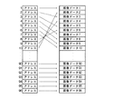
図3は、フラッシュメモリ27のデータ構造の一例を示している。図3に示す如く、フラッシュメモリ27は、画像データの並び順を管理するヘッダ部(アドレステーブル)と、画像データが実際に記憶される実画像データ部とからなっており、ヘッダ部は、何枚目(1〜96枚)かを示す順番データと実画像データ部の画像データの先頭アドレス(アドレスデータ)とが対応づけれらて格納されている。
また、図3に示す例では、1枚目の画像は画像データ1、2枚目は画像データ3、3枚目は画像データ4、4枚目は画像データ5、5枚目は画像データ7・・・、9枚目は画像データ6、10枚目は画像データ2、・・・96枚目は画像データ96が夫々対応している。
【0028】
ROM28は、デジタルカメラ1内で利用されるプログラムやデータ等を格納する。また、RAM29は、CPU31によって実行される各種処理におけるワークメモリを形成すると共に、後述する画像移動処理において、フラッシュメモリ27に格納されるヘッダ部のアドレスデータを一時的に格納するTEMPバッファ領域を有している。
【0029】
キー入力部30は、図1に示す「+」キー11、「−」キー12、「DEL」キー10、「DSP」キー14、「ZOOM」キー15等を含み、電子カメラ1における各種処理の選択に際して操作者が指示するためのものである。
【0030】
CPU31は、ROM28に記憶された各種プログラムに基づいて、RAM29の所定領域を作業領域に使用しつつ、キー入力部30の各キーの操作に応じた処理を実行して、デジタルカメラ1の各部を制御する。
【0031】
また、CPU31は、キー入力部30の「シャッター」キー9が操作されると、画像データ記憶処理を実行して、タイミングジェネレータ24に映像取り込み信号を発生して、CCD20から映像を取り込みDRAM25に一旦記憶させる。このDRAM25に記憶された画像データに対して、色演算処理をして、映像信号から輝度信号と色信号とを作成し、この輝度信号と色信号を圧縮/伸長回路26に転送して、輝度信号と色信号のデータを圧縮させ、この圧縮された画像データをフラッシュメモリ27に記憶する。
【0032】
また、CPU31は、キー入力部30の「DIP」キー14が操作されると、画像再生処理を実行して、フラッシュメモリ27から所定の圧縮した画像データ(圧縮輝度信号と色信号)を読み出して、圧縮/伸長回路26に転送し、この圧縮/伸長部回路26で伸長された輝度信号と色信号とをシグナルジェネレータ32に転送し、シグナルジェネレータ32にビデオ信号に変換させた後、LCD6に表示する。
【0033】
そして、CPU31は、詳細には後述する画像並び替え処理を実行して、フラッシュメモリ27のヘッダ部のアドレスデータの並び替えを行う(図4参照)。
【0034】
シグナルジェネレータ32は、デジタル画像データに同期信号を付加してデジタルビデオ信号を作成する。
【0035】
VRAM33は、シグナルジェネレータ32で生成されたビデオ信号を記憶するメモリである。
【0036】
D/A変換器34は、シグナル・ジェネレータ32から出力されたデジタルのビデオ信号をアナログのビデオ信号に変換する。
【0037】
LCD(Liquid Crystal Display)6は、入力されたビデオ信号に基づいて液晶を駆動して映像信号を表示する。
【0038】
I/Oポート36は、CPU31でシリアル信号に変換された画像データなどを入出力するインターフェースであり、FDD装置やパソコン等の外部装置が接続可能である。
【0039】
次に、本実施の形態のデジタルカメラの動作を説明する。
【0040】
図4は、デジタルカメラ1において、CPU31の制御により実行される画像並び替え処理を説明するためのフローチャートであり、図5〜図7は、LCD6の表示画面の表示例を示す図である。以下、図4のフローチャートに基づいて、図5〜図7を参照しつつかかる画像移動処理を説明する。
【0041】
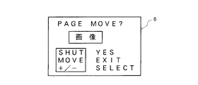
先ず、デジタルカメラの電源が投入されている状態で、キー入力部30の「DEL]キー10が押下されると、LCD6には、図5の如き、メニュー画面である”+:DELETE(削除)/−:MOVE(移動)”の画面が表示される(ステップS1)。
【0042】
次いで、CPU31は、移動(MOVE)を選択する「−」キー12が押下されたか否かを判断し(ステップS2)、「ー」キー12が押下されない場合は、画像データを削除する削除処理を実行する(ステップS11)。
【0043】
一方、ステップS2で、「ー」キー12が押下された場合は、図6の如き、移動元画像選択画面が表示され、「+」「−」キー11、12が操作されて移動元画像が選択されると(ステップS3)、図6の表示画面例に示す如く、上記選択された移動元画像の”画像”が表示される。
【0044】
次いで、CPU31は、移動元画像を確定する「シャッター」キー9が押下されたか否かを判断し(ステップS4)、「シャッター」キー9が押下されていない場合は、ステップS3に移行する一方、「シャッター」キー9が押下された場合は、選択された画像が移動元画像(移動対象画像)と確定され、CPU31は、フラッシュメモリ27のヘッダ部から移動元画像の先頭アドレスのデータを読み出して、RAM29のTEMPバッファ領域に一時的に格納する(ステップS5)。
【0045】
そして、図7の如き、9分割画面”画像1〜画像9”が表示され、「+」「ー」キー11、12の操作で画像下に白塗りが移動し、移動先画像選択される(ステップS7)。図7に示す表示例では、白塗りが画像1の下に移動して、画像1が選択されている。
【0046】
次いで、CPU31は、移動先画像を確定する「シャッター」キー9が押下されたか否かを判断し(ステップS8)、「シャッター」キー9が押下されていない場合は、ステップS6に移行する一方、「シャッター」キー9が押下された場合は、選択された画像が移動先画像と確定され、ステップS9に移行する。
【0047】
ステップS9では、移動元から移動先までのフラッシュメモリ27のヘッダ部の先頭アドレスデータをずらし、移動先のヘッダ部のアドレスにRAM29に一次的に格納されたアドレスデータを格納して(ステップS10)、当該画像並び替え処理を終了する。尚、上記各操作中に「DEL」キー10により移動を中止することができる。
【0048】
そして、上記画像移動処理による画像データの移動例を図8〜図11に基づいて説明する。尚、フラッシュメモリ27には、前記図3に示した構造のデータが格納されているものとする。
【0049】
図8及び図9は、3枚目の画像を10枚目の前に移動させる例を示す。
先ず、メニュー画面が選択されている状態で、「+」「ー」キー11、12の操作により移動元画像として画像3が選択されて(ステップS3)、「シャッター」キー9が押下されて移動元画像が確定すると(ステップS4)、図8に示す如く、3枚目のアドレスデータをRAM29のTEMPバッファ領域に一時的に格納し(ステップS5)、移動先である10枚目の画像を選択すると(ステップS7、S8)、4〜9枚までのアドレスデータを夫々3〜8に移動し(ステップS9)、次いで、RAM29のTEMPバッファ領域に格納した3枚目のアドレスデータを9枚目の位置に格納する(ステップS10)。かかる移動の結果、ヘッダ部とデータ部との対応は図9の如く、1枚目の画像は画像データ1、2枚目は画像データ3、3枚目は画像データ5、4枚目は画像データ7、5枚目は画像データ8、6枚目は画像データ9、7枚目は画像データ10、8枚目は画像データ6、9枚目は画像データ2、10枚目は画像データ2、11枚目は画像データ11、・・・・96枚目は画像データ96が夫々対応し、3枚目の画像が10枚目の画像の前に移動される。
【0050】
図10及び図11は、10枚目の画像を3枚目の前に移動させる例を示す。
先ず、メニュー画面が選択されている状態で、「+」「ー」キー11、12の操作により移動元画像として画像10が選択されて(ステップS3)、「シャッター」キー9が押下されて移動元画像が確定すると(ステップS4)、図10に示す如く、10枚目のアドレスをRAM29のTEMPバッファに一時的に格納し(ステップS5)、移動先である3枚目の画像を選択すると(ステップS7、S8)、3〜9枚までのアドレスデータを夫々4〜10に移動し(ステップS9)、次いで、RAM29に格納した10枚目のアドレスデータを3枚目の位置に格納する(ステップS10)。かかる移動の結果、ヘッダ部とデータ部との対応は図11の如く、1枚目の画像は画像データ1、2枚目は画像データ3、3枚目は画像データ2、4枚目は画像データ4、5枚目は画像データ5、6枚目は画像データ7、7枚目は画像データ8、8枚目は画像データ9、9枚目は画像データ10、10枚目は画像データ6、11枚目は画像データ11、・・・・96枚目は画像データ96が夫々対応し、10枚目の画像が3枚目の画像の前に移動される。
【0051】
以上説明したように、本実施の形態では、LCD6に分割表示された複数の画像データの中から、移動対象と移動先の画像が指定されると、フラッシュメモリ27のヘッダ部からは、移動対象として指定された画像データに対応するアドレスデータを読み出して、RAM29のTEMPバッファ領域に一時的に格納すると共に、移動元から移動先までの先頭アドレスデータをずらして、空いた移動先にRAM29のTEMPバッファ領域に一時的に格納されていたアドレスデータを格納して画像データの移動を行う構成である故、デジタルカメラ内で、画像データの並び換えが可能となる。
【0052】
尚、上記した実施の形態では、フラッシュメモリ27にヘッダ部(アドレステーブル)を格納する構成としたが、RAM29にヘッダ部を格納する構成としても良い。
【0053】
【発明の効果】
以上説明したように、請求項1記載の発明によれば、デジタルカメラの表示手段に表示されている画像を見ながら画像の順番を並び替えることができ、操作者の使い勝手が良くなる。
【0055】
また、選択手段で並び替え元を選択するとき表示手段に一度に1画像を表示させ、選択手段で並び替え先を選択するとき表示手段に一度に複数画像を表示させので、表示手段で表示されている並び替え先を素早く簡単に選択することができる。
【図面の簡単な説明】
【図1】本発明の実施の形態に係るデジタルカメラの外観構成を示す斜視図。
【図2】図1のデジタルカメラの回路構成を示すブロック図。
【図3】図2のフラッシュメモリに格納されるデータの構造の一例を示す図。
【図4】図2のCPUにより実行される画像並び替え処理を説明するためのフローチャート。
【図5】図4の画像並び替え処理でLCDに表示される画面の表示例1を示す図。
【図6】図4の画像並び替え処理でLCDに表示される画面の表示例2を示す図。
【図7】図4の画像並び替え処理でLCDに表示される画面の表示例3を示す図。
【図8】図4の画像並び替え処理による画像データの移動例を説明するための図。
【図9】図4の画像並び替え処理による画像データの移動例を説明するための図。
【図10】図4の画像並び替え処理による画像データの移動例を説明するための図。
【図11】図4の画像並び替え処理による画像データの移動例を説明するための図。
【符号の説明】
1 デジタルカメラ
4、5 ケース
6 LCD
7 撮像レンズ
8 「電源」キー
9 「シャッター」キー
10 「DEL」キー
11 「+」キー
12 「−」キー
13 「MODE」キー
14 「DIS」キー
15 「ZOOM」キー
16 「PROTECT]キー
17 開閉蓋
18 ファンクション切換キー
20 CCD
22 A/D変換器
23 駆動回路
24 タイミングジェネレータ
25 DRAM
26 圧縮/伸長回路
27 フラッシュメモリ
28 ROM
29 RAM
30 キー入力部
31 CPU
32 シグナルジェネレータ
33 VRAM
34 D/A変換器
35 アンプ
36 I/Oポート[0001]
BACKGROUND OF THE INVENTION
The present invention relates to a digital camera, and more particularly to a digital camera capable of rearranging images recorded on a recording medium in a digital camera provided with a display device.
[0002]
[Prior art]
Recently, digital cameras (electronic cameras) that electronically store captured images instead of film have become widespread. In such a digital camera, when a photographer presses a shutter, an image of a subject passing through a lens is captured by a CCD element, and is written on an internal recording medium through a circuit inside the camera. Then, the image written on the recording medium is reproduced.
[0003]
Recently, a digital camera which is integrally provided with a display device such as a liquid crystal and can immediately reproduce a photographed image at a photographing site has been put into practical use.
[0004]
[Problems to be solved by the invention]
Here, in order to organize images, there is a case where it is desired to change the order of recorded images or the order of reproduction.
However, in the conventional digital camera, the order of the image data recorded in the storage medium is changed by transferring all the photographed image data to an external editing device such as a personal computer, and the storage medium of the digital camera. After erasing all the image data stored in the computer, the images were transferred from the external editing device such as a personal computer to the digital camera one by one while viewing the images on the monitor. Otherwise, there was a problem that the order of the images could not be rearranged.
[0005]
Accordingly, the present invention has been made in view of the above problems, and an object of the present invention is to provide a digital camera that can rearrange images shot and recorded on a recording medium.
[0006]
[Means for Solving the Problems]
The invention according to
[0007]
In other words, according to the first aspect of the present invention, a digital camera having a display means, the subject is picked up by the image pickup means, the image data picked up by the image pickup means is stored in the storage means, and the reproduction means is this The image data stored in the storage means is reproduced and displayed on the display means, the selection means selects the image data reproduced by the reproduction means, and the rearranging means selects the image data selected by the selection means. Rearrange the order.
[0008]
Accordingly, the order of the images can be rearranged while viewing the images displayed on the display means of the digital camera, and the convenience for the operator is improved.
[0014]
Also, when selecting the sorting source by the selection means, one image is displayed at a time on the display means, and when selecting the sorting destination by the selection means, a plurality of images are displayed at a time on the display means. You can quickly and easily select the sorting destination.
[0015]
DETAILED DESCRIPTION OF THE INVENTION
Hereinafter, preferred embodiments to which the present invention is applied will be described with reference to FIGS.
FIGS. 1-11 is a figure which shows one Embodiment of the digital camera of this invention.
[0016]
First, the configuration will be described.
FIG. 1 is a perspective view showing an external configuration of a digital camera according to the present embodiment.
As shown in FIG. 1, the
An LCD (Liquid Crystal Display) 6 is provided in the
[0017]
In addition, an
[0018]
The
Further, a
[0019]
The camera unit 3 is arranged on the side surface on the left-hand operation side by the photographer with respect to the
[0020]
FIG. 2 is a block diagram showing a circuit configuration of the
FIG. 2 is a block diagram showing the configuration of the digital camera according to the embodiment of the present invention.
A
[0021]
The
[0022]
The A /
[0023]
The
[0024]
The
[0025]
The
[0026]
The compression /
[0027]
The
FIG. 3 shows an example of the data structure of the
In the example shown in FIG. 3, the first image is
[0028]
The
[0029]
The
[0030]
Based on various programs stored in the
[0031]
When the “shutter”
[0032]
Further, when the “DIP”
[0033]
The
[0034]
The
[0035]
The
[0036]
The D /
[0037]
An LCD (Liquid Crystal Display) 6 displays a video signal by driving a liquid crystal based on the input video signal.
[0038]
The I /
[0039]
Next, the operation of the digital camera of this embodiment will be described.
[0040]
FIG. 4 is a flowchart for explaining image rearrangement processing executed by the control of the
[0041]
First, when the “DEL” key 10 of the
[0042]
Next, the
[0043]
On the other hand, when the “−” key 12 is pressed in step S2, the movement source image selection screen is displayed as shown in FIG. 6, and the “+” and “−”
[0044]
Next, the
[0045]
Then, as shown in FIG. 7, a nine-divided screen “
[0046]
Next, the
[0047]
In step S9, the head address data of the header part of the
[0048]
An example of image data movement by the image movement process will be described with reference to FIGS. It is assumed that the
[0049]
8 and 9 show an example in which the third image is moved in front of the tenth image.
First, in a state where the menu screen is selected, the image 3 is selected as the movement source image by operating the “+” and “−”
[0050]
10 and 11 show an example in which the tenth image is moved in front of the third image.
First, in a state where the menu screen is selected, the image 10 is selected as the movement source image by operating the “+” and “−”
[0051]
As described above, in the present embodiment, when a movement target and a movement destination image are specified from among a plurality of image data divided and displayed on the
[0052]
In the above-described embodiment, the header portion (address table) is stored in the
[0053]
【The invention's effect】
As described above, according to the first aspect of the present invention, the order of the images can be rearranged while viewing the images displayed on the display means of the digital camera, and the usability for the operator is improved.
[0055]
Also, when selecting the sorting source by the selection means, one image is displayed at a time on the display means, and when selecting the sorting destination by the selection means, a plurality of images are displayed at a time on the display means. You can quickly and easily select the sorting destination.
[Brief description of the drawings]
FIG. 1 is a perspective view showing an external configuration of a digital camera according to an embodiment of the present invention.
FIG. 2 is a block diagram showing a circuit configuration of the digital camera of FIG.
FIG. 3 is a view showing an example of the structure of data stored in the flash memory of FIG. 2;
4 is a flowchart for explaining image rearrangement processing executed by the CPU of FIG. 2;
5 is a diagram showing a display example 1 of a screen displayed on the LCD in the image rearrangement process of FIG. 4;
6 is a diagram showing a display example 2 of a screen displayed on the LCD in the image rearrangement process of FIG. 4. FIG.
7 is a diagram showing a display example 3 of a screen displayed on the LCD in the image rearrangement process of FIG. 4;
FIG. 8 is a diagram for explaining an example of moving image data by the image rearrangement process of FIG. 4;
FIG. 9 is a diagram for explaining an example of moving image data by the image rearrangement process of FIG. 4;
10 is a diagram for explaining an example of movement of image data by the image rearrangement process of FIG. 4;
11 is a diagram for explaining an example of movement of image data by the image rearrangement process of FIG. 4;
[Explanation of symbols]
1
7
22 A /
26 Compression /
29 RAM
30
32
34 D /
Claims (1)
被写体を撮像する撮像手段と、
この撮像手段により撮像した画像を記憶する記憶手段と、
この記憶手段に記憶した画像を再生し、前記表示手段に表示させる再生手段と、
入力手段と、
所望の画像を選択する際に、前記記憶手段に記憶された画像のうちの1つの画像を前記再生手段によって前記表示手段に表示させるとともに、前記入力手段への入力にもとづいて所望の画像を選択させる選択手段と、
この選択手段により選択された画像の再生する順番を並び替える際に、前記記憶手段に記憶された画像データのうちの複数の画像を同時に前記再生手段によって前記表示手段に表示させるとともに、前記入力手段の入力によって前記再生手段に表示されている前記複数の画像のうちの 1 つを選択させることで、前記選択手段によって選択された所望の画像の再生する順番の並び替え位置を決定する並び替え手段と、
を備えたことを特徴とするデジタルカメラ。 In a digital camera equipped with a display means,
Imaging means for imaging a subject;
Storage means for storing an image captured by the imaging means;
Reproducing means for reproducing the image stored in the storage means and displaying the image on the display means;
Input means;
When selecting a desired image, one of the images stored in the storage means is displayed on the display means by the reproducing means, and a desired image is selected based on an input to the input means A selection means to
When rearranging the reproduction order of the images selected by the selection means, a plurality of images of the image data stored in the storage means are simultaneously displayed on the display means by the reproduction means, and the input means in the input thereby selecting one of the plurality of images displayed on said reproducing means, rearranging means for determining the sort position of the playback order of the desired image selected by said selection means When,
A digital camera characterized by comprising
Priority Applications (1)
| Application Number | Priority Date | Filing Date | Title |
|---|---|---|---|
| JP12055296A JP3620146B2 (en) | 1996-05-15 | 1996-05-15 | Digital camera |
Applications Claiming Priority (1)
| Application Number | Priority Date | Filing Date | Title |
|---|---|---|---|
| JP12055296A JP3620146B2 (en) | 1996-05-15 | 1996-05-15 | Digital camera |
Publications (2)
| Publication Number | Publication Date |
|---|---|
| JPH09307843A JPH09307843A (en) | 1997-11-28 |
| JP3620146B2 true JP3620146B2 (en) | 2005-02-16 |
Family
ID=14789141
Family Applications (1)
| Application Number | Title | Priority Date | Filing Date |
|---|---|---|---|
| JP12055296A Expired - Fee Related JP3620146B2 (en) | 1996-05-15 | 1996-05-15 | Digital camera |
Country Status (1)
| Country | Link |
|---|---|
| JP (1) | JP3620146B2 (en) |
Family Cites Families (11)
| Publication number | Priority date | Publication date | Assignee | Title |
|---|---|---|---|---|
| JPH02285872A (en) * | 1989-04-27 | 1990-11-26 | Sony Corp | Still picture filing device |
| JP3062695B2 (en) * | 1990-05-07 | 2000-07-12 | コニカ株式会社 | Still image video playback device |
| JPH0514847A (en) * | 1991-07-05 | 1993-01-22 | Kyocera Corp | Dubbing picture confirming system |
| JPH0530464A (en) * | 1991-07-19 | 1993-02-05 | Toshiba Corp | Moving image management device |
| JPH05197844A (en) * | 1992-01-21 | 1993-08-06 | Olympus Optical Co Ltd | Data processor |
| JP3250623B2 (en) * | 1992-03-04 | 2002-01-28 | オリンパス光学工業株式会社 | camera |
| JP3183712B2 (en) * | 1992-06-05 | 2001-07-09 | 京セラ株式会社 | Classification recording / reproduction method of electronic still camera |
| DE69322470T2 (en) * | 1992-08-12 | 1999-07-15 | Ibm | System and method for localizing video segment transitions |
| JP3584046B2 (en) * | 1992-09-09 | 2004-11-04 | キヤノン株式会社 | Image recording apparatus and method |
| JPH06303560A (en) * | 1993-04-13 | 1994-10-28 | Kyocera Corp | Multi-screen display system |
| JP3320197B2 (en) * | 1994-05-09 | 2002-09-03 | キヤノン株式会社 | Image editing apparatus and method |
-
1996
- 1996-05-15 JP JP12055296A patent/JP3620146B2/en not_active Expired - Fee Related
Also Published As
| Publication number | Publication date |
|---|---|
| JPH09307843A (en) | 1997-11-28 |
Similar Documents
| Publication | Publication Date | Title |
|---|---|---|
| JP3103151B2 (en) | Electronic still camera and operation control method thereof | |
| US6188432B1 (en) | Information processing method and apparatus for displaying and zooming an object image and a line drawing | |
| US20130271624A1 (en) | Information processing apparatus and method for operating same | |
| JP2004336495A (en) | Portable telephone unit | |
| JPH08205014A (en) | Electronic still camera | |
| US6952230B2 (en) | Information processing apparatus, camera and method for deleting data related to designated information | |
| JPH08223525A (en) | Display control method for image storage device and electronic still camera adopting same | |
| JP3777721B2 (en) | Image data storage device, image data storage method, imaging method, and storage medium | |
| US20010043278A1 (en) | Information input apparatus | |
| JP3620146B2 (en) | Digital camera | |
| JP3985102B2 (en) | Information input device | |
| JP3918228B2 (en) | Information processing apparatus and recording medium | |
| JP4235130B2 (en) | Digital camera | |
| JP4910862B2 (en) | Imaging apparatus and computer program therefor | |
| JP4099680B2 (en) | Information processing device | |
| JP3505914B2 (en) | Digital camera | |
| JP4227066B2 (en) | Image capturing apparatus and image reproducing method of image capturing apparatus | |
| JP4225434B2 (en) | Digital camera | |
| JP4437562B2 (en) | Information processing apparatus and storage medium | |
| JP3882270B2 (en) | Imaging device and storage medium | |
| JP2004193642A (en) | Digital camera | |
| JP2004040204A (en) | Image reproducing apparatus | |
| JP4210962B2 (en) | Electronic camera | |
| JP4536746B2 (en) | Electronic camera | |
| JPH09331495A (en) | Information input device |
Legal Events
| Date | Code | Title | Description |
|---|---|---|---|
| A977 | Report on retrieval |
Free format text: JAPANESE INTERMEDIATE CODE: A971007 Effective date: 20040427 |
|
| A131 | Notification of reasons for refusal |
Free format text: JAPANESE INTERMEDIATE CODE: A131 Effective date: 20040713 |
|
| A521 | Written amendment |
Free format text: JAPANESE INTERMEDIATE CODE: A523 Effective date: 20040909 |
|
| TRDD | Decision of grant or rejection written | ||
| A01 | Written decision to grant a patent or to grant a registration (utility model) |
Free format text: JAPANESE INTERMEDIATE CODE: A01 Effective date: 20041026 |
|
| A61 | First payment of annual fees (during grant procedure) |
Free format text: JAPANESE INTERMEDIATE CODE: A61 Effective date: 20041108 |
|
| R150 | Certificate of patent or registration of utility model |
Free format text: JAPANESE INTERMEDIATE CODE: R150 |
|
| FPAY | Renewal fee payment (event date is renewal date of database) |
Free format text: PAYMENT UNTIL: 20071126 Year of fee payment: 3 |
|
| FPAY | Renewal fee payment (event date is renewal date of database) |
Free format text: PAYMENT UNTIL: 20081126 Year of fee payment: 4 |
|
| FPAY | Renewal fee payment (event date is renewal date of database) |
Free format text: PAYMENT UNTIL: 20081126 Year of fee payment: 4 |
|
| FPAY | Renewal fee payment (event date is renewal date of database) |
Free format text: PAYMENT UNTIL: 20091126 Year of fee payment: 5 |
|
| FPAY | Renewal fee payment (event date is renewal date of database) |
Free format text: PAYMENT UNTIL: 20101126 Year of fee payment: 6 |
|
| FPAY | Renewal fee payment (event date is renewal date of database) |
Free format text: PAYMENT UNTIL: 20101126 Year of fee payment: 6 |
|
| FPAY | Renewal fee payment (event date is renewal date of database) |
Free format text: PAYMENT UNTIL: 20111126 Year of fee payment: 7 |
|
| FPAY | Renewal fee payment (event date is renewal date of database) |
Free format text: PAYMENT UNTIL: 20111126 Year of fee payment: 7 |
|
| FPAY | Renewal fee payment (event date is renewal date of database) |
Free format text: PAYMENT UNTIL: 20121126 Year of fee payment: 8 |
|
| FPAY | Renewal fee payment (event date is renewal date of database) |
Free format text: PAYMENT UNTIL: 20131126 Year of fee payment: 9 |
|
| LAPS | Cancellation because of no payment of annual fees |