JP3585701B2 - Cellular mobile communication system radio base station - Google Patents
Cellular mobile communication system radio base station Download PDFInfo
- Publication number
- JP3585701B2 JP3585701B2 JP15502297A JP15502297A JP3585701B2 JP 3585701 B2 JP3585701 B2 JP 3585701B2 JP 15502297 A JP15502297 A JP 15502297A JP 15502297 A JP15502297 A JP 15502297A JP 3585701 B2 JP3585701 B2 JP 3585701B2
- Authority
- JP
- Japan
- Prior art keywords
- signal
- phase
- receiver
- output
- antenna element
- Prior art date
- Legal status (The legal status is an assumption and is not a legal conclusion. Google has not performed a legal analysis and makes no representation as to the accuracy of the status listed.)
- Expired - Fee Related
Links
Images


Classifications
-
- H—ELECTRICITY
- H01—ELECTRIC ELEMENTS
- H01Q—ANTENNAS, i.e. RADIO AERIALS
- H01Q3/00—Arrangements for changing or varying the orientation or the shape of the directional pattern of the waves radiated from an antenna or antenna system
- H01Q3/26—Arrangements for changing or varying the orientation or the shape of the directional pattern of the waves radiated from an antenna or antenna system varying the relative phase or relative amplitude of energisation between two or more active radiating elements; varying the distribution of energy across a radiating aperture
- H01Q3/2605—Array of radiating elements provided with a feedback control over the element weights, e.g. adaptive arrays
-
- H—ELECTRICITY
- H01—ELECTRIC ELEMENTS
- H01Q—ANTENNAS, i.e. RADIO AERIALS
- H01Q3/00—Arrangements for changing or varying the orientation or the shape of the directional pattern of the waves radiated from an antenna or antenna system
- H01Q3/26—Arrangements for changing or varying the orientation or the shape of the directional pattern of the waves radiated from an antenna or antenna system varying the relative phase or relative amplitude of energisation between two or more active radiating elements; varying the distribution of energy across a radiating aperture
- H01Q3/267—Phased-array testing or checking devices
Landscapes
- Variable-Direction Aerials And Aerial Arrays (AREA)
- Mobile Radio Communication Systems (AREA)
Description
【0001】
【発明の属する技術分野】
本発明はセルラ移動通信システム無線基地局(以下、無線基地局と略す)に関し、特に、各セクタを指向するアンテナ素子で受信した受信信号を周波数変換した時の位相のずれを補正する位相補償に関するものである。
【0002】
【従来の技術】
自動車・携帯電話サービスをはじめとする各種移動通信サービスは、ここ数年、わが国だけでなく世界的にも目覚ましい発展を遂げている。移動通信の中でもセルラ方式による自動車・携帯電話サービスの発展は特に目覚ましい。
【0003】
セルラ方式による移動通信システムとは、各無線基地局のサービスゾーンである多数のセルでサービスエリアを覆う移動通信システムである。アンテナ素子の指向方向以外へのセルへ干渉を与えることが少なく、また、指向方向以外の移動局から到来する干渉波を除去するために、各セルを、複数、例えば、6個のセクタに分割して、各セクタを指向する複数のアンテナ素子でそのセクタ内に位置する移動局からの信号を受信している。
【0004】
各セクタを指向する複数のアンテナ素子で受信した受信信号は、LNA(Low Noise Amplifier)で低雑音増幅して、AGC回路を含むヘテロダイン構成された受信部により、ディジタルなベースバンドの直交するI,Q信号を生成(以下、受信信号をベースバンドに変換するまでの非線形素子で構成された回路を受信機と呼ぶ)して、ビームフォーマにより振幅ウェイト、位相回転を与えて合成することによって、所望のシャープなビームパターンに成形して、利得向上を図っている。
【0005】
このようにセルラ移動通信システムの無線基地局にディジタル信号処理によるマルチビームアンテナ、アダプティブアレーアンテナを適用すると、等価的にビームパターンをシャープにすることによる利得向上と、エリア内の干渉を低減する働きによって、1つのセルに収容できるユーザの数を比較的簡単に増大することができるものである。
【0006】
【発明が解決しようとする課題】
しかしながら、従来のディジタル信号処理によるビーム成形は、セルラ移動通信システムの無線基地局用としては未だ研究段階にあり、理想的な環境(各アンテナ素子の受信信号の受信機の出力(以下、アンテナブランチと呼ぶ)間の位相偏差が無い場合)を想定した計算機シミュレーションが殆どである。
【0007】
マルチビームアンテナ成形の場合では、アンテナブランチ間に位相偏差が無い場合を想定して複数のアンテナブランチの出力をビーム成形するために、LNA、ミキサなどの非線形素子、製作誤差、経年変化、温度特性などによるアンテナブランチ間に位相偏差がある場合には所望のビームパターンが得られず、特性の劣化を招くという問題があった。
【0008】
また、アダプティブアレーアンテナ成形の場合は、各アンテナブランチ間に位相偏差がある場合にも、それを含めて振幅、位相を制御するため問題としないことも考えられるが、位相偏差とアダプティブ処理の振幅、位相の制御量を分離しておくことは送信時に受信時の制御量から送信ビーム成形を行う場合には必要条件となるが、従来、この制御量を分離することができなかった。
【0009】
本発明は、このような点に鑑みてなされたものであり、セクタ内の特定ユーザ信号を用いて受信機の非線形素子などによる位相偏差をディジタル領域のビーム成形の前段階で補償し、効率の良いビーム成形を行うセルラ移動通信システム無線基地局を提供することを目的としている。
【0010】
【課題を解決するための手段】
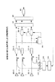
図1は、本発明の第1原理図である。
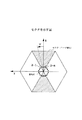
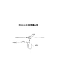
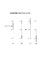
図2は、セクタを示す図である。
【0011】
図2において、無線基地局は、中心に位置しており、一定の範囲のセル内に位置する移動局を制御する。セルは、複数個(例えば、6個)のセクタに分割され、各セクタを指向するアンテナ素子2−k(k=1〜n)が配置されている。
【0012】
いずれのセクタについても同じことが言えるので、図2中の斜線で示すセクタについて説明する。このセクタに指向性を有する複数のアンテナ素子2−k(k=1〜n)が、Y軸に平行に配置されている。
【0013】
本発明は、各アンテナ素子2−k毎に設けられ、同じセクタを指向するアンテナ素子2−kで受信した信号から所望の周波数成分を抽出し、所定の帯域に周波数変換をする受信機4−kと、複数の受信機4−kの出力信号に基づいて、所望のビームパターンに成形するビームフォーマ6と、同じセクタを指向する複数のアンテナ素子2−kのうち、基準となるアンテナ素子を第1アンテナ素子2−1、該第1アンテナ素子2−1で受信した信号から周波数変換をする受信機を第1受信機4−1、第1アンテナ素子と異なる任意のアンテナ素子2−j(j=2〜n)を第2アンテナ素子2−j、該第2アンテナ素子2−jで受信した信号から周波数変換をする受信機4−jを第2受信機4−jとし、第1及び第2受信機4−1,4−jの出力信号を入力して、特定の上り信号の第1及び第2受信機4−1,4−jの出力信号を入力して、第1と第2受信機4−1,4−jとの出力信号の位相差と、第1と第2受信機4−1,4−jとの入力信号の位相差との差分の位相量を示す位相補償量を算出する位相補償量演算手段8−j(j=2〜n)と、第2受信機4−jの出力信号に対して、位相補償量から位相補正をする位相補償手段10−j(j=2〜n)とを具備したことを特徴とする。
【0014】
以上のように発明を構成したので、このセクタのエリア内にいるユーザ数をm、セクタに指向するアンテナ素子2−k(k=1〜n)のエレメント数をnとすると、受信機4−k(k=1〜n)のユーザ信号Xk(k=1〜n)は、次式(1)のように、複素数で表現される。
【0015】
X1=exp[(−1)1/2(αi (t)+φ1)]
X2=exp[(−1)1/2(αi (t)+Δθi2+ φ2)]
・
・
Xn=exp[(−1)1/2(αi (t)+Δθin+ φn )] ・・・(1)
但し、
αi (t) :i(i=1〜k)番目のユーザ信号の各受信経路における位相
Δθij:X1を基準としたとき、アンテナ素子2−kの配置とi番目のユーザからの到来波角度により決まるXjの位相回転
φj :受信機4−jの位相偏差を含む位相
(−1)1/2 :虚数単位
この信号を用いて、
Yj=Xj・X* 1=exp[(−1)1/2(φj −φ1+Δθij)] ・・・(2)
を計算する。
【0016】
但し、
*:複素共役
位相補償量演算手段8−jは、第1及び第2受信機4−1,4−jの出力信号X1,Xjを入力して、位相補償量ΔΦ=(φj −φ1 )を算出する。
【0017】
位相補償手段10−jは、第2受信機4−jの出力信号Xjに対して、次式(3)の位相補償を行う。
Aj=Xj・exp(−(−1)1/2ΔΦ)=exp[(−1)1/2(αi (t)+φ1 +Δθij)]…(3)
ところで、
X1=A1=exp[(−1)1/2(αi (t)+φ1 ) ] ・・・(4)
よって、位相補償手段10−jの出力信号Ajの位相項は、アンテナ配置と各ユーザからの到来波角度によって決まる位相回転項Δθijを除いて、基準としたアンテナ素子2−1の受信経路と同じとなり、位相補償が行われる。
【0018】
ビームフォーマ6は、この位相補償された信号を元に所望のビームパターンにビームフォーミングする。ビームフォーマ6に入力される信号は、位相補償手段10−jにより位相補償されているので、マルチビームアンテナ成形の場合では、ビームパターンの成形の効率が向上する。
【0019】
また、位相補償量演算手段8−kは、第1及び第2アンテナ素子2−1,2−jが指向するセクタ内に位置する移動局からの上り信号の中で、第1アンテナ素子2−1の出力信号と第2アンテナ素子2−jの出力信号との位相差を示す位相回転量の平均値が既知の値となる母集団に属する上り信号の第1及び第2受信機4−1,4−jの出力であることを示す制御信号を出力する制御手段と、制御信号に基づいて、第1受信機2−1の出力信号と第2受信機2−jとの位相差の平均値と、既知の値との差分を位相補償量として算出する平均化手段とを具備して構成してもよい。
【0020】
式(2)に示すように、第1受信機4−1の出力信号X1と第2受信機4−jの出力信号Xjとの位相差は、(φj −φ1+Δθij)となる。制御手段は、Δθijの平均値が既知の値ΔΘj となるような母集団に属する上り信号を用いるように、平均化手段を制御する。
【0021】
平均化手段は、次式(5)で示すX1とXjの位相差の平均値Bjを算出する。
【0022】
【数1】
![]()
式(5)に示すBjは、(φj −φ1+ΔΘj )に等しくなるものと推定される。そして、位相補償量は、BjからΔΘj を減算すると、その出力が、(φj −φ1)となる。位相補償手段10−jにより、Xjの位相(αi (t)+Δθij+ φj )から(φj −φ1)を引く位相補正をする。これにより、位相補償手段10−jの出力は、式(3)に示すようになって、位相補償される。
【0024】
図3は、本発明の第2原理図である。
本発明は、図3に示すように、第1位相補償量を入力して、第2受信機4−jの出力信号に対して、第1位相補償量に基づいて位相補正をする位相補償手段12−jと、第1受信機4−1の出力信号及び位相補償手段10−jの出力信号を入力して、第1受信機4−1の出力信号と位相補償手段10−jの出力信号との位相差と、第1と第2受信機4−1,4−jの入力信号の位相差との差分の位相量を示す第2位相補償量を算出する位相補償量演算手段8−jと、第2位相補償量と自身の出力信号とを加算して、第1位相補償量を位相補償手段10−jに出力する加算手段12−jとを具備して構成してもよい。
【0025】
上記第2位相補償量は、位相補償手段10−jの出力に対して、位相補償しなければならない位相補償量を示している。加算手段12−jにより、位相補償量演算手段8−jからの出力である第2位相補償量に現在の位相補償量である自身の出力を加算すると、第2受信機4−jに対する全体の第1位相補償量が得られる。
【0026】
そして、位相補償手段8−jは、この第1位相補償量に基づいて、第2受信機4−jの出力に対して、位相補償をする。これにより、位相補償手段10−jの出力は、式(3)に等しくなり、ビームフォーマ6には、位相の揃った信号が入力されることになり、マルチビームアンテナ成形の場合では、ビームパターンの成形の効率が向上する。
【0027】
また、位相補償量演算手段8−jは、第1及び第2アンテナ素子が指向するセクタ内に位置する移動局からの上り信号の中で、第1アンテナ素子2−1の出力信号に対する第2アンテナ素子2−jの出力信号の位相差を示す位相回転量の平均値が既知の値となる母集団に属する上り信号の第1受信機4−1及び位相補償手段10−jの出力であることを示す制御信号を出力する制御手段と、制御信号に基づいて、第1受信機4−1の出力信号に対する位相補償手段10−jの出力信号の位相差の平均値と既知の値との差分を位相補償量として算出する平均化手段とを具備して構成してもよい。
【0028】
また、制御手段は、第1及び第2アンテナ素子2−1,2−jが指向するセクタと該セクタの特定の隣接セクタとの境界近傍に位置する移動局に対してセクタ間ハンドオーバを行っている上り信号に基づく出力信号であることを示す制御信号を生成し、平均化手段は、既知の値として、セクタ間ハンドオーバを行う対象となる移動局の平均位置及び前記第1と第2アンテナ素子の位置に基づいて予め求められる値を使用してもよい。
【0029】
一般に、第1アンテナ素子2−1の出力に対する第2アンテナ素子2−jの出力の位相回転量は、上り信号を平面波と仮定すると、アンテナ素子2−1,2−jの配置方向に対する、上り信号の到来角により求められる。
【0030】
よって、移動局の母集団の平均の位置とアンテナ素子2−1,2−jの位置から、既知の値ΔΘj が予め求まる。この既知の値ΔΘj を用いて、位相補償量を算出して位相補償を行う。
【0031】
また、制御手段は、セルラ移動通信システム無線基地局から一定の距離に位置する特定の中心から一定の範囲内に位置する移動局に対して、セル間ハンドオーバを行っている上り信号に基づく出力信号であることを示す制御信号を生成し、平均化手段は、既知の値として、前記特定の中心の位置及び前記第1と第2アンテナ素子の位置に基づいて予め求められる値を使用するようにしてもよい。
【0032】
また、制御手段は、第1及び第2アンテナ素子2−1,2−jが指向する第1セクタの特定の隣接セクタを指向する任意の第3アンテナ素子の出力信号と該第1セクタを指向する任意の第4アンテナ素子の出力信号のレベルの差が閾値以下となる上り信号に基づく出力信号であることを示す制御信号を生成し、平均化手段は、既知の値として、レベルの差が閾値以下となる移動局の平均位置、前記第1と前記第2アンテナ素子の位置、及び該第3と第4アンテナ素子の放射パターンに基づいて予め求められる値を使用するようにしてもよい。
【0033】
第3及び第4アンテナ素子はそれぞれ特有の放射パターンを形成するので、隣接セクタを指向する任意のアンテナ素子の出力信号と第1セクタを指向する任意のアンテナ素子の出力信号のレベルの差が閾値以下となるものは、隣接セクタとの境界近傍からの上り信号であることが推定される。
【0034】
よって、この境界近傍の範囲を予め計算などにより求めて、その平均位置及び第1、第2アンテナ素子2−1,2−jの位置から位相回転量ΔΘj を推定することができる。この位相回転量ΔΘj を用いて、位相補償量を算出することができる。
【0035】
また、制御手段は、第1及び第2アンテナ素子2−1,2−jが指向する第1セクタに隣接する2つの隣接セクタをそれぞれ指向する任意の第3及び第4アンテナ素子の出力信号と前記第1セクタを指向する任意の第5アンテナ素子の出力信号とのレベルの差が共に閾値以上である上り信号に基づく出力信号であることを示す制御信号を生成し、平均化手段は、既知の値として、前記レベルの差が共に閾値以上となる移動局の平均位置、第1と第2アンテナ素子2−1,2−jの位置、及び該第3と第4、及び第5アンテナ素子の放射パターンに基づいて予め求められる値を使用するようにしてもよい。
【0036】
このレベルの差が共に閾値以上である上り信号は、セクタの中心方向の近傍付近に位置すると推定されるので、この近傍付近での平均の位置及び第1と第2アンテナ素子2−1,2−jの位置から位相回転量ΔΘj を推定することができる。この位相回転量ΔΘj を用いて、位相補償量を算出することができる。
【0037】
また、第1及び第2アンテナ素子が指向するセクタ内の既知の位置から信号を送出する信号発生装置を更に具備し、位相補償量演算手段8−jは、信号発生装置の既知の位置及び前記第1と第2のアンテナ素子の位置から求められる第1アンテナ素子2−1の出力信号に対する第2アンテナ素子2−jの出力信号の位相差に基づいて、信号発生装置からの上り信号を用いて位相補償量又は第2位相補償量を算出するようにしてもよい。
【0038】
また、第1及び第2アンテナ素子2−1,2−jが指向するセクタ内の既知の位置から信号を送出する信号発生装置を更に具備し、位相補償量演算手段は、信号発生装置の既知の位置及び前記第1と第2のアンテナ素子2−1,2−jの位置から求められる前記第1アンテナ素子2−1の出力信号と第2アンテナ素子2−jの出力信号との位相差に基づき、信号発生装置からの信号の前記第1及び第2受信機の出力信号を用いて位相補償量又は第1位相補償量を算出するようにしてもよい。
【0039】
また、セルラ移動通信システムが使用する無線帯域と同じ帯域の信号を生成して、信号線に出力する信号発生装置と、信号線からの信号に基づく第1信号を第1受信機4−1に出力する第1出力手段と、信号線からの信号に基づく第2信号を第2受信機4−jに出力する第2出力手段とを更に具備し、位相補償量演算手段は、第1信号と前記第2信号との既知の位相差に基づいて、第1信号の第1受信機4−1の出力信号及び第2信号の第2受信機4−jの出力信号を用いて前記位相補償量又は第1位相補償量を算出するようにしてもよい。
【0040】
さらに、第1アンテナ素子2−1の出力信号に基づく第1信号及び第2アンテナ素子2−jの出力信号のいずれかを第2受信機4−jに出力するスイッチ手段を更に具備し、位相補償演算手段は、第1アンテナ素子2−1の出力信号と第1信号との既知の位相差に基づき、第1受信機4−1の出力信号及び第1信号の第2受信機4−jの出力信号を用いて位相補償量又は第1位相補償量を算出するようにしてもよい。
【0041】
【発明の実施の形態】
以下、図面を参照して本発明の実施の形態について説明する。
第1実施形態
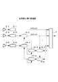
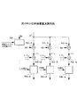
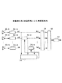
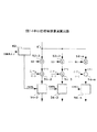
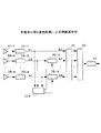
図4は、本発明の第1実施形態による無線基地局のブロック図ある。
【0042】
この図に示すように、無線基地局は、例えば、TDMA方式のセルラ移動通信システムであり、同じセクタを指向する複数のアンテナ素子30−k(k=1〜n)、アンテナ素子30−kのブランチ毎に受信機32−k(k=1〜n)、位相補償量演算回路34、位相補償回路36−j(j=2〜n)、ビームフォーマ38、ビームセレクタ40、及び復調回路42を具備する。
【0043】
図5は、図4中のアンテナ素子の配置図である。
図6は、リニアアレー座標系を示す図である。
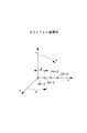
図5及び図6に示すように、セクタの中心方向をX軸、水平面におけるX軸に直交する軸をY軸とした時、アンテナ素子30−k(k=1〜n)は、そのセクタを指向するためにY軸方向に配置されている。図6中のZ軸は、右手系をなすように、X軸及びY軸に直交する方向にとっている。
【0044】
リニアアレーシステムでは、通常アンテナ素子30−k(k=1〜n)が等間隔d(例えば、上りの受信信号の波長λに等しい)で配置される。以下、リニアアレー座標系の原点に配置されたアンテナ素子30−1を基準として説明する。原点と移動局とを結ぶ直線とX軸とのなす角ψ、原点と移動局とを結ぶ直線とZ軸とのなす角ξとする。
【0045】
受信機32−k(k=1〜n)は、アンテナ素子30−kの出力信号から所定の周波数成分を抽出して、ディジタルな直交するベースバンド信号Ik,Qkを生成するものであり、図示はしないが、LNA、及びAGC回路を含むヘテロダインの受信部とにより構成される。
【0046】
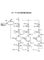
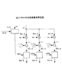
図7は、図4中の位相補償量演算回路の構成図である。
この図に示すように、位相補償量演算回路34は、制御回路50、乗算器52−j(j=2〜n)、加算器54−j(j=2〜n)、平均化部56−j(j=2〜n)を有する。
【0047】
制御回路50は、平均化部56−j(j=2〜n)において、加算器54−jの出力信号に対して平均値を取る対象を選択するための制御信号CNTLを生成する回路であり、平均値を取る対象に応じて回路構成される。
【0048】
例えば、特定の隣接セクタとセクタ間ハンドオーバを行っているユーザ信号を対象として選択する場合には、制御回路50は、例えば、1つの受信機32−kの出力信号Xkのパワーと隣接セクタの1つの受信機の出力信号のパワーがセクタ間ハンドオーバを行うレベルに達していることを示す制御信号CNTLを生成する回路構成となる。
【0049】
乗算器52−j(j=2〜n)は、受信機32−1の出力信号X1の複素共役X* 1(=(I1−(−1)1/2Q1))と受信機32−jの出力信号Xj(=(Ij+(−1)1/2Qj))との乗算をする回路である。
【0050】
加算器54−jは、乗算器52−jの出力Yjの位相argYjを求め、この位相argYjから平均化部56−jで平均値を求める対象となる移動局の平均位置から以下に説明するように予め算出しておいたアンテナ素子30−1の受信信号に対するアンテナ素子30−jの受信信号の位相回転量の平均値ΔΘj を減算するものである。尚、加算器54−jの位置は平均化部56−jの後であってもよい。
【0051】
図6に示すような座標系において、移動局がX軸から角度ψi 、Z軸から角度ξi に位置するi番目のユーザからの上り信号を各アンテナ素子30−j(j=2〜n)で受信した場合、上り信号を平面波、アンテナ素子30−1が原点、アンテナ素子30−jの原点からの距離がd(j−1)であると仮定すると、i番目のユーザ信号のアンテナ素子30−1の受信信号に対するアンテナ素子30−jの受信信号の位相回転量Δθijは、次式(6)に示すようになる。
【0052】
Δθij=(2π/λ)(j−1)dsinψi ・sinξi ・・・(6)
但し
λ:移動局の上り信号の波長
上記平均値ΔΘj (j=2〜n)は、対象となる複数のユーザについての位相回転量Δθijの平均値であり、平均値を求める対象の範囲を特定し、この対象の範囲にいるユーザの平均位置を式(6)に代入して予め計算により求めておいたものである。
【0053】
平均化部56−j(j=2〜n)は、図示はしないが、遅延回路、及び平均化回路を有する。遅延回路は、制御回路50の制御信号CNTLと加算器54−jの出力との同期を取るためのものであり、制御信号CNTLの加算器54−jの出力に対する遅れ時間だけ加算器54−jの出力を遅延させるものである。平均化回路は、制御信号CNTLが選択の指示(以下、アクティブと呼ぶ)を示す時に、遅延回路の出力に対して時間的な平均値を求めるものである。
【0054】
図8は、図4中の位相補償回路を示す図である。
位相補償回路36−jは、受信機32−jの出力Xjに対して、位相補償量演算回路34で算出された位相補正量Δφj だけ位相を補正するものであり、図8に示すように、位相補正量Δφj からexp[−(−1)1/2Δφj ] を求める演算回路60、及びXj・exp[−(−1)1/2Δφj ] を求める乗算器62を有する。
【0055】
ビームフォーマ38は、受信機32−1の出力X1(A1)、及び位相補償された位相補償回路36−j(j=2〜n)の出力Ajに対して、任意の振幅ウェイト、及び位相回転を与えて合成することにより、所望のビームパターンに成形するマルチビームアンテナ若しくはアダプティブアレーアンテナで構成されるディジタル信号処理回路である。
【0056】
ビームセレクタ40は、ビームフォーマ38の複数の出力のうち、所望ユーザ信号のレベルが最も強いビームを選択するものである。復調回路42は、π/4シフトQPSKなどの変調信号を復調する回路である。
【0057】
以下、これらの図を参照しつつ、第1実施形態による無線基地局の動作説明をする。
例えば、図2中の斜線で示されるセクタを指向するユーザの上り信号は、アンテナ素子30−k(k=1〜n)で受信されて、受信信号が受信機32−kに送られる。受信機32−kは、LNAで低雑音増幅、AGCで振幅等価、ヘテロダインの受信部によって、直交するディジタル信号Ik,Qkに変換する。
【0058】
ここで、ユーザ信号の受信機32−kの出力Xkは、次式(7)で表される。
Xk=exp[(−1)1/2(αi (t)+(k−1)Δθi + φk )] ・・・(7)
但し、
αi (t) :i番目ユーザ信号の各受信経路における位相
Δθi :X1を基準としたとき、アンテナ素子間隔dとi番目のユーザからの到来角度により決まる位相回転。
【0059】
φk :受信機32−kの位相偏差を含む位相
ここで、振幅偏差はAGCで補償されているため振幅は一定としている。
受信機32−1の出力X1は、ビームフォーマ38に入力され、出力X1の複素共役X* 1は、位相補償量演算回路34に入力される。受信機32−j(j=2〜n)の出力Xjは、位相補償量演算回路34及び位相補償回路36−jに入力される。
【0060】
一方、図7中の制御回路50は、1つの受信機32−k(i=1〜n)の出力Xkや隣接セクタを指向する1つのアンテナ素子の受信信号の受信機の出力などを入力して、以下に示す範囲にいる上りのユーザ信号を選択するための制御信号CNTLを生成して、平均化部56−j(j=2〜n)に出力する。
【0061】
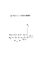
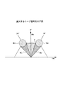
図9は、選択するユーザを示す図である。
この図に示すように、選択するユーザは、
・右に隣接するセクタとセクタ間ハンドオーバを行っているユーザHr
・左に隣接するセクタとセクタ間ハンドオーバを行っているユーザHl
・右上のエリアにいるセル間ハンドオーバを行っているユーザSr
・左上のエリアにいるセル間ハンドオーバを行っているユーザSl
・セクタの中で上記ユーザHr,Hl,Sr,Slを除くユーザC
である。
【0062】
(a) 右に隣接するセクタとセクタ間ハンドオーバを行っているユーザHr
制御回路50は、例えば、1つの受信機32−kの出力Xkのパワー(例えば、出力Xkを検波したその出力のパワー)と、右に隣接するセクタを指向する1つのアンテナ素子の受信信号の受信機の出力Xrのパワーがセクタ間ハンドオーバを行うレベルに達している時、制御信号CNTLをアクティブにし、これら以外の時に、制御信号CNTLをインアクティブにして、平均化部56−j(j=2〜n)に出力する。
【0063】
この場合、ユーザHrは、平均すると、右に隣接するセクタとの境界方向から信号が到来していることが分かる。すなわち、ユーザ信号は、ψ=30°、無線基地局からlの距離から到来する。
【0064】
従って、式(6)に示すΔθijを平均化すると、ψ=30°、無線基地局からlの距離に位置するユーザ信号の位相回転量に等しいものと推定される。よって、ΔΘj は、この位相回転量を予め計算しておくことにより得ることができる。
【0065】
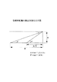
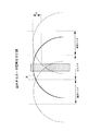
図10は、位相回転量の算出方法を示す図である。
無線基地局は、中心から半径Rのエリアをセルとして管理しているので、セクタ間ハンドオーバをしているユーザは、無線基地局からl=R/√2の距離に平均的に位置するものと推定される。
【0066】
図10に示すように、無線基地局のアンテナ素子30−k(k=1〜n)の高さをHとすると、無線基地局からR/√2の位置にいるユーザから見たアンテナ素子30−kの仰角αは次式(8)で表される。
【0067】
α=tan−1(√2H/R) ・・・(8)
よって、図6に示す座標系において、ユーザの位置座標(ψi ,ξi )=(π/6,α+π/2)となる。これを式(6)に代入することにより、ΔΘj が算出される。このΔΘj が図7中の加算器54−jの(−)端子に入力されている。
【0068】
一方、乗算器52−jは、受信機32−1の複素共役X* 1と受信機32−jの出力Xjとを乗算して、次式(9)で示す乗算器52−jの出力Yjを加算器54−jに出力する。
【0069】
Yj=Xj・X* 1=exp[j(φj −φ1+(j−1)Δθi )] ・・(9)
加算器54−jは、乗算器52−jの出力Yjの位相argYj(−π≦argYj≦π)を(+)端子に入力し、(j−1)Δθi の平均値ΔΘj を(−)端子に入力して、argYj−ΔΘj を計算して、平均化部56−jに出力する。
【0070】
平均化部56−jは、加算器54−jの出力を入力して、遅延回路により、遅延させて、制御信号CNTLと同期を取る。平均化回路により、制御信号CNTLがアクティブであれば、スタックしておいた加算器54−jの出力に対して時間的な平均値を求めて、図4中の位相補償回路36−jに位相補償量Δφj を出力する。
【0071】
式(9)の位相(φj −φ1+(j−1)Δθi )の平均値は、(φj −φ1 +ΔΘj )であると推定されるので、平均化部56−jの出力Δφj は、(φj −φ1 )に等しくなる。
【0072】
ここで、−π≦argYj−ΔΘj ≦πとしているので、図11(a)に示すように、{argYj−ΔΘj }の集合が連続すれば問題はないが、同図(b)に示すように、πを上限とする第1部分と−πを下限とする第2部分とに離間した集合となる場合は、そのまま平均値を求めると正しい結果が得られないので、平均化部56−jは、同図(c)に示すように、第2部分を2πだけシフトする、もしくは、同図(d)に示すように、第1部分を−2πだけシフトして連続するように調整してから平均値を求める。
【0073】
位相補償回路36−jは、図8中の演算器60により、exp[−jΔφj ] を求めて、乗算器62に出力する。乗算器62は、受信機32−jの出力Xjにexp[−jΔφj ] を掛け合わせて、次式(10)に示すAjをビームフォーマ38に出力する。
【0074】
Aj=Xj・exp[−(−1)1/2Δφj ]=exp[(−1)1/2(αi (t)+φ1+(j−1) Δθi )]・・・(10)
ところで、
X1=A1=exp[(−1)1/2(αi (t)+φ1 )] ・・・(11)
よって、j番目の受信経路の位相項は、アンテナ配置と各ユーザからの到来波角度により決まる位相回転の項を除いて、基準として1番目の受信経路と同じとなり、位相補償が行われる。
【0075】
ビームフォーマ38は、受信機31−1の出力A1(=X1)及び位相補償された出力Aj(j=2〜n)を入力して、マルチビームアンテナ、又はアダプティブアレーアンテナシステム構成により、ディジタル信号処理を行う。マルチビームアンテナにおいては、入力の位相が補償されているので、ビーム成形の効率が良くなる。
【0076】
ビームセレクタ40は、ビームフォーマ38の複数の出力のうち、所望ユーザ信号のレベルが最も強いビームを選択して、復調回路42に出力する。復調回路42は、π/4シフトQPSKなどの変調信号を復調する。
【0077】
(b) 左に隣接するセクタとセクタ間ハンドオーバを行っているユーザHl
ユーザHlは、平均すると、左に隣接するセクタとの境界方向から信号が到来していることが分かる。すなわち、ユーザ信号は、ψ=30°、無線基地局からR/√2の距離から到来する。よって、図6に示す座標系において、ユーザの位置座標(ψi ,ξi )=(−π/6,α+π/2)となる。これを式(6)に代入することにより、平均値ΔΘj が得られる。
【0078】
このΔΘj を用いて、(a)の場合と同様にして、位相補償量演算回路34にて、位相補償量Δφj を求めて、位相補償回路36−jにて、Xjに対して、Xj・exp [−(−1)1/2 Δφj ] を求めて、ビームフォーマ38に出力する。
【0079】
(c) 右上のエリアにいるセル間ハンドオーバを行っているユーザSr
ユーザSrは、平均すると、その中心に位置する方向から信号が到来していることが分かる。すなわち、ユーザ信号は、ψ=30°、無線基地局からRの距離から到来する。よって、図10に示すように、ユーザの位置座標(ψi ,ξi )=(π/6,β+π/2)(β=tan −1( H/R))となる。これを式(6)に代入することにより、平均値ΔΘj が得られる。
【0080】
このΔΘj を用いて、(a)の場合と同様にして、位相補償量演算回路34にて、位相補償量Δφj を求め、位相補償回路36−jにて、Xjに対して、Xj・exp [−j Δφj ] を求めて、ビームフォーマ38に出力する。
【0081】
(d) 左上のエリアにいるセル間ハンドオーバを行っているユーザSl
ユーザSlは、平均すると、その中心に位置する方向から信号が到来していると推定される。すなわち、ユーザ信号は、ψ=−30°、無線基地局からRの距離から到来しているものと推定される。よって、図10に示すように、ユーザの位置座標(ψi ,ξi )=(−π/6,β+π/2)(β=tan −1( H/R))となる。これを式(6)に代入することにより、平均値ΔΘj が得られる。
【0082】
このΔΘj を用いて、(a)の場合と同様にして、位相補償量演算回路34にて、位相補償量Δφj を求め、位相補償回路36−jにて、Xjに対して、Xj・exp [−j Δφj ] を求めて、ビームフォーマ38に出力する。
【0083】
(e) ユーザC
ユーザCは、平均すると、セクタの中心方向から信号が到来していると推定される。すなわち、ユーザ信号は、ψ=0°、無線基地局からR/√2の距離から到来していると推定される。よって、ユーザの位置座標(ψi ,ξi )=(0,α+π/2)となる。これを式(6)に代入することにより、平均値ΔΘj =0が得られる。
【0084】
このΔΘj =0を用いて、(a)の場合と同様にして、位相補償量演算回路34にて、位相補償量Δφj を求め、位相補償回路36−jにて、Xjに対して、Xj・exp [−j Δφj ] を求めて、ビームフォーマ38に出力する。
【0085】
以上説明した第1実施形態によれば、位相補償量演算回路34により位相補償量を算出して、位相補償回路36−jにて、受信機32−jの出力Xjに対して、位相補償をするので、ビームフォーマ38に位相の揃った信号が入力されて、マルチビームアンテナシステムのビームフォーマでは、ビーム成形の効率が良くなる。また、アダプティブアンテナシステムのビームフォーマの場合は、位相偏差、アダプティブ処理の振幅、位相の制御量を分離することができて、送信時に受信時の位相偏差量から送信ビーム成形を行うことができる。
【0086】
第2実施形態
図12は、本発明の第2実施形態による無線基地局のブロック図あり、図4中の要素と同一の機能を有する要素には同一の符号を付してある。
【0087】
この図に示すように、無線基地局は、例えば、TDMA方式のセルラ移動通信システムであり、同じセクタを指向する複数のアンテナ素子30−k(k=1〜n)、受信機32−k(k=1〜n)、位相補償量演算回路70、位相補償回路36−j(j=2〜n)、ビームフォーマ38、ビームセレクタ40、及び復調回路42を具備する。
【0088】
アンテナ素子30−k、受信機32−k(k=1〜n)、位相補償回路36−j(j=2〜n)、ビームフォーマ38、ビームセレクタ40、及び復調回路42は、図4中のものと同じであり説明を省略する。
【0089】
図13は、図12中の位相補償量演算回路の構成図であり、図7中の要素と同一の機能を有する要素には同一の符号を付してある。
この図に示すように、位相補償量演算回路70は、制御回路50、乗算器52−j(j=2〜n)、加算器54−j(j=2〜n)、平均化部56−j(j=2〜n)、及び加算器72−j(j=2〜n)を有する。
【0090】
制御回路50は、図7中のものと同一である説明を省略する。乗算器52−j(j=2〜n)は、受信機32−1の出力X1の複素共役X* 1と位相補償回路54−jの出力Ajとの乗算を行うものである。加算器54−j、及び平均化部56−j(j=2〜n)は、図7中のものと同じであり説明を省略する。加算器72−jは、平均化部56−jの出力と自身の出力とを加算するものである。
【0091】
以下、これらの図を参照しつつ、第2実施形態による無線基地局の動作説明をする。
例えば、図2中の斜線で示されるセクタを指向するユーザの上り信号は、アンテナ素子30−k(k=1〜n)で受信されて、受信信号が受信機32−kに送られる。受信機32−kは、LNAで低雑音増幅、AGCで振幅等価、ヘテロダインの受信部によって、直交するディジタル信号Ik,Qkに変換する。
【0092】
受信機32−1の出力X1は、ビームフォーマ38に入力され、X1の複素共役X* 1は、位相補償量演算回路70に入力される。受信機32−j(j=2〜n)の出力Xjは、位相補償回路36−jに入力される。
【0093】
位相補償回路36−jは、受信機32−jの出力Xjと位相補償量演算回路70より出力される位相量Δρj のexp[−jΔρj ] との乗算して、次式(12)で示される出力Ajを、位相補償量演算回路70及びビームフォーマ38に出力する。
【0094】
Aj=exp[(−1)1/2(αi (t)+(j−1) Δθi + φj −Δρj )] ・・・(12)
位相補償量演算回路70中の乗算器52−jは、X* 1と位相補償回路36−jの出力Ajとを乗算して、次式(13)に示す出力Yjを加算器54−jに出力する。
【0095】
Yj=exp[(−1)1/2(φj − φ1 −Δρj + ( j−1) Δθi )]・・・(13)
加算器54−jは、(+)端子に入力される乗算器52−jの出力Yjの位相argYj(−π≦argYj≦π)から(j−1)Δθi の平均値Θj を減算して、平均化部56−jに出力する。尚、加算器54−jの位置は平均化部56−jの後であってもよい。
【0096】
平均化部56−jは、制御回路50からの制御信号CNTLに従って、加算器54−jの出力の時間的な次式(14)に示す平均値Zjを求め、加算器72−jに出力する。
【0097】
Zj=φj − φ1 −Δρj ・・・(14)
加算器72−jは、平均化部56−jの出力に自身の現時点での位相補正量Δρj を加算して、その加算結果(φj − φ1 )を位相補償回路36−jに出力する。これにより、位相補償回路36−jは、この位相補償量(φj − φ1 )から受信機32−jの出力Xjに対して位相補正して、ビームフォーマ38及び位相補正量演算回路70に出力する。
【0098】
この時点において、位相補償回路36−jにより、受信機32−jの出力Xjは、正しく位相補償されているので、平均化部56−jの出力は、0となり、加算器72−jの出力は、変化しない。
【0099】
ビームフォーマ38は、受信機32−1の出力X1及び位相補償された出力Aj(j=2〜n)を入力して、マルチビームアンテナ、又はアダプティブアレーアンテナシステム構成により、ディジタル信号処理を行う。マルチビームアンテナにおいては、入力の位相が補償されているので、ビーム成形の効率が良くなる。
【0100】
ビームセレクタ40は、ビームフォーマ38の複数の出力のうち、所望ユーザ信号のレベルが最も強いビームを選択して、復調回路42に出力する。復調回路42は、π/4シフトQPSKなどの変調信号を復調する。
【0101】
以上説明した第2実施形態によれば、第1実施形態と同様に、マルチビームアンテナシステムのビームフォーマでは、ビーム成形の効率が良くなる。また、アダプティブアンテナシステムのビームフォーマの場合は、位相偏差、アダプティブ処理の振幅、位相の制御量を分離することができて、送信時に受信時の位相偏差量から送信ビーム成形を行うことができる。
【0102】
第3実施形態
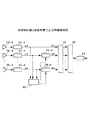
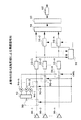
図14は、本発明の第3実施形態による無線基地局の機能ブロック図あり、図4中の要素と同一の機能を有する要素には同一の符号を付してある。
【0103】
この図に示すように、無線基地局は、例えば、TDMA方式のセルラ移動通信システムであり、同じセクタを指向する複数のアンテナ素子30−k(k=1〜n)、受信機32−k(k=1〜n)、位相補償量演算回路80、位相補償回路36−j(j=2〜n)、ビームフォーマ38、ビームセレクタ40、及び復調回路42を具備する。
【0104】
アンテナ素子30−k、受信機32−k(k=1〜n)、位相補償回路36−j(j=2〜n)、ビームフォーマ38、ビームセレクタ40、及び復調回路42は、図4中のものと同じであり説明を省略する。
【0105】
図15は、図14中の位相補償量演算回路80の構成図であり、図7中の要素と同一の機能を持つ要素には共通の符号を付してある。
制御回路82は、既知の位置にいる特定の上りの信号を対象とするように、制御信号CNTLを生成するものであり、例えば、図示しないが、ユーザが未使用の時間帯に、基地局を管理する図示しない交換機などから通信回線を通して、ユーザ信号の選択を指示する信号を受信して、制御信号CNTLを平均化部56−j(j=2〜n)に出力する構成にしている。
【0106】
加算器54−jに入力されるΔΘj は、ユーザ信号の既知の位置uとアンテナ素子30−kの配置とにより、後述するように、式(6)から予め算出された値である。乗算器52−j、加算器54−j、及び平均化部56−jは、図7中のものと同じであり説明を省略する。
【0107】
図16は、上り信号発生装置の位置を示す図である。
以下、これらの図を参照ししつ、第3実施形態による無線基地局の動作説明をする。
【0108】
位相補償量を算出するために、交換機などから、位相補償量の算出を指示する信号が通信回線を介して無線基地局の制御回路82で受信される。制御回路82は、この信号を受信して、位相補償量の算出を指示する制御信号CNTLを平均化部56−j(j=2〜n)に出力する。
【0109】
一方、この制御信号CNTLと同期して、図16に示す位置uに配置された上り信号発生装置84から発生した上り信号がアンテナ素子30−k(k=1〜n)で受信されて、受信信号が受信機32−kに送られる。受信機32−kは、LNAで低雑音増幅、AGCで振幅等価、ヘテロダインの受信部によって、直交するディジタル信号Ik,Qkに変換する。
【0110】
受信機32−1の出力X1は、ビームフォーマ38に入力され、X1の複素共役X* 1は、位相補償量演算回路80に入力される。受信機32−j(j=2〜n)の出力Xjは、位相補償回路36−jに入力される。
【0111】
乗算器52−jは、X1* ・Xjを求めて、加算器54−jに出力する。図16に示すように、上り信号発生装置84の位置uはX軸とのなす角ψ及び位置uと無線基地局との距離はr、アンテナ素子30−kの高さはHである。位置uでは、図16(b)に示すように、ξ=(π/2+γ)(γ=tan −1(H/γ))となり、このξを式(6)に代入することにより算出されたΔΘj が加算器54−jの(−)端子に入力されている。
【0112】
加算器54−jは、(+)端子に入力される乗算器52−jの出力Yjの位相argYj(−π≦argYj≦π)から(−)端子に入力されるΔΘj を減算して、平均化部56−jに出力する。尚、加算器54−jの位置は平均化部56−jの後であってもよい。
【0113】
平均化部56−jは、制御回路80からの制御信号CNTLに従って、加算器54−jの出力の平均値を算出して、位相補償量Δφj を位相補償回路36−jに出力する。ここで、平均化部56−jにより平均値を求めているのは、上り信号発生装置84の位置が既知なので第1実施形態などのように統計的な平均を取って位相回転量を推定する必要はないが、この平均を取ることにより、位相補償量Δφj の精度が向上するからである。
【0114】
そして、位相補償量Δφj が算出されると、交換機などから、位相補償量の算出を停止する指示する信号を制御回路82が受信して、制御信号CNTLをインアクティブにする。
【0115】
一方、上りのユーザ信号は、アンテナ素子30−k(k=1〜n)で受信され、受信機32−kで直交するベースバンド信号に変換される。位相補償回路36−jは、受信機32−j(j=2〜n)の出力Xjに対して、位相補償量演算回路80より既に算出されて位相補償量Δφj に従って位相補償をして、ビームフォーマ38に出力する。
【0116】
ビームフォーマ38は、受信機32−1の出力A1(=X1)及び位相補償された出力Aj(j=2〜n)を入力して、マルチビームアンテナ、又はアダプティブアレーアンテナシステム構成により、ディジタル信号処理を行う。マルチビームアンテナにおいては、入力の位相が補償されているので、ビーム成形の効率が良くなる。
【0117】
ビームセレクタ40は、ビームフォーマ38の複数の出力のうち、所望ユーザ信号のレベルが最も強いビームを選択して、復調回路42に出力する。復調回路42は、π/4シフトQPSKなどの変調信号を復調する。
【0118】
以上説明した第3実施形態によれば、第1実施形態と同様の効果がある。
第4実施形態
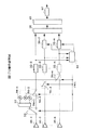
図17は、本発明の第4実施形態による無線基地局のブロック図であり、図4中の要素と同一の機能を有する要素には同一の符号を付してある。
【0119】
この図に示すように、無線基地局は、例えば、TDMA方式のセルラ移動通信システムであり、同じセクタを指向する複数のアンテナ素子30−k(k=1〜n)、受信機32−k(k=1〜n)、スイッチ回路90、分配器92、移相器94−k(k=1〜n)、スイッチ回路96−k(k=1〜n)、位相補償量演算回路98、位相補償回路36−j(j=2〜n)、ビームフォーマ38、ビームセレクタ40、及び復調回路42を具備する。
【0120】
アンテナ素子30−k、受信機32−k(k=1〜n)、位相補償回路36−j(j=2〜n)、ビームフォーマ38、ビームセレクタ40、及び復調回路42は、図4中のものと同じであり説明を省略する。
【0121】
スイッチ回路90は、アンテナ素子30−1と分配器92とのオン/オフをするものであり、位相補償量演算回路98により出力される制御信号CNTLにより制御されるものである。
【0122】
分配器92は、アンテナ素子30−1の出力を移相器94−k(k=1〜n)に分配するものである。移相器94−k(k=1〜n)は、受信機32−kへの入力信号の位相を移相器94−kから受信機32−kまでの伝送線路長の違いなどによる位相のずれを補償して、受信機32−jへの入力信号の位相と受信機32−1の入力信号との位相差が所望、例えば、位相差が0になるように位相を調整するためのものである。
【0123】
スイッチ回路96−k(k=1〜n)は、アンテナ素子30−kの出力又は移相器94−kの出力のいずれかを受信機32−kに出力するためのものであり、位相補償量演算回路98により出力される制御信号CNTLにより制御されるものである。
【0124】
位相補償量演算回路98は、受信機32−j(j=2〜n)の出力Xjに対する位相補償量を算出する回路であり、本例では、受信機32−jの出力Xjと受信機32−1の出力X1の位相差〔(φj −φ1 )+ΔΘj 〕中のΔΘj は、移相器94−1,94−jにより位相調整されており、例えば、ΔΘj =0である。
【0125】
位相補償量演算回路98中の制御回路は、受信機32−k(k=1〜n)への入力信号を選択するために、例えば、図示しない交換機などから、ユーザが未使用の時間帯に、位相補償量の算出を指示する信号を受信して、平均化部やスイッチ回路90,96−k(k=1〜n)に制御信号CNTLを出力するものである。
【0126】
図18は、図17の動作説明図である。
以下、これらの図を参照しつつ、第4実施形態によるセルラ移動通信システム無線基地局の動作説明をする。
【0127】
例えば、ユーザが使用していない時間帯などにおいて、位相補償量演算回路98中の図示しない制御回路は、図示しないが複数の無線基地局を管理する交換局などから、位相補償量の算出を指示する信号を受信して、制御信号CNTLをスイッチ回路90,96−k(k=1〜n)、及び平均化部に出力する。
【0128】
スイッチ回路90は、図18に示すように、制御信号CNTLに従い、アンテナ素子30−1の出力端子と分配器92の入力端子とを接続する。また、スイッチ回路96−k(k=1〜n)は、制御信号CNTLに従って、移相器94−kの出力端子と受信機32−kの入力端子とを接続する。
【0129】
一方、この制御信号CNTLに同期して、セクタに位置する移動局などの送信機より、上りの信号を無線基地局に送信する。アンテナ素子30−k(k=1〜n)は、この上りの信号を受信して、スイッチ回路90,96−k(k=1〜n)に出力する。
【0130】
アンテナ素子30−1の出力は、スイッチ回路90を介して、分配器92に入力される。分配器92は、アンテナ素子30−1の出力を入力して、各移相器94−k(k=1〜n)に分配する。移相器94−kは、受信機32−kに入力する位相をそれぞれ所望の位相に揃わせる、例えば、受信機32−1と同相にするために、一定の位相補正量で分配器92の出力を位相補正して、スイッチ回路96−kに出力する。
【0131】
スイッチ回路96−kは、受信機32−kに出力する。このため、受信機32−j(j=2〜n)への入力信号は、受信機32−1の入力信号と同相もしくは既知の値ΔΘj だけずれている。
【0132】
受信機32−1は、スイッチ回路96−1の出力を入力して、直交するベースバンドの信号に変換して、ビームフォーマ38に出力し、その複素共役を位相補償量演算回路98に出力する。受信機32−j(j=2〜n)は、位相補償回路36−j及び位相補償量演算回路98に出力する。
【0133】
位相補償量演算回路98は、図示しない乗算器にて、受信機32−1の出力X1の複素共役X* 1と受信機32−jの出力Xjとの乗算をして、加算器にて、乗算器の出力の位相から移相器94−j(j=2〜n)によって調整された既知の位相差ΔΘj 、例えば、移相器94−1の出力と同相であれば0を減算して、平均化部に出力する。そして、平均化部にて、制御信号CNTLに従って、平均値を求めて、位相補償回路36−jに位相補償量Δφj を出力する。
【0134】
位相補償量Δφj が算出されると、例えば、交換機は、位相補償量の算出の停止を指示する信号を位相補償量演算回路98に送信する。位相補償量演算回路98は、この信号を受信して、図17に示すように、アンテナ素子30−k(k=1〜n)の出力端子と受信機32−kの入力端子とを接続するように、スイッチ回路90、96−k(k=1〜n)を制御する。
【0135】
そして、ユーザからの上り信号は、アンテナ素子30−k(k=1〜n)で受信されて、受信機32−k(k=1〜n)で直交するベースバンド信号に変換される。受信機32−j(j=2〜n)の出力は、位相補償回路36−jにて、既に位相補償量演算回路98にて算出された位相補償量Δφj に従って、位相補償されて、ビームフォーマ38に出力される
ビームフォーマ38は、受信機32−1の出力A1(=X1)及び位相補償された出力Aj(j=2〜n)を入力して、マルチビームアンテナ、又はアダプティブアレーアンテナシステム構成により、ディジタル信号処理を行う。マルチビームアンテナにおいては、入力の位相が補償されているので、ビーム成形の効率が良くなる。
【0136】
ビームセレクタ40は、ビームフォーマ38の複数の出力のうち、所望ユーザ信号のレベルが最も強いビームを選択して、復調回路42に出力する。復調回路42は、π/4シフトQPSKなどの変調信号を復調する。
【0137】
以上説明した第4実施形態によれば、第1実施形態と同様の効果がある。
第5実施形態
図19は、本発明の第5実施形態による無線基地局のブロック図であり、図4中の要素と同一の機能を有する要素には同一の符号を付してある。
【0138】
この図に示すように、無線基地局は、例えば、TDMA方式のセルラ移動通信システムであり、同じセクタを指向する複数のアンテナ素子30−k(k=1〜n)、信号発生装置100、分配器102、移相器104−k(k=1〜n)、カプラ106−k(k=1〜n))、受信機32−k(k=1〜n)、位相補償量演算回路108、位相補償回路36−j(j=2〜n)、ビームフォーマ38、ビームセレクタ40、及び復調回路42を具備する。
【0139】
アンテナ素子30−k(k=1〜n)、受信機32−k(k=1〜n)、位相補償回路36−j(j=2〜n)、ビームフォーマ38、ビームセレクタ40、及び復調回路42は、図4中のものと同じであり説明を省略する。
【0140】
信号発生装置100は、高周波信号を生成する装置であり、例えば、無線基地局の無線帯域の高周波信号を生成するものである。分配器102は、信号発生装置100で生成した高周波信号を移相器104−k(k=1〜n)に分配するものである。
【0141】
移相器104−k(k=1〜n)は、受信機32−k(k=1〜n)への入力信号の位相を移相器104−kから受信機32−kまでの伝送線路長の違いやカプラ106−kの特性の違いなどによる位相のずれを補償して、受信機32−j(j=2〜n)への入力信号の位相と受信機32−1の入力信号との位相差が所望、例えば、位相差が0になるように、その位相を補正するためのものである。
【0142】
カプラ106−k(k=1〜n)は、アンテナ素子30−kの出力と移相器104−kの出力とを合波するものである。位相補償量演算回路108は、位相補償量を算出する回路である。
【0143】
以下、図19に示す第5実施形態による無線基地局の動作説明をする。
例えば、ユーザが使用していない時間帯などにおいて、位相補償量演算回路108中の図示しない制御回路は、図示しないが複数の無線基地局を管理する交換局などから、位相補償量の算出を指示する信号を受信して、制御信号を平均化部に出力する。
【0144】
信号発生装置100は、制御信号に同期して、例えば、制御信号を入力して、所定の周波数の信号を生成して、分配器102に出力する。分配器102は、信号発生装置100の出力を入力して、移相器104−k(k=1〜n)に分配する。
【0145】
移相器104−kは、受信機32−kに入力する位相がそれぞれ所望の位相に揃わせるために、例えば、受信機32−1と同相にするために一定の位相補正量で分配器102の出力を位相補正して、カプラ106−kに出力する。
【0146】
カプラ106−kは、アンテナ素子30−kの出力と移相器104−kの出力とを合波して、受信機32−kに出力する。この受信機32−j(j=2〜n)への入力は、受信機32−1の入力と所望の位相差ΔΘj 、例えば、ΔΘj =0となる。
【0147】
受信機32−1は、カプラ106−1の出力を入力して、直交するベースバンドの信号に変換して、ビームフォーマ38に出力し、その複素共役を位相補償量演算回路108に出力する。受信機32−j(j=2〜n)は、カプラ106−jの出力を入力して、位相補償回路36−j及び位相補償量演算回路108に直交するベースバンドの信号を出力する。
【0148】
位相補償量演算回路108は、図示しない乗算器にて、受信機32−1の出力X1の複素共役X* 1と受信機32−jの出力Xj(j=2〜n)との乗算をして、加算器にて、乗算器の出力の位相から移相器104−j(j=2〜n)によって調整された既知の位相差ΔΘj 、例えば、移相器104−1の出力と同相であれば0を減算して、平均化部に出力する。そして、平均化部にて、制御信号CNTLに従って、平均値を求めて、位相補償回路36−jに位相補償量Δφj を出力する。
【0149】
位相補償量Δφj が算出されると、例えば、交換機は、位相補償量の算出の停止を指示する信号を位相補償量演算回路108に送信する。位相補償量演算回路108は、この信号を受信して信号発生装置100の信号の発生を停止する。
【0150】
そして、ユーザからの上り信号は、アンテナ素子30−k(k=1〜n)で受信されて、カプラ106−kを通して、受信機32−kに出力される。受信機32−k(k=1〜n)で直交するベースバンド信号に変換される。
【0151】
ここで、信号発生装置100は信号の発生を停止しているので、ユーザの上り信号のみが抽出される。
受信機32−j(j=2〜n)の出力は、位相補償回路36−jにて、既に位相補償量演算回路108にて算出された位相補償量Δφj に従って、位相補償されて、ビームフォーマ38に出力される
ビームフォーマ38は、受信機32−1の出力A1(=X1)及び位相補償された位相補償回路36−j(j=2〜n)の出力Ajを入力して、マルチビームアンテナ、又はアダプティブアレーアンテナシステム構成により、ディジタル信号処理を行う。マルチビームアンテナにおいては、入力の位相が補償されているので、ビーム成形の効率が良くなる。
【0152】
ビームセレクタ40は、ビームフォーマ38の複数の出力のうち、所望ユーザ信号のレベルが最も強いビームを選択して、復調回路42に出力する。復調回路42は、π/4シフトQPSKなどの変調信号を復調する。
【0153】
以上説明した第5実施形態によれば、第1実施形態と同様の効果がある。
第6実施形態
図20は、本発明の第6実施形態による無線基地局のブロック図であり、図4中の要素と同一の機能を有する要素には同一の符号を付してある。
【0154】
この図に示すように、無線基地局は、例えば、TDMA方式のセルラ移動通信システムであり、同じセクタを指向する複数のアンテナ素子30−k(k=1〜n)、受信機32−k(k=1〜n)、位相補償量演算回路110、位相補償回路36−j(j=2〜n)、ビームフォーマ38、ビームセレクタ40、及び復調回路42を具備する。
【0155】
アンテナ素子30−k、受信機32−k(k=1〜n)、位相補償回路36−j(j=2〜n)、ビームフォーマ38、ビームセレクタ40、及び復調回路42は、図4中のものと同じであり説明を省略する。
【0156】
図21は、図20中の位相補償量演算回路の構成図であり、図7中の要素と同一の機能を有する要素には、同一の符号を付してある。
位相補償量演算回路110は、受信機32−j(j=2〜n)の位相補償量を算出する回路であり、制御回路112、乗算器52−j(j=2〜n)、加算器54−j、及び平均化部56−jを有する。
【0157】
制御回路112は、図20と同様に構成される2つの隣接セクタのうち、左の隣接セクタの1つの受信機の出力Xl 、右の隣接セクタの1つの受信機の出力Xr 、及び図20中の受信機32−k(k=1〜n)のうちの1つの受信機の出力、例えば、受信機32−1の出力X1を入力して、パワーの差X1−Xl 、及びX1−Xr が、一定の閾値dを越える場合に、制御信号CNTLをアクティブにし、そうでない場合に、制御信号CNTLをインアクティブにするものである。
【0158】
この閾値dは、後述するように、位相補償量を算出するための対象を選択する対象範囲を規定するものであり、アンテナ素子30−k及び隣接するセクタのアンテナ素子の放射パターン及び規定する範囲により設定されるものである。
【0159】
乗算器52−j(j=2〜n)、加算器54−j、及び平均化部56−jは、図5中の要素と同じであり説明を省略する。
図22は、選択するユーザを示す図である。
【0160】
以下、図22を参照しつつ、図21に示す第6実施形態によるセルラ移動通信システム無線基地局の動作説明をする。
例えば、図2中の斜線で示されるセクタを指向するユーザの上り信号は、アンテナ素子30−k(k=1〜n)で受信されて、受信信号が受信機32−kに送られる。受信機32−kは、直交するディジタル信号に変換する。
【0161】
受信機32−1の出力X1は、ビームフォーマ38、及び位相補償量演算回路110中の制御回路112に入力され、X1の複素共役X* 1は、位相補償量演算回路110中の乗算器52−j(j=2〜n)入力される。受信機32−j(j=2〜n)の出力Xjは、位相補償量演算回路110中の乗算器52−j及び位相補償回路36−jに入力される。
【0162】
一方、図20と同様に構成された左の隣接セクタの1つのアンテナ素子の受信機出力Xl 、及び右の隣接セクタの1つのアンテナ素子の受信機出力Xr は、位相補償量演算回路110中の制御回路112に入力される。
【0163】
制御回路112は、検波することによって、X1,Xl ,Xr のパワーを求め、{(X1のパワー)−(Xl のパワー)}、及び{(X1のパワー)−(Xr のパワー)}を算出する。そして、これら2つの差が共に、一定の閾値dを越える場合には、制御信号CNTLをアクティブにし、そうでない場合に、制御信号CNTLをインアクティブにする。
【0164】
図22に示すように、各セクタのアンテナ素子は、一定の放射パターン(図中の太字が自セクタ(受信機32−1)の放射パターン、細字が隣接セクタの放射パターンを示す)を有している。
【0165】
従って、{(X1のパワー)−(Xl のパワー)}、及び{(X1のパワー)−(Xr のパワー)}が共に閾値dを越える上りの信号は、図22に示す自セクタの中心方向の近傍付近Aからのものであると推定される。
【0166】
また、図21中の乗算器52−jにて、受信機32−1の出力X1の複素共役X* 1と受信機32−jの出力Xjとの乗算をして、平均化部56−jに出力する。
【0167】
図22中のA部の平均位置は、自セクタの中心方向である。よって、A部に位置するユーザの上りの信号のアンテナ素子30−1に対するアンテナ素子30−jの位相回転量の平均値は0となる。
【0168】
そのため、加算器54−jの(−)端子には位相回転量の平均値ΔΘj =0が入力されており、加算器54−jは乗算器52−jの出力を位相回転量だけ減算する必要はなく、そのまま平均化部56−jに乗算結果を出力する。平均化部56−jは、制御信号CNTLに従って、乗算器52−jの出力の位相を求め、その位相の平均値を求めて、位相補償量Δφj を位相補償回路36−jに出力する。
【0169】
位相補償回路36−jは、受信機32−jの出力Xjに対して、位相補償量演算回路110からの位相補償量Δφj の位相補正をして、ビームフォーマ38に出力する。ビームフォーマ38は、受信機32−1の出力X1及び位相補償された位相補償回路36−j(j=2〜n)の出力Ajを入力して、マルチビームアンテナ、又はアダプティブアレーアンテナシステム構成により、ディジタル信号処理を行う。マルチビームアンテナにおいては、入力の位相が補償されているので、ビーム成形の効率が良くなる。
【0170】
ビームセレクタ40は、ビームフォーマ38の複数の出力のうち、所望ユーザ信号のレベルが最も強いビームを選択して、復調回路42に出力する。復調回路42は、π/4シフトQPSKなどの変調信号を復調する。
【0171】
以上説明した第6実施形態によれば、第1実施形態と同様の効果がある。
本発明は上記実施形態に限定されずに種々の変形が可能であり、例えば、以下のような変形例があげられる。
【0172】
(a) 第1、第2実施形態ではセクタ間ハンドオーバ、セル間ハンドオーバを行っているユーザ信号を用いたが、これらを全て行っていないユーザを用いてもよい。この場合、このユーザ信号の到来角の平均値は0°となる。
【0173】
(b) 各実施形態では、TDMA方式のセルラ移動通信システム無線基地局について説明したが、CDMA方式のような複数のユーザ信号が同時刻に同周波数でコード多重化された信号に対しても、サーチャー部で相関演算により、式(1)のように各ユーザ信号に分離できるため、そのサーチャー部で分離したユーザ信号を位相補償量演算回路に入力して、位相補償量を算出して、この位相補償量を用いて、位相補償回路により位相補償して、ビームフォーマに出力する構成にすれば良い。
【0174】
(c) 各実施形態では、リニアアレイーアンテナの場合を説明したが、リニアアレイーアンテナ以外の場合でも、式中のΔθi ,…,(n−1)Δθi をそれぞれ、次式(15)に示される、Δθi2,…,Δθinとすればよい。
【0175】
Δθin=(xn cosψi +yn sinψi )sinθi +zn cosθi ・・・(15)
但し、
(xn ,yn ,zn )はアンテナ素子座標
(d) 第6実施形態では、制御回路112には、受信機32−1の出力などを入力する構成にしたが、受信機32−1などが有するAGC回路への入力である中間波(IF)を入力するようにしてもよい。
【0176】
【発明の効果】
以上説明したように、本発明によれば、位相補償量演算手段により、第1受信機の出力に対する第2受信機の出力の位相差を算出して、位相補償手段により、第2受信機の出力の位相を補正するので、ビームフォーマには、位相補正されたユーザ信号が入力されるため、マルチビームアンテナシステムのビームフォーマでは、ビーム成形の効率が良くなる。
【0177】
また、アダプティブアンテナシステムのビームフォーマの場合は、位相偏差、アダプティブ処理の振幅、位相の制御量を分離することができて、送信時に受信時の位相偏差量から送信ビーム成形を行うことができる。
【図面の簡単な説明】
【図1】本発明の第1原理図である。
【図2】セクタを示す図である。
【図3】本発明の第2原理図である。
【図4】本発明の第1実施形態による無線基地局の機能ブロック図である。
【図5】図4中のアンテナ素子の配置図である。
【図6】リニアアレー座標系を示す図である。
【図7】図4中の位相補償演算回路の構成図である。
【図8】図4中の位相補償回路の構成図である。
【図9】選択するユーザ信号を示す図である。
【図10】位相回転量の算出方法を示す図である。
【図11】位相補償量の算出方法を示す図である。
【図12】本発明の第2実施形態による無線基地局の機能ブロック図である。
【図13】図12中の位相補償量演算回路の構成図である。
【図14】本発明の第3実施形態による無線基地局の機能ブロック図である。
【図15】図14中の位相補償量演算回路の構成図である。
【図16】上り信号発生装置の位置を示す図である。
【図17】本発明の第4実施形態による無線基地局の機能ブロック図である。
【図18】図17の動作説明図である。
【図19】本発明の第5実施形態による無線基地局の機能ブロック図である。
【図20】本発明の第6実施形態による無線基地局の機能ブロック図である。
【図21】図20中の位相補償量演算回路の構成図である。
【図22】選択するユーザ信号を示す図である。
【符号の説明】
2−k(k=1〜n) アンテナ素子
4−k(k=1〜n) 受信機
6 ビームフォーマ
8−j(j=2〜n) 位相補償量演算回路
10−j(j=2〜n) 位相補償回路
12−j(j=2〜n) 加算器
30−k(k=1〜n) アンテナ素子
32−k(k=1〜n) 受信機
34 位相補償量演算回路
36−j 位相補償回路
38 ビームフォーマ
40 ビームセレクタ
42 復調回路
50 制御回路
52−j 乗算器
54−j 加算器
56−j 平均化部
60 演算回路
62 乗算器
70 位相補償量演算回路
72−j 加算器
80 位相補償量演算回路
82 制御回路
84 上り信号発生装置
90 スイッチ回路
92 分配器
94−k 移相器
96−k スイッチ回路
98 位相補償量演算回路
100 信号発生装置
102 分配器
104−k 移相器
106−k カプラ
108 位相補償量演算回路
110 位相補償量演算回路
112 制御回路[0001]
TECHNICAL FIELD OF THE INVENTION
The present invention relates to a radio base station (hereinafter abbreviated as a radio base station) in a cellular mobile communication system, and more particularly, to phase compensation for correcting a phase shift when a received signal received by an antenna element directed to each sector is frequency-converted. Things.
[0002]
[Prior art]
Various mobile communication services such as automobile and mobile phone services have been remarkably developed in recent years not only in Japan but also worldwide. Among mobile communications, the development of cellular / mobile phone services by the cellular system is particularly remarkable.
[0003]
A cellular mobile communication system is a mobile communication system that covers a service area with a large number of cells that are service zones of each radio base station. Each cell is divided into a plurality of, for example, six sectors in order to reduce interference with cells in directions other than the directivity direction of the antenna element and to remove interference waves arriving from mobile stations in directions other than the directivity direction. Then, a plurality of antenna elements pointing to each sector receive signals from mobile stations located in the sector.
[0004]
Received signals received by a plurality of antenna elements directed to each sector are low-noise amplified by an LNA (Low Noise Amplifier), and received by a heterodyne receiving unit including an AGC circuit. A Q signal is generated (hereinafter, a circuit formed of non-linear elements until a received signal is converted to a baseband is called a receiver), and the beamformer gives an amplitude weight and a phase rotation, and synthesizes the desired signal. To improve the gain.
[0005]
Applying digital signal processing multi-beam antennas and adaptive array antennas to the radio base station of a cellular mobile communication system can improve the gain by sharpening the beam pattern and reduce the interference in the area. Thus, the number of users that can be accommodated in one cell can be relatively easily increased.
[0006]
[Problems to be solved by the invention]
However, the conventional beam shaping by digital signal processing is still in the research stage for the radio base station of the cellular mobile communication system, and the ideal environment (the output of the receiver of the reception signal of each antenna element (hereinafter referred to as antenna branch) Most computer simulations assume that there is no phase deviation between the two.
[0007]
In the case of multi-beam antenna molding, in order to form a beam of the output of a plurality of antenna branches assuming that there is no phase deviation between antenna branches, nonlinear elements such as LNAs and mixers, manufacturing errors, aging, and temperature characteristics For example, when there is a phase deviation between antenna branches due to the above-described problem, a desired beam pattern cannot be obtained, and there is a problem that characteristics are deteriorated.
[0008]
In addition, in the case of adaptive array antenna shaping, even if there is a phase deviation between each antenna branch, it is conceivable that there is no problem because the amplitude and phase are controlled, including the phase deviation. Separating the control amount of the phase is a necessary condition when performing transmission beam shaping from the control amount at the time of transmission at the time of transmission. However, conventionally, this control amount could not be separated.
[0009]
The present invention has been made in view of such a point, and uses a specific user signal in a sector to compensate for a phase deviation due to a non-linear element of a receiver in a stage before beam shaping in a digital domain, thereby improving efficiency. An object of the present invention is to provide a cellular mobile communication system radio base station that performs good beamforming.
[0010]
[Means for Solving the Problems]
FIG. 1 is a first principle diagram of the present invention.
FIG. 2 is a diagram showing a sector.
[0011]
In FIG. 2, the radio base station is located at the center and controls mobile stations located within a certain range of cells. The cell is divided into a plurality of (for example, six) sectors, and antenna elements 2-k (k = 1 to n) pointing to each sector are arranged.
[0012]
Since the same can be said for any of the sectors, the sectors indicated by oblique lines in FIG. 2 will be described. A plurality of antenna elements 2-k (k = 1 to n) having directivity in this sector are arranged parallel to the Y axis.
[0013]
The present invention provides a
[0014]
Since the invention is configured as described above, assuming that the number of users in the area of this sector is m and the number of antenna elements 2-k (k = 1 to n) directed to the sector is n, the receiver 4- The k (k = 1 to n) user signals Xk (k = 1 to n) are represented by complex numbers as in the following equation (1).
[0015]
X1 = exp [(-1)1/2(Αi(T) + φ1)]
X2 = exp [(-1)1/2(Αi(T) + Δθi2+ Φ2)]
・
・
Xn = exp [(-1)1/2(Αi(T) + Δθin+ Φn)] ・ ・ ・ (1)
However,
αi(T): phase of each reception path of the ith (i = 1 to k) th user signal
Δθij: The phase rotation of Xj determined by the arrangement of the antenna element 2-k and the angle of arrival of the i-th user with reference to X1
φj: Phase including phase deviation of receiver 4-j
(-1)1/2: Imaginary unit
Using this signal,
Yj = Xj ·
Is calculated.
[0016]
However,
*: Complex conjugate
The phase compensation amount calculation means 8-j receives the output signals X1 and Xj of the first and second receivers 4-1 and 4-j and receives the phase compensation amount ΔΦ = (φj−φ1 ) Is calculated.
[0017]
The phase compensator 10-j performs the phase compensation of the following equation (3) on the output signal Xj of the second receiver 4-j.
Aj = Xj.exp (-(-1)1/2ΔΦ) = exp [(− 1)1/2(Αi(T) + φ1+ Δθij)] ... (3)
by the way,
X1 = A1 = exp [(-1)1/2(Αi(T) + φ1)] ・ ・ ・ (4)
Therefore, the phase term of the output signal Aj of the phase compensating means 10-j is a phase rotation term Δθ determined by the antenna arrangement and the angle of arrival of each user.ijExcept for, the receiving path is the same as the reference receiving path of the antenna element 2-1, and phase compensation is performed.
[0018]
The
[0019]
Further, the phase compensation amount calculating means 8-k outputs the first antenna element 2-2 in the uplink signal from the mobile station located in the sector to which the first and second antenna elements 2-1, 2 -j are directed. 1 and the second receiver 4-1 of the upstream signal belonging to a population whose average value of the phase rotation amount indicating the phase difference between the output signal of the second antenna element 2-j and the output signal of the second antenna element 2-j is a known value. , 4-j that outputs a control signal indicating that the output is the output of the first receiver 2-1 and the average of the phase difference between the output signal of the first receiver 2-1 and the second receiver 2-j based on the control signal. An averaging means for calculating a difference between the value and the known value as a phase compensation amount may be provided.
[0020]
As shown in Expression (2), the phase difference between the output signal X1 of the first receiver 4-1 and the output signal Xj of the second receiver 4-j is (φj−φ1+ Δθij). The control means is ΔθijIs the known value ΔΘjThe averaging means is controlled so as to use an upstream signal belonging to a population such that
[0021]
The averaging means calculates an average value Bj of the phase difference between X1 and Xj expressed by the following equation (5).
[0022]
(Equation 1)
![]()
Bj shown in equation (5) is (φj−φ1+ ΔΘj). Then, the amount of phase compensation is ΔΘ from Bj.jIs subtracted, the output becomes (φj−φ1). The phase of Xj (αi(T) + Δθij+ Φj) To (φj−φ1) To correct the phase. Thus, the output of the phase compensating means 10-j is phase-compensated as shown in Expression (3).
[0024]
FIG. 3 is a second principle diagram of the present invention.
According to the present invention, as shown in FIG. 3, a phase compensation means for inputting a first phase compensation amount and correcting a phase of an output signal of the second receiver 4-j based on the first phase compensation amount. 12-j, the output signal of the first receiver 4-1 and the output signal of the phase compensator 10-j are input, and the output signal of the first receiver 4-1 and the output signal of the phase compensator 10-j Compensation amount calculating means 8-j for calculating a second phase compensation amount indicating a phase difference between the phase difference between the first and second input signals of the first and second receivers 4-1 and 4-j. And an adder 12-j that adds the second phase compensation amount and its own output signal and outputs the first phase compensation amount to the phase compensator 10-j.
[0025]
The second phase compensation amount indicates a phase compensation amount that must be phase compensated for the output of the phase compensating means 10-j. By adding its own output, which is the current phase compensation amount, to the second phase compensation amount, which is the output from the phase compensation amount calculating means 8-j, by the adding means 12-j, the overall output for the second receiver 4-j is obtained. The first phase compensation amount is obtained.
[0026]
Then, the phase compensator 8-j performs phase compensation on the output of the second receiver 4-j based on the first phase compensation amount. As a result, the output of the phase compensator 10-j becomes equal to the equation (3), and a signal having the same phase is input to the beam former 6. In the case of the multi-beam antenna molding, the beam pattern The efficiency of molding is improved.
[0027]
In addition, the phase compensation amount calculating means 8-j performs the second compensation for the output signal of the first antenna element 2-1 in the uplink signal from the mobile station located in the sector to which the first and second antenna elements are directed. This is the output of the first receiver 4-1 and the phase compensator 10-j of the upstream signal belonging to the population whose average value of the phase rotation amount indicating the phase difference of the output signal of the antenna element 2-j is a known value. Control means for outputting a control signal indicating that the average value and the known value of the phase difference between the output signal of the phase compensation means 10-j and the output signal of the first receiver 4-1 are based on the control signal. An averaging means for calculating the difference as the phase compensation amount may be provided.
[0028]
Further, the control means performs inter-sector handover to a mobile station located near the boundary between the sector to which the first and second antenna elements 2-1 and 2-j point and a specific adjacent sector of the sector. Averaging means generates a control signal indicating that the output signal is based on the uplink signal, and calculates, as a known value, an average position of the mobile station to be subjected to the inter-sector handover and the first and second antenna elements. May be used.
[0029]
Generally, the amount of phase rotation of the output of the second antenna element 2-j with respect to the output of the first antenna element 2-1 is equal to the uplink rotation with respect to the arrangement direction of the antenna elements 2-1 and 2-j, assuming that the uplink signal is a plane wave. It is determined by the angle of arrival of the signal.
[0030]
Therefore, from the average position of the population of mobile stations and the positions of the antenna elements 2-1, 2-j, the known value ΔΘjIs obtained in advance. This known value ΔΘjIs used to calculate the amount of phase compensation to perform phase compensation.
[0031]
Further, the control means outputs an output signal based on an uplink signal performing an inter-cell handover to a mobile station located within a certain range from a specific center located at a certain distance from the cellular mobile communication system radio base station. And the averaging means uses, as a known value, a value obtained in advance based on the position of the specific center and the positions of the first and second antenna elements. You may.
[0032]
Further, the control means controls an output signal of an arbitrary third antenna element directed to a specific adjacent sector of the first sector directed by the first and second antenna elements 2-1 and 2-j, and directs the output signal of the first sector. A control signal indicating that the output signal is an output signal based on an uplink signal in which the level difference of the output signal of any fourth antenna element is equal to or smaller than a threshold, and the averaging means determines that the level difference is a known value. An average position of the mobile station that is equal to or less than a threshold, a position of the first and second antenna elements, and a value obtained in advance based on a radiation pattern of the third and fourth antenna elements may be used.
[0033]
Since the third and fourth antenna elements each form a unique radiation pattern, the difference between the level of the output signal of any antenna element pointing to the adjacent sector and the level of the output signal of any antenna element pointing to the first sector is a threshold. The following are presumed to be uplink signals from near the boundary with the adjacent sector.
[0034]
Therefore, the range near the boundary is obtained in advance by calculation or the like, and the phase rotation amount ΔΘ is calculated from the average position and the positions of the first and second antenna elements 2-1 and 2-j.jCan be estimated. This phase rotation amount ΔΘjCan be used to calculate the amount of phase compensation.
[0035]
Further, the control means may control the output signals of arbitrary third and fourth antenna elements pointing to two adjacent sectors adjacent to the first sector to which the first and second antenna elements 2-1 and 2-j point, respectively. A control signal is generated which indicates that the output signal is based on an uplink signal whose level difference from an output signal of an arbitrary fifth antenna element directed to the first sector is equal to or greater than a threshold value, and the averaging means generates a control signal. , The average position of the mobile station where the level difference is equal to or greater than the threshold value, the positions of the first and second antenna elements 2-1, 2-j, and the third, fourth, and fifth antenna elements. May be used in advance based on the radiation pattern.
[0036]
Since the uplink signal whose level difference is equal to or larger than the threshold value is estimated to be located near the center of the sector, the average position and the first and second antenna elements 2-1 and 2-1 near this sector are located near the sector. −j from the position of phase rotation ΔΘjCan be estimated. This phase rotation amount ΔΘjCan be used to calculate the amount of phase compensation.
[0037]
Further, the apparatus further comprises a signal generator for transmitting a signal from a known position in a sector to which the first and second antenna elements are directed. Based on the phase difference between the output signal of the first antenna element 2-1 and the output signal of the second antenna element 2-j obtained from the positions of the first and second antenna elements, an upstream signal from the signal generator is used. Alternatively, the phase compensation amount or the second phase compensation amount may be calculated.
[0038]
In addition, the apparatus further includes a signal generator for transmitting a signal from a known position in a sector to which the first and second antenna elements 2-1 and 2-j are directed. And the phase difference between the output signal of the first antenna element 2-1 and the output signal of the second antenna element 2-j obtained from the positions of the first and second antenna elements 2-1 and 2-j. , A phase compensation amount or a first phase compensation amount may be calculated using output signals of the first and second receivers of the signal from the signal generator.
[0039]
Also, a signal generator that generates a signal in the same band as the wireless band used by the cellular mobile communication system and outputs the signal to the signal line, and a first signal based on the signal from the signal line to the first receiver 4-1. First output means for outputting the first signal, and second output means for outputting a second signal based on the signal from the signal line to the second receiver 4-j. Based on a known phase difference with the second signal, the phase compensation amount is calculated using an output signal of the first receiver 4-1 of the first signal and an output signal of the second receiver 4-j of the second signal. Alternatively, the first phase compensation amount may be calculated.
[0040]
Further, the apparatus further comprises switch means for outputting either the first signal based on the output signal of the first antenna element 2-1 or the output signal of the second antenna element 2-j to the second receiver 4-j, The compensation calculating means is configured to determine the output signal of the first receiver 4-1 and the second receiver 4-j of the first signal based on a known phase difference between the output signal of the first antenna element 2-1 and the first signal. May be used to calculate the phase compensation amount or the first phase compensation amount.
[0041]
BEST MODE FOR CARRYING OUT THE INVENTION
Hereinafter, embodiments of the present invention will be described with reference to the drawings.
First embodiment
FIG. 4 is a block diagram of the radio base station according to the first embodiment of the present invention.
[0042]
As shown in the figure, the radio base station is, for example, a cellular mobile communication system of the TDMA scheme, and a plurality of antenna elements 30-k (k = 1 to n) pointing to the same sector, and a plurality of antenna elements 30-k. For each branch, a receiver 32-k (k = 1 to n), a phase compensation
[0043]
FIG. 5 is an arrangement diagram of the antenna elements in FIG.
FIG. 6 is a diagram showing a linear array coordinate system.
As shown in FIGS. 5 and 6, when the center direction of a sector is the X axis and the axis orthogonal to the X axis in the horizontal plane is the Y axis, the antenna element 30-k (k = 1 to n) They are arranged in the Y-axis direction for pointing. The Z axis in FIG. 6 is taken in a direction orthogonal to the X axis and the Y axis so as to form a right-handed system.
[0044]
In the linear array system, the antenna elements 30-k (k = 1 to n) are usually arranged at equal intervals d (for example, equal to the wavelength λ of the uplink received signal). Hereinafter, description will be made with reference to the antenna element 30-1 arranged at the origin of the linear array coordinate system. The angle ψ between a straight line connecting the origin and the mobile station and the X axis, and the angle の between a straight line connecting the origin and the mobile station and the Z axis ξ.
[0045]
The receiver 32-k (k = 1 to n) extracts a predetermined frequency component from the output signal of the antenna element 30-k and generates digital orthogonal baseband signals Ik and Qk. Although not described, it is composed of an LNA and a heterodyne receiving unit including an AGC circuit.
[0046]
FIG. 7 is a configuration diagram of the phase compensation amount calculation circuit in FIG.
As shown in this diagram, the phase compensation
[0047]
The
[0048]
For example, when selecting a user signal performing a handover between sectors with a specific adjacent sector as a target, the
[0049]
The multiplier 52-j (j = 2 to n) outputs the complex conjugate X of the output signal X1 of the receiver 32-1.*1 (= (I1-(-1)1/2Q1)) and the output signal Xj (= (Ij + (-1)) of the receiver 32-j.1/2Qj)).
[0050]
The adder 54-j calculates the phase argYj of the output Yj of the multiplier 52-j, and from the average position of the mobile station whose average value is to be calculated by the averaging unit 56-j based on the phase argYj, as described below. Mean value ΔΘ of the phase rotation amount of the reception signal of antenna element 30-j with respect to the reception signal of antenna element 30-1 calculated in advance.jIs subtracted. The position of the adder 54-j may be after the averaging unit 56-j.
[0051]
In a coordinate system such as that shown in FIG.i, Angle from Z axis 軸iIs received by each antenna element 30-j (j = 2 to n) from the i-th user located in the antenna signal, the uplink signal is a plane wave, the antenna element 30-1 is the origin, and the origin of the antenna element 30-j is Assuming that the distance from the antenna element 30-1 is d (j-1), the phase rotation amount ?? of the reception signal of the antenna element 30-j with respect to the reception signal of the antenna element 30-1 of the i-th user signal.ijIs as shown in the following equation (6).
[0052]
Δθij= (2π / λ) (j-1) dsinψi・ Sinξi ... (6)
However
λ: wavelength of uplink signal of mobile station
The average value ΔΘj(J = 2 to n) is the phase rotation amount Δθ for a plurality of target users.ijThis is the average value of the user, and specifies the range of the target for which the average value is to be determined, and substitutes the average position of the users in the target range into Expression (6) to obtain the average in advance.
[0053]
Although not shown, the averaging unit 56-j (j = 2 to n) includes a delay circuit and an averaging circuit. The delay circuit is for synchronizing the control signal CNTL of the
[0054]
FIG. 8 is a diagram showing the phase compensation circuit in FIG.
The phase compensation circuit 36-j applies the phase correction amount Δφ calculated by the phase compensation
[0055]
The
[0056]
The
[0057]
Hereinafter, the operation of the wireless base station according to the first embodiment will be described with reference to these drawings.
For example, an uplink signal of a user pointing to a hatched sector in FIG. 2 is received by the antenna elements 30-k (k = 1 to n), and the received signal is sent to the receiver 32-k. The receiver 32-k converts the signal into orthogonal digital signals Ik and Qk by a low noise amplification by LNA, amplitude equalization by AGC, and a heterodyne receiver.
[0058]
Here, the output Xk of the user signal from the receiver 32-k is represented by the following equation (7).
Xk = exp [(-1)1/2(Αi(T) + (k-1) Δθi+ Φk)] ・ ・ ・ (7)
However,
αi(T): phase of each reception path of the i-th user signal
Δθi: A phase rotation determined by the antenna element interval d and the angle of arrival from the i-th user with reference to X1.
[0059]
φk: Phase including phase deviation of receiver 32-k
Here, since the amplitude deviation is compensated by AGC, the amplitude is constant.
The output X1 of the receiver 32-1 is input to the
[0060]
On the other hand, the
[0061]
FIG. 9 is a diagram illustrating a user to be selected.
As shown in this figure, the user to select is
A user Hr who is performing a handover between the right adjacent sector and the sector
The user Hl performing a handover between the adjacent sector to the left and the sector
・ User Sr performing inter-cell handover in the upper right area
-User Sl performing inter-cell handover in the upper left area
-User C in the sector excluding the above-mentioned users Hr, Hl, Sr, Sl
It is.
[0062]
(A) User Hr performing handover between sectors adjacent to the right and sectors
For example, the
[0063]
In this case, the user Hr finds that, on average, a signal arrives from the boundary direction with the right adjacent sector. That is, the user signal arrives at ψ = 30 ° from a distance of 1 from the radio base station.
[0064]
Therefore, Δθ shown in equation (6)ijAre averaged, it is estimated that ψ = 30 °, which is equal to the phase rotation amount of the user signal located at a distance of 1 from the radio base station. Therefore, ΔΘjCan be obtained by calculating the amount of phase rotation in advance.
[0065]
FIG. 10 is a diagram illustrating a method of calculating the amount of phase rotation.
Since the radio base station manages an area having a radius R from the center as a cell, it is assumed that a user performing inter-sector handover is located at an average distance of l = R / √2 from the radio base station. Presumed.
[0066]
As shown in FIG. 10, assuming that the height of the antenna element 30-k (k = 1 to n) of the wireless base station is H, the antenna element 30-k viewed from a user located at R / √2 from the wireless base station is shown. The elevation angle α of −k is expressed by the following equation (8).
[0067]
α = tan-1(√2H / R) (8)
Therefore, in the coordinate system shown in FIG.i, Ξi) = (Π / 6, α + π / 2). By substituting this into equation (6), ΔΘjIs calculated. This ΔΘjAre input to the (-) terminal of the adder 54-j in FIG.
[0068]
On the other hand, the multiplier 52-j outputs the complex conjugate X of the receiver 32-1.*1 is multiplied by the output Xj of the receiver 32-j, and the output Yj of the multiplier 52-j represented by the following equation (9) is output to the adder 54-j.
[0069]
Yj = Xj ·
The adder 54-j inputs the phase argYj (−π ≦ argYj ≦ π) of the output Yj of the multiplier 52-j to the (+) terminal, and (j−1) ΔθiAverage Δ 値jInto the (−) terminal, and argYj−ΔΘjIs calculated and output to the averaging unit 56-j.
[0070]
The averaging unit 56-j receives the output of the adder 54-j, delays it by a delay circuit, and synchronizes with the control signal CNTL. If the control signal CNTL is active by the averaging circuit, a temporal average value is obtained for the output of the stacked adder 54-j, and the phase compensation circuit 36-j in FIG. Compensation amount ΔφjIs output.
[0071]
The phase of equation (9) (φj−φ1+ (J-1) Δθi) Is (φj−φ1+ ΔΘj), The output Δφ of the averaging unit 56-jjIs (φj−φ1).
[0072]
Here, -π ≦ argYj−ΔΘjSince ≦ π, as shown in FIG. 11A, {argYj−Δ}jThere is no problem if the set of} is continuous, but as shown in FIG. 4B, when the set is separated into a first part having an upper limit of π and a second part having a lower limit of −π, If the average value is obtained as it is, a correct result cannot be obtained. Therefore, the averaging unit 56-j shifts the second portion by 2π as shown in FIG. Thus, the first portion is shifted by -2π and adjusted so as to be continuous, and then the average value is obtained.
[0073]
The phase compensating circuit 36-j is operated by the
[0074]
Aj = Xj.exp [-(-1)1/2Δφj] = Exp [(-1)1/2(Αi(T) + φ1+ (J-1) Δθi)] ・ ・ ・ (10)
by the way,
X1 = A1 = exp [(-1)1/2(Αi(T) + φ1)] ・ ・ ・ (11)
Therefore, the phase term of the j-th reception path is the same as the first reception path as a reference, except for the phase rotation term determined by the antenna arrangement and the angle of arrival of each user, and phase compensation is performed.
[0075]
The beam former 38 receives the output A1 (= X1) of the receiver 31-1 and the output Aj (j = 2 to n) of which the phase is compensated, and outputs a digital signal by a multi-beam antenna or an adaptive array antenna system configuration. Perform processing. In the multi-beam antenna, since the input phase is compensated, the efficiency of beam shaping is improved.
[0076]
The
[0077]
(B) User Hl performing handover between adjacent sectors to the left
On average, the user Hl knows that the signal is coming from the boundary direction with the left adjacent sector. That is, the user signal arrives at ψ = 30 ° from a distance of R / √2 from the radio base station. Therefore, in the coordinate system shown in FIG.i, Ξi) = (− Π / 6, α + π / 2). By substituting this into equation (6), the average value ΔΘjIs obtained.
[0078]
This ΔΘjIn the same manner as in the case (a), the phase compensation
[0079]
(C) User Sr performing handover between cells in the upper right area
On average, the user Sr knows that the signal is coming from the direction located at the center. That is, the user signal arrives at ψ = 30 ° from a distance of R from the radio base station. Therefore, as shown in FIG. 10, the position coordinates (ψi, Ξi) = (Π / 6, β + π / 2) (β = tan-1(H / R)). By substituting this into equation (6), the average value ΔΘjIs obtained.
[0080]
This ΔΘjIn the same manner as in the case (a), the phase compensation
[0081]
(D) User Sl performing inter-cell handover in the upper left area
On average, the user Sl is estimated to have received a signal from the direction located at the center. That is, it is estimated that the user signal arrives at ψ = −30 ° from the distance of R from the radio base station. Therefore, as shown in FIG. 10, the position coordinates (ψi, Ξi) = (− Π / 6, β + π / 2) (β = tan-1(H / R)). By substituting this into equation (6), the average value ΔΘjIs obtained.
[0082]
This ΔΘjIn the same manner as in the case (a), the phase compensation
[0083]
(E) User C
On the average, the user C is estimated to have received a signal from the center of the sector. That is, it is estimated that the user signal arrives from ψ = 0 ° and a distance of R / √2 from the radio base station. Therefore, the user's position coordinates (ψi, Ξi) = (0, α + π / 2). By substituting this into equation (6), the average value ΔΘj= 0 is obtained.
[0084]
This ΔΘj= 0, the phase compensation
[0085]
According to the first embodiment described above, the phase compensation amount is calculated by the phase compensation
[0086]
Second embodiment
FIG. 12 is a block diagram of a radio base station according to the second embodiment of the present invention. Elements having the same functions as the elements in FIG. 4 are denoted by the same reference numerals.
[0087]
As shown in this figure, the radio base station is, for example, a cellular mobile communication system of the TDMA system, and a plurality of antenna elements 30-k (k = 1 to n) pointing to the same sector, and a receiver 32-k ( k = 1 to n), a phase compensation
[0088]
The antenna element 30-k, the receiver 32-k (k = 1 to n), the phase compensation circuit 36-j (j = 2 to n), the beam former 38, the
[0089]
FIG. 13 is a configuration diagram of the phase compensation amount calculation circuit in FIG. 12, and elements having the same functions as the elements in FIG. 7 are denoted by the same reference numerals.
As shown in this figure, the phase compensation
[0090]
The description of the
[0091]
Hereinafter, the operation of the wireless base station according to the second embodiment will be described with reference to these drawings.
For example, an uplink signal of a user pointing to a hatched sector in FIG. 2 is received by the antenna elements 30-k (k = 1 to n), and the received signal is sent to the receiver 32-k. The receiver 32-k converts the signal into orthogonal digital signals Ik and Qk by a low noise amplification by LNA, amplitude equalization by AGC, and a heterodyne receiver.
[0092]
The output X1 of the receiver 32-1 is input to the
[0093]
The phase compensation circuit 36-j outputs the output Xj of the receiver 32-j and the phase amount Δρ output from the phase compensation amount calculation circuit 70.jExp [-jΔρjAnd outputs the output Aj represented by the following equation (12) to the phase compensation
[0094]
Aj = exp [(-1)1/2(Αi(T) + (j-1) Δθi+ Φj−Δρj)] ・ ・ ・ (12)
The multiplier 52-j in the phase compensation
[0095]
Yj = exp [(-1)1/2(Φj− Φ1−Δρj+ (J-1) Δθi)] ・ ・ ・ (13)
The adder 54-j converts the phase argYj (−π ≦ argYj ≦ π) of the output Yj of the multiplier 52-j input to the (+) terminal into (j−1) ΔθiThe average ofj, And outputs the result to the averaging unit 56-j. The position of the adder 54-j may be after the averaging unit 56-j.
[0096]
The averaging unit 56-j obtains the temporal average value Zj of the output of the adder 54-j in accordance with the control signal CNTL from the
[0097]
Zj = φj− Φ1−Δρj ... (14)
The adder 72-j adds its own current phase correction amount Δρ to the output of the averaging unit 56-j.jAnd the result of the addition (φj− Φ1) Is output to the phase compensation circuit 36-j. Accordingly, the phase compensation circuit 36-j outputs the phase compensation amount (φj− Φ1), The output Xj of the receiver 32-j is phase-corrected and output to the
[0098]
At this time, since the output Xj of the receiver 32-j is correctly phase-compensated by the phase compensation circuit 36-j, the output of the averaging unit 56-j becomes 0, and the output of the adder 72-j. Does not change.
[0099]
The beam former 38 receives the output X1 of the receiver 32-1 and the phase-compensated output Aj (j = 2 to n), and performs digital signal processing by a multi-beam antenna or adaptive array antenna system configuration. In the multi-beam antenna, since the input phase is compensated, the efficiency of beam shaping is improved.
[0100]
The
[0101]
According to the second embodiment described above, similarly to the first embodiment, in the beam former of the multi-beam antenna system, the efficiency of beam shaping is improved. Further, in the case of the beamformer of the adaptive antenna system, the phase deviation, the amplitude of adaptive processing, and the control amount of the phase can be separated, and transmission beam shaping can be performed based on the phase deviation amount at the time of reception at the time of transmission.
[0102]
Third embodiment
FIG. 14 is a functional block diagram of a radio base station according to the third embodiment of the present invention. Elements having the same functions as the elements in FIG. 4 are denoted by the same reference numerals.
[0103]
As shown in this figure, the radio base station is, for example, a cellular mobile communication system of the TDMA scheme, and a plurality of antenna elements 30-k (k = 1 to n) pointing to the same sector and a receiver 32-k ( k = 1 to n), a phase compensation
[0104]
The antenna element 30-k, the receiver 32-k (k = 1 to n), the phase compensation circuit 36-j (j = 2 to n), the beam former 38, the
[0105]
FIG. 15 is a configuration diagram of the phase compensation
The
[0106]
ΔΘ input to the adder 54-jjIs a value calculated in advance from Expression (6) based on the known position u of the user signal and the arrangement of the antenna elements 30-k, as described later. The multiplier 52-j, the adder 54-j, and the averaging unit 56-j are the same as those in FIG.
[0107]
FIG. 16 is a diagram showing the position of the uplink signal generator.
Hereinafter, the operation of the radio base station according to the third embodiment will be described with reference to these drawings.
[0108]
In order to calculate the amount of phase compensation, a signal instructing the calculation of the amount of phase compensation is received by the
[0109]
On the other hand, in synchronization with the control signal CNTL, an uplink signal generated from the
[0110]
The output X1 of the receiver 32-1 is input to the
[0111]
The multiplier 52-j calculates X1*-Xj is obtained and output to the adder 54-j. As shown in FIG. 16, the position u of the
[0112]
The adder 54-j outputs the phase argYj (−π ≦ argYj ≦ π) of the output Yj of the multiplier 52-j input to the (+) terminal, ΔΘ input to the (−) terminal.j, And outputs the result to the averaging unit 56-j. The position of the adder 54-j may be after the averaging unit 56-j.
[0113]
The averaging unit 56-j calculates the average value of the output of the adder 54-j according to the control signal CNTL from the
[0114]
And the phase compensation amount ΔφjIs calculated, the
[0115]
On the other hand, the uplink user signal is received by the antenna elements 30-k (k = 1 to n) and converted into orthogonal baseband signals by the receiver 32-k. The phase compensation circuit 36-j has already calculated the phase compensation amount Δφ for the output Xj of the receiver 32-j (j = 2 to n) by the phase compensation amount operation circuit 80.j, And outputs the result to the
[0116]
The beam former 38 receives the output A1 (= X1) of the receiver 32-1 and the phase-compensated output Aj (j = 2 to n), and outputs a digital signal by a multi-beam antenna or an adaptive array antenna system configuration. Perform processing. In the multi-beam antenna, since the input phase is compensated, the efficiency of beam shaping is improved.
[0117]
The
[0118]
According to the third embodiment described above, the same effects as in the first embodiment can be obtained.
Fourth embodiment
FIG. 17 is a block diagram of a radio base station according to the fourth embodiment of the present invention. Elements having the same functions as the elements in FIG. 4 are denoted by the same reference numerals.
[0119]
As shown in this figure, the radio base station is, for example, a cellular mobile communication system of the TDMA scheme, and a plurality of antenna elements 30-k (k = 1 to n) pointing to the same sector and a receiver 32-k ( k = 1 to n),
[0120]
The antenna element 30-k, the receiver 32-k (k = 1 to n), the phase compensation circuit 36-j (j = 2 to n), the beam former 38, the
[0121]
The
[0122]
The
[0123]
The switch circuit 96-k (k = 1 to n) is for outputting either the output of the antenna element 30-k or the output of the phase shifter 94-k to the receiver 32-k, and performs phase compensation. It is controlled by a control signal CNTL output from the
[0124]
The phase compensation
[0125]
The control circuit in the phase compensation
[0126]
FIG. 18 is an operation explanatory diagram of FIG.
Hereinafter, the operation of the radio base station of the cellular mobile communication system according to the fourth embodiment will be described with reference to these drawings.
[0127]
For example, in a time zone not used by the user, a control circuit (not shown) in the phase compensation
[0128]
The
[0129]
On the other hand, in synchronization with the control signal CNTL, a transmitter such as a mobile station located in a sector transmits an uplink signal to the radio base station. The antenna element 30-k (k = 1 to n) receives this upstream signal and outputs it to the
[0130]
The output of the antenna element 30-1 is input to the
[0131]
The switch circuit 96-k outputs to the receiver 32-k. For this reason, the input signal to the receiver 32-j (j = 2 to n) is in-phase with the input signal of the receiver 32-1 or a known value ΔΘ.jIt is only shifted.
[0132]
The receiver 32-1 receives the output of the switch circuit 96-1, converts the output to an orthogonal baseband signal, outputs the orthogonal baseband signal to the
[0133]
The phase compensation
[0134]
Phase compensation amount ΔφjIs calculated, for example, the exchange transmits to the phase compensation amount calculation circuit 98 a signal instructing to stop the calculation of the phase compensation amount. The phase compensation
[0135]
Then, the uplink signal from the user is received by the antenna element 30-k (k = 1 to n), and is converted into an orthogonal baseband signal by the receiver 32-k (k = 1 to n). The output of the receiver 32-j (j = 2 to n) is output from the phase compensation circuit 36-j to the phase compensation amount Δφ already calculated by the phase compensation amount operation circuit 98.j, And is output to the
The beam former 38 receives the output A1 (= X1) of the receiver 32-1 and the phase-compensated output Aj (j = 2 to n), and outputs a digital signal by a multi-beam antenna or an adaptive array antenna system configuration. Perform processing. In the multi-beam antenna, since the input phase is compensated, the efficiency of beam shaping is improved.
[0136]
The
[0137]
According to the fourth embodiment described above, the same effects as in the first embodiment can be obtained.
Fifth embodiment
FIG. 19 is a block diagram of a radio base station according to the fifth embodiment of the present invention. Elements having the same functions as the elements in FIG. 4 are denoted by the same reference numerals.
[0138]
As shown in this figure, the radio base station is, for example, a cellular mobile communication system of the TDMA system, and a plurality of antenna elements 30-k (k = 1 to n) pointing to the same sector, a
[0139]
Antenna element 30-k (k = 1 to n), receiver 32-k (k = 1 to n), phase compensation circuit 36-j (j = 2 to n),
[0140]
The
[0141]
The phase shifter 104-k (k = 1 to n) converts the phase of the input signal to the receiver 32-k (k = 1 to n) from the transmission line from the phase shifter 104-k to the receiver 32-k. By compensating for a phase shift due to a difference in length or a difference in characteristics of the coupler 106-k, the phase of the input signal to the receiver 32-j (j = 2 to n) and the input signal to the receiver 32-1 are changed. Is to correct the phase so that the desired phase difference becomes zero, for example, the phase difference becomes zero.
[0142]
The coupler 106-k (k = 1 to n) combines the output of the antenna element 30-k and the output of the phase shifter 104-k. The phase compensation amount calculation circuit 108 is a circuit that calculates a phase compensation amount.
[0143]
Hereinafter, the operation of the radio base station according to the fifth embodiment shown in FIG. 19 will be described.
For example, in a time zone not used by the user, a control circuit (not shown) in the phase compensation amount calculation circuit 108 instructs calculation of the phase compensation amount from an exchange (not shown) that manages a plurality of radio base stations. And outputs a control signal to the averaging unit.
[0144]
The
[0145]
The phase shifter 104-k controls the
[0146]
The coupler 106-k combines the output of the antenna element 30-k and the output of the phase shifter 104-k, and outputs the combined signal to the receiver 32-k. The input to the receiver 32-j (j = 2 to n) is equal to the input of the receiver 32-1 and the desired phase difference ΔΘ.j, For example, ΔΘj= 0.
[0147]
The receiver 32-1 receives the output of the coupler 106-1, converts the output to an orthogonal baseband signal, outputs the orthogonal baseband signal to the
[0148]
The phase compensation amount calculation circuit 108 uses a multiplier (not shown) to calculate the complex conjugate X of the output X1 of the receiver 32-1.*1 is multiplied by the output Xj (j = 2 to n) of the receiver 32-j, and the phase is shifted from the output of the multiplier by the phase shifter 104-j (j = 2 to n) in the adder. Adjusted known phase difference ΔΘjFor example, if the phase is the same as the output of the phase shifter 104-1, 0 is subtracted and the result is output to the averaging unit. Then, the averaging unit calculates an average value according to the control signal CNTL, and sends the average value to the phase compensation circuit 36-j.jIs output.
[0149]
Phase compensation amount ΔφjIs calculated, for example, the exchange transmits to the phase compensation amount calculation circuit 108 a signal instructing to stop the calculation of the phase compensation amount. The phase compensation amount calculation circuit 108 receives this signal and stops the
[0150]
Then, the uplink signal from the user is received by the antenna element 30-k (k = 1 to n) and output to the receiver 32-k through the coupler 106-k. The signals are converted into orthogonal baseband signals by the receiver 32-k (k = 1 to n).
[0151]
Here, since the
The output of the receiver 32-j (j = 2 to n) is output by the phase compensation circuit 36-j to the phase compensation amount Δφ already calculated by the phase compensation amount operation circuit 108.j, And is output to the
The beam former 38 receives the output A1 (= X1) of the receiver 32-1 and the output Aj of the phase compensation circuit 36-j (j = 2 to n) whose phase has been compensated, and receives a multi-beam antenna or an adaptive array. Digital signal processing is performed according to the antenna system configuration. In the multi-beam antenna, since the input phase is compensated, the efficiency of beam shaping is improved.
[0152]
The
[0153]
According to the fifth embodiment described above, the same effects as in the first embodiment can be obtained.
Sixth embodiment
FIG. 20 is a block diagram of a wireless base station according to the sixth embodiment of the present invention. Elements having the same functions as the elements in FIG. 4 are denoted by the same reference numerals.
[0154]
As shown in this figure, the radio base station is, for example, a cellular mobile communication system of the TDMA system, and a plurality of antenna elements 30-k (k = 1 to n) pointing to the same sector, and a receiver 32-k ( k = 1 to n), a phase compensation
[0155]
The antenna element 30-k, the receiver 32-k (k = 1 to n), the phase compensation circuit 36-j (j = 2 to n), the beam former 38, the
[0156]
FIG. 21 is a configuration diagram of the phase compensation amount calculation circuit in FIG. 20. Elements having the same functions as the elements in FIG. 7 are denoted by the same reference numerals.
The phase compensation
[0157]
The
[0158]
The threshold value d defines a target range for selecting a target for calculating the amount of phase compensation, as will be described later. The radiation pattern of the antenna element 30-k and the antenna element of the adjacent sector and the specified range Is set by
[0159]
The multiplier 52-j (j = 2 to n), the adder 54-j, and the averaging unit 56-j are the same as the elements in FIG.
FIG. 22 is a diagram illustrating a user to be selected.
[0160]
Hereinafter, the operation of the radio base station according to the sixth embodiment shown in FIG. 21 will be described with reference to FIG.
For example, an uplink signal of a user pointing to a hatched sector in FIG. 2 is received by the antenna elements 30-k (k = 1 to n), and the received signal is sent to the receiver 32-k. The receiver 32-k converts the signals into orthogonal digital signals.
[0161]
The output X1 of the receiver 32-1 is input to the
[0162]
On the other hand, the receiver output X of one antenna element of the left adjacent sector configured as in FIG.l, And the receiver output X of one antenna element of the right adjacent sectorrIs input to the
[0163]
The
[0164]
As shown in FIG. 22, the antenna element of each sector has a certain radiation pattern (the bold characters in the figure indicate the radiation pattern of the own sector (receiver 32-1), and the thin characters indicate the radiation pattern of the adjacent sector). ing.
[0165]
Therefore, {(power of X1) − (Xlパ ワ ー) and {(power of X1) − (XrIt is estimated that the upstream signal whose power) 共 に exceeds the threshold value d is from the vicinity A near the center of the own sector shown in FIG.
[0166]
Further, the complex conjugate X of the output X1 of the receiver 32-1 is calculated by the multiplier 52-j in FIG.*1 is multiplied by the output Xj of the receiver 32-j and output to the averaging unit 56-j.
[0167]
The average position of the portion A in FIG. 22 is in the center direction of the own sector. Therefore, the average value of the phase rotation amount of the antenna element 30-j with respect to the antenna element 30-1 of the uplink signal of the user located in the part A is zero.
[0168]
Therefore, the average value ΔΘ of the phase rotation amount is provided to the (−) terminal of the adder 54-j.j= 0, and the adder 54-j does not need to subtract the output of the multiplier 52-j by the phase rotation amount, and outputs the multiplication result to the averaging unit 56-j as it is. The averaging unit 56-j obtains the phase of the output of the multiplier 52-j according to the control signal CNTL, obtains the average value of the phase, and obtains the phase compensation amount ΔφjTo the phase compensation circuit 36-j.
[0169]
The phase compensation circuit 36-j outputs the phase compensation amount Δφ from the phase compensation
[0170]
The
[0171]
According to the sixth embodiment described above, the same effects as in the first embodiment can be obtained.
The present invention is not limited to the above embodiment, and various modifications are possible. For example, the following modified examples are given.
[0172]
(A) In the first and second embodiments, user signals performing inter-sector handover and inter-cell handover are used, but a user who has not performed all of these may be used. In this case, the average value of the angles of arrival of the user signals is 0 °.
[0173]
(B) In each embodiment, the radio base station of the cellular mobile communication system of the TDMA scheme has been described. However, even for a signal in which a plurality of user signals such as the CDMA scheme are code-multiplexed at the same time at the same frequency, Since the searcher section can separate each user signal by the correlation operation as shown in Expression (1), the user signal separated by the searcher section is input to the phase compensation amount calculation circuit, and the phase compensation amount is calculated. The phase compensation circuit may be used to compensate the phase using the amount of phase compensation and output the result to the beamformer.
[0174]
(C) In each of the embodiments, the case of the linear array antenna has been described.i, ..., (n-1) ΔθiAre given by Δθ shown in the following equation (15).i2, ..., ΔθinAnd it is sufficient.
[0175]
Δθin= (Xncosψi+ Ynsinψi) Sin θi+ Zncos θi... (15)
However,
(Xn, Yn, Zn) Is the antenna element coordinates
(D) In the sixth embodiment, the output of the receiver 32-1 and the like are input to the
[0176]
【The invention's effect】
As described above, according to the present invention, the phase difference between the output of the second receiver and the output of the first receiver is calculated by the phase compensation amount calculating means, and the phase compensation means calculates the phase difference of the second receiver. Since the phase of the output is corrected, the user signal whose phase has been corrected is input to the beamformer, so that the beamformer of the multi-beam antenna system improves the efficiency of beamforming.
[0177]
Further, in the case of the beamformer of the adaptive antenna system, the phase deviation, the amplitude of adaptive processing, and the control amount of the phase can be separated, and transmission beam shaping can be performed based on the phase deviation amount at the time of reception at the time of transmission.
[Brief description of the drawings]
FIG. 1 is a first principle diagram of the present invention.
FIG. 2 is a diagram showing sectors.
FIG. 3 is a second principle diagram of the present invention.
FIG. 4 is a functional block diagram of the radio base station according to the first embodiment of the present invention.
FIG. 5 is a layout diagram of the antenna elements in FIG. 4;
FIG. 6 is a diagram showing a linear array coordinate system.
7 is a configuration diagram of a phase compensation calculation circuit in FIG.
FIG. 8 is a configuration diagram of a phase compensation circuit in FIG. 4;
FIG. 9 is a diagram showing a user signal to be selected.
FIG. 10 is a diagram illustrating a method of calculating a phase rotation amount.
FIG. 11 is a diagram illustrating a method of calculating a phase compensation amount.
FIG. 12 is a functional block diagram of a radio base station according to a second embodiment of the present invention.
13 is a configuration diagram of a phase compensation amount calculation circuit in FIG.
FIG. 14 is a functional block diagram of a radio base station according to a third embodiment of the present invention.
FIG. 15 is a configuration diagram of a phase compensation amount calculation circuit in FIG. 14;
FIG. 16 is a diagram showing a position of an uplink signal generator.
FIG. 17 is a functional block diagram of a radio base station according to a fourth embodiment of the present invention.
FIG. 18 is an operation explanatory diagram of FIG. 17;
FIG. 19 is a functional block diagram of a radio base station according to a fifth embodiment of the present invention.
FIG. 20 is a functional block diagram of a radio base station according to a sixth embodiment of the present invention.
21 is a configuration diagram of a phase compensation amount calculation circuit in FIG.
FIG. 22 is a diagram showing a user signal to be selected.
[Explanation of symbols]
2-k (k = 1 to n) antenna element
4-k (k = 1 to n) receiver
6 Beamformer
8-j (j = 2 to n) Phase compensation amount calculation circuit
10-j (j = 2 to n) Phase compensation circuit
12-j (j = 2 to n) Adder
30-k (k = 1 to n) antenna element
32-k (k = 1 to n) receiver
34 Phase compensation amount calculation circuit
36-j phase compensation circuit
38 Beamformer
40 Beam selector
42 demodulation circuit
50 control circuit
52-j multiplier
54-j adder
56-j Averaging unit
60 arithmetic circuit
62 multiplier
70 Phase compensation amount calculation circuit
72-j adder
80 Phase compensation amount calculation circuit
82 Control circuit
84 Up signal generator
90 switch circuit
92 distributor
94-k phase shifter
96-k switch circuit
98 Phase compensation amount calculation circuit
100 signal generator
102 distributor
104-k phase shifter
106-k coupler
108 Phase compensation amount calculation circuit
110 Phase compensation amount calculation circuit
112 control circuit
Claims (13)
同じセクタを指向する複数のアンテナ素子のうち、基準となるアンテナ素子を第1アンテナ素子、該第1アンテナ素子で受信した信号から周波数変換をする受信機を第1受信機、前記第1アンテナ素子と異なる任意のアンテナ素子を第2アンテナ素子、該第2アンテナ素子で受信した信号から周波数変換をする受信機を第2受信機とし、特定の上り信号の前記第1及び第2受信機の出力を入力して、第1と第2受信機の出力信号の位相差と、第1と第2受信機の入力信号の位相差との差分の位相量を示す位相補償量を算出する位相補償量演算手段と、
前記位相補償量に基づいて、前記第2受信機の出力信号の位相補正をする位相補償手段と、
を具備したことを特徴とするセルラ移動通信システム無線基地局。A plurality of antenna elements having directivity in each sector in which a cell in a range of transmitting and receiving with a mobile station is divided into a plurality of sectors, provided for each antenna element, and pointing to the same sector. A desired frequency component is extracted from a signal received by the antenna element, and a desired beam pattern is formed based on output signals of a receiver for performing frequency conversion to a predetermined band and a plurality of receivers directed to the respective sectors. In a cellular mobile communication system radio base station having a beamformer
Among a plurality of antenna elements directed to the same sector, a first antenna element is a reference antenna element, a first receiver is a receiver for performing frequency conversion from a signal received by the first antenna element, and the first antenna element. An arbitrary antenna element different from the second antenna element is referred to as a second antenna element, and a receiver for performing frequency conversion from a signal received by the second antenna element is referred to as a second receiver, and a specific uplink signal is output from the first and second receivers. And a phase compensation amount for calculating a phase compensation amount indicating a phase difference between a phase difference between output signals of the first and second receivers and a phase difference between input signals of the first and second receivers. Arithmetic means;
Phase compensating means for correcting the phase of the output signal of the second receiver based on the phase compensation amount;
A radio base station for a cellular mobile communication system, comprising:
前記第1及び第2アンテナ素子が指向するセクタ内に位置する移動局からの上り信号の中で、前記第1アンテナ素子の出力信号に対する前記第2アンテナ素子の出力信号の位相差を示す位相回転量の平均値が既知の値となる母集団に属する上り信号の前記第1及び第2受信機の出力であることを示す制御信号を出力する制御手段と、
前記制御信号に基づいて、前記第1受信機の出力信号と前記第2受信機の出力信号との位相差の平均値と、前記既知の値との差分を前記位相補償量として算出する平均化手段と、
を具備したことを特徴とする請求項1記載のセルラ移動通信システム無線基地局。The phase compensation amount calculating means includes:
A phase rotation indicating a phase difference between an output signal of the second antenna element and an output signal of the first antenna element in an uplink signal from a mobile station located in a sector to which the first and second antenna elements are directed. Control means for outputting a control signal indicating that the first and second receivers are outputs of an upstream signal belonging to a population whose average value of the quantity is a known value;
Averaging for calculating, as the phase compensation amount, a difference between the average value of the phase difference between the output signal of the first receiver and the output signal of the second receiver and the known value based on the control signal. Means,
The radio base station of a cellular mobile communication system according to claim 1, comprising:
同じセクタを指向する複数のアンテナ素子のうち、基準となるアンテナ素子を第1アンテナ素子、該第1アンテナ素子で受信した信号から周波数変換をする受信機を第1受信機、前記第1アンテナ素子と異なる任意のアンテナ素子を第2アンテナ素子、該第2アンテナ素子で受信した信号から周波数変換をする受信機を第2受信機とし、第1位相補償量に基づいて、前記第2受信機の出力信号の位相補正をする位相補償手段と、
前記第1受信機の出力信号と前記位相補償手段の出力信号との位相差と、前記第1と第2受信機の入力信号の位相差との差分の位相量を示す第2位相補償量を算出する位相補償量演算手段と、
前記第2位相補償量と自身の出力信号とを加算して、前記第1位相補償量を前記位相補償手段に出力する加算手段と、
を具備したことを特徴とするセルラ移動通信システム無線基地局。A plurality of antenna elements having directivity in each sector in which a cell in a range of transmitting and receiving with a mobile station is divided into a plurality of sectors, provided for each antenna element, and pointing to the same sector. A desired frequency component is extracted from a signal received by the antenna element, and a desired beam pattern is formed based on output signals of a receiver for performing frequency conversion to a predetermined band and a plurality of receivers directed to the respective sectors. In a cellular mobile communication system radio base station having a beamformer
Among a plurality of antenna elements directed to the same sector, a first antenna element is a reference antenna element, a first receiver is a receiver for performing frequency conversion from a signal received by the first antenna element, and the first antenna element. An arbitrary antenna element different from the second antenna element is referred to as a second antenna element, and a receiver for performing frequency conversion from a signal received by the second antenna element is referred to as a second receiver. Phase compensation means for correcting the phase of the output signal;
A second phase compensation amount indicating a phase difference between a phase difference between an output signal of the first receiver and an output signal of the phase compensation means and a phase difference between input signals of the first and second receivers is Calculating a phase compensation amount calculating means;
Adding means for adding the second phase compensation amount and its own output signal to output the first phase compensation amount to the phase compensation means;
A radio base station for a cellular mobile communication system, comprising:
前記第1及び第2アンテナ素子が指向するセクタ内に位置する移動局からの上り信号の中で、前記第1アンテナ素子の出力信号と前記第2アンテナ素子の出力信号との位相差を示す位相回転量の平均値が既知の値となる母集団に属する上り信号の前記第1受信機及び前記位相補償手段の出力であることを示す制御信号を出力する制御手段と、
前記制御信号に基づいて、前記第1受信機の出力信号と前記位相補償手段の出力信号との位相差の平均値と、前記既知の値との差分を前記位相補償量として算出する平均化手段と、
を具備したことを特徴とする請求項3記載のセルラ移動通信システム無線基地局。The phase compensation amount calculating means includes:
A phase indicating a phase difference between an output signal of the first antenna element and an output signal of the second antenna element in an uplink signal from a mobile station located in a sector to which the first and second antenna elements are directed. Control means for outputting a control signal indicating that the average value of the rotation amount is an output of the first receiver and the phase compensation means of an uplink signal belonging to a population having a known value;
Averaging means for calculating the difference between the average value of the phase difference between the output signal of the first receiver and the output signal of the phase compensation means and the known value as the phase compensation amount based on the control signal. When,
The radio base station according to claim 3, further comprising:
前記第1及び第2アンテナ素子が指向するセクタと該セクタの特定の隣接セクタとの境界近傍に位置する移動局に対してセクタ間ハンドオーバを行っている上り信号に基づく出力信号であることを示す制御信号を生成し、
前記平均化手段は、
前記既知の値として、前記セクタ間ハンドオーバを行う対象となる移動局の平均位置及び前記第1と第2アンテナ素子の位置に基づいて予め求められる値を使用する、
構成にしたことを特徴とする請求項2又は4記載のセルラ移動通信システム無線基地局。The control means,
Indicates that the output signal is an output signal based on an uplink signal performing an inter-sector handover to a mobile station located near a boundary between a sector to which the first and second antenna elements point and a specific adjacent sector of the sector. Generate control signals,
The averaging means,
As the known value, a value obtained in advance based on the average position of the mobile station to be subjected to the inter-sector handover and the positions of the first and second antenna elements is used,
The radio base station according to claim 2, wherein the radio base station is configured.
セルラ移動通信システム無線基地局から一定の距離に位置する特定の中心から一定の範囲内に位置する移動局に対してセル間ハンドオーバを行っている上り信号に基づく出力信号であることを示す制御信号を生成し、
前記平均化手段は、
前記既知の値として、前記特定の中心の位置及び前記第1と第2アンテナ素子の位置に基づいて予め求められる値を使用する、
構成にしたことを特徴とする請求項2又は4記載のセルラ移動通信システム無線基地局。The control means,
A control signal indicating that this is an output signal based on an uplink signal performing an inter-cell handover for a mobile station located within a certain range from a specific center located at a certain distance from a cellular mobile communication system radio base station Produces
The averaging means,
As the known value, a value obtained in advance based on the position of the specific center and the positions of the first and second antenna elements is used,
The radio base station according to claim 2, wherein the radio base station is configured.
前記第1及び第2アンテナ素子が指向する第1セクタの特定の隣接セクタを指向する任意の第3アンテナ素子の出力信号と、該第1セクタを指向する任意の第4アンテナ素子の出力信号のレベルの差が閾値以下となる上り信号に基づく出力信号であることを示す制御信号を生成し、
前記平均化手段は、
前記既知の値として、前記レベルの差が閾値以下となる移動局の平均位置、前記第1と前記第2アンテナ素子の位置及び該第3と第4アンテナ素子の放射パターンに基づいて予め求められる値を使用する、
構成にしたことを特徴とする請求項2又は4記載のセルラ移動通信システム無線基地局。The control means,
An output signal of an arbitrary third antenna element pointing to a specific adjacent sector of the first sector to which the first and second antenna elements point, and an output signal of an arbitrary fourth antenna element pointing to the first sector Generate a control signal indicating that the level difference is an output signal based on the uplink signal is equal to or less than the threshold,
The averaging means,
The known value is obtained in advance based on the average position of the mobile station at which the difference between the levels is equal to or less than a threshold, the positions of the first and second antenna elements, and the radiation patterns of the third and fourth antenna elements. Use values,
The radio base station according to claim 2, wherein the radio base station is configured.
前記第1及び第2アンテナ素子が指向する第1セクタに隣接する2つの隣接セクタをそれぞれ指向する任意の第3及び第4アンテナ素子の出力信号と、前記第1セクタを指向する任意の第5アンテナ素子の出力信号とのレベルの差が共に閾値以上である上り信号に基づく出力信号であることを示す制御信号を生成し、
前記平均化手段は、
前記既知の値として、前記レベルの差が共に閾値以上となる移動局の平均位置、前記第1と前記第2アンテナ素子の位置及び該第3、第4及び第5アンテナ素子の放射パターンに基づいて予め求められる値を使用する、
構成にしたことを特徴とする請求項2又は4記載のセルラ移動通信システム無線基地局。The control means,
An output signal of any of the third and fourth antenna elements pointing to two adjacent sectors adjacent to the first sector to which the first and second antenna elements point, and an arbitrary fifth signal pointing to the first sector; Generate a control signal indicating that the difference between the level of the output signal and the output signal of the antenna element is an output signal based on the uplink signal is both a threshold or more,
The averaging means,
As the known value, based on the average position of the mobile station where the difference between the levels is equal to or greater than a threshold value, the positions of the first and second antenna elements, and the radiation patterns of the third, fourth, and fifth antenna elements Using the value determined in advance,
The radio base station according to claim 2, wherein the radio base station is configured.
前記位相補償量演算手段は、
前記信号発生装置の既知の位置及び前記第1と第2のアンテナ素子の位置から求められる前記第1アンテナ素子の出力信号と前記第2アンテナ素子の出力信号との位相差に基づき、前記信号発生装置からの信号の前記第1及び第2受信機の出力信号を用いて前記位相補償量又は第1位相補償量を算出する、
構成にしたことを特徴とする請求項1又は3記載のセルラ移動通信システム無線基地局。A signal generator for transmitting a signal from a known position in a sector to which the first and second antenna elements are directed;
The phase compensation amount calculating means includes:
The signal generation is performed based on a phase difference between an output signal of the first antenna element and an output signal of the second antenna element obtained from a known position of the signal generation device and positions of the first and second antenna elements. Calculating the phase compensation amount or the first phase compensation amount using output signals of the first and second receivers of a signal from a device;
4. The radio base station according to claim 1, wherein the radio base station has a configuration.
前記信号線からの信号に基づく第1信号を前記第1受信機に出力する第1出力手段と、
前記信号線からの信号に基づく第2信号を前記第2受信機に出力する第2出力手段とを更に具備し、
前記位相補償量演算手段は、
前記第1信号と前記第2信号との既知の位相差に基づいて、前記第1信号の第1受信機の出力信号及び前記第2信号の第2受信機の出力信号を用いて前記位相補償量又は第1位相補償量を算出する、
構成にしたことを特徴とする請求項1又は3記載のセルラ移動通信システム無線基地局。A signal generator that generates a signal in the same band as the wireless band used by the cellular mobile communication system and outputs the signal to a signal line,
First output means for outputting a first signal based on a signal from the signal line to the first receiver;
Second output means for outputting a second signal based on a signal from the signal line to the second receiver,
The phase compensation amount calculating means includes:
The phase compensation using a first receiver output signal of the first signal and a second receiver output signal of the second signal based on a known phase difference between the first signal and the second signal. Calculating the amount or the first phase compensation amount;
4. The radio base station according to claim 1, wherein the radio base station has a configuration.
前記第2出力手段は、前記第2信号及び前記第2アンテナ素子の出力信号を合波する第2カプラで構成し、
前記第1信号の前記第1受信機への入力信号と前記第2信号の前記第2受信機への入力信号との位相差が所望の既知の値となるように、前記信号線からの信号に対して位相調整をする移相器を更に具備したことを特徴とする請求項10記載のセルラ移動通信システム無線基地局。The first output means includes a first coupler that multiplexes the first signal and an output signal of the first antenna element,
The second output means includes a second coupler that multiplexes the second signal and an output signal of the second antenna element,
A signal from the signal line such that a phase difference between an input signal of the first signal to the first receiver and an input signal of the second signal to the second receiver has a desired known value. 11. The radio base station according to claim 10, further comprising a phase shifter for adjusting a phase of the radio base station.
前記位相補償演算手段は、
前記第1アンテナ素子の出力信号と前記第1信号との既知の位相差に基づき、前記第1受信機の出力信号及び前記第1信号の前記第2受信機の出力信号を用いて前記位相補償量又は第1位相補償量を算出する、
構成にしたことを特徴とする請求項1又は3記載のセルラ移動通信システム無線基地局。A switch for outputting a first signal based on an output signal of the first antenna element to the second receiver;
The phase compensation calculation means,
The phase compensation using an output signal of the first receiver and an output signal of the second receiver of the first signal based on a known phase difference between the output signal of the first antenna element and the first signal. Calculating the amount or the first phase compensation amount;
4. The radio base station according to claim 1, wherein the radio base station has a configuration.
Priority Applications (3)
| Application Number | Priority Date | Filing Date | Title |
|---|---|---|---|
| JP15502297A JP3585701B2 (en) | 1997-06-12 | 1997-06-12 | Cellular mobile communication system radio base station |
| US09/021,357 US6058318A (en) | 1997-06-12 | 1998-02-10 | Radio base station in cellular mobile communication system |
| GB9803347A GB2326312B (en) | 1997-06-12 | 1998-02-17 | Radio base stations for cellular mobile communication systems |
Applications Claiming Priority (1)
| Application Number | Priority Date | Filing Date | Title |
|---|---|---|---|
| JP15502297A JP3585701B2 (en) | 1997-06-12 | 1997-06-12 | Cellular mobile communication system radio base station |
Publications (2)
| Publication Number | Publication Date |
|---|---|
| JPH114191A JPH114191A (en) | 1999-01-06 |
| JP3585701B2 true JP3585701B2 (en) | 2004-11-04 |
Family
ID=15596967
Family Applications (1)
| Application Number | Title | Priority Date | Filing Date |
|---|---|---|---|
| JP15502297A Expired - Fee Related JP3585701B2 (en) | 1997-06-12 | 1997-06-12 | Cellular mobile communication system radio base station |
Country Status (3)
| Country | Link |
|---|---|
| US (1) | US6058318A (en) |
| JP (1) | JP3585701B2 (en) |
| GB (1) | GB2326312B (en) |
Families Citing this family (31)
| Publication number | Priority date | Publication date | Assignee | Title |
|---|---|---|---|---|
| JP3389455B2 (en) * | 1997-06-17 | 2003-03-24 | 三洋電機株式会社 | Adaptive array device and correction method therefor |
| US7076227B1 (en) * | 1998-12-03 | 2006-07-11 | Apex/Eclipse Systems, Inc. | Receiving system with improved directivity and signal to noise ratio |
| JP2000286629A (en) * | 1999-03-31 | 2000-10-13 | Matsushita Electric Ind Co Ltd | Radio transmitter and method for adjusting transmission directivity |
| JP3709316B2 (en) * | 1999-05-28 | 2005-10-26 | 松下電器産業株式会社 | Communication apparatus and communication method |
| US6831943B1 (en) * | 1999-08-13 | 2004-12-14 | Texas Instruments Incorporated | Code division multiple access wireless system with closed loop mode using ninety degree phase rotation and beamformer verification |
| JP4303373B2 (en) * | 1999-09-14 | 2009-07-29 | 株式会社日立コミュニケーションテクノロジー | Wireless base station equipment |
| US7106853B1 (en) | 1999-09-20 | 2006-09-12 | Apex/Eclipse Systems, Inc. | Method and means for increasing inherent channel capacity for wired network |
| CN1190873C (en) * | 1999-10-28 | 2005-02-23 | 富士通株式会社 | Deviation compensator |
| GB2363000B (en) * | 2000-05-31 | 2004-02-25 | Nokia Mobile Phones Ltd | Antenna system |
| JP2002135187A (en) * | 2000-10-24 | 2002-05-10 | Sony Corp | Receiver |
| US6879845B2 (en) * | 2000-12-01 | 2005-04-12 | Hitachi, Ltd. | Wireless communication method and system using beam direction-variable antenna |
| US20020107775A1 (en) * | 2001-02-02 | 2002-08-08 | Hawkins B. J. | Automated bidding process and system |
| JP4253445B2 (en) * | 2001-03-16 | 2009-04-15 | 富士通株式会社 | Deviation compensation device |
| JP2003032163A (en) * | 2001-07-12 | 2003-01-31 | Matsushita Electric Ind Co Ltd | Wireless communication device, wireless communication method and wireless base station device |
| US7039135B2 (en) * | 2001-10-11 | 2006-05-02 | D.S.P.C. Technologies Ltd. | Interference reduction using low complexity antenna array |
| US7050832B2 (en) * | 2001-11-28 | 2006-05-23 | Arraycomm Llc | Variable diversity transmission in a radio communications system based on characteristics of a received signal |
| CN100351646C (en) * | 2002-01-23 | 2007-11-28 | 微光测量技术有限公司 | Optical distance measuring method and device |
| KR100689399B1 (en) * | 2002-05-17 | 2007-03-08 | 삼성전자주식회사 | Apparatus and method for control of forward-link beamforming in mobile communication system |
| US7492841B2 (en) * | 2003-01-30 | 2009-02-17 | Andrew Corporation | Relative phase/amplitude detection system |
| JPWO2004095731A1 (en) | 2003-04-21 | 2006-07-13 | 三洋電機株式会社 | Receiver |
| KR100608736B1 (en) * | 2003-04-29 | 2006-08-04 | 엘지전자 주식회사 | Apparatus for generating reference signal in a smart antenna system |
| JP2005064819A (en) * | 2003-08-11 | 2005-03-10 | Matsushita Electric Ind Co Ltd | Array antenna receiving device and method for calibrating received signal |
| EP1530255A1 (en) * | 2003-11-07 | 2005-05-11 | Matsushita Electric Industrial Co., Ltd. | Adaptive antenna apparatus provided with a plurality of pairs of bidirectional antennas |
| CA2504989C (en) * | 2005-04-22 | 2013-03-12 | Gotohti.Com Inc. | Stepped pump foam dispenser |
| WO2007133190A2 (en) * | 2006-05-01 | 2007-11-22 | Conexant Systems, Inc. | Systems and method for frequency based satellite channel scanning |
| WO2010054689A1 (en) * | 2008-11-12 | 2010-05-20 | Nokia Corporation | A method, apparatus, computer program and a computer readable storage medium |
| US8594735B2 (en) * | 2011-01-05 | 2013-11-26 | Alcatel Lucent | Conformal antenna array |
| EP2535738B1 (en) * | 2011-06-15 | 2019-08-07 | Airbus Defence and Space GmbH | Improved antenna beam forming for tracking a transmitter signal |
| US10371822B2 (en) * | 2013-02-21 | 2019-08-06 | Lockheed Martin Corporation | Antenna array calibration |
| FR3007587B1 (en) * | 2013-06-24 | 2015-08-07 | Astrium Sas | METHOD AND SYSTEM FOR MONITORING A SATELLITE TRANSFER PHASE FROM AN INITIAL ORBIT TO A MISSION ORBIT |
| CN113365338B (en) * | 2020-03-05 | 2023-04-07 | 哈尔滨工业大学 | Double-station coherent method based on known position correction source |
Family Cites Families (7)
| Publication number | Priority date | Publication date | Assignee | Title |
|---|---|---|---|---|
| US4328499A (en) * | 1979-10-24 | 1982-05-04 | The Marconi Company Limited | Radio direction finding systems |
| NL8204616A (en) * | 1982-11-29 | 1984-06-18 | Hollandse Signaalapparaten Bv | IMPULSE RADAR DEVICE. |
| US5592180A (en) * | 1992-08-20 | 1997-01-07 | Nexus1994 Limited | Direction finding and mobile location system for trunked mobile radio systems |
| FI105515B (en) * | 1995-05-24 | 2000-08-31 | Nokia Networks Oy | A method for accelerating handoff and a cellular radio system |
| US5905949A (en) * | 1995-12-21 | 1999-05-18 | Corsair Communications, Inc. | Cellular telephone fraud prevention system using RF signature analysis |
| GB2318216B (en) * | 1996-10-12 | 2001-04-04 | Motorola Ltd | The stabilisation of phased array antennas |
| US5960349A (en) * | 1997-05-20 | 1999-09-28 | Northern Telecom | Enhanced cellular layout for CDMA networks having six-sectored cells |
-
1997
- 1997-06-12 JP JP15502297A patent/JP3585701B2/en not_active Expired - Fee Related
-
1998
- 1998-02-10 US US09/021,357 patent/US6058318A/en not_active Expired - Lifetime
- 1998-02-17 GB GB9803347A patent/GB2326312B/en not_active Expired - Fee Related
Also Published As
| Publication number | Publication date |
|---|---|
| JPH114191A (en) | 1999-01-06 |
| GB2326312A (en) | 1998-12-16 |
| GB2326312B (en) | 2002-01-16 |
| GB9803347D0 (en) | 1998-04-15 |
| US6058318A (en) | 2000-05-02 |
Similar Documents
| Publication | Publication Date | Title |
|---|---|---|
| JP3585701B2 (en) | Cellular mobile communication system radio base station | |
| US7312750B2 (en) | Adaptive beam-forming system using hierarchical weight banks for antenna array in wireless communication system | |
| KR100447841B1 (en) | Adaptive antenna reception apparatus with weight updated adaptively | |
| US6463301B1 (en) | Base stations for use in cellular communications systems | |
| US7113748B2 (en) | System and method for improving polarization matching on a cellular communication forward link | |
| US8185161B2 (en) | Method and system for controlling a direction of a receive beam produced by an antenna connected to at least two base stations | |
| JP3888189B2 (en) | Adaptive antenna base station equipment | |
| CA2281271C (en) | Array antenna reception apparatus | |
| MXPA06004774A (en) | Method and apparatus for multi-beam antenna system. | |
| KR100474156B1 (en) | Adaptive antenna reception apparatus using reception signals by arrays antennas | |
| JP4401055B2 (en) | Deviation compensation device | |
| WO2004083998A2 (en) | Genetic algorithm-based adaptive antenna array processing method and system | |
| JP2000022612A (en) | Adaptive transmission/reception equipment | |
| US6345046B1 (en) | Receiver and demodulator applied to mobile telecommunications system | |
| JP2000091833A (en) | Array antenna receiver | |
| US7565172B2 (en) | Adaptive antenna reception method and device | |
| US7123943B2 (en) | Method of generating directional antenna beams, and radio transmitter | |
| JP4253445B2 (en) | Deviation compensation device | |
| JP2016105573A (en) | Radio communication device and weight matrix determination method | |
| WO2001024406A1 (en) | Base station system, and wireless communication method | |
| JP3813537B2 (en) | CDMA mobile communication base station apparatus | |
| WO2016080087A1 (en) | Radio communication device and method of determining weighting matrix | |
| KR20050066796A (en) | Apparartus for calibration of amplitude and phase error of receiver in smart antenna system | |
| WO2016181764A1 (en) | Wireless communication device and weight matrix determination method |
Legal Events
| Date | Code | Title | Description |
|---|---|---|---|
| A977 | Report on retrieval |
Free format text: JAPANESE INTERMEDIATE CODE: A971007 Effective date: 20040621 |
|
| TRDD | Decision of grant or rejection written | ||
| A01 | Written decision to grant a patent or to grant a registration (utility model) |
Free format text: JAPANESE INTERMEDIATE CODE: A01 Effective date: 20040803 |
|
| A61 | First payment of annual fees (during grant procedure) |
Free format text: JAPANESE INTERMEDIATE CODE: A61 Effective date: 20040804 |
|
| R150 | Certificate of patent or registration of utility model |
Free format text: JAPANESE INTERMEDIATE CODE: R150 |
|
| FPAY | Renewal fee payment (event date is renewal date of database) |
Free format text: PAYMENT UNTIL: 20080813 Year of fee payment: 4 |
|
| FPAY | Renewal fee payment (event date is renewal date of database) |
Free format text: PAYMENT UNTIL: 20090813 Year of fee payment: 5 |
|
| FPAY | Renewal fee payment (event date is renewal date of database) |
Free format text: PAYMENT UNTIL: 20090813 Year of fee payment: 5 |
|
| FPAY | Renewal fee payment (event date is renewal date of database) |
Free format text: PAYMENT UNTIL: 20100813 Year of fee payment: 6 |
|
| FPAY | Renewal fee payment (event date is renewal date of database) |
Free format text: PAYMENT UNTIL: 20110813 Year of fee payment: 7 |
|
| FPAY | Renewal fee payment (event date is renewal date of database) |
Free format text: PAYMENT UNTIL: 20120813 Year of fee payment: 8 |
|
| FPAY | Renewal fee payment (event date is renewal date of database) |
Free format text: PAYMENT UNTIL: 20120813 Year of fee payment: 8 |
|
| FPAY | Renewal fee payment (event date is renewal date of database) |
Free format text: PAYMENT UNTIL: 20130813 Year of fee payment: 9 |
|
| LAPS | Cancellation because of no payment of annual fees |