JP3558086B1 - Measurement error correction method and electronic component characteristic measuring device - Google Patents
Measurement error correction method and electronic component characteristic measuring device Download PDFInfo
- Publication number
- JP3558086B1 JP3558086B1 JP2003347251A JP2003347251A JP3558086B1 JP 3558086 B1 JP3558086 B1 JP 3558086B1 JP 2003347251 A JP2003347251 A JP 2003347251A JP 2003347251 A JP2003347251 A JP 2003347251A JP 3558086 B1 JP3558086 B1 JP 3558086B1
- Authority
- JP
- Japan
- Prior art keywords
- measurement
- jig
- electronic component
- data acquisition
- measured
- Prior art date
- Legal status (The legal status is an assumption and is not a legal conclusion. Google has not performed a legal analysis and makes no representation as to the accuracy of the status listed.)
- Expired - Lifetime
Links
- 238000005259 measurement Methods 0.000 title claims abstract description 704
- 238000012937 correction Methods 0.000 title claims abstract description 392
- 238000000034 method Methods 0.000 title claims abstract description 143
- 238000012360 testing method Methods 0.000 claims description 28
- 238000012546 transfer Methods 0.000 claims description 28
- 238000004364 calculation method Methods 0.000 claims description 16
- 238000010586 diagram Methods 0.000 abstract description 33
- 230000001965 increasing effect Effects 0.000 abstract description 5
- 230000005540 biological transmission Effects 0.000 description 19
- 102100023444 Centromere protein K Human genes 0.000 description 16
- 101000907931 Homo sapiens Centromere protein K Proteins 0.000 description 16
- 239000003990 capacitor Substances 0.000 description 14
- 239000000758 substrate Substances 0.000 description 13
- 230000003321 amplification Effects 0.000 description 10
- 238000012986 modification Methods 0.000 description 10
- 230000004048 modification Effects 0.000 description 10
- 238000003199 nucleic acid amplification method Methods 0.000 description 10
- 230000008859 change Effects 0.000 description 9
- 239000011159 matrix material Substances 0.000 description 9
- 238000009413 insulation Methods 0.000 description 8
- 230000008054 signal transmission Effects 0.000 description 8
- 230000002950 deficient Effects 0.000 description 7
- 102220548175 Cell division cycle-associated 7-like protein_S21D_mutation Human genes 0.000 description 6
- 230000008878 coupling Effects 0.000 description 6
- 238000010168 coupling process Methods 0.000 description 6
- 238000005859 coupling reaction Methods 0.000 description 6
- 102220157307 rs367632078 Human genes 0.000 description 6
- 102220538564 TNF receptor-associated factor 2_S11D_mutation Human genes 0.000 description 5
- 230000000694 effects Effects 0.000 description 4
- 238000004519 manufacturing process Methods 0.000 description 4
- 230000008569 process Effects 0.000 description 4
- 238000012545 processing Methods 0.000 description 4
- 230000002238 attenuated effect Effects 0.000 description 3
- 239000004020 conductor Substances 0.000 description 3
- 238000000354 decomposition reaction Methods 0.000 description 3
- 230000005684 electric field Effects 0.000 description 3
- 230000008030 elimination Effects 0.000 description 3
- 238000003379 elimination reaction Methods 0.000 description 3
- 238000002955 isolation Methods 0.000 description 3
- 239000004065 semiconductor Substances 0.000 description 3
- 239000003985 ceramic capacitor Substances 0.000 description 2
- 230000007423 decrease Effects 0.000 description 2
- 238000013461 design Methods 0.000 description 2
- 230000002542 deteriorative effect Effects 0.000 description 2
- 238000005516 engineering process Methods 0.000 description 2
- 230000006870 function Effects 0.000 description 2
- 238000007429 general method Methods 0.000 description 2
- 238000006386 neutralization reaction Methods 0.000 description 2
- 230000004044 response Effects 0.000 description 2
- 102220003816 rs387906480 Human genes 0.000 description 2
- 102220587867 Acidic mammalian chitinase_S22T_mutation Human genes 0.000 description 1
- 238000012935 Averaging Methods 0.000 description 1
- 230000009471 action Effects 0.000 description 1
- 230000015572 biosynthetic process Effects 0.000 description 1
- 239000000919 ceramic Substances 0.000 description 1
- 238000006243 chemical reaction Methods 0.000 description 1
- 239000000470 constituent Substances 0.000 description 1
- 230000006866 deterioration Effects 0.000 description 1
- 239000000284 extract Substances 0.000 description 1
- 230000002349 favourable effect Effects 0.000 description 1
- 230000001976 improved effect Effects 0.000 description 1
- 230000006872 improvement Effects 0.000 description 1
- 230000001939 inductive effect Effects 0.000 description 1
- 239000004615 ingredient Substances 0.000 description 1
- 238000003780 insertion Methods 0.000 description 1
- 230000037431 insertion Effects 0.000 description 1
- 239000000203 mixture Substances 0.000 description 1
- 230000002093 peripheral effect Effects 0.000 description 1
- 230000001902 propagating effect Effects 0.000 description 1
- 229920006395 saturated elastomer Polymers 0.000 description 1
- 238000005476 soldering Methods 0.000 description 1
- 230000000087 stabilizing effect Effects 0.000 description 1
Images


Classifications
-
- H—ELECTRICITY
- H05—ELECTRIC TECHNIQUES NOT OTHERWISE PROVIDED FOR
- H05K—PRINTED CIRCUITS; CASINGS OR CONSTRUCTIONAL DETAILS OF ELECTRIC APPARATUS; MANUFACTURE OF ASSEMBLAGES OF ELECTRICAL COMPONENTS
- H05K13/00—Apparatus or processes specially adapted for manufacturing or adjusting assemblages of electric components
-
- G—PHYSICS
- G01—MEASURING; TESTING
- G01R—MEASURING ELECTRIC VARIABLES; MEASURING MAGNETIC VARIABLES
- G01R27/00—Arrangements for measuring resistance, reactance, impedance, or electric characteristics derived therefrom
- G01R27/28—Measuring attenuation, gain, phase shift or derived characteristics of electric four pole networks, i.e. two-port networks; Measuring transient response
Landscapes
- Engineering & Computer Science (AREA)
- Manufacturing & Machinery (AREA)
- Microelectronics & Electronic Packaging (AREA)
- Physics & Mathematics (AREA)
- General Physics & Mathematics (AREA)
- Measurement Of Resistance Or Impedance (AREA)
- Tests Of Electronic Circuits (AREA)
Abstract
【課題】非同軸電子部品のポート数の増加傾向に対応した精度の高いマルチポート対応の相対補正法の提供。
【解決手段】実測測定治具5Bの測定装置側に位置する各ポートに接続される2ポート回路網からなり測定対象電子部品実装状態の実測測定治具5Bが発生させる電気特性を、測定対象電子部品実装状態の基準測定治具5Aが発生させる電気特性に変更する特性を有する相対補正アダプタ31を想定する。相対補正アダプタ31の誤差要因を補正データ取得試料11Bの基準測定治具測定値および実測測定治具測定値から同定する。測定対象電子部品11Aの実測測定治具測定値を相対補正アダプタ31の誤差要因で補正する。これにより、測定対象電子部品11Aを基準測定治具5Aに実装した状態で基準測定装置1で測定する場合に得られると推定できる測定対象電子部品11Aの基準測定治具測定値が算定される。
【選択図】 図3
An object of the present invention is to provide a highly accurate multiport compatible relative correction method corresponding to an increasing trend in the number of ports of non-coaxial electronic components.
An electric characteristic generated by an actual measurement jig 5B in a mounted state of an electronic component to be measured, which comprises a two-port circuit network connected to each port located on the measurement device side of the actual measurement jig 5B, is measured. It is assumed that the relative correction adapter 31 has the characteristic of changing to the electric characteristic generated by the reference measurement jig 5A in the component mounted state. The error factor of the relative correction adapter 31 is identified from the reference measurement jig measurement value and the actual measurement jig measurement value of the correction data acquisition sample 11B. An actual measurement jig measurement value of the electronic component to be measured 11A is corrected by an error factor of the relative correction adapter 31. As a result, the reference measurement jig measurement value of the measurement target electronic component 11A that can be estimated to be obtained when the measurement is performed by the reference measurement device 1 with the measurement target electronic component 11A mounted on the reference measurement jig 5A is calculated.
[Selection diagram] FIG.
Description
本発明は、複数のポートを有する測定対象電子部品の電気特性を、実測測定治具に実装した状態で測定装置で測定する際に、測定により得られる前記測定対象電子部品の実測測定治具測定値を、前記実測測定治具とは特性の異なる基準測定治具に実装した状態で前記測定装置もしくは前記測定装置と同等の測定特性を有すると見なせる他の測定装置で前記測定対象電子部品を測定する場合に得られると推定される電気特性に補正する測定誤差の補正方法および、この補正方法を実施する電子部品特性測定装置に関する。 The present invention relates to a method for measuring an actual measurement jig of an electronic component to be measured, which is obtained by measurement when measuring an electrical characteristic of the electronic component to be measured having a plurality of ports with a measuring device in a state of being mounted on the actual measurement jig. The value is measured with the measuring device or another measuring device that can be regarded as having the same measuring characteristics as the measuring device while being mounted on a reference measuring jig having different characteristics from the actual measuring jig. The present invention relates to a method for correcting a measurement error that is corrected to an electrical characteristic estimated to be obtained in the case of performing the method, and an electronic component characteristic measuring device that performs the correction method.
従来から、測定値から測定系の誤差の影響を除去することを目的としてSOLT補正が実施される。この補正法は、次のように実施される。まず、電気特性(散乱係数等)の物理的真値が予め特定された標準器が用意される。ここでは、電気特性の物理的真値が極限値を示す同軸電子部品が標準器として用いられる。このような同軸電子部品が標準器として用いられるのは、電気特性が極限値を示す同軸電子部品であればその電気特性の物理的真値の特定が比較的容易であるためである。開放,短絡,終端等の電気状態を有する同軸電子部品の電気特性の物理的真値は極限値を示す。そのため、このような同軸電子部品が標準器として用いられる。なお、同軸電子部品等の電子部品において電気特性の物理的真値を特定することを、以下、値付けと称す。 Conventionally, SOLT correction is performed for the purpose of removing the influence of an error of a measurement system from a measured value. This correction method is implemented as follows. First, a standard device in which the physical true value of the electrical characteristics (such as the scattering coefficient) is specified in advance is prepared. Here, a coaxial electronic component in which the physical true value of the electrical characteristics indicates the extreme value is used as a standard device. Such a coaxial electronic component is used as a standard device because it is relatively easy to specify the physical true value of the electric characteristic of a coaxial electronic component whose electric characteristic shows an extreme value. The physical true value of the electrical characteristics of a coaxial electronic component having an electrical state such as open, short, or end indicates an extreme value. Therefore, such a coaxial electronic component is used as a standard device. Specifying the physical true value of the electrical characteristic in an electronic component such as a coaxial electronic component is hereinafter referred to as pricing.
SOLT補正の説明に戻る。次に、測定装置に設けられた一つないし複数の接続ポートに同軸ケーブルが接続されたうえでその同軸ケーブルの先端に、用意した標準器が接続される。この状態で標準器の電気特性が測定される。さらに、標準器が取り除かれた状態で同軸ケーブルの先端同士(測定装置の接続ポート同士)が接続(スルー接続)され、この状態でも電気特性が測定される。そして、標準器が接続された状態での電気特性から同軸ケーブル先端までの誤差要因が同定される。誤差要因を同定することで、測定された電気特性から誤差の影響を除去し、同軸ケーブル先端に接続した同軸電子部品の電気特性が算定される。この場合、同軸ケーブルの先端が校正面となる。 Return to the description of the SOLT correction. Next, a coaxial cable is connected to one or a plurality of connection ports provided in the measuring device, and a prepared standard device is connected to the end of the coaxial cable. In this state, the electrical characteristics of the standard are measured. Further, the ends of the coaxial cables (connection ports of the measuring device) are connected (through connection) with the standard device removed, and the electrical characteristics are measured in this state as well. Then, an error factor from the electric characteristic in a state where the standard device is connected to the end of the coaxial cable is identified. By identifying the error factor, the influence of the error is removed from the measured electrical characteristics, and the electrical characteristics of the coaxial electronic component connected to the end of the coaxial cable are calculated. In this case, the tip of the coaxial cable becomes the calibration surface.
以上の標準器の測定値と標準器の物理的真値との対応関係の算定(誤差要因の同定)を実施したうえで、実際の被検体試料の電気特性測定時において、算定した対応関係に基づいて測定値を補正する(誤差要因の影響を計算により取り除く)。このような対応関係の算定および対応関係に基づく測定値の補正(誤差要因の同定および計算による誤差要因の取り除き作業)が校正と呼ばれており、上述したSOLT補正は校正の一例である。 After calculating the corresponding relationship between the measured values of the standard device and the physical true values of the standard device (identification of error factors), the actual measured values of the electrical characteristics of the test sample are used to determine the corresponding relationship. Correct the measured value based on it (remove the effects of error factors by calculation). Such calculation of the correspondence and correction of the measured value based on the correspondence (identification of the error factor and removal of the error factor by calculation) are called calibration, and the above-described SOLT correction is an example of calibration.
同軸コネクタを有しない電子部品(以下、非同軸電子部品という)、例えば、表面実装型電子部品の電気特性を測定する際においても、上記校正は必要となる。この場合、測定装置の接続ポートに接続された同軸ケーブルと非同軸電子部品とが治具により中継される。治具は同軸ケーブルに接続される同軸コネクタを有しており、この同軸コネクタが同軸ケーブルに接続された状態で同軸ケーブルに接続される。非同軸電子部品は同軸ケーブルに接続された治具上に実装されてその電気特性が測定される。 The above calibration is also required when measuring the electrical characteristics of an electronic component having no coaxial connector (hereinafter referred to as a non-coaxial electronic component), for example, a surface-mounted electronic component. In this case, the coaxial cable and the non-coaxial electronic component connected to the connection port of the measuring device are relayed by the jig. The jig has a coaxial connector connected to the coaxial cable, and the coaxial connector is connected to the coaxial cable while being connected to the coaxial cable. The non-coaxial electronic component is mounted on a jig connected to a coaxial cable, and its electrical characteristics are measured.
非同軸電子部品の校正においても基本的には標準器が必要となる。しかしながら、非同軸電子部品の標準器を造ることは、現実的にほとんど不可能である。これは、同軸形状以外の標準器はその値付けが非常に困難であることに起因している。したがって、非同軸形状標準器がない状態で非同軸電子部品を対象とする校正を行う場合、同軸ケーブルに治具を取り付るにも拘わらず、その校正面は、同軸ケーブルの先端となる。非同軸電子部品では、このような理由により、校正面で無い治具に取り付けられてその電気特性が測定される。 In calibration of non-coaxial electronic components, a standard device is basically required. However, it is practically almost impossible to build a standard for non-coaxial electronic components. This is due to the fact that standard instruments other than coaxial shapes are very difficult to price. Therefore, when performing calibration for non-coaxial electronic components in the absence of the non-coaxial standard device, the calibration surface is the tip of the coaxial cable, even though the jig is attached to the coaxial cable. For such reasons, the non-coaxial electronic component is attached to a jig that is not a calibration surface, and its electrical characteristics are measured.
この場合、治具にも誤差が生じる可能性がある。そのため、治具により生じる誤差要因を無視した状態で非同軸電子部品の電気特性が同定されるか、あるいは治具の物理的寸法を基にした計算によって治具に起因する誤差要因が推定される。そのうえで、測定により得られる電気特性から治具の推定誤差要因が計算により除去されることで、非同軸電子部品の測定時の校正精度が高められる。(非特許文献1参照)
このようにして非同軸電子部品の特定測定時に校正を実施する従来の構成では、校正精度が必ずしも高いものにならないという課題がある。上述したように、測定装置(主にネットワークアナライザ)の校正面は同軸ケーブルの先端等の同軸面にならざるを得ない。測定装置は、このような制限を受ける校正面を介して接続された電子部品の特性を測定する。しかしながら、非同軸電子部品は同軸面(校正面)に直接接続することができない。そのため、非同軸電子部品は、治具という一種の中継伝送路を介して測定装置に接続されてその特性が測定される。ここで治具は治具固有の特性をそれぞれ有しており、複数の治具の間で特性を均一化することは困難である。このような理由により、治具を介した特性測定を実施する場合、各治具毎に治具固有の誤差が発生せざるを得ず、このことが測定結果にばらつきを生じさせて校正精度を劣化させる原因となる。 The conventional configuration in which calibration is performed at the time of specific measurement of a non-coaxial electronic component in this way has a problem that the calibration accuracy is not always high. As described above, the calibration surface of the measurement device (mainly a network analyzer) must be a coaxial surface such as the tip of a coaxial cable. The measuring device measures the characteristics of the electronic components connected via the calibration surface subject to such restrictions. However, non-coaxial electronic components cannot be directly connected to a coaxial plane (calibration plane). Therefore, the non-coaxial electronic component is connected to a measuring device via a kind of relay transmission path called a jig, and its characteristics are measured. Here, the jig has characteristics unique to the jig, and it is difficult to make the characteristics uniform among a plurality of jigs. For this reason, when performing characteristic measurement via jigs, errors unique to the jig must occur for each jig, which causes variations in the measurement results and reduces the calibration accuracy. It causes deterioration.
加えて、ポート数が3つ以上ある非同軸電子部品(例えば、デュプレクサ)では、複数の治具の間で特性を均一化することはさらに困難であり、実用的なものといえるものでは全くない。 In addition, in a non-coaxial electronic component having three or more ports (for example, a duplexer), it is more difficult to make the characteristics uniform among a plurality of jigs, and it is not practical. .
さらに、高周波で用いられる電子部品は従来の不平衡信号に代わって平衡信号で動作するものが増えつつある。平衡信号とは、1つの信号を位相が180°異なる2信号として送信するものであり、信号の受信側ではこれら2信号の差として元の信号を取出す。平衡信号は従来の不平衡信号よりも耐ノイズ性に優れるため、近年好んで使われるようになってきている。しかし、平衡信号は1つの信号を2つの信号として送受信する方式であるので、平衡ポート1つが不平衡ポート2つに相当する。例えば、平衡入出力のフィルタは入力1ポート、出力1ポートの2ポートのデバイスだが、実は4ポートの不平衡デバイスに相当し、実際、信号入出力端子も接地端子を除いて4つ設けられている。 Further, electronic components used at high frequencies are increasingly operating with balanced signals instead of conventional unbalanced signals. A balanced signal is a signal that transmits one signal as two signals having a phase difference of 180 °, and the receiving side of the signal extracts the original signal as the difference between these two signals. Balanced signals have been increasingly used in recent years because they have better noise resistance than conventional unbalanced signals. However, since a balanced signal is a method of transmitting and receiving one signal as two signals, one balanced port corresponds to two unbalanced ports. For example, a balanced input / output filter is a two-port device with one input port and one output port, but it is actually equivalent to a four-port unbalanced device. In fact, four signal input / output terminals are provided except for the ground terminal. I have.
このように、電子部品の平衡化が進展する中、今後ますます表面実装電子部品といった非同軸電子部品のポート数は増加する傾向が続くと予想され、これら電子部品に対応しかつ精度の高いマルチポート対応の相対補正法(校正方法)が要望されている。 As the equilibrium of electronic components progresses in this way, it is expected that the number of ports of non-coaxial electronic components such as surface mount electronic components will continue to increase in the future. There is a demand for a port-based relative correction method (calibration method).
上述した課題を解決するために、本発明は、複数のポートを有する測定対象電子部品の電気特性を、実測測定治具に実装した状態で測定装置で測定する際に、測定により得られる前記測定対象電子部品の実測測定治具測定値を、前記実測測定治具とは同一測定対象電子部品の電気特性の測定結果が異なる基準測定治具に実装した状態で前記測定装置もしくは前記測定装置と同等の測定特性を有すると見なせる他の測定装置で前記測定対象電子部品を測定する場合に得られると推定される電気特性に補正する測定誤差の補正方法において、次の工程を含んでいる。 In order to solve the above-described problems, the present invention provides a method for measuring an electrical characteristic of an electronic component to be measured having a plurality of ports, the measurement being performed by a measurement device when the electronic device is mounted on an actual measurement jig. The measurement value of the actual measurement jig of the target electronic component is the same as the measurement device or the measurement device in a state where the measurement results of the electrical characteristics of the same electronic device to be measured are mounted on different reference measurement jigs. The following method is included in a method for correcting a measurement error that corrects an electrical characteristic estimated to be obtained when the electronic component to be measured is measured by another measuring device that can be regarded as having the measurement characteristic described above.
本発明は、
互いに異なる電気特性を有するとともに、各ポート間の伝達係数が極めて小さい補正データ取得試料を少なくとも3個用意する工程と、
前記補正データ取得試料の電気特性を基準測定治具実装状態で前記測定装置もしくは前記他の測定装置で測定することで、前記補正データ取得試料の基準測定治具測定値を取得する工程と、
前記補正データ取得試料の電気特性を実測測定治具実装状態で前記測定装置もしくは前記他の測定装置で測定することで、前記補正データ取得試料の実測測定治具測定値を取得する工程と、
前記実測測定治具の前記測定装置側に位置する各ポートに接続される2ポート回路網からなり、測定対象電子部品実装状態の前記実測測定治具が発生させる電気特性を測定対象電子部品実装状態の前記基準測定治具が発生させる電気特性に変更する特性を有する相対補正アダプタを想定したうえで、想定した相対補正アダプタの誤差要因を、前記補正データ取得試料の前記基準測定治具測定値および前記実測測定治具測定値から同定する工程と、
前記測定対象電子部品を前記実測測定治具に実装した状態で前記測定装置もしくは前記他の測定装置で測定することで、前記測定対象電子部品の実測測定治具測定値を取得する工程と、
前記測定対象電子部品の実測測定治具測定値を前記相対補正アダプタの誤差要因で補正することで、前記測定対象電子部品を前記基準測定治具に実装した状態で前記測定装置もしくは前記他の測定装置で測定する場合に得られると推定できる前記測定対象電子部品の基準測定治具測定値を算定する工程と、
を含んでいる。
The present invention
A step of preparing at least three correction data acquisition samples having mutually different electrical characteristics and having a very small transfer coefficient between each port;
By measuring the electrical characteristics of the correction data acquisition sample with the measurement device or the other measurement device in a reference measurement jig mounted state, acquiring a reference measurement jig measurement value of the correction data acquisition sample,
By measuring the electrical characteristics of the correction data acquisition sample with the measurement device or the other measurement device in an actual measurement measurement jig mounted state, acquiring an actual measurement jig measurement value of the correction data acquisition sample,
It consists of a two-port network connected to each port located on the measurement device side of the actual measurement jig, and measures the electrical characteristics generated by the actual measurement jig in the electronic component mounted state of the electronic component to be measured. Assuming a relative correction adapter having a characteristic that changes to the electrical characteristics generated by the reference measurement jig, the error factor of the assumed relative correction adapter, the reference measurement jig measured value of the correction data acquisition sample and Identifying from the actual measurement jig measurement value,
By measuring with the measuring device or the other measuring device in a state where the electronic component to be measured is mounted on the actual measurement jig, a step of acquiring an actual measurement jig measurement value of the electronic device to be measured,
By correcting an actual measurement jig measurement value of the measurement target electronic component by an error factor of the relative correction adapter, the measurement device or the other measurement is performed with the measurement target electronic component mounted on the reference measurement jig. A step of calculating a reference measurement jig measurement value of the electronic component to be measured which can be estimated to be obtained when measuring with the device,
Contains.
同様に、本発明は、複数のポートを有する測定対象電子部品の電気特性を、実測測定治具に実装した状態で測定する測定器を有し、実測測定治具実装状態で前記測定器で測定する前記測定対象電子部品の電気特性を、前記実測測定治具とは同一測定対象電子部品の電気特性の測定結果が異なる基準測定治具に実装した状態で前記測定器もしくは前記測定器と同等の測定特性を有すると見なせる測定器を有する他の測定装置で前記測定対象電子部品を測定する場合に得られると推定される電気特性に補正する電子部品特性測定装置において、次の構成を備えている。 Similarly, the present invention includes a measuring device for measuring the electrical characteristics of an electronic component to be measured having a plurality of ports in a state where it is mounted on an actual measurement jig. The electrical characteristics of the electronic component to be measured, the measurement result of the electrical characteristics of the same electronic component to be measured is the same as that of the measuring instrument or the measuring instrument in a state of being mounted on a different reference measuring jig. An electronic component characteristic measuring device that corrects to an electrical characteristic estimated to be obtained when measuring the electronic component to be measured by another measuring device having a measuring device that can be regarded as having a measuring characteristic has the following configuration. .
本発明は、
互いに異なる電気特性を有するとともに各ポート間の伝達係数が極めて小さい少なくとも3個の補正データ取得試料の電気特性を基準測定治具実装状態で前記測定器で測定することで、前記補正データ取得試料の基準測定治具測定値を取得する手段と、
前記補正データ取得試料の電気特性を実測測定治具実装状態で前記測定器で測定することで前記補正データ取得試料の実測測定治具測定値を取得する手段と、
前記実測測定治具の前記測定装置側に位置する各ポートに接続される2ポート回路網からなり、測定対象電子部品実装状態の前記実測測定治具が発生させる電気特性を測定対象電子部品実装状態の前記基準測定治具が発生させる電気特性に変更する特性を有する相対補正アダプタを想定したうえで、想定した相対補正アダプタの誤差要因を、前記補正データ取得試料の前記基準測定治具測定値および前記実測測定治具測定値から同定する手段と、
前記測定対象電子部品を、前記実測測定治具に実装した状態で前記測定器で測定することで前記測定対象電子部品の実測測定治具測定値を取得する手段と、
前記測定対象電子部品の実測測定治具測定値を前記相対補正アダプタの誤差要因で補正することで、前記測定対象電子部品を前記基準測定治具に実装した状態で前記測定器もしくは前記他の測定装置で測定する場合に得られると推定できる前記測定対象電子部品の基準測定治具測定値を算定する手段と、
を備えている。
The present invention
By measuring the electrical characteristics of at least three correction data acquisition samples with the reference measuring jig mounted with the measuring instrument having different electric characteristics from each other and having a very small transfer coefficient between ports, the correction data acquisition sample Means for obtaining a reference measurement jig measurement value;
Means for acquiring an actual measurement jig measurement value of the correction data acquisition sample by measuring the electrical characteristics of the correction data acquisition sample with the measurement device in an actual measurement jig mounted state,
It consists of a two-port network connected to each port located on the measurement device side of the actual measurement jig, and measures the electrical characteristics generated by the actual measurement jig in the electronic component mounted state of the electronic component to be measured. Assuming a relative correction adapter having a characteristic that changes to the electrical characteristics generated by the reference measurement jig, the error factor of the assumed relative correction adapter, the reference measurement jig measured value of the correction data acquisition sample and Means for identifying from the actual measurement jig measurement value,
Means for acquiring the measured value of the measurement target jig of the measurement target electronic component by measuring the measurement target electronic component with the measurement device in a state of being mounted on the measurement measurement jig,
By correcting the actual measurement jig measurement value of the measurement target electronic component by the error factor of the relative correction adapter, the measurement device or the other measurement is performed with the measurement target electronic component mounted on the reference measurement jig. Means for calculating a reference measurement jig measurement value of the electronic component to be measured which can be estimated to be obtained when measuring with the device,
It has.
本発明は、実測測定治具測定値で表されるモデルの各ポートに上記相対補正アダプタを取り付けた状態を求めることで基準測定治具測定値を推定する。 The present invention estimates a reference measurement jig measurement value by obtaining a state in which the relative correction adapter is attached to each port of a model represented by an actual measurement jig measurement value.
相対補正アダプタを想定した本発明の補正方法は、実測測定治具測定値が既知定数、基準測定治具測定値が未知変数である線形連立方程式に帰着する。線形連立方程式の元数はポート数×3である。この方程式を解くことで本発明の補正方法は実施可能となる。 The correction method of the present invention assuming a relative correction adapter results in a linear simultaneous equation in which the measured value of the measurement jig is a known constant and the measurement value of the reference measurement jig is an unknown variable. The element number of the linear simultaneous equation is the number of ports × 3. By solving this equation, the correction method of the present invention can be implemented.
上記線形連立方程式は計算機アルゴリズムで容易に自動的に生成でき、これをLU分解法などの一般的方法で解くことで、任意のポート数の測定系に対応した補正法が実現できる。この方法は測定系のポート数を問わずに適用できる汎用性を有する。しかしながら、補正処理の迅速性を高めるのであれば、線形連立方程式をあらかじめ代数的に解いておき、この式を用いて補正計算をすれば良い。 The linear simultaneous equations can be easily and automatically generated by a computer algorithm, and by solving them by a general method such as an LU decomposition method, a correction method corresponding to a measurement system with an arbitrary number of ports can be realized. This method has versatility that can be applied regardless of the number of ports in the measurement system. However, in order to improve the speed of the correction process, it is only necessary to solve the linear simultaneous equations algebraically in advance and perform the correction calculation using this equation.
なお、上記線形連立方程式を、試験治具測定値を未知変数、基準治具測定値を既知定数として解くことは、前述したSOLT補正法を実施するのと等価である。そのため、本発明の補正方法を実施すれば、任意のポート数の測定系におけるSOLT補正を実施したことと等価となる。 Solving the above-described linear simultaneous equation with the test jig measured value as an unknown variable and the reference jig measured value as a known constant is equivalent to performing the above-described SOLT correction method. Therefore, if the correction method of the present invention is implemented, it is equivalent to performing SOLT correction in a measurement system having an arbitrary number of ports.
本発明の補正方法や特性測定装置では、実測測定治具と基準測定治具とのそれぞれで数個の同じ補正データ取得試料を測定し、その測定結果から相対補正アダプタを求める。必要となる補正データ取得試料は、原理的には測定系のポート数に関わらず3個である。また、補正データ取得試料は物理的真値で値付けされている必要はないが、その伝達係数は十分に小さくなければならない。 In the correction method and the characteristic measuring device of the present invention, several identical correction data acquisition samples are measured by each of the actual measurement jig and the reference measurement jig, and a relative correction adapter is obtained from the measurement results. In principle, three correction data acquisition samples are required regardless of the number of ports in the measurement system. Also, the correction data acquisition sample does not need to be priced with a physical true value, but its transfer coefficient must be sufficiently small.
本発明の補正法では漏洩(直達波)の影響は無視している。従って、アイソレーションの低い冶具による測定に適用する場合には補正誤差が生じる。これは、いわゆるオフセット補正を併用する事で低減できる。 In the correction method of the present invention, the influence of leakage (direct wave) is ignored. Therefore, when applied to measurement with a jig having low isolation, a correction error occurs. This can be reduced by using offset correction together.
本発明を実施する場合、例えば、不平衡入力-平衡出力のデバイスを3ポートの不平衡デバイスとして測定し、この結果を本発明の補正法により補正した後に、数学的に不平衡信号から平衡信号を求めるとよい。このことから分かるように、本発明によれば、平衡測定系についてもこれを不平衡測定系として測定した上でこれに本発明を適用することで、相対補正を実施できる。 In practicing the present invention, for example, an unbalanced input-balanced output device is measured as a three-port unbalanced device, and the result is corrected by the correction method of the present invention. You should ask for As can be seen from the above, according to the present invention, the relative correction can be performed by measuring the balanced measurement system as an unbalanced measurement system and applying the present invention thereto.
本発明を実施する場合、さらには、前記補正データ取得試料の基準測定治具測定値を取得する工程(手段)と、前記補正データ取得試料の実測測定治具測定値を取得する工程(手段)と、前記測定対象電子部品の実測測定治具測定値を取得する工程(手段)とにおいて、これらの各工程中で前記補正データ取得試料または前記測定対象電子部品に与えられる直流電流値または直流電圧値が同一となるように、各治具を介して前記補正データ取得試料または前記測定対象電子部品に直流電流または直流電圧を与えた状態で前記補正データ取得試料または前記測定対象電子部品の電気特性を測定するとよい。そうすれば、本発明を、バイポーラトランジスタやFET、及びこれらを含む増幅器等の能動電子部品の測定時における誤差補正に適用することが可能となる。 In practicing the present invention, further, a step (means) of acquiring a reference measurement jig measurement value of the correction data acquisition sample and a step (means) of acquiring an actual measurement jig measurement value of the correction data acquisition sample And a step (means) of acquiring an actual measurement jig measurement value of the electronic component to be measured, a DC current value or a DC voltage applied to the correction data acquisition sample or the electronic device to be measured in each of these steps. The electrical characteristics of the correction data acquisition sample or the measurement target electronic component in a state where a DC current or a DC voltage is applied to the correction data acquisition sample or the measurement target electronic component via each jig so that the values are the same. Should be measured. Then, the present invention can be applied to error correction at the time of measurement of active electronic components such as bipolar transistors and FETs and amplifiers including them.
能動電子部品の交流特性は、これに印加される直流電圧若しくはこれを流れる直流電流の大きさによって大きく変化することが普通である。一方、能動電子部品の実測測定治具に設けられる回路には、電解コンデンサ、高誘電率積層セラミックコンデンサ、あるいはダイオード等の半導体素子といったように、印加される直流電圧または流れる直流電流の大きさによって、その交流特性が変化する電子部品が設けられる場合がある。このような特性を有する電子部品が設けられた治具を用いて補正データ取得試料や測定対象電子部品の測定を実施する場合には、補正データ取得試料測定時と測定対象(能動)電子部品の測定時との間で回路の直流電圧の印加状態や直流電流の流れる状態が異なると、これによって能動電子部品・治具の両方の交流特性が変化してしまうことになる。 The AC characteristics of an active electronic component generally vary greatly depending on the DC voltage applied thereto or the magnitude of the DC current flowing therethrough. On the other hand, the circuit provided on the actual measurement jig of the active electronic component has a circuit depending on the magnitude of the applied DC voltage or flowing DC current, such as an electrolytic capacitor, a high dielectric constant multilayer ceramic capacitor, or a semiconductor element such as a diode. In some cases, electronic components whose AC characteristics change are provided. When a correction data acquisition sample or a measurement target electronic component is measured using a jig provided with an electronic component having such characteristics, the correction data acquisition sample is measured and the measurement target (active) electronic component is measured. If the DC voltage application state and the DC current flow state of the circuit are different from those during the measurement, the AC characteristics of both the active electronic component and the jig will change.
このように、能動電子部品の交流特性は、治具を介して印加される直流電圧若しくは治具を流れる直流電流の大きさによって大きく変化するが、その変化は、測定対象(能動)電子部品そのものが有する電気特性の真値が変化した結果として測定結果に現れることから、本発明の補正方法である相対補正法では、補正することが困難となる。これは、本発明の補正方法である相対補正法が、測定対象(能動)電子部品の電気特性はそのままだがこれに重畳される治具の誤差が異なるために変化してしまった測定値を補正する方法であることに起因している。 As described above, the AC characteristics of the active electronic component largely change depending on the magnitude of the DC voltage applied through the jig or the DC current flowing through the jig. Since the true value of the electrical characteristic of the measured value appears in the measurement result as a result, it is difficult to perform the correction by the relative correction method as the correction method of the present invention. This is because the relative correction method, which is the correction method of the present invention, corrects a measurement value that has been changed due to a difference in an error of a jig superimposed on an electronic component to be measured (active) while the electrical characteristics of the electronic component to be measured are unchanged. It is due to the method.
電流または電圧付与条件に関する上述した改良を本発明の誤差補正方法に加えれば、治具を構成する回路中に設けられる電子部品の特性を、見かけ上同一と見なすことが可能となり、その結果、測定対象(能動)電子部品そのものの電気特性が変化してしまうことを回避することが可能となる。 If the above-mentioned improvement regarding the current or voltage application condition is added to the error correction method of the present invention, the characteristics of the electronic components provided in the circuit constituting the jig can be regarded as apparently the same, and as a result, the measurement can be performed. It is possible to prevent the electrical characteristics of the target (active) electronic component itself from changing.
ここで、ほぼ等しい電流とは測定対象(能動)電子部品によって異なるが、ほとんどの能動電子部品ではおおむね電圧の場合は0.05V程度の相違、電流の場合は0.1mA程度の相違であれば、ほぼ等しい電圧値,電流値であるとすることができる。 Here, the substantially equal current differs depending on the electronic component to be measured (active), but in most active electronic components, if the difference is approximately 0.05 V in the case of voltage and approximately 0.1 mA in the case of current, , The voltage value and the current value are substantially equal.
なお、実測測定治具を介して測定対象(能動)電子部品に付与される直流電圧または直流電流の値を、基準測定治具を介して測定対象(能動)電子部品に付与される直流電圧または直流電流の値と等しくすることは、交流特性とは異なり、比較的容易に実現することができる。 The value of the DC voltage or DC current applied to the measurement target (active) electronic component via the actual measurement jig is changed by the DC voltage or DC current applied to the measurement target (active) electronic component via the reference measurement jig. Making the value equal to the value of the DC current is relatively easy, unlike the AC characteristics.
具体的には、
・電源装置にいわゆる安定化電源装置を用いる、
・電源装置等に使用する抵抗等の電子部品に精度の良いもの(±5%程度)を用いる、
程度の配慮をすることで、実現することができる。部品の基板への半田付け時の実装状態等の影響は直流特性には影響を与えないからである。
In particular,
Using a so-called stabilized power supply for the power supply,
・ Use high-precision electronic components (about ± 5%) for resistors and the like used in power supply devices, etc.
This can be achieved with a certain degree of consideration. This is because the influence of the mounting state or the like when the component is soldered to the substrate does not affect the DC characteristics.
本発明を実施する場合、さらに、前記補正データ取得試料は、この補正データ取得試料が有するポートのうち少なくとも一つに直流信号が流れない構造にすればよい。そうすれば、次のようになる。 In practicing the present invention, the correction data acquisition sample may have a structure in which a DC signal does not flow through at least one of the ports of the correction data acquisition sample. Then, it becomes as follows.
本発明では、補正データ取得試料として、開放・短絡・終端の各特性を有するものを用いることができる。しかしながら、特に短絡の特性を有する補正データ取得試料を能動電子部品の測定に用いる治具(実測測定治具,基準測定治具)に実装すると、該治具の電極間に大きな直流電流が流れてしまう。そうすると、治具回路の直流電圧または直流電流の関係が測定対象能動電子部品測定時とは異なったものになってしまって補正精度を劣化させる要因となる。終端のような補正データ取得試料についても、短絡の場合ほど顕著ではないが同様の不具合が生じる恐れがある。 In the present invention, a sample having the characteristics of open, short, and end can be used as a correction data acquisition sample. However, when a correction data acquisition sample having a short-circuit characteristic is mounted on a jig (actual measurement jig, reference measurement jig) used for measuring an active electronic component, a large DC current flows between the electrodes of the jig. I will. Then, the relationship between the DC voltage and the DC current of the jig circuit becomes different from that at the time of measuring the active electronic component to be measured, which is a factor of deteriorating the correction accuracy. A similar problem may occur with a correction data acquisition sample such as the end, although not as noticeable as in the case of a short circuit.
本発明において、上述したように、前記補正データ取得試料の電気特性を、この補正データ取得試料が有するポートのうちの少なくとも一つに直流信号を流さない状態で測定すれば、治具回路の直流電圧または直流電流の関係が変化しないようになる。これにより、補正精度の劣化を防ぐことができる。なお、補正データ取得試料のポートを交流信号のみを通し、直流信号が通らないようにするには、例えば、ポートにコンデンサを取り付ければ良い。 In the present invention, as described above, if the electrical characteristics of the correction data acquisition sample are measured without flowing a DC signal to at least one of the ports of the correction data acquisition sample, the DC of the jig circuit can be measured. The relationship between the voltage and the DC current does not change. Thus, it is possible to prevent the correction accuracy from deteriorating. In order to allow only the AC signal to pass through the port of the correction data acquisition sample and not to pass the DC signal, for example, a capacitor may be attached to the port.
なお、測定対象能動電子部品の少なくとも1つの接続端子が、直接治具回路の接地電位に接続される、あるいは少なくとも交流的に接地電位に接続される場合は、補正データ取得試料はこの接地電位を基準として各種の電気特性を有するものを容易に製作することができる。しかしながら、測定対象(能動)電子部品のどの接続端子も接地電位に接続されず、治具回路上で接地電位との間に何らかの電子部品が設けられる場合には、どの接続端子を基準として補正データ取得試料の電気特性を設定すればよいかが全く判断できなくなる。したがって、この場合には、補正データ取得試料を実現することはできない。 Note that when at least one connection terminal of the active electronic component to be measured is directly connected to the ground potential of the jig circuit, or at least is connected to the ground potential in an AC manner, the correction data acquisition sample uses this ground potential. As a reference, those having various electric characteristics can be easily manufactured. However, if any connection terminal of the electronic component to be measured (active) is not connected to the ground potential and some electronic component is provided between the connection terminal and the ground potential on the jig circuit, the correction data is determined based on which connection terminal is used. It is impossible to determine at all whether to set the electrical characteristics of the acquired sample. Therefore, in this case, a correction data acquisition sample cannot be realized.
この様な場合には、本発明に、
・基準測定治具と実測測定治具として、前記補正データ取得試料と前記測定対象電子部品とが有する各ポートに対応する接続端子以外に、各治具の接地電位に接続された少なくとも一つの接地接続端子を有するものを用意する、
・前記補正データ取得試料として、前記接地接続端子に接続される端子を有するものを少なくととも一つ用意する、
・前記端子を有する前記補正データ取得試料の実測測定治具測定値を取得する工程において、この補正データ取得試料の電気特性を、前記端子を接地接続端子に接続した状態で測定する、
という工程をさらに加えればよい。
In such a case, the present invention
As a reference measurement jig and an actual measurement jig, at least one ground connected to the ground potential of each jig other than the connection terminals corresponding to each port of the correction data acquisition sample and the electronic device to be measured. Prepare something with connection terminals,
-As the correction data acquisition sample, prepare at least one having a terminal connected to the ground connection terminal,
In the step of acquiring a measurement jig measurement value of the correction data acquisition sample having the terminal, the electrical characteristics of the correction data acquisition sample are measured with the terminal connected to a ground connection terminal,
What is necessary is just to add the process of further.
そうすれば、基準測定治具と実測測定治具を構成する治具回路上で接地電位との間に何らかの電子部品が設けられる場合であっても、補正データ取得試料を実現することで可能となる結果、本発明の相対補正法を実施することができる。なお、接地接続端子は、治具回路の接地電位に接続されていることが望ましい。 Then, even if some electronic components are provided between the reference measurement jig and the ground potential on the jig circuit constituting the actual measurement jig, it is possible to realize a correction data acquisition sample. As a result, the relative correction method of the present invention can be performed. The ground connection terminal is desirably connected to the ground potential of the jig circuit.
以上は、3端子増幅素子の1端子が接地されており、これを基準とすることで2ポートデバイスとして取り扱える構成において本発明を実施する場合を説明した。つまり、図27(a),図27(b)に示されるような場合である。ところが、現実にはどの1端子も接地電位に直接接続できない構成も少なくない。代表的な構成を例示すると、例えば、図27(c)に示されるように、FET70でソース接地増幅回路を構成する動作形態においてソースに抵抗を取り付けてドレイン電流やゲート電位を決めなければならないような構成である。これはいわゆるゼロバイアス設計が必要となる動作形態である。この様な動作形態では、その特性はソースに取り付ける抵抗等の高周波特性に影響されるので、この素子の違いによる測定値差異の問題が生じてしまう。そのため、測定対象(能動)電子部品であるFET70を3ポートデバイスとして取り扱う必要がある。以下、ソース接地回路の場合を一例として説明する。
The case where the present invention is implemented in a configuration in which one terminal of the three-terminal amplifying element is grounded and can be handled as a two-port device by using this as a reference has been described. That is, this is the case as shown in FIGS. 27 (a) and 27 (b). However, in reality, there are many configurations in which any one terminal cannot be directly connected to the ground potential. As a typical configuration, for example, as shown in FIG. 27C, in the operation mode in which the
ソースに抵抗等を接続すると増幅素子の増幅度が低下する。現実問題としては、数GHz以上の高周波領域で増幅素子の増幅度が余るという恵まれた状態はまず無いので、ソースインピーダンスを下げる為には、図27(d)に示されるように、ソースに取り付ける抵抗71と並列にコンデンサ72を設け、このコンデンサ72によって交流的にソースを接地することが通常実施される。ここで問題となるのは、ソースインピーダンスが治具(コンデンサ)によって変動してしまうのが避けられないことである。もし、ソースインピーダンスすなわち前記コンデンサ72のインピーダンスを十分に低い状態にできるなら、測定対象(能動)電子部品であるFET70を2ポートデバイスとして取り扱えばよい。しかしながら、そのような処置が困難であって、ソースインピーダンスを管理せざるを得ない場合は、図27(e)に示されるように、治具(基準測定治具,実測測定治具)を構成する治具回路に結合コンデンサ73を1つ追加して3ポートの治具回路にすればよい。本来、交流的にソースを接地にしているコンデンサ73のインピーダンスが十分に低ければ治具回路のポート3に信号は現れない。実際には、完全な0Ωは実現できないのでポート3にいくらかの信号が現れることになる。2ポート測定ではソース端の状態が不明である為に治具間の差異を補正することは不可能であったが、3ポート測定にすることでソース端の状態を読み取れるようになる結果、3ポートの補正アダプタ型相対補正が可能となる。
When a resistor or the like is connected to the source, the amplification degree of the amplification element decreases. As a practical problem, there is rarely a favorable state in which the amplification degree of the amplifying element is excessive in a high frequency region of several GHz or more. Therefore, in order to reduce the source impedance, the source is attached to the source as shown in FIG. Usually, a
なお、ソース端子が交流的にも接地しない場合は、図27(f)に示されるように、新たに設けるコンデンサ73’とFET70との間に、抵抗71とコンデンサ72とを設ければよい。ただし、この場合、通常接地面のインピーダンスは非常に低い為にポート3ではほとんど全反射を観察することになってしまい、十分なる効果が得られない場合もある。
If the source terminal is not grounded in terms of AC, as shown in FIG. 27F, a
以上説明したように、本発明によれば、実測測定装置(実測測定治具を用いている)による実測測定治具測定値を、基準測定装置(基準測定治具を用いている)による基準測定治具測定値に精度高く一致させることが可能となる。しかも、そのような精度の高い補正に実施するのに必要な補正データ取得試料の個数を少なくとも3個という必要最小限にすることができる。 As described above, according to the present invention, the measured value of the actual measurement jig by the actual measurement device (using the actual measurement jig) is measured by the reference measurement device (using the standard measurement jig). It is possible to match the jig measurement value with high accuracy. In addition, the number of correction data acquisition samples necessary for performing such highly accurate correction can be minimized to at least three.
以下、本発明の一実施形態を説明する。本実施形態では、表面実装型のSAWフィルタを測定対象電子部品として、このSAWフィルタの電気特性を、ネットワークアナライザを有する測定装置で測定する際の測定誤差の補正方法やその補正方法を採用した電気特性測定装置において本発明が実施される。なお、本発明は、2ポート以上、特に3ポート以上の複数ポートでの測定結果の補正方法に実施可能であるが、本実施形態の以下の説明では、3ポートでの測定結果の補正方法やその補正方法を採用した電気特性測定装置において本発明が説明される。しかしながら、4ポート以上の測定結果の補正方法やその補正方法を採用した装置においても本発明は同様に実施可能である。さらには、1ポートの測定結果の補正方法やその補正方法を採用した装置においても、また、2ポートの測定結果の補正方法やその補正方法を採用した装置においても同様に実施できる。 Hereinafter, an embodiment of the present invention will be described. In the present embodiment, a surface mounting type SAW filter is used as an electronic component to be measured, and an electrical characteristic of the SAW filter is measured by a measuring device having a network analyzer. The present invention is implemented in a characteristic measuring device. The present invention can be applied to a method of correcting measurement results at a plurality of ports of two or more ports, particularly three or more ports. However, in the following description of the present embodiment, a method of correcting a measurement result at three ports or The present invention will be described in an electric characteristic measuring device employing the correction method. However, the present invention can be similarly implemented in a method of correcting measurement results of four or more ports and an apparatus employing the correction method. Furthermore, the present invention can be similarly implemented in a method for correcting a one-port measurement result and an apparatus employing the correction method, and in a method for correcting a two-port measurement result and an apparatus employing the correction method.
図1は本実施形態の基準特性測定装置と実測測定装置の構成を示す平面図であり、図2は測定治具の構成を示す平面図であり、図3は特性測定装置のネットワークアナライザの構成を示すブロック図であり、図4は測定対象試料である電子部品や補正データ取得試料の構成を示す裏面図である。 FIG. 1 is a plan view showing a configuration of a reference characteristic measuring device and an actual measuring device of the present embodiment, FIG. 2 is a plan view showing a configuration of a measuring jig, and FIG. 3 is a configuration of a network analyzer of the characteristic measuring device. FIG. 4 is a rear view showing a configuration of an electronic component as a measurement target sample and a correction data acquisition sample.
実測測定装置2と基準測定装置1とは、同等の測定特性を有すると見なせる装置であり、基本的に同一の装置から構成することができる。しかしながら、同等の測定特性が得られるのであれば、これら装置1,2の構成は相違してもよい。両装置1,2は、同軸標準器等を用いた校正を実施することで測定特性を同一とすることができる。
The
装置1,2は、複数のポートを有する測定対象電子部品11Aや補正データ取得試料11Bの電気特性を、基準測定治具5Aや実測測定治具5Bに実装した状態で測定する装置である。
The
実測測定装置2は、測定対象電子部品11Aを実測測定治具5Bに実装した状態で測定する測定値を、実測測定治具5Bとは特性の異なる基準測定治具5Aに測定対象電子部品11Aを実装した状態で測定する場合に得られると推定される電気特性に補正する機能を有する。
The
装置1,2は、図1に示されるように、ネットワークアナライザ3A,3Bと、同軸ケーブル4A,4B,4Cと、基準測定治具5Aと実測測定治具5Bとを備える。なお、ネットワークアナライザ3Aと基準測定治具5Aとは基準測定装置1に設けられており、ネットワークアナライザ3Bと実測測定治具5Bとは実測測定装置2に設けられる。
As shown in FIG. 1, the
ネットワークアナライザ3A,3Bは、高周波に用いられる電子部品の電気特性を測定する測定器であって、複数ポートの入出力部(本実施形態では、ポート1,ポート2,ポート3の3つのポート)を有する。これらのポート1〜3それぞれに同軸ケーブル4A,4B,4Cが接続される。同軸ケーブル4A,4B,4Cの遊端には、同軸ケーブルコネクタ6が設けられる。ネットワークアナライザ3A,3Bは、測定対象電子部品11Aや補正データ取得試料11Bの基準測定治具測定値を取得する手段と、測定対象電子部品11Aや補正データ取得試料11Bの実測測定治具測定値を取得する手段を構成する。
The
測定治具5A,5Bは、図2に示すように、絶縁基板7と、接続用配線部8と、同軸コネクタ9A,9B,9Cとを備える。接続用配線部8は、絶縁基板7の基板表面7aに形成され、信号伝送路8a,8b,8cと、接地線路8d〜8iとを備える。信号伝送路8a,8b,8cは、絶縁基板7の基板表面7aにおいて、基板周面それぞれから基板中央に向かって延出配置され、その延出端部それぞれは、基板表面7aの中央部において所定の離間間隔を空けて互いに離間配置される。接地線路8c〜8iは、基板表面7aの中央部において、信号伝送路8a,8b,8cの両側それぞれに設けられる。伝送路8a側に位置する接地線路8d,8eと、伝送路8b側に位置する接地線路8f,8fgと、伝送路8c側に位置する接地線路8h,8iとは、基板表面7aの中央部において所定の離間間隔(信号伝送路8a,8b,8cと同等)を空けて離間配置される。
As shown in FIG. 2, the measurement jigs 5A and 5B include an insulating substrate 7, a connection wiring section 8, and
信号伝送路8a,8b,8cは、基板端部において同軸コネクタ9A,9B,9Cの内部導体コンタクト(図示省略)に接続される。接地線路8c〜8iは、スルーホール接続部10を介して基板裏面のグランドパターン(図示省略)に接続され、さらには、グランドパターンを介して、同軸コネクタ9A,9B,9Cの外部導体コンタクト(図示省略)に接続される。
The
なお、図2においては、基準測定装置1の基準測定治具5Aと、実測測定装置2の実測測定治具5Bとを、同じ形状を有するものとしているが、これらは、特に同じ形状のものとする必要はない。特に、実測測定治具5Bの形状は、自動選別測定機等に適した形状にするなどにより、基準測定治具5Aと異なる形状にしてもよい。
In FIG. 2, the
実測測定装置2を構成するネットワークアナライザ3Bは、図3に示されるように、ネットワークアナライザ本体20と、制御部21とを備えている。制御部21は、制御部本体22と、メモリ23と、誤差要因同定手段24と、補正算定手段25とを備える。
As shown in FIG. 3, the
測定対象電子部品11Aや補正データ取得試料11Bは、3ポート以上(本実施形態では3ポート)の入出力端子を有する電子部品であって、図4に示されるように、その裏面11aに、伝送路端子12a,12b,12cと、接地端子12d〜12iとを備える。試料11A,11Bは、裏面11aを測定治具5A,5Bの基板表面7aに当接させることで、伝送路端子12a,12b,12cと接地端子12d〜12iとを、信号伝送路8a,8b,8c,接地線路8d〜8iに圧着させる。これにより測定対象電子部品11A,補正データ取得試料11Bは、測定治具5A,5Bに測定実装される。
The measurement target
本実施形態では、補正データ取得試料11Bとして、測定装置1,2による測定操作により測定対象電子部品11Aの任意の電気特性と同等の電気特性を発生させる試料が用意される。補正データ取得試料11Bは、測定装置により発生させる前記電気特性(反射係数等)が互いに異なる3個の試料11Bとされる。補正データ取得試料11Bは、各ポート間の伝達係数が極めて小さいものとされる。好ましくは、補正データ取得試料11Bはポート間伝達係数が−20dB以下とされる。このような特性を有する試料11Bが、その試料の接続ポートに拘わらず少なくとも3個用意される。
In the present embodiment, as the correction
以下、本実施形態の測定装置1,2による測定誤差の補正方法が説明される。本実施形態の測定装置1,2で実施される測定値の補正方法(以下、補正アダプタ型相対補正法という)では、実測測定治具5Bと基準測定治具5Aとのそれぞれで3個の同じ補正データ取得試料11Bが測定され、この測定結果から補正係数(相対補正アダプタ)が求められる。補正係数設定時に必要な補正データ取得試料11Bは、原理的には測定系のポート数に関わらず3個である。また、補正データ取得試料11Bは物理的真値で値付けされている必要はないが、伝達係数が十分に小さい試料でなければならない。
Hereinafter, a method of correcting a measurement error by the measuring
本発明の補正法(補正アダプタ型相対補正法)の目的は、測定対象(非同軸電子部品)を実測測定治具5Bに実装した状態で実測測定装置2で測定した電気特性(以下、実測測定治具測定値と称される)から、前記測定対象を基準測定治具5Aに実装した状態で基準測定装置1で測定する電気特性(以下、基準測定治具測定値と称される)を推定することである。
The purpose of the correction method (correction adapter type relative correction method) of the present invention is to measure the electrical characteristics (hereinafter referred to as the actual measurement measurement) of the measurement object (non-coaxial electronic component) measured by the actual
基準測定治具5Aは、それを用いて測定した電子部品の測定値をその電子部品の基準測定値とする治具である。具体的には、電子部品メーカが電子部品ユーザにその電子部品の特性を保証する際に用いられる治具などが基準測定治具5Aに該当する。実測測定治具5Bは、電子部品を実務上測定する際に用いられる治具である。実測測定治具5Bの例は、電子部品の特性選別工程(自動特性選別機)などに取り付けて測定を行う治具が挙げられる。
The
治具は、その構造上、測定時の特定を複数の治具の間で精度高く一致させることができない。そのため、実測測定治具5Bを用いた測定値と基準測定治具5Aを用いた測定値とを補正なしに一致させることは困難である。実測測定治具5Bと基準測定治具5Aとの間にはこのような関係性を有している。
Due to the structure of the jig, it is not possible to accurately match the specification at the time of measurement among a plurality of jigs. Therefore, it is difficult to match the measured value using the
以下、基準測定治具5A,実測測定治具5Bで測定される測定値は、それぞれ基準測定治具測定値と実測測定治具測定値と称される。
Hereinafter, the measurement values measured by the
基準測定措置1や実測測定装置2の測定器として汎用されるネットワークアナライザにおいては、同装置の各ポートに接続された同軸ケーブル等の先端(以下、同軸接続点という)にSOLT補正やTRL補正等が実施されておれば、同軸接続点に接続された任意の回路網の散乱係数の真値を求めることができる。以下、SOLT補正やTRL補正が実施された同軸接続点が校正面(Calibration Plane)と称される。
In a network analyzer generally used as a
測定装置1,2で非同軸電子部品の電気特性が測定される場合、校正面に基準測定治具5Aや実測測定治具5Bが取り付けられ、さらにこれら治具5A,5Bに非同軸電子部品が取り付けられた状態でその電気特性が測定される。基準測定治具測定値といえども試料真値ではなく、基準測定治具測定値は、試料真値に基準測定治具5Aに起因して生じる測定誤差が重畳されたものとなる。本発明の補正アダプタ型相対補正法は、試料真値自体を求めることは不可能であるという前提に立って、基準測定治具測定値を精度高く推定する補正方法である。
When the electrical characteristics of the non-coaxial electronic component are measured by the measuring
以下、本発明の補正アダプタ型相対補正法が、2ポート測定系の補正方法を例にして説明される。2ポート測定系を例にしたのは、本発明の補正アダプタ型相対補正法の理解を容易にするためである。しかしながら、以下の説明から明らかになるように、本発明の補正アダプタ型相対補正法は、任意のnポート(nは自然数)の場合について全く支障なく実施できる。 Hereinafter, the correction adapter type relative correction method of the present invention will be described by taking a correction method of a two-port measurement system as an example. The reason for taking the two-port measurement system as an example is to facilitate understanding of the correction adapter type relative correction method of the present invention. However, as will be apparent from the following description, the correction adapter type relative correction method of the present invention can be implemented without any problem in the case of an arbitrary n port (n is a natural number).
非同軸電子部品の任意の試料が基準測定治具5Aを用いて測定される場合、その試料散乱係数の真値を測定することは困難である。しかしながら、真値が存在していることは間違いなく、以下の説明では、これら真値がS21DUT,S11DUT等と称される。基準測定治具5Aに試料を実装した状態でその特性を観測可能な値は、真値S21DUT,S11DUTに基準測定治具5Aの誤差(以下、基準測定治具誤差と称される)が重畳された値となる。この値が基準測定治具測定値となる。
When an arbitrary sample of the non-coaxial electronic component is measured using the
上記測定の状態が図5に示される。図中、任意の試料自身はDUTと称される。基準測定治具測定値はS21D,S11Dと称される。基準測定治具誤差は、ED1(入力側),ED2(出力側)と称される。図中の基準測定治具測定値S21D,S11Dに付された○印は、これら測定値が測定可能であることを示している。基準測定治具誤差ED1,ED2は、試料真値S21DUT,S11DUTと同様、同定することが不可能である。 The state of the above measurement is shown in FIG. In the figure, an arbitrary sample itself is called a DUT. The reference measurement jig measurement values are referred to as S 21D and S 11D . The reference measurement jig errors are referred to as E D1 (input side) and E D2 (output side). The circles attached to the reference measurement jig measurement values S 21D and S 11D in the figure indicate that these measurement values can be measured. The reference measurement jig errors E D1 and E D2 cannot be identified like the sample true values S 21DUT and S 11DUT .
次に、図6に示されるように、試料DUTと同一の試料DUTが実測測定治具5Bに実装されて測定される状態が想定される。この場合、試料真値S21DUT,S11DUT自体は同一試料DUTを測定する限り、基準測定治具5Aを用いた状態に等しい。しかしながら、試料真値S21DUT,S11DUTに重畳される誤差は実測測定治具5Bに起因して生じる誤差となる。図中、実測測定治具5Bを用いた試料DUTの特性を測定した値が実測測定治具測定値S21T,S11Tと称される。実測測定治具5Bに起因して生じる誤差は実測測定治具誤差ET1(入力側),ET2(出力側)と称される。実測測定治具誤差ET1,ET2は、基準測定治具誤差ED1,ED2と同様、同定することが不可能である。
Next, as shown in FIG. 6, it is assumed that the same sample DUT as the sample DUT is mounted on the
次に、試料DUTが実装された実測測定治具5Bをさらに実装する誤差除去アダプタ30が想定される。誤差除去アダプタ30はこのような実装状態で実測測定装置2に接続される。誤差除去アダプタ30は、実測測定治具誤差ET1,ET2を相殺してその誤差を打ち消す特性を有するものとして想定される。
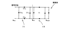
Next, an
具体的には誤差除去アダプタ30は、2ポートの散乱係数で表現される仮想上のアダプタであって次のように想定される。まず、実測測定治具誤差ET1,ET2の散乱係数行列が伝送行列に変換された上で、その伝送行列の逆行列が求められる。求められた逆行列が散乱係数行列に戻される。このような行列変換が実施されることで、誤差ET1 -1,ET2 -1を有する誤差除去アダプタ20が想定される。誤差除去アダプタ30の誤差ET1 -1,ET2 -1を実測することは不可能であるが、誤差ET1 -1,ET2 -1を上述したように想定することは可能である。
Specifically, the
図7に示されるように、試料DUT付きの実測測定治具5Bを実装した状態の誤差除去アダプタ30が実測測定装置2に接続され、その状態で試料DUTの特性が測定される状態が想定される。この場合、実測測定治具誤差ET1,ET2は誤差除去アダプタ20の誤差ET1 -1,ET2 -1によって相殺(除去)されることになる。したがって、その場合の試料DUTの測定値は試料真値S21DUT,S11DUTと見なされる。
As shown in FIG. 7, it is assumed that the
図8に示されるように、試料DUT付き実測測定治具5Bが実装された誤差除去治具アダプタ30が、さらに基準測定治具5Aに実装される状態が想定される。そしてこの状態の基準測定治具5Aが実測測定装置2に接続されて試料DUTの特性が測定される場合が想定される。このとき、誤差除去アダプタ30の入出力点における特性は、上述されたように試料真値S21DUT,S11DUTと見なされる。そのため、基準治具5Aの入出力点における特性は、基準治具測定値S21D,S11Dと見なされる。つまり、実測測定治具5Bと誤差除去アダプタ30と基準測定治具5Aとが順次実装された状態で試料DUTの特性が測定される状態は、図5に示された状況、すなわち、実測測定装置2に基準測定治具5Aが取り付けられた状態で試料DUTの特性が測定される状況と同一と見なされる。
As shown in FIG. 8, it is assumed that the error removing
以上の考察から、実測測定治具測定値S21T,S11Tに誤差除去アダプタ30の誤差ET1 -1,ET2 -1と基準測定治具誤差ED1,ED2とを掛け合わせれば、実測測定装置2における基準測定治具測定値S21D,S11Dを推定できることが理解される。
From the above consideration, test fixture measurement values S 21T, the error E T1 -1 of the
この推定を実現するためには、試料真値S21DUT,S11DUTと実測測定治具誤差ET1,ET2と基準測定治具誤差ED1,ED2と誤差除去アダプタの誤差ET1 -1,ET2 -1とが同定されることが条件となる。しかしながら、これらの値を同定することは不可能である。そのため、本発明では、次のような新たな状況が想定される。 In order to realize this estimation, the sample true values S 21DUT , S 11DUT , the actual measurement jig errors E T1, E T2 , the reference measurement jig errors E D1, E D2, and the error E T1 −1 , that the E T2 -1 is identified is a condition. However, it is not possible to identify these values. Therefore, in the present invention, the following new situation is assumed.
上述した図8に示される測定想定において、基準測定治具5Aと誤差除去アダプタ30とを合成することで、図9に示される単一のアダプタとすることが想定される。以下、上記合成により新たに想定されるアダプタが相対補正アダプタ31と称される。相対補正アダプタ31に起因して生じる誤差C1,C2は次のようにして算出される。基準測定治具誤差ED1,ED2と誤差除去アダプタ30の誤差ET1 -1,ET2 -1との散乱係数行列が伝送行列に変換されたうえでこれらの積が求められる。さらに求められる積が散乱係数行列に変換されることで、相対補正アダプタ31の誤差C1,C2が算出される。
In the measurement assumption shown in FIG. 8 described above, it is assumed that a single adapter shown in FIG. 9 is obtained by combining the
さらに、図9に示されるように、試料DUTが相対補正アダプタ31に実装され、さらに相対補正アダプタ31が実測測定治具5Bに実装される実装状態が想定される。さらにこのような実装形態において実測測定装置2が試料DUTの特定を測定する測定状態が想定される。このような測定状態で測定される測定値は基準測定治具測定値S21D,S11Dとなる。つまり、相対補正アダプタ31を想定すれば、基準測定治具5Aを用いることなく、実測測定治具5Bを用いても基準測定治具測定値S21D,S11Dを算定することができる。
Further, as shown in FIG. 9, it is assumed that the sample DUT is mounted on the
ここで、実測測定治具測定値S21T,S11Tと基準測定治具測定値S21D,S11Dとは、測定により得られる既知の値である。また、相対補正アダプタ31の誤差C1,C2を発生させる誤差要因(未知数)は有限数である。そのため、有限数の試料DUTを用いて、試料DUT(補正データ取得試料)の実測測定治具測定値S21T,S11Tと、基準測定治具測定値S21D,S11Dとが得られれば、相対補正アダプタ31に含まれる誤差要因を算定して前記誤差C1,C2を同定することができる。相対補正アダプタ31の誤差要因は種々の方法で算定することができる。次に相対補正アダプタ31の誤差要因の同定法の1例が説明される。
Here, the actual measurement jig measurement values S 21T and S 11T and the reference measurement jig measurement values S 21D and S 11D are known values obtained by measurement. The error factors (unknowns) that cause the errors C1 and C2 of the
本発明の補正アダプタ型相対補正法を実施するには、試料DUTとして、伝達係数が十分小さくほとんど無視し得る(好ましくはポート間伝達係数が−20dB以下の)特性を有する試料DUTが必要となる。 In order to carry out the correction adapter type relative correction method of the present invention, a sample DUT having a sufficiently small transfer coefficient and almost negligible (preferably a transfer coefficient between ports of -20 dB or less) is required as the sample DUT. .
ここで、試料DUTの伝達係数がどの程度小さくなければならないかについて検討する。測定治具の各ポートの補正アダプタを求める場合に、当該ポートにおける試料DUTの反射係数の測定値が他のポートの影響を受けていないことが望ましい。このとき、試料DUTの伝達係数が−AdBであったとすると、試料のあるポートに入射した測定信号は−AdB減衰して他のポートに伝達する。そして、前記他のポートに伝達した信号の一部は前記他のポートで反射され再び当該ポートに−Adb減衰して伝達する。この信号は、前記ポートにおける試料DUTの反射係数に重畳して誤差を生じる。例えば数GHz程度であれば、一般に前記他のポートで生じる反射は概ね−20dB程度であるから、試料DUTの伝達係数が−20dBあるとすれば、試料DUTへの入射信号に対して結局−60dB程度の信号が誤差信号になる。これは試料DUTへの入射信号の0.1%であり、この程度であればその影響は無視し得ることが多い。無論、ここで例に挙げた数値は必要な補正精度等によって変化するものであることはいうまでも無い。 Here, how small the transfer coefficient of the sample DUT must be examined. When obtaining a correction adapter for each port of the measurement jig, it is desirable that the measured value of the reflection coefficient of the sample DUT at that port is not affected by other ports. At this time, assuming that the transfer coefficient of the sample DUT is -AdB, the measurement signal incident on a certain port of the sample is attenuated by -AdB and transmitted to another port. Then, a part of the signal transmitted to the other port is reflected by the other port, and is again transmitted to the port with -Adb attenuation. This signal causes an error by being superimposed on the reflection coefficient of the sample DUT at the port. For example, if the transmission coefficient of the sample DUT is about -20 dB when the transmission coefficient of the sample DUT is about -20 dB when the reflection is generally about -20 dB when the frequency is about several GHz, -60 dB is eventually applied to the incident signal to the sample DUT. The degree signal becomes an error signal. This is 0.1% of the incident signal to the sample DUT, and the effect is often negligible at this level. Needless to say, the numerical values given in the examples here change depending on the required correction accuracy and the like.
補正アダプタ型相対補正法の説明に戻る。この状態が図10,図11に示される。図10は試料DUTが2ポートの場合の全体構成図であり、図11は、2ポートの試料DUTの1ポート拡大図である。以下の説明では、複数あるポートの中から任意の一ポートとしてポート1が説明に取り上げられる。
Return to the description of the correction adapter type relative correction method. This state is shown in FIGS. FIG. 10 is an overall configuration diagram when the sample DUT has two ports, and FIG. 11 is an enlarged view of one port of the two-port sample DUT. In the following description,
この場合、ポート(図10,図11ではポート1)からみて試料DUTは1ポートデバイスと見なされる。そのため、相対補正アダプタ31の誤差要因C100,C110,C111,C101は各ポート毎に独立に求められる。相対補正アダプタ31の誤差要因である順方向伝達係数C110と逆方向伝達係数C101とは相反定理により必ず等しくなる。したがって、一見、4つあるように見える相対補正アダプタ31の誤差要因は、詳細に見れば独立変数として3つ係数C100,(C110= C101),C111となる。そのため、3種類の試料DUTについて、実測測定治具測定値S21T,S11Tと、基準測定治具測定値S21D,S11Dとが得られれば、相対補正アダプタ31の誤差要因(伝達係数等)C100,(C110= C101),C111を同定することが可能となる。
In this case, the sample DUT is regarded as a one-port device as viewed from the port (
ポート1において、3個の試料DUT(補正データ取得試料11B)について測定した実測測定治具測定値S21T,S11Tと基準測定治具測定値S21D,S11Dとを用いた誤差補正アダプタ31の誤差要因の算定式は、次の(1)式となる。(1)式において、実測測定治具測定値S21T,S11Tや基準測定治具測定値S21D,S11Dの下付文字の末尾に付された番号1,2,3は、それぞれ特性を測定した3個の試料DUT(補正データ取得試料11B)の試料番号を示している。
In

ここで、C101(=C110)に含まれる符号(±Sqrt…の部分(Sqrtは平方根を意味する))を決定することは直接的には不可能である。これは、治具の電気長が物理的には半波長だけ長い(又は短い)場合には往復で位相が2π回転することから反射波だけを観察しても元の電気長と区別不可能である、という理由に因っている。しかしながら、伝達係数ではこの符号が重要になる場合があり、正しい符号を決定しなければならない。 Here, it is not directly possible to determine the sign (± Sqrt... (Sqrt means square root)) included in C1 01 (= C1 10 ). This is because if the electrical length of the jig is physically longer (or shorter) by half a wavelength, the phase will rotate by 2π in a reciprocating manner, so even if only the reflected wave is observed, it cannot be distinguished from the original electrical length. It is because there is. However, this sign may be important in the transfer coefficient, and the correct sign must be determined.
本発明が主に適用される数GHz程度の低い周波数では一般に波長は治具5A,5Bの電気長よりも長く、冶具5A,5Bのほうが波長の電気長より長い場合は正符号を、逆の場合には負符号を付せばよく、そのような場合においては特に問題なく、本発明の補正アダプタ型相対補正法が実施可能となる。
At a low frequency of about several GHz to which the present invention is mainly applied, the wavelength is generally longer than the electrical length of the
ポート2側の相対補正アダプタ31の誤差要因も上述したポート1側と同様に同定される。さらには、このようにして同定されるポート1,2の誤差要因を、次の(2)式に代入することで、実測測定治具測定値S21T,S11Tから基準測定治具測定値S21D,S11Dを推定することができる。
The error factor of the
次に、ポート数3以上の場合において、実測測定治具測定値S21T,S11Tから基準測定治具測定値S21D,S11Dを推定する補正方法が説明される。補正アダプタ型相対補正法の計算は、上述したように、実測測定治具測定値S21T,S11Tが既知定数となり、基準治具測定値S21D,S11Dが未知変数となる線形連立方程式に帰着する。線形連立方程式の元数はポート数×3である。この方程式を解くことで本発明の補正アダプタ型相対補正法が実現される。 Next, a description will be given of a correction method for estimating the reference measurement jig measurement values S 21D and S 11D from the actual measurement jig measurement values S 21T and S 11T when the number of ports is three or more. As described above, the correction adapter type relative correction method calculates a linear simultaneous equation in which the measured jig measured values S 21T and S 11T are known constants and the reference jig measured values S 21D and S 11D are unknown variables. Come back. The element number of the linear simultaneous equation is the number of ports × 3. By solving this equation, the correction adapter type relative correction method of the present invention is realized.
上記線形連立方程式は計算機アルゴリズムで容易に自動的に生成される。さらにこの連立方程式を、LU分解法(線形連立方程式の求解アルゴリズムの一つであっていわゆる直説法である)などの一般的方法で解くことにより、任意のポート数の測定系に対応した本発明の補正アダプタ型相対補正法が実現される。 The linear simultaneous equations are easily and automatically generated by a computer algorithm. Further, by solving this simultaneous equation by a general method such as an LU decomposition method (one of the algorithms for solving a linear simultaneous equation, which is a so-called straightforward method), the present invention corresponding to a measurement system with an arbitrary number of ports Is realized.
この方法は測定系のポート数を問わずに適用できるものの、計算時間が長くなる。処理の迅速性を高めるのであれば、線形連立方程式をあらかじめ代数的に解いておき、この式を用いて補正計算をすれば良い。ただし、この場合、任意のポート数の測定系に対応可能な汎用性は失われる。 Although this method can be applied irrespective of the number of ports of the measurement system, the calculation time becomes long. In order to enhance the speed of the processing, the simultaneous linear equations may be solved algebraically in advance, and the correction calculation may be performed using this equation. However, in this case, versatility that can support a measurement system with an arbitrary number of ports is lost.
実測測定治具測定値S21T,S11Tを未知変数とし、基準測定治具測定値S21D,S11Dを既知定数として上記線形連立方程式を解くことは、SOLT補正法における計算方法と等価である。これにより、本発明の補正アダプタ型相対補正法で、任意のポート数の測定系におけるSOLT補正が実施可能となる。以下、3ポート以上を対象とした補正アダプタ型相対補正法が説明される。 Solving the above-mentioned linear simultaneous equation using the actual measurement jig measurement values S 21T and S 11T as unknown variables and the reference measurement jig measurement values S 21D and S 11D as known constants is equivalent to the calculation method in the SOLT correction method. . This makes it possible to perform SOLT correction in a measurement system with an arbitrary number of ports by the correction adapter type relative correction method of the present invention. Hereinafter, a correction adapter type relative correction method for three or more ports will be described.
本発明の補正アダプタ型相対補正法においては、基準測定治具測定値S21D,S11Dは次のように求められる。基準測定治具測定値S21D,S11Dは、実測測定治具測定値S21T,S11Tとして表される測定モデルにおける各ポートに相対補正アダプタ31という一種の2ポート回路網を接続した場合の散乱係数として求められる。したがって、本発明の補正アダプタ型相対補正法は、実測測定治具測定値S21T,S11Tで表される測定モデルに相対補正アダプタ31を取り付けた状態の散乱係数を求める方法として規定される。
In the correction adapter type relative correction method of the present invention, the reference measurement jig measurement values S 21D and S 11D are obtained as follows. The reference measurement jig measurement values S 21D and S 11D are obtained by connecting a type of two-port network called a
以下、既に相対補正アダプタ31が得られているとして、実際に実測測定治具測定値S21T,S11Tから基準測定治具測定値ED1,ED2を計算する手順が説明される。なお、説明の都合上、2ポート測定系のモデルを用いて説明するが、任意のポート数の測定系について全く機械的に拡張できるのはいうまでもない。
The procedure for calculating the reference measurement jig measurement values E D1 and E D2 from the actually measured measurement jig measurement values S 21T and S 11T on the assumption that the
図12には、基準測定治具測定値S21D,S11Dで表される測定モデルの各ポートに相対補正アダプタ31を取り付けた状態の順方向シグナルフローダイアグラムが示される。図12は、図9の測定モデルをさらに詳細に規定した測定モデルである。
FIG. 12 shows a forward signal flow diagram in which the
図12において、ET1,ET2は、実測測定治具5Bの各ポートの誤差要因を示す2ポート回路網である。2ポート回路網ET1,ET2の誤差要因となる散乱係数は測定により求められない。C1 11,C1 12,C1 21,C1 22は、ポート1側の相対補正アダプタ31の誤差要因となる係数である。係数C1 11,C1 12,C1 21,C1 22は、計算により得られる。N1 1,N1 2,N1 3,N1 4は、ポート1側の相対補正アダプタ31の各ノードの値である。C2 11,C2 12,C2 21,C2 22は、ポート2側の相対補正アダプタ31の誤差要因となる係数である。係数C2 11,C2 12,C2 21,C2 22は、計算により得られる。N2 1,N2 2,N2 3,N2 4は、ポート2側の相対補正アダプタ31の各ノードの値である。S11DUT,S21DUTは試料DUTの散乱係数である。散乱係数S11DUT,S21DUTは測定により求められない。S11T,S21Tは実測測定治具測定値である。実測測定治具測定値S11T,S21Tは測定装置で測定される値である。S11D,S21Dは、補正アダプタ型相対補正法により推定される基準治具測定値である。
In FIG. 12, E T1 and E T2 are two-port networks showing error factors of each port of the
図12のシグナルフローダイアグラムにおいて、各ノードの値は隣接するノードからの信号入力の和である。また、この入力は隣接するノードの値と信号伝達経路の係数の積として与えられる。 In the signal flow diagram of FIG. 12, the value of each node is the sum of signal inputs from adjacent nodes. This input is given as the product of the value of the adjacent node and the coefficient of the signal transmission path.
図中のノードN1 3はノードN1 1とノードN1 4とから信号が入力される。また、これらノードN1 1,N1 4からノードN1 3に信号が伝播する間にそれぞれC1 11,C1 12倍される。したがって、ノードN1 3においては次の(3)式が成立する。
N1 3=C1 11N1 1+C1 12N1 4 …(3)
各ノードにおいても上記した関係がそれぞれ成立する。このような関係を整理すると、次の(4)式群が得られる。なお、(4)式群は各ポート毎に機械的に求めることができるので、計算機処理を行う際には任意のnポートについてこの関係式を算定することは容易である_Hlt34126945 (4)_Hlt34126945式群の左側に記した式はポート1に、右側に記した式はポート2に対応している。両者はポート番号を除き全く同じ式であり、さらにポート数が増えても計算機アルゴリズムで自動生成できる 。
Node N 1 3 in the figure signal is input from node N 1 1 and node N 1 4 Tokyo. The signal is C 1 11, C 1 12-fold, respectively while propagating from the nodes N 1 1, N 1 4 to node N 1 3. Therefore, the following equation (3) holds at the node N 1 3.
N 1 3 = C 1 11 N 1 1 +
The above-mentioned relationship is also established in each node. By rearranging such a relationship, the following equation (4) group is obtained. It should be noted that since equation group (4) can be obtained mechanically for each port, it is easy to calculate this relational expression for any n ports when performing computer processing. _Hlt34126945 (4) _Hlt34126945 The expression on the left side of the expression group corresponds to
N1 2=C1 21N1 1+C1 22N1 4 N2 2=C2 21N2 1+C2 22N2 4
N1 3=C1 11N1 1+C1 12N1 4 N2 3=C2 11N2 1+C2 12N2 4
N1 4=S11TN1 2+S12TN2 2 N2 4=S22TN2 2+S21TN1 2 …(4)
定数条件となる既知量が以下に説明される。順方向測定の場合には、ポート1側の信号源出力は1と見なされる。また、ポート2側の信号入力は0と見なされる。これより、以下に示す(5)式の条件が得られる。
N 1 2 = C 1 21 N 1 1 +
N 1 3 = C 1 11 N 1 1 +
N 1 4 = S 11T N 1 2 +
The known quantities that serve as constant conditions are described below. In the case of the forward measurement, the source output on the
また、求めたい未知数(基準測定治具測定値S21D,S11D)と各ノードとの間には、次の(6)式が成立する。 In addition, the following equation (6) is established between the unknowns to be obtained (reference measurement jig measurement values S 21D and S 11D ) and each node.
(4)式〜(6)式は線形連立方程式である。この線形連立方程式において未知数の数と方程式の数が一致している。そのため、これらの線形連立方程式を解くことによって未知数である基準測定治具測定値S11D,S21Dが求められる。計算機による線形連立方程式の解法はどんな物でも良いが、方程式の元数が大きくないのでLU分解法のような直接法により比較的簡単に解くことができる。 Equations (4) to (6) are linear simultaneous equations. In this linear simultaneous equation, the number of unknowns matches the number of equations. Therefore, the reference measurement jig measurement values S 11D and S 21D that are unknowns are obtained by solving these linear simultaneous equations. Although any method of solving a system of linear equations by a computer may be used, it can be relatively easily solved by a direct method such as the LU decomposition method since the equations are not large.
以上は、順方向の測定時における基準測定治具測定値S11D,S21Dの算定方法である。逆方向測定時における基準測定治具測定値S11D,S21Dは、定数条件と未知数の算定式である前記(5),(6)式に替えて、それぞれ(7)式と(8)式とを用いるだけであって、(4)式はそのまま用いられる。 The above is the calculation method of the reference measurement jig measurement values S 11D and S 21D at the time of forward measurement. The reference measurement jig measured values S 11D and S 21D at the time of the backward measurement are replaced by the above-mentioned equations (5) and (6), which are the equations for calculating the constant conditions and unknowns, respectively, by equations (7) and (8). And (4) is used as it is.
以上、2ポートの場合を例に挙げて説明したが、上記連立方程式を任意のnポートの場合に計算機アルゴリズムによって自動的に発生させてこれを解くことは容易であり、これによって任意のポート数の測定系について補正アダプタ型相対補正法が実施可能である。 As described above, the case of two ports has been described as an example. However, it is easy to automatically generate the above simultaneous equation by a computer algorithm in the case of an arbitrary n ports and solve the same, whereby the arbitrary number of ports can be obtained. The correction adapter type relative correction method can be implemented for the measurement system of (1).
上述した説明では、相対補正アダプタ31を実測測定治具測定値S21T,S11Tで表される測定モデルに取り付けた場合の散乱係数として基準測定治具測定値S21D,S11Dを求める方法について説明した。これは、数学的にいえば、実測測定治具測定値S21T,S11Tを既知定数と見なし、基準測定治具測定値S21D,S11Dを未知変数と見なしたうえで、前記(4)式を解いていることになる。
In the above description, a method of obtaining the reference measurement jig measurement values S 21D and S 11D as the scattering coefficient when the
これに対して、上記とは逆に、基準測定治具測定値S21D,S11Dを既知定数と見なし、実測測定治具測定値S21T,S11Tを未知変数と見なしたうえで、前記(4)式を解くことも可能である。この場合、実測測定治具測定値S21T,S11Tを試料DUTの真値と読み替え、基準測定治具測定値S21D,S11Dを測定装置の観測値と読み替えることで、測定装置の観測値から試料DUTの真値を求めることができる。これは、SOLT補正と全く同じ処理である。この場合、相対補正アダプタ31はSOLT補正の誤差モデルに対応するものとなる。
On the other hand, contrary to the above, the reference measurement jig measurement values S 21D and S 11D are regarded as known constants, and the actual measurement jig measurement values S 21T and S 11T are regarded as unknown variables. Equation (4) can also be solved. In this case, the actual measurement jig measurement values S 21T and S 11T are read as the true values of the sample DUT, and the reference measurement jig measurement values S 21D and S 11D are read as the observation values of the measurement device to obtain the observation values of the measurement device. From this, the true value of the sample DUT can be obtained. This is exactly the same processing as SOLT correction. In this case, the
上記解法に従い、前記(4)式に次の(9)式を適用した方程式と、前記(4)式に次の(10)式を適用した方程式とで表される連立方程式を解くことでSOLT補正が実施される。SOLT補正の実施により、未知数とされたS11T・S21T・S12T・S22Tが特定される。 According to the above solution, SOLT is obtained by solving a simultaneous equation expressed by the following equation (9) applied to the above equation (4) and the following equation (10) applied to the above equation (4). Correction is performed. The implementation of the SOLT calibration, S 11T · S 21T · S 12T · S 22T which are the unknowns are identified.
なお、S12T,S22Tは、図示はしていないがそれぞれ逆方向の伝達係数,反射係数の実測測定治具測定値を示している。これらは順方向測定のS21T,S22Tに対応する。 Although not shown, S 12T and S 22T indicate actual measurement jig measurement values of the transfer coefficient and the reflection coefficient, respectively, in the opposite directions. These correspond to S21T and S22T of the forward measurement.
前述したように、これら連立方程式はポート数を任意に設定した測定系おいて容易に計算機アルゴリズムで生成して解くことが可能である。これにより、任意のnポートにおいてSOLT補正を実行することが可能となる。 As described above, these simultaneous equations can be easily generated and solved by a computer algorithm in a measurement system in which the number of ports is arbitrarily set. This makes it possible to execute SOLT correction at an arbitrary n port.
なお、SOLT補正の誤差要因(散乱係数等)の求め方は次のようにすればよい。特性の異なる3種の試料DUTを用意し、各ポートそれぞれにおける3種の試料DUTの測定値を既知量とする。これにより、方向性・ソースマッチ・反射トラッキングの3つの誤差要因(誤差係数)を求めて1ポート補正する。さらに、1ポート補正が終わったポートで他のポートのロードマッチ・伝達トラッキングの2つの誤差要因(誤差係数)を求める。これにより、SOLT補正の誤差要因(散乱係数数)は求められる。 The error factor (scattering coefficient, etc.) of the SOLT correction may be obtained as follows. Three types of sample DUTs having different characteristics are prepared, and the measured values of the three types of sample DUTs at each port are set to known values. Thus, one-port correction is performed by obtaining three error factors (error coefficients) of directionality, source match, and reflection tracking. Further, two error factors (error coefficients) of load match and transmission tracking of the other port are obtained from the port for which the one-port correction has been completed. Thus, the error factor (the number of scattering coefficients) of the SOLT correction is obtained.
このような補正アダプタ型相対補正方法は、5ポート以上の測定系の補正を行う必要がある場合に有効となる。特に、平衡測定では不平衡ポートに換算した場合のポート数が非常に多くなることがあるので有用であると思われる。 Such a correction adapter type relative correction method is effective when it is necessary to correct a measurement system having five or more ports. In particular, it is considered useful in balanced measurement because the number of ports converted to unbalanced ports may be very large.
次に、本発明の補正アダプタ型相対補正法が、実際的に測定された結果が参照されながら説明される。主な測定条件は以下の通りである。
測定対象電子部品11A(試料DUT):不平衡入力-平行出力SAWフィルタ(fn=1842.5MHz)(SAFSD位G84CB0T00)であって、これら電子部品の良品(3個)と不良品(2個)とが測定対象電子部品11Aとして用意される。
補正データ取得試料11B:SMAコネクタに直接チップ部品がはんだ付けされる等の処理が施されることで略開放・略短絡・略終端が設定された3種の電子部品が補正データ取得試料11Bとして用意される。
基準測定治具5A:上記測定対象電子部品11A(試料DUT)が実装可能なKMM製の治具が基準測定治具5Aとして用意される。
実測測定治具5B:上記治具の校正面に誤差要因として、ポート1に50cmの同軸ケーブルが取り付けられ、ポート2に30mmのアダプタが取り付けられ、ポート3に−3dBの減衰器が取り付けられたものが実測測定治具5Bとして用意される。
基準測定装置1や実測測定装置2を構成する測定器:ADVANTEST社製 R3860 (〜8GHzの4ポートネットワークアナライザ)が測定器として用意される。上記基準測定治具5Aが接続された測定器が基準測定装置1となり、上記実測測定治具5Bが接続された測定器が実測測定装置2となる。
周波数範囲:1650MHz〜2050MHz
データ数:401点
IF帯域幅等:1000Hz(平均化処理無し)
測定方法:
1.上記基準測定治具5Aに3種の上記補正データ取得試料11Bがそれぞれ実装される。試料11B実装状態の基準測定治具5Aが上記測定装置に接続されてその特性が測定される。この場合、測定装置は基準測定装置1と見なされる。測定された特性が補正データ取得試料11Bの基準測定治具測定値S21D,S11Dと見なされる。
2.同様に、上記実測測定治具5Bに3種の上記補正データ取得試料11Bがそれぞれ実装される。試料11B実装状態の実測測定治具5Bが上記測定装置に接続されてその特性が測定される。この場合、測定装置は実測測定装置2と見なされる。測定された特性が補正データ取得試料11Bの実測測定治具測定値S21T,S11Tと見なされる。
3.補正データ取得試料11Bの測定結果である基準測定治具測定値S21D,S11Dと実測測定治具測定値S21T,S11Tとが、前述された(1)式に代入されることで、相対補正アダプタ31の誤差要因が算定される。
4.上記基準測定治具5Aに測定対象電子部品11Aがそれぞれ実装される。部品11A実装状態の基準測定治具5Aが上記測定装置に接続されてその特性が測定される。この場合、測定装置は基準測定装置1と見なされる。測定された特性が測定対象電子部品11Aの基準測定治具測定値S21D,S11Dと見なされる。
5.同様に、上記実測測定治具5Bに上記測定対象電子部品11Aがそれぞれ実装される。部品11A実装状態の実測測定治具5Bが上記測定装置に接続されてその特性が測定される。この場合、測定装置は実測測定装置2と見なされる。測定された特性が測定対象電子部品11Aの実測測定治具測定値S21T,S11Tと見なされる。
6.測定対象電子部品11Aの実測測定治具測定値S21T,S11Tが前述された(2)式に代入されることで、測定対象電子部品11Aの基準測定治具測定値S21D,S11Dが推定される。
Next, the correction adapter type relative correction method of the present invention will be described with reference to actually measured results. The main measurement conditions are as follows.
Measurement target
Correction
Measuring device constituting the
Frequency range: 1650MHz to 2050MHz
Number of data: 401 points IF bandwidth, etc .: 1000 Hz (no averaging process)
Measuring method:
1. The three types of correction
2. Similarly, the three types of correction
3. By substituting the reference measurement jig measurement values S 21D , S 11D and the actual measurement jig measurement values S 21T , S 11T which are the measurement results of the correction
4. The
5. Similarly, the
6. By substituting the actual measurement jig measurement values S 21T and S 11T of the measurement target
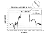
図13,図14に測定対象電子部品(良品)11Aの伝達係数(Sds21)の補正結果が示される。図13は1650MHz〜2050MHzの全体像を示し、図14は図13の要部拡大図である。これらの図において、Definitionは、基準測定治具測定値S21D,S11Dを示し、Testは実測測定治具測定値S21T,S11Tを示し、Correctedは、相対補正結果を示す。これらの図においては、Testが相対補正されることによってCorrectedに補正され、これがDefinitionと一致していれば良い、ということである。 13 and 14 show correction results of the transfer coefficient (Sds21) of the electronic component to be measured (non-defective product) 11A. FIG. 13 shows an overall image of 1650 MHz to 2050 MHz, and FIG. 14 is an enlarged view of a main part of FIG. In these figures, Definition is the standard test fixture measurement values S 21D, shows the S 11D, Test the test fixture measurement values S 21T, shows the S 11T, the Corrected shows the relative correction result. In these figures, Test is corrected to Corrected by relative correction, and it is only necessary that this is equal to Definition.
これらの図を詳細に検討すれば明らかなように、実測測定治具測定値S21T,S11Tは治具間誤差の相違の影響で基準測定治具測定値S21D,S11Dと大きく異なる結果となっている。しかしながら、実測測定治具測定値S21T,S11Tが本発明の相対アダプタ型相対補正法により補正された結果は、ほぼ正確に基準測定治具測定値S21D,S11Dに一致している。つまり、本願発明の補正アダプタ型相対補正法を実施することにより、正確に補正されていることが分かる。 As is clear from a detailed examination of these figures, the actual measurement jig measurement values S 21T and S 11T are significantly different from the reference measurement jig measurement values S 21D and S 11D due to the difference between the jigs. It has become. However, test fixture measurement values S 21T, results S 11T is corrected by the relative adapter type relative correction method of the present invention, almost exactly the standard test fixture measurement values S 21D, are matched to the S 11D. That is, it is understood that the correction is accurately performed by performing the correction adapter type relative correction method of the present invention.
図15,図16に測定対象電子部品(不良品)11Aの伝達係数(Sds21)の補正結果が示される。図15は1650MHz〜2050MHzの全体像を示し、図16は図15の要部拡大図である。本発明の補正アダプタ型相対補正法は試料特性の線形性が保たれる限り、試料の特性に関係無く補正を実施できる。したがって、測定対象電子部品(不良品)11Aについても精度の高い補正が実施されている。なお、これらの図において、Definition,Test,Correctedは、図13,図14で説明したものと同様のものを示す。 15 and 16 show correction results of the transfer coefficient (Sds21) of the electronic component to be measured (defective product) 11A. FIG. 15 shows an overall image of 1650 MHz to 2050 MHz, and FIG. 16 is an enlarged view of a main part of FIG. The correction adapter type relative correction method of the present invention can perform correction regardless of the characteristics of the sample as long as the linearity of the characteristics of the sample is maintained. Therefore, highly accurate correction is also performed for the electronic component to be measured (defective product) 11A. In these figures, Definition, Test, and Corrected are the same as those described in FIG. 13 and FIG.
図17に測定対象電子部品(良品)11Aの通過域付近における一方の不平衡伝達係数(Sss31)の補正結果が示される。補正結果は極座標表示で示される。平衡ポートには2つの不平衡ポートの差動信号が入力される。そのため、振幅が正しく補正されているだけでは正常な平衡ポートの補正は期待できない。振幅と同時に位相も正しく補正されていることが必要である。 FIG. 17 shows a correction result of one unbalanced transfer coefficient (Sss31) in the vicinity of the pass band of the electronic component to be measured (non-defective product) 11A. The correction result is shown in polar coordinates. Differential signals of two unbalanced ports are input to the balanced port. Therefore, correct correction of a normal balanced port cannot be expected only by correcting the amplitude correctly. It is necessary that the phase as well as the amplitude are correctly corrected.
これに対して、図17は、ポート3に減衰器を挿入したことにより、実測測定治具測定値S21T,S11Tは、基準測定治具測定値S21D,S11Dに対して振幅が大きく減衰(3dB減衰しているはずである)していると共に、その電気長によって位相が回転している。これに対して、補正結果は振幅・位相とも正常に再現されている。
On the other hand, FIG. 17 shows that the actual measurement jig measurement values S 21T and S 11T have a larger amplitude than the reference measurement jig measurement values S 21D and S 11D due to the insertion of the attenuator in
図18に、測定対象電子部品(良品)11Aの通過域付近の反射係数(Sss33)の補正結果が示される。反射係数に関しても、本発明の補正アダプタ型相対補正法を実施すれば良好な補正結果が得られる。 FIG. 18 shows a correction result of the reflection coefficient (Sss33) near the pass band of the electronic component to be measured (non-defective product) 11A. Regarding the reflection coefficient, a good correction result can be obtained by performing the correction adapter type relative correction method of the present invention.
次に、本発明の補正アダプタ型相対補正法に用いる補正データ取得試料11Bが説明される。
Next, the correction
本発明の補正アダプタ型相対補正法を実施するためには、ポート間の伝達係数が0に限りなく近い(好ましくは、ポート間伝達係数が−20dB以下)特性を有する補正データ取得試料11Bが必要となる。そのような補正データ取得試料11Bを構成するためには、補正データ取得試料11Bのポート間絶縁をできる限り高くする必要がある。ポート間絶縁を高めるためにはポート間にシールドを設けることも考えられるが、構成が複雑化してコストアップを招く。
In order to carry out the correction adapter type relative correction method of the present invention, a correction
ここで、静電結合や誘電結合が強い素子から補正データ取得試料11Bを構成する場合、ポート間の漏洩を多く生じる伝送モードは試料11Bの形状によって決まる。そのため、例えば、誘導結合が強い素子から補正データ取得試料11Bを構成する場合には次のような特性が得られる。すなわち、両方のポートとも短絡状態にすると、その両ポート間の絶縁性は非常に低くなる。一方のポートを短絡状態にし他方のポートを開放状態にすれば、開放側ポートが磁気結合しないので、両ポート間の絶縁特性は高く保持される。したがって、図19(a),(b)に示されるように、3個必要となる補正データ取得試料11Bの一方を、(開放・短絡)の構成とし、他方を(短絡・開放)の構成とすればよい。そうすれば、従来実施されていた(開放・開放+短絡・短絡)という組合せと同様に、(開放・短絡+短絡・開放)という組合せを使うことが可能となる。これにより、補正手順に影響を与えることなく、本発明の補正アダプタ型相対補正法が実施可能となる。
Here, when the correction
補正データ取得試料11Bとして終端(50Ω)を使う場合も同様である。この場合、(終端・終端)の構成にすると絶縁性が低下する場合がある。これに対して、(終端・開放)の構成にすれば、両ポート間の絶縁特性を高く保持することができる。したがって、図19(c),(d)に示されるように、3個必要となる補正データ取得試料11Bの一方を、(開放・終端)の構成とし、他方を(終端・開放)の構成とすればよい。そうすれば、従来実施されていた(開放・開放+終端・終端)という組合せと同様に、(開放・終端+終端・開放)という組合せを使うことが可能となる。これにより、補正手順に影響を与えることなく、補正アダプタ型相対補正法が実施可能となる。ただし、この場合、補正データ取得試料11Bとして必要な個数は、1つ増えて4個となる。開放は、すでに他の補正データ取得試料11Bで測定が完了しているので、そのデータは捨てられることになる。終端以外の反射端(例えば100Ωや10Ω等)を用いる場合も、同様となる。
The same applies to the case where the termination (50Ω) is used as the correction
多層構造を有する電子部品(LTCCデバイス等)から補正データ取得試料11Bを構成する場合、開放,短絡は容易に製作できても終端(50Ω)等を製作することは困難である。
When the correction
その場合には、終端形成に必要な抵抗素子の代わりにディレイラインを用いることができる。この場合、ディレイラインの末端は、開放端でも短絡端でもよい。ただし、この場合、挿入されるディレイラインによって、補正データ取得試料11Bの反射波の位相が相互にほぼ均等にずれるように設計することが望ましい。そうすれば、補正データ取得試料11B相互の特性が離間する結果、測定誤差の影響をさらに受けにくくなる。具体的には、開放,短絡とともに必要となる場合には、90°位相と、270°位相のディレイラインを設けるのが好ましい。これは、開放は0°、短絡は180°の位相を有する為である。3種類のディレイラインが必要となる場合には、0°(=開放)位相のディレイラインと,120°位相のディレイラインと,240°位相のディレイラインとを設けるのが最適である。
In that case, a delay line can be used instead of the resistance element necessary for the termination formation. In this case, the end of the delay line may be an open end or a short-circuit end. However, in this case, it is desirable to design so that the phases of the reflected waves of the correction
ディレイラインは、導体パターンだけ形成できる。そのため、ディレイラインを有する補正データ取得試料11BがLTCCデバイス(低温焼成セラミックスを用いたデバイス)として容易に実現可能である。これに対して、終端(50Ω)のように抵抗体を必要とする補正データ取得試料11BをLTCCデバイスで実現するのは困難であるか、実現できたとても高コストとなる。
The delay line can be formed only of the conductor pattern. Therefore, the correction
2ポート以上の補正データ取得試料11Bの各ポートにディレイラインを設ける場合には、絶縁性が低下することがある。この場合には、1ポートをディレイラインにしたうえで、他のポートを開放にする、短絡にする、といった構成にすることで、絶縁性の低下を阻止することができる。
When a delay line is provided for each port of the correction
上記のように補正データ取得試料11Bを構成すれば、ポート間の伝達係数が非常に小さくなる結果、ポート間のアイソレーションが高い補正データ取得試料11Bが獲得できる。したがって、本発明の補正アダプタ型相対補正方法の補正精度が高くなる。
If the correction
また、開放端では電流は全く流れない代わりに電圧の変動が生じる。そのため、開放端から短絡端へ向かって電界波が生じる。ところが、短絡端では電流は流れることができる(磁界波は受信する)ものの電圧の変動は生じ得ない(電界波は受信しない)。したがって、結局のところ、ポート間の結合が生じず、高いアイソレーションが得られる。逆の構成でも同様の効果が得られる。 Further, at the open end, no current flows at all, but voltage fluctuation occurs. Therefore, an electric field wave is generated from the open end to the short-circuit end. However, at the short-circuited end, a current can flow (a magnetic field wave is received) but a voltage cannot be changed (an electric field wave is not received). Therefore, after all, coupling between ports does not occur, and high isolation is obtained. A similar effect can be obtained with the reverse configuration.
終端とは、通常50Ωであってその他端には電界波・磁界波の両方が伝わる。この場合、補正データ取得試料11Bの構造によって電界波の影響が大きい場合には他端を短絡端に、磁界波の影響が大きい場合には他端を開放端にすればよい。そうすれば、ポート間の伝達係数を最も小さくすることができる。このことは、50Ω以外の終端を構成する場合も同様である。
The terminating end is usually 50Ω, and both electric and magnetic waves are transmitted to the other end. In this case, if the influence of the electric field wave is large due to the structure of the correction
ただし、例えば、終端・開放という構成を有する補正データ取得試料11Bを作製した場合、別の補正データ取得試料11Bとして短絡・開放という構成を備えたものを作製する場合、ポート2側について考察すると、開放という特性を有する補正データ取得試料11Bが2つ配置されることになる。これでは相対補正を正常に行えない。その場合、別に開放・終端という構成を有する補正データ取得試料11Bを作製すればよい。そうすれば、この補正データ取得試料11Bによるポート2の測定データでもってデータの重複を防ぐことができる。このことは、3ポート以上の場合も同様である。
However, for example, when the correction
次に、実施形態の変形例について説明する。この変形例は、測定対象(能動)電子部品であるバイポーラトランジスタをいわゆるエミッタ接地増幅回路で使用した場合の増幅度を測定する場合に、精度高く測定結果を補正する方法である。 Next, a modified example of the embodiment will be described. This modification is a method of correcting the measurement result with high accuracy when measuring the amplification when a bipolar transistor as a measurement target (active) electronic component is used in a so-called common emitter amplifier circuit.
図20は本変形例の実測測定治具5B’と基準測定治具5A’の構成を示す回路図である。図20には測定対象(能動)電子部品であるバイポーラトランジスタ50も図示される。実測測定治具5B’と基準測定治具5A’とは、バイポーラトランジスタ50を駆動する為に直流電圧を与える回路51と、バイポーラトランジスタ50に合わせてインピーダンス整合を行う回路52、外部回路と直流電圧を遮断し、交流信号のみを通す結合回路53などの電子部品が設けられている。この変形例では、バイポーラトランジスタ50を駆動する為に直流電圧を与える回路51により、直流電源が構成されている。
FIG. 20 is a circuit diagram showing the configuration of the
測定は、図示しない測定装置(ネットワークアナライザ等)1,2に設けられた接続用の同軸ケーブル4A,4Bを治具5A,5Bの各ポートに接続して行われる。図21は補正データ取得試料11B’の構成を示す回路図である。図21(a)は、短絡の試料11B’であり、図21(b)は、終端の試料11B’であり、図21(c)は、開放の試料11B’である。補正データ取得試料11B’は測定対象(能動)電子部品と同様に実測測定治具5B’や基準測定治具5A’に取り付け可能な形状に製作されている。
The measurement is performed by connecting the
以下、上記の構成における本変形例の誤差の補正方法について説明する。基準測定治具5A’と実測測定治具5B’とにそれぞれ計3個の同一の補正データ取得試料11B’が実装された状態で、各補正データ取得試料11B’の電気特性の基準測定治具測定値S21D,S11Dと実測測定治具測定値S21T,S11Tとが取得される。測定時、各補正データ取得試料11B’には、直流電圧付与回路51によって同一レベルの直流電圧が印加されるように制御されており、各補正データ取得試料11B’の電気特性の基準測定治具測定値S21D,S11Dと実測測定治具測定値S21T,S11Tとは、この状態で測定される。なお、直流電圧付与回路51に替えて直流電流付与回路を設け、測定時、各補正データ取得試料11B’に、直流電流付与回路によって同一レベルの直流電流が付与されるように制御してもよい。この場合、直流電流付与回路により直流電源が構成される。また、直流電圧付与回路51といった直流電源は、上述したように、治具回路に組み込まれる以外に、治具外部(例えば、測定装置1,2)に設けられてもよい。
Hereinafter, a method of correcting an error of the present modification in the above configuration will be described. With a total of three identical correction
これら基準測定治具測定値S21D,S11Dと、実測測定治具測定値S21T,S11Tとから、相対補正アダプタ31が同定される。相対補正アダプタ31は、実測測定治具測定値S21T,S11Tから基準測定治具測定値S21D,S11Dを推定するアダプタであって、前述した実施の形態の補正方法によって同定される。その後、測定対象(能動)電子部品11A’が実測測定治具5B’に実装された状態でその電気特性が測定される。その際、各測定対象(能動)電子部品11A’には、直流電圧付与回路51によって同一レベルの直流電圧が印加されるように制御される。
These standard test fixture measurement values S 21D, and S 11D, test fixture measurement values S 21T, and a S 11T, the
得られた実測測定治具測定値S21T,S11Tと相対補正アダプタ31とから、測定対象(能動)電子部品11A’の基準測定治具測定値S21D,S11Dが算定される。具体的な実験条件は以下の通りである。
・測定対象(能動)電子部品:低周波小信号用汎用NPNトランジスタ(品番2SC1815:東芝製)
・測定周波数:1MHz〜3MHz
・測定器:8753ES(Agilent Technologies社製)
・信号源出力:−15dBm
・治具:図20の回路構成を有する基準測定治具5A’・実測測定治具5B’が使用される。ただし、基準測定治具5A’はできるだけ大きなゲインが得られるように回路が調整された状態(図中のchokeコイル と整合回路62のコンデンサを調整)とされる。一方、実測測定治具5B’は回路調整を上記の状態から適当にずらされる(コイル幅を少し広げてL値を下げ、コンデンサも少し容量をずらす)ことで、多少ゲインが少なくなるように調整された状態とされる。
・補正データ取得試料:図21に示されるように、3種類の3端子型の補正データ取得試料11B’が使用される。
・補正方法:図20に示されるように、測定対象(能動)電子部品11A’は、エミッタが直接接地された構成とされていることから、本発明の補正方法のうち、2ポートの測定対象電子部品に対する相対補正法が使用される。
The resulting test fixture measurement values S 21T, from S 11T and the relative correction adapter 31., standard test fixture measurement values S 21D of the measurement target (active)
・ Measurement target (active) electronic parts: General-purpose NPN transistor for low frequency small signal (Part No. 2SC1815: manufactured by Toshiba)
・ Measurement frequency: 1MHz-3MHz
-Measuring instrument: 8753ES (manufactured by Agilent Technologies)
・ Signal source output: -15dBm
Jig:
Correction data acquisition sample: As shown in FIG. 21, three types of three-terminal correction
Correction method: As shown in FIG. 20, the measurement target (active)
図22に順方向伝達係数(いわゆるゲイン)の基準測定治具測定値S21D(Definition)、実測測定治具測定値S21T(Test)、および補正結果(Corrected)が示される。実測測定治具測定値S21T,S11Tでは、基準測定治具測定値S21D,S11Dよりも約0.5dBほどゲインが低くなっているが、相対補正によってこの差は正しく補正されていることが分かる。 FIG. 22 shows a reference measurement jig measurement value S 21D (Definition), an actual measurement jig measurement value S 21T (Test), and a correction result (Corrected) of the forward transfer coefficient (so-called gain). Test fixture measurement values S 21T, the S 11T, the standard test fixture measurement values S 21D, but gain approximately 0.5dB than S 11D is low, this difference by the relative correction is corrected properly You can see that.
図23に、順方向伝達係数の極座標表示が示される。補正が位相も含めて正常に行えていることが読み取れる。なお、図22,図23において、Definition,Test,Correctedは、図13,図14で説明したものと同様のものを示す。 FIG. 23 shows a polar coordinate display of the forward transfer coefficient. It can be seen that the correction is normally performed including the phase. 22 and 23, Definition, Test, and Corrected are the same as those described with reference to FIGS.
このように、本変形例によれば、バイポーラトランジスタやFET、及びこれらを含む増幅器等の能動電子部品においても、実測測定治具測定値S21Tを、基準測定治具測定値S21Dに精度高く一致させることが可能となる。そのため、熟練者であっても長時間を要する非常に難易度の高い作業である実測測定治具5B’の調整作業などを行わなくとも、実測測定治具測定値S21Tから基準測定治具測定値S21Dを精度高く推定することが可能となる。これにより、治具調整作業が不要になるばかりか、治具調整作業を行ってもなお完全に基準測定治具測定値S21Dに一致する測定結果が得られないために従来では必要になっていた量産工程での良否判定閾値とユーザー保証値との間の余裕を設ける必要がなくなり、その分、良品率が向上する。
As described above, according to the present modification, even in active electronic components such as bipolar transistors and FETs and amplifiers including the same, the measured measurement jig measured value S21T is accurately converted to the reference measurement jig measured value S21D. It becomes possible to make them coincide. Therefore, even if the skilled person does not have to perform the adjustment work of the
次に、本変形例が、測定対象(能動)電子部品の測定値を精度高く補正できる理由を説明する。説明の都合上、バイポーラトランジスタのエミッタ接地増幅回路を例にとるが、バイポーラトランジスタはFETと並んで半導体増幅素子のもっとも基本的な構成要素であり、これの測定に適用できる測定法であれば、これらを含む他の複雑な能動電子部品の測定にも適用できることは明らかである。 Next, the reason why the present modified example can accurately correct the measured value of the measurement target (active) electronic component will be described. For convenience of explanation, a grounded-emitter amplifier circuit of a bipolar transistor is taken as an example.Bipolar transistors are the most basic constituent elements of a semiconductor amplifier alongside FETs. Obviously, it can be applied to the measurement of other complicated active electronic components including these.
バイポーラトランジスタを用いたもっとも基本的な増幅回路であるエミッタ接地増幅回路として図24に示されるものがある。測定対象(能動)電子部品(試料)であるバイポーラトランジスタ60は交流信号の増幅作用を有するが、バイポーラトランジスタ60を駆動する為に直流電圧を与える回路61やバイポーラトランジスタ60に合わせてインピーダンス整合を行う回路62、外部回路と直流電圧を遮断し、交流信号のみを通す結合回路63などの電子部品が設けられている。これらは全て前述した基準測定治具5A’,実測測定治具5B’間の測定値差の原因になる。
FIG. 24 shows a common emitter amplifier circuit which is the most basic amplifier circuit using bipolar transistors. The
直流電源は交流的には接地と等価であることを考慮に入れて図24の回路を交流的に書き直したのが図25である。図25の構成においては、バイアス抵抗は交流的なインピーダンスも有していることに注意が必要となる。図25中、伝送路に直列接続の素子、シャント接続の素子は全て散乱係数として合成できるので、ポート1側の素子群及び伝送路の誤差の散乱係数E1、ポート2側の素子群及び伝送路の誤差の散乱係数をE2、バイポーラトランジスタ60の散乱係数をSAとすると、図25の回路構成は、結局図26に示されるシグナルフローダイアグラムとなる。これは、単純な2ポート受動デバイス測定時のシグナルフローダイアグラムと同じものである。従って、以下に説明される6点に注意すれば受動デバイスの場合と全く同様に増幅素子についても本発明の相対補正法を適用することができる。
FIG. 25 is a diagram in which the circuit of FIG. 24 is rewritten in an AC manner in consideration of the fact that the DC power supply is equivalent to the ground in an AC manner. It should be noted that in the configuration of FIG. 25, the bias resistor also has an alternating impedance. In FIG. 25, the elements connected in series and the elements connected in shunt to the transmission line can all be synthesized as scattering coefficients, so that the element group on the
1.基準測定治具5A’と実測測定治具5B’との間で、DCバイアス状態をほぼ等しくする。
1. The DC bias state is made substantially equal between the
これは、測定対象(能動)電子部品11A’である増幅素子の真値や、基準測定治具5A’,実測測定治具5B’を構成する治具回路の特性が変化してしまうことを避ける為に必要な要件である。入出力インピーダンスの整合に使用されるようなコンデンサやインダクタは多くの場合、DC電圧依存性を持たないものが使用されると期待できるが、電源バイパス用に高誘電率セラミックコンデンサ等が使われる場合もあり得る。また、バイアス電圧安定化の為にダイオード等の半導体素子が使われる可能性もあり、これらは与えるDCバイアスによって高周波特性が変化してしまう。そのため、実際の測定対象(能動)電子部品11A’の測定時と同じ電源電圧を与えて、基準測定治具実装状態での測定時と実測測定治具実装状態での測定時との間で治具の特性が異なってしまうことを防がなければならない。本条件は、電源装置にいわゆる直流安定化電源を用いることで容易に実現できる。
This avoids a change in the true value of the amplifying element which is the measurement target (active)
2.実測測定治具や基準測定治具へのDC電圧入力部に十分なバイパスを施す。 2. Provide sufficient bypass to the DC voltage input to the actual measurement jig and the reference measurement jig.
増幅素子にDCバイアスを与える回路も当然ある程度の交流信号が漏洩する。交流電流の漏洩が大きいと、DC電源から治具5A’,5B’への電線の引き回しによって測定結果が変動するという事態に陥る可能性がある。したがって、治具5A’,5B’へのDC電圧入力部では十分なバイパスコンデンサを設けるなどして交流信号がDC系回路を通じて治具外に漏洩しないようにする。もっとも、これは本発明の補正法に関係なく、DC系の配線を手で触ると測定値が変わるなどという測定の再現性上の問題を引き起こすものであって、本質的には本発明とは無関係であるものの、必要となる要件である。
A circuit that applies a DC bias to the amplifying element naturally leaks some AC signal. If the leakage of the alternating current is large, there is a possibility that the measurement result may fluctuate due to the routing of the electric wires from the DC power supply to the
3.治具5A’,5B’間の特性差異が大きすぎるとダイナミックレンジが狭くなるため、治具5A’,5B’間の特性差異はできるだけ小さくする。
3. If the characteristic difference between the
交流的治具特性の差異の影響は原理的には相対補正法によって補正される。しかしながら、増幅素子の測定回路によっては共振周波数付近では非常に増幅度が高く、それ以外では非常に増幅度が低くなる場合がある。この例では、治具5A’,5B’間であまりに共振周波数がずれていると、非常に低い増幅度しか得られていない実測測定治具測定値S21T,S11Tから基準治具測定値S21D,S11Dの高い増幅度を推定することになり、ダイナミックレンジが不足することが懸念される。この様な場合は、大まかに治具5A’,5B’の特性を調整して大体の共振周波数を合わせておき、合わせきれない部分は補正アダプタ型相対補正法に任せる、という運用が考えられる。
In principle, the influence of the difference in the AC jig characteristics is corrected by the relative correction method. However, depending on the measurement circuit of the amplifying element, the amplification may be very high near the resonance frequency, and may be very low in other cases. In this example, if the resonance frequency is too deviated between the
4.補正用データ取得試料の入力ポートはAC結合する。 4. The input port of the correction data acquisition sample is AC-coupled.
補正用データ取得試料11B’の特性測定時の治具特性と測定対象(能動)電子部品11A’の特性測定時の治具特性とを等しくするために、補正データ取得試料11B’の特性測定時も電圧を印加すべきであるが、補正データ取得試料11B’として直流的短絡試料を設定して、この試料を治具5A’,5B’に実装するとDCバイアス状態が変化する可能性がある。そのため、補正データ取得試料11B’のポートはDCを阻止すべきである、という要件である。
In order to make the jig characteristic of the correction
5.測定対象(能動)電子部品11B’が増幅素子(回路)である場合、増幅素子は線形動作していなければならない。
5. When the measurement target (active)
信号レベルが大きすぎて増幅素子が飽和したり、あるいは回路の電源電圧にかかって出力がクリップしたりする場合は、回路動作は非線型動作になる。非線型動作時の特性は線形的な補正法である相対補正法で補正等できる見込みは無い。そのため、測定対象(能動)電子部品11B’が増幅素子(回路)である場合、増幅素子はいわゆる小信号応答のようにその回路動作が線形的(A級動作)を期待できる状態でなければならない、という要件である。
If the signal level is too high and the amplifier element is saturated, or if the output is clipped due to the power supply voltage of the circuit, the circuit operation will be non-linear. It is unlikely that the characteristics during the non-linear operation can be corrected by the relative correction method, which is a linear correction method. Therefore, when the measurement target (active)
6.複雑なデバイスではポート数が非常に多くなってしまう。 6. For complex devices, the number of ports can be very large.
増幅回路を構成する測定対象(能動)電子部品11B’としては、しばしば、働きは単純な電力増幅素子であっても、内部は多段の増幅器になっており、それぞれの増幅段に別々に電源を供給しなければならないようなデバイスがある。このようなデバイスの場合、厳密には、全ての電源端子の応答を観測しなければ完全な補正アダプタ型相対補正法を実施できず、そのために、非常に測定ポート数が増えてしまうという不具合が生じる。これについては、通常の増幅回路では出力に影響する電源ラインは限られているので、影響を無視し得るポートは無視すれば良い。例えば、通常の増幅器ではまず電圧増幅段が設けられ、次に1〜2段の電力増幅段が設けられる。この様な構成では、治具5A’,5B’によって測定結果が異なる原因となる電源ラインは第1段の電圧増幅段であることがほとんどである。そのため、このようなデバイスの測定結果を補正する際には、電源ラインのみを補正対象とし、他の電源ラインは無視すれば良い。
As a measurement target (active)
なお、測定対象(能動)電子部品11A’に設けられる接続端子の少なくとも一つが、直接、治具5A’,5B’の接地電位に接続される、あるいは治具5A’,5B’の少なくとも交流的に接地電位に接続される場合においては、補正データ取得試料11B’として、上述した接地電位を基準として各種の電気特性を有するものを容易に製作することができる。しかしながら、測定対象(能動)電子部品11A’のどの接続端子も接地電位に接続されず、治具5A’,5B’上で接地電位との間に何らかの電子部品が設けられる場合には、補正データ取得試料11B’を作製する際において、設定する電気特性の基準となる測定対象(能動)電子部品11A’の接地電位を定めることができない。この場合には、補正データ取得試料11B’を実現することが不可能となる。
Note that at least one of the connection terminals provided on the measurement target (active)
この様な場合には、
・基準測定治具5A’と実測測定治具5B’として、補正データ取得試料11B’と測定対象(能動)電子部品11A’とが有する各ポートに対応する接続端子以外に、各治具5A’,5B’の接地電位に接続される少なくとも一つの接地接続端子を有するものを用意する、
・補正データ取得試料11B’として、治具5A’,5B’に設ける接地接続端子に接続される端子を有するものを少なくととも一つ用意する、
・上記端子を有する補正データ取得試料11B’の実測測定治具測定値S21T,S11Tを取得する工程において、この補正データ取得試料11B’の電気特性を、上記端子(補正データ取得試料11B’)を接地接続端子(治具5A’,5B’)に接続した状態で測定する、
という工程をさらに加えればよい。
In such a case,
As the
-As the correction
In the step of acquiring the actual measurement jig measurement values S 21T and S 11T of the correction
What is necessary is just to add the process of further.
そうすれば、基準測定治具5A’と実測測定治具5B’を構成する治具回路上で接地電位との間に何らかの電子部品が設けられる場合であっても、補正データ取得試料11B’を実現することで可能となる。これにより、本発明の相対補正法を実施することができる。なお、接地接続端子は、治具回路の接地電位に接続されていることが望ましい。
Then, even if some electronic components are provided between the
以上説明した実施の形態では、測定対象電子部品11Aを実測測定治具5Bに実装した状態で実測測定装置2で測定した測定結果を、測定対象電子部品11Aを基準測定治具5Aに実装した状態で基準測定装置1で測定した測定結果に補正する際に本発明を実施する場合が説明された。ここで、基準測定装置1は、同一測定対象電子部品の電気特性の測定結果が実測測定装置2とは異なる測定装置の一例として規定される装置である。しかしながら、本発明はこの他、測定対象電子部品11Aを実測測定治具5Bに実装した状態で実測測定装置2で測定した測定結果を、測定対象電子部品11Aを基準測定治具5Aに実装した状態で実測測定装置2で測定した測定結果に補正する際においても本発明は同様に実施される。
In the embodiment described above, the measurement result measured by the
1 基準測定装置
2 実測測定装置
3A,3B ネットワークアナライザ
4A,4B,4C 同軸ケーブル
5A 基準測定治具
5B 実測測定治具
6 同軸ケーブルコネクタ
7 絶縁基板
7A 基板表面
8A,8B 信号伝送路
8C〜8i接地線路
9A,9B,9C 同軸コネクタ
10 スルーホール接続部
11A 測定対象電子部品
11B 補正データ取得試料
11a 基板裏面
12a,12b 伝送路端子
12C〜12f 接地端子
13 枠体
20 ネットワークアナライザ本体
21 制御部
22 制御部本体
23 メモリ
24 誤差要因同定手段
25 補正算定手段
30 誤差除去アダプタ
31 相対補正アダプタ
S11 順方向反射係数
S21 順方向伝達係数
S12 逆方向伝達係数
S22 逆方向反射係数
S21DUT,S11DUT 試料真値
S21D,S11D 基準測定治具測定値
S21T,S11T 実測測定治具測定値
ED1,ED2 基準測定治具誤差
ET1,ET2 実測測定治具誤差
ET1 -1,ET2 -1 第1誤差除去アダプタの誤差
C1,C2 相対補正アダプタの誤差
1
12a, 12b Transmission path terminals 12C to
Claims (18)
互いに異なる電気特性を有するとともに、各ポート間の伝達係数が極めて小さい補正データ取得試料を少なくとも3個用意する工程と、
前記補正データ取得試料の電気特性を基準測定治具実装状態で前記測定装置もしくは前記他の測定装置で測定することで、前記補正データ取得試料の基準測定治具測定値を取得する工程と、
前記補正データ取得試料の電気特性を実測測定治具実装状態で前記測定装置もしくは前記他の測定装置で測定することで、前記補正データ取得試料の実測測定治具測定値を取得する工程と、
前記実測測定治具の前記測定装置側に位置する各ポートに接続される2ポート回路網からなり、測定対象電子部品実装状態の前記実測測定治具が発生させる電気特性を測定対象電子部品実装状態の前記基準測定治具が発生させる電気特性に変更する特性を有する相対補正アダプタを想定したうえで、想定した相対補正アダプタの誤差要因を、前記補正データ取得試料の前記基準測定治具測定値および前記実測測定治具測定値から同定する工程と、
前記測定対象電子部品を前記実測測定治具に実装した状態で前記測定装置もしくは前記他の測定装置で測定することで、前記測定対象電子部品の実測測定治具測定値を取得する工程と、
前記測定対象電子部品の実測測定治具測定値を前記相対補正アダプタの誤差要因で補正することで、前記測定対象電子部品を前記基準測定治具に実装した状態で前記測定装置もしくは前記他の測定装置で測定する場合に得られると推定できる前記測定対象電子部品の基準測定治具測定値を算定する工程と、
を含むことを特徴とする測定誤差の補正方法。 When measuring the electrical characteristics of the electronic component to be measured having a plurality of ports with a measuring device in a state where the electronic component is mounted on an actual measurement jig, an actual measurement jig measurement value of the electronic device to be measured obtained by the measurement is referred to as The actual measurement jig is the same as the measurement device or another measurement device that can be regarded as having the same measurement characteristics as the measurement device in a state where the measurement results of the electrical characteristics of the same electronic component to be measured are mounted on different reference measurement jigs. A method for correcting a measurement error for correcting an electrical characteristic estimated to be obtained when measuring an electronic component to be measured,
A step of preparing at least three correction data acquisition samples having mutually different electrical characteristics and having a very small transfer coefficient between each port;
By measuring the electrical characteristics of the correction data acquisition sample with the measurement device or the other measurement device in a reference measurement jig mounted state, acquiring a reference measurement jig measurement value of the correction data acquisition sample,
By measuring the electrical characteristics of the correction data acquisition sample with the measurement device or the other measurement device in an actual measurement measurement jig mounted state, acquiring an actual measurement jig measurement value of the correction data acquisition sample,
It consists of a two-port network connected to each port located on the measurement device side of the actual measurement jig, and measures the electrical characteristics generated by the actual measurement jig in the electronic component mounted state of the electronic component to be measured. Assuming a relative correction adapter having a characteristic that changes to the electrical characteristics generated by the reference measurement jig, the error factor of the assumed relative correction adapter, the reference measurement jig measured value of the correction data acquisition sample and Identifying from the actual measurement jig measurement value,
By measuring with the measuring device or the other measuring device in a state where the electronic component to be measured is mounted on the actual measurement jig, a step of acquiring an actual measurement jig measurement value of the electronic device to be measured,
By correcting an actual measurement jig measurement value of the measurement target electronic component by an error factor of the relative correction adapter, the measurement device or the other measurement is performed with the measurement target electronic component mounted on the reference measurement jig. A step of calculating a reference measurement jig measurement value of the electronic component to be measured which can be estimated to be obtained when measuring with the device,
A method for correcting a measurement error.
前記補正データ取得試料として、ポート間伝達係数が−20dB以下のものを用いる、
ことを特徴とする測定誤差の補正方法。 The method for correcting a measurement error according to claim 1,
As the correction data acquisition sample, one having a transfer coefficient between ports of −20 dB or less is used.
A method for correcting a measurement error.
前記補正データ取得試料として、各ポートの反射係数が試料間で互いに異なるものを用いる、
ことを特徴とする測定誤差の補正方法。 The method for correcting a measurement error according to claim 1 or 2,
As the correction data acquisition sample, use a reflection coefficient of each port is different between the samples,
A method for correcting a measurement error.
前記相対補正アダプタの誤差要因の同定工程を、
次の(1)式に基づいて実施する、
S11D1,S11D2,S11D3:補正データ取得試料の基準測定治具測定値
S11T1,S11T2,S11T3:補正データ取得試料の実測測定治具測定値
ことを特徴とする測定誤差の補正方法。 The method for correcting a measurement error according to any one of claims 1 to 3,
Identifying the error factor of the relative correction adapter,
Implement based on the following equation (1),
前記測定対象電子部品の基準測定治具測定値算定工程を、
次の(2)式に基づいて実施する、
The reference measurement jig measurement value calculation step of the electronic component to be measured,
Implement based on the following equation (2),
前記補正データ取得試料として、一方のポートが開放であり、他のポートの特性が前記一方のポートと異なる特性を有するものを用いる、
ことを特徴とする測定誤差の補正方法。 The method for correcting a measurement error according to any one of claims 1 to 5,
As the correction data acquisition sample, one in which one port is open and the other port has characteristics different from those of the one port is used.
A method for correcting a measurement error.
前記補正データ取得試料として、一方のポートが短絡であり、他のポートの特性が前記一方のポートと異なる特性を有するものを用いる、
ことを特徴とする測定誤差の補正方法。 The method for correcting a measurement error according to any one of claims 1 to 5,
As the correction data acquisition sample, one in which one port is short-circuited, and the other port has a characteristic different from that of the one port,
A method for correcting a measurement error.
前記補正データ取得試料の基準測定治具測定値を取得する工程と、前記補正データ取得試料の実測測定治具測定値を取得する工程と、前記測定対象電子部品の実測測定治具測定値を取得する工程とにおいて、これらの各工程中で前記補正データ取得試料または前記測定対象電子部品に与えられる直流電流値または直流電圧値が同一となるように、各治具を介して前記補正データ取得試料または前記測定対象電子部品に直流電流または直流電圧を与えた状態で前記補正データ取得試料または前記測定対象電子部品の電気特性を測定する、
ことを特徴とする測定誤差の補正方法。 The method for correcting a measurement error according to claim 1,
A step of acquiring a reference measurement jig measurement value of the correction data acquisition sample; a step of acquiring an actual measurement jig measurement value of the correction data acquisition sample; and acquiring an actual measurement jig measurement value of the electronic component to be measured. In each of these steps, so that the correction data acquisition sample or the DC current value or the DC voltage value given to the electronic device to be measured is the same, via each jig the correction data acquisition sample Or measuring the electrical characteristics of the correction data acquisition sample or the electronic component to be measured in a state where a DC current or a DC voltage is applied to the electronic component to be measured,
A method for correcting a measurement error.
前記補正データ取得試料は、この補正データ取得試料が有するポートのうち少なくとも一つに直流信号が流れない構造である、
ことを特徴とする測定誤差の補正方法。 The method for correcting a measurement error according to claim 8,
The correction data acquisition sample has a structure in which a DC signal does not flow through at least one of the ports of the correction data acquisition sample,
A method for correcting a measurement error.
前記基準測定治具と前記実測測定治具として、前記補正データ取得試料と前記測定対象電子部品とが有する各ポートに対応する接続端子以外に、各治具の接地電位に接続された少なくとも一つの接地接続端子を有するものを用意し、
前記補正データ取得試料として、前記接地接続端子に接続される端子を有するものを少なくととも一つ用意し、
前記端子を有する前記補正データ取得試料の実測測定治具測定値を取得する工程において、この補正データ取得試料の電気特性を、前記端子を接地接続端子に接続した状態で測定する、
ことを特徴とする測定誤差の補正方法。 The method for correcting a measurement error according to claim 8 or 9,
As the reference measurement jig and the actual measurement jig, at least one connection terminal connected to the ground potential of each jig, in addition to the connection terminal corresponding to each port of the correction data acquisition sample and the electronic component to be measured. Prepare one with a ground connection terminal,
As the correction data acquisition sample, at least one having a terminal connected to the ground connection terminal is prepared,
In the step of acquiring an actual measurement jig measurement value of the correction data acquisition sample having the terminal, the electrical characteristics of the correction data acquisition sample are measured with the terminal connected to a ground connection terminal,
A method for correcting a measurement error.
互いに異なる電気特性を有するとともに各ポート間の伝達係数が極めて小さい少なくとも3個の補正データ取得試料の電気特性を基準測定治具実装状態で前記測定器で測定することで、前記補正データ取得試料の基準測定治具測定値を取得する手段と、
前記補正データ取得試料の電気特性を実測測定治具実装状態で前記測定器で測定することで前記補正データ取得試料の実測測定治具測定値を取得する手段と、
前記実測測定治具の前記測定装置側に位置する各ポートに接続される2ポート回路網からなり、測定対象電子部品実装状態の前記実測測定治具が発生させる電気特性を測定対象電子部品実装状態の前記基準測定治具が発生させる電気特性に変更する特性を有する相対補正アダプタを想定したうえで、想定した相対補正アダプタの誤差要因を、前記補正データ取得試料の前記基準測定治具測定値および前記実測測定治具測定値から同定する手段と、
前記測定対象電子部品を、前記実測測定治具に実装した状態で前記測定器で測定することで前記測定対象電子部品の実測測定治具測定値を取得する手段と、
前記測定対象電子部品の実測測定治具測定値を前記相対補正アダプタの誤差要因で補正することで、前記測定対象電子部品を前記基準測定治具に実装した状態で前記測定器もしくは前記他の測定装置で測定する場合に得られると推定できる前記測定対象電子部品の基準測定治具測定値を算定する手段と、
を有することを特徴とする電子部品特性測定装置。 The electrical characteristics of the electronic component to be measured having a plurality of ports, having a measuring device to measure in a state mounted on an actual measurement jig, of the electronic device to be measured to be measured by the measuring device in the actual measurement jig mounted state Electrical characteristics, the actual measurement measurement jig and the measurement result of the electrical characteristics of the same electronic component to be measured are mounted on different reference measurement jigs, and can be regarded as having the same measurement characteristics as the measuring device or the measuring device. An electronic component characteristic measuring device that corrects the electrical characteristics estimated to be obtained when measuring the electronic component to be measured with another measuring device having a measuring device,
By measuring the electrical characteristics of at least three correction data acquisition samples with the reference measuring jig mounted with the measuring instrument having different electric characteristics from each other and having a very small transfer coefficient between ports, the correction data acquisition sample Means for obtaining a reference measurement jig measurement value;
Means for acquiring an actual measurement jig measurement value of the correction data acquisition sample by measuring the electrical characteristics of the correction data acquisition sample with the measurement device in an actual measurement jig mounted state,
It consists of a two-port network connected to each port located on the measurement device side of the actual measurement jig, and measures the electrical characteristics generated by the actual measurement jig in the electronic component mounted state of the electronic component to be measured. Assuming a relative correction adapter having a characteristic that changes to the electrical characteristics generated by the reference measurement jig, the error factor of the assumed relative correction adapter, the reference measurement jig measured value of the correction data acquisition sample and Means for identifying from the actual measurement jig measurement value,
Means for acquiring the measured value of the measurement target jig of the measurement target electronic component by measuring the measurement target electronic component with the measurement device in a state of being mounted on the measurement measurement jig,
By correcting the actual measurement jig measurement value of the measurement target electronic component by the error factor of the relative correction adapter, the measurement device or the other measurement is performed with the measurement target electronic component mounted on the reference measurement jig. Means for calculating a reference measurement jig measurement value of the electronic component to be measured which can be estimated to be obtained when measuring with the device,
An electronic component characteristic measuring device comprising:
前記補正データ取得試料はポート間伝達係数が−20dB以下である、
ことを特徴とする電子部品特性測定装置。 The electronic component characteristic measuring device according to claim 11,
The correction data acquisition sample has a transfer coefficient between ports of -20 dB or less,
An electronic component characteristic measuring device, characterized in that:
前記補正データ取得試料は、各ポートの反射係数が試料間で互いに異なるものである、
ことを特徴とする電子部品特性測定装置。 The electronic component characteristic measuring device according to claim 11,
The correction data acquisition sample, the reflection coefficient of each port is different between the samples,
An electronic component characteristic measuring device, characterized in that:
前記相対補正アダプタの誤差要因を同定する手段は、
次の(1)式に基づいて同定を実施するものである、
S11D1,S11D2,S11D3:補正データ取得試料の基準測定治具測定値
S1 1T1,S11T2,S11T3:補正データ取得試料の実測測定治具測定値
ことを特徴とする電子部品特性測定装置。 The electronic component characteristic measuring device according to any one of claims 11 to 13,
Means for identifying an error factor of the relative correction adapter,
The identification is performed based on the following equation (1).
前記測定対象電子部品の基準測定治具測定値を算定する手段は、
次の(2)式に基づいて前記測定値の想定を実施するものである、
Means for calculating a reference measurement jig measurement value of the electronic component to be measured,
The measurement value is assumed based on the following equation (2).
前記補正データ取得試料は、一方のポートが開放であり、他のポートの特性が前記一方のポートと異なる特性である、
ことを特徴とする電子部品特性測定装置。 The electronic component characteristic measuring device according to claim 11, wherein:
The correction data acquisition sample, one port is open, the characteristics of the other port is a characteristic different from the one port,
An electronic component characteristic measuring device, characterized in that:
前記補正データ取得試料は、一方のポートが短絡であり、他のポートの特性が前記一方のポートと異なる特性である、
ことを特徴とする電子部品特性測定装置。 The electronic component characteristic measuring device according to claim 11, wherein:
In the correction data acquisition sample, one of the ports is short-circuited, and the characteristics of the other port are different from those of the one port.
An electronic component characteristic measuring device, characterized in that:
前記実測測定治具と基準測定治具とを介して前記測定対象電子部品と前記補正データ取得試料とに直流電流を供給する直流電源をさらに備えており、
前記補正データ取得試料の基準測定治具測定値を取得する手段と、前記補正データ取得試料の実測測定治具測定値を取得する手段と、前記測定対象電子部品の実測測定治具測定値を取得する手段とは、前記補正データ取得試料または前記測定対象電子部品の電気特性を、各手段で同一と見なせる電流または電圧を前記直流電源から各治具を介して前記補正データ取得試料または前記測定対象電子部品に与えた状態で測定するものである、
ことを特徴とする電子部品特性測定装置。 The electronic component characteristic measuring device according to claim 11,
It further includes a DC power supply that supplies a DC current to the electronic component to be measured and the correction data acquisition sample via the actual measurement jig and the reference measurement jig,
Means for acquiring a reference measurement jig measurement value of the correction data acquisition sample, means for acquiring an actual measurement jig measurement value of the correction data acquisition sample, and acquisition of an actual measurement jig measurement value of the electronic component to be measured Means, the electric characteristics of the correction data acquisition sample or the electronic component to be measured, the current or voltage that can be regarded as the same in each means, the correction data acquisition sample or the measurement object from the DC power supply through each jig It is to be measured in the state given to electronic components,
An electronic component characteristic measuring device, characterized in that:
Priority Applications (5)
| Application Number | Priority Date | Filing Date | Title |
|---|---|---|---|
| JP2003347251A JP3558086B1 (en) | 2003-03-05 | 2003-10-06 | Measurement error correction method and electronic component characteristic measuring device |
| US10/741,850 US6960920B2 (en) | 2003-03-05 | 2003-12-19 | Method for correcting measurement error and electronic component characteristic measurement apparatus |
| EP03029772.5A EP1455197B1 (en) | 2003-03-05 | 2003-12-23 | Calibration method and apparatus |
| KR1020040014288A KR100584689B1 (en) | 2003-03-05 | 2004-03-03 | Method of correcting measurement error and electronic component characteristic measurement apparatus |
| CNB2004100286537A CN1268194C (en) | 2003-03-05 | 2004-03-05 | Method for correcting measurement error and electronic component characteristic measurement apparatus |
Applications Claiming Priority (3)
| Application Number | Priority Date | Filing Date | Title |
|---|---|---|---|
| JP2003059034 | 2003-03-05 | ||
| JP2003132388 | 2003-05-09 | ||
| JP2003347251A JP3558086B1 (en) | 2003-03-05 | 2003-10-06 | Measurement error correction method and electronic component characteristic measuring device |
Publications (2)
| Publication Number | Publication Date |
|---|---|
| JP3558086B1 true JP3558086B1 (en) | 2004-08-25 |
| JP2004361380A JP2004361380A (en) | 2004-12-24 |
Family
ID=32830644
Family Applications (1)
| Application Number | Title | Priority Date | Filing Date |
|---|---|---|---|
| JP2003347251A Expired - Lifetime JP3558086B1 (en) | 2003-03-05 | 2003-10-06 | Measurement error correction method and electronic component characteristic measuring device |
Country Status (4)
| Country | Link |
|---|---|
| EP (1) | EP1455197B1 (en) |
| JP (1) | JP3558086B1 (en) |
| KR (1) | KR100584689B1 (en) |
| CN (1) | CN1268194C (en) |
Cited By (3)
| Publication number | Priority date | Publication date | Assignee | Title |
|---|---|---|---|---|
| WO2006030547A1 (en) * | 2004-09-16 | 2006-03-23 | Murata Manufacturing Co., Ltd. | Method for correcting measurement error and device for measuring characteristic of electronic component |
| KR20160114681A (en) | 2014-03-04 | 2016-10-05 | 가부시키가이샤 무라타 세이사쿠쇼 | Method for correcting measurement error and device for measuring electronic component characteristics |
| KR20160114699A (en) | 2014-03-04 | 2016-10-05 | 가부시키가이샤 무라타 세이사쿠쇼 | S parameter derivation method for electric network |
Families Citing this family (9)
| Publication number | Priority date | Publication date | Assignee | Title |
|---|---|---|---|---|
| WO2007037116A1 (en) * | 2005-09-29 | 2007-04-05 | Murata Manufacturing Co., Ltd. | Electronic component electric characteristic measuring method |
| DE102006061144A1 (en) | 2006-07-05 | 2008-01-10 | Rohde & Schwarz Gmbh & Co. Kg | Method for exciting and measuring port groups of multiport measurement object, involves exciting port groups with equal frequency and coherent traveling waves, where network analyzer has unbalanced-to-ground measurement ports |
| WO2008065791A1 (en) * | 2006-11-30 | 2008-06-05 | Murata Manufacturing Co., Ltd. | High frequency characteristics error correction method of electronic component |
| JP5458883B2 (en) | 2007-05-23 | 2014-04-02 | 株式会社村田製作所 | Noise measurement method for electronic equipment |
| JP6441604B2 (en) * | 2014-07-30 | 2018-12-19 | 株式会社ダイヘン | High frequency measuring device and calibration method of high frequency measuring device |
| JP6568733B2 (en) * | 2015-07-15 | 2019-08-28 | 株式会社Fuji | Inspection device |
| CN106468723B (en) * | 2015-08-19 | 2021-02-02 | 康普技术有限责任公司 | Solderless test fixture for testing performance of at least one cable |
| DE102016004527B3 (en) | 2016-04-13 | 2017-05-11 | Rosenberger Hochfrequenztechnik Gmbh & Co. Kg | Calibration arrangement and method for operating a calibration arrangement |
| CN105911502B (en) * | 2016-06-12 | 2019-02-22 | 江西飞尚科技有限公司 | A kind of inconsistent ameliorative way of integrating capacitor in magnetic flux Acquisition Instrument |
Family Cites Families (2)
| Publication number | Priority date | Publication date | Assignee | Title |
|---|---|---|---|---|
| US5262716A (en) * | 1992-04-21 | 1993-11-16 | Hewlett-Packard Company | Tester calibration procedure which includes fixturing |
| US6492797B1 (en) * | 2000-02-28 | 2002-12-10 | Schlumberger Technologies, Inc. | Socket calibration method and apparatus |
-
2003
- 2003-10-06 JP JP2003347251A patent/JP3558086B1/en not_active Expired - Lifetime
- 2003-12-23 EP EP03029772.5A patent/EP1455197B1/en not_active Expired - Lifetime
-
2004
- 2004-03-03 KR KR1020040014288A patent/KR100584689B1/en active IP Right Grant
- 2004-03-05 CN CNB2004100286537A patent/CN1268194C/en not_active Expired - Lifetime
Cited By (5)
| Publication number | Priority date | Publication date | Assignee | Title |
|---|---|---|---|---|
| WO2006030547A1 (en) * | 2004-09-16 | 2006-03-23 | Murata Manufacturing Co., Ltd. | Method for correcting measurement error and device for measuring characteristic of electronic component |
| KR20160114681A (en) | 2014-03-04 | 2016-10-05 | 가부시키가이샤 무라타 세이사쿠쇼 | Method for correcting measurement error and device for measuring electronic component characteristics |
| KR20160114699A (en) | 2014-03-04 | 2016-10-05 | 가부시키가이샤 무라타 세이사쿠쇼 | S parameter derivation method for electric network |
| US10175279B2 (en) | 2014-03-04 | 2019-01-08 | Murata Manufacturing Co., Ltd. | Method of deriving S parameter of electric circuit network |
| US10203396B2 (en) | 2014-03-04 | 2019-02-12 | Murata Manufacturing Co., Ltd. | Measurement error correction method and electric component property measurement device |
Also Published As
| Publication number | Publication date |
|---|---|
| EP1455197B1 (en) | 2014-12-31 |
| CN1543305A (en) | 2004-11-03 |
| KR100584689B1 (en) | 2006-05-30 |
| CN1268194C (en) | 2006-08-02 |
| EP1455197A2 (en) | 2004-09-08 |
| JP2004361380A (en) | 2004-12-24 |
| EP1455197A3 (en) | 2004-12-08 |
| KR20040078877A (en) | 2004-09-13 |
Similar Documents
| Publication | Publication Date | Title |
|---|---|---|
| US6960920B2 (en) | Method for correcting measurement error and electronic component characteristic measurement apparatus | |
| US5608330A (en) | Method for calibrating a network analyzer according to the seven-term principle | |
| US7107170B2 (en) | Multiport network analyzer calibration employing reciprocity of a device | |
| US7130756B2 (en) | Calibration method for carrying out multiport measurements on semiconductor wafers | |
| US7994801B2 (en) | Calibrated S-parameter measurements of a high impedance probe | |
| JP3558086B1 (en) | Measurement error correction method and electronic component characteristic measuring device | |
| US7064555B2 (en) | Network analyzer calibration employing reciprocity of a device | |
| WO2002052287A2 (en) | Method and device for testing of a transistor using a network analyzer | |
| US7723999B2 (en) | Calibration structures for differential signal probing | |
| TWI463147B (en) | Calibration method of radio frequency scattering parameters with two correctors | |
| Wu et al. | Calibration on the fly—A novel two-port S-parameter measurement method for on-wafer leaky systems | |
| US7769555B2 (en) | Method for calibration of a vectorial network analyzer | |
| US7054780B2 (en) | Network analyzer applying loss compensation using port extensions and method of operation | |
| Ballo | Applying error correction to network analyzer measurements | |
| US7042232B1 (en) | Cable and substrate compensating custom resistor | |
| JP4743208B2 (en) | Method for measuring electrical characteristics of electronic components | |
| JP3976866B2 (en) | Hybrid transformer calibration method and calibration apparatus | |
| JP4449422B2 (en) | Measurement error correction method | |
| Dunleavy | A Ka-band on-wafer s-parameter and noise figure measurement system | |
| TWI426289B (en) | Radio frequency scattering parameter correction method with three correctors | |
| JP2007057416A (en) | Correcting technique of measurement error | |
| Hayden | VNA calset port augmentation for impedance matching probe calibration | |
| DeHaan et al. | Accuracy of broadband on-wafer load pull measurements | |
| JPH0370789B2 (en) | ||
| Penkar et al. | Measurement and analysis of packages with differential signaling scheme |
Legal Events
| Date | Code | Title | Description |
|---|---|---|---|
| TRDD | Decision of grant or rejection written | ||
| A61 | First payment of annual fees (during grant procedure) |
Free format text: JAPANESE INTERMEDIATE CODE: A61 Effective date: 20040510 |
|
| R150 | Certificate of patent or registration of utility model |
Ref document number: 3558086 Country of ref document: JP Free format text: JAPANESE INTERMEDIATE CODE: R150 Free format text: JAPANESE INTERMEDIATE CODE: R150 |
|
| FPAY | Renewal fee payment (event date is renewal date of database) |
Free format text: PAYMENT UNTIL: 20090528 Year of fee payment: 5 |
|
| FPAY | Renewal fee payment (event date is renewal date of database) |
Free format text: PAYMENT UNTIL: 20090528 Year of fee payment: 5 |
|
| FPAY | Renewal fee payment (event date is renewal date of database) |
Free format text: PAYMENT UNTIL: 20100528 Year of fee payment: 6 |
|
| FPAY | Renewal fee payment (event date is renewal date of database) |
Free format text: PAYMENT UNTIL: 20100528 Year of fee payment: 6 |
|
| FPAY | Renewal fee payment (event date is renewal date of database) |
Free format text: PAYMENT UNTIL: 20110528 Year of fee payment: 7 |
|
| FPAY | Renewal fee payment (event date is renewal date of database) |
Free format text: PAYMENT UNTIL: 20120528 Year of fee payment: 8 |
|
| FPAY | Renewal fee payment (event date is renewal date of database) |
Free format text: PAYMENT UNTIL: 20120528 Year of fee payment: 8 |
|
| FPAY | Renewal fee payment (event date is renewal date of database) |
Free format text: PAYMENT UNTIL: 20130528 Year of fee payment: 9 |
|
| FPAY | Renewal fee payment (event date is renewal date of database) |
Free format text: PAYMENT UNTIL: 20130528 Year of fee payment: 9 |
|
| FPAY | Renewal fee payment (event date is renewal date of database) |
Free format text: PAYMENT UNTIL: 20140528 Year of fee payment: 10 |
|
| EXPY | Cancellation because of completion of term |