JP2023508016A - Micro-optical security device with phase-registered image layers - Google Patents
Micro-optical security device with phase-registered image layers Download PDFInfo
- Publication number
- JP2023508016A JP2023508016A JP2022538265A JP2022538265A JP2023508016A JP 2023508016 A JP2023508016 A JP 2023508016A JP 2022538265 A JP2022538265 A JP 2022538265A JP 2022538265 A JP2022538265 A JP 2022538265A JP 2023508016 A JP2023508016 A JP 2023508016A
- Authority
- JP
- Japan
- Prior art keywords
- micro
- security device
- viewing angle
- icon layer
- angle range
- Prior art date
- Legal status (The legal status is an assumption and is not a legal conclusion. Google has not performed a legal analysis and makes no representation as to the accuracy of the status listed.)
- Pending
Links
- 239000000463 material Substances 0.000 claims abstract description 177
- 239000012780 transparent material Substances 0.000 claims abstract description 40
- 239000002131 composite material Substances 0.000 claims description 65
- 230000003287 optical effect Effects 0.000 claims description 33
- 125000006850 spacer group Chemical group 0.000 claims description 33
- 230000007704 transition Effects 0.000 claims description 10
- 230000000295 complement effect Effects 0.000 claims description 4
- 239000010410 layer Substances 0.000 description 293
- 238000010276 construction Methods 0.000 description 20
- 238000004519 manufacturing process Methods 0.000 description 13
- 239000003086 colorant Substances 0.000 description 11
- 229920000642 polymer Polymers 0.000 description 11
- 230000000694 effects Effects 0.000 description 10
- 238000004049 embossing Methods 0.000 description 8
- 239000000758 substrate Substances 0.000 description 8
- 230000000007 visual effect Effects 0.000 description 8
- 238000000034 method Methods 0.000 description 7
- 238000013461 design Methods 0.000 description 4
- 229920000139 polyethylene terephthalate Polymers 0.000 description 4
- 239000005020 polyethylene terephthalate Substances 0.000 description 4
- 230000008859 change Effects 0.000 description 3
- 230000014759 maintenance of location Effects 0.000 description 3
- -1 polyethylene terephthalate Polymers 0.000 description 3
- 239000011347 resin Substances 0.000 description 3
- 229920005989 resin Polymers 0.000 description 3
- 238000005406 washing Methods 0.000 description 3
- 238000003491 array Methods 0.000 description 2
- 230000008901 benefit Effects 0.000 description 2
- 239000011127 biaxially oriented polypropylene Substances 0.000 description 2
- 239000000470 constituent Substances 0.000 description 2
- 238000005516 engineering process Methods 0.000 description 2
- 239000012467 final product Substances 0.000 description 2
- 238000012986 modification Methods 0.000 description 2
- 230000004048 modification Effects 0.000 description 2
- 238000007789 sealing Methods 0.000 description 2
- 239000004698 Polyethylene Substances 0.000 description 1
- 230000009471 action Effects 0.000 description 1
- 239000012790 adhesive layer Substances 0.000 description 1
- 230000002776 aggregation Effects 0.000 description 1
- 238000004220 aggregation Methods 0.000 description 1
- 238000004140 cleaning Methods 0.000 description 1
- 238000004040 coloring Methods 0.000 description 1
- 238000004891 communication Methods 0.000 description 1
- 238000001514 detection method Methods 0.000 description 1
- 238000010586 diagram Methods 0.000 description 1
- 230000008034 disappearance Effects 0.000 description 1
- 239000002355 dual-layer Substances 0.000 description 1
- 230000002708 enhancing effect Effects 0.000 description 1
- 230000014509 gene expression Effects 0.000 description 1
- 238000003384 imaging method Methods 0.000 description 1
- 230000006872 improvement Effects 0.000 description 1
- 238000011065 in-situ storage Methods 0.000 description 1
- 238000010348 incorporation Methods 0.000 description 1
- 239000007788 liquid Substances 0.000 description 1
- 239000011344 liquid material Substances 0.000 description 1
- 239000000203 mixture Substances 0.000 description 1
- 230000010363 phase shift Effects 0.000 description 1
- 229920000515 polycarbonate Polymers 0.000 description 1
- 239000004417 polycarbonate Substances 0.000 description 1
- 229920006267 polyester film Polymers 0.000 description 1
- 229920000573 polyethylene Polymers 0.000 description 1
- 229920006254 polymer film Polymers 0.000 description 1
- 229920000307 polymer substrate Polymers 0.000 description 1
- 239000004800 polyvinyl chloride Substances 0.000 description 1
- 230000008569 process Effects 0.000 description 1
- 239000000047 product Substances 0.000 description 1
- 230000001737 promoting effect Effects 0.000 description 1
- 238000000926 separation method Methods 0.000 description 1
- 239000007787 solid Substances 0.000 description 1
- 239000007921 spray Substances 0.000 description 1
Images


Classifications
-
- B—PERFORMING OPERATIONS; TRANSPORTING
- B42—BOOKBINDING; ALBUMS; FILES; SPECIAL PRINTED MATTER
- B42D—BOOKS; BOOK COVERS; LOOSE LEAVES; PRINTED MATTER CHARACTERISED BY IDENTIFICATION OR SECURITY FEATURES; PRINTED MATTER OF SPECIAL FORMAT OR STYLE NOT OTHERWISE PROVIDED FOR; DEVICES FOR USE THEREWITH AND NOT OTHERWISE PROVIDED FOR; MOVABLE-STRIP WRITING OR READING APPARATUS
- B42D25/00—Information-bearing cards or sheet-like structures characterised by identification or security features; Manufacture thereof
- B42D25/30—Identification or security features, e.g. for preventing forgery
- B42D25/351—Translucent or partly translucent parts, e.g. windows
-
- B—PERFORMING OPERATIONS; TRANSPORTING
- B42—BOOKBINDING; ALBUMS; FILES; SPECIAL PRINTED MATTER
- B42D—BOOKS; BOOK COVERS; LOOSE LEAVES; PRINTED MATTER CHARACTERISED BY IDENTIFICATION OR SECURITY FEATURES; PRINTED MATTER OF SPECIAL FORMAT OR STYLE NOT OTHERWISE PROVIDED FOR; DEVICES FOR USE THEREWITH AND NOT OTHERWISE PROVIDED FOR; MOVABLE-STRIP WRITING OR READING APPARATUS
- B42D25/00—Information-bearing cards or sheet-like structures characterised by identification or security features; Manufacture thereof
- B42D25/30—Identification or security features, e.g. for preventing forgery
- B42D25/324—Reliefs
-
- B—PERFORMING OPERATIONS; TRANSPORTING
- B42—BOOKBINDING; ALBUMS; FILES; SPECIAL PRINTED MATTER
- B42D—BOOKS; BOOK COVERS; LOOSE LEAVES; PRINTED MATTER CHARACTERISED BY IDENTIFICATION OR SECURITY FEATURES; PRINTED MATTER OF SPECIAL FORMAT OR STYLE NOT OTHERWISE PROVIDED FOR; DEVICES FOR USE THEREWITH AND NOT OTHERWISE PROVIDED FOR; MOVABLE-STRIP WRITING OR READING APPARATUS
- B42D25/00—Information-bearing cards or sheet-like structures characterised by identification or security features; Manufacture thereof
- B42D25/30—Identification or security features, e.g. for preventing forgery
- B42D25/342—Moiré effects
-
- B—PERFORMING OPERATIONS; TRANSPORTING
- B42—BOOKBINDING; ALBUMS; FILES; SPECIAL PRINTED MATTER
- B42D—BOOKS; BOOK COVERS; LOOSE LEAVES; PRINTED MATTER CHARACTERISED BY IDENTIFICATION OR SECURITY FEATURES; PRINTED MATTER OF SPECIAL FORMAT OR STYLE NOT OTHERWISE PROVIDED FOR; DEVICES FOR USE THEREWITH AND NOT OTHERWISE PROVIDED FOR; MOVABLE-STRIP WRITING OR READING APPARATUS
- B42D25/00—Information-bearing cards or sheet-like structures characterised by identification or security features; Manufacture thereof
- B42D25/40—Manufacture
- B42D25/405—Marking
- B42D25/41—Marking using electromagnetic radiation
-
- B—PERFORMING OPERATIONS; TRANSPORTING
- B42—BOOKBINDING; ALBUMS; FILES; SPECIAL PRINTED MATTER
- B42D—BOOKS; BOOK COVERS; LOOSE LEAVES; PRINTED MATTER CHARACTERISED BY IDENTIFICATION OR SECURITY FEATURES; PRINTED MATTER OF SPECIAL FORMAT OR STYLE NOT OTHERWISE PROVIDED FOR; DEVICES FOR USE THEREWITH AND NOT OTHERWISE PROVIDED FOR; MOVABLE-STRIP WRITING OR READING APPARATUS
- B42D25/00—Information-bearing cards or sheet-like structures characterised by identification or security features; Manufacture thereof
- B42D25/40—Manufacture
- B42D25/405—Marking
- B42D25/425—Marking by deformation, e.g. embossing
-
- B—PERFORMING OPERATIONS; TRANSPORTING
- B42—BOOKBINDING; ALBUMS; FILES; SPECIAL PRINTED MATTER
- B42D—BOOKS; BOOK COVERS; LOOSE LEAVES; PRINTED MATTER CHARACTERISED BY IDENTIFICATION OR SECURITY FEATURES; PRINTED MATTER OF SPECIAL FORMAT OR STYLE NOT OTHERWISE PROVIDED FOR; DEVICES FOR USE THEREWITH AND NOT OTHERWISE PROVIDED FOR; MOVABLE-STRIP WRITING OR READING APPARATUS
- B42D25/00—Information-bearing cards or sheet-like structures characterised by identification or security features; Manufacture thereof
- B42D25/40—Manufacture
- B42D25/45—Associating two or more layers
-
- G—PHYSICS
- G02—OPTICS
- G02B—OPTICAL ELEMENTS, SYSTEMS OR APPARATUS
- G02B3/00—Simple or compound lenses
- G02B3/0006—Arrays
- G02B3/0012—Arrays characterised by the manufacturing method
- G02B3/0031—Replication or moulding, e.g. hot embossing, UV-casting, injection moulding
-
- G—PHYSICS
- G02—OPTICS
- G02B—OPTICAL ELEMENTS, SYSTEMS OR APPARATUS
- G02B3/00—Simple or compound lenses
- G02B3/0006—Arrays
- G02B3/0037—Arrays characterized by the distribution or form of lenses
- G02B3/0056—Arrays characterized by the distribution or form of lenses arranged along two different directions in a plane, e.g. honeycomb arrangement of lenses
Landscapes
- Engineering & Computer Science (AREA)
- Manufacturing & Machinery (AREA)
- Physics & Mathematics (AREA)
- Health & Medical Sciences (AREA)
- Electromagnetism (AREA)
- General Health & Medical Sciences (AREA)
- Toxicology (AREA)
- Credit Cards Or The Like (AREA)
- Optical Elements Other Than Lenses (AREA)
Abstract
マイクロ光学セキュリティデバイス(105)は、視野角に関連する複数の焦点経路(610)に沿って光を集束させるように構成されたマイクロレンズの平面アレイ(305)を含む。マイクロ光学セキュリティデバイスは、複数の焦点経路に沿って配置されたアイコン層スタック(905)をさらに含む。アイコン層スタックは、第1の色の硬化材料の容積(613b)と、第1の視野角範囲の焦点経路の外側の位置におけるほぼ透明な材料の容積とを備える第1のアイコン層(620)を含む。また、アイコン層スタックは、第1の視野角範囲の焦点経路に沿った位置におけるほぼ透明な硬化材料の容積と、第2の視野角範囲の焦点経路に沿った位置における第2の色の硬化材料の容積(637a)とを備える第2のアイコン層(640)を含む。The micro-optical security device (105) includes a planar array of microlenses (305) configured to focus light along multiple focal paths (610) associated with viewing angles. The micro-optical security device further includes an icon layer stack (905) arranged along multiple focal paths. The icon layer stack comprises a first icon layer (620) comprising a volume (613b) of curable material of a first color and a volume of substantially transparent material at a location outside the focal path of the first viewing angle range including. The icon layer stack also includes a volume of substantially transparent curable material at locations along the focal path for the first viewing angle range and a second color curable material at locations along the focal path for the second viewing angle range. a second icon layer (640) comprising a volume of material (637a);
Description
本開示は、セキュリティ文書の耐偽造性を強化するシステムに関する。より詳細には、本開示は位相合わせされた画像層を有するマイクロ光学セキュリティデバイスに関する。 The present disclosure relates to a system for enhancing security document resistance to counterfeiting. More particularly, the present disclosure relates to micro-optical security devices having phase-registered image layers.
動的で再現の困難な外観を有するマイクロ光学セキュリティデバイスは、その構成や最終製品への組み込み次第で、貨幣、パスポート、そして真正性について信頼できる視覚的な指標(indicia)を必要とする他の文書など、セキュリティ文書の耐偽造性を大幅に向上させることができる。特定のマイクロ光学セキュリティデバイスの全体的な有効性は、これらに限定されないが、デバイスによって生じる視覚効果の特殊性、複製の困難性、そしてデバイスの大量生産の能力を含む複数の変数に依存する。例えば、不明瞭な視覚効果や視覚的に面白みのない視覚効果を生じるマイクロ光学セキュリティデバイスは大抵のエンドユーザによって気付かれる可能性が低く、暗示的に、そのデバイスがないことも同様にエンドユーザに気付かれない可能性が高い。このような場合、明瞭さや新しさの組み合わせによってエンドユーザの目に留まる視覚効果をマイクロ光学セキュリティデバイスが生じる場合よりも、適正なマイクロ光学セキュリティデバイスのない偽造文書が発見されずに流通する可能性の方が高い。同様に、マイクロ光学セキュリティデバイスの有効性は、マイクロ光学セキュリティデバイスを大量に製造できる場合に向上し、これによって価格が下がり、普及が促進される。偽造者の手に届かないが、同時に正当な関係者によって大量に製造することのできる、さらに特徴的な視覚効果を実現するための限界への挑戦は、マイクロ光学セキュリティデバイス設計の分野において、依然として技術的課題と改善の機会の源となっている。 Micro-optical security devices with dynamic and difficult-to-reproduce appearances, depending on their configuration and incorporation into the final product, are used in currency, passports, and other applications requiring reliable visual indicia of authenticity. The forgery resistance of security documents, such as documents, can be greatly improved. The overall effectiveness of a particular micro-optical security device depends on multiple variables including, but not limited to, the specificity of the visual effect produced by the device, the difficulty of duplicating it, and the ability of the device to be mass produced. For example, a micro-optical security device that produces obscure or visually uninteresting visual effects is unlikely to be noticed by most end-users, and by implication, the absence of the device is likewise unnoticeable to the end-user. likely to go unnoticed. In such cases, the combination of clarity and novelty creates a visual effect that is more noticeable to the end-user than if the micro-optic security device produced a counterfeit document without the proper micro-optic security device that is more likely to circulate without detection. is higher. Similarly, the effectiveness of micro-optical security devices would be enhanced if they could be manufactured in large quantities, thereby reducing their cost and promoting their widespread use. Pushing the envelope to achieve more distinctive visual effects that are out of reach of counterfeiters but at the same time mass-manufacturable by legitimate parties continues to be a challenge in the field of micro-optical security device design. It is a source of technical challenges and opportunities for improvement.
本開示は、位相合わせされた画像層を有するマイクロ光学セキュリティデバイスの実施形態を示す。 The present disclosure presents embodiments of micro-optical security devices having phase-registered image layers.
第1の実施形態において、マイクロ光学セキュリティデバイスは、マイクロ光学セキュリティデバイスの視野角に関連する複数の焦点経路に沿って光を集束させるように構成されたマイクロレンズの平面アレイを含む。マイクロ光学セキュリティデバイスは、複数の焦点経路に沿って配置されたアイコン層スタックをさらに含む。アイコン層スタックは、第1の視野角範囲の焦点経路に沿った位置における第1の色の硬化材料の容積と、第1の視野角範囲の焦点経路の外側の位置におけるほぼ透明な材料の容積とを備える第1のアイコン層を含む。また、アイコン層スタックは、マイクロレンズの平面アレイに対して第1のアイコン層の下に配置された第2のアイコン層を含む。第2のアイコン層は、第1の視野角範囲の焦点経路に沿った位置におけるほぼ透明な硬化材料の容積と、第2の視野角範囲の焦点経路に沿った位置における第2の色の硬化材料の容積とをさらに含む。第1のアイコン層又は第2のアイコン層のうちの少なくとも1つは複数のほぼ透明な保持構造を含む。 In a first embodiment, a micro-optical security device includes a planar array of microlenses configured to focus light along multiple focal paths associated with viewing angles of the micro-optical security device. The micro-optical security device further includes an icon layer stack arranged along multiple focal paths. The icon layer stack includes a volume of curable material of a first color at locations along the focal path for the first viewing angle range and a volume of substantially transparent material at locations outside the focal path for the first viewing angle range. and a first icon layer. The icon layer stack also includes a second icon layer positioned below the first icon layer with respect to the planar array of microlenses. The second icon layer comprises a volume of substantially transparent curable material at locations along the focal path for the first viewing angle range and a second color curable material at locations along the focal path for the second viewing angle range. volume of material. At least one of the first icon layer or the second icon layer includes a plurality of substantially transparent retaining structures.
第2の実施形態において、マイクロ光学セキュリティデバイスは、マイクロ光学セキュリティデバイスの視野角に関連する複数の焦点経路に沿って光を集束させるように構成された集光素子の平面アレイを含む。マイクロ光学セキュリティデバイスは、複数の焦点経路に沿って配置されたアイコン層スタックをさらに含む。アイコン層スタックは、マイクロ光学セキュリティデバイスの第1の視野角範囲に関連する第1の色の指向性硬化材料の容積を備える第1のアイコン層を含む。また、アイコン層スタックは、第2の視野角範囲の焦点経路に沿った位置において第2の色の指向性硬化材料の容積を備える第2のアイコン層を含む。第1のアイコン層又は第2のアイコン層のうちの少なくとも1つは複数のほぼ透明な保持構造を含む。また、第2の視野角範囲は第1の視野角範囲と同一の領域を占めていない。 In a second embodiment, a micro-optical security device includes a planar array of light-collecting elements configured to focus light along multiple focal paths associated with viewing angles of the micro-optical security device. The micro-optical security device further includes an icon layer stack arranged along multiple focal paths. The icon layer stack includes a first icon layer comprising a volume of directionally curable material of a first color associated with a first viewing angle range of the micro-optical security device. The icon layer stack also includes a second icon layer comprising volumes of directionally curable material of a second color at locations along the focal path of the second viewing angle range. At least one of the first icon layer or the second icon layer includes a plurality of substantially transparent retaining structures. Also, the second viewing angle range does not occupy the same area as the first viewing angle range.
他の技術的特徴は、以下の図面、説明及び特許請求の範囲から当業者には容易に明らかであろう。 Other technical features will be readily apparent to one skilled in the art from the following figures, descriptions and claims.
以下の詳細な説明を始める前に、本特許文書全体を通して使用される特定の単語及びフレーズ(句・言い回し)の定義を記載することが好都合となりうる。「結合する」という用語及びその派生語は、2つ以上の要素が互いに物理的に接触しているか否かにかかわらず、これらの要素間の任意の直接的又は間接的な連絡を指す。「含む」及び「備える」という用語、ならびにこれらの派生語は、制限のない包含を意味する。「又は」という用語は包括的であり、及び/又はを意味する。「~に関連する」というフレーズ、及びその派生語は、~を含む、~内に含まれる、~と相互接続する、~を収容する、~内に収容される、~に接続する、~に結合する、~と連絡可能である、~と協働する、~を挟む、~を並置する、~に近接する、~に結合される、~を有する、~の特性を有する、~と関係を有する、などを意味する。「~のうちの少なくとも1つ」というフレーズは、項目のリストと共に使用される場合、列挙される項目のうちの1つ以上の異なる組合せを使用してもよく、リスト内の1つの項目のみが必要となる場合があることを意味する。例えば、「A、B、及びCのうち少なくとも1つ」は、A、B、C、A及びB、A及びC、B及びC、ならびにA及びB及びCの組み合わせのいずれかを含む。 Before embarking on the following detailed description, it may be convenient to set forth definitions of certain words and phrases used throughout this patent document. The term "coupled" and its derivatives refer to any direct or indirect communication between two or more elements, whether or not those elements are in physical contact with each other. The terms "include" and "comprise," as well as derivatives thereof, mean inclusion without limitation. The term "or" is inclusive and means and/or. The phrase "related to" and its derivatives includes, is contained within, interconnects with, contains, is housed within, connects to, to connect with means to have, etc. The phrase "at least one of" when used with a list of items may use different combinations of one or more of the listed items, and only one item in the list may be It means that it may be necessary. For example, "at least one of A, B, and C" includes any of A, B, C, A and B, A and C, B and C, and combinations of A and B and C.
他の特定のフレーズの定義は本特許文書全体を通して提供される。殆どではないにしても多くの場合において、このような定義が、このように定義された単語及びフレーズの従来の使用及び将来の使用に適用されることを当業者は理解するはずである。 Definitions of other specific phrases are provided throughout this patent document. Those skilled in the art should understand that in many, if not most, such definitions apply to conventional and future uses of the words and phrases so defined.
本開示及びその利点をより完全に理解するために、添付の図面と併せて以下の説明を参照する。添付の図面において、同様の参照番号は同様の部分を表す。 For a more complete understanding of the present disclosure and its advantages, reference is made to the following description in conjunction with the accompanying drawings. In the accompanying drawings, like reference numerals refer to like parts.
以下に説明する図1A~図9、及び本開示の原理を説明するために使用される種々の実施形態は例示のためにすぎず、本開示の範囲を限定するものと解釈すべきではない。当業者は、適切に構成された多様なマイクロ光学セキュリティデバイスにおいて本開示の原理を実施できることを理解するであろう。 1A-9 described below and the various embodiments used to explain the principles of the present disclosure are for illustration only and should not be construed as limiting the scope of the present disclosure. Those skilled in the art will appreciate that the principles of the present disclosure can be implemented in a wide variety of appropriately configured micro-optical security devices.
種々の実施形態を用いて本開示を説明するが、種々の変更及び修正を当業者に示唆することができる。本開示は、特許請求の範囲内にある変更及び修正を包含するように意図される。 Although the present disclosure has been described using various embodiments, various changes and modifications may be suggested to one skilled in the art. This disclosure is intended to cover changes and modifications that come within the scope of the claims.
図1A及び図1Bは、本開示の特定の実施形態によるマイクロ光学セキュリティデバイスの例と、マイクロ光学セキュリティデバイスの動作の態様を示している。 1A and 1B illustrate examples of micro-optical security devices and aspects of their operation according to certain embodiments of the present disclosure.
図1A~図1Bの非限定的な例を参照すると、マイクロ光学セキュリティデバイス110を含むセキュリティ文書105の第1のビュー101(図1Aに示す)及び第2のビュー151(図1Bに示す)が図に設けられている。種々の実施形態によると、セキュリティ文書105は、パスポート、貨幣、IDカード、又は真正性について信頼できる視覚的な指標の恩恵を受ける他の文書である。図1A~図1Bの非限定的な例において、マイクロ光学セキュリティデバイス110は、集光素子(例えばマイクロレンズ)の層と、画像アイコンの2つ以上の層が位相合わせされた領域を含む画像スタック(積層体)とを備えている。本開示で使用される、多層アイコンスタックの層内のアイコン構造に関連して用いられる「位相合わせされた」という用語は、第1のアイコン層の着色アイコンが第1の視野角範囲の焦点経路に関連する第1のアイコン層の位置を占め、第2のアイコン層の着色アイコンが第2の視野角範囲の焦点経路に関連する第2のアイコン層の位置を占め、第1のアイコン層の着色アイコンが第2の視野角範囲外の焦点経路に関連する第1のアイコン層内の位置を占め、第2のアイコン層の着色アイコンが第1の視野角範囲外の焦点経路に関連する第2の層の位置を占める、といった特性を包含する。具体的には、本開示の特定の実施形態に従ってカラー画像アイコンが位相合わせされた場合、クロストーク、即ち、所与の視野角範囲においてアイコンスタックの2つ以上の層からの着色画像アイコンが集光素子によって同時に投影される状態をほぼ制御し、これをマイクロ光学セキュリティデバイスによって投影される合成画像のデザイン特徴として組み込むか又は取り除くことができる。本開示の特定の実施形態によると、画像アイコン層間のクロストークの発生を制御することにより、マイクロ光学セキュリティデバイスの性能が測定される少なくとも3つの次元に沿って改善されたマイクロ光学セキュリティデバイスの作製が容易になる。具体的には、画像アイコン間の位相合わせを制御可能なデザインパラメータとして用いることで、マイクロ光学セキュリティデバイスによって第1の視野角範囲において投影された多色合成画像と、マイクロ光学セキュリティデバイスによって第2の視野角範囲にわたって投影された合成画像との間の遷移をより鮮明にすることができ、本開示による実施形態は、例えば、合成画像が迅速に現れて消える着色成分を含む多色の「フリッカ」効果と、合成画像の着色領域が徐々に移動又は変化する効果の双方を生じることができる。徐々に発展する着色効果に加えて多色の「フリッカ」効果を取り入れることにより、人目を引き見る者の注意を引く合成画像を提供することができる。さらに、アイコン層の層間の位相合わせを実現することでさらなる製造上の課題が提起され、暗示的に、このようなデバイスが悪意のある人物によって偽造されることがさらに困難になる。第3に、本開示による特定の実施形態は、構造化アイコンツーリング(例えば、保持構造をエンボス加工してUV硬化性ポリマーの層にするための型)を用いて製造することが可能であり、したがって現在大量に製造することができる。
1A-1B, a first view 101 (shown in FIG. 1A) and a second view 151 (shown in FIG. 1B) of a
第1のビュー101に示されるように、文書の表面が座標系115の第1の視野角範囲Θ1→Θ2内の値を占めるようにセキュリティ文書105が配向されている場合、マイクロ光学セキュリティデバイス110のアイコン構造及び集光素子は、対照的な第2の色の多角形フィールドに第1の色の一対の楕円を含む第1の2色合成画像120を投影する。図1A~図1Bの例に示すように、観察者は、第1の視野角範囲Θ1→Θ2を介して第2のビュー151に示す第2の視野角範囲Θ2→Θ3に入るまでセキュリティ文書105を傾ける。この例では、文書が第1の視野角範囲から第2の視野角範囲に移動するにつれて楕円の対が「遮断」され、第2のビュー151に示すように、マイクロ光学システムは、この説明のための例では対照的な第2の色の多角形フィールドである第2の合成画像を投影する。従って、本開示の種々の実施形態によるマイクロ光学システムは、デバイスが視野角範囲間で移動するにつれて1つの合成画像から別の合成画像への鮮明な遷移をもたらす。
If the
図1A~図1Bは2色合成画像から単色合成画像への遷移の例を提供しているが、本開示による実施形態はこれに限定されず、より多くの色及び視野角範囲を含むさらなる実施形態が可能であり、本開示の意図される範囲内である。さらに、アイコン層スタックの複数の層の着色アイコンが同じ色である実施形態(第1の深さのアイコンに焦点を合わせることから第2の深さのアイコンに焦点を合わせることへ集光素子が遷移するにつれて興味深いモーション効果を生じる)が可能であり、本開示の意図される範囲内である。 Although FIGS. 1A-1B provide examples of transitions from a two-color composite image to a single-color composite image, embodiments in accordance with the present disclosure are not so limited, and further implementations include more colors and viewing angle ranges. Configurations are possible and within the intended scope of this disclosure. Further, embodiments in which the colored icons in multiple layers of the icon layer stack are the same color (the focusing element from focusing on icons of a first depth to focusing on icons of a second depth is creating interesting motion effects as it transitions) is possible and within the intended scope of this disclosure.
図2A~図2Bは、背景として、マイクロ光学セキュリティデバイス内の位相合わせの実現に関連する技術的課題の態様を示している。 2A-2B illustrate, by way of background, aspects of the technical challenges associated with achieving phasing within micro-optical security devices.
図2A~図Bの説明のための例には、マイクロ光学セル200の第1のビュー201(図2Aに示す)及び第2のビュー251(図2Bに示す)が示されている。マイクロ光学セキュリティデバイスは、複数(一般に数百万以上)のマイクロ光学セルを含む。基本的なレベルでは、マイクロ光学セルは、集光素子と、集光素子の焦点領域(「フットプリント(実装面積)」とも呼ばれる)内の1つ以上のアイコン構造とを含む。図2A~図2Bの説明のための例では、マイクロ光学セル200は集光素子205を含み、この集光素子はこの例では平凸マイクロレンズである。反射集光素子(すなわち、非常に小さな曲面ミラー)及び勾配屈折率(「GRIN」)レンズを含むがこれらに限定されない他の集光素子が可能である。
The illustrative example of FIGS. 2A-B shows a first view 201 (shown in FIG. 2A) and a second view 251 (shown in FIG. 2B) of
この例において、マイクロ光学セル200は画像アイコン層210をさらに含み、この画像アイコン層は保持構造(例えば保持構造211)を含み、この構造において着色材料のアイコン213を形成することができる。アイコン213が集光素子205によって観察者に投影される角度Θaは、集光素子205のフットプリント(左右の境界217a及び217bによって示される)内のその位置に依存する。第2のビュー251に関連して示されるように、集光素子205のフットプリントに対するアイコンの位置の小さなシフト(移動)253は、アイコン213が観察者に投影される角Θbの変化につながる。大量に製造される場合、集光素子のフットプリントに対する画像アイコン層210の保持構造の位置合わせに多少ばらつきが生じることは一般的に必至である。特定の実世界の用途では、集光素子間の位置合わせのばらつきはレンズアレイのレンズのピッチのオーダーになることがある。
In this example, the
単一の画像アイコン層を有するマイクロ光学セキュリティデバイスという状況では、集光素子に対する画像アイコン層の位置合わせのばらつきは、特定の合成画像が観察者に投影される角度範囲のばらつきとしてエンドユーザに明らかになりうる。単一のアイコン層を利用する多くの用途において、このように特定の合成画像が表示される視野角にばらつきがあることは、ユーザが、特定の合成画像が表示される視野角を見つけるためにセキュリティ文書を「弄る」必要があるという点で問題にはならない、又はせいぜいちょっとした不便でしかない。2つ以上のアイコン層が積み重ねられたマイクロ光学セキュリティデバイスという状況では、前述の位置合わせのばらつきは、アイコン層の着色アイコンが互いに位置合わせされる程度のばらつきにつながる。アイコン層間の位置合わせにおけるこれらのばらつきは、視野角範囲の変化にわたり、マイクロ光学セキュリティデバイスによって投影される合成画像の不明確な、又は「穏やかな」変化として現れる場合がある。例えば、マイクロ光学システムは、図1A~図1Bの非限定的な例を参照して説明した第1の合成画像120の投影から第2の合成画像155への鮮明な切替の代わりに、第1及び第2の合成画像の成分を中間の角度範囲にわたって同時に投影することができる。層間の位置合わせの問題の程度及び特性に応じて、投影される画像は、(定義された「オンオフ」又は「フリッカ」効果とは対照的な)徐々に色が変わる効果、2つ以上の色の混濁、又は、異なるアイコン層の異なる色が互いに角度の関係なく投影される視覚的な不協和音として様々に現れる場合がある。
In the context of a micro-optical security device with a single image icon layer, variations in the alignment of the image icon layer with respect to the light collecting element are apparent to the end user as variations in the angular range over which a particular composite image is projected to the observer. can be In many applications that utilize a single icon layer, this variation in the viewing angle at which a particular composite image is displayed helps the user find the viewing angle at which a particular composite image is displayed. It's not a problem, or at best a minor inconvenience, in that you have to "fiddle" with the security document. In the context of a micro-optical security device with two or more stacked icon layers, the aforementioned alignment variations lead to variations in the degree to which the colored icons of the icon layers are aligned with each other. These variations in alignment between icon layers can manifest themselves as imprecise or "soft" changes in the composite image projected by the micro-optic security device over varying viewing angle ranges. For example, the micro-optical system may instead provide a sharp transition from the projection of the first
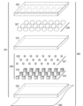
図3A、図3B及び図3Cは、本開示の種々の実施形態による位相を合わせた画像層を有するマイクロ光学セキュリティデバイス及びセキュリティ文書の例を示している。便宜上、図3C~図3Cのうちの1つ以上に共通の構造には同じ番号が付されている。 Figures 3A, 3B, and 3C illustrate examples of micro-optical security devices and security documents having image layers in phase according to various embodiments of the present disclosure. For convenience, structures common to one or more of FIGS. 3C-3C are numbered the same.
図3Aの非限定的な例を参照すると、本開示の種々の実施形態によるマイクロ光学セキュリティデバイス301の一例が図に示されている。
Referring to the non-limiting example of FIG. 3A, one example of a
図3Aの非限定的な例を参照すると、マイクロ光学セキュリティデバイス301は、基本的なレベルにおいて、(例えば集光素子307を含む)集光素子の平面アレイ305と、(例えば画像アイコン321を含む)第1のアイコン層320及び(例えば画像アイコン324を含む)第2の画像アイコン層323を備えたアイコン層スタック308とを含む。種々の実施形態によると、集光素子の平面アレイ305の各集光素子はフットプリントを有する。さらに、集光素子の平面アレイは1つ以上のセルを含み、このセルには、第1のアイコン層320又は第2の画像アイコン層323の配列の1つ以上の画像アイコンが配置されている。さらに、アイコン層スタック308は、第1のアイコン層320の着色画像アイコン及び第2の画像アイコン層323の着色画像アイコンが位相合わせされた少なくとも1つの領域を含む。特定の実施形態では、画像アイコン(例えば画像アイコン321又は324)の位置は、UV硬化性樹脂などのほぼ透明な材料からなる保持構造内の位置に対応しており、このほぼ透明な材料をエンボス加工し、次に硬化させて、着色材料を選択的に堆積させることのできるボイド、ポスト又はメサなどの構造を有する画像アイコン層を形成する。いくつかの実施形態によると、集光素子の平面アレイ305の個々の集光素子は1つ以上の局所反復周期で配置される。本開示で使用される「局所反復周期」という用語は、マイクロ光学セキュリティデバイス301の層の特定の特徴が対象領域内でどれだけ頻繁に反復するかに関する表現を包含している。一例として、集光素子の平面アレイ305の集光素子は、システムの1つの領域において1mm当たり50レンズ、異なる部分において1mm当たり49レンズの局所反復周期を有することができる。同様に、第1のアイコン層320内の着色アイコンは、例えば、マイクロ光学セキュリティデバイス301の1つの部分において1mm当たり51アイコンの局所反復周期と、マイクロ光学セキュリティデバイス301の異なる領域において1mm当たり49.5アイコンの局所反復周期とを有することができる。集光素子の局所反復周期とアイコン構造の比を変えることにより、集光素子によって投影されるアイコン構造の合成画像の外観を調整することができる。例えば、マイクロ光学セキュリティデバイス301の平面に対する合成画像の見かけの位置を、集光素子の局所反復周期とアイコン構造の局所反復周期の比によって変更し、合成画像がマイクロ光学セキュリティデバイス301の平面の上に浮いて見えるように、又はマイクロ光学セキュリティデバイス301の平面の下に位置して見えるように(「ディープ」又は「スーパーディープ」効果と呼ばれることもある)することができる。同様に、特定の実施形態では、集光素子の局所反復周期と着色アイコン構造の局所反復周期の比自体を局所的に変更し、より3次元的な外観を合成画像に付与することができる。
Referring to the non-limiting example of FIG. 3A, a
特定の実施形態によると、複数の集光素子305はマイクロ光学集光素子の平面アレイを含む。いくつかの実施形態において、集光素子の平面アレイ305の集光素子は、屈折率の異なる領域(例えばポリマーレンズ材料と空気)の間に湾曲した界面を提供するレンズ表面を有するマイクロ光学屈折集光素子(例えば平凸レンズ又はGRINマイクロレンズ)を含む。集光素子の平面アレイ305の屈折集光素子は、いくつかの実施形態では1.35~2.05の範囲の屈折率を有する光硬化樹脂から製造され、5μm~200μmの範囲の直径を有する。種々の実施形態において、集光素子の平面アレイ305の集光素子は、直径が5μm~50μmに及ぶ反射集光素子(例えば、非常に小さな凹面ミラー)を含む。この説明のための例では、集光素子の平面アレイ305の集光素子は円形の平凸レンズを含むものとして示されているが、他の屈折レンズ形状、例えばレンチキュラーレンズが可能であり、本開示の想定範囲内にある。
According to certain embodiments, the plurality of
図3Aの説明のための例に示すように、第1の画像アイコン層320は、指向性硬化(directional curing)角度の範囲に関連する集光素子の平面アレイ305の集光素子のフットプリント内の位置に配置された(画像アイコン321を含む)画像アイコンのセットを含む。種々の実施形態によると、第1のアイコン層320の個々の画像アイコンは、ほぼ透明な材料から形成される構造化された画像アイコン層の保持構造によって画定される部分的又は全てのスペースに指向性硬化(directionally cured)材料の領域を含む。本開示で使用されるように、「構造化された画像層」という用語は、画像アイコン材料を配置して保持するための構造(例えば、凹部、ポスト、溝又はメサ)を含むようにエンボス加工されたか又は他の方法で形成されたほぼ透明な材料(例えば光硬化性樹脂)の層を包含する。
As shown in the illustrative example of FIG. 3A, the first
図3Aの説明のための例に示すように、特定の実施形態において、マイクロ光学システム301は光学スペーサ310を含む。種々の実施態様によると、光学スペーサ310は、集光素子の平面アレイ305の集光素子の焦点面内又はその周囲に、アイコン層スタック308の画像アイコンの1つ以上の配列の画像アイコンを配置するよう機能するほぼ透明な材料のフィルムを含む。本開示による特定の実施形態において、光学スペーサ310は製造基板を含み、これに光硬化性材料の1つ以上の層を塗布し、エンボス加工し、フラッド硬化させて保持構造を形成することができる。特定の実施形態において、第1のアイコン層320を形成するために使用される光硬化性材料は紫外線(UV)硬化性の着色ポリマーである。本開示による種々の実施形態において、光学スペーサ310は、集光素子とアイコン層スタック308との間にある、透明なUV硬化性ポリマー(例えば、集光素子の平面アレイ305の集光素子を作製するために使用されるポリマー)の塗布された中間層を含む。
In certain embodiments, the
本開示による特定の実施形態において、マイクロ光学セキュリティデバイス301はシール層340を備えている。特定の実施形態によると、シール層340は、下面において集光素子の平面アレイ305の集光素子とつながるほぼ透明な材料の薄い(例えば2μm~50μmの厚さの)層を含み、(例えば、滑らかであるか、局所的な起伏の曲率半径が集光素子よりも大きな表面を有することによって)集光素子の平面アレイ305よりも曲率のばらつきが少ない上面を含む。
In certain embodiments according to the present disclosure,
図3Aの非限定的な例に示すように、特定の実施形態において、マイクロ光学セキュリティデバイス301を例えば接着層330によって基板350に取り付け、セキュリティ文書360(例えば、図1A~図1Bのセキュリティ文書105)を形成することができる。種々の実施形態によると、基板350を紙幣のシート又はポリマー基板とすることができる。いくつかの実施形態によると、基板350は、ポリマーフィルムである二軸延伸ポリプロピレン(BOPP)の薄い可撓性シートである。種々の実施形態において、基板350はテスリン(登録商標)などの合成紙材の一部である。いくつかの実施形態によると、基板350は、クレジットカード及び運転免許証の作成に適したタイプのポリエチレンテレフタレート(PET)ブランクのようなポリマーカード材料の一部である。特定の実施形態において、基板350は、ボトルなどの製品、セキュリティ文書、又はスマートフォンやコンピュータのような価値の高い商品の表面を含む。
As shown in the non-limiting example of FIG. 3A, in certain embodiments,
図3Aは、第1のアイコン層320及び第2の画像アイコン層323の双方がほぼ透明な材料から構築された構造化画像アイコン層内に形成されたマイクロ光学セキュリティデバイス301の例を示しているが、本開示による実施形態はこれに限定されない。保持構造を作製するために光硬化性材料の薄い層をエンボス加工するツールを作製する技術は成熟しており、マイクロ光学セキュリティデバイスを大量生産するツールと一体化されているが、画像アイコンを作製する他の技術も可能であり、本開示の種々の実施形態による位相合わせされたアイコン層を有するマイクロ光学セキュリティデバイスの構造化アイコン層に関連して使用することができる。例えば、本開示による特定の実施形態では、デジタルツーリング方法を用いて画像アイコンの配列又は画像アイコンの第2の配列のいずれかを作製することができる。本開示で使用されるデジタルツーリングは、マイクロ光学セキュリティデバイスの構成構造(例えば画像アイコン又は集光素子)を、構成構造の形成及び配置に用いる電子ツールの制御論理(例えばプリンタ用のGコードファイル)を定義することによって製造する方法を包含する。本開示の図5及び図8の説明のための例を参照してより詳細に述べられるように、特定の実施形態によると、画像アイコンの第1又は第2の配列のいずれかの画像アイコンは、デジタルツーリングを用いて表面実装アイコンとして作製が可能である。
FIG. 3A shows an example of a
本開示の種々の実施形態によるデジタルツーリングのさらなる例として、1つ以上のデジタル制御されたUVプロジェクタは、紫外線のパターン(例えば、マイクロ光学セキュリティデバイスによって投影される合成画像の全部又は一部に対応するマスクファイル)を未硬化の透明な又は着色した光硬化材料の層上に投影して表面実装画像アイコンを作製することができる。特定の実施形態において、1つ以上のUVプロジェクタは集光素子の層を通してパターン紫外線を投影し、これによって未硬化の光硬化性材料の部分を指向性硬化させる。種々の実施形態では、デジタル制御されたUVプロジェクタの代わりに、ラスタ化されたUVレーザビームによってUV光のパターンを未硬化の材料上に投影することができる。 As a further example of digital tooling according to various embodiments of the present disclosure, one or more digitally controlled UV projectors correspond to a pattern of ultraviolet light (e.g., all or part of a composite image projected by a micro-optical security device). A mask file) can be projected onto a layer of uncured clear or colored light curable material to create a surface mount image icon. In certain embodiments, one or more UV projectors project patterned UV light through the layer of concentrating elements, thereby directionally curing portions of the uncured photocurable material. In various embodiments, instead of a digitally controlled UV projector, a rasterized UV laser beam can project the pattern of UV light onto the uncured material.
図3Bの非限定的な例を参照すると、この特定の例では、第1の画像アイコン層320は図3Aと同一の構造を有し、ここで画像アイコンは保持構造によって画定されるスペース内に配置された着色材料の領域として形成されており、保持構造は、この特定の例ではエンボス加工を施して硬化させたポリマー層の層を含む。特定の実施形態によると、第1のアイコン層320内の保持構造を第1の色の光硬化性液体材料で充填し、次に指向性硬化させ、これによって光硬化性材料の一部が固体状態に硬化されるのに対し、光硬化性材料の別の部分は液体状態のままであり、洗浄などによって保持構造から除去することができる。
Referring to the non-limiting example of Figure 3B, in this particular example, the first
本開示で使用される「指向性硬化」という用語は、集光素子によって、視野角に関連する画像アイコン層内の位置を占める未硬化材料上に光が集束されるように、マイクロ光学セキュリティデバイスによって提供される合成画像に基づいたパターンの構造化光又は半構造化光(例えばコリメート光)を、合成画像の意図された視野角範囲に関連する位置に配置された光源(又は複数の光源)から、集光素子のアレイの素子に向かって投影することを包含する。換言すれば、例えば本開示の図6A~図6Iの説明的な例を通して説明されるように、視野角範囲に関連する光源からの光であり、集光素子のアレイ(例えば、図3Aの集光素子の平面アレイ305)の集光素子によって集束された光の焦点経路に沿った未硬化材料は硬化されるのに対し、集光素子によって集束された指向性硬化光の焦点経路の外側の位置にある未硬化材料は未硬化のままである。 The term "directional curing" as used in this disclosure refers to a micro-optical security device such that light is focused by a light collection element onto an uncured material occupying a position within the image icon layer that is related to the viewing angle. A pattern of structured or semi-structured light (e.g., collimated light) based on a composite image provided by a light source (or light sources) positioned at positions associated with the intended viewing angle range of the composite image. from toward an element of an array of light collecting elements. In other words, the light from the light source associated with the viewing angle range, such as illustrated through the illustrative examples of FIGS. Uncured material along the focal path of the light focused by the light collecting elements of the planar array of light elements 305) is cured, whereas the directional curing material outside the focal path of the light focused by the light collecting elements is cured. Uncured material at the location remains uncured.
特定の実施形態によると、第1の色の未硬化材料を保持構造から洗浄した後、他の色の指向性硬化材料、又は異なる視野角に関連する指向性硬化材料のさらなる反復が行われる。図3Bの説明のための例では、第1のアイコン層320の形成における最終ステップは、オープンなスペース(例えば、硬化した着色材料によって占有されていない領域)を、少なくとも人間の目には殆ど又は全く見えないほぼ透明な光硬化性材料で充填することである。特定の実施形態によると、電子顕微鏡などの画像化機器を用いてほぼ透明な材料の層を検出することができる。
According to certain embodiments, after the uncured material of the first color is washed from the holding structure, further iterations of directionally cured material of other colors or associated with different viewing angles are performed. In the illustrative example of FIG. 3B, the final step in forming the
図3Bの非限定的な例を参照すると、特定の実施形態によれば、アイコン(例えば表面実装アイコン326)、すなわち第2のアイコン層328の硬化着色材料の容積を、本明細書に記載する少なくとも2つの方法によって第1のアイコン層320の表面に形成することができる。
Referring to the non-limiting example of FIG. 3B, according to certain embodiments, the icon (eg, surface mount icon 326), i.e., the volume of hardened colored material of the
特定の実施形態によると、第1のアイコン層320の表面に表面実装アイコンを作製する1つの方法では、光硬化性ポリマーの層をエンボス加工し、次にフラッド硬化させるなど、まず保持構造のセットを作製することによって第1のアイコン層320を形成する。種々の実施形態では、第2のステップにおいて、未硬化のほぼ透明な光硬化性材料で保持構造をさらに充填し、その余剰分を保持構造からドクターブレードで除去し(doctor bladed off)、第1の視野角範囲に関連する指向性硬化光のパターンを用いて保持構造内の材料を指向性硬化させ、第1の視野角範囲に関連する硬化したほぼ透明な材料からなる第1のアイコン層320内に領域を作成する。続いて、未硬化のほぼ透明な光硬化性材料を保持構造から洗浄し、依然として利用可能な保持構造を第1の色の未硬化の光硬化性材料で充填又はコーティングし、その余剰分を保持構造からドクターブレードで除去し、残りの材料をフラッド硬化させ、集光素子の平面アレイ305に対して遠位のほぼ平坦な外面を有する第1のアイコン層320を完成させる。特定の実施形態によると、第1のアイコン層320を形成する第2のステップと同様に、第2の色の未硬化光材料を外面に塗布し、第1の視野角範囲に関連する光を用いて指向性硬化させる。指向性硬化に続き、第2の色の未硬化の光硬化性材料を外面から洗浄し、第2のアイコン層328の表面実装アイコンが第1のアイコン層の外面に残る。
According to certain embodiments, one method of making surface mount icons on the surface of the
特定の実施形態によると、表面実装画像アイコンの第2のアイコン層328を形成する別の方法は、前述のように第1のアイコン層320を作製するステップと、第2の色の未硬化の光硬化性材料の層を塗布するステップとを含む。第2の色の未硬化の光硬化性材料は、第1の色の材料を硬化させた第1の角度範囲に対して相補的な角度で、パターン化された光を用いて指向性硬化させる。このようにして、第1の色の着色材料の合成画像が集光素子を通して投影される角度範囲と、第2の色の着色材料の合成画像が集光素子を通して投影される角度範囲との間の分離を制御することができる。
According to a particular embodiment, another method of forming the
図3Cは、本開示の種々の実施形態によるマイクロ光学セキュリティデバイス301の例を示している。
FIG. 3C illustrates an example
表面実装アイコンを含む画像アイコン層が、複数のほぼ透明な保持構造を含む別の画像アイコンに対して集光素子のアレイの遠位にある、本開示によるマイクロ光学セキュリティデバイスの例を示した図3Bの説明のための例に加え、図3Cは、表面実装した画像アイコンの層がほぼ透明な保持構造を含むアイコン層に対して集光素子の近位にあるマイクロ光学セキュリティデバイス301の例を示している。
FIG. 10 illustrates an example of a micro-optical security device according to the present disclosure in which an image icon layer containing surface mounted icons is distal to an array of light collection elements relative to another image icon containing a plurality of substantially transparent holding structures; In addition to the illustrative example of 3B, FIG. 3C shows an example of a
図3Cの非限定的な例を参照すると、第1のアイコン層327は、第1の視野角範囲にわたって光を提供するように配置された構造化光源からの、第1の合成画像に関連する光のパターンを用いて第1の色の未硬化着色材料の層を指向性硬化させることにより光学スペーサ310側に形成された、(表面実装画像アイコン329を含む)複数の表面実装画像アイコンを含む。この説明のための例では、指向性硬化に続いて第1の色の未硬化材料を除去し、任意選択により、異なる色又は異なる視野角に関連する表面実装アイコンの後続のセットを、第1の色又は他の色の指向性硬化材料によって形成する。未硬化の着色材料を光学スペーサ310の表面から除去し、ほぼ透明な材料の層を塗布して表面実装画像アイコン間のスペースを充填し、平坦な表面を形成して、その上に第2の画像アイコン層323を、保持構造を含む画像アイコン層として形成することができる。種々の実施形態によると、ほぼ透明な材料の層は、第1のアイコン層327のほぼ透明な材料が第2の画像アイコン層323の保持構造と一体化されるように塗布される。
Referring to the non-limiting example of FIG. 3C, a
いくつかの実施形態では、第2の画像アイコン層323の保持構造を第2の色の未硬化の光硬化性材料で充填し、次に、これをドクターブレードにかけて余剰の未硬化材料を除去する。第2の色の未硬化の光硬化性材料を、第1の視野角範囲に関連する光のパターンで指向性硬化させ、第2の色の未硬化材料を洗い流す。アイコン層スタック308に指定された層の数に応じて、いくつかの実施形態では、アイコン層スタック308を製造するプロセスは、さらなる充填/硬化工程を行わずにここで終了することができる。
In some embodiments, the retaining structures of the second
図4A及び図4Bは、本開示の種々の実施形態によるマイクロ光学セキュリティデバイス(例えば、図1A~図1Bのマイクロ光学セキュリティデバイス110)の積み重ねられたアイコン層の寄与の態様を示している。本開示の種々の実施形態によるマイクロ光学セキュリティデバイスはアイコン層スタックを含む。アイコン層スタックは集光素子のアレイによって拡大されて合成画像を投影し、この合成画像は、多色合成画像を含むがこれに限定されず、マイクロ光学セキュリティデバイスによって提供される合成画像にアイコン層スタックの各層が寄与する視野角範囲が厳密に制御された、特徴的で注意を引く光学効果をもたらす。本明細書の他の箇所で述べられるように、本開示のいくつかの実施形態によるマイクロ光学セキュリティデバイスは、位相合わせされた画像アイコン層を有するアイコンスタックを含む。
FIGS. 4A and 4B illustrate aspects of stacked icon layer contributions of micro-optical security devices (eg,
図4A~図4Bの説明のための例を参照すると、第1の視野角範囲(Θ1→Θ2)及び第2の視野角範囲(Θ2→Θ3)にわたってシステムによって投影される合成画像に対する第1の画像アイコン層(例えば、図3Aの第1のアイコン層320)及び第2の画像アイコン層(例えば、図3Bの第2のアイコン層328)の寄与が図示されている。相互参照の便宜上、図4の例においてマイクロ光学セキュリティデバイスによって観察者に投影される合成画像は、図1A~図1Bの説明のための例に示される合成画像に対応する。すなわち、第1の視野角範囲内の角度で見た場合、マイクロ光学デバイスは、第1の色の楕円の対を第2の色の背景上に投影する。この非限定的な例では、第1の色の画像アイコンを含む第1の画像アイコン層のアイコンと、第2の色の画像アイコンを含む第2の画像アイコン層のアイコンとの間の位相合わせのおかげで、視野角が第1の視野角範囲から第2の視野角範囲に遷移し、着色された楕円は「オフに切り替わり」、第2の色の合成画像に置き換えられる。
Referring to the illustrative example of FIGS. 4A-4B, a composite image projected by the system over a first viewing angle range (Θ 1 →Θ 2 ) and a second viewing angle range (Θ 2 →Θ 3 ). The contribution of a first image icon layer (eg,
図4A~図4Bに示すように、マイクロ光学セキュリティデバイスを第1の視野角範囲(Θ1→Θ2)で見た場合、第1のアイコン層が合成画像で見える領域を第1の楕円401a及び第2の楕円401bとして寄与するように、デバイスの集光素子は第1の色の硬化材料の指向性容積を含む第1のアイコン層の領域を投影する。いくつかの実施形態によると、第1のアイコン層の第1の色の未硬化材料を楕円401a及び401bに関連するパターンで指向性硬化させるとともに、第2のアイコン層の未硬化のほぼ透明な材料も楕円401a及び401bに関連するパターンで指向性硬化させ、第1の視野角範囲に関連する焦点経路から第2の色の着色材料を除外し、第2のアイコン層の対応する領域403a及び403bが、楕円401a及び401bを生じる第1のアイコン層の領域とクロストークしないか又は他の方法で干渉しないことを確実にする。
As shown in FIGS. 4A-4B, when the micro-optical security device is viewed in a first viewing angle range (Θ 1 →Θ 2 ), a
同様に、第2の視野角範囲(Θ2→Θ3)について、特定の実施形態では、未硬化のほぼ透明な材料を第1の層に塗布し、第2の視野角範囲に関連する光源から指向性硬化させ、これにより、第2の視野角範囲においてマイクロ光学セキュリティデバイスによって投影される合成画像に対する第1のアイコン層の寄与405がないことを確実にする。すなわち、いくつかの実施形態では、第1のアイコン層で、第2の視野角範囲に関連する角度に沿ってマイクロ光学セキュリティデバイスに出入りする光の焦点経路に関連する位置には着色材料がない。
Similarly, for the second viewing angle range (Θ 2 →Θ 3 ), in certain embodiments, an uncured substantially transparent material is applied to the first layer and the light source associated with the second viewing angle range is to ensure that there is no
さらに、第2の視野角範囲(Θ2→Θ3)について、本発明による種々の実施形態では、第2の色の未硬化材料の容積を、第2の視野角範囲に関連する光源からもたらされる構造化光で指向性硬化させる。よって、第2の視野角範囲では、第2の画像アイコン層は、第2の画像アイコン層のみから描画された成分を有する合成画像407を投影する。
Further, for a second viewing angle range (Θ 2 →Θ 3 ), various embodiments in accordance with this invention provide a volume of uncured material of a second color from a light source associated with the second viewing angle range. directionally cured with structured light. Thus, in the second viewing angle range, the second image icon layer projects a
アイコン層スタックの層における第1の色の着色材料を指向性硬化させ、第2のアイコン層の未着色材料を同じ視野角範囲において指向性硬化させることによって生じる単一の「フリッカ」効果を提供するマイクロ光学セキュリティデバイスを参照して図4A~図4Bを説明したが、本開示による実施形態はこれに限定されない。例えば、特定の実施形態では、アイコン層の位相整合と、画像アイコンスタックの各層の着色材料が合成に寄与する視野角とを制御する技術を適用して種々の効果を生じることができる。例えば、特定の実施形態では、合成画像の一部分は、図4を参照して説明したような、視野角が第1の視野角範囲外に移動した直後に1つの色が「遮断」される位相合わせを示し、合成画像の異なる部分は、色が視野角と共に変化するわずかな位相ずれを示すことができる。さらに、特定の実施形態では、図3Bを参照して説明したように、第1の画像アイコン層の着色材料を指向性硬化させるために使用される第1の視野角範囲と相補的な視野角範囲において第2の画像アイコン層の未硬化材料を指向性硬化させることにより、第1の画像アイコン層の着色材料と第2の画像アイコン層の着色材料との間の位相合わせを実現することができる。 Providing a single "flicker" effect caused by directionally curing a first color pigmented material in a layer of an icon layer stack and directionally curing an unpigmented material of a second icon layer in the same viewing angle range. Although FIGS. 4A-4B have been described with reference to a micro-optical security device, embodiments in accordance with the present disclosure are not so limited. For example, in certain embodiments, techniques for controlling the phasing of icon layers and the viewing angle at which the colorant material of each layer of the image icon stack contributes to the composition can be applied to produce various effects. For example, in certain embodiments, a portion of the composite image is phased such that one color is "blocked" immediately after the viewing angle moves out of the first viewing angle range, such as described with reference to FIG. Showing alignment, different parts of the composite image can exhibit a slight phase shift where color changes with viewing angle. Further, in certain embodiments, viewing angles complementary to the first viewing angle range used to directionally cure the colorant material of the first image icon layer, as described with reference to FIG. 3B Directional curing of the uncured material of the second image icon layer in an area can achieve phasing between the color material of the first image icon layer and the color material of the second image icon layer. can.
図5A~図5Cは、本開示の特定の実施形態によるマイクロ光学セキュリティデバイスのセルに表面実装画像アイコンを形成する態様を複数の視点から示している。 5A-5C illustrate aspects of forming surface mounted image icons on cells of a micro-optic security device from multiple perspectives according to certain embodiments of the present disclosure.
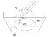
本開示による特定の実施形態において表面実装画像アイコンを形成するために、構造化光が、所定の視野角範囲に対応する投影角度から集光素子の平面アレイの集光素子のレンズ面に投影され、構造化光は、集光素子の平面アレイの集光素子によって、集光素子の平面アレイの集光素子のフットプリント内にある未硬化の光硬化性材料の領域上に集束される。続いて、光硬化性材料の硬化領域のみが所定の視野角範囲において集光素子を通して可視になるように、未硬化の光硬化性材料を(例えばスプレー洗浄を用いて)除去するか、又は化学的に不活性化させる。このようにして、着色材料(例えば画像アイコン)又はほぼ透明な材料(例えば、アイコン層スタックの別の層における着色アイコンの寄与を妨げる位置から着色材料を排除するため)の硬化した容積をマイクロ光学セキュリティデバイスの表面に形成することができる。 To form a surface mount image icon in certain embodiments according to the present disclosure, structured light is projected onto the lens surfaces of the light collecting elements of the planar array of light collecting elements from a projection angle corresponding to a predetermined viewing angle range. , the structured light is focused by the light collecting elements of the planar array of light collecting elements onto areas of uncured photocurable material within the footprint of the light collecting elements of the planar array of light collecting elements. Uncured photocurable material is then removed (e.g., using spray cleaning) or chemically removed so that only the cured regions of the photocurable material are visible through the light collection element in the predetermined viewing angle range. effectively inactivate. In this way, a cured volume of colored material (e.g., image icons) or substantially transparent material (e.g., to exclude colored material from locations that interfere with the contribution of colored icons in another layer of the icon layer stack) is micro-optically It can be formed on the surface of the security device.
図5A~図5Cの非限定的な例を参照すると、光学スペーサ503の一部に配置された屈折集光素子501の側面図(図5C)、底面図(図5A)及び斜視図(図5B)が提供されている。この説明のための例において、集光素子501のレンズ面510は、異なる屈折率の領域間の湾曲した境界(例えば、1よりも大きい屈折率を有するポリマーと空気)を画定し、この湾曲した境界は硬化光をレンズのフットプリント内の位置に導き、そこで硬化光は第1の色の光硬化性材料の容積を硬化させ、表面実装画像アイコン521を形成する。
Referring to the non-limiting examples of FIGS. 5A-5C, a side view (FIG. 5C), bottom view (FIG. 5A) and perspective view (FIG. 5B) of a refractive focusing
特定の実施形態によると、集光素子501は光スペーサ503に固着され、光学スペーサ503の表面に対して固定された関係を有する。特定の実施形態では、集光素子501と光学スペーサ503の表面との固定された関係は、光硬化性材料の層を光学スペーサ503に塗布し、光硬化性材料の層をエンボス加工してレンズ表面を形成し、材料をその場で硬化させることによって実現される。いくつかの実施形態では、集光素子501と光スペーサ503の表面との固定された関係は、集光素子501と光スペーサとの双方を光硬化性材料からなる共通の層から形成し、形成した層を硬化させて一体化した集光素子-光学スペーサの組み合わせを作製することによって実現される。
According to certain embodiments,
集光素子501は、集光素子501によって画像アイコンを投影できる十分な鮮鋭度で集光素子501が光を集束することのできる領域を画定するフットプリント505に関連付けられている。図5A~図5Cの例に示されるように、フットプリント505を3次元のスペース領域とすることができ、これにより、アイコン層スタックの複数層のアイコンはフットプリント505内のスペースを占有することができる。いくつかの実施形態によると、フットプリント505は集光素子501の周縁と同じ広がりをもつ。いくつかの実施態様によると、フットプリント505は集光素子501の周縁よりも小さい。特定の実施形態では、フットプリント505は集光素子501の周縁よりも大きい領域を示している。
図5A~図5Cの説明のための例に示すように、図5A~図5Cに示すセルなどの合成画像に関連する構造化光(例えば、コリメート光、プロジェクターからの光、又は集光素子の他のアレイを通過した光)は、この図にΘcとして示す所定の視野角に関連する角度(又は角度範囲)で集光素子501のレンズ表面に投影される。集光素子501のレンズ作用により、入射光がフットプリント505内の焦点経路520に沿って集束される。構造化光をシステムに用いる前に未硬化の光硬化性着色(又はほぼ透明な光硬化性)材料の層を光学スペーサ503の底面に塗布することにより、構造化光を続けて用いることで焦点経路520にある光硬化性材料の部分が硬化するのに対し、焦点経路520外の光硬化性材料の部分は未硬化のままであり、これを除去することができる。したがって、表面実装画像アイコン521を集光素子501のフットプリント505内の表面に形成することができる。
As shown in the illustrative example of FIGS. 5A-5C, structured light (eg, collimated light, light from a projector, or light collection element associated with a composite image such as the cells shown in FIGS. 5A-5C). light passing through the other arrays) is projected onto the lens surface of
図6A~図6Iは、本開示の種々の実施形態によるマイクロ光学セキュリティデバイスの構造の態様を示している。相互参照の便宜上、図6A~図6Iのうち2つ以上に共通する要素には同様の番号を付している。 6A-6I illustrate aspects of the construction of micro-optical security devices according to various embodiments of the present disclosure. For ease of cross-reference, elements common to two or more of FIGS. 6A-6I are similarly numbered.
図6Aの非限定的な例を参照すると、本開示の特定の実施形態によるマイクロ光学セキュリティデバイスの集光素子の平面アレイ601のセクションが図に示されている。図に示すようないくつかの実施形態において、集光素子の平面アレイ601の集光素子は平凸マイクロレンズである。いくつかの実施形態では、集光素子の平面アレイ601の集光素子は反射集光素子又は異なる屈折構造体(例えばGRINレンズ)である。図に示すように、集光素子の平面アレイ601のセクションの集光素子は局所反復周期P1を有し、これは、図に示す集光素子の平面アレイ601のセクションにおいて同様のサイズの集光素子のパターンが繰り返される間隔(distance)に対応する。
Referring to the non-limiting example of FIG. 6A, a section of a
特定の実施形態において、角度Θa、又はΘaを含む視野角範囲において集光素子の平面アレイ601上に投影された光は集光素子603の平面アレイの構成素子によって集束され、複数の焦点経路610(例えば焦点経路611を含む)に沿って、マイクロ光学セキュリティデバイスの光学スペーサ605及び後続の層(例えばアイコン層スタック)を通過する。
In certain embodiments, light projected onto the planar array of concentrating
特定の実施形態によると、マイクロ光学セキュリティデバイスは、ポリエチレン又はポリエステルフィルムなどほぼ透明な材料のシートを備えた光学スペーサ605を含み、この上に集光素子及びアイコン層スタック(例えば図3Aのアイコン層スタック308)を形成することができる。いくつかの実施形態によると、光学スペーサ605は、集光素子の平面アレイ601など、マイクロ光学セキュリティデバイスの他の構造を作製するために使用されるほぼ透明な光硬化性ポリマーの中間層を含む。本開示による種々の実施形態では、光学スペーサ605は二軸延伸ポリプロピレン(BOPP)、ポリカーボネート、ポリ塩化ビニル(PVC)又はポリエチレンテレフタレート(PET)フィルムのセクションを含む。
According to a particular embodiment, the micro-optical security device includes an
図6Bは、本開示の特定の実施形態によるマイクロ光学セキュリティデバイスの構成の態様を示している。図6Bの説明のための例を参照すると、アイコン層スタック(例えば図3Aのアイコン層スタック308)の第1のアイコン層の作製における最初のステップが図に示されている。特定の実施形態によると、複数の保持構造607が光学スペーサ605の下側に形成される。この説明の例では、複数の保持構造607は、ほぼ透明な材料の層に形成された1組の起伏(reliefs)又は凹部(図では点の塗りつぶしで示されている)を含む。図に示すように、複数の保持構造607は、図6Bに示すマイクロ光学セキュリティデバイスのセクションにおいて局所反復周期P2を有する。本発明による特定の実施形態では、第1のアイコン層によって投影される合成画像の成分がマイクロ光学セキュリティデバイスの物理面に対して異なる高さで現れるように、アイコン層スタックの第1のアイコン層の保持構造の局所反復周期P2はアイコン層にわたって変化する。
FIG. 6B illustrates aspects of the configuration of a micro-optical security device according to certain embodiments of the present disclosure. Referring to the illustrative example of FIG. 6B, the initial steps in creating the first icon layer of an icon layer stack (eg,
いくつかの実施形態によると、複数の保持構造607は、第1の色の未硬化の光硬化性材料609で充填されている。
According to some embodiments, the plurality of retaining
図6Cは、本開示の特定の実施形態によるマイクロ光学セキュリティデバイスの構造の態様を示している。 FIG. 6C illustrates aspects of the construction of a micro-optical security device according to certain embodiments of the present disclosure.
図6Cの非限定的な例を参照すると、画像アイコンスタックの第1の画像アイコン層によって投影させる合成画像の成分に関連する構造化光が集光素子の平面アレイ601において投影され、光学スペーサ605、複数の保持構造607、及び第1の色の未硬化の光硬化材料609の容積を通過する。この非限定的な例に示すように、光学スペーサ605を通過する光の焦点経路は、第1の色の未硬化光材料の容積の全てを包含するわけではない。例えば、第1の保持構造608内の第1の色の光硬化性材料609のうち、第1の部分613aは焦点経路611の外側にあるのに対し、第2の部分613bは焦点経路611内にある。いくつかの実施形態によると、第1の部分613aは焦点経路611に沿って通過する硬化光によって硬化されないのに対し、焦点経路611内にある第2の部分613bは焦点経路611に沿って通過する光によって硬化される。同様に、第1の色の光硬化性材料の第3の容積613cは焦点経路611及び隣接する焦点経路の完全に外側にあり、未硬化のままである。
Referring to the non-limiting example of FIG. 6C, structured light associated with components of a composite image to be projected by the first image icon layer of the image icon stack is projected at
図6Dは、本開示の種々の実施形態によるマイクロ光学セキュリティデバイスの構造の態様を示している。 FIG. 6D illustrates aspects of the structure of a micro-optical security device according to various embodiments of the present disclosure.
この説明のための例に示されるように、第1の視野角範囲からの構造化光(例えば、図6Cの複数の焦点経路610に沿って進む光)で第1の色の光硬化性材料を指向性硬化させた後、未硬化材料が複数の保持構造607から除去され、焦点経路611内にあった複数の保持構造613のスペースにある第1の色の硬化材料の容積のみが残る。例えば、部分613a及び613cの未硬化材料の容積が指向性硬化後に除去されたのに対し、第2の部分613bは複数の保持構造607内の所定の位置に残っている。
As shown in this illustrative example, structured light from a first viewing angle range (e.g., light traveling along multiple
図6Eは、本開示のいくつかの実施形態によるマイクロ光学セキュリティデバイスの構造の態様を示している。図6Eの説明のための例を参照すると、硬化材料の容積(例えば第2の部分613b)を特定の焦点経路(例えば図6Cの焦点経路611)に関連する複数の保持構造607内の位置に「閉じ込める」のを助けるために、保持構造607の残りの未充填領域をほぼ透明な材料(例えば、集光素子の平面アレイ601を形成するためにエンボス加工及び硬化に適したUV硬化性ポリマー)で充填する。特定の実施形態によると、指向性硬化材料によって充填されていないスペースを充填するために保持構造に追加されたほぼ透明な材料は、ほぼ透明な保持構造と追加のほぼ透明な材料との間に界面領域(例えば界面領域615)を生じる。ほぼ透明な材料からなるこれらの領域間の境界を含む界面領域は、人間の目には見えないが電子顕微鏡で見ることができる。
FIG. 6E illustrates aspects of the structure of a micro-optical security device according to some embodiments of the present disclosure. Referring to the illustrative example of FIG. 6E, a volume of curable material (eg,
本開示による特定の実施形態では、複数の保持構造607の未充填領域にほぼ透明な材料を追加することによって第1のアイコン層620の構築が完了し、この上にアイコン層スタックの第2又はそれより上のアイコン層を形成することができる。
In certain embodiments according to the present disclosure, the construction of the
図6Fは、本開示の種々の実施形態によるマイクロ光学セキュリティデバイスの構造の態様を示している。 FIG. 6F illustrates aspects of the construction of micro-optical security devices according to various embodiments of the present disclosure.
特定の実施形態によると、多層(すなわち、2つ以上の層)からなるアイコン層スタックの第2の層が、集光素子の平面アレイ601に対して遠位側の第1のアイコン層620の表面に形成される。図6Fの非限定的な例に示されるように、第2の複数の保持構造631が、(例えば、ほぼ透明なUV硬化性材料の層をエンボス加工し、続いて硬化させることにより)集光素子の平面アレイ601に対して遠位側の第1のアイコン層620の表面に形成される。
According to certain embodiments, the second layer of the icon layer stack of multiple layers (i.e., two or more layers) is the
図6Fの非限定的な例を参照すると、第2の複数の保持構造631の凹部は、未硬化のほぼ透明な光硬化性材料633の容積で充填されている。次に、第1のアイコン層620の第1の色の光硬化性材料を硬化させるために用いる光と同様に、複数の焦点経路610に沿ってアイコン層スタックの構造を通過して移動する光により、未硬化のほぼ透明な光硬化性材料633を指向性硬化させる。図6Fの例に示すように、未硬化のほぼ透明な光硬化性材料の容積は、第2の複数の保持構造631内の、複数の焦点経路610の焦点経路と一致する位置において硬化される。例えば、第1の容積635aを占める光硬化性材料は焦点経路611に沿って進む光によって硬化されるのに対し、焦点経路611の外側にある位置635bを占める光硬化性材料は未硬化のままである。
Referring to the non-limiting example of FIG. 6F, the recesses of the second plurality of retaining
図6Gは、本開示の特定の実施形態によるマイクロ光学セキュリティデバイスの構造の態様を示している。特定の実施形態によると、第2の複数の保持構造631内の未硬化のほぼ透明な光硬化性材料633が除去される。ほぼ透明な光硬化性材料は第1の視野角範囲に関連する位置(例えば複数の焦点経路610上の位置)で硬化されるため、第1の複数の焦点経路に沿ってアイコン層スタックを通過する光の焦点経路の外側の視野角に関連する位置でのみ、追加の材料(例えば第2の色の光硬化性材料)を第2の複数の保持構造に追加することができる。このようにして、本開示による特定の実施形態は、異なるアイコン層の着色アイコン間の位相合わせを実現することができる。言い換えると、本開示による種々の実施形態では、第2の複数の保持構造631内の硬化したほぼ透明な材料の容積は、他の色の材料に接触可能である場合、第1のアイコン層620内の硬化した容積の着色材料(例えば第2の部分613b)とクロストークする可能性がある位置を占める。しかしながら、硬化したほぼ透明な材料の容積(例えば第1の容積635a)は、複数の焦点経路610から着色材料を排除するように作用する。
FIG. 6G illustrates aspects of the construction of a micro-optical security device according to certain embodiments of the present disclosure. According to certain embodiments, the uncured substantially transparent
図6Hは、本開示の種々の実施形態によるマイクロ光学セキュリティデバイスの構造の態様を示している。 FIG. 6H illustrates aspects of the construction of micro-optical security devices according to various embodiments of the present disclosure.
図6Hの非限定的な例を参照すると、未硬化のほぼ透明な光硬化性材料633の容積を指向性硬化させて複数の焦点経路610の外側の未硬化材料を除去した後、第2の複数の保持構造631の未充填スペース(すなわち、第1の視野角範囲以外の視野角範囲の焦点経路に関連する位置)を第2の色の未硬化材料の容積で充填して硬化させ、第2の色の硬化材料の容積(例えば第1の容積637a及び第2の容積637b)を生じる。このようにして、第1のアイコン層620上に第2のアイコン層640が形成される。
Referring to the non-limiting example of FIG. 6H, after directionally curing a volume of uncured substantially transparent
図6Hの説明のための例に示すように、第1の色の硬化材料の容積は図に示すマイクロ光学セキュリティデバイスの小さなセクションに局所反復周期PC1で配置され、第2の色の硬化材料の容積は図6Hに示すマイクロ光学セキュリティデバイスのスライバに局所反復周期PC2で配置される。本開示による特定の実施形態において、第1の色の材料の硬化容積及び第2の色の硬化容積の局所反復周期はマイクロ光学セキュリティデバイスのスペースにわたって変化してもよい。 As shown in the illustrative example of FIG. 6H, a volume of curable material of a first color is placed in a small section of the micro-optical security device shown in the local repetition period P C1 and a volume of curable material of a second color is are placed in the sliver of the micro-optical security device shown in FIG. 6H with a local repetition period P C2 . In certain embodiments according to the present disclosure, the local repeating period of the cured volume of the material of the first color and the cured volume of the second color may vary across the space of the micro-optic security device.
本開示の種々の実施形態によるマイクロ光学セキュリティデバイスを、2つの層及び2つの色のみを含むシステムに関連して図6A~図6Hで説明したが、本開示による実施形態はこれに限定されず、アイコン層スタックが追加の層を含み、各層が複数の視野角に関連する複数の色の硬化材料の容積を含むさらなる実施形態が可能であり、本開示の意図される範囲内である。言い換えると、図6Hのマイクロ光学セキュリティシステムの動作及び構造の態様は、特定の合成画像に関連するアイコンの色、アイコン層の数及び視野角範囲の数を含む複数の要素(dimensions)にわたって拡張可能である。 Although micro-optical security devices according to various embodiments of the present disclosure have been described in FIGS. 6A-6H with respect to systems including only two layers and two colors, embodiments according to the present disclosure are not so limited. Further embodiments, wherein the icon layer stack includes additional layers, each layer including volumes of curable material of multiple colors associated with multiple viewing angles, are possible and within the contemplated scope of the present disclosure. In other words, aspects of the operation and structure of the micro-optical security system of FIG. 6H can be extended across multiple dimensions, including icon color, number of icon layers, and number of viewing angle ranges associated with a particular composite image. is.
図6Iは、本開示の種々の実施形態によるマイクロ光学セキュリティデバイスの構造の態様を示している。 FIG. 6I illustrates aspects of the construction of micro-optical security devices according to various embodiments of the present disclosure.
図6Iの非限定的な例を参照すると、図6Hの例に示した構造が再び示されているが、第1のアイコン層620における第1の色の材料の硬化容積が第2のアイコン層640における第2の色の材料の硬化容積とどのように位相合わせされているかを示すのを助けるために、複数の焦点経路610が図に重ねられている。
Referring to the non-limiting example of FIG. 6I, the structure shown in the example of FIG. 6H is shown again, but the cured volume of the first color material in the
図6A~図6Iの説明のための例では、複数の焦点経路610に関連する視野角範囲に視野角が入ると、第1の色の合成画像がちらっと現れる(flicker)、すなわち急に「オン」になり、複数の焦点経路610に関連する視野角範囲から視野角が出ると急に「オフ」になり、このとき第2の色の第2の合成画像がマイクロ光学システムによって投影される。したがって、本開示による特定の実施形態では、第1のアイコン層のオンオフ期間が第2のアイコン層のオフオン期間に位相合わせされる。種々の実施形態によると、第1のアイコン層620によって投影される合成画像の出現と、第2のアイコン層640によって投影される合成画像の消失との間のこの同期性は、第1の層における第1の色の硬化材料の容積と、第2の層における第2の色の硬化材料の容積との位相合わせによって助長される。図6Iは、このような位相合わせの非限定的な例を提供している。
In the illustrative example of FIGS. 6A-6I, when the viewing angle falls within the viewing angle range associated with multiple
図6Iに示されるように、第1のアイコン層620の第2の部分613bは焦点経路611の左端によって境界づけられているため、集光素子の平面アレイ601によって第1の視野角範囲内の視野角で投影される。同様に、第2のアイコン層640の第1の容積637aは焦点経路611の左端に当接はしているがこれを越えていない。従って、第1の容積637aは、集光素子の平面アレイによって第1の視野角範囲内の視野角で投影されることはない。しかしながら、第2の部分613b及び第1の容積637aの位置は焦点経路611の左端に揃えられているため、第1の視野角範囲に出入りすることで、第1のアイコン層620によって投影された合成画像と第2のアイコン層640によって投影された合成画像との間に鮮明な遷移が生じる。
As shown in FIG. 6I, the
本開示による特定の実施形態において、集光素子、アイコンスタック及び光学スペーサの相対的な厚さが、本開示の種々の実施形態によるマイクロ光学セキュリティデバイスのアイコン構造の態様を示すために描かれた図6A~図6Iの図とは異なることを、当業者は理解するであろう。 In certain embodiments according to the present disclosure, the relative thicknesses of the light collection elements, icon stacks and optical spacers are drawn to illustrate aspects of the icon structure of micro-optic security devices according to various embodiments of the present disclosure. Those skilled in the art will appreciate that the illustrations in FIGS. 6A-6I are different.
図7は、本開示の種々の実施形態によるマイクロ光学セキュリティデバイスの構造の態様を示している。 FIG. 7 illustrates structural aspects of a micro-optical security device according to various embodiments of the present disclosure.
図7の非限定的な例を参照すると、本開示による特定の実施形態では、1つの画像アイコン層のほぼ透明な保持構造を別の層のほぼ透明な材料の容積と一体にすることができる。図7の説明のための例では、本開示の種々の実施形態によるマイクロ光学セキュリティデバイスのセクション700が図に示されている。図示のように、セクション700は、集光素子の平面アレイ701(例えば図6Aの集光素子の平面アレイ601)、光学スペーサ703(例えば図6Aの光学スペーサ605)、第1のアイコン層705及び第2のアイコン層710を含む。特定の実施形態によると、第1のアイコン層705は第1の色の指向性硬化材料の容積(例えば第1の容積715a)を保持する複数の保持構造を含んでおり、これらの容積は、第1の視野角又は視野角範囲に関連する光源からセクション700を通過する構造化光の焦点経路に関連する保持構造内の位置を占めている。いくつかの実施形態では、第1のアイコン層705の着色材料と第2の画像アイコン層との間の位相合わせの実現を助けるべく、ほぼ透明な材料を使用して、第1の色の指向性硬化材料で充填されていない第1のアイコン層705の保持構造の領域を充填する。
Referring to the non-limiting example of FIG. 7, in certain embodiments according to the present disclosure, a substantially transparent retaining structure of one image icon layer can be integrated with a volume of substantially transparent material of another layer. . In the illustrative example of FIG. 7, a
本開示の図6E及び6Fの非限定的な例を参照して説明されるように、特定の実施形態では、着色材料の領域を指向性硬化させ、ほぼ透明な材料を塗布し、硬化させて画像アイコン層の未充填領域を充填し、そして、いくつかの実施形態では、次の画像アイコン層の保持構造を3つの別個のステップで塗布する。しかしながら、図7の説明のための例では、(例えば、ほぼ透明な光硬化性ポリマーをエンボス加工及び硬化させることによって)第1のアイコン層705の保持構造を作製し、第1の色の未硬化の光硬化性材料で充填する。第1の色の余剰の光硬化性材料を保持構造からドクターブレードで除去した後に指向性硬化させ、第1の色の硬化材料の容積を第1のアイコン層705内に作製する。いくつかの実施形態では、第1の色の未硬化材料を洗い流した後、未硬化のほぼ透明な光硬化性材料の層を塗布して第1のアイコン層705の未充填領域を充填し、エンボス加工を施して第2のアイコン層710の保持構造を形成し、次にこれを硬化させることができる。このような実施形態によると、第2のアイコン層710のほぼ透明な保持構造は第1のアイコン層705の部分と一体化し、第1のアイコン層705及び第2のアイコン層710にまたがる単一の「方形波」状の中間層720を形成する。本開示による特定の実施形態では、第2のアイコン層710の保持構造を第2の色の未硬化の光硬化性材料で充填する。第2の色の余剰の光硬化性材料を(例えばドクターブレードによって)除去した後、第2の視野角範囲に関連するパターン化光で第2の色の光硬化性材料を指向性硬化させる。マイクロ光学デバイスの仕様に応じて(例えば2層のみのアイコン層スタックが指定される場合)、製造プロセスは、第2の色の未硬化材料を第2のアイコン層710から洗い流すことで終了する。あるいは、いくつかの実施形態では、第2のアイコン層710と一体であり、第3のアイコン層(図示せず)を作製するための表面(例えば、保持構造、又は表面実装アイコンを形成することのできる平坦な表面)を提供する、ほぼ透明な材料からなるさらなる「方形波」。
As described with reference to the non-limiting examples of FIGS. 6E and 6F of the present disclosure, in certain embodiments, areas of pigmented material are directionally cured to apply and cure a substantially transparent material. The unfilled areas of the image icon layer are filled and, in some embodiments, the retaining structure of the next image icon layer is applied in three separate steps. However, in the illustrative example of FIG. 7, the retaining structure of the
実施形態に応じて、1つの画像アイコン層のほぼ透明な領域と、別の画像アイコン層の保持構造とを単一の中間層として一体にすることにより、製造プロセスを都合よく簡略化し、第1のアイコン層705のほぼ透明な材料と第2のアイコン層710のほぼ透明な保持構造との間の界面領域の一部を除去することができる。
Depending on the embodiment, the substantially transparent region of one image-icon layer and the retaining structure of another image-icon layer are integrated as a single intermediate layer, advantageously simplifying the manufacturing process and providing a first A portion of the interface area between the substantially transparent material of
図8A及び図8Bは、本開示の種々の実施形態によるマイクロ光学セキュリティデバイスの構造の態様を示している。相互参照の便宜上、図8A及び8Bの双方に共通の構造には同じ番号が付されている。 8A and 8B illustrate aspects of the construction of micro-optical security devices according to various embodiments of the present disclosure. For convenience of cross-reference, structures common to both FIGS. 8A and 8B are numbered the same.
図8Aの非限定的な例を参照すると、本開示の種々の実施形態によるマイクロ光学セキュリティデバイスのセクション800が図に示されている。特定の実施形態によると、セクション800は、集光素子の平面アレイ801(例えば図3Aの集光素子の平面アレイ307)、光学スペーサ803(例えば図7の光学スペーサ703)、第1のアイコン層805及び第2のアイコン層810(例えば図7の第2のアイコン層710)を含む。マイクロ光学セキュリティデバイスのセクション800は、第1のアイコン層805のほぼ透明な材料が第2のアイコン層810のほぼ透明な保持構造と一体化された中間層820(例えば図7の中間層720)をさらに含んでいる。
Referring to the non-limiting example of FIG. 8A, a
図8Aの説明のための例に示されるように、第1のアイコン層805は、ほぼ透明又は着色された光の容積を位置決めするための保持構造を含んでいない。したがって、(例えば第1の容積815aを含む)第1の色の光硬化性材料の容積を含むアイコン構造は表面実装画像アイコンである。種々の実施形態によると、第1のアイコン層805のアイコン構造は、(例えば本開示の図5A~図5Bの例を参照して示される方法に従って)第1の色の未硬化の光硬化性材料の塗布層の部分を指向性硬化させることによって作製される。
As shown in the illustrative example of FIG. 8A, the
図8Bは、第1の視野角範囲に対応する角度(又は角度範囲)でセクション800上に光を投影する1つ以上の光源からの複数の焦点経路830の構造光を示すことにより、図8Aのマイクロ光学セキュリティデバイスのセクション800のさらなる構造の態様を示している。図8Bの非限定的な例を参照すると、本開示による特定の実施形態では、表面実装画像アイコン(例えば第1の容積815a)を保持構造に形成されるアイコンと位相合わせすることができる。この非限定的な例に示されるように、第1の容積815aの左端と、第2のアイコン層810における第2の容積815bの右端の双方は、焦点経路831の左端によって境界づけられている。従って、第1の視野角範囲内の視野角では、第2のアイコン層810の着色材料はマイクロ光学システムによって投影される合成画像に寄与しない。しかしながら、例えば第1の容積815aと第2の容積815bとの位相合わせのため、複数の焦点経路830に関連する第1の視野角範囲から視野角が出ると、マイクロ光学システムは、第1のアイコン層805の投影材料から第2のアイコン層810の投影材料へ鮮明に「切り替える」。
FIG. 8B illustrates structured light in multiple
図8Bの説明のための例を参照すると、本開示による特定の実施形態はマイクロ光学セキュリティシステムの設計に柔軟性をもたらす。本開示で前述したように、アイコン層を形成する部分として保持構造を使用することは、多くの点で、マイクロ光学セキュリティデバイスの大量生産のために改良され、これに適した成熟した技術である。同時に、デジタルツーリングや、保持構造の金型を作る必要のないアイコン構造の作製は、これらに限定されないが、保持構造の新しい金型の作製に関連するリツーリングコストを生じずに最終製品のアイコン構造を変更する能力や、追加の着色アイコン構造のためのアイコン層の領域の「解放」を含む、新しい可能性を提供する。図8Bの非限定的な例に示されるように、第1の容積815aは焦点経路831の全幅を占める。これと対照的に、この例で保持構造の間隔を考慮すると、同様の幅の着色アイコンを第2のアイコン層810に形成することはできない。特定の実施形態によると、本開示によるマイクロ光学システムにより、マイクロ光学セキュリティデバイスの設計者及び製造者は、画像アイコンスタックの層において物理的ツーリング(すなわち、鋳型保持構造の使用)とデジタルツーリング(すなわち、表面実装アイコンの作製)を混合し、デジタルツーリングの柔軟性と、物理的ツーリングを用いた作業の利便性及びこの作業に関する蓄積された専門知識の双方を享受することができる。
Referring to the illustrative example of FIG. 8B, certain embodiments according to the present disclosure provide flexibility in the design of micro-optical security systems. As previously described in this disclosure, the use of retention structures as part of forming an icon layer is in many respects a mature technology that has been improved and adapted for mass production of micro-optical security devices. . At the same time, digital tooling and fabrication of icon structures without the need to create a mold for the holding structure, including, but not limited to, the final product icon without incurring the retooling costs associated with creating a new mold for the holding structure. It offers new possibilities, including the ability to change the structure and "free up" space in the icon layer for additional colored icon structures. The
本開示の図6A~図6I及び図7と同様に、図8A及び図8Bの説明的な例において、図はアイコン構造を強調するために描かれており、これらの図における、マイクロ光学デバイスの残りの部分に対するアイコン層スタックの厚さは特定の現実のデバイスの厚さと異なる場合があることを、当業者は理解するであろう。 In the illustrative examples of FIGS. 8A and 8B, similar to FIGS. 6A-6I and 7 of the present disclosure, the figures are drawn to emphasize the icon structure, and the micro-optical device in these figures. Those skilled in the art will appreciate that the thickness of the icon layer stack for the remainder may differ from the thickness of a particular real-world device.
図9は、本開示の種々の実施形態によるマイクロ光学セキュリティデバイスの構造の態様を示している。 FIG. 9 illustrates aspects of the construction of a micro-optical security device according to various embodiments of the present disclosure.
図9の説明のための例を参照すると、本開示の特定の実施形態によるマイクロ光学セキュリティデバイス900の例が、マイクロ光学セキュリティデバイス900の残りの部分に対する2層アイコン層スタックの割合を示すために設けられている。
Referring to the illustrative example of FIG. 9, an example of a
特定の実施形態によると、マイクロ光学セキュリティデバイス900は、集光素子の平面アレイ901(例えば図6Aの集光素子603の平面アレイ)と、光学スペーサ903(例えば図3Aの光学スペーサ310)と、第1のアイコン層907及び第2のアイコン層909を備えたアイコン層スタック905とを含む。種々の実施形態において、マイクロ光学セキュリティデバイス900は、集光素子の平面アレイ901の集光素子が第1のアイコン層907と第2のアイコン層909との間の境界に沿った平面911の点に光を集束させるように構成される。このようにして、アイコン層スタック905の各層の成分は、マイクロ光学セキュリティデバイス900によって投影される合成画像において等しく「焦点が合って」見える。
According to certain embodiments, the
本開示による種々の実施形態において、マイクロ光学セキュリティデバイス900は、第2のアイコン層909の外側から集光素子の平面アレイ901の外側まで測定された、5~500ミクロンの全体の厚さ913を有する。いくつかの実施形態において、マイクロ光学セキュリティデバイス900は10~200ミクロンにわたる全体の厚さを有する。いくつかの実施形態において、マイクロ光学セキュリティデバイス900は20~60ミクロンの厚さを有する。多くの実施形態において、デバイスの全体の厚さは、マイクロ光学セキュリティデバイス900の最大許容厚さ、製造上の懸念(例えば製造プロセスのステップ数)及びエンドユーザの光学性能要件(例えば、マイクロ光学セキュリティデバイス900によってもたらされる視覚効果はどのくらい細かく動的であることが要求されるか)を含む種々の対象性能パラメータ間のトレードオフを反映することを、当業者は理解するであろう。さらに、マイクロ光学セキュリティデバイス900の全体の厚さは、これらに限定されないが、アイコン層スタック905の層の数、集光素子の平面アレイ901を構成するために使用される集光素子のピッチ、及び集光素子の平面アレイ901を構成するために使用される材料の屈折率を含む種々の要因に依存することと、5~500ミクロンよりも厚いか又はこれよりも薄い実施形態が可能であり、本開示の意図される範囲内であることを当業者は理解するであろう。マイクロ光学セキュリティデバイス900の全体の厚さが約40ミクロンである特定の実施形態によると、2層画像アイコンスタック905は約3ミクロンの厚さを有する。
In various embodiments according to the present disclosure, the
本開示の特定の実施形態によるマイクロ光学セキュリティデバイスの例として、マイクロ光学セキュリティデバイスの視野角に関連する複数の焦点経路に沿って光を集束させるように構成されたマイクロレンズの平面アレイと、複数の焦点経路に沿って配置されたアイコン層スタックとを含むセキュリティデバイスが挙げられる。種々の実施形態によると、アイコン層スタックは、第1の視野角範囲の焦点経路に沿った位置における第1の色の硬化材料の容積と、第1の視野角範囲の焦点経路の外側の位置におけるほぼ透明な材料の容積とを備える第1のアイコン層を含む。アイコン層スタックは、マイクロレンズの平面アレイに対して第1のアイコン層の下に配置された第2のアイコン層をさらに含む。第2のアイコン層は、第1の視野角範囲の焦点経路に沿った位置におけるほぼ透明な硬化材料の容積と、第2の視野角範囲の焦点経路に沿った位置における第2の色の硬化材料の容積とを備える。第1のアイコン層又は第2のアイコン層のうちの少なくとも1つは複数のほぼ透明な保持構造を含む。 As an example of a micro-optical security device according to certain embodiments of the present disclosure, a planar array of microlenses configured to focus light along multiple focal paths associated with viewing angles of the micro-optical security device; and an icon layer stack arranged along the focal path of the security device. According to various embodiments, the icon layer stack comprises a volume of curable material of the first color at locations along the focal path for the first viewing angle range and locations outside the focal path for the first viewing angle range. and a volume of substantially transparent material at . The icon layer stack further includes a second icon layer positioned below the first icon layer with respect to the planar array of microlenses. The second icon layer comprises a volume of substantially transparent curable material at locations along the focal path for the first viewing angle range and a second color curable material at locations along the focal path for the second viewing angle range. a volume of material; At least one of the first icon layer or the second icon layer includes a plurality of substantially transparent retaining structures.
本開示の特定の実施形態によるマイクロ光学セキュリティデバイスの例として、第1のアイコン層は複数のほぼ透明な保持構造を含み、第2のアイコン層は第2の複数のほぼ透明な保持構造を含むセキュリティデバイスが挙げられる。 As an example of a micro-optic security device according to certain embodiments of the present disclosure, a first icon layer includes a plurality of substantially transparent retaining structures and a second icon layer includes a second plurality of substantially transparent retaining structures. security devices.
本開示の特定の実施形態によるマイクロ光学セキュリティデバイスの例として、第1のアイコン層は複数のほぼ透明な保持構造を含み、第2の色の硬化材料の容積は表面実装アイコンを含むセキュリティデバイスが挙げられる。 As an example of a micro-optical security device according to certain embodiments of the present disclosure, a first icon layer includes a plurality of substantially transparent retaining structures and a volume of hardened material of a second color is a security device including surface mount icons. mentioned.
本開示の特定の実施形態によるマイクロ光学セキュリティデバイスの例として、第2のアイコン層は複数のほぼ透明な保持構造を含み、第1の色の硬化材料の容積は表面実装アイコンを含むセキュリティデバイスが挙げられる。 As an example of a micro-optic security device according to certain embodiments of the present disclosure, the second icon layer includes a plurality of substantially transparent retaining structures, and the volume of hardened material of the first color is a security device including surface mount icons. mentioned.
本開示の特定の実施形態によるマイクロ光学セキュリティデバイスの例として、第2の色は第1の色と対照をなすセキュリティデバイスが挙げられる。 Examples of micro-optic security devices according to certain embodiments of the present disclosure include security devices in which the second color contrasts with the first color.
本開示の特定の実施形態によるマイクロ光学セキュリティデバイスの例として、第2の色は第1の色と対照をなさないセキュリティデバイスが挙げられる。 Examples of micro-optical security devices according to certain embodiments of the present disclosure include security devices in which the second color does not contrast with the first color.
本開示の特定の実施形態によるマイクロ光学セキュリティデバイスの例として、マイクロレンズの平面アレイと第1のアイコン層との間に配置された光スペーサをさらに含むセキュリティデバイスが挙げられる。 Examples of micro-optical security devices according to certain embodiments of the present disclosure include security devices further comprising an optical spacer positioned between the planar array of microlenses and the first icon layer.
本開示の特定の実施形態によるマイクロ光学セキュリティデバイスの例として、第1のアイコン層は複数のほぼ透明な保持構造を含み、第1の視野角範囲の焦点経路の外側の位置におけるほぼ透明な硬化材料は第2のアイコン層と一体化しているセキュリティデバイスが挙げられる。 As an example of a micro-optic security device according to certain embodiments of the present disclosure, the first icon layer includes a plurality of substantially transparent retaining structures, the substantially transparent curing at locations outside the focal path of the first viewing angle range. The material includes a security device integral with the second icon layer.
本開示の特定の実施形態によるマイクロ光学セキュリティデバイスの例として、マイクロレンズの平面アレイは、マイクロレンズの平面アレイのマイクロレンズが第1の局所反復周期で配置される領域を含み、第1のアイコン層は、第1の色の硬化材料の容積が第2の局所反復周期で配置される第2の領域を含み、第1の局所反復周期と第2の局所反復周期との比は、マイクロレンズが第1の色の硬化材料の容積の部分からなる合成画像を第1の視野角範囲において投影するような比であるセキュリティデバイスが挙げられる。 As an example of a micro-optic security device according to certain embodiments of the present disclosure, the planar array of microlenses includes a region in which the microlenses of the planar array of microlenses are arranged in a first local repetition period, and a first icon The layer includes a second region in which the volume of curable material of the first color is arranged in a second local repetition period, the ratio of the first local repetition period to the second local repetition period being the microlens is ratioed to project a composite image consisting of portions of a volume of curable material of a first color in a first viewing angle range.
本開示の特定の実施形態によるマイクロ光学セキュリティデバイスの例として、第2のアイコン層は、第2の色の硬化材料の容積が第3の局所反復周期で配置される第3の領域を含み、第3の局所反復周期と第1の局所反復周期の比は、マイクロレンズが第2の色の硬化材料の容積の部分からなる合成画像を第2の視野角範囲において投影するような比であるセキュリティデバイスが挙げられる。 As an example of a micro-optic security device according to certain embodiments of the present disclosure, the second icon layer includes a third region in which a volume of curable material of a second color is arranged in a third localized repetition period, The ratio of the third local repetition period to the first local repetition period is such that the microlenses project a composite image consisting of portions of the volume of curable material of the second color in the second viewing angle range. security devices.
本開示の特定の実施形態によるマイクロ光学セキュリティデバイスの例として、第1の範囲の視野角は、マイクロ光学セキュリティデバイスの面に垂直なベクトルに対応する角度(例えば上死点)を含むセキュリティデバイスが挙げられる。 As an example of a micro-optic security device according to certain embodiments of the present disclosure, the first range of viewing angles includes an angle corresponding to a vector normal to the plane of the micro-optic security device (e.g., top dead center). mentioned.
本開示の特定の実施形態によるマイクロ光学セキュリティデバイスの例として、ほぼ透明な保持構造と、第1の視野角範囲の焦点経路の外側の位置におけるほぼ透明な材料の1つ以上の容積との間に配置された1つ以上の界面領域をさらに含むセキュリティデバイスが挙げられる。 As an example of a micro-optic security device according to certain embodiments of the present disclosure, between a substantially transparent retaining structure and one or more volumes of substantially transparent material at locations outside the focal path of the first viewing angle range. security devices further including one or more interface regions positioned in the .
本開示の特定の実施形態によるマイクロ光学セキュリティデバイスの例として、第1の視野角範囲は第2の視野角範囲に連続しており、第1の視野角範囲の焦点経路に沿った位置において第1の色の硬化材料の容積の部分からなる合成画像を投影し、合成画像は、視野角が第1の視野角範囲から第2の視野角範囲に遷移すると見えなくなるセキュリティデバイスが挙げられる。 As an example of a micro-optic security device according to certain embodiments of the present disclosure, the first viewing angle range is contiguous with the second viewing angle range, and the first viewing angle range is positioned along the focal path of the first viewing angle range. A security device projects a composite image consisting of portions of a volume of curable material of one color, wherein the composite image disappears as the viewing angle transitions from a first viewing angle range to a second viewing angle range.
本開示の特定の実施形態によるマイクロ光学セキュリティデバイスの例として、マイクロ光学セキュリティデバイスの視野角に関連する複数の焦点経路に沿って光を集束させるように構成された集光素子の平面アレイと、複数の焦点経路に沿って配置されたアイコン層スタックと、を含むマイクロ光学セキュリティデバイスが挙げられる。アイコン層スタックは、マイクロ光学セキュリティデバイスの第1の視野角範囲に関連する第1の色の指向性硬化材料の容積を含む第1のアイコン層と、第2の視野角範囲の焦点経路に沿った位置において第2の色の硬化材料の容積を備える第2のアイコン層と、を含み、第1のアイコン層又は第2のアイコン層のうちの少なくとも1つは複数のほぼ透明な保持構造を含み、第2の視野角範囲は第1の視野角範囲と同一の領域を占めていない。 As an example of a micro-optic security device according to certain embodiments of the present disclosure, a planar array of light-collecting elements configured to focus light along multiple focal paths associated with viewing angles of the micro-optic security device; and an icon layer stack arranged along multiple focal paths. The icon layer stack includes a first icon layer including a volume of directionally cured material of a first color associated with a first viewing angle range of the micro-optical security device and a second viewing angle range along a focal path. and a second icon layer comprising a volume of curable material of a second color at a second color position, wherein at least one of the first icon layer or the second icon layer includes a plurality of substantially transparent retaining structures. Including, the second viewing angle range does not occupy the same area as the first viewing angle range.
本開示の特定の実施形態によるマイクロ光学セキュリティデバイスの例として、第2のアイコン層は、マイクロ光学セキュリティデバイスの第1の視野角範囲に関連する指向性硬化されたほぼ透明な材料の容積をさらに含むマイクロ光学セキュリティデバイスが挙げられる。 As an example of a micro-optic security device according to certain embodiments of the present disclosure, the second icon layer further includes a volume of directionally cured substantially transparent material associated with the first viewing angle range of the micro-optic security device. Micro-optical security devices including:
本開示の特定の実施形態によるマイクロ光学セキュリティデバイスの例として、第2の範囲の視野角は第1の範囲の視野角と相補的であるマイクロ光学セキュリティデバイスが挙げられる。 Examples of micro-optical security devices according to certain embodiments of the present disclosure include micro-optical security devices in which the second range of viewing angles is complementary to the first range of viewing angles.
本開示の特定の実施形態によるマイクロ光学セキュリティデバイスの例として、第2の視野角範囲は第1の視野角範囲に隣接するマイクロ光学セキュリティデバイスが挙げられる。 Examples of micro-optical security devices according to certain embodiments of the present disclosure include micro-optical security devices in which the second viewing angle range is adjacent to the first viewing angle range.
本開示の特定の実施形態によるマイクロ光学セキュリティデバイスの例として、第2の視野角範囲は第1の視野角範囲と重複するマイクロ光学セキュリティデバイスが挙げられる。 Examples of micro-optical security devices according to certain embodiments of the present disclosure include micro-optical security devices in which the second viewing angle range overlaps with the first viewing angle range.
本開示の特定の実施形態によるマイクロ光学セキュリティデバイスの例として、集光素子の平面アレイ又はアイコン層スタックのうちの少なくとも1つに接触する光学スペーサをさらに含むセキュリティデバイスが挙げられる。 Examples of micro-optical security devices according to certain embodiments of the present disclosure include security devices further comprising an optical spacer in contact with at least one of the planar array of light-collecting elements or the icon layer stack.
本開示の特定の実施形態によるマイクロ光学セキュリティデバイスの例として、集光素子の平面アレイの集光素子は反射集光素子であるセキュリティデバイスが挙げられる。 Examples of micro-optical security devices according to certain embodiments of the present disclosure include security devices in which the light collecting elements of the planar array of light collecting elements are reflective light collecting elements.
本開示の特定の実施形態によるマイクロ光学セキュリティデバイスの例として、集光素子の平面アレイの集光素子は屈折集光素子であるセキュリティデバイスが挙げられる。 Examples of micro-optical security devices according to certain embodiments of the present disclosure include security devices in which the light collecting elements of the planar array of light collecting elements are refractive light collecting elements.
本開示の特定の実施形態によるマイクロ光学セキュリティデバイスの例として、第2の色は第1の色と対照をなすセキュリティデバイスが挙げられる。 Examples of micro-optic security devices according to certain embodiments of the present disclosure include security devices in which the second color contrasts with the first color.
本開示の特定の実施形態によるマイクロ光学セキュリティデバイスの例として、第2の色は第1の色と対照をなさないセキュリティデバイスが挙げられる。 Examples of micro-optical security devices according to certain embodiments of the present disclosure include security devices in which the second color does not contrast with the first color.
本開示の特定の実施形態によるマイクロ光学セキュリティデバイスの例として、集光素子の平面アレイは、集光素子の平面アレイの集光素子が第1の局所反復周期で配置される領域を含み、第1のアイコン層は、第1の色の硬化材料の容積が第2の局所反復周期で配置される第2の領域を含み、第1の局所反復周期と第2の局所反復周期の比は、集光素子が第1の色の硬化材料の容積の部分からなる合成画像を第1の視野角範囲において投影するような比であるセキュリティデバイスが挙げられる。 As an example of a micro-optic security device according to certain embodiments of the present disclosure, the planar array of light collection elements includes a region in which the light collection elements of the planar array of light collection elements are arranged with a first local repetition period; One icon layer includes a second region in which the volume of curable material of the first color is arranged in a second local repetition period, the ratio of the first local repetition period to the second local repetition period being: A security device is included in which the light concentrating elements are ratioed to project a composite image comprising portions of a volume of curable material of a first color in a first viewing angle range.
本開示のある実施形態によるマイクロ光学セキュリティデバイスの例として、第2のアイコン層は、第2の色の硬化材料の容積が第3の局所反復周期で配置される第3の領域を含み、第3の局所反復周期と第1の局所反復周期の比は、集光素子が第2の色の硬化材料の容積の部分からなる合成画像を第2の視野角範囲において投影するような比であるセキュリティデバイスが挙げられる。 As an example of a micro-optic security device according to certain embodiments of the present disclosure, the second icon layer includes a third region in which volumes of curable material of a second color are arranged in a third localized repetition period; The ratio of the local repetition period of 3 to the first local repetition period is such that the light collection element projects a composite image consisting of portions of the volume of curable material of the second color in the second viewing angle range. security devices.
本開示の特定の実施形態によるマイクロ光学セキュリティデバイスの例として、第1の範囲の視野角は上死点を含むセキュリティデバイスが挙げられる。 An example of a micro-optical security device according to certain embodiments of the present disclosure includes a security device in which the first range of viewing angles includes top dead center.
本開示の特定の実施形態によるマイクロ光学セキュリティデバイスの例として、ほぼ透明な保持構造と、第1の視野角範囲の焦点経路の外側の位置におけるほぼ透明な材料の1つ以上の容積との間に配置された1つ以上の界面領域をさらに含むセキュリティデバイスが挙げられる。 As an example of a micro-optic security device according to certain embodiments of the present disclosure, between a substantially transparent retaining structure and one or more volumes of substantially transparent material at locations outside the focal path of the first viewing angle range. security devices further including one or more interface regions positioned in the .
本開示の特定の実施形態によるマイクロ光学セキュリティデバイスの例として、第1の視野角範囲は第2の視野角範囲に連続しており、第1の色の指向性硬化材料の容積の部分からなる合成画像を投影し、合成画像は、視野角が第1の視野角範囲から第2の視野角範囲に遷移すると見えなくなるセキュリティデバイスが挙げられる。 As an example of a micro-optical security device according to certain embodiments of the present disclosure, the first viewing angle range is contiguous with the second viewing angle range and comprises a volume portion of a directional curable material of a first color. A security device may be included that projects a composite image that disappears when the viewing angle transitions from a first viewing angle range to a second viewing angle range.
本願におけるいずれの説明も、特定の要素、ステップ又は機能が特許請求の範囲に含まれなければならない必須の要素、ステップ又は機能であることを暗示するものと解釈されるべきではない。さらに、請求項は、「~ための手段(means for)」というフレーズの後に分詞が続かない限り米国特許法第112条(f)の適用を意図するものではない。 None of the descriptions in this application should be construed to imply that any particular element, step or function is an essential element, step or function that must be included in the claims. Further, the claims are not intended to apply 35 U.S.C. §112(f) unless the phrase "means for" is followed by a participle.
Claims (31)
前記マイクロ光学セキュリティデバイスの視野角に関連する複数の焦点経路(610)に沿って光を集束させるように構成されたマイクロレンズの平面アレイ(305)と、
前記複数の焦点経路に沿って配置されたアイコン層スタック(905)と、
を含み、前記アイコン層スタックは、
第1の視野角範囲の焦点経路に沿った位置における第1の色の硬化材料の容積(613b)と、
前記第1の視野角範囲の前記焦点経路の外側の位置におけるほぼ透明な材料の容積と、
を備える第1のアイコン層(620)と、
前記マイクロレンズの平面アレイに対して前記第1のアイコン層の下に配置された第2のアイコン層(640)であって、
前記第1の視野角範囲の前記焦点経路に沿った位置におけるほぼ透明な硬化材料の容積と、
第2の視野角範囲の焦点経路に沿った位置における第2の色の硬化材料の容積(637a)と、
をさらに備える前記第2のアイコン層(640)と、
を含み、
前記第1のアイコン層又は前記第2のアイコン層のうちの少なくとも1つは複数のほぼ透明な保持構造を含む、
マイクロ光学セキュリティデバイス。 A micro-optical security device (105), comprising:
a planar array of microlenses (305) configured to focus light along a plurality of focal paths (610) associated with viewing angles of the micro-optic security device;
an icon layer stack (905) arranged along the plurality of focal paths;
wherein the icon layer stack includes:
a volume of first color curable material (613b) at a location along the focal path of the first viewing angle range;
a volume of substantially transparent material at a location outside the focal path of the first viewing angle range;
a first icon layer (620) comprising:
a second icon layer (640) positioned below the first icon layer with respect to the planar array of microlenses, comprising:
a volume of substantially transparent curable material at locations along the focal path of the first viewing angle range;
a volume of second color curable material (637a) at a location along the focal path of the second viewing angle range;
the second icon layer (640) further comprising:
including
at least one of the first icon layer or the second icon layer includes a plurality of substantially transparent retaining structures;
Micro-optical security device.
前記第2のアイコン層は第2の複数のほぼ透明な保持構造を含む、
請求項1に記載のマイクロ光学セキュリティデバイス。 said first icon layer including said plurality of substantially transparent retaining structures;
the second icon layer includes a second plurality of substantially transparent retaining structures;
A micro-optical security device according to claim 1.
前記第2の色の硬化材料の前記容積は表面実装アイコンを含む、
請求項1に記載のマイクロ光学セキュリティデバイス。 said first icon layer including said plurality of substantially transparent retaining structures;
said volume of said second color curable material includes a surface mount icon;
A micro-optical security device according to claim 1.
前記第1の色の硬化材料の前記容積は表面実装アイコン(815a)を含む、
請求項1に記載のマイクロ光学セキュリティデバイス。 said second icon layer including said plurality of substantially transparent retaining structures;
said volume of curable material of said first color includes a surface mount icon (815a);
A micro-optical security device according to claim 1.
請求項1に記載のマイクロ光学セキュリティデバイス。 said second color contrasts with said first color;
A micro-optical security device according to claim 1.
請求項1に記載のマイクロ光学セキュリティデバイス。 said second color does not contrast with said first color;
A micro-optical security device according to claim 1.
請求項1に記載のマイクロ光学セキュリティデバイス。 further comprising an optical spacer (903) positioned between the planar array of microlenses and the first icon layer;
A micro-optical security device according to claim 1.
前記第1の視野角範囲の前記焦点経路の外側の位置における前記ほぼ透明な硬化材料は前記第2のアイコン層と一体化している、
請求項1に記載のマイクロ光学セキュリティデバイス。 said first icon layer including said plurality of substantially transparent retaining structures;
the substantially transparent curable material at locations outside the focal path of the first viewing angle range integral with the second icon layer;
A micro-optical security device according to claim 1.
前記第1のアイコン層は、前記第1の色の硬化材料の前記容積が第2の局所反復周期で配置される第2の領域を含み、
前記第1の局所反復周期と前記第2の局所反復周期の比は、前記マイクロレンズが前記第1の色の硬化材料の前記容積の部分からなる合成画像を前記第1の視野角範囲において投影するような比である、請求項1に記載のマイクロ光学セキュリティデバイス。 the planar array of microlenses includes a region in which the microlenses of the planar array of microlenses are arranged with a first local repetition period;
the first icon layer includes a second region in which the volumes of curable material of the first color are arranged in a second localized repeating period;
The ratio of the first local repetition period to the second local repetition period is such that the microlenses project a composite image of portions of the volume of curable material of the first color in the first viewing angle range. 2. The micro-optical security device of claim 1, wherein the ratio is such that
前記第3の局所反復周期と前記第1の局所反復周期の比は、前記マイクロレンズが前記第2の色の硬化材料の前記容積の部分からなる合成画像を前記第2の視野角範囲において投影するような比である、請求項9に記載のマイクロ光学セキュリティデバイス。 the second icon layer includes a third region in which the volumes of curable material of the second color are arranged in a third localized repetition period;
The ratio of the third local repetition period to the first local repetition period is such that the microlenses project a composite image comprising portions of the volume of curable material of the second color at the second viewing angle range. 10. The micro-optical security device of claim 9, wherein the ratio is such that
前記第1の視野角範囲の焦点経路に沿った位置において前記第1の色の硬化材料の前記容積の部分からなる合成画像を投影し、前記合成画像は、視野角が前記第1の視野角範囲から前記第2の視野角範囲に遷移すると見えなくなる、
請求項1に記載のマイクロ光学セキュリティデバイス。 the first viewing angle range is continuous with the second viewing angle range;
projecting a composite image comprising portions of said volume of curable material of said first color at positions along a focal path of said first viewing angle range, said composite image having a viewing angle of said first viewing angle; disappears when transitioning from the range to the second viewing angle range;
A micro-optical security device according to claim 1.
前記マイクロ光学セキュリティデバイスの視野角に関連する複数の焦点経路(610)に沿って光を集束させるように構成された集光素子の平面アレイ(305)と、
前記複数の焦点経路に沿って配置されたアイコン層スタック(905)と、
を含み、前記アイコン層スタックは、
前記マイクロ光学セキュリティデバイスの第1の視野角範囲に関連する第1の色の指向性硬化材料の容積を含む第1のアイコン層(620)と、
第2の視野角範囲の焦点経路に沿った位置において第2の色の硬化材料の容積を備える第2のアイコン層(640)と、
を含み、
前記第1のアイコン層又は前記第2のアイコン層のうちの少なくとも1つは複数のほぼ透明な保持構造を含み、
前記第2の視野角範囲は前記第1の視野角範囲と同一の領域を占めていない、
マイクロ光学セキュリティデバイス。 A micro-optical security device comprising:
a planar array (305) of light collection elements configured to focus light along a plurality of focal paths (610) associated with viewing angles of said micro-optic security device;
an icon layer stack (905) arranged along the plurality of focal paths;
wherein the icon layer stack includes:
a first icon layer (620) comprising a volume of directionally curable material of a first color associated with a first viewing angle range of said micro-optical security device;
a second icon layer (640) comprising volumes of a second color of curable material at locations along the focal path of the second viewing angle range;
including
at least one of the first icon layer or the second icon layer includes a plurality of substantially transparent retaining structures;
the second viewing angle range does not occupy the same area as the first viewing angle range;
Micro-optical security device.
前記第2のアイコン層は第2の複数のほぼ透明な保持構造を含む、
請求項14に記載のマイクロ光学セキュリティデバイス。 said first icon layer including said plurality of substantially transparent retaining structures;
the second icon layer includes a second plurality of substantially transparent retaining structures;
15. Micro-optical security device according to claim 14.
前記第2の色の硬化材料の前記容積は表面実装アイコンを含む、
請求項14に記載のマイクロ光学セキュリティデバイス。 said first icon layer including said plurality of substantially transparent retaining structures;
said volume of said second color curable material includes a surface mount icon;
15. Micro-optical security device according to claim 14.
前記第1の色の硬化材料の前記容積は表面実装アイコンを含む、
請求項14に記載のマイクロ光学セキュリティデバイス。 said second icon layer including said plurality of substantially transparent retaining structures;
the volume of curable material of the first color includes a surface mount icon;
15. Micro-optical security device according to claim 14.
前記第1のアイコン層は、前記第1の色の硬化材料の前記容積が第2の局所反復周期で配置される第2の領域を含み、
前記第1の局所反復周期と前記第2の局所反復周期の比は、前記集光素子が前記第1の色の硬化材料の前記容積の部分からなる合成画像を前記第1の視野角範囲において投影するような比である、請求項14に記載のマイクロ光学セキュリティデバイス。 the planar array of light-collecting elements includes a region in which the light-collecting elements of the planar array of light-collecting elements are arranged with a first local repetition period;
the first icon layer includes a second region in which the volumes of curable material of the first color are arranged in a second localized repeating period;
The ratio of the first local repetition period to the second local repetition period is such that the light concentrating element produces a composite image comprising portions of the volume of curable material of the first color at the first viewing angle range. 15. The micro-optical security device of claim 14, which is ratioed to project.
前記第3の局所反復周期と前記第1の局所反復周期の比は、前記集光素子が前記第2の色の硬化材料の前記容積の部分からなる合成画像を第2の視野角範囲において投影するような比である、請求項27に記載のマイクロ光学セキュリティデバイス。 the second icon layer includes a third region in which the volumes of curable material of the second color are arranged in a third localized repetition period;
The ratio of the third local repetition period to the first local repetition period is such that the light collection element projects a composite image comprising portions of the volume of curable material of the second color at a second viewing angle range. 28. The micro-optical security device of claim 27, wherein the ratio is such that
前記第1の色の指向性硬化材料の前記容積の部分からなる合成画像を投影し、前記合成画像は、視野角が前記第1の視野角範囲から前記第2の視野角範囲に遷移すると見えなくなる、
請求項14に記載のマイクロ光学セキュリティデバイス。
the first viewing angle range is continuous with the second viewing angle range;
projecting a composite image comprising portions of said volume of directionally curable material of said first color, said composite image appearing as viewing angles transition from said first viewing angle range to said second viewing angle range; be gone,
15. Micro-optical security device according to claim 14.
Applications Claiming Priority (3)
| Application Number | Priority Date | Filing Date | Title |
|---|---|---|---|
| US201962950054P | 2019-12-18 | 2019-12-18 | |
| US62/950,054 | 2019-12-18 | ||
| PCT/US2020/065701 WO2021127241A1 (en) | 2019-12-18 | 2020-12-17 | Micro-optic security device with phase aligned image layers |
Publications (1)
| Publication Number | Publication Date |
|---|---|
| JP2023508016A true JP2023508016A (en) | 2023-02-28 |
Family
ID=76476734
Family Applications (1)
| Application Number | Title | Priority Date | Filing Date |
|---|---|---|---|
| JP2022538265A Pending JP2023508016A (en) | 2019-12-18 | 2020-12-17 | Micro-optical security device with phase-registered image layers |
Country Status (10)
| Country | Link |
|---|---|
| US (1) | US11975558B2 (en) |
| EP (1) | EP4076969A1 (en) |
| JP (1) | JP2023508016A (en) |
| KR (1) | KR20220133181A (en) |
| CN (1) | CN114786956A (en) |
| AU (1) | AU2020408042A1 (en) |
| BR (1) | BR112022012131A2 (en) |
| CA (1) | CA3164980A1 (en) |
| MX (1) | MX2022007639A (en) |
| WO (1) | WO2021127241A1 (en) |
Family Cites Families (17)
| Publication number | Priority date | Publication date | Assignee | Title |
|---|---|---|---|---|
| ES2505118T3 (en) * | 2003-11-21 | 2014-10-09 | Visual Physics, Llc | Imaging system and micro-optical security |
| EA011968B1 (en) | 2004-04-30 | 2009-06-30 | Де Ля Рю Интернэшнл Лимитед | Security devices |
| EP2458423A3 (en) * | 2005-05-18 | 2013-01-09 | Visual Physics, LLC | Image presentation and micro-optic security system |
| US8284492B2 (en) * | 2006-05-12 | 2012-10-09 | Crane & Co., Inc. | Micro-optic film structure that alone or together with a security document or label projects images spatially coordinated with static images and/or other projected images |
| JP6042347B2 (en) * | 2011-01-28 | 2016-12-14 | クレーン アンド カンパニー インコーポレイテッド | Laser marked device |
| DE102011115125B4 (en) * | 2011-10-07 | 2021-10-07 | Giesecke+Devrient Currency Technology Gmbh | Manufacture of a micro-optical display arrangement |
| EP4235637A3 (en) * | 2014-03-27 | 2023-12-06 | Visual Physics, LLC | An optical device that produces flicker-like optical effects |
| US10766292B2 (en) * | 2014-03-27 | 2020-09-08 | Crane & Co., Inc. | Optical device that provides flicker-like optical effects |
| CA3230731A1 (en) * | 2014-07-17 | 2016-01-21 | Visual Physics, Llc | An improved polymeric sheet material for use in making polymeric security documents such as banknotes |
| EP3037274B1 (en) * | 2014-12-22 | 2018-11-21 | Agfa-Gevaert | Laser markable security articles and documents and method of forming images in such security articles |
| CA2984648A1 (en) | 2015-05-15 | 2016-11-24 | Ccl Secure Pty Ltd | Shaped microlenses |
| WO2016183635A1 (en) | 2015-05-21 | 2016-11-24 | Innovia Security Pty Ltd | Combination microlens optical device |
| DE102016109193A1 (en) * | 2016-05-19 | 2017-11-23 | Ovd Kinegram Ag | Method for producing security elements with a lenticular flip |
| KR102519590B1 (en) * | 2017-06-05 | 2023-04-07 | 크레인 앤 코, 인크 | Optical device providing a flicker-like optical effect |
| CN109903672A (en) * | 2019-04-12 | 2019-06-18 | 江阴通利光电科技有限公司 | A kind of lenticule anti false film |
| CN113795389A (en) * | 2019-05-20 | 2021-12-14 | 克瑞尼股份有限公司 | Tuning refractive index of polymer matrix layers using nanoparticles to optimize micro-optical (MO) focusing |
| EP3983238A4 (en) * | 2019-06-14 | 2023-08-02 | Crane & Co., Inc. | Micro-optic security device with absolute registration |
-
2020
- 2020-12-17 US US17/757,204 patent/US11975558B2/en active Active
- 2020-12-17 WO PCT/US2020/065701 patent/WO2021127241A1/en unknown
- 2020-12-17 AU AU2020408042A patent/AU2020408042A1/en active Pending
- 2020-12-17 KR KR1020227022799A patent/KR20220133181A/en active Search and Examination
- 2020-12-17 BR BR112022012131A patent/BR112022012131A2/en unknown
- 2020-12-17 MX MX2022007639A patent/MX2022007639A/en unknown
- 2020-12-17 JP JP2022538265A patent/JP2023508016A/en active Pending
- 2020-12-17 CN CN202080087787.3A patent/CN114786956A/en active Pending
- 2020-12-17 CA CA3164980A patent/CA3164980A1/en active Pending
- 2020-12-17 EP EP20902310.0A patent/EP4076969A1/en active Pending
Also Published As
| Publication number | Publication date |
|---|---|
| EP4076969A1 (en) | 2022-10-26 |
| CA3164980A1 (en) | 2021-06-24 |
| MX2022007639A (en) | 2022-07-19 |
| KR20220133181A (en) | 2022-10-04 |
| CN114786956A (en) | 2022-07-22 |
| BR112022012131A2 (en) | 2022-08-30 |
| US11975558B2 (en) | 2024-05-07 |
| US20230001734A1 (en) | 2023-01-05 |
| AU2020408042A1 (en) | 2022-07-21 |
| WO2021127241A1 (en) | 2021-06-24 |
Similar Documents
| Publication | Publication Date | Title |
|---|---|---|
| US10766292B2 (en) | Optical device that provides flicker-like optical effects | |
| CA2833951C (en) | Security device | |
| KR102385592B1 (en) | An optical device that produces flicker-like optical effects | |
| US20180186166A1 (en) | Methods of manufacturing security documents and security devices | |
| US7830627B2 (en) | Optically variable devices | |
| KR102497982B1 (en) | Secure lens layer | |
| EA024800B1 (en) | Security device | |
| TW201102282A (en) | Multi-layer body | |
| JP6364732B2 (en) | Concealed information-containing medium and concealed information authentication method | |
| AU2018280023B2 (en) | An optical device that provides flicker-like optical effects | |
| KR20220021481A (en) | Absolutely Matchable Micro-Optical Security Device | |
| JP2023508016A (en) | Micro-optical security device with phase-registered image layers | |
| RU2818676C1 (en) | Micro-optical protective device with layers of phase-synchronized images | |
| KR102043261B1 (en) | Manufacturing method of different kinds lens film and different kinds lens film thereby | |
| US20240174019A1 (en) | Micro-optic security device with multi-phase icon structure | |
| JP2024512396A (en) | Micro-optical security device with multiphase icon structure | |
| JP2022502688A (en) | Lensless micro optical film |
Legal Events
| Date | Code | Title | Description |
|---|---|---|---|
| A621 | Written request for application examination |
Free format text: JAPANESE INTERMEDIATE CODE: A621 Effective date: 20231120 |