JP2019176202A - Wireless module - Google Patents
Wireless module Download PDFInfo
- Publication number
- JP2019176202A JP2019176202A JP2018059016A JP2018059016A JP2019176202A JP 2019176202 A JP2019176202 A JP 2019176202A JP 2018059016 A JP2018059016 A JP 2018059016A JP 2018059016 A JP2018059016 A JP 2018059016A JP 2019176202 A JP2019176202 A JP 2019176202A
- Authority
- JP
- Japan
- Prior art keywords
- signal
- substrate
- wireless module
- signal pads
- antenna
- Prior art date
- Legal status (The legal status is an assumption and is not a legal conclusion. Google has not performed a legal analysis and makes no representation as to the accuracy of the status listed.)
- Pending
Links
Images


Classifications
-
- H—ELECTRICITY
- H01—ELECTRIC ELEMENTS
- H01Q—ANTENNAS, i.e. RADIO AERIALS
- H01Q1/00—Details of, or arrangements associated with, antennas
- H01Q1/12—Supports; Mounting means
-
- H—ELECTRICITY
- H01—ELECTRIC ELEMENTS
- H01Q—ANTENNAS, i.e. RADIO AERIALS
- H01Q1/00—Details of, or arrangements associated with, antennas
- H01Q1/52—Means for reducing coupling between antennas; Means for reducing coupling between an antenna and another structure
- H01Q1/526—Electromagnetic shields
-
- H—ELECTRICITY
- H01—ELECTRIC ELEMENTS
- H01Q—ANTENNAS, i.e. RADIO AERIALS
- H01Q1/00—Details of, or arrangements associated with, antennas
- H01Q1/12—Supports; Mounting means
- H01Q1/1207—Supports; Mounting means for fastening a rigid aerial element
-
- H—ELECTRICITY
- H01—ELECTRIC ELEMENTS
- H01Q—ANTENNAS, i.e. RADIO AERIALS
- H01Q1/00—Details of, or arrangements associated with, antennas
- H01Q1/12—Supports; Mounting means
- H01Q1/22—Supports; Mounting means by structural association with other equipment or articles
- H01Q1/2283—Supports; Mounting means by structural association with other equipment or articles mounted in or on the surface of a semiconductor substrate as a chip-type antenna or integrated with other components into an IC package
-
- H—ELECTRICITY
- H01—ELECTRIC ELEMENTS
- H01Q—ANTENNAS, i.e. RADIO AERIALS
- H01Q1/00—Details of, or arrangements associated with, antennas
- H01Q1/42—Housings not intimately mechanically associated with radiating elements, e.g. radome
-
- H—ELECTRICITY
- H01—ELECTRIC ELEMENTS
- H01Q—ANTENNAS, i.e. RADIO AERIALS
- H01Q21/00—Antenna arrays or systems
- H01Q21/06—Arrays of individually energised antenna units similarly polarised and spaced apart
- H01Q21/061—Two dimensional planar arrays
- H01Q21/065—Patch antenna array
-
- H—ELECTRICITY
- H01—ELECTRIC ELEMENTS
- H01Q—ANTENNAS, i.e. RADIO AERIALS
- H01Q9/00—Electrically-short antennas having dimensions not more than twice the operating wavelength and consisting of conductive active radiating elements
- H01Q9/04—Resonant antennas
- H01Q9/0407—Substantially flat resonant element parallel to ground plane, e.g. patch antenna
Landscapes
- Physics & Mathematics (AREA)
- Electromagnetism (AREA)
- Engineering & Computer Science (AREA)
- Microelectronics & Electronic Packaging (AREA)
- Support Of Aerials (AREA)
- Variable-Direction Aerials And Aerial Arrays (AREA)
- Waveguide Aerials (AREA)
- Transceivers (AREA)
Abstract
Description
本発明は、無線モジュールに関する。 The present invention relates to a wireless module.
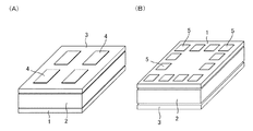
図1(A),(B)は従来の無線モジュールの構成図である。図1(B)は、図1(A)の無線モジュールを裏返した状態を示す。図1(A),(B)の無線モジュールは、第1基板1と、シールド板2と、第2基板3とを備えている。第1基板1の上面には不図示の通信回路が形成され、シールド板2によって覆われている。第2基板3の上面にはパッチアンテナ4が設けられている。第1基板1の下面には、図1(B)に示すように信号パッド5が設けられている。信号パッド5は不図示の実装基板上に半田などにより固定される。図1(A)の無線モジュールでは、アンテナ面から垂直上向きに指向性があるため、目標に対しアンテナ面を向ける必要がある。
1A and 1B are configuration diagrams of a conventional wireless module. FIG. 1B illustrates a state in which the wireless module illustrated in FIG. 1A and 1B includes a
また、上下両面にパッチアンテナを搭載した高周波通信モジュールを、開口を設けた実装基板に実装する技術が知られている(例えば、特許文献1参照)。この技術では、高周波通信モジュールの上下両面から電波を放射することができる。 In addition, a technique for mounting a high-frequency communication module in which patch antennas are mounted on both upper and lower surfaces on a mounting substrate having an opening is known (see, for example, Patent Document 1). With this technology, radio waves can be radiated from both the upper and lower surfaces of the high-frequency communication module.
また、片面が取付面で他面が装飾面の筐体にアンテナ素子を収容し、車室内のガラス面やダッシュボード上に設置される車載用アンテナ装置が知られている(例えば、特許文献2参照)。 In addition, an in-vehicle antenna device is known in which an antenna element is housed in a housing having a mounting surface on one side and a decorative surface on the other side, and is installed on a glass surface or dashboard in a vehicle interior (for example, Patent Document 2). reference).
図1(A),(B)の無線モジュールでは、第1基板1の信号パッド5を実装基板上に半田などにより固定しなければならないため、無線モジュールを実装基板上に実装する際に、実装方法及び取り付け方向は1つに限定されている。
In the wireless module shown in FIGS. 1A and 1B, the
本発明の目的は、複数の実装方法及び複数の取り付け方向を提供することができる無線モジュールを提供することにある。 An object of the present invention is to provide a wireless module capable of providing a plurality of mounting methods and a plurality of mounting directions.
上記目的を達成するため、明細書に開示された無線モジュールは、第1面と前記第1面の裏側の第2面とを有する基板と、前記第1面及び前記第2面上に設けられ、信号を入出力する複数の信号端子と、前記第1面上に設けられたアンテナと、前記第2面上に設けられ、前記複数の信号端子と前記アンテナとの間に接続され、前記複数の信号端子及び前記アンテナから入力する信号に対して各種の信号処理を行う信号処理回路とを備え、前記複数の信号端子は、前記第1面及び前記第2面上において左右対称に配置され、且つ前記第1面及び前記第2面の同じ位置に配置され、前記基板内で単一の信号線に接続されていることを特徴とする。 In order to achieve the above object, a wireless module disclosed in the specification is provided on a substrate having a first surface and a second surface on the back side of the first surface, and on the first surface and the second surface. A plurality of signal terminals for inputting and outputting signals; an antenna provided on the first surface; and a plurality of signal terminals provided on the second surface and connected between the plurality of signal terminals and the antenna. And a signal processing circuit that performs various signal processing on a signal input from the antenna, and the plurality of signal terminals are arranged symmetrically on the first surface and the second surface, And it is arrange | positioned in the same position of the said 1st surface and the said 2nd surface, and is connected to the single signal line within the said board | substrate.
本発明の無線モジュールによれば、複数の実装方法及び複数の取り付け方向を提供することができる。 According to the wireless module of the present invention, it is possible to provide a plurality of mounting methods and a plurality of mounting directions.
以下、図面を参照しながら本発明の実施の形態を説明する。 Hereinafter, embodiments of the present invention will be described with reference to the drawings.
図2(A),(B)は、本実施の形態に係る無線モジュールの外観構成図である。図2(B)は、図2(A)の無線モジュールを裏返した状態を示す。図3は、無線モジュールの側面図である。本実施の形態では、図2(A)に示すように上下左右及び前後の方向を規定する。図2(B)では上下方向及び左右方向が反転する。 2A and 2B are external configuration diagrams of the wireless module according to the present embodiment. FIG. 2B illustrates a state in which the wireless module illustrated in FIG. FIG. 3 is a side view of the wireless module. In this embodiment mode, the vertical and horizontal directions and the front and rear directions are defined as shown in FIG. In FIG. 2B, the vertical direction and the horizontal direction are reversed.
図2(A),(B)の無線モジュール10は、基板11と、コネクタ15と、シールドケース16とを備えている。基板11は上面視で十字形状であるが、基板11の形状はこれに限定されるものではない。基板11の上面20の中央には複数のパッチアンテナ12が設けられている。
The
上面20の左右両端には、信号端子として複数の信号パッド13a〜13d及び14a〜14dがそれぞれ設けられている。信号パッド13a〜13d及び14a〜14dは後述するように実装基板の信号パッド上に半田により固定される。
A plurality of
図3に示すように、信号パッド13a〜13d及び信号パッド14a〜14dは、上面20(第1面)だけではなく、基板11の下面21(第2面)にも設けられている。上面20の信号パッド13a〜13dは下面21の信号パッド13a〜13dと基板11の内部で信号線34a〜34dにより電気的に接続され、上面20の信号パッド14a〜14dは下面21の信号パッド14a〜14dと基板11の内部で信号線34a〜34dにより電気的に接続されている。なお、信号パッドの個数は、図2(A),(B)及び図3の例に限定されるものではない。
As illustrated in FIG. 3, the
基板11の下面21前端にはコネクタ15が設けられている。コネクタ15は、例えばFPC(Flexible printed circuit)用コネクタ、スタッキングコネクタ又はDIPコネクタである。
A
基板11の下面21中央には、後述する無線通信用の回路を覆い電磁波を遮断するシールドケース16が設けられている。シールドケース16は箱状である。シールドケース16の下端の4隅には、シールドケース16を冶具や製品筐体などに固定するための固定部17が設けられている。固定部17は水平に広がる薄板形状であり、半田で冶具や製品筐体などに固定するために半田の濡れ性を有している。また、固定部17は、シールドケース16を冶具や製品筐体などにねじ止めするためのねじ孔18を有する。固定部17は、半田の濡れ性及びねじ孔18の少なくとも一方を有していればよい。尚、ねじ止めのために、基板11の4隅が上面視で固定部17と重ならないように、基板11の4隅には切り欠き11Aが設けられている。
In the center of the
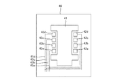
図4は、無線モジュール10の構成を示すブロック図である。
FIG. 4 is a block diagram illustrating a configuration of the
基板11の下面21中央には、変調前又は復調後の信号を扱う無線制御用のベースバンドIC31と、ベースバンドIC31からの信号を変調又は復調して無線信号を生成する無線信号生成用のRFIC32と、無線信号の送受信や増幅を行うフロントエンド回路33とが設けられている。ベースバンドIC31、RFIC32、及びフロントエンド回路33は複数の信号パッド13a〜13d,14a〜14d及びパッチアンテナ12から入力された信号に対して各種の信号処理を行う信号処理回路として機能し、シールドケース16に収納されている。
At the center of the
ベースバンドIC31は、信号線34a〜34dにより信号パッド13a〜13d、信号パッド14a〜14d及びコネクタ15に接続されており、変調前又は復調後の信号を送受信する。さらに、ベースバンドIC31は、RFIC32に接続されている。RFIC32はフロントエンド回路33に接続され、フロントエンド回路33は無線信号を電波として送受信するパッチアンテナ12に信号線35により接続されている。パッチアンテナ12は上面20に設けられ、フロントエンド回路33は下面21に設けられているので、信号線35は基板11の内部に配置されている。
The
信号パッド13a及び信号パッド14aは信号線34aに接続され、信号パッド13b及び信号パッド14bは信号線34bに接続されている。信号パッド13c及び信号パッド14cは信号線34cに接続され、信号パッド13d及び信号パッド14dは信号線34dに接続されている。また、コネクタ15は信号線34a〜34dに接続されている。尚、信号線34a〜34dは基板11の内部に設けられている。
The
図5は、無線モジュール10が実装される実装基板の構成を示す図である。
FIG. 5 is a diagram illustrating a configuration of a mounting board on which the
実装基板40は、無線モジュール10のシールドケース16を挿入可能な貫通孔41と、信号パッド13a〜13d及び信号パッド14a〜14dと半田で固定される信号パッド42a〜42d及び信号パッド43a〜43dとを備えている。信号パッド42a及び信号パッド43aは実装基板40の内部で信号線45aに接続され、信号パッド42b及び信号パッド43bは実装基板40の内部で信号線45bに接続されている。信号パッド42c及び信号パッド43cは実装基板40の内部で信号線45cに接続されており、信号パッド42d及び信号パッド43dは実装基板40の内部で信号線45dに接続されている。
The mounting
図6(A),(B)は、無線モジュール10を実装基板40に実装する状態を示す図である。図6(A)では、図2(A)の状態の無線モジュール10を実装基板40上に実装する。図6(B)では、図2(B)の裏返した状態の無線モジュール10を実装基板40上に実装する。
6A and 6B are diagrams illustrating a state in which the
図6(A)では、固定部17を含むシールドケース16及びコネクタ15が貫通孔41に挿入される。これにより、無線モジュール10と実装基板40との厚みの合計が減少し、いわゆる低背化を図ることができる。尚、図6(A)の場合、パッチアンテナ12の指向性は上向きである。
In FIG. 6A, the
また、信号パッド13a〜13dが設けられている基板11の左端及び信号パッド14a〜14dが設けられている基板11の右端は、貫通孔41に挿入されずに実装基板40の一部と接触する。信号パッド13a〜13dは実装基板40上の信号パッド43a〜43dと半田によりそれぞれ導通し、信号パッド14a〜14dは実装基板40上の信号パッド42a〜42dと半田によりそれぞれ導通する。
In addition, the left end of the
一方、図6(B)では、信号パッド13a〜13dが設けられている基板11の右端及び信号パッド14a〜14dが設けられている基板11の左端は実装基板40の一部と接触するので、固定部17を含むシールドケース16及びコネクタ15は貫通孔41に挿入されない。図6(B)の場合、パッチアンテナ12の指向性は下向きである。また、パッチアンテナ12が貫通孔41に挿入されるので、上面20からわずかに突出するパッチアンテナ12を外部から目隠しすることができる。
On the other hand, in FIG. 6B, the right end of the
図6(B)の場合、信号パッド13a〜13dは実装基板40上の信号パッド42a〜42dと半田によりそれぞれ導通し、信号パッド14a〜14dは実装基板40上の信号パッド43a〜43dと半田によりそれぞれ導通する。
In the case of FIG. 6B, the
このように、無線モジュール10において、信号パッド13a及び14a、13b及び14b、13c及び14c、又は13d及び14dを左右対称且つ上下対称に基板11上に配置し、左右対称且つ上下対称に配置された信号パッド同士を基板11内の同じ単一の信号線34a(34b〜34d)に接続することで、2つのアンテナ指向性を実現できる。尚、信号パッドの上下対称の配置とは、信号パッドが基板11の上面20及び下面21の同じ位置に配置されることを示す。また、実装基板40においても、信号パッド42a及び43a、(42b及び43b、42c及び43c、又は42d及び43d)を左右対称に配置し、左右対称に配置された信号パッド同士を実装基板40の内部で同じ単一の信号線45a(45b〜45d)に接続することで、2つのアンテナ指向性の実現を補助できる。
As described above, in the
図7(A)は、無線モジュール10を製品筐体に実装する状態を示す図である。図7(B),(C)は、無線モジュール10が実装された製品筐体の側面図である。
FIG. 7A is a diagram illustrating a state in which the
図7(A)に示すように、実装基板40以外の製品筐体50がねじ孔51を有する場合、無線モジュール10をねじ52で製品筐体50にねじ止めすることができる。この場合、ねじ52は、ねじ孔18とねじ孔51とに差し込まれ、シールドケース16が製品筐体50に固定される。尚、製品筐体50の材料はプラスチック、樹脂又は金属などのいずれが1つである。また、無線モジュール10は冶具などにねじ止めされてもよい。
As shown in FIG. 7A, when the
コネクタ15がFPCコネクタである場合、図7(B)に示すようにFPCケーブル60をコネクタ15に接続する。この場合、信号は、信号パッド13a〜13d及び信号パッド14a〜14dを使用せずに、コネクタ15を介して入出力する。パッチアンテナ12の指向性はP方向である。
When the
図7(C)に示すように、コネクタ15がスタッキングコネクタのオス又はメスである場合には、製品筐体50に設けられたスタッキングコネクタ61のメス又はオスに差し込まれる。この場合も、信号は、信号パッド13a〜13d及び信号パッド14a〜14dを使用せずに、コネクタ15を介して入出力する。パッチアンテナ12の指向性はP方向である。
As shown in FIG. 7C, when the
尚、上述したように固定部17は半田の濡れ性を有しているので、シールドケース16を製品筐体50に半田で固定してもよい。
Since the fixing
図8は、無線モジュール10の変形例の側面図である。
FIG. 8 is a side view of a modified example of the
図3では、信号パッド13a〜13d及び信号パッド14a〜14dは、基板11の上面20及び下面21に設けられているが、図8に示すように、基板11の厚みよりも大きな厚みを有する単一の信号パッド13aを基板11の上面20及び下面21から突出するように配置してもよい。つまり、上面20の信号パッド13aが基板11を貫通して、下面21の信号パッド13aと一体化されていてもよい。この場合、上面20の信号パッド13aと下面21の信号パッド13aとを接続する基板11内の信号線は不要である。
In FIG. 3, the
以上説明したように、本実施の形態によれば、複数の信号パッド13a及び14a、13b及び14b、13c及び14c、又は13d及び14dが、上面20及び下面21上において左右対称に配置され、且つ上面20及び下面21の同じ位置に配置され基板11内で単一の信号線に接続されているので、図6(A)又は図6(B)のように、パッチアンテナ12の指向性を上向き又は下向きにした状態で無線モジュール10を実装基板40に実装することができる。従って、複数の実装方法及び複数の取り付け方向を提供することができる。
As described above, according to the present embodiment, the plurality of
尚、本発明は、上述した実施の形態に限定されるものではなく、その要旨を逸脱しない範囲内で種々変形して実施することが可能である。 The present invention is not limited to the above-described embodiment, and can be implemented with various modifications within a range not departing from the gist thereof.
10 無線モジュール
11 基板
12 パッチアンテナ
13a〜13d,14a〜14d 信号パッド
15 コネクタ
16 シールドケース
34a〜34d 信号線
40 実装基板
DESCRIPTION OF
Claims (5)
前記第1面及び前記第2面上に設けられ、信号を入出力する複数の信号端子と、
前記第1面上に設けられたアンテナと、
前記第2面上に設けられ、前記複数の信号端子と前記アンテナとの間に接続され、前記複数の信号端子及び前記アンテナから入力する信号に対して各種の信号処理を行う信号処理回路とを備え、
前記複数の信号端子は、前記第1面及び前記第2面上において左右対称に配置され、且つ前記第1面及び前記第2面の同じ位置に配置され、前記基板内で単一の信号線に接続されていることを特徴とする無線モジュール。 A substrate having a first surface and a second surface behind the first surface;
A plurality of signal terminals provided on the first surface and the second surface for inputting and outputting signals;
An antenna provided on the first surface;
A signal processing circuit provided on the second surface, connected between the plurality of signal terminals and the antenna, and performing various signal processing on the signals input from the plurality of signal terminals and the antenna; Prepared,
The plurality of signal terminals are disposed symmetrically on the first surface and the second surface, and are disposed at the same position on the first surface and the second surface, and a single signal line in the substrate. A wireless module characterized by being connected to.
Priority Applications (2)
| Application Number | Priority Date | Filing Date | Title |
|---|---|---|---|
| JP2018059016A JP2019176202A (en) | 2018-03-26 | 2018-03-26 | Wireless module |
| US16/230,330 US10916827B2 (en) | 2018-03-26 | 2018-12-21 | Wireless module |
Applications Claiming Priority (1)
| Application Number | Priority Date | Filing Date | Title |
|---|---|---|---|
| JP2018059016A JP2019176202A (en) | 2018-03-26 | 2018-03-26 | Wireless module |
Publications (1)
| Publication Number | Publication Date |
|---|---|
| JP2019176202A true JP2019176202A (en) | 2019-10-10 |
Family
ID=67985662
Family Applications (1)
| Application Number | Title | Priority Date | Filing Date |
|---|---|---|---|
| JP2018059016A Pending JP2019176202A (en) | 2018-03-26 | 2018-03-26 | Wireless module |
Country Status (2)
| Country | Link |
|---|---|
| US (1) | US10916827B2 (en) |
| JP (1) | JP2019176202A (en) |
Citations (4)
| Publication number | Priority date | Publication date | Assignee | Title |
|---|---|---|---|---|
| JP2003051711A (en) * | 2001-08-07 | 2003-02-21 | Murata Mfg Co Ltd | Rf circuit integrated antenna, antenna module employing the antenna and communication equipment provided with the module |
| JP2004015160A (en) * | 2002-06-04 | 2004-01-15 | Tdk Corp | Module with antenna |
| JP2004274259A (en) * | 2003-03-06 | 2004-09-30 | Tdk Corp | Antenna integrated module and communication device |
| JP2015023360A (en) * | 2013-07-17 | 2015-02-02 | パナソニックIpマネジメント株式会社 | High frequency module |
Family Cites Families (8)
| Publication number | Priority date | Publication date | Assignee | Title |
|---|---|---|---|---|
| JP2006262164A (en) | 2005-03-17 | 2006-09-28 | Alps Electric Co Ltd | On-vehicle antenna system |
| US7830312B2 (en) * | 2008-03-11 | 2010-11-09 | Intel Corporation | Wireless antenna array system architecture and methods to achieve 3D beam coverage |
| WO2013084496A1 (en) * | 2011-12-07 | 2013-06-13 | パナソニック株式会社 | Wireless module |
| JP6299878B2 (en) | 2014-10-07 | 2018-03-28 | 株式会社村田製作所 | High frequency communication module and high frequency communication device |
| WO2017047396A1 (en) * | 2015-09-17 | 2017-03-23 | 株式会社村田製作所 | Antenna-integrated communication module and method for manufacturing same |
| WO2018173750A1 (en) * | 2017-03-21 | 2018-09-27 | 株式会社村田製作所 | Antenna module and communication device |
| US10186492B1 (en) * | 2017-07-18 | 2019-01-22 | Taiwan Semiconductor Manufacturing Co., Ltd. | Package structure and manufacturing method thereof |
| US10530038B2 (en) * | 2018-03-06 | 2020-01-07 | Advanced Semiconductor Engineering, Inc. | Semiconductor package device |
-
2018
- 2018-03-26 JP JP2018059016A patent/JP2019176202A/en active Pending
- 2018-12-21 US US16/230,330 patent/US10916827B2/en active Active
Patent Citations (4)
| Publication number | Priority date | Publication date | Assignee | Title |
|---|---|---|---|---|
| JP2003051711A (en) * | 2001-08-07 | 2003-02-21 | Murata Mfg Co Ltd | Rf circuit integrated antenna, antenna module employing the antenna and communication equipment provided with the module |
| JP2004015160A (en) * | 2002-06-04 | 2004-01-15 | Tdk Corp | Module with antenna |
| JP2004274259A (en) * | 2003-03-06 | 2004-09-30 | Tdk Corp | Antenna integrated module and communication device |
| JP2015023360A (en) * | 2013-07-17 | 2015-02-02 | パナソニックIpマネジメント株式会社 | High frequency module |
Also Published As
| Publication number | Publication date |
|---|---|
| US10916827B2 (en) | 2021-02-09 |
| US20190296417A1 (en) | 2019-09-26 |
Similar Documents
| Publication | Publication Date | Title |
|---|---|---|
| US10673142B2 (en) | Antenna module | |
| CN112438042B (en) | Antenna structure and electronic device comprising an antenna | |
| US11228120B2 (en) | Antenna and electronic device including the same | |
| US6879849B2 (en) | In-built antenna for mobile communication device | |
| KR101606145B1 (en) | Antenna device for portable terminal | |
| CN111293409A (en) | Electronic device including antenna for wireless communication | |
| KR20150025968A (en) | Device with loop type antenna | |
| JP2005091082A (en) | Antenna-integrated navigation system | |
| CN108039564A (en) | Antenna module and electronic equipment | |
| CN117378091A (en) | Antenna module and electronic device comprising same | |
| JP2019176202A (en) | Wireless module | |
| JP2003101340A (en) | Diversity antenna and radio communication device | |
| JP2013201511A (en) | Vehicle antenna integrated wireless communication module, vehicle wireless communication device, and manufacturing method for vehicle wireless communication device | |
| US20190296427A1 (en) | Antenna device | |
| JP2007329735A (en) | Wireless communication module and manufacturing method thereof | |
| EP3012904B1 (en) | Communication device and antenna thereof | |
| JP2007336279A (en) | Antenna | |
| JP2019142401A (en) | On-vehicle camera | |
| JP2006014154A (en) | Antenna | |
| KR101681902B1 (en) | Antenna structure | |
| TWI748617B (en) | Three-dimensional antenna device and carrier thereof | |
| JP7038305B2 (en) | Electronics | |
| JP2022170410A (en) | antenna device | |
| JP2022072630A (en) | Vehicle radio communication device | |
| JP2005341144A (en) | Antenna system |
Legal Events
| Date | Code | Title | Description |
|---|---|---|---|
| A621 | Written request for application examination |
Free format text: JAPANESE INTERMEDIATE CODE: A621 Effective date: 20210215 |
|
| A977 | Report on retrieval |
Free format text: JAPANESE INTERMEDIATE CODE: A971007 Effective date: 20211102 |
|
| A131 | Notification of reasons for refusal |
Free format text: JAPANESE INTERMEDIATE CODE: A131 Effective date: 20211207 |
|
| A02 | Decision of refusal |
Free format text: JAPANESE INTERMEDIATE CODE: A02 Effective date: 20220531 |